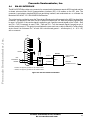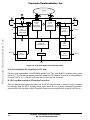
1
MOTOROLA
Freescale Semiconductor, Inc.
SEMICONDUCTOR TECHNICAL DATA
Order this document
by MC145572EVK/D
Advance Information
MC145572EVK
Freescale Semiconductor, Inc...
ISDN U-Interface Transceiver Evaluation Kit
This document contains information on a new product. SpeciÞcations and information herein are subject to change without notice.
REV 2
11/97
For More Information On This Product,
Go to: www.freescale.com
Freescale Semiconductor, Inc.
CONTENTS
Paragraph
Number
Page
Number
Title
Freescale Semiconductor, Inc...
SECTION 1
INTRODUCTION
5
1.1
ORGANIZATION OF DATA SHEET . . . . . . . . . . . . . . . . . . . . . . . . . . . . . . . . . .
5
1.2
INTRODUCTION . . . . . . . . . . . . . . . . . . . . . . . . . . . . . . . . . . . . . . . . . . . . . . . . .
5
1.3
FEATURES . . . . . . . . . . . . . . . . . . . . . . . . . . . . . . . . . . . . . . . . . . . . . . . . . . . . .
1.3.1 General. . . . . . . . . . . . . . . . . . . . . . . . . . . . . . . . . . . . . . . . . . . . . . . . . . .
1.3.2 Hardware . . . . . . . . . . . . . . . . . . . . . . . . . . . . . . . . . . . . . . . . . . . . . . . . .
1.3.3 Software . . . . . . . . . . . . . . . . . . . . . . . . . . . . . . . . . . . . . . . . . . . . . . . . . .
7
7
7
7
1.4
BLOCK DIAGRAM . . . . . . . . . . . . . . . . . . . . . . . . . . . . . . . . . . . . . . . . . . . . . . . .
8
1.5
GETTING STARTED . . . . . . . . . . . . . . . . . . . . . . . . . . . . . . . . . . . . . . . . . . . . . .
8
SECTION 2
HARDWARE REFERENCE
12
2.1
U-INTERFACE . . . . . . . . . . . . . . . . . . . . . . . . . . . . . . . . . . . . . . . . . . . . . . . . . . .
2.1.1 Line Interface Circuitry . . . . . . . . . . . . . . . . . . . . . . . . . . . . . . . . . . . . . . .
2.1.2 Crystal Oscillator (LT Mode). . . . . . . . . . . . . . . . . . . . . . . . . . . . . . . . . . .
2.1.3 Crystal Oscillator (NT Mode) . . . . . . . . . . . . . . . . . . . . . . . . . . . . . . . . . .
12
12
14
14
2.2
S/T-INTERFACE . . . . . . . . . . . . . . . . . . . . . . . . . . . . . . . . . . . . . . . . . . . . . . . . .
14
2.3
MICROCONTROLLERS . . . . . . . . . . . . . . . . . . . . . . . . . . . . . . . . . . . . . . . . . . .
2.3.1 Status LEDs . . . . . . . . . . . . . . . . . . . . . . . . . . . . . . . . . . . . . . . . . . . . . . .
15
15
2.4
EIA-232 INTERFACE. . . . . . . . . . . . . . . . . . . . . . . . . . . . . . . . . . . . . . . . . . . . . .
16
2.5
BIT ERROR ANALYZER INTERFACE . . . . . . . . . . . . . . . . . . . . . . . . . . . . . . . .
2.5.1 Setting Up a Bit Error Rate Test. . . . . . . . . . . . . . . . . . . . . . . . . . . . . . . .
17
19
2.6
MC145572EVK TEST HEADERS . . . . . . . . . . . . . . . . . . . . . . . . . . . . . . . . . . . .
2.6.1 NT Signal Header (JP7) Pin Descriptions . . . . . . . . . . . . . . . . . . . . . . . .
2.6.2 LT Signal Header (JP26) Pin Descriptions. . . . . . . . . . . . . . . . . . . . . . . .
22
24
27
2.7
DIP SWITCH FUNCTIONS . . . . . . . . . . . . . . . . . . . . . . . . . . . . . . . . . . . . . . . . .
2.7.1 NT Side GCI Parameters DIP Switch S1 . . . . . . . . . . . . . . . . . . . . . . . . .
2.7.2 NT Side Configuration DIP Switch S4 . . . . . . . . . . . . . . . . . . . . . . . . . . .
2.7.3 LT Side GCI Parameters DIP Switch S1 . . . . . . . . . . . . . . . . . . . . . . . . .
2.7.4 LT Side Configuration DIP Switch S7. . . . . . . . . . . . . . . . . . . . . . . . . . . .
30
30
31
31
32
2.8
POWER SUPPLY . . . . . . . . . . . . . . . . . . . . . . . . . . . . . . . . . . . . . . . . . . . . . . . .
32
SECTION 3
SOFTWARE DESIGN DESCRIPTION
3.1
33
OPERATING PROCEDURES . . . . . . . . . . . . . . . . . . . . . . . . . . . . . . . . . . . . . . .
3.1.1 Power On Reset and Terminal Prompt . . . . . . . . . . . . . . . . . . . . . . . . . .
3.1.2 Command Line Interface . . . . . . . . . . . . . . . . . . . . . . . . . . . . . . . . . . . . .
3.1.3 Push-Button Activation . . . . . . . . . . . . . . . . . . . . . . . . . . . . . . . . . . . . . . .
3.1.4 General Comments About Activation . . . . . . . . . . . . . . . . . . . . . . . . . . . .
3.1.5 Embedded Operations Channel, Register R6 . . . . . . . . . . . . . . . . . . . . .
For More Information On This Product,
Go to: www.freescale.com
33
33
33
34
34
34
MC145572EVK
3
Freescale Semiconductor, Inc.
CONTENTS (Continued)
Paragraph
Number
Freescale Semiconductor, Inc...
3.2
Title
Page
Number
COMMAND SET . . . . . . . . . . . . . . . . . . . . . . . . . . . . . . . . . . . . . . . . . . . . . . . . .
3.2.1 ACT Ñ Activation/Deactivation Menu . . . . . . . . . . . . . . . . . . . . . . . . . . .
3.2.2 BRL Ñ Read/Write LT U-Interface Transceiver Byte Register . . . . . . . .
3.2.3 BRN Ñ Read/Write NT U-Interface Transceiver Byte Register . . . . . . . .
3.2.4 BRS Ñ Read/Write S/T-Interface Transceiver Register . . . . . . . . . . . . .
3.2.5 BRT Ñ Read/Write S/T-Interface Transceiver Byte Register . . . . . . . . .
3.2.6 CLR Ñ Clear febe/nebe Registers. . . . . . . . . . . . . . . . . . . . . . . . . . . . . .
3.2.7 DEA Ñ Activation/Deactivation Menu . . . . . . . . . . . . . . . . . . . . . . . . . . .
3.2.8 DIS Ñ Display Formatted Registers . . . . . . . . . . . . . . . . . . . . . . . . . . . .
3.2.9 eoc Ñ Embedded Operations Channel Menu . . . . . . . . . . . . . . . . . . . . .
3.2.10 HEL Ñ Help Menu . . . . . . . . . . . . . . . . . . . . . . . . . . . . . . . . . . . . . . . . . .
3.2.11 LOF Ñ Disable LT M4 Handler . . . . . . . . . . . . . . . . . . . . . . . . . . . . . . . .
3.2.12 LON Ñ Enable LT M4 Handler . . . . . . . . . . . . . . . . . . . . . . . . . . . . . . . .
3.2.13 LPU Ñ U-Interface Transceiver Analog Loop-Backs . . . . . . . . . . . . . . . .
3.2.14 MM Ñ Modify Memory . . . . . . . . . . . . . . . . . . . . . . . . . . . . . . . . . . . . . . .
3.2.15 NOF Ñ Disable NT1 Function . . . . . . . . . . . . . . . . . . . . . . . . . . . . . . . . .
3.2.16 NON Ñ Enable NT1 Function . . . . . . . . . . . . . . . . . . . . . . . . . . . . . . . . .
3.2.17 NRL Ñ Read/Write LT U-Interface Transceiver Nibble Register . . . . . . .
3.2.18 NRN Ñ Read/Write NT U-Interface Transceiver Nibble Register . . . . . .
3.2.19 NRS Ñ Read/Write S/T-Interface Transceiver Nibble Register . . . . . . . .
3.2.20 NRT Ñ Read/Write S/T-Interface Transceiver Nibble Register . . . . . . . .
3.2.21 ORL Ñ Read/Write LT U-Interface Transceiver Byte Register . . . . . . . .
3.2.22 ORN Ñ Read/Write NT U-Interface Transceiver Overlay Register . . . . .
3.2.23 RES Ñ Reset S/T-Interface Transceiver and/or U-Interface Transceivers
34
35
37
38
38
39
39
39
39
41
43
44
44
44
46
47
47
47
48
49
49
50
50
51
MC145572EVK
4
For More Information On This Product,
Go to: www.freescale.com
Freescale Semiconductor, Inc.
LIST OF FIGURES
Freescale Semiconductor, Inc...
Paragraph
Number
Figure 1-1.
Figure 1-2.
Figure 1-3.
Figure 1-4.
Figure 2-1.
Figure 2-2.
Figure 2-3.
Figure 2-4.
Figure 2-5.
Figure 2-6.
Figure 2-7.
Figure 2-8.
Figure 2-9.
Title
Page
Number
Motorola Silicon Applications and the MC145572EVK . . . . . . . . . . . . . . . . .
MC145572EVK Functional Block Diagram . . . . . . . . . . . . . . . . . . . . . . . . . .
MC145572EVK DIP Switch Configuration . . . . . . . . . . . . . . . . . . . . . . . . . . .
External Connections to the MC145572EVK . . . . . . . . . . . . . . . . . . . . . . . . .
NT Line Interface Schematic and Component Values . . . . . . . . . . . . . . . . . .
LT Line Interface Schematic and Component Values . . . . . . . . . . . . . . . . . .
EIA-232 Interface Schematic . . . . . . . . . . . . . . . . . . . . . . . . . . . . . . . . . . . . .
Access to Bit Error Analyzer Interface Through J22 and J9 Headers . . . . . .
BERT Gated Clock Ñ 8-Bit Gated Clock . . . . . . . . . . . . . . . . . . . . . . . . . . . .
BERT Gated Clock Ñ 10-Bit Gated Clock . . . . . . . . . . . . . . . . . . . . . . . . . . .
Bit Error Rate Test Set-Up NT Side . . . . . . . . . . . . . . . . . . . . . . . . . . . . . . . .
Loop-Back Modes for the MC145572EVK . . . . . . . . . . . . . . . . . . . . . . . . . . .
Power Connector Pin Assignments . . . . . . . . . . . . . . . . . . . . . . . . . . . . . . . .
7
9
10
11
14
14
17
18
19
19
21
22
33
For More Information On This Product,
Go to: www.freescale.com
MC145572EVK
5
Freescale Semiconductor, Inc.
1
Freescale Semiconductor, Inc...
INTRODUCTION
1.1
ORGANIZATION OF DATA SHEET
This document is composed of three major sections. Section 1 introduces the MC145572EVK U-Interface
Transceiver Evaluation Kit with a brief description of the evaluation board and a list of key features. Also
included at the end of Section 1 is ÒGetting Started,Ó a short tutorial to help begin working with the
MC145572EVK. Section 2 is a brief description of the hardware design. Section 3 contains the command
set descriptions and examples.
IMPORTANT NOTE
This UserÕs Manual Ñ MC145572EVK U-Interface Transceiver Evaluation Kit Revision 2
Ñ corresponds with MC145572EVK Printed Circuit Board Revision F with Þrmware version
2.01. If a discrepancy exists between this document and the MC145572 data sheet, the
MC145572 data sheet should take precedence.
1.2
INTRODUCTION
The MC145572EVK U-Interface Transceiver Evaluation Kit provides Motorola ISDN customers a
convenient and efÞcient vehicle for evaluation of the MC145572 ISDN U-Interface Transceiver. The
approach taken to demonstrate the MC145572 U-Interface Transceiver is to provide the user with a fully
functional NT1 (Network Termination Type 1) connected to an LT (Line Termination). An NT1 provides
transparent 2B+D data transfer between the U- and S/T-Interfaces. In addition, it provides for network
initiated maintenance procedures. The MC145572EVK does not terminate any ISDN call control
messages. It also does not terminate any maintenance messages received over the S/T-Interface.
The MC145572EVK U-Interface Transceiver Evaluation Kit can be used as an NT1 card or as an LT card.
The left half of the card is the NT1, while the right half of the card is the LT. Alternatively, it can be thought
of as having both ends of the two-wire U-Interface, extending from the customer premise (NT1) to the
switch line card (LT) on a single, stand-alone evaluation board. Figure 1-1 shows a typical ISDN application
using the MC145572 and the MC145574.
The kit provides the ability to interactively manipulate status registers in the MC145572 U-Interface
Transceiver as well as in the MC145574 S/T-Interface Transceiver with the aid of an external terminal. A
unique combination of hardware and software features allows for stand-alone or terminal activation of the
U-Interface and as such provide an excellent platform for NT1 and LT hardware/software development.
The NT1 function can be disabled by putting DIP switch S4-10 in the NT1 DIS position.
MC145572EVK
6
For More Information On This Product,
Go to: www.freescale.com
SCP
For More Information On This Product,
Go to: www.freescale.com
MC145480
CODEC
X-FRMRS AND LINE I/F
IDL BUS
TA
MC145480
CODEC
X-FRMRS AND LINE I/F
IDL BUS
HOST BUS
MCMC68SC302
CLOCK SCP
MC145574
S/T-INTERFACE
MC145574
S/T-INTERFACE
CLOCK
MCMC68SC302
HOST BUS
TA
MC145480
CODEC
IDL BUS
HOST BUS
MCMC68SC302
CLOCK SCP
MC145572
U-INTERFACE
X-FRMRS AND LINE I/F
NT1/TE1
MC145574
S/T-INTERFACE
X-FRMRS AND LINE I/F
NT1
MCU
SCP
IDL
Freescale Semiconductor, Inc...
MC145572
U-INTERFACE
MC145572
U-INTERFACE
SWITCHING
EQUIPMENT
LT
MC145572
U-INTERFACE
LT
Freescale Semiconductor, Inc.
Figure 1-1. Motorola Silicon Applications and the MC145572EVK
MC145572EVK
7
Freescale Semiconductor, Inc.
1.3
FEATURES
1.3.1
·
·
·
·
Provides Stand-Alone NT1 and LT on Single Board
On-Board 68HC05 Microcontroller with Resident Monitor Software
Convenient Access to Key Signals
NT1 and LT Software Development Platform
Freescale Semiconductor, Inc...
1.3.2
·
·
·
·
·
·
·
Hardware
+ 5 V Only Power Supply
ÒPush-ButtonÓ Activation of U-Interface from NT1
Stand-Alone Operation for Bit Error Rate Testing
Gated Data Clocks Provided for Bit Error Rate Testing
Can Be Used as a U- or S/T-Interface Terminal Development Tool
On-Board 5 ppm LT Frequency Reference
EIA-232 (V.28) Serial Port for Terminal Interface
1.3.3
·
·
·
·
·
·
·
General
Software
Stand-Alone or Terminal Operation
Resident Firmware Monitor for User Control of Board
Activation and Deactivation Menus
Embedded Operations Channel
Microcontroller Controlled or Automatic Activation/Deactivation
Access to All Maintenance Channels
MC68HC05 Assembly Language Source Code Available
MC145572EVK
8
For More Information On This Product,
Go to: www.freescale.com
Freescale Semiconductor, Inc.
1.4
BLOCK DIAGRAM
Following is a basic functional block diagram for the MC145572EVK U-Interface Transceiver Evaluation
Kit (Figure 1-2). While the board is capable of activating Òstand-alone,Ó the user may decide to use a single
ASCII terminal to gain total control of the MC145572EVKÕs activities.
NT U-INTERFACE
LT U-INTERFACE
NETWORK TERMINATION
MC145572
ISDN
U-INTERFACE
TRANSCEIVER
IDL
Freescale Semiconductor, Inc...
S/T
MC145574
ISDN
S/T-INTERFACE
TRANSCEIVER
MC145572
ISDN
U-INTERFACE
TRANSCEIVER
LINE TERMINATION
IDL
REFERENCE
CLOCK
GENERATOR
EXT CLK
SCP
BERTCLK
GATED
CLOCK
GENERATOR
MC68HC705
MICROCONTROLLER
5 ppm
CLOCK
SOURCE
MC145407
GATED
CLOCK
GENERATOR
BERTCLK
RS-232
Figure 1-2. MC145572EVK Functional Block Diagram
1.5
GETTING STARTED
This section is provided to facilitate the userÕs introduction to the MC145572EVK. To maximize efÞciency
when working with the MC145572EVK, it is recommended that the user become familiar with the
organization of this document as well as the MC145572 U-Interface Transceiver data sheet. To identify a
starting point, power up the board and activate the U-Interface immediately. The only equipment needed
is a 5 V, 250 mA power supply, a two-wire U-Interface cable, and the MC145572EVK.
NOTE
The board shipped from the factory was thoroughly tested and veriÞed to function properly
prior to shipment. If you experience any problems or difÞculties with the operation of the
MC145572EVK, do not hesitate to call the factory or your local Motorola representative for
assistance.
1. Remove the board from its conductive environment at a static-controlled station.
2. Examine the board and its components to make certain nothing was damaged during shipment of
the board.
3. Verify that the ICs are seated properly in the socket.
For More Information On This Product,
Go to: www.freescale.com
MC145572EVK
9
Freescale Semiconductor, Inc.
4. Become familiar with the layout and the various connectors. Locate the power connector J19.
Locate the U-Interface connectors, J2 (LT U-Interface side) and J12 (NT U-Interface side).
The DIP switches arrive preset from the factory (see Figure 1-3). Refer also to DIP Switch Functions in
Section 2.8, for an explanation of the function of each switch. Do not change the position of any DIP switch
until you are completely familiar with its function.
NT U CONFIG
Freescale Semiconductor, Inc...
OPEN
LT U CONFIG
S4
S2
CLOSED
CLOSED
OPEN
FRON
1
RFOFF
MAS
1
SLV
FSR
2
FSX=FSR
MAS
2
SLV
8
3
10
FSR
3
FSX=FSR
IDL2
4
GCI
8
4
10
PAR
5
SER
IDL2
5
GCI
T_MAS
6
T_SLV
PAR
6
SER
7
RESMCU
7
RF=FSR
FIX
8
ADP
8
TE
9
NT
NT1EN
10
NT1DIS
NT GCI CONFIG
OPEN
S3
LT GCI CONFIG
CLOSED
OPEN
CLOSED
S1
S0HI
1
S0LOW
SOHI
1
S0LOW
S1HI
2
S1LOW
S1HI
2
S1LOW
S2HI
3
S2LOW
S2HI
3
S2LOW
GCI2048
4
GCI512
GCI2048
4
GCI512
IN1HI
5
IN1LOW
IN1HI
5
IN1LOW
IN2HI
6
IN2LOW
IN2HI
6
IN2LOW
Figure 1-3. MC145572EVK DIP Switch Configuration
MC145572EVK
10
For More Information On This Product,
Go to: www.freescale.com
Freescale Semiconductor, Inc.
ISDN LOOP
SIMULATOR
5 V/250 mA
+5
GND
EIA-232C
Freescale Semiconductor, Inc...
J12
J2
PB1
J19
J16
TERMINAL
LT
NT
PB2
Figure 1-4. External Connections to the MC145572EVK
The board is now ready for power.
5. Connect + 5 V and ground leads to the proper pins on J19.
Make certain the integrity of the power supply being used has been veriÞed to prevent any damage to the
MC145572EVK.
6. Turn the power supply on.
If everything is okay, the red LED ÒD27Ó near the power connector will be illuminated.
7. Connect a twisted pair between the two RJ-45 connectors, J12 and J2, at the top of the board.
This is the ÒU-loop.Ó
8. Depress the RESET push-button (PB1). This push-button is located adjacent to the power
connector.
9. Now depress the push-button marked ACT/DEA (PB2) located near the status LEDs.
The yellow TP/AIP status LEDs on both the NT1 and LT sides should illuminate, followed by both green
LEDs, SFS and LINKUP. This activation process should occur within 15 seconds. The NT side default
activation mode is an NT1 so the S/T-Interface is also trying to activate by continually transmitting the
INFO1 state on the S/T-Interface. If the red LED EI comes on, indicating an activation error has occurred,
re-check the integrity of the connections (i.e., does the ÒU-loopÓ twisted pair show continuity?). Retry if
necessary.
For More Information On This Product,
Go to: www.freescale.com
MC145572EVK
11
Freescale Semiconductor, Inc.
10. If available, connect an ASCII terminal to J16 (the DB-25 connector on the NT1 side of the board).
Make certain the terminal is set for 9600 baud, 1 stop bit, and no parity. If there is no response,
reverse the EIA-232 Tx and Rx signals by changing the jumpers on JP13.
11. Depress the RESET push-buttons and verify that the ÒNTLT>Ó prompt has appeared on the terminal
screen.
Freescale Semiconductor, Inc...
Continue reading this document to learn more about the operation of the MC145572EVK U-Interface
Transceiver Evaluation Kit. As always, please phone the factory for assistance with any problems
encountered while ÒGetting Started.Ó
MC145572EVK
12
For More Information On This Product,
Go to: www.freescale.com
Freescale Semiconductor, Inc.
2
Freescale Semiconductor, Inc...
HARDWARE REFERENCE
NOTE
Refer to the MC145572EVK Printed Circuit Board and to the MC145572 U-Interface
Transceiver data sheet to supplement this section. Please contact the factory before
committing design to PCB to be guaranteed notiÞcation of any improvements to the following
circuitry. The schematic of the MC145572EVK is in Appendix A of this manual.
2.1
U-INTERFACE
The U-Interface is implemented with MotorolaÕs single chip MC145572 U-Interface Transceiver (U10 on
the NT1 and U1 on the LT side), providing ISDN Basic Rate Access capability for twisted-pair loops with
conformance to ANSI T1.601-1992. For additional speciÞcations on designing with and the operation of
the MC145572, refer to the MC145572 U-Interface Transceiver data sheet in addition to this document.
2.1.1
Line Interface Circuitry
While the published speciÞcations for the U-Interface Transformer are intended as such, it is realized that
application speciÞc parameters (i.e., primary protection) may cause some variation in transformer
speciÞcations or published line interface values. Figure 2-1 (representing the NT) and Figure 2-2
(representing the LT) show the suggested architecture of the line interface. The schematic gives the
corresponding values used to interface the MC145572 to the line using Pulse Engineering PE68628
transformer. Currently all resistor values are accurate to 1%.
Secondary protection on the MC145572EVK for the NT1 side and the LT side are implemented using a
simple diode bridge consisting of four MMBD7000LT1s (D5, D6 on LT side and D18, D19 on NT1 side) to
clamp voltage surges to the power supply rail and to ground. Two populated two surge suppressors (D14,
D15, D22 on the NT1 side and D1, D2, D7 on the LT side) are on the line side of the transformer. The
circuit board has been laid out to allow resistors to be included in the line side circuitry to provide voltage
spike and power cross protection. These resistors, R17, R21 on the NT side and R1, R6 on the LT side,
are populated and jumpers are installed at JP8, JP11 on the NT1 side and JP3, JP20 on the LT side. The
jumpers can be inserted if it is desired to bypass the line side protection circuitry. The MC145572EVK
does not directly address the issue of primary protection.
For More Information On This Product,
Go to: www.freescale.com
MC145572EVK
13
Freescale Semiconductor, Inc.
JP8
+5 V
J14
1
R17
2
D18
R19
JP7
TxP
D15
R18
1
RxP
2
C33
C37
MC145572
3
2
D14
1
4
RJ45
5
R20
JP9
RxN
6
Freescale Semiconductor, Inc...
D19
7
D22
8
R22
J12
TxN
+5V
R21
1 : 1.25
R23
1
JP11
2
T2
J13
JP12
Figure 2-1. NT Line Interface Schematic and Component Values
JP3
+5V
JP4
1
R1
2
D5
R3
JP2
TxP
D2
1
R2
RxP
2
C37
C8
MC145572
3
2
D1
1
4
RJ45
5
R5
JP4
RxN
6
D6
7
D7
8
R7
TxN
J12
+5V
R6
1 : 1.25
R8
1
JP5
2
T1
J3
Figure 2-2. LT Line Interface Schematic and Component Values
MC145572EVK
14
For More Information On This Product,
Go to: www.freescale.com
JP6
Freescale Semiconductor, Inc.
2.1.2
Crystal Oscillator (LT Mode)
In the LT mode, the internal phase locked loop (PLL) of the MC145572 generates a 20.48 MHz clock which
is phase locked to an 8 kHz reference clock applied at the FREQREF pin. This assures that the transmitted
2B1Q signal is synchronized to the 8 kHz frequency reference. A single pullable crystal, Y1, is all that is
required for the MC145572 oscillator. All other frequency pulling circuitry is internal to the MC145572.
It is also possible to provide an external 8 kHz frequency reference rather than using the 8 kHz frequency
reference generated on-board from the 5 ppm oscillator, Y5. This is accomplished using the RFoff-RFon
switch of S2-1 and connecting the external reference to EXTREF of J9. RFoff selects the off-board 8 kHz
frequency reference and RFon selects the on-board 8 kHz frequency reference. See also the explanation
for S2-1 and S2-7 in Section 2.7.2.
Freescale Semiconductor, Inc...
2.1.3
Crystal Oscillator (NT Mode)
The NT-conÞgured MC145572 U10, requires only a single pullable crystal, Y2, for its oscillator. All other
frequency pulling circuitry is internal to the MC145572.
2.2
S/T-INTERFACE
The S/T-Interface resides on the NT1 portion of the MC145572EVK and is implemented using the
MC145574 S/T-Interface Transceiver (U17). The 600 mil 28-pin Plastic SOIC MC145574 conforms to both
CCITT I.430 and ANSI T1.605 speciÞcations. External line interface circuitry for switching between NT
and TE operating modes is incorporated.
Two 8-pin RJ-45 telephone jacks are used at the S/T-Interface, one conÞgured for the NT mode (J24) of
operation and one conÞgured for the TE mode (J23) of operation. The Tx pair, pins 4 and 5 on the NT jack
and pins 3 and 6 on the TE jack, are driven by the TxP and TxN pins which act as a current limited differential
voltage source. The drive resistance (R40, R42) is necessary to conform to the ANSI T1.605 pulse mask
speciÞcation. A dual 2.5:1 turns ratio transformer (T4A:B) is used to couple the Tx and Rx pairs to the
4-wire interface. A high frequency 4-wire common mode choke transformer (T3 for TE and T5 for NT)
provides an effective means of compliance with EMI suppression.
The protection diodes (D29A:G, D30A:G MMAD1108) provide secondary protection to the MC145574,
even when it is powered down, without loading the S/T-Interface bus. CCITT I.430, ETSI ETS 300012, and
ANSI T1.605 specify that the S/T-interface voltage cannot exceed 1.6 times the nominal voltage of 750 mV
(= 1.2 V). Since the MC145574 is designed to operate with 2.5:1 turns ratio transformers, the diode structure
is required to provide protection, while not adversely affecting the S/T-interface when power is removed
from the device. This diode structure also protects the circuit against electrostatic discharges (ESD) and
latch-up.
The S/T-Interface Transceiver implementation on this board can be used in either NT or TE mode. Pin 4,
TE/NT(L), of the MC145574 determines whether the chip is in NT or TE mode of operation. When
conÞgured as a TE, pins 9 and 8 are used as DREQUEST and DGRANT, respectively. The DREQUEST
pin is used by an external controller such as the MC145488 DDLC or the MC68302 IMP to request access
to the D-Channel. When the S/T-Interface Transceiver gains access to the D-Channel time slot on the
S/T-Interface bus, it asserts DGRANT high, informing the external controller that it can transmit its
D-Channel data in the next IDL D time slot. In the NT mode, pin 6 performs the FIX and TFSC functions.
FIX tells the S/T-Interface Transceiver to use Fixed or Adaptive timing recovery. TFSC is asserted when
frame synchronization has been achieved at the S/T-Interface bus. For a more complete discussion on
D-Channel operation, please refer to Section 11 of the MC145574/75 S/T-Interface Transceiver data
manual.
With the left side of the board operating as an NT1, the MC145574 S/T-Interface Transceiver is in the NT
mode, operating as an IDL Slave, and is receiving its Clock and Sync signals from the MC145572
For More Information On This Product,
Go to: www.freescale.com
MC145572EVK
15
Freescale Semiconductor, Inc.
U-Interface Transceiver. Access to the control registers within the S/T-Interface Transceiver is gained
through the SCP Interface. The registers are displayed and changed via resident software on the
MC145572EVK. A complete description of the S/T-Interface Transceiver registers can be found in Sections
8, 9, and 10 of the MC145574 S/T-Interface Transceiver data sheet.
2.3
MICROCONTROLLERS
Freescale Semiconductor, Inc...
The MC145572EVK is an MC68HC705C8 microcontroller-based system. One microcontroller resides on
the board; U15 on the NT1 side which controls both the NT1 and the LT sides. The hardware RESET
push-button is located next to the power supply connection for the microcontroller. U5 must be populated
for the display LEDs to operate properly.
The U-Interface may be activated using an ASCII terminal connected to the EIA-232 (V.28) port marked
J16 on the NT1 side. The board may be activated as it Òstands aloneÓ with the push of a button. The default
activation mode for the Activate/Deactivate push-button, PB2 (located near the front of the board), is as
an NT1, with INFO1 continually transmitted on the S/T-Interface until it receives INFO2. When DIP switch
S4-10 is in the NT1DIS position, the NT1 functionality is disabled. The LT side initiates activation on the
U-Interface. Eight status LEDs (D10, D11, D12, and D13 on LT side and D23, D24, D25, and D26 on the
NT1 side) are continuously updated by the MC68HC705C8s to provide the user with a visual update of
the U-Interface activation status.
When the MC145572EVK is reset, it defaults to NT1 function enabled and automatic handling of M4
maintenance channel on the LT side U-transceiver. The NT1 function can also be disabled by entering the
ÒNOFÓ command. The LT maintenance can be disabled by entering the ÒLOFÓ command. See Section 3.2
for more information on LOF, LON, NOF, and NON commands.
2.3.1
Status LEDs
Ten status LEDs are provided on the MC145572EVK to offer the user a quick visual update to critical
status parameters.
One red LED, D27 on the LT, is located near the power connector and is illuminated when + 5 V is applied
to the board.
One green LED (D31) marked S/T ACT located near the PB2 (ACT/DEA) push button, illuminates to
indicate that the MC145574 when conÞgured as an NT has achieved frame synchronization.
Located on both sides of the board are four LEDs representing Nibble Register 1 (NR1) of each U-Interface
Transceiver. The LEDs in each bank are each marked with LINKUP, EI, SFS, and TP/AIP. They map directly
to the register contents as shown below.
b3
b2
b1
b0
NR1
Linkup
Error Indication
Superframe Sync
Transparent/
Activation in Progress
NT (LED
Silkscreen)
NT LINKUP
NT EI
NT SFS
NT TP/AIP
LT (LED
Silkscreen)
LT LINKUP
LT EI
LT SFS
LT TP/AIP
NOTE
The received data is not transmitted on the IDL2 Interface until Linkup is a 1, SFS is a 1,
TP/AIP is a 1, and either CustEn (see NR2 in MC145572 U-Interface Transceiver data
sheet) or VerifAct is a 1 (see BR9 in MC145572 U-Interface Transceiver data sheet).
MC145572EVK
16
For More Information On This Product,
Go to: www.freescale.com
Freescale Semiconductor, Inc.
2.4
EIA-232 INTERFACE
The MC145572EVK provides one connector for communication between a remote ASCII terminal and the
on-board microcontroller Serial Communications Interface (SCI). J16 resides on the NT1 side. The
connector is an industry standard DB-25 type and bring, transmit, and receive data on- or off-board via
MotorolaÕs MC145407 + 5 V EIA-232D Driver/Receiver.
J16
24
23
22
21
20
GROUND
19
18
17
DATA
TO/FROMASCII
TERMINAL
16
15
14
13
1*
12
2**
11
10
9
8
7
6
5
Tx3Rx2
25
Rx3Tx2
Freescale Semiconductor, Inc...
The option is also provided to swap the Transmit and Receive pins with respect to the ASCII terminal data
connector. This appears in the form of a set of jumpers located near J16. With the jumpers populated as
in case 1 in Figure 2-3, the receive signal is present on pin 2 and the transmit signal on pin 3 (Rx2 Ð Rx2
and Tx3 Ð Tx3). Conversely in case 2, Rx2 Ð Rx2 and Tx3 Ð Tx3, the transmit signal is present on pin 2
and the receive on pin 3. This option is useful when the user must use a cable in which the Tx/Rx polarity
at pins 2 and 3 is not known. Pin 7 of both J16 is circuit board ground Ñ all other pins (1, 4 Ð 6, 8 Ð 25)
are no connects.
MC145407
Rx INPUT
4
Rx2
3
DO3Tx3
2
Tx OUTPUT
DI3
1
TO MCU RECEIVE
DATA IN
FROM MCU
TRANSMIT DATA OUT
* Rx3Tx2, with jumpers populated on this vertical column.
** Tx3Rx2, with jumpers populated on this vertical column.
Figure 2-3. EIA-232 Interface Schematic
For More Information On This Product,
Go to: www.freescale.com
MC145572EVK
17
Freescale Semiconductor, Inc.
2.5
BIT ERROR ANALYZER INTERFACE
The MC145572EVK ISDN U-Interface Evaluation Kit provides TTL-compatible gated clocks for the B1,
B2, and D time slots to allow easy connection to a bit error rate tester. This is accomplished with the use
of glue logic. Access to these gated clock signals is through the 2 x 20 headers (J9 on the LT side and
J22 on the NT1 side). Figure 2-4 details the connections on both of these headers. The clocks are output
in either an 8- or 10-bit boundary mode at the IDL clock speed.
The MC145572EVK is shipped from the factory conÞgured so its gated clock outputs are derived from the
TSEN output, pin 25, gated with the DCL signal from the IDL2 interface. The 2B+D format is the IDL 10-bit
frame. It can be changed to IDL 8-bit frame format by setting BR7(b0) to a 1 in the appropriate U Transceiver.
Freescale Semiconductor, Inc...
1
2
1
2
DREQ
GND
LTFREF
GND
DGRANT
GND
EXTREF
GND
NTSCPENL
GND
GND
STSCPENL
GND
GND
LTSCPENL
GND
LTSCPENL
GND
SCPCLK
GND
SCPCLK
GND
SCPTX
GND
SCPTX
GND
SCPRX
GND
SCPRX
GND
NTIRQL
GND
LTIRQL
GND
NTIDLCLK
GND
LTIDLCLK
GND
NTIDLRX
GND
LTIDLRX
GND
NTIDLTX
GND
LTIDLTX
GND
NTFSR
GND
LTFSR
GND
NTFSX
GND
LTFSX
GND
IRQLT
GND
8 kHz
GND
NTSFAR
GND
LTSFAR
GND
NTSFAX
GND
LTSFAX
GND
NTFREF
GND
NTFREFO
GND
LTFREFO
GND
NTGTCLK
GND
LTGTCLK
GND
39
GND
40
J22 (NT)
39
40
J9 (LT)
Figure 2-4. Access to Bit Error Analyzer Interface Through J22 and J9 Headers
MC145572EVK
18
For More Information On This Product,
Go to: www.freescale.com
Freescale Semiconductor, Inc.
The timing diagrams for each of these modes are shown in Figure 2-5 and Figure 2-6. One example of a
bit error rate test set-up is explained in the following section.
DCL
FSR
B1
B1
B1
B1
B1
B1
B1
B1
B2
B2
B2
B2
B2
B2
B2
B2
D
D
B1
B1
B1
B1
B1
B1
B1
B1
B2
B2
B2
B2
B2
B2
B2
B2
D
D
DOUT
Freescale Semiconductor, Inc...
DIN
(TSEN)
"
LTSFAR
NTSFAR
LTGTCLK
NTGTCLK
NOTE: These clocks are available only when either OR7(b5) or OR8(b3) is set to 1. The example shown is for when the MC145572
is conÞgured as follows: BR7(b0)=1, OR7(b5)=1, OR8(b3)=1.
Figure 2-5. BERT Gated Clock Ñ 8-Bit Gated Clock
DCL
FSR
B1
B1
B1
B1
B1
B1
B1
B1
D
B2
B2
B2
B2
B2
B2
B2
B2
D
B1
B1
B1
B1
B1
B1
B1
B1
D
B2
B2
B2
B2
B2
B2
B2
B2
D
DOUT
DIN
(TSEN)
"
LTSFAR
NTSFAR
LTGTCLK
NTGTCLK
NOTE: These clocks are available only when either OR7(b5) or OR8(b3) is set to 1. The example shown is for when the MC145572
is conÞgured as follows: BR7(b0)=0, OR7(b5)=1, OR8(b3)=1.
Figure 2-6. BERT Gated Clock Ñ 10-Bit Gated Clock
For More Information On This Product,
Go to: www.freescale.com
MC145572EVK
19
Freescale Semiconductor, Inc.
2.5.1
Setting Up a Bit Error Rate Test
Bit error rate testing with two different testers has been performed. The Hewlett Packard 1645A Data Error
Analyzer and The Telecommunications Techniques Corporation FIREBERD 6000 with Lab Interface
Adapter have successfully been connected to the MC145572EVK. Any bit error test that accepts TTL level
signals and external data clocks up to 2.56 MHz at TTL levels may be used. The clock interface supports
synchronous clocked data through the use of gated clocks running at IDL rates of 512 kHz, 2.048 MHz,
or 2.56 MHz, as determined by register BR7(b2) and OR7(b4) of the U-Interface Transceiver.
CAUTION
The MC145572EVK does not support EIA-232, RS-422, 50W, or RS-485 interfaces to bit
error rate testers.
Freescale Semiconductor, Inc...
To demonstrate the connection of the MC145572EVK U-Interface Transceiver Evaluation Kit to a bit error
rate tester, detailed instructions for one test set-up follows.
EXAMPLE: Executing a 2B+D Loop-Back to the U-Interface at the LT End.
This example shows how to connect a bit error rate tester to the MC145572EVK. Refer to Figure 2-7 for
connection details.
The data ßow for this example occurs as follows: data is input to the board by the BERT box on NTRXDATA
at the NT1. This data is then input to the MC145572 where it is framed, coded, and transmitted over the
U-Interface to the LT MC145572, and looped-back internal to the LT MC145572. The data is then
transmitted back to the NT MC145572 over the U-Interface, decoded, deframed, and output from the NT
MC145572 on NTTXDATA to the BERT box where it is compared to the data originally transmitted.
1. Make the following connections to the Bit Error Rate Tester as shown in Figure 2-7.
a. Connect NTTXDATA (BNC J20, Dout pin of the NT U-Interface Transceiver) to the Receive
Data Input of the BERT box.
b. Connect NTRXDATA (BNC JP18, Din pin of the NT U-Interface Transceiver) to the Transmit
Data Output of the BERT box.
c. Connect NTCLK (BNC J21, gated clock output for the B1+B2+D time slot) to the External
Transmit and External Receive Clock inputs of the BERT box.
2. Verify that the DIP switches are set as in Figure 1-3 (valid for above-mentioned BERT boxes).
3. ConÞgure the bit error rate tester to transmit data on the rising edge of the data clock and receive
data on the falling edge of the data clock.
4. Using an ASCII terminal connected to J16, activate the MC145572EVK using the activation menu
item J. Activate both U chips, 2B+D loop back to U-Interface at LT end, disable S/T chip.
5. Begin bit error rate testing when status LEDs indicate loop is successfully activated.
MC145572EVK
20
For More Information On This Product,
Go to: www.freescale.com
Freescale Semiconductor, Inc.
BIT ERROR RATE TESTER
EXTERNAL RxCLOCK
EXTERNAL TxCLOCK
Freescale Semiconductor, Inc...
J18 NT RxDATA
RECEIVE DATA IN
J20 NT TxDATA
TRANSMIT DATA OUT
30 W*
J21 NT CLK
GND
*On some cases, this resistor may be needed to dampen ringing on clock transitions.
Figure 2-7. Bit Error Rate Test Set-Up NT Side
2.5.1.1 OTHER LOOP-BACK TESTS. A variety of other loop-back modes may be implemented.
Some modes are accessible through the activation menu while others require a working knowledge of the
SCP registers and are accessed through the command line interface of the monitor program. Refer to
Figure 2-8 and the text that follows for a description of some of these loop-backs. Refer also to the
MC145572 data book loop-back section. The menu items referred to are for the combined NT/LT mode.
For More Information On This Product,
Go to: www.freescale.com
MC145572EVK
21
Freescale Semiconductor, Inc.
U-LOOP
B
E
G
A
I
IDL
D
Freescale Semiconductor, Inc...
S/T
MC145574
ISDN
S/T-INTERFACE
TRANSCEIVER
MC145572
ISDN
U-INTERFACE
TRANSCEIVER
F
MC145572
ISDN
U-INTERFACE
TRANSCEIVER
IDL
H
REFERENCE
CLOCK
GENERATOR
EXT CLK
SCP
C
BERTCLK
GATED
CLOCK
GENERATOR
MC68HC705
MICROCONTROLLER
5 ppm
CLOCK
SOURCE
MC145407
GATED
CLOCK
GENERATOR
BERTCLK
RS-232
Figure 2-8. Loop-Back Modes for the MC145572EVK
A: External Hardware IDL Loop-Back on NT1 Side.
Place a jumper between BNC J18 NTRXDATA and BNC J20. Then, from the NT/LT activation menu, select
option I or C. Or, from the command line interface, disable the S/T-Interface Transceiver by setting NR0(b3)
of the MC145574 to a 1. The MC145574 can also be removed from the board.
B: IDL Loop-Back Internal to S/T-Interface Transceiver.
This loop-back may be implemented either from the NT/LT activation menu or directly from the command
line interface. From the NT/LT activation menu, select option B or H. From the command line interface,
enable a 2B+D IDL loop-back in the S/T-Interface Transceiver by setting NR6(b3) of the MC145574 to a 1.
MC145572EVK
22
For More Information On This Product,
Go to: www.freescale.com
Freescale Semiconductor, Inc.
C: Other S/T-Interface Transceiver Loop-Backs.
A variety of S/T-Interface and IDL loop-backs may be initiated from the command line interface by setting
BR6(b7 Ð b0) in the S/T-Interface Transceiver. Refer to the MC145574/75 S/T-Interface data sheet for more
information.
D: IDL Loop-Back Internal to NT U-Interface Transceiver Towards NT1 Side.
This loop-back is also implemented via the command line interface by setting BR6(b3) and/or BR6(b2)
and/or BR6(b1) in the NT U-Interface Transceiver to 1. Refer to the MC145572 U-Interface Transceiver
data sheet for more information.
E: NT U-Interface Transceiver Analog Loop-Backs Toward NT1 Side.
Freescale Semiconductor, Inc...
From command line interface, invoke ÒLPU N D.Ó See also the Loop-Back Modes section in the MC145572
U-Interface Transceiver data sheet.
F: IDL Loop-Back Internal to U-Interface Transceiver Towards U-Interface.
From LT activation menu, select option B. From the command line interface for either the LT or NT1 side,
this loop-back is implemented by setting BR6(b7) and/or BR6(b6) and/or BR6(b5) to 1.
G: LT U-Interface Transceiver Analog Loop-Backs Toward LT Side.
From command line interface, invoke ÒLPU L D.Ó See also the Loop-Back Modes section in the MC145572
U-Interface Transceiver data sheet.
H: IDL Loop-Back Internal to LT U-Interface Transceiver Towards Connector JP9.
This loop-back is implemented from the command line interface by setting BR6(b3) and/or BR6(b2) and/or
BR6(b1) in the LT side U-Interface Transceiver to 1.
I: External Hardware IDL Loop-Back on LT Side.
Place a jumper between BNC J7 LTRXDATA and BNC J8 LTXDATA. Then from the LT/NT activation menu,
select option E or I.
2.6
MC145572EVK TEST HEADERS
There are four headers on the MC145572EVK with signals of signiÞcant interest to the user.
J22 Ñ Makes available key signals on the NT side such as the IDL, SCP, and bit error rate test interfaces.
J11 and J17 Ñ Makes available key test signals from the NT side U-Interface Transceiver.
J1 and J6 Ñ Makes available key test signals from the LT side U-Interface Transceiver.
J9 Ñ Makes available key signals on the LT side such as the IDL, SCP, and bit error rate test interface.
J1 and J11, 2 x 8 headers, make important MC145572 U-Interface Transceiver test signals easily
accessible. Pins 2, 4, 6, and 10 can be decoded to generate an eye pattern. Also, an external cable can
be connected to these headers if it is desired to operate the corresponding U-Interface Transceiver from
a parallel data port. Refer to the MC145572 data sheet for the eye data application circuit and timing
diagram.
For More Information On This Product,
Go to: www.freescale.com
MC145572EVK
23
Freescale Semiconductor, Inc.
Table 2-1. MC145572 Test Header (J11) Quick Reference, NT Side
Freescale Semiconductor, Inc...
Pin No.
Silkscreen
SCP Mode
Parallel Port Mode
GCI Mode
1
IRQNT_U
IRQ
IRQ
N/C
2
20.48 MHz
BUFXTAL
D4
BUFXTAL
3
15.36 MHz
15.36 CLKOUT
D3
15.36 CLKOUT
4
TxBCLK
TxBCLK/FREFout/DCHin
D6
FREFout
5
NTSCPCLK
SCPCLK
R/W
IN2
8
SFSYNC/SFAX
TxSFS/SFAX
TxSFS/SFAX
S0
9
NTSCPRx
SCPRx
D0
OUT1
10
4096 MHz
4.096 CLKOUT
D3
4.096 CLKOUT
11
NTSCPEN
SCPEN
CS
IN1
13
NTSCPTx
SCPTx
D1
OUT2
14
EYEDATA
EYEDATA/DCHCLK
D5
S2
15
+5V
+5V
+5V
+5V
16
SYSCLK/ SFAR
SYSCLK/SFAR/TSEN/20.48 MHz
SYSCLK/SFAR/TSEN/ 20.48 MHz
S1
6
RxBCLK
RxBCLK/DCKOUT
D7
CLKSEL
7,12
GND
GND
GND
GND
Pin No.
Silkscreen
SCP Mode
Parallel Port Mode
1
IRQLT_U
IRQ
IRQ
N/C
2
20.48 MHz
BUFXTAL
D4
BUFXTAL
3
15.36 MHz
15.36 CLKOUT
D3
15.36 CLKOUT
FREFout
Table 2-2. MC145572 Test Header (J1) Quick Reference, LT Side
GCI Mode
4
TxBCLK
TxBCLK/FREFout/DCHin
D6
5
LTSCPCLK
SCPCLK
R/W
IN2
6
RxBCLK
RxBCLK/DCKOUT
D7
CLKSEL
8
SFSYN/SFAX
TxSFS/SFAX
TxSFS/SFAX
S0
9
LTSCPRx
SCPRx
D0
OUT1
10
4096 MHz
4.096 CLKOUT
D3
4.096 CLKOUT
11
LTSCPEN
SCPEN
CS
IN1
13
SCPTx
SCPTx
D1
OUT2
14
EYEDATA
EYEDATA/DCHCLK
D5
S2
15
+5V
+5V
+5V
+5V
16
SYSCLK/SFAR
SYSCLK/SFAR/TSEN/20.48 MHz
SYSCLK/SFAR/TSEN/ 20.48 MHz
S1
7,12
GND
GND
GND
GND
MC145572EVK
24
For More Information On This Product,
Go to: www.freescale.com
Freescale Semiconductor, Inc.
Freescale Semiconductor, Inc...
Table 2-3. NT1 DATA Signal Header (J22) Quick Reference
Pin No.
Silkscreen
2 Ð 20
EVEN
GND
1
DREQ
Functional Description
Ground
S/T-Interface Transceiver DREQUEST
3
DGRANT
S/T-Interface Transceiver DGRANT
5
NTSCPEN
SCP Enable (NT U-Interface Transceiver)
7
STSCPEN
SCP Enable ST (ST-Interface Transceiver)
9
LTSCPEN
SCP Enable (LT U-Interface Transceiver)
11
NTSCPCLK
13
NTSCPTx
15
SCPRx
SCP Receive Input to MC145572s
17
NTIRQL
Interrupt Request (NT U-Interface Transceiver)
19
NTIDLCLK
21
NTIDLRx
IDL Receive Input (NT U-Interface Transceiver)
23
NTIDLTx
IDL Transmit Output (NT U-Interface Transceiver)
25
NTFSR
FSR Frame Sync (NT U-Interface Transceiver)
27
NTFSX
FSX Frame Sync (NT U-Interface Transceiver)
29
STIRQ
Interrupt Request ST (S/T-Interface Transceiver)
31
NTSFAR
Receive Superframe Alignment (NT U-Interface Transceiver)
33
NTSFAX
Transmit Superframe Alignment (NT U-Interface Transceiver)
35
NTFREF
Synchronized Recovered Clock Output When in MCU Mode of Operation (NT U-Interface Transceiver)
37
NTFREFO
Synchronized Recovered Clock Output When in GCI Mode of Operation (NT U-Interface Transceiver)
39
NTGTCLK
Demultiplexed Time Slot Clock Out (NT U-Interface Transceiver)
SCP Clock
SCP Transmit Output from MC145572s
IDL Clock (NT U-Interface Transceiver)
NOTE 1
NTIDLRx is connected to IDLTx pin of the MC145574 S/T-Transceiver. If it is desired for an
external device to receive IDL data from the MC145574, the signal ÒNTIDLRxÓ must be
connected to the IDL receive input of the external device.
NOTE 2
NTIDLTx is connected to IDLRx pin of the MC145574 S/T-Transceiver. If it is desired for an
external device to receive IDL data from the MC145574, the signal ÒNTIDLTxÓ must be
connected to the IDL receive input of the external device.
2.6.1
NT Signal Header (JP7) Pin Descriptions
DREQ: S/T-Interface Transceiver DREQUEST.
In the TE mode, this signal is used to indicate to the MC145574 that an external device wishes to transmit
a layer 2 frame to the NT on the D-channel. Refer to the MC145574 ISDN S/T-Interface Transceiver data
sheet.
DGRANT: S/T-Interface Transceiver DGRANT.
In the TE mode, DGRANT operates as a D-channel grant or clear indication. Refer to the MC145574 ISDN
S/T-Interface Transceiver data sheet.
NTSCPEN: SCP Enable (NT U-Interface Transceiver SCP EN).
This signal, when held low, selects the Serial Control Port (SCP) for the transfer of control, status, and
data information into and out of the MC145572 U-Interface Transceiver on the NT1 side (U17).
For More Information On This Product,
Go to: www.freescale.com
MC145572EVK
25
Freescale Semiconductor, Inc.
STSCPEN: SCP Enable ST (S/T-Interface Transceiver SCP EN).
This signal, when held low, selects the Serial Control Port (SCP) for the transfer of control, status, and
data information into and out of the MC145574 S/T-Interface Transceiver (U17).
LTSCPEN: SCP Enable (LT U-Interface Transceiver SCP EN).
This signal, when held low, selects the Serial Control Port (SCP) for the transfer of control, status, and
data information into and out of the MC145572 U-Interface Transceiver on the LT side (U1). NOTE: There
is no corresponding interrupt line from U1 to the microcontroller on the NT side of the board.
SCPCLK: SCP Clock (SCP CLK).
Freescale Semiconductor, Inc...
SCPCLK is used for controlling the transfer of data into and out of the SCP registers of the U17 S/T chip.
Data is shifted into the devices from SCPRx on rising edges of SCPCLK. Data is shifted out of the devices
on SCPTx on falling edges of SCPCLK. SCPCLK can be any frequency up to 4.096 MHz.
SCPTx: SCP Transmit Output (SCP Tx).
SCPTx is used to output control, status, and data information from the two MC145572 U-Interface
Transceivers and the MC145574 S/T-Interface Transceiver.
SCPRx: SCP Receive Input (SCP Rx).
SCPRx is used to input control, status, and data information to the two MC145572 U-Interface Transceivers
and the MC145574 S/T-Interface Transceiver.
NTIRQ: Interrupt Request 1 (NT U-Interface Transceiver IRQ).
The IRQL1 pin is an active low open drain output used to signal the MCU devices that an interrupt condition
exists in the NT1 MC145572 U-Interface Transceiver (U10). On clearing the interrupt condition, the NTIRQ
pin is returned to the high state.
NTIDLCLK: (NT U-Interface Transceiver Pin DCL).
This pin is an input when the MC145572 is in slave mode and an output when the MC145572 is in master
mode, as established by switch S4-1, MAS/SLV. As a timing master in NT mode, this pin provides a 512 kHz,
2.048 MHz, or a 2.56 MHz clock frequency. In GCI mode the 2.56 MHz clock is not available. In GCI mode
S1-4, GCI2048/GCI512 selects the clock rate on this pin. In slave mode this pin accepts any clock frequency
from 512 kHz to 8.192 MHz, inclusive.
NTIDLRx: (NT U-Interface Transceiver Pin Din).
This pin is the input for the 2B+D data to be transmitted onto the NT1 U-Interface. Data bits are input on
sequential falling edges of the NTIDLCLK signal beginning immediately after the FSX pulse occurs. The
NTIDLRx pin is a donÕt care except during valid B- and D-channel data positions. Note that the M and the
A bits used in the IDL Interface of the MC145574 S/T-Interface Transceiver are not used by the MC145572,
and, therefore, are not received by the MC145572.
NTIDLTx: (NT U-Interface Transceiver Pin Dout).
This pin is the output for the 2B+D data received at the NT1 U-Interface. Data bits are output on rising
edges of the IDL CLK signal beginning immediately after the FSR pulse occurs. The NTIDLTx signal
remains in a high impedance state when not outputting 2B+D data or when a valid FSR signal is missing.
MC145572EVK
26
For More Information On This Product,
Go to: www.freescale.com
Freescale Semiconductor, Inc.
Note that the M and the A bits used in the IDL interface of the MC145574 S/T-Interface Transceiver are
not used by the MC145572, and, therefore, are not driven by the MC145572.
NTFSR: (NT U-Interface Transceiver Pin FSR).
This pin is an input when the MC145572 is conÞgured for slave mode and an output when conÞgured for
master mode, as established by switch S4-1, MAS/SLV. In the master mode this output is phase locked
to the signal received at the NT1 U-Interface. This signal is associated with data output from the Dout pin
of the MC145572. This signal is also connected to the FSC/FSR pin of the MC145574 S/T-Transceiver.
Freescale Semiconductor, Inc...
NTFSX: (NT U-Interface Transceiver Pin FSX).
This pin is an input when the MC145572 is conÞgured for slave mode and an output when conÞgured for
master mode, as established by switch S2-1, MAS/SLV. In the master mode this output is phase locked
to the signal received at the NT1 U-Interface. This signal is associated with data input to the Din pin of the
MC145572.
STIRQ: Interrupt Request T (S/T-Interface Transceiver IRQ).
The STIRQ pin is an active low open drain output used to signal the MCU devices that an interrupt condition
exists in the MC145574 S/T-Interface Transceiver. On clearing the interrupt condition, the STIRQ pin is
returned to the high impedance state.
NTSFAX: Transmit Superframe Alignment.
This pin carries a signal that indicates the Þrst 2B+D frame in a U superframe to be transmitted onto the
U-Interface. This signal is not active when the NT side MC145572 is conÞgured for full GCI mode operation.
NTSFAR: Receive Superframe Alignment.
This pin carries a signal that indicates the Þrst 2B+D frame in a U superframe to be received from the
U-Interface. This signal is not active when the NT side MC145572 is conÞgured for full GCI mode operation.
NTFREF: Synchronized Clock Out, MCU Mode.
When the NT side MC145572 is conÞgured for MCU mode operation, S4-4 in IDL2 position, this pin
provides the recovered timing clock. The frequency of the clock at this pin is selected by programming the
NT side MC145572 registers BR7(b4) and OR7(b4).
NTFREFO: Synchronized Clock Out, GCI Mode.
When the NT side MC145572 is conÞgured for full GCI mode operation, S4-4 in GCI position, this pin
provides the recovered timing clock. The frequency of the clock is selected between 2.048 MHz and
512 kHz by the setting of S3-4, GCI2048/GCI512.
NTCLK or NTGTCLK: Gated IDL Clock Output.
This pin provides a gated clock output. The clock input of an external bit error rate tester should be
connected to this signal.
GND: Ground.
Negative Power Supply.
For More Information On This Product,
Go to: www.freescale.com
MC145572EVK
27
Freescale Semiconductor, Inc.
Table 2-4. LT Signal Header (JP9) Quick Reference
Pin No.
Silkscreen
Functional Description
2 Ð 20
EVEN
GND
1
LTFREF
Output for 8 kHz Reference Clock
3
EXTREF
Input for External 8 kHz Reference Clock
9
LTSCPEN
SCP Enable (LT U-Interface Transceiver)
11
SCPCLK
SCP Clock
Ground
5
Freescale Semiconductor, Inc...
7
13
SCPTx
15
SCPRx
SCP Transmit Output from MC145572s
SCP Receive Input to MC145572s
17
LTIRQ
Interrupt Request 2 (LT U-Interface Transceiver)
19
LTIDLCLK
IDL Clock 2 (LT U-Interface Transceiver)
21
LTIDLRX
IDL Receive Input (LT U-Interface Transceiver)
23
LTIDLTX
IDL Transmit Output (LT U-Interface Transceiver)
25
LTFSR
FSR Frame Sync (LT U-Interface Transceiver)
27
LTFSX
FSX Frame Sync (LT U-Interface Transceiver)
29
8 KHz
Output for On-Board 8 kHz Reference Clock
31
LTSFAR
Receive Superframe Alignment (LT U-Interface Transceiver)
33
LTSFAX
Transmit Superframe Alignment (LT U-Interface Transceiver)
35
37
LTFREFO
Synchronized Recovered Clock Output When in GCI Mode of Operation (LT U-Interface Transceiver)
39
LTGTCLK
Demultiplexed Time Slot Clock Out (LT U-Interface Transceiver)
2.6.2
LT Signal Header (JP26) Pin Descriptions
LTFREF: U1 Frequency Reference.
This is the signal at the FREQREF pin of the LT side MC145572, U1.
EXTREF: External Reference.
When DIP switch S2-1, RFon-RFoff is in the RFoff position, an external 8 kHz frequency reference applied
to this pin becomes the reference clock for the LT side MC145572, U1.
LTSCPEN: SCP Enable (LT U-Interface Transceiver SCP EN).
This signal, when held low, selects the Serial Control Port (SCP) for the transfer of control, status, and
data information into and out of the MC145572 U-Interface Transceiver on the LT side (U1).
SCPCLK: SCP Clock (SCP CLK).
SCPCLK is used for controlling the transfer of data into and out of the SCP registers of the U chips and
the S/T chip. Data is shifted into the device from SCPRx on rising edges of SCPCLK. Data is shifted out
of the device from SCPTx on falling edges of SCPCLK. SCPCLK can be any frequency up to 4.096 MHz.
SCPTx: SCP Transmit Output (SCP Tx).
SCPTx is used to output control, status and data information from the two MC145572 U-Interface
Transceivers and the MC145574 S/T-Interface Transceiver.
MC145572EVK
28
For More Information On This Product,
Go to: www.freescale.com
Freescale Semiconductor, Inc.
SCPRx: SCP Receive Input (SCP Rx).
SCPRX is used to input control, status, and data information to the two MC145572 U-Interface Transceivers
and the MC145574 S/T-Interface Transceiver.
LTIRQ: Interrupt Request (LT U-Interface Transceiver IRQ).
The LTIRQ pin is an active low open drain output used to signal the MCU devices that an interrupt condition
exists in the LT MC145572 U-Interface Transceiver (U1). On clearing the interrupt condition, the LTIRQ
pin is returned to the high state.
Freescale Semiconductor, Inc...
LTIDLCLK: (LT U-Interface Transceiver Pin DCL).
This pin is an input when the MC145572 is in slave mode and an output when the MC145572 is in master
mode, as established by switch S2-2, MAS/SLV. As a timing master in LT mode, this pin provides a 512 kHz,
2.048 MHz, or 2.56 MHz clock frequency. In GCI mode, the 2.56 MHz clock is not available. This choice
is programmed in BR7 or from the CLKSEL pin of the LT side MC145572. In GCI mode S5-4,
GCI2048/GCI512 selects the clock rate on this pin. In slave mode, this pin accepts any clock frequency
from 512 kHz to 8.192 MHz, inclusive.
LTIDLRX: (LT U-Interface Transceiver Pin Din).
This pin is the input for the 2B+D data to be transmitted onto the LT U-Interface. Data bits are input on
sequential falling edges of the LTIDLCLK signal, beginning immediately after the LTFSX pulse occurs. The
LTIDLRX pin is a donÕt care except during valid B- and D-channel data positions.
LTIDLTX: (LT U-Interface Transceiver Pin Dout).
This pin is the output for the 2B+D data received at the LT U-Interface. Data bits are output on rising edges
of the IDL CLK signal beginning immediately after the LTFSR pulse occurs. The LTIDLTX signal remains
in a high impedance state when not outputting 2B+D data or when a valid FS2 signal is missing.
LTFSR: (LT U-Interface Transceiver Pin FSR).
This pin is an input when the MC145572 is conÞgured for slave mode and an output when conÞgured for
master mode, as established by switch S2-2, MAS/SLV. In the master mode, this output is phase locked
to the 20.480 MHz clock of the LT side U chip. This signal is associated with data output from the Dout pin
of the MC145572.
LTFSX: (LT U-Interface Transceiver Pin FSX).
This pin is an input when the MC145572 is conÞgured for slave mode and an output when conÞgured for
master mode, as established by switch S2-2, MAS/SLV. In the master mode, this output is phase locked
to the signal received at the LT U-Interface. This signal is associated with data input to the Din pin of the
MC145572.
8 kHz: MC145572EVK Reference Clock.
This pin outputs an 8 kHz square wave that is generated by the on-board clock reference. This signal is
available at all times.
LTSFAX: Transmit Superframe Alignment.
This pin carries a signal that indicates the Þrst 2B+D frame in a U superframe to be transmitted onto the
U-Interface. This signal is not active when the LT side MC145572 is conÞgured for full GCI mode operation.
For More Information On This Product,
Go to: www.freescale.com
MC145572EVK
29
Freescale Semiconductor, Inc.
LTSFAR: Receive Superframe Alignment.
This pin carries a signal that indicates the Þrst 2B+D frame in a U superframe to be received from the
U-Interface. This signal is not active when the LT side MC145572 is conÞgured for full GCI mode operation.
When the LT side MC145572 is conÞgured for full GCI mode operation, S2-5 in GCI position, this pin
provides the recovered timing clock. The frequency of the clock is selected between 2.048 MHz and
512 kHz by the setting of S2-4, GCI2048/GCI512.
LTGTCLK: Gated IDL Clock Output.
This pin provides a gated clock output. The clock input of an external bit error rate tester should be
connected to this signal.
Freescale Semiconductor, Inc...
GND: Ground.
Negative Power Supply.
Table 2-5. NT and LT Side MC145572EVK Header List
Header
Reference
Function
J1
Access to LT Test Signals
J2
Access to LT 2B1Q Signal
J3
Short Positive Side of the Line to Ground
J4
Short Negative Side of the Line to Ground
J5
Tx/Rx Headers
J6
Access to LT TDM Signals
J7
LT RxDATA
J8
LT TxDATA
J9
Access to Multifunction MC145572 Pins
J10
LT CLK
J11
Access to Multifunction Pins
J12
Access to NT 2B1Q Signal
J13
Short Positive Side of the Line to Ground
J14
Short Negative Side of the Line to Ground
J15
Tx/Rx Header Pins
J17
Access to NT TDM Signals
J18
NT RxDATA
J19
Power Connector
J20
NT TxDATA
J21
NT CLK
J22
NT Data Interface Signals
J23
Access to SIT 2B1Q TE
J24
Access to SIT 2B1Q NT
JP1
LT PWR CONFIG
JP2
Short Line
JP3
Short R1
JP4
Short LT Sealing Current Blocking Cap
JP5
Short R6
JP6
Terminate Line with 135 W
JP7
Short Line
JP8
Short R17
JP9
Short N7 Sealing Current Blocking Cap
JP10
NT PWR CONFIG
MC145572EVK
30
For More Information On This Product,
Go to: www.freescale.com
Freescale Semiconductor, Inc.
Table 2-5. NT and LT Side MC145572EVK Header List (Continued)
JP11
Short R21
JP12
Terminate Line with 135 W
JP13
Swaps Tx and Rx Pins at J16
JP14
Default Termination Impedance on S/T Transmit
JP15
Default Termination Impedance on S/T Receive
2.7
DIP SWITCH FUNCTIONS
Four sets of DIP switches are provided for MC145572EVK conÞguration and testing. These switches are
preset at the factory. In normal operation, the MC145572EVK is conÞgured for IDL operation with the
MC68HC705 microcontroller communicating with the MC145572 U-Transceivers via the SCP interface.
Freescale Semiconductor, Inc...
NOTE
When a DIP switch is in the open position, the signal is at a logic 1. When a DIP switch is
in the closed position, the signal is at a logic 0.
2.7.1
NT Side GCI Parameters DIP Switch S1
This DIP switch is used to conÞgure the time slot and input pins of the NT side MC145572 when it is
conÞgured for GCI mode by setting S4-4 to the GCI position. In normal operation, S4-4 is in the IDL position
and the settings of this DIP switch do not affect operation of the MC145572EVK.
Table 2-6. NT Side GCI Parameters DIP Switch S3
Function
Factory
Setting
DIP Switch
Open
Closed
Description
S3-1
S0HI
S0LOW
Program NT side MC145572 GCI S0 time slot select pin.
S0HI
S3-2
S1HI
S1LOW
Program NT side MC145572 GCI S1 time slot select pin.
S1H1
S3-3
S2HI
S2LOW
Program NT side MC145572 GCI S2 time slot select pin.
S3-4
GCI2048
GCI512
Select between 2.048 MHz and 512 kHz DCL clock when NT side MC145572 is in
GCI mode.
S3-5
IN1HI
IN1LOW
Used to select level on IN1 pin of MC145572 when NT side MC145572 is in GCI
mode.
IN2HI
S3-6
IN2HI
IN2LOW
Used to select level on IN2 pin of MC145572 when NT side MC145572 is in GCI
mode.
IN2HI
For More Information On This Product,
Go to: www.freescale.com
S2HI
GCI2048
MC145572EVK
31
Freescale Semiconductor, Inc.
2.7.2
NT Side Configuration DIP Switch S4
This DIP switch is used to conÞgure operation of the NT side of the MC145572EVK. In particular, the
MC145572 U-Interface Transceiver is conÞgurable for IDL or GCI operation, master or slave timing mode,
and Parallel or Serial Control Port operation.
Table 2-7. NT Side ConÞguration DIP Switch S4
Freescale Semiconductor, Inc...
Function
DIP Switch
Open
Closed
S4-1
MAS
SLV
S4-2
FSR
S4-3
Description
Factory
Setting
Selects the level on the M/S Pin to the NT1 U-Interface Transceiver.
MAS
FSR=FSX
Connects the FSR and FSX pins of the NT side MC145572 when closed. Use only in
slave mode.
FSR
8
10
Selects 10- or 8-bit mode gated IDL clock outputs for use with a bit error analyzer on
the NT1 side when the MC145572 is conÞgured for MCU mode operation.
10
S4-4
IDL2
GCI
When open, the MC145572 is conÞgured for MCU operation and the time division
multiplexed bus interface to the MC145572 is in the IDL2 mode. When closed, the
MC145572 is conÞgured for GCI operation and all 2B+D and control/status
information is transferred over the GCI interface.
IDL2
S4-5
PAR
SER
Selects between the serial control port or parallel control port mode of accessing the
NT side MC145572 when S4-4 is in the IDL2 mode position.
SER
S4-6
T_MAS
T_SLV
S4-7
RESMCU
S4-8
FIX
ADP
S4-9
TE
NT
S4-10
NT1EN
NT1DIS
2.7.3
Selects between setting the MC145574 as a slave or master for the IDL2 bus.
CLKHI
Controls the state of the microcontroller reset line. This is an input to the hardware
reset of the MC68HC705C8 and is useful when using another platform to control the
MC145572EVK. When closed, a reset signal is applied to U15.
OPEN
Selects either the adaptive or the Þxed timing recovery mode for the S/T-Interface
Transceiver.
Selects the operating mode of the S/T-Interface Transceiver Ñ TE mode or NT mode.
This signal is tied to the select lines of an analog multiplexer that conÞgures TE/NT(L)
(U17-4),SG/DGRANT/ANDOUT (U17-8), and DREQUEST/ANDIN (U17-9) on the
MC145574 appropriately.
Turns NT1 function on or off. When the NT1 function is off, the user has complete
control of all maintenance channel registers via the terminal interface. When open,
the NT1 is enabled. When closed, the NT1 is disabled.
ADP
TE
NTIDIS
LT Side GCI Parameters DIP Switch S1
This DIP switch is used to conÞgure the time slot and input pins of the LT side MC145572 when it is
conÞgured for GCI mode by setting S2-5 to the GCI position. In normal operation, S2-5 is in the IDL2
position and the settings of this DIP switch do not affect operation of the MC145572EVK.
Table 2-8. LT Side GCI Parameters DIP Switch S2
Function
DIP Switch
Open
Closed
Description
Factory
Setting
S1-1
S0HI
S0LOW
Program LT side MC145572 GCI S0 time slot select pin.
S0HI
S1-2
S1HI
S1LOW
Program LT side MC145572 GCI S0 time slot select pin.
S1HI
S1-3
S2HI
S2LOW
Program LT side MC145572 GCI S0 time slot select pin.
S2HI
S1-4
GCI2048
GCI512
Select between 2.048 MHz and 512 kHz DCL clock when LT side MC145572 is in
GCI mode.
S1-5
IN1HI
IN1LOW
Used to select level on IN1 Pin of MC145572 when LT side MC145572 is in GCI
mode.
IN1HI
S1-6
IN2HI
IN2LOW
Used to select level on IN2 Pin of MC145572 when LT side MC145572 is in GCI
mode.
IN2HI
MC145572EVK
32
For More Information On This Product,
Go to: www.freescale.com
GCI2048
Freescale Semiconductor, Inc.
2.7.4
LT Side Configuration DIP Switch S7
This DIP switch is used to conÞgure operation of the LT side of the MC145572EVK. In particular, the
MC145572 U-Interface Transceiver is conÞgurable for IDL or GCI operation, master or slave timing mode,
Parallel or Serial Control Port operation.
Table 2-9. LT Side ConÞguration DIP Switch S2
Freescale Semiconductor, Inc...
Function
Factory
Setting
DIP Switch
Open
Closed
Description
S2-1
RFon
RFoff
Selects between on-board and off-board 8 kHz clock reference applied to the
FREQREF pin of the LT side MC145572. When open, this switch selects the on-board
5 ppm reference. When closed, the signal at JP26-3 is applied to FREQREF. See
S7-8 description.
RFon
S2-2
MAS
SLV
Selects the level on the M/S pin to the NT1 U-Interface Transceiver. MC145572 is the
timing master.
MAS
S2-3
FSR
FSX=FSR
Connects the FSR and FSX pins of the NT side MC145572 when closed. Use only in
slave mode.
FSR
S2-4
8
10
Selects 10- or 8-bit mode gated IDL clock outputs for use with a bit error analyzer on
the NT1 side when the MC145572 is conÞgured for MCU mode operation.
10
S2-5
IDL2
GCI
Selects between MCU or GCI operation for the LT side U-transceiver. When open, the
MC145572 is conÞgured for MCU operation and the time division multiplexed bus
interface to the MC145572 is in the IDL2 mode. When closed, the MC145572 is
conÞgured for GCI operation and all 2B+D and control/status information is
transferred over the GCI interface.
IDL2
S2-6
S2-7
2.8
RF=FSR
When closed, this switch connects the FSR signal of the LT side MC145572 to the
EXTFREF, the external frequency reference input. S2-1 must also be in the closed
position.
Ñ
RF=FSR
Not Used.
POWER SUPPLY
The MC145572EVK is a + 5 V only board that pulls approximately 250 mA while activated and operating
in the combined NT1/LT mode. It is recommended that a 5 V supply with a 1 A minimum current capability
be used.
Power supply connections are made to the terminals marked + 5 V and GND on J19. The terminal marked
ÒALTÓ is reserved for future use.
One 1N5339A ÒD28Ó 5 watt zener regulator diode (5.6 V) protects the MC145572EVK from over voltage
and reverse polarity conditions.
+5V
GND
ALT
Figure 2-9. Power Connector Pin Assignments
For More Information On This Product,
Go to: www.freescale.com
MC145572EVK
33
Freescale Semiconductor, Inc.
3
Freescale Semiconductor, Inc...
SOFTWARE DESIGN DESCRIPTION
3.1
OPERATING PROCEDURES
A resident terminal program permits the user to interact with the MC145572EVK. The commands provide
the following functions:
a. Activation with or without loop-backs.
b. ModiÞcations to and displays of registers.
c. ModiÞcations to and status of eoc functions.
d. Deactivation options.
3.1.1
Power On Reset and Terminal Prompt
Applying power to the MC145572EVK causes a power on reset to occur which invokes the resident terminal
program.
1. When the terminal is connected to the NT1 side EIA-232 connector (J16), the terminal displays
the following:
MC145572EVK EVALUATION CARD Vx.x
MC68HC705C8 VERSION
NTLT>
where: x.x is the software revision number.
3.1.2
Command Line Interface
After initialization or return of control to the monitor, the terminal displays the ÒNTLT>Ó prompt. If an invalid
command is entered, Ò! INVALID COMMAND !Ó is displayed on the terminal. This error message is
accompanied by a BELL. All erroneous commands are accompanied by an appropriate error message
accompanied by a BELL.
The MC145572EVK waits for a command line input from the terminal. All commands can be entered as
lower or upper case. When a valid command has been entered, the command is executed or a menu is
brought up. All menus prompt the user for appropriate inputs to select a function or to quit the menu.
MC145572EVK
34
For More Information On This Product,
Go to: www.freescale.com
Freescale Semiconductor, Inc.
NOTE
The terminal interface does NOT have multiple character type ahead.
3.1.3
Push-Button Activation
Freescale Semiconductor, Inc...
One push-button is provided for activating/deactivating the U-Interface Transceivers without the necessity
of using a terminal. The activate push-button (PB2) can be pressed to activate/deactivate the U-interface.
Pressing the activate push-button toggles the current activation mode. If the U-Interface Transceiver(s) is
not activated, pressing the activate push-button activates it. If the U-Interface Transceiver(s) is activated,
pressing the activate push-button deactivates it.
Immediately following a reset, the board can be activated as an NT1 by pressing the activate push-button,
and the LT side U-Interface Transceiver will also attempt to activate. If there is no connection to the LT side
U-interface, the LT U-Interface Transceiver will not activate and an error condition will be displayed on the
LT side status LEDs. The same is true if there is no connection to the NT1 side U-Interface Transceiver,
except that the error status is displayed on the NT1 side LEDs.
3.1.4
General Comments About Activation
The monitor software continually tests for a U-Interface Transceiver activation in progress. If this is detected,
the monitor automatically executes the appropriate activation routine(s).
Activation status is monitored visually from the status LEDs on each half of the board. When activation is
in progress, the TP/AIP LED turns on. All other LEDs are off. Successful activation is indicated by all LEDs
except for the EI LED being turned on. When activation fails, only the EI LED turns on.
3.1.5
Embedded Operations Channel, Register R6
The embedded operations channel register is a 12-bit register that appears in the U-Interface Transceiver
nibble register memory map, referred to as R6 in the MC145572 data sheet. It is written to or read from
by using either the NRL or NRN commands with register 6 speciÞed. The monitor always echoes back the
register name as R6, not NR6.
EXAMPLE
NTLT>NRN 6 152
Write hex 152 to eoc framer
R6:152
Updated R6 echoed to terminal
NTLT>
Command line prompt
3.2
COMMAND SET
The following pages deÞne the command set to be used with the aid of an external terminal.
A summary of the MC145572EVK software command set:
ACT:
Activation/Deactivation Menu
BRL:
Read/Write LT U-Interface Transceiver Byte Register
BRN:
Read/Write NT U-Interface Transceiver Byte Register
BRS:
Read/Write S/T-Interface Transceiver Byte Register
For More Information On This Product,
Go to: www.freescale.com
MC145572EVK
35
Freescale Semiconductor, Inc...
Freescale Semiconductor, Inc.
BRT:
Read/Write S/T-Interface Transceiver Byte Register, Alternate Form
CLR:
Clears febe/nebe, Re-Enters BR4 and BR5 in Both LT and NT Side U-Transceivers
DEA:
Activation/Deactivation Menu, Alternate Form
DIS:
Display Formatted Registers
EOC:
Embedded Operations Channel Menu
HEL:
Help Menu
LOF:
Disable LT M4 Handler
LON:
Enable LT M4 Handler
LPU:
U-Interface Transceiver Analog Loop-Back
MM:
Modify Memory
NOF:
Disable NT1
NON:
Enable NT1
NRL:
Read/Write LT U-Interface Transceiver Nibble Register
NRN:
Read/Write NT U-Interface Transceiver Nibble Register
NRS:
Read/Write S/T-Interface Transceiver Nibble Register
NRT:
Read/Write S/T-Interface Transceiver Nibble Register, Alternate Form
ORL:
Read/Write LT U-Interface Transceiver Overlay Register
ORN:
Read/Write NT U-Interface Transceiver Overlay Register
RES:
Reset S/T and/or U-Interface Transceivers
3.2.1
ACT — Activation/Deactivation Menu
3.2.1.1
FORMAT.
ACT<ENTER>
The activation/deactivation menu permits selection of various activation modes that can be invoked. All
or speciÞc U-Interface Transceivers or S/T-Interface Transceivers can be activated or deactivated in a
controlled manner. After any of the activation options have been invoked, the MC145572EVK executes a
ÒDISÓ command and dumps all of the U- and S/T-Interface Transceiver registers to the screen before issuing
a prompt to the terminal.
One or both U-Interface Transceiver(s) can be activated by selecting the appropriate menu option. Options
are available to permit activation along with putting the MC145572EVK board into various loop-back modes
for performance testing purposes. When the U- and S/T-Interface Transceivers are activated, transparent
data transfer is always enabled so user equipment can be connected to the IDL Interface on the NT1 and
LT sides of the MC145572EVK.
MC145572EVK
36
For More Information On This Product,
Go to: www.freescale.com
Freescale Semiconductor, Inc.
3.2.1.2 LOOP-BACK OPTIONS. The activate command provides Þve different points on the
MC145572EVK board where loop-backs are permitted when one or both U-Interface Transceivers are
activated. At any given time, only one loop-back point can be enabled. This permits user equipment to be
connected to the opposite side of the MC145572EVK. For example, if a loop-back is selected on the NT1
half of the board, user equipment can be connected to the IDL Interface on the LT side of the
MC145572EVK.
The LT side U-Interface Transceiver can be activated with 2B+D loop-back to the U-Interface. This mode
enables the received digital data from the U-Interface to be looped back to the LT side U-Interface
Transceiver transmitter, and re-transmitted onto the U-Interface. The loop-back point occurs in the IDL
Interface block internal to the U-Interface Transceiver.
Freescale Semiconductor, Inc...
The LT side U-Interface Transceiver can also be activated without any loop-backs initially enabled. A
loop-back is then implemented simply by shorting BNC J7 RXDATA to BNC J8 LTXDATA.
The NT1 side U-Interface Transceiver can be activated with 2B+D loop-back enabled in the S/T-Interface
Transceiver IDL Interface. Received data from the NT1 side U-Interface Transceiver is transmitted on the
IDL Interface to the S/T-Interface Transceiver where it is looped-back to the IDL Interface and re-transmitted
by the NT1 U-Interface Transceiver towards the U-Interface.
The NT1 side U-Interface Transceiver can be activated with the S/T-Interface Transceiver disabled. This
causes the S/T-Interface Transceiver to three-state its IDL Interface transmitter. This provides the NT1 side
U-Interface Transceivers IDL Interface direct access to the NT1 side IDL Interface. This permits the user
to connect their own equipment to the NT1 side IDL Interface without any possibility of bus contention with
the S/T-Interface Transceiver.
The NT1 side U-Interface Transceiver can also be activated without any loop-back. This permits the NT1
side U-Interface Transceiver to communicate with the S/T-Interface Transceiver over the IDL Interface. A
loop-back is implemented by shorting BNC J18 NTRXDATA to BNC J20 NTTXDATA.
3.2.1.3
MENUS.
Operation With the MC145572EVK Board
The ACT command provides user access to the full set of activation and deactivation options. Four menu
option groups are displayed on the terminal.
Options A through D permit activation of the NT1 side U-Interface Transceiver independently of the LT
side U-Interface Transceiver. These options would typically be used when the NT1 side U-Interface is
connected to an incoming 2B1Q line from a central ofÞce, or to the LT side U-Interface connector on a
second MC145572EVK.
Options E and F permit activation of the LT side U-Interface Transceiver independently of the NT1 side
U-Interface Transceiver. These options would typically be used when the LT side U-Interface is connected
to a separate NT1 or to the NT1 side U-Interface connector on a second MC145572EVK.
Options G through J are used when the LT side and the NT1 side U-Interface connectors on an
MC145572EVK are connected together.
Options K through O are used to deactivate the U- and S/T-Interface Transceivers in a controlled manner.
EXAMPLE 1
NTLT>act
For More Information On This Product,
Go to: www.freescale.com
MC145572EVK
37
Freescale Semiconductor, Inc.
*** NT\LT Activation\Deactivation Menu ***
A..Activate NT side as an NT1
B..Activate NT side U chip, 2B+D loopback at T Chip IDL port
C..Activate NT side U chip, disable T chip
D..Activate T Chip
E..Activate LT side U chip
F..Activate LT side U chip, 2B+D loopback to U interface at LT end
Freescale Semiconductor, Inc...
G..Activate both U chips with NT side as an NT1
H..Activate both U chips, loopback at T Chip IDL port
I..Activate both U chips, disable T chip
J..Activate both U chips, 2B+D loopback to U interface at LT end, disable T chip
K..Deactivate LT side U chip
L..Deactivate NT side U chip
M..Deactivate T chip
N..Deactivate NT U chip, T chip
O..Deactivate all chips
<ESC> terminates selected U chip activation procedure
<ENTER> quits menu
Enter selection: g
NTLT>
3.2.2
BRL — Read/Write LT U-Interface Transceiver Byte Register
3.2.2.1
FORMAT.
BRL <r>[ dd]<ENTER>
r = 0 Ð 15; byte register number in decimal
dd = hex data for write; one or two digits
This command reads or writes any of the 17 byte registers on the LT side U-Interface Transceiver. (This
includes BR15A. When BR7(b7) is set to a 1, a read/write on BR15 is actually a read/write on BR15A.)
The command defaults to a read of the speciÞed register entered as a decimal number. When one or two
characters of valid hex data follow the register number written to, the speciÞed register is updated and the
updated register contents are echoed to the terminal.
MC145572EVK
38
For More Information On This Product,
Go to: www.freescale.com
Freescale Semiconductor, Inc.
NOTE
If the RO/WO bit in U-Interface Transceiver BR14 is not set, the data echoed back may not
be the same as the data written to the byte register.
Freescale Semiconductor, Inc...
EXAMPLE
NTLT>BRL 6 1
Enable IDL 2B+D loop-back transparent
BR6:01
Updated BR6 echoed to terminal
NTLT>
Command line prompt
3.2.3
BRN — Read/Write NT U-Interface Transceiver Byte Register
3.2.3.1
FORMAT.
BRN <r>[ dd]<ENTER>
r = 0 Ð 15; byte register number in decimal
dd = hex data for write; one or two digits
This command reads or writes any of the 17 byte registers on the LT side U-Interface Transceiver. (This
includes BR15A. When BR7(b7) is set to a 1, a read/write on BR15 is actually a read/write on BR15A.)
The command defaults to a read of the speciÞed register entered as a decimal number. When one or two
characters of valid hex data follow the register number written to, the speciÞed register is updated and the
updated register contents are echoed to the terminal.
NOTE
If the RO/WO bit in U-Interface Transceiver BR14 is not set, the data echoed back may not
be the same as the data written to the byte register.
EXAMPLE
NTLT>BRN 6 1
Enable IDL 2B+D loop-back transparent
BR6:01
Updated BR6 echoed to terminal
NTLT>
Command line prompt
3.2.4
BRS — Read/Write S/T-Interface Transceiver Register
3.2.4.1
FORMAT.
BRS <r>[ dd]<ENTER>
r = 0 Ð 15; byte register number in decimal
dd = hex data for write; one or two digits
The BRS command reads or writes any of the 16 byte registers on the S/T-Interface Transceiver. BRS and
BRT are alternate forms of the same command. The command defaults to a read of the speciÞed register.
The register number is entered as a decimal number. When one or two characters of valid hex data follow
For More Information On This Product,
Go to: www.freescale.com
MC145572EVK
39
Freescale Semiconductor, Inc.
the register number written to, the speciÞed register is updated and the updated register contents are
echoed to the terminal.
NOTE
Bits that are read only/write only bits may not necessarily reßect the value written to them
when echoed to the terminal.
Freescale Semiconductor, Inc...
EXAMPLE
NTLT>BRS 6 1
Enable IDL B2 loop-back non-transparent
BR6:01
Updated BR6 echoed to terminal
NTLT>BRS 14 aa
Write hex aa to byte register 14
BR14:AA
Updated BR14 echoed to terminal
Command line prompt
NTLT>
3.2.5
BRT — Read/Write S/T-Interface Transceiver Byte Register
3.2.5.1
FORMAT.
BRT <r>[ dd]<ENTER>
r = 0 Ð 15; byte register number in decimal
dd = hex data for write; one or two digits
BRT is an alternate form of the BRS command. For a complete description, see BRS.
3.2.6
CLR — Clear febe/nebe Registers
3.2.6.1
FORMAT.
CLR<ENTER>
This command is used to clear the febe and nebe registers. BR4 and BR5, for both LT and NT side
U-Transceivers. This is very useful when doing bit error tests.
3.2.7
DEA — Activation/Deactivation Menu
3.2.7.1
FORMAT.
DEA<ENTER>
DEA is an alternate form of ACT. For a complete description, see ACT.
3.2.8
DIS — Display Formatted Registers
3.2.8.1
FORMAT.
DIS[device]<ENTER>
Where device:
MC145572EVK
40
For More Information On This Product,
Go to: www.freescale.com
Freescale Semiconductor, Inc.
= N (NT side U-Interface Transceiver register set)
= L (LT side U-Interface Transceiver register set)
= S (S/T-Interface Transceiver register set)
= T (S/T-Interface Transceiver register set)
= A (all chips)
= U (both U-Interface Transceivers on-board)
NOTE
Freescale Semiconductor, Inc...
If DIS<ENTER> is given, the command defaults to display all registers.
This command displays the entire register set of the selected chip(s) on the terminal. The display is
formatted by speciÞc IC. When a U-Interface Transceiver register set is displayed, the Þrst line for that chip
shows the six nibble registers followed by the eoc register, R6. When an S/T-Interface Transceiver register
set is displayed, the Þrst line for that chip shows the seven nibble registers. For both the U-Interface
Transceiver and the S/T-Interface Transceiver, byte registers 0 Ð 7 are displayed on the second output line
for the chip, and byte registers 8 Ð 15 are displayed on the third output line for the chip. The U-Interface
Transceiver register R6 is in the nibble register memory map and has three characters in its data Þeld.
Byte register 15A is displayed on the fourth line for the U-Interface Transceivers.
EXAMPLE
Display all register sets.
NTLT>dis
MC145472 U-Chip Register Contents (LT)
NR0:0
NR1:B
NR2:1
BR0:FF BR1:FF BR2:FF
NR3:4
BR3:FD
NR4:0
NR5:0
BR4:FF
R6:1AA
BR5:00 BR6:00 BR7:00
BR8:30 BR9:90 BR10:90 BR11:A7 BR12:06 BR13:83 BR14:01 BR15:08
BR15A:08
OR0:00 OR1:04 OR2:8
OR3:00
OR4:04
OR5:08 OR6:E0 OR7:00
OR8:00 OR9:00
MC145472 U-Chip Register Contents (NT)
NR0:0
NR1:B
NR2:1
BR0:FF BR1:FF BR2:FF
NR3:4
BR3:FD
NR4:0
NR5:0
BR4:FF
R6:114
BR5:FF BR6:00 BR7:00
BR8:31 BR9:10 BR10:10 BR11:A7 BR12:06 BR13:34 BR14:01 BR15:08
BR15A:08
For More Information On This Product,
Go to: www.freescale.com
MC145572EVK
41
Freescale Semiconductor, Inc.
OR0:00 OR1:04 OR2:8
OR3:00
OR4:04
OR5:08 OR6:E0 OR7:00
OR8:00 OR9:00
MC145574 S-T Chip Register Contents
NR0:0
NR1:B
NR2:1
BR0:00 BR1:00 BR2:00
NR3:8
BR3:F0
NR4:0
NR5:0
BR4:00
NR6:8
BR5:00 BR6:00 BR7:00
BR8:C0 BR9:00 BR10:00 BR11:00 BR12:00 BR13:00 BR14:00 BR15:4C
Freescale Semiconductor, Inc...
NTLT>
3.2.9
eoc — Embedded Operations Channel Menu
3.2.9.1
FORMAT.
eoc<ENTER>
This command brings up the status of the embedded operations channels on the LT and NT1 side
U-Interface Transceivers. If the board is being operated from the NT1 half, a menu is displayed which
permits the user to select an eoc message to be sent from the NT1 to the LT when a loop is activated.
The appropriate LT or NT U-Interface Transceiver eoc status displays are brought up depending on the
board conÞguration.
3.2.9.2 eoc MENU DESCRIPTION. The eoc menu divides an eoc command into two parts: the
address nibble and the message byte, for a total of 12 bits. The address nibble holds the ANSI T1.601-1992
deÞned 3-bit address and the message/data bit. The ANSI T1.601-1992 deÞned embedded operations
channel address is stored in bits 3, 2, and 1 of the address nibble. This corresponds to the ANSI
T1.601-1992 deÞned bits, eoc(a1), eoc(a2), and eoc(a3), respectively. Bit 0 of the address nibble
corresponds to ANSI T1.601-1992 deÞned bit eoc(dm). Menu items I and J permit manipulation of the
ANSI T1.601-1992 eoc address and message/data bit which are stored as the default address nibble.
Menu items A through H permit the user to select a predeÞned message byte or permit the user to create
a custom message byte. The MC145572EVK software creates an eoc command by concatenating the
default address nibble and the message byte to create a 12-bit eoc command. The 12-bit eoc command
is loaded into R6 and sent on the next eoc frame boundary. The MC145572EVK software treats the address
nibble and the message byte as independent entities.
NOTE
The RES command does not affect the setting of the current eoc default address nibble.
At power up, it is binary 0001. It can only be changed by selecting eoc menu options I or J.
The menu permits the user to send standard eoc message codes, set a new default eoc address nibble,
or send a custom 8-bit eoc message appended to the current default eoc address nibble. After each menu
option has been executed, the menu is displayed again. The menu can be exited by pressing the <ENTER>
key. In normal operation, menu items A through G are used. Menu items H, I, and J are used if a different
default address is desired, or when eoc commands are being transmitted to an NT1 that uses non-ANSI
standard eoc commands. The eoc menu appears when the MC145572EVK is conÞgured as NT/LT.
The most signiÞcant nibble is the eoc address nibble. These four bits are set to a default value of 0001
binary when the MC145572EVK is reset. The three most signiÞcant bits (000) indicate NT1 address, and
the least signiÞcant bit, which is a 1, indicates that an eoc message is being sent. The ANSI standard
MC145572EVK
42
For More Information On This Product,
Go to: www.freescale.com
Freescale Semiconductor, Inc.
indicates that when the least signiÞcant bit of the address nibble is a 0, then eoc data is being transmitted.
In ANSI terminology, the address nibble is referred to as the address/message indicator.
Freescale Semiconductor, Inc...
The software on the MC145572EVK only responds to eoc addresses of 000 or 111, the broadcast address.
The message bit must be a 1 and only the seven ANSI deÞned eoc commands are supported. These are,
in hexadecimal:
50
Loop-back 2B+D channels at NT1
51
Loop-back B1 channel at NT1
52
Loop-back B2 channel at NT1
53
Request corrupted crc to be sent from NT1 to LT
54
Notify NT1 of incoming corrupt crc from LT
FF Return NT1 to normal operation
00
Hold NT1 in current state
For example: with the default eoc address nibble equal to 1, the MC145572EVK would load 150 into the
LT U-Interface Transceiver nibble register 6 when menu item C is selected. This would be loaded into the
LT U-Interface Transceiver eoc framer register, R6, and transmitted to the NT1.
The menu permits a new default value to be selected for the eoc address nibble. This is menu item J. The
software also permits a custom eoc message to be concatenated with the current default eoc address
nibble. This is done by selecting menu item H. After the custom eoc message has been entered, it is
concatenated with the current default eoc address nibble and the 12 bits are loaded into the LT U-Interface
Transceiver eoc framer register, R6, and transmitted to the NT1.
EXAMPLE 1
MC145572EVK:
NTLT>eoc
eoc commands sent from LT
B1 Loopback....OFF
Request corrupt crc.....OFF
B2 Loopback....ON
Notify corrupt crc......OFF
D Loopback....OFF
NT1 hold state..........OFF
Last eoc sent: FFF
Last eoc received:
151
eoc commands received at NT
B1 Loopback....OFF
Request corrupt crc.....OFF
B2 Loopback....ON
Notify corrupt crc......OFF
D Loopback....OFF
NT1 hold state..........OFF
For More Information On This Product,
Go to: www.freescale.com
MC145572EVK
43
Freescale Semiconductor, Inc.
Last eoc sent: FFF
Last eoc received:
151
**** LT End eoc Menu ****
A..B1 loopback at NT1
F..Return NT1 to normal
B..B2 loopback at NT1
G..Hold NT1
C..2B+D loopback at NT1
H..Send custom eoc message
D..NT1 send bad crc
I..Set default eoc address
E..Notify NT1 of bad crc
J..eoc address = NT1 (0001)
Freescale Semiconductor, Inc...
<ENTER> quits menu
Enter desired selection: <ENTER>
NTLT>
3.2.10
3.2.10.1
HEL — Help Menu
FORMAT.
HEL<ENTER>
or
?
This command dumps a summary of the command set to the terminal.
EXAMPLE
NTLT>hel
ACT or DEA
Activate\deactivate menu
EOC
eoc menu
DIS[ A][ L][ N][ S][ T][ U]
Display registers
RES[ A][ L][ N][ S][ T][ U]
Reset
BR<L><N><S><T> r[ dd]
R\W byte register r
OR<L><N> r[ dd]
R\W MC145572 overlay register r
r = 0 Ð 15, dd = 0 Ð FF
NR<L><N><S><T> r[ d] [ ddd]
R\W nibble register r
r = 0 Ð 6, d = 0 Ð F, ddd for U chip R6
LPU <N><L>
MC145572EVK
44
U chip analog loop-back
For More Information On This Product,
Go to: www.freescale.com
Freescale Semiconductor, Inc.
R/W memory adr AA
MM AA[ dd]
AA = 0 Ð FF, dd = 0 Ð FF
CLR
Clear all febe/nebe registers
LON
LT M4 handler on
LOF
LT M4 handler off
NON
NT1 enabled
NOF
NT1 disabled
Freescale Semiconductor, Inc...
U: U chips, L: LT U chip, N: NT U chip, S or T: T chip, A: all
<
>:required option
NTLT>
3.2.11
3.2.11.1
LOF — Disable LT M4 Handler
FORMAT.
LOF<ENTER>
This command turns off automatic control of the M4 ACT bit at the LT. The M4 messages must be handled
manually via the byte register commands.
3.2.12
3.2.12.1
LON — Enable LT M4 Handler
FORMAT.
LON<ENTER>
This command enables automatic handling of the LT side M4 channel by the MC68HC705C8 MCU. This
is the default operating mode of the EVK board after reset.
3.2.13
3.2.13.1
LPU — U-Interface Transceiver Analog Loop-Backs
FORMAT.
LPU <n> <ENTER>
device = N (selects NT side ÒU-ChipÓ)
= L (selects LT side ÒU-ChipÓ)
NOTE
The U-Interface connector should have a 135 W terminator connected.
This command puts a U-Interface Transceiver into special loop-back and test modes for individual testing.
When an LPU command is invoked, the register set of the corresponding U-Interface Transceiver is always
displayed before the command line prompt is written to the terminal. It is advisable to reset the
For More Information On This Product,
Go to: www.freescale.com
MC145572EVK
45
Freescale Semiconductor, Inc.
MC145572EVK after invoking any of the LPU commands. Each U-Interface Transceiver can be
independently put into analog loop-back.
Freescale Semiconductor, Inc...
The echo canceller loop-back is an external analog loop-back where data received on the U-Interface
Transceiver IDL Rx pin is framed up and then transmitted as 2B1Q symbols. The 2B1Q symbols are
received by the U-Interface Transceiver and cancelled by the echo canceller. Only the echo cancellers are
enabled during this mode. When the U-Interface Transceiver is operating correctly, BR12+BR13 should
have a low value. Preferably, BR12 should be 00 and BR13 should be a low value. BR13 will continue to
ßuctuate in value slightly. BR11 should read as 10 or 11. Several seconds may elapse before the registers
reach a steady state and the correct bits are set.
MC145572EVK
46
For More Information On This Product,
Go to: www.freescale.com
Freescale Semiconductor, Inc.
EXAMPLE
NTLT>lpu n
NTLT>dis n
MC145472 U Chip Register Contents (NT)
NR0 : 0
NR1 : B
NR2 : 0
NR3 : 5
NR4 : 0
NR5 : 0
Freescale Semiconductor, Inc...
R6 : 1FF
BR0 : 77
BR1 : 7F
BR6 : 00
BR7 : 04
BR8 : 31
BR9 : 80
BR14: 00
BR15: 46
BR15A(R) : 1E
BR2 : F0
BR10 : 00
BR3 : F9
BR11: 47
BR4 : FF
BR12: 03
BR5 : C2
BR13:
64
BR15A(W) : 00
OR0 : 00
OR1 : 00
OR6 : 00
OR7 : 20
OR8 : 08
OR9 : 00
OR2 : 00
OR3 : 00
OR4 : 00
OR5 : 00
NTLT>
3.2.14
MM — Modify Memory
3.2.14.1
FORMAT.
mm aa[ dd]<ENTER>
aa = hex address for read or write; one or two digits
dd = hex data for write; one or two digits
NOTE
This is a very dangerous command to use. Please do not use it if you do not have a source
code listing and a copy of the MC68HC705C8 data book.
This command reads or writes any of the 68HC705C8 memory addresses between hexadecimal 00 and
hexadecimal FF. The command defaults to a read of the speciÞed memory address. When one or two
characters of valid hex data follow the memory address written to, the speciÞed address is updated and
its contents are echoed to the terminal. This command is very useful for reading and writing the I/O port
of the MC68HC705 microcontroller.
This command accesses the memory addresses on the NT1 half of the board.
For More Information On This Product,
Go to: www.freescale.com
MC145572EVK
47
Freescale Semiconductor, Inc.
EXAMPLE
NTLT>mm 51
Read address 51
51:xx
Unknown data read from address 51
NTLT>mm 51 2E
Write hex 2E to address 51
51:2E
Echo updated contents to terminal
NTLT>
Command line prompt
3.2.15
Freescale Semiconductor, Inc...
3.2.15.1
NOF — Disable NT1 Function
FORMAT.
NOF<ENTER>
This command disables all NT1 functions on the board. This permits the user to have total manual control
over maintenance channels on the NT via the nibble and byte register commands.
3.2.16
3.2.16.1
NON — Enable NT1 Function
FORMAT.
NON<ENTER>
This command enables the functional NT1. This means that maintenance channel messages are also
automatically serviced by the MCU. This is the default condition of the EVK after a reset.
3.2.17
3.2.17.1
NRL — Read/Write LT U-Interface Transceiver Nibble Register
FORMAT.
NRL <r>[ d] <ENTER>
NRL
6[ddd] <ENTER>
r=0Ð6
[ d][ ddd]= hex data for write
NOTE
All three digits required, no spaces, for write to nibble register 6.
The NRL command reads or writes any of the seven registers in the nibble register memory map on the
LT side U-Interface Transceiver. The command defaults to a read of the speciÞed register. The register
number is entered as a decimal number. When a valid hexadecimal character follows the register number
written to, the speciÞed register is updated and the contents are echoed to the terminal. The eoc register,
R6, is accessed by entering ÒNRL 6 [ddd].Ó This reads/writes the eoc (R6) register which is a 12-bit register
appearing in the nibble register memory map.
MC145572EVK
48
For More Information On This Product,
Go to: www.freescale.com
Freescale Semiconductor, Inc.
NOTE
Bits that are read only/write only may not necessarily reßect the value written to them when
echoed to the terminal.
Freescale Semiconductor, Inc...
EXAMPLE
NTLT>NRL 4 1
Enable M5/M6 channel interrupts
NR4:1
Updated NR4 echoed to terminal
NTLT>BRL 14 40
Make all registers read/write
BR14:40
Updated BR14 echoed to terminal
NTLT>NRL 6 151
Write hex 151 to eoc framer
R6:151
Updated R6 echoed to terminal
NTLT>
Command line prompt
3.2.18
3.2.18.1
NRN — Read/Write NT U-Interface Transceiver Nibble Register
FORMAT.
NRN <r>[ d] <ENTER>
NRN
6[ddd] <ENTER>
r=0Ð6
[ d][ ddd]= hex data for write
NOTE
All three digits required, no spaces, for write to nibble register 6.
The NRN command reads or writes any of the seven registers in the nibble register memory map on the
NT1 side U-Interface Transceiver. The command defaults to a read of the speciÞed register. The register
number is entered as a decimal number. When a valid hexadecimal character follows the register number
written to, the speciÞed register is updated and the contents are echoed to the terminal. The eoc register,
R6, is accessed by entering ÒNRN 6 [ddd].Ó This reads/writes the eoc (R6) register, which is a 12-bit register
appearing in the nibble register memory map.
NOTE
Bits that are read only/write only may not necessarily reßect the value written to them when
echoed to the terminal.
EXAMPLE
NTLT>NRN 5 2
Block channel B2
NR5:2
Updated NR5 echoed to terminal
NTLT>BRN 14 40
Make all registers read/write
For More Information On This Product,
Go to: www.freescale.com
MC145572EVK
49
Freescale Semiconductor, Inc.
BR14:40
Updated BR14 echoed to terminal
NTLT>NRN 6 152
Write hex 152 to eoc framer
R6:152
Updated R6 echoed to terminal
NTLT>
Command line prompt
3.2.19
3.2.19.1
NRS — Read/Write S/T-Interface Transceiver Nibble Register
FORMAT.
NRS <r>[ d]<ENTER>
Freescale Semiconductor, Inc...
r = 0 Ð 6 for register number
d = hex data for write; one digit
The NRS command reads or writes any of the seven nibble registers on the S/T-Interface Transceiver.
NRS and NRT are alternate forms of the same command. The command defaults to a read of the speciÞed
register. The register number is entered as a decimal number. When a valid hexadecimal character follows
the register number written to, the speciÞed register is updated and the contents are echoed to the terminal.
NOTE
Bits that are read only/write only may not necessarily reßect the value written to them when
echoed to the terminal.
EXAMPLE
NTLT>NRS 6 8
Enable 2B+D non-transparent loop-back
NR6:8
Updated NR6 echoed to terminal
NTLT>
Command line prompt
3.2.20
3.2.20.1
NRT — Read/Write S/T-Interface Transceiver Nibble Register
FORMAT.
NRT <r>[ d]<ENTER>
r = 0 Ð 6 for register number
d = hex data for write; one digit
NRT is an alternate form of the NRS command. For a complete description, see NRS.
MC145572EVK
50
For More Information On This Product,
Go to: www.freescale.com
Freescale Semiconductor, Inc.
3.2.21
ORL — Read/Write LT U-Interface Transceiver Byte Register
3.2.21.1
FORMAT.
ORL <r>[ dd]<ENTER>
r = 0 Ð 10,12,13; register number in decimal
dd = hex data for write; one or two digits
Freescale Semiconductor, Inc...
This command reads or writes any of the 12 overlay registers on the LT side U-Interface Transceiver. Byte
register BR10 is also included in the range of this command since BR10 appears in the overlay register
map. The command defaults to a read of the speciÞed register entered as a decimal number. When one
or two characters of valid hex data follow the register number written to, the speciÞed register is updated
and the updated register contents are echoed to the terminal.
EXAMPLE
Enable B1, B2, and D channel time slot assigners
NTLT>ORL 6 E0
Updated OR6 echoed to terminal
OR 6:E0
Command line prompt
NTLT>
3.2.22
ORN — Read/Write NT U-Interface Transceiver Overlay Register
3.2.22.1
FORMAT.
ORN <r>[ dd]<ENTER>
r = 0 Ð 10,12,13; register number in decimal
dd = hex data for write; one or two digits
This command reads or writes any of the 12 overlay registers on the NT side U-Interface Transceiver. Byte
register BR10 is also included in the range of this command since BR10 appears in the overlay register
map. The command defaults to a read of the speciÞed register entered as a decimal number. When one
or two characters of valid hex data follow the register number written to, the speciÞed register is updated
and the updated register contents are echoed to the terminal.
EXAMPLE
NTLT>ORN 6 E0
OR 6:E0
NTLT>
Enable B1, B2, and D channel time slot assigners
Updated OR6 echoed to terminal
Command line prompt
For More Information On This Product,
Go to: www.freescale.com
MC145572EVK
51
Freescale Semiconductor, Inc.
3.2.23
3.2.23.1
RES — Reset S/T-Interface Transceiver and/or U-Interface
Transceivers
FORMAT.
RES[ device]<ENTER>
device = N (NT side U-Interface Transceiver)
= L (LT side U-Interface Transceiver)
= S (S/T-Interface Transceiver)
= T (S/T-Interface Transceiver)
Freescale Semiconductor, Inc...
= A (reset board)
NOTE
If no device is given, the command defaults to: RES A<ENTER>.
This command resets the speciÞed integrated circuit by strobing its reset line.
EXAMPLE
NTLT>res N
Reset NT side U-Interface Transceiver
NTLT>
Command line prompt
MC145572EVK
52
For More Information On This Product,
Go to: www.freescale.com
Freescale Semiconductor, Inc...
Freescale Semiconductor, Inc.
Home Page:
www.freescale.com
email:
[email protected]
USA/Europe or Locations Not Listed:
Freescale Semiconductor
Technical Information Center, CH370
1300 N. Alma School Road
Chandler, Arizona 85224
(800) 521-6274
480-768-2130
[email protected]
Europe, Middle East, and Africa:
Freescale Halbleiter Deutschland GmbH
Technical Information Center
Schatzbogen 7
81829 Muenchen, Germany
+44 1296 380 456 (English)
+46 8 52200080 (English)
+49 89 92103 559 (German)
+33 1 69 35 48 48 (French)
[email protected]
Japan:
Freescale Semiconductor Japan Ltd.
Headquarters
ARCO Tower 15F
1-8-1, Shimo-Meguro, Meguro-ku
Tokyo 153-0064, Japan
0120 191014
+81 2666 8080
[email protected]
Asia/Pacific:
Freescale Semiconductor Hong Kong Ltd.
Technical Information Center
2 Dai King Street
Tai Po Industrial Estate,
Tai Po, N.T., Hong Kong
+800 2666 8080
[email protected]
For Literature Requests Only:
Freescale Semiconductor
Literature Distribution Center
P.O. Box 5405
Denver, Colorado 80217
(800) 441-2447
303-675-2140
Fax: 303-675-2150
LDCForFreescaleSemiconductor
@hibbertgroup.com
Information in this document is provided solely to enable system and software
implementers to use Freescale Semiconductor products. There are no express or
implied copyright licenses granted hereunder to design or fabricate any integrated
circuits or integrated circuits based on the information in this document.
Freescale Semiconductor reserves the right to make changes without further notice to
any products herein. Freescale Semiconductor makes no warranty, representation or
guarantee regarding the suitability of its products for any particular purpose, nor does
Freescale Semiconductor assume any liability arising out of the application or use of
any product or circuit, and specifically disclaims any and all liability, including without
limitation consequential or incidental damages. “Typical” parameters which may be
provided in Freescale Semiconductor data sheets and/or specifications can and do
vary in different applications and actual performance may vary over time. All operating
parameters, including “Typicals” must be validated for each customer application by
customer’s technical experts. Freescale Semiconductor does not convey any license
under its patent rights nor the rights of others. Freescale Semiconductor products are
not designed, intended, or authorized for use as components in systems intended for
surgical implant into the body, or other applications intended to support or sustain life,
or for any other application in which the failure of the Freescale Semiconductor product
could create a situation where personal injury or death may occur. Should Buyer
purchase or use Freescale Semiconductor products for any such unintended or
unauthorized application, Buyer shall indemnify and hold Freescale Semiconductor
and its officers, employees, subsidiaries, affiliates, and distributors harmless against all
claims, costs, damages, and expenses, and reasonable attorney fees arising out of,
directly or indirectly, any claim of personal injury or death associated with such
unintended or unauthorized use, even if such claim alleges that Freescale
Semiconductor was negligent regarding the design or manufacture of the part.
For More Information On This Product,
Go to: www.freescale.com
MC145572E