1
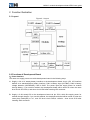
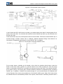
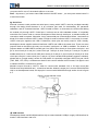
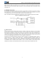
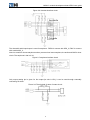
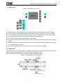
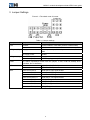
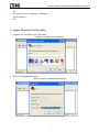
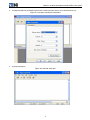
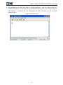
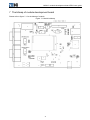
MG815+ module development board EBV3 user guide
ZTE MG815+ Module Development Board EBV3 User Guide
Version:V1.0
MG815+ module development board EBV3 user guide
Copyright Statement
Copyright © 2008 by ZTE Corporation
The copyright of this User Manual belongs to ZTE Corporation and under the protection of Copyright
Law of the People’s Republic of China and other relative laws.
No part of this publication may be excerpted,reproduced, translated or utilized in any form or by any
means (electronic or mechanical , including photocopying and microfilm) without prior written
permission from ZTE Corporation. Any violation behavior will be punished.
The information in the document is subject to change without notice. At the same time we reserve the
right to revise or recall the User Manual.
If there is anything unclear in this manual, please contact us or our agent or seller.
V4.9-TY, Feb.2008
1
MG815+ module development board EBV3 user guide
With strong technical force, ZTE Corporation can provide CDMA/GPRS module customers with the
following all-around technical support:
1. Provide complete technical documentation;
2. Provide the development board used for R&D, test, production, after-sales, etc.;
3. Provide evaluations and technical diagnosis for principle diagram, PCB, test scenarios;
4. Provide test environment;
ZTE Corporation provides customers with onsite supports, and also you could get supports through
telephone, website, instant communication, E-mail, etc.
The module website http://module.ztemt.com.cn provides the relevant industry information and module
technical documentation. The authorized module customers could download the latest technical
documentation for our website. If you have more requirements, you could send an E-mail to
[email protected]. You can also call us at 0755-86140899 for more supports.
2
MG815+ module development board EBV3 user guide
Foreword
Summary
The corresponding product name to this document is ZTE CDMA and GSM modules. It will be helpful
for you to understand how to use the development board by referring this document.
Readers
z
z
z
z
System designers
Hardware engineers
Software engineers
Test engineers
Brief
This document introduces how to use the development board, here is the index:
Chapter
Contents
1 summary
Characteristics, function chart and relevant technical
specifications of MG815+ module development board.
2 function illustration
Layout and functions.
3 jumper settings
Jumper settings of development board.
4 debugging and testing environment
Debugging and testing environment introduction.
5 debugging steps
Debugging steps introduction.
6 hyper terminal configuration
Hyper terminal configuration steps illustration.
7 The bitmap of module development board
The bitmap of module development board introduction.
Modification record
Document version V1.0 (2008-10-10)
The first time to publish in the form.
3
MG815+ module development board EBV3 user guide
Table of contents
1
2
3
4
5
6
7
Summary .........................................................................................................................................7
1.1 Characteristics of Development Board ......................................................................................7
1.2 Function Chart...........................................................................................................................7
1.3 Relative Documents ..................................................................................................................7
Function Illustration .........................................................................................................................8
2.1 Layout .......................................................................................................................................8
2.2 Functions of Development Board ..............................................................................................8
Jumper Settings ............................................................................................................................14
Debugging and Testing Environment.............................................................................................15
Debugging Steps ...........................................................................................................................15
Hyper Terminal Configuration ........................................................................................................17
The bitmap of module development board ....................................................................................20
4
MG815+ module development board EBV3 user guide
Table of figures
Figure 1-1 Function chart .......................................................................................................................7
Figure 2-1 Layout ...................................................................................................................................8
Figure 2-2 The principle of part of power................................................................................................9
Figure 2-3 The principle of reset and ON/OFF circuit.............................................................................9
Figure 2-4 level transfer circuit .............................................................................................................10
Figure 2-5 UIM/SIM card interface circuit .............................................................................................11
Figure 2-6 Handset interface circuit......................................................................................................12
Figure 2-7 earphone interface circuit....................................................................................................12
Figure 2-8 The principle of parts of output circuit .................................................................................12
Figure 2-9 The ketch map of LED ........................................................................................................13
Figure 2-10 The ketch map of testing sites...........................................................................................13
Figure 3-1 The sketch map of jumper...................................................................................................14
Figure 6-1 Create a new connection ....................................................................................................17
Figure 6-2 Setup corresponding serial port ..........................................................................................17
Figure 6-3 Configure serial port parameters.........................................................................................18
Figure 6-4 Activate serial port...............................................................................................................18
Figure 6-5 Ready to test .......................................................................................................................19
Figure 7-1 Module’s bitmap ..................................................................................................................20
5
MG815+ module development board EBV3 user guide
Tables
Table 3-1 Jumper settings ....................................................................................................................14
6
MG815+ module development board EBV3 user guide
1 Summary
1.1 Characteristics of Development Board
MG815EBV3 development board is designed for debugging and testing based on ZTE CDMA and
GSM modules. The users can debug above types of modules provided by ZTE with this board.
Meanwhile, considering the variety of modules, we designed jumpers on the development board
through which users could make the board work in different modes and therefore realize all the
functions provided by the module.
1.2 Function Chart
Basic functions provided by development board: power interface, serial port, UIM card interface, audio
interface, LED indicator, testing sites and so on. Please refer to the functions chart:
Figure 1-1 Function chart
1.3 Relative Documents
z
z
z
z
z
Module type selecting guide
《AT Command Manual for ZTE Corporation's MG815+ Module》
《AT Command Manual for ZTE Corporation's ME3000 Module》
《MG815+ Module Hardware Design User Manual》
《CDMA/GPRS module FAQ》
7
MG815+ module development board EBV3 user guide
2 Function Illustration
2.1 Layout
Figure 2-1 Layout
2.2 Functions of Development Board
1)Power Interface
The users can supply power to module development board in the following ways:
A) Supply a 3.8~4.2V steady battery interface to the development board via pin JP5. JP5 interface
defines as a standard lithium battery interface, PIN1 is battery input (VCCBAT), PIN3 is battery
voltage detection (BATSENSE), PIN5 is GND. The power input like supply power for module
through battery. If you use this method, the development board will be turned on when the users
short circuit JP5 PIN2,4, and short circuit JP30 after inserting JP5 connector.
B) Supply a 5~6V steady DC to the development board via pin JP20, which like supply power for
module through charger. If you use this method, the development board will be turned on when the
users place switch(S0) to “on” ,and JP5 short circuit PIN4,6(default),short circuit JP30 after
inserting JP20 connector.
8
MG815+ module development board EBV3 user guide
Figure 2-2 The principle of part of power
If user’s board has CPU, MCU and our module, you should advert to the order if module power first or
power at the same time. You should avoid module’s internal CMOS chip lanch-up, that will lead to the
module can’t start.
Press reset button (S3) on the development board to reset module. This button controls RESET pin on
module through a audion. Please refer to《MG815+ Module Hardware Design User Manual》for
information of Idiographic requirements to control RESET pin on modules.
Figure 2-3 The principle of reset and ON/OFF circuit
For the same reason, modules can be started or shut down by pressing switch button—press the
button to shut down when it powers on, press the button to run when it powers off. One end of this
switch is connected to ON/OFF pin on module, the other end connect with GND, The module’s ON/OFF
pin is used to pull up, low level is valid. Therefore ON/OFF operation is completed through controlling
ON/OFF pin. In addition, if ON/OFF the module through S1, you must disconnect JP4 (default short
circuit). Because JP4 is connect the module’s pin VCHG with 5~6VDC power. When JP4 is short circuit,
the module will turn on automatically if switch on the power, at this time S1 is inefficacy, because even if
9
MG815+ module development board EBV3 user guide
you press the S1 turn off, the module will turn on at once.
Note:At present ,if you want to start GSM module’s ON/OFF button,you must press switch button S1
to start the module.
2)Serial Port
External connector could provide two serial ports, among which UART1 must be provided externally
through the testing board because it is an exclusive port used for downloading, RF parameter
calibration, and AT command interface. UART1’s label is COM1. In most cases, the users would debug
the module only through UART1. Serial port 1 is always set as 8-line standard modem. It is specially
noted that if the users need to connect development board through serial port, a standard serial port
connection cable is required. Otherwise, it may cause serial port communication failure. Luminescence
diode D4 is used to indicate UART1’s state, D4 light is used to indicate UART1’s connection is normal.
UART2 uses pins together with USB. Furthermore, these pins are mainly used for USB. Actually,
development board supplies external interfaces UART2 and USB at the same time. There are some
jumpers fixed on the board, the users can choose if serial port 2 or USB is available. The location of
jumpers relation to USB/ UART2 are D20 (pin Com USB).If short circuit pin Com (short circuit pin 1 and
pin 2; short circuit pin 4 and pin 5; short circuit pin 7 and pin 8; short circuit pin 11 and pin 12) that is
enable serial port 2, If short circuit USB (short circuit pin 2 and pin 3; short circuit pin 5 and pin 6; short
circuit pin 8 and pin 9; short circuit pin 11 and pin 12), that is enable USB (software support is needed),
please refer to “jumper setting” section for D20 details. It is specially noted that UART2 only set 4 lines
(TXD, RXD, CTS, RTS). Luminescence diode D16 is used to indicate UART2’s state, D16 light is used
to indicate UART2’s connection is normal.
Module’s output IO level is 2.9VTTL, when it’s connect with standard 3.3V or 5V logic circuit (like
RS232 driver chip MAX3238 etc.), it need level transfer. Module’s output pin is connect with MAX3238
chip in our development board, and input pin is connect with MAX3238 through audion circuit in figure
2-4.
Figure 2-4 level transfer circuit
3)USB interface
Development board use MIC2550A interface chip to extend module’s USB pin, supply USB interface for
exterior. USB interface’s site is F4.
10
MG815+ module development board EBV3 user guide
Note: module’s USB pin and UART2 pin are in common use, so when you use USB, you need choose
jumper D20 short circuit USB pin (Short circuit pin2,3; Short circuit pin5,6; Short circuit pin8,9; Short
circuit pin11,12).
4)SIM/UIM Card Interfaces
As a standard communication module, this interface supports SIM and UIM at the same time. Testing
board supply UIM/SIM card. Because different card’s data pin’s output circuit is different, so I/O used
7.5K resistance pull up to VPP, and the location number of card interface is S2.
Note:be careful to insert the UIM/SIM card, metal piece is face to underside, jag is face to outside.
Figure 2-5 UIM/SIM card interface circuit
5)Audio Channels
External interface defines multiple audio channels, including 2 audio input channels, one for handset
and the other for earphone; 2 audio output channel, one for handset and the other for earphone too.
The interface also defines line output, used to support chord ring or voice output. All these audio
channels are extended from development board, if the users want to test their functions, they just need
to connect corresponding external devices, such as earphone, handset, etc.
Generally, the first audio input/output channel is used for handset, it is differential interface. HMIC is
connect with MIC_1, HSPK is connect with SPK_1. Considering handsets’ interfaces maybe are
different, so the design supplies two scheme: OldHandle and NewHandle, development board default
in initialization state. In different actual condition, user can choose whether to joint R46-52’s eight
resistances to decide to use NewHandle scheme or other custom scheme. Handset’s site is X5.
11
MG815+ module development board EBV3 user guide
Figure 2-6 Handset interface circuit
The channel2 audio input/output is used for earphone. FSPIN is connect with SPK_2, FMIC is connect
with module MIC_2.
Note:be careful to choose earphone socket,prevent when insert earphone, the audio and GND is short
circuit. The earphone’s site is is X1.
Figure 2-7 earphone interface circuit
Only output testing pin is given for line output (its site is JP3), it can be used through externally
connecting PA driver.
Figure 2-8 The principle of parts of output circuit
12
MG815+ module development board EBV3 user guide
6)LED Indicators
Figure 2-9 The ketch map of LED
Development board supply following LED to represent module’s state (software support is needed).
z D4: Serial port 1 working state indicator will be turned on when serial port1 connect successfully.
z D16: Serial port 2 working state indicator will be turned on when serial port2 connect successfully.
z D3: Call incoming/SMS indicator will be turned on when receive data.
z D5: Network state indicator will wink when inspect carrier.
z D7: module working state indicator will be turned on when module startup normally (2.85V output
power).
z D6: Development board power indicator will be turned on when development board power supply
(3.8V main power)normally.
z D21: module ringing indicator will be turned on when ringing signal is low level.
7)Testing Sites
The module’s 40-pin connector leads to 40 testing sites, which are provided for users to conveniently
test the module’s working status. The location number for test sites is X35.
Testing sites figure and the name of main testing sites signal are as follows:
Figure 2-10 The ketch map of testing sites
13
MG815+ module development board EBV3 user guide
3 Jumper Settings
Figure 3-1 The sketch map of jumper
Table 3-1 Jumper settings
Jumper
Jumper modes
Function explanation
JP2
Connect
Connect ON/OFF with GND (used for GSM module)
Disconnect
Default
Supply power
PIN1 is power input, PIN 3 is power detection, PIN 5 is
GND
No supply power
Default
Short circuit pin2,4
Supply power
Short circuit pin4,6
exterior supply power (default)
JP5(pin1,3,5)
JP5(pin2,4,6)
JP30
For reduce impedance arouse from the jumper, in fact, PCB has already short
circuited, but it’s inefficacy.
JP4
Short circuit
V_CHG enable (Default)
Disconnect
V_CHG inefficacy
Short circuit PIN1,2
Serial Port 2 RXD signal enable
Short circuit PIN4,5
Serial Port 2 RTS signal enable
Short circuit PIN7,8
Serial Port 2 CTS signal enable
Short circuit PIN10,11
Serial Port 2 TXD signal enable
Short circuit PIN2,3
USB_DATA signal enable
Short circuit PIN5,6
USB_VPO signal enable
Short circuit PIN8,9
USB_VMO signal enable
Short circuit PIN11,12
USB_OE signal enable
D20
14
MG815+ module development board EBV3 user guide
4 Debugging and Testing Environment
Debugging and testing environment is composed by development kit and PC. Development kit contains:
development board, module, linear power (typical output value is DC6V, 1500m A), standard 5-core
serial port cable, antenna, RF connection cable, handset, earphone. SIM/UIM card is necessary to
prepare.
The development board is used for power supply and signal output, linear power for supplying
necessary power to module (5V-7V) via development board, PC for inputting/outputting AT commands
from module via serial ports or USB interfaces. Please refer to practical design scheme of development
board for connecting structure.
5 Debugging Steps
Take CDMA module as an example:
1. Insert module to development board, connect power, serial port cable, antenna, handset, earphone
and SIM/UIM card. Then connect module with antenna through RF cable.
2. Turn on power, press S1 on-off. (If the JP4 is short circuit, neglect this step.)
3. Check current display. Current in module itself should be 80-100MA when power on. If current is too
low, please turn off power supply and check if connection between module and development board
is correct.
4. Open corresponding PC serial port( setting parameters:baud rate is 115200bps, 8 data bit, 1 stop
bit, no checkout, install USB to serial port converter before communicating through USB interface (if
necessary). Send “AT+CGMR” through serial port to query software version. response from
module:
+CGMR: S/W VER: M6025A-SBTW-3.1.30 ZDM1A4AAC0.11OK(indicates that software version is
M6025A-SBTW-3.1.30 ZDM1A4AAC0.11OK)
If software version query is on the rails, it makes out that the baseband portion of module works in
the right way. Otherwise, the connection on board or UART/USB interface must have some
mistakes.
5. Make sure that antenna can receive signals from base station through RF cable connecting module
with antenna.
Send “AT+CSQ? ” to query receiving signal’s intensity(RSSI)and frame error rate(FER).
response from module:
+CSQ:<RSSI>,<FER>
OK
(<RSSI>: virtual value:0-31, meanings of SQM(RSSI)are defined by manufacturer)
(<FER>: 99:return 99 if unknown)
RSSI value is determined by the signal intensity at the location of antenna. If RSSI is too low, please
check if there are some problems on the antenna. Keep moving antenna to the direction to base
station, and query signal intensity periodically, the RSSI should be rise up gradually.
Otherwise, the connection between module and antenna must be wrong
The environment of module working should basically be in gear after step 3, 4 are finished. You can
15
MG815+ module development board EBV3 user guide
test other functions by sending AT commands, such as audio output, call and response. Please
refer to《CDMA/GPRS module AT command manual》for details.
Convenient DEMO commands for testing working status of development board:
① After the board has been electrified for 5-6s, the display will be:
A、without SIM/UIM card:
+ZIND: 8
+ZIND: 0
B、with SIM/UIM card:
+ZIND: 8
+ZIND: 1
② Query ESN number of modules:(no card)
AT+GSN
+GSN: 698C4A4A
③ if SIM/UIM card and antenna has been planted, you can input commands below:
A、Query signal intensity(check if there is enough network signal)
AT+CSQ?
+CSQ: 20, 99
OK
B、Query network time(check if the right time could be captured)
AT+CCLK?
+CCLK: "04/04/10,00:08:39.038"
OK
④ input command below to dial:
A、dial out
ATD10010;
OK
+ZCORG:10010
+ZCCNT:0,3
B、ring off
ATH
OK
+ZCEND:29
⑤connect with handset and earphone, input audio channel query and switch commands below to
test if two audio channels are working correctly.
A、Channel query
AT+SPEAKER?
+SPEAKER: 0
16
MG815+ module development board EBV3 user guide
OK
B、channel switch(1-earphone,0-handset)
AT+SPEAKER=1;
OK
6 Hyper Terminal Configuration
1. Create a new connection, type in the name.
Figure 6-1 Create a new connection
2. Set up corresponding serial port.
Figure 6-2 Setup corresponding serial port
17
MG815+ module development board EBV3 user guide
3. Configure serial port parameters (baud rate, communication format, flow control and so on).
Figure 6-3 Configure serial port parameters
4. Activate serial port.
Figure 6-4 Activate serial port
18
MG815+ module development board EBV3 user guide
5. Use standard 9-core serial port cable to connect serial port 1 with PC, insert module and
antenna, and then turn on the switch on the development board. Type in “AT” and press enter on
the keyboard, if it responds “OK”, the configuration has been successful. You can use hyper
terminal to test.
Figure 6-5 Ready to test
19
MG815+ module development board EBV3 user guide
7 The bitmap of module development board
Please refer to figure 7-1 for the bitmap of module.
Figure 7-1 Module’s bitmap
20