1
GigaDevice Semiconductor Inc.
GD32F10x
ARM® Cortex™-M3 32-bit MCU
User Manual
GD32F10x User Manual
Table of Contents
Table of Contents ........................................................................................................... 1
List of Figures .............................................................................................................. 18
List of Tables ................................................................................................................ 26
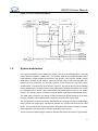
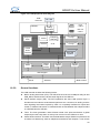
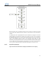
1. System and memory architecture ........................................................................ 30
1.1.
ARM Cortex-M3 processor .................................................................................................... 30
1.2.
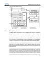
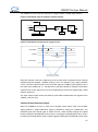
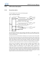
System architecture .............................................................................................................. 31
1.3.
Memory map ........................................................................................................................ 35
1.3.1.
Bit-banding ......................................................................................................................................... 38
1.3.2.
On-chip SRAM memory ................................................................................................................... 38
1.3.3.
On-chip Flash memory..................................................................................................................... 38
1.4.
Boot configuration ................................................................................................................ 39
1.5.
Device electronic signature ................................................................................................... 39
1.5.1.
Memory size information.................................................................................................................. 40
1.5.2.
Unique device ID (96 bits) ............................................................................................................... 40
1.6.
System configuration registers .............................................................................................. 41
2. Power control (PWR) ............................................................................................. 42
2.1.
Introduction .......................................................................................................................... 42
2.2.
Main features ....................................................................................................................... 42
2.3.
Function description ............................................................................................................. 42
2.3.1.
Battery Backup domain .................................................................................................................... 43
2.3.2.
VDD/VDDA power domain ................................................................................................................... 44
2.3.3.
1.2V power domain........................................................................................................................... 46
2.3.4.
Power saving modes ........................................................................................................................ 46
2.4.
PWR registers ....................................................................................................................... 48
2.4.1.
Power control register (PWR_CTLR)............................................................................................. 48
2.4.2.
Power status register (PWR_STR) ................................................................................................ 49
3. Flash Memory Controller (FMC)............................................................................ 51
3.1.
Introduction .......................................................................................................................... 51
3.2.
Main features ....................................................................................................................... 51
3.3.
Function description ............................................................................................................. 51
3.3.1.
Flash Memory Architecture.............................................................................................................. 51
3.3.2.
Read operations ................................................................................................................................ 52
3.3.3.
Unlock the FMC_CMR register ....................................................................................................... 52
1
GD32F10x User Manual
3.3.4.
Page Erase ........................................................................................................................................ 53
3.3.5.
Mass Erase ........................................................................................................................................ 54
3.3.6.
Main Flash Programming ................................................................................................................ 55
3.3.7.
Option bytes Erase ........................................................................................................................... 57
3.3.8.
Option bytes Programming.............................................................................................................. 57
3.3.9.
Option bytes Description.................................................................................................................. 58
3.3.10.
Page Erase/Program Protection ..................................................................................................... 59
3.3.11.
Security Protection ........................................................................................................................... 59
3.4.
FMC registers ........................................................................................................................ 60
3.4.1.
Flash reserved register (FMC_RESR) ........................................................................................... 60
3.4.2.
Flash unlock key register (FMC_UKEYR) ..................................................................................... 60
3.4.3.
Flash option byte operation unlock key register (FMC_OBKEYR) ............................................ 61
3.4.4.
Flash control/status register (FMC_CSR) ..................................................................................... 61
3.4.5.
Flash command register (FMC_CMR) ........................................................................................... 62
3.4.6.
Flash command address register (FMC_AR) ............................................................................... 63
3.4.7.
Flash option byte register (FMC_OPTR) ....................................................................................... 64
3.4.8.
Flash Page Erase/Program Protection register (FMC_WPR) .................................................... 64
3.4.9.
Flash unlock key register2 (FMC_UKEYR2) ................................................................................ 65
3.4.10.
Flash control/status register2 (FMC_CSR2) ................................................................................. 65
3.4.11.
Flash command register2 (FMC_CMR2) ...................................................................................... 66
3.4.12.
Flash command address register2 (FMC_AR2)........................................................................... 67
3.4.13.
Flash wait state control register (FMC_WSCR) ........................................................................... 67
3.4.14.
Flash Product reserved ID code register1 (FMC_RES_ID1) ..................................................... 68
3.4.15.
Flash Product reserved ID code register2 (FMC_RES_ID2) ..................................................... 68
4. Reset and clock control unit (RCC) ...................................................................... 70
Medium-, High- and X-density Reset and clock control unit (RCC) .................................................... 70
4.1.
Reset Control Unit (RCU) ....................................................................................................... 70
4.1.1.
Introduction ........................................................................................................................................ 70
4.1.2.
Function Description......................................................................................................................... 70
4.2.
Clock Control Unit (CCU) ....................................................................................................... 71
4.2.1.
Introduction ........................................................................................................................................ 71
4.2.2.
Main features ..................................................................................................................................... 73
4.2.3.
Function description ......................................................................................................................... 73
4.3.
RCC registers ......................................................................................................................... 76
4.3.1.
Global Clock control register (RCC_GCCR) ................................................................................. 76
4.3.2.
Global Clock configuration register (RCC_GCFGR) ................................................................... 77
4.3.3.
Global Clock interrupt register (RCC_GCIR) ................................................................................ 80
4.3.4.
APB2 Reset Control Register (RCC_APB2RCR) ........................................................................ 83
4.3.5.
APB1 Reset Control Register (RCC_APB1RCR) ........................................................................ 86
4.3.6.
AHB Clock Control Register (RCC_AHBCCR)............................................................................. 89
4.3.7.
APB2 Clock Control Register (RCC_APB2CCR)......................................................................... 90
2
GD32F10x User Manual
4.3.8.
APB1 clock Control Register (RCC_APB1CCR) ......................................................................... 92
4.3.9.
Backup Domain Control Register (RCC_BDCR) ......................................................................... 96
4.3.10.
Global Control/Status Register (RCC_GCSR) ............................................................................. 97
4.3.11.
RCC Deep-sleep mode voltage register (RCC_DEEPSLEEP_VC) .......................................... 99
Connectivity line devices: Reset and clock control unit (RCC) ......................................................... 100
4.4.
Reset Control Unit (RCU) ..................................................................................................... 100
4.4.1.
Introduction ...................................................................................................................................... 100
4.4.2.
Function Description....................................................................................................................... 100
4.5.
Clock Control Unit (CCU) ..................................................................................................... 101
4.5.1.
Introduction ...................................................................................................................................... 101
4.5.2.
Main features ................................................................................................................................... 103
4.5.3.
Function description ....................................................................................................................... 103
4.6.
RCC registers ....................................................................................................................... 106
4.6.1.
Global Clock control register (RCC_GCCR) ............................................................................... 106
4.6.2.
Global Clock configuration register (RCC_GCFGR) ................................................................. 108
4.6.3.
Global Clock interrupt register (RCC_GCIR) .............................................................................. 112
4.6.4.
APB2 Reset Control Register (RCC_APB2RCR) ...................................................................... 115
4.6.5.
APB1 Reset Control Register (RCC_APB1RCR) ...................................................................... 117
4.6.6.
AHB Clock Control Register (RCC_AHBCCR)........................................................................... 120
4.6.7.
APB2 Clock Control Register (RCC_APB2CCR)....................................................................... 122
4.6.8.
APB1 clock Control Register (RCC_APB1CCR) ....................................................................... 125
4.6.9.
Backup Domain Control Register (RCC_BDCR) ....................................................................... 128
4.6.10.
Global Control/Status Register (RCC_GCSR) ........................................................................... 129
4.6.11.
AHB Reset Control Register (RCC_AHBRCR) .......................................................................... 131
4.6.12.
Global Clock configuration register 2 (RCC_GCFGR2) ............................................................ 131
4.6.13.
RCC Deep-sleep mode voltage register (RCC_DEEPSLEEP_VC)........................................ 133
5. General-purpose and alternate-function I/Os .................................................... 135
5.1.
Introduction ........................................................................................................................ 135
5.2.
Main features ..................................................................................................................... 135
5.3.
Function description ........................................................................................................... 135
5.3.1.
GPIO pin configuration................................................................................................................... 136
5.3.2.
External interrupt/wakeup lines..................................................................................................... 137
5.3.3.
Input configuration .......................................................................................................................... 137
5.3.4.
Analog configuration....................................................................................................................... 138
5.3.5.
Output configuration ....................................................................................................................... 138
5.3.6.
Alternate functions (AF) ................................................................................................................. 139
5.4.
Remapping function I/O and debug configuration ............................................................... 144
5.4.1.
Introduction ....................................................................................................................................... 144
5.4.2.
Main features .................................................................................................................................... 144
5.4.3.
JTAG/SWD alternate function remapping.......................................................................................... 144
3
GD32F10x User Manual
5.4.4.
ADC AF remapping ........................................................................................................................ 145
5.4.5.
TIMER AF remapping .................................................................................................................... 146
5.4.6.
USART AF remapping ................................................................................................................... 148
5.4.7.
I2C1 AF remapping ........................................................................................................................ 148
5.4.8.
SPI1 AF remapping ........................................................................................................................ 148
5.4.9.
SPI3/I2S3 AF remapping ............................................................................................................... 149
5.4.10.
CAN1 AF remapping ...................................................................................................................... 149
5.4.11.
CAN2 AF remapping ...................................................................................................................... 149
5.4.12.
Ethernet alternate function remapping ........................................................................................ 150
5.4.13.
CLK pins AF remapping ................................................................................................................. 150
5.4.14.
GPIO locking function .................................................................................................................... 150
5.5.
GPIO registers ..................................................................................................................... 151
5.5.1.
GPIO port control register 1 (GPIOx_CTLR1) (x=A..F,G) ..................................................................... 151
5.5.2.
GPIO port control register 2 (GPIOx_CTLR2) (x=A..F,G) ..................................................................... 153
5.5.3.
GPIO port data input register (GPIOx_DIR) (x=A..F,G) ....................................................................... 154
5.5.4.
GPIO port data output register (GPIOx_DOR) (x=A..F,G) ................................................................... 155
5.5.5.
GPIO port bit operation register (GPIOx_BOR) (x=A..F,G) ................................................................. 156
5.5.6.
GPIO port bit clear register (GPIOx_BCR) (x=A..F,G) .......................................................................... 156
5.5.7.
GPIO port configuration lock register (GPIOx_LOCKR) (x=A,B) .......................................................... 157
5.5.8.
Event control register (AFIO_ECR) ..................................................................................................... 158
5.5.9.
AFIO port configuration register 1 (AFIO_PCFR1) .............................................................................. 158
5.5.10.
EXTI source selection register 1 (AFIO_ESSR1) .................................................................................. 165
5.5.11.
EXTI source selection register 2 (AFIO_ESSR2) .................................................................................. 166
5.5.12.
EXTI source selection register 3 (AFIO_ESSR3) .................................................................................. 166
5.5.13.
EXTI source selection register 4 (AFIO_ESSR4) .................................................................................. 167
5.5.14.
AFIO port configuration register 2 (AFIO_PCFR2) .............................................................................. 168
6. CRC Calculation Unit ........................................................................................... 170
6.1.
Introduction ........................................................................................................................ 170
6.2.
Main feature ....................................................................................................................... 170
6.3.
Function Description ........................................................................................................... 171
6.4.
CRC Register........................................................................................................................ 171
6.4.1.
CRC Data Register (CRC_DTR) .................................................................................................. 171
6.4.2.
CRC Free Data Register (CRC_FDTR) ...................................................................................... 172
6.4.3.
CRC Control Register (CRC_CTLR) ........................................................................................... 172
7. Interrupts and events .......................................................................................... 174
7.1.
Introduction ........................................................................................................................ 174
7.2.
Main features ..................................................................................................................... 174
7.3.
Function description ........................................................................................................... 174
7.3.1.
NVIC and exception/interrupt processing.................................................................................... 174
7.3.2.
External Interrupt and Event (EXTI) ............................................................................................. 179
4
GD32F10x User Manual
7.4.
EXTI registers ...................................................................................................................... 182
7.4.1.
Interrupt enable register (EXTI_IER) ........................................................................................... 182
7.4.2.
Event enable register (EXTI_EER) .............................................................................................. 182
7.4.3.
Rising edge trigger enable register (EXTI_RTE) ....................................................................... 183
7.4.4.
Falling edge trigger enable register (EXTI_FTE) ....................................................................... 183
7.4.5.
Software interrupt event register (EXTI_SIE) ............................................................................. 184
7.4.6.
Pending register (EXTI_PD).......................................................................................................... 184
8. Direct memory access controller (DMA) ............................................................ 185
8.1.
Introduction ........................................................................................................................ 185
8.2.
Main features ..................................................................................................................... 185
8.3.
Function description ........................................................................................................... 186
8.3.1.
DMA transfers .................................................................................................................................. 186
8.3.2.
Arbitration among channels .......................................................................................................... 187
8.3.3.
Next address generation algorithm .............................................................................................. 187
8.3.4.
Circulation mode ............................................................................................................................. 187
8.3.5.
Memory to memory mode.............................................................................................................. 187
8.3.6.
Interrupt requests ............................................................................................................................ 187
8.3.7.
DMA channel configuration procedure ........................................................................................ 188
8.3.8.
DMA Request Mapping .................................................................................................................. 188
8.4.
DMA registers ..................................................................................................................... 191
8.4.1.
DMA interrupt status register (DMA_IFR) ................................................................................... 191
8.4.2.
DMA interrupt flag clear register (DMA_ICR) ............................................................................. 192
8.4.3.
DMA channel x control register (DMA_CTLRx).......................................................................... 192
8.4.4.
DMA channel x remain counter (DMA_RCNTx) ......................................................................... 194
8.4.5.
DMA channel x peripheral base address register (DMA_PBARx)........................................... 194
8.4.6.
DMA channel x memory base address register (DMA_MBARx) ............................................. 195
9. Timer (TIMERx)..................................................................................................... 196
9.1.
Advanced timer (TIMER 1 and TIMER8) ............................................................................... 197
9.1.1.
Introduction ...................................................................................................................................... 197
9.1.2.
Main features ................................................................................................................................... 197
9.1.3.
Function description ....................................................................................................................... 197
9.1.4.
TIMER1 /TIMER8registers ............................................................................................................ 226
9.2.
General timers (TIMER2 to TIMER5) .................................................................................... 249
9.2.1.
Introduction ...................................................................................................................................... 249
9.2.2.
Main features ................................................................................................................................... 249
9.2.3.
Function description ....................................................................................................................... 249
9.2.4.
TIMER2 to TIMER5 registers ........................................................................................................ 270
9.3.
Basic timer (TIMER6 and TIMER7) ....................................................................................... 288
9.3.1.
Introduction ...................................................................................................................................... 288
9.3.2.
Main features ................................................................................................................................... 288
5
GD32F10x User Manual
9.3.3.
Function description ....................................................................................................................... 289
9.3.4.
TIMER6/7 registers......................................................................................................................... 291
9.4.
General timer (TIMER9 and TIMER12) ................................................................................. 295
9.4.1.
Introduction ...................................................................................................................................... 295
9.4.2.
Main features ................................................................................................................................... 295
9.4.3.
Function description ....................................................................................................................... 296
9.4.4.
TIMER9/TIMER12 registers .......................................................................................................... 319
9.5.
10.
General timer (TIMER10/11/13/14) .................................................................................... 330
9.5.1.
Introduction ...................................................................................................................................... 330
9.5.2.
Main features ................................................................................................................................... 331
9.5.3.
Function description ....................................................................................................................... 331
9.5.4.
TIMER10/11/13/14 registers ......................................................................................................... 347
Ethernet (ETH)................................................................................................... 356
10.1.
Introduction .................................................................................................................... 356
10.2.
Main features .................................................................................................................. 356
10.2.1.
Block Diagram ................................................................................................................................. 357
10.2.2.
MAC 802.3 Ethernet Packet.......................................................................................................... 358
10.2.3.
Ethernet pins ................................................................................................................................... 358
10.3.
Function description ........................................................................................................ 360
10.3.1.
Interface configuration.................................................................................................................... 360
10.3.2.
MAC .................................................................................................................................................. 364
10.3.3.
MAC statistics counters: MSC ...................................................................................................... 375
10.3.4.
Wake Up Management: WUM ...................................................................................................... 376
10.3.5.
Precision time protocol: PTP ......................................................................................................... 379
10.3.6.
DMA controller ................................................................................................................................. 383
10.3.7.
Ethernet interrupts .......................................................................................................................... 403
10.4.
Ethernet register descriptions .......................................................................................... 405
10.4.1.
Ethernet MAC configuration register (ETH_MAC_CFR) ........................................................... 405
10.4.2.
Ethernet MAC frame filter register (ETH_MAC_FRMFR) ......................................................... 407
10.4.3.
Ethernet MAC hash list high register (ETH_MAC_HLHR)........................................................ 409
10.4.4.
Ethernet MAC hash list low register (ETH_MAC_HLLR) .......................................................... 409
10.4.5.
Ethernet MAC PHY address register (ETH_MAC_PHYAR) ..................................................... 410
10.4.6.
Ethernet MAC MII data register (ETH_MAC_PHYDR) ............................................................. 411
10.4.7.
Ethernet MAC flow control register (ETH_MAC_FCTLR) ......................................................... 411
10.4.8.
Ethernet MAC flow control threshold register (ETH_MAC_FCTHR)....................................... 413
10.4.9.
Ethernet MAC VLAN tag register (ETH_MAC_VLTR) ............................................................... 414
10.4.10.
Ethernet MAC remote wakeup frame filter register (ETH_MAC_RWFFR) ........................ 414
10.4.11.
Ethernet MAC WUM register (ETH_MAC_WUMR) ............................................................... 415
10.4.12.
Ethernet MAC interrupt status register (ETH_MAC_ISR) .................................................... 416
10.4.13.
Ethernet MAC interrupt mask register (ETH_MAC_IMR) ..................................................... 417
10.4.14.
Ethernet MAC address 0 high register (ETH_MAC_ADDR0H) ........................................... 417
6
GD32F10x User Manual
10.4.15.
Ethernet MAC address 0 low register (ETH_MAC_ADDR0L) ............................................. 418
10.4.16.
Ethernet MAC address 1 high register (ETH_MAC_ADDR1H) ........................................... 418
10.4.17.
Ethernet MAC address1 low register (ETH_MAC_ADDR1L) .............................................. 419
10.4.18.
Ethernet MAC address 2 high register (ETH_MACADDR2H) ............................................. 419
10.4.19.
Ethernet MAC address 2 low register (ETH_MACADDR2L) ............................................... 420
10.4.20.
Ethernet MAC address 3 high register (ETH_MAC_ADDR3H) ........................................... 421
10.4.21.
Ethernet MAC address 3 low register (ETH_MAC_ADDR3L) ............................................. 421
10.4.22.
Ethernet MSC control register (ETH_MSC_CTLR) ............................................................... 422
10.4.23.
Ethernet MSC receive interrupt status register (ETH_MSC_RISR) .................................... 422
10.4.24.
Ethernet MSC transmit interrupt status register (ETH_MSC_TISR) ................................... 423
10.4.25.
Ethernet MSC receive interrupt mask register (ETH_MSC_RIMR) .................................... 424
10.4.26.
Ethernet MSC transmit interrupt mask register (ETH_MSC_TIMR) ................................... 425
10.4.27.
Ethernet MSC transmitted good frames after a single collision counter register
(ETH_MSC_SCCNT) ...................................................................................................................................... 426
10.4.28.
Ethernet MSC transmitted good frames after more than a single collision counter register
(ETH_MSC_MSCCNT) ................................................................................................................................... 426
10.4.29.
Ethernet MSC transmitted good frames counter register (ETH_MSC_TGFCNT) ............ 426
10.4.30.
Ethernet MSC received frames with CRC error counter register (ETH_MSC_RFCECNT)
427
10.4.31.
Ethernet MSC received frames with alignment error counter register
(ETH_MSC_RFAECNT) ................................................................................................................................. 427
10.4.32.
Ethernet MSC received good unicast frames counter register (ETH_MSC_RGUFCNT) 428
10.4.33.
Ethernet PTP time stamp control register (ETH_PTP_TSCTLR) ........................................ 428
10.4.34.
Ethernet PTP subsecond increment register (ETH_PTP_SSINCR) ................................... 429
10.4.35.
Ethernet PTP time stamp high register (ETH_PTP_TMSHR).............................................. 430
10.4.36.
Ethernet PTP time stamp low register (ETH_PTP_TMSLR) ................................................ 430
10.4.37.
Ethernet PTP time stamp high update register (ETH_PTP_TMSHUR) ............................. 430
10.4.38.
Ethernet PTP time stamp low update register (ETH_PTP_TMSLUR)................................ 431
10.4.39.
Ethernet PTP time stamp addend register (ETH_PTP_TSACNT) ...................................... 431
10.4.40.
Ethernet PTP expected time high register (ETH_PTP_ETHR)............................................ 432
10.4.41.
Ethernet PTP expected time low register (ETH_PTP_ETLR) .............................................. 432
10.4.42.
Ethernet DMA bus control register (ETH_DMA_BCR) .......................................................... 433
10.4.43.
Ethernet DMA transmit poll enable register (ETH_DMA_TPER)......................................... 434
10.4.44.
Ethernet DMA receive poll enable register (ETH_DMA_RPER) ......................................... 435
10.4.45.
Ethernet DMA receive descriptor table address register (ETH_DMA_RDTAR) ................ 435
10.4.46.
Ethernet DMA transmit descriptor table address register (ETH_DMATDTAR).................. 436
10.4.47.
Ethernet DMA status register (ETH_DMA_STR) ................................................................... 437
10.4.48.
Ethernet DMA control register (ETH_DMA_CTLR) ............................................................... 440
10.4.49.
Ethernet DMA interrupt enable register (ETH_DMA_IER) ................................................... 443
10.4.50.
Ethernet DMA missed frame and buffer overflow counter register (ETH_DMA_MFBOCNT)
445
10.4.51.
Ethernet DMA current transmit descriptor address register (ETH_DMA_CTDAR)........... 446
10.4.52.
Ethernet DMA current receive descriptor address register (ETH_DMA_CRDAR) ........... 447
10.4.53.
Ethernet DMA current transmit buffer address register (ETH_DMA_CTBAR) .................. 447
7
GD32F10x User Manual
10.4.54.
11.
Watchdog (WDG) .............................................................................................. 449
11.1.
Independent watchdog (IWDG) ....................................................................................... 449
11.1.1.
Introduction ...................................................................................................................................... 449
11.1.2.
Main features ................................................................................................................................... 449
11.1.3.
Function description ....................................................................................................................... 449
11.2.
IWDG registers ................................................................................................................ 451
11.2.1.
Control register (IWDG_CTLR)..................................................................................................... 451
11.2.2.
Prescaler register (IWDG_PSR) ................................................................................................... 451
11.2.3.
Reload register (IWDG_RLDR) .................................................................................................... 452
11.2.4.
Status register (IWDG_STR) ........................................................................................................ 453
11.3.
Window watchdog (WWDG) ............................................................................................ 453
11.3.1.
Introduction ...................................................................................................................................... 453
11.3.2.
Main features ................................................................................................................................... 453
11.3.3.
Function description ....................................................................................................................... 454
11.4.
12.
Ethernet DMA current receive buffer address register (ETH_DMA_CRBAR) ................... 447
WWDG registers .............................................................................................................. 455
11.4.1.
Control register (WWDG_CTLR) .................................................................................................. 455
11.4.2.
Configuration register (WWDG_CFR) ......................................................................................... 456
11.4.3.
Status register (WWDG_STR) ...................................................................................................... 457
Analog to Digital converter (ADC) ................................................................... 458
12.1.
Introduction .................................................................................................................... 458
12.2.
ADC main features........................................................................................................... 458
12.3.
ADC pins and internal signals........................................................................................... 458
12.4.
ADC function description ................................................................................................. 459
12.4.1
Calibration (ADC_CLB) .................................................................................................................. 459
12.4.2
ADC clock ........................................................................................................................................ 460
12.4.3
Regular and inserted channel groups .......................................................................................... 460
12.4.4
Conversion modes .......................................................................................................................... 460
12.4.5
Analog watchdog ............................................................................................................................ 463
12.4.6
Inserted channel management ..................................................................................................... 463
12.4.7
Data alignment ................................................................................................................................ 464
12.4.8
Programmable sample time .......................................................................................................... 464
12.4.9
External trigger ................................................................................................................................ 465
12.4.10
DMA request ................................................................................................................................ 466
12.4.11
Temperature sensor and internal reference voltage VREF .................................................. 466
12.4.12
ADC interrupts............................................................................................................................. 467
12.5.
Dual ADC mode ............................................................................................................... 467
12.5.1
Independent mode .......................................................................................................................... 468
12.5.2
Regular simultaneous mode ......................................................................................................... 468
12.5.3
Inserted simultaneous mode ......................................................................................................... 469
8
GD32F10x User Manual
12.5.4
Fast interleaved mode.................................................................................................................... 470
12.5.5
Slow interleaved mode................................................................................................................... 470
12.5.6
Alternate trigger mode.................................................................................................................... 471
12.5.7
Combined regular simultaneous + inserted simultaneous mode............................................. 472
12.5.8
Combined regular simultaneous + alternate trigger mode ....................................................... 472
12.5.9
Combined inserted simultaneous + interleaved mode .............................................................. 473
12.6.
13.
ADC registers ................................................................................................................... 473
12.6.1
ADC status register (ADC_STR) .................................................................................................. 473
12.6.2
ADC control register 1 (ADC_CTLR1) ......................................................................................... 474
12.6.3
ADC control register 2 (ADC_CTLR2) ......................................................................................... 476
12.6.4
ADC sample time register 1 (ADC_SPT1) .................................................................................. 479
12.6.5
ADC sample time register 2 (ADC_SPT2) .................................................................................. 479
12.6.6
ADC inserted channel data offset register x (ADC_ICOSx) (x=1..4)....................................... 480
12.6.7
ADC watchdog high threshold register (ADC_AWHT) .............................................................. 480
12.6.8
ADC watchdog low threshold register (ADC_AWLT)................................................................. 481
12.6.9
ADC regular sequence register 1 (ADC_RSQ1) ........................................................................ 481
12.6.10
ADC regular sequence register 2 (ADC_RSQ2) .................................................................... 481
12.6.11
ADC regular sequence register 3 (ADC_RSQ3) .................................................................... 482
12.6.12
ADC inserted sequence register (ADC_ISQ) ......................................................................... 482
12.6.13
ADC inserted data register x (ADC_IDTRx) (x= 1..4) ........................................................... 483
12.6.14
ADC regular data register (ADC_RDTR) ................................................................................ 483
Digital-to-analog converter (DAC) ................................................................... 485
13.1.
DAC introduction ............................................................................................................. 485
13.2.
DAC main features .......................................................................................................... 485
13.3.
DAC function description ................................................................................................. 486
13.3.1.
DAC channel enable .......................................................................................................................... 486
13.3.2.
DAC output buffer enable.................................................................................................................. 487
13.3.3.
DAC data format ................................................................................................................................ 487
13.3.4.
DAC conversion .................................................................................................................................. 487
13.3.5.
DAC output voltage ........................................................................................................................... 488
13.3.6.
DMA request ..................................................................................................................................... 488
13.3.7.
DAC trigger ........................................................................................................................................ 488
13.3.8.
Noise generation ............................................................................................................................... 489
13.3.9.
Trigangle-wave generation ................................................................................................................ 490
13.4.
Dual DAC channel conversion .......................................................................................... 491
13.4.1.
Independent trigger without wave generation ................................................................................. 492
13.4.2.
Independent trigger with same LFSR generation .............................................................................. 492
13.4.3.
Independent trigger with different LFSR gneneration ....................................................................... 492
13.4.4.
Independent trigger with same triangle generation ......................................................................... 493
13.4.5.
Independent trigger with different triangle generation .................................................................... 493
13.4.6.
Simultaneous software start.............................................................................................................. 494
9
GD32F10x User Manual
13.4.7.
Simultaneous trigger without wave generation ................................................................................ 494
13.4.8.
Simultaneous trigger with same LFSR generation ............................................................................. 494
13.4.9.
Simultaneous trigger with different LFSR generation ........................................................................ 494
13.4.10.
Simultaneous trigger with same triangle generation .................................................................... 495
13.4.11.
Simultaneous trigger with different triangle generation............................................................... 495
13.5.
14.
DAC registers................................................................................................................... 496
13.5.1.
DAC control register (DAC_CTLR)....................................................................................................... 496
13.5.2.
DAC software trigger register (DAC_SWTR) ....................................................................................... 499
13.5.3.
DAC channel1 12-bit right-aligned data holding register (DAC_C1R12DHR) .................................. 500
13.5.4.
DAC channel1 12-bit right-aligned data holding register (DAC_C1L12DHR)...................................... 500
13.5.5.
DAC channel1 8-bit right-aligned data holding register (DAC_C1R8DHR) ...................................... 501
13.5.6.
DAC channel2 12-bit right-aligned data holding register (DAC_C2R12DHR) ..................................... 501
13.5.7.
DAC channel2 12-bit left-aligned data holding register (DAC_C2L12DHR) ........................................ 502
13.5.8.
DAC channel2 8-bit right-aligned data holding register (DAC_C2R8DHR) ......................................... 502
13.5.9.
Dual DAC 12-bit right-aligned data holding register (DAC_DCR12DHR) ............................................ 503
13.5.10.
Dual DAC 12-bit left-aligned data holding register (DAC_DCL12DHR) .......................................... 503
13.5.11.
Dual channel2 8-bit right-aligned data holding register (DAC_DCR8DHR) .................................... 504
13.5.12.
DAC channel1 output data register (DAC_C1ODR) ........................................................................ 504
13.5.13.
DAC channel2 output data register (DAC_C2ODR) ........................................................................ 505
Inter-integrated circuit (I2C) interface ............................................................. 506
14.1.
Introduction .................................................................................................................... 506
14.2.
Main features .................................................................................................................. 506
14.3.
Function description ........................................................................................................ 506
14.3.1.
SDA and SCL lines ......................................................................................................................... 507
14.3.2.
Data validation................................................................................................................................. 508
14.3.3.
Start and stop condition ................................................................................................................. 508
14.3.4.
Clock synchronization .................................................................................................................... 508
14.3.5.
Arbitration ......................................................................................................................................... 509
14.3.6.
I2C communication flow ................................................................................................................. 510
14.3.7.
Programming model ....................................................................................................................... 511
14.3.8.
Packet error checking .................................................................................................................... 521
14.3.9.
SMBus support................................................................................................................................ 521
14.3.10.
14.4.
Status, errors and interrupts ..................................................................................................... 522
I2C registers..................................................................................................................... 523
14.4.1.
I2C control register 1 (I2C_CTLR1) ............................................................................................. 523
14.4.2.
I2C control register 2 (I2C_CTLR2) ............................................................................................. 524
14.4.3.
I2C own address register 1 (I2C_AR1)........................................................................................ 525
14.4.4.
I2C own address register 2 (I2C_AR2)........................................................................................ 526
14.4.5.
I2C transfer buffer register (I2C_DTR) ........................................................................................ 526
14.4.6.
I2C transfer status register 1 (I2C_STR1) .................................................................................. 527
14.4.7.
I2C transfer status register 2 (I2C_STR2) .................................................................................. 529
10
GD32F10x User Manual
15.
14.4.8.
I2C clock configure register (I2C_CLKR) .................................................................................... 530
14.4.9.
I2C Rise Time register (I2C_RTR) ............................................................................................... 530
Serial peripheral interface / Inter-IC sound (SPI/I2S) ..................................... 531
15.1.
Introduction .................................................................................................................... 531
15.2.
Main features .................................................................................................................. 531
15.2.1.
SPI features ..................................................................................................................................... 531
15.2.2.
I2S features ..................................................................................................................................... 532
15.3.
SPI function description................................................................................................... 533
15.3.1.
Pin configuration ............................................................................................................................. 533
15.3.2.
SPI slave mode ............................................................................................................................... 535
15.3.3.
SPI master mode ............................................................................................................................ 536
15.3.4.
SPI simplex communication .......................................................................................................... 537
15.3.5.
Data Rx and Tx procedures .......................................................................................................... 537
15.3.6.
CRC calculation .............................................................................................................................. 538
15.3.7.
Status flags and error flags ........................................................................................................... 539
15.3.8.
Disabling the SPI ............................................................................................................................ 540
15.3.9.
DMA requests .................................................................................................................................. 541
15.3.10.
15.4.
I2S function description ................................................................................................... 543
15.4.1.
General description ........................................................................................................................ 543
15.4.2.
Supported audio standards ........................................................................................................... 544
15.4.3.
Clock generator ............................................................................................................................... 551
15.4.4.
Operation ......................................................................................................................................... 554
15.4.5.
DMA features ................................................................................................................................... 558
15.5.
16.
SPI interrupts............................................................................................................................... 542
SPI registers ..................................................................................................................... 559
15.5.1.
SPI control register 1 (SPI_CTLR1) ............................................................................................. 559
15.5.2.
SPI control register 2 (SPI_CTLR2) ............................................................................................. 560
15.5.3.
SPI status register (SPI_STR) .............................................................................................................. 561
15.5.4.
SPI data register (SPI_DTR) ......................................................................................................... 563
15.5.5.
SPI CRC polynomial register (SPI_CPR).................................................................................... 563
15.5.6.
SPI RX CRC register (SPI_RCR) ................................................................................................. 563
15.5.7.
SPI TX CRC register (SPI_TCR) .................................................................................................. 564
15.5.8.
SPI I2S control register (SPI_I2SCTLR) ..................................................................................... 564
15.5.9.
SPI I2S clock prescaler register (SPI_I2SCKP) ......................................................................... 566
Backup registers (BKP) .................................................................................... 567
16.1.
Introduction .................................................................................................................... 567
16.2.
Main features .................................................................................................................. 567
16.3.
Function description ........................................................................................................ 567
16.3.1.
RTC clock calibration ..................................................................................................................... 567
16.3.2.
Tamper detection ............................................................................................................................ 567
11
GD32F10x User Manual
16.4.
17.
BKP registers ................................................................................................................... 568
16.4.1.
Backup data register x (BKP_DRx) (x= 1..42) ............................................................................ 568
16.4.2.
RTC clock calibration register (BKP_RCCR) .............................................................................. 568
16.4.3.
Tamper pin control register (BKP_TPCR) ................................................................................... 569
16.4.4.
Tamper interrupt event register (BKP_TIER) .............................................................................. 569
Universal synchronous asynchronous receiver transmitter (USART) ......... 571
17.1.
Introduction .................................................................................................................... 571
17.2.
Main features .................................................................................................................. 571
17.3.
Function description ........................................................................................................ 572
17.3.1.
USART transmitter.......................................................................................................................... 573
17.3.2.
USART receiver .............................................................................................................................. 574
17.3.3.
Reception errors ............................................................................................................................. 575
17.3.4.
Baud rate generation ...................................................................................................................... 575
17.3.5.
Multi-processor communication .................................................................................................... 575
17.3.6.
LIN mode.......................................................................................................................................... 576
17.3.7.
Half-duplex communication mode ................................................................................................ 576
17.3.8.
Synchronous mode......................................................................................................................... 577
17.3.9.
Smartcard (ISO7816) mode .......................................................................................................... 578
17.3.10.
IrDA SIR ENDEC mode ............................................................................................................. 579
17.3.11.
Hardware flow control ................................................................................................................ 580
17.3.12.
DMA requests .............................................................................................................................. 581
17.3.13.
USART interrupts ........................................................................................................................ 582
17.4.
18.
USART registers ............................................................................................................... 583
17.4.1.
USART status register (USART_STR) ........................................................................................ 583
17.4.2.
USART data register (USART_DR) ............................................................................................. 585
17.4.3.
USART baud rate register (USART_BRR).................................................................................. 586
17.4.4.
USART control register 1 (USART_CTLR1) ............................................................................... 586
17.4.5.
USART control register 2 (USART_CTLR2) ............................................................................... 588
17.4.6.
USART control register 3 (USART_CTLR3) ............................................................................... 589
17.4.7.
USART guard time and prescaler register (USART_GTPR) .................................................... 591
MCU Debug (MCUDBG) .................................................................................... 592
18.1.
Introduction .................................................................................................................... 592
18.2.
Function description ........................................................................................................ 592
18.2.1.
Debug support for low-power mode ............................................................................................. 592
18.2.2.
Debug support for timer, i2c,bxCAN, wwdg and iwdg ............................................................... 592
18.3.
19.
MCUDBG registers ........................................................................................................... 592
18.3.1.
MCUDBG ID code register (MCUDBG_IDR).............................................................................. 592
18.3.2.
MCUDBG control register (MCUDBG_CTLR) ............................................................................ 593
Universal serial bus full-speed device interface (USB 2.0 FS)...................... 597
19.1.
Introduction .................................................................................................................... 597
12
GD32F10x User Manual
19.2.
Main features .................................................................................................................. 597
19.3.
Implementation .............................................................................................................. 598
19.4.
Signal Description............................................................................................................ 598
19.5.
Function description ........................................................................................................ 598
19.5.1.
Block Diagram ................................................................................................................................. 598
19.5.2.
General functions ............................................................................................................................ 599
19.5.3.
Operation procedure ...................................................................................................................... 600
19.5.4.
USB Interrupts ................................................................................................................................. 604
19.5.5.
Isochronous transfers..................................................................................................................... 605
19.5.6.
Reset events.................................................................................................................................... 605
19.5.7.
Suspend/Resume events .............................................................................................................. 606
19.6.
USB registers ................................................................................................................... 606
19.6.1.
USB control register (USB_CTLR) ............................................................................................... 606
19.6.2.
USB interrupt Flag register (USB_IFR) ....................................................................................... 608
19.6.3.
USB Status register (USB_SR) .................................................................................................... 609
19.6.4.
USB device address register (USB_AR) ..................................................................................... 609
19.6.5.
USB Buffer address register (USB_BAR) ................................................................................... 610
19.6.6.
USB endpoint n control/status register (USB_EPnCSR), n=[0..7] .......................................... 610
19.6.7.
USB Transmission buffer address register n (USB_TXARn) ................................................... 612
19.6.8.
USB Transmission byte count register n (USB_TXCNTn)........................................................ 612
19.6.9.
USB Reception buffer address register n (USB_RXARn) ........................................................ 613
19.6.10.
20.
USB Reception byte count register n (USB_RXCNTRn)...................................................... 613
Real-time Clock(RTC) ....................................................................................... 614
20.1.
Introduction .................................................................................................................... 614
20.2.
Main feature ................................................................................................................... 614
20.3.
Function Description ....................................................................................................... 615
20.3.1.
RTC overview .................................................................................................................................. 615
20.3.2.
RTC reset ......................................................................................................................................... 615
20.3.3.
RTC reading .................................................................................................................................... 616
20.3.4.
RTC configuration ........................................................................................................................... 616
20.3.5.
RTC flag assertion .......................................................................................................................... 616
20.4.
RTC Register .................................................................................................................... 617
20.4.1.
RTC control register1(RTC_CTLR1) ............................................................................................ 617
20.4.2.
RTC control register2(RTC_CTLR2) ............................................................................................ 618
20.4.3.
RTC prescaler load register1 (RTC_PLR1) ................................................................................ 619
20.4.4.
RTC prescaler load register2(RTC_PLR2) ................................................................................. 619
20.4.5.
RTC prescaler divider register1 (RTC_PREDIV1) ..................................................................... 620
20.4.6.
RTC prescaler divider register2 (RTC_PREDIV2) ..................................................................... 620
20.4.7.
RTC counter register1(RTC_CNT1)............................................................................................. 620
20.4.8.
RTC counter register2 (RTC_CNT2) ........................................................................................... 621
13
GD32F10x User Manual
RTC alarm register1(RTC_ALRMR1) .......................................................................................... 621
20.4.9.
20.4.10.
21.
RTC alarm register2 (RTC_ALAMR2) ..................................................................................... 621
External memory controller (EXMC) ............................................................... 622
21.1.
Introduction .................................................................................................................. 622
21.2.
Main feature ................................................................................................................. 622
21.3.
Function description .................................................................................................. 623
21.3.1.
EXMC Architecture ......................................................................................................................... 623
21.3.2.
Basic regulation of EXMC access ................................................................................................ 623
21.3.3.
External device address mapping ................................................................................................ 624
21.3.4.
NOR Flash/PSRAM controller....................................................................................................... 628
21.3.5.
Nand Flash or PC Card controller ................................................................................................ 647
21.4.
22.
EXMC registers ............................................................................................................ 651
21.4.1.
NOR/PSRAM controller registers ................................................................................................. 651
21.4.2.
NAND Flash/PC card controller registers.................................................................................... 656
Controller Area Network (bxCAN) ................................................................... 662
22.1.
Introduction .................................................................................................................... 662
22.2.
Main features .................................................................................................................. 662
22.3.
Function description ........................................................................................................ 663
22.3.1.
Working mode ................................................................................................................................. 663
22.3.2.
Communication modes .................................................................................................................. 664
22.3.3.
Data transmission ........................................................................................................................... 665
22.3.4.
Data reception ................................................................................................................................. 667
22.3.5.
Filtering Function ............................................................................................................................ 669
22.3.6.
Time-triggered communication ..................................................................................................... 671
22.3.7.
Communication parameters .......................................................................................................... 672
22.3.8.
Error flags ........................................................................................................................................ 674
22.3.9.
bxCAN interrupts............................................................................................................................. 674
22.4.
bxCAN registers ............................................................................................................... 675
22.4.1.
CAN control register (CAN_CTLR) .............................................................................................. 675
22.4.2.
CAN status register (CAN_STR) .................................................................................................. 677
22.4.3.
CAN transmit status register (CAN_TSTR) ................................................................................ 678
22.4.4.
CAN receive FIFO0 register (CAN_RFR0) ................................................................................. 680
22.4.5.
CAN receive FIFO1 register (CAN_RFR1) ................................................................................. 680
22.4.6.
CAN interrupt enable register (CAN_IER) .................................................................................. 681
22.4.7.
CAN error register (CAN_ER) ....................................................................................................... 683
22.4.8.
CAN bit timing register (CAN_BTR) ............................................................................................. 684
22.4.9.
CAN transmit mailbox identifier register (CAN_TMIRx) (x=0..2) ............................................. 685
22.4.10.
CAN transmit mailbox property register (CAN_TMPRx) (x=0..2) ........................................ 685
22.4.11.
CAN transmit mailbox data0 register (CAN_TMD0Rx) (x=0..2) .......................................... 686
22.4.12.
CAN transmit mailbox data1 register (CAN_TMD1Rx) (x=0..2) .......................................... 687
14
GD32F10x User Manual
23.
22.4.13.
CAN receive FIFO mailbox identifier register (CAN_RFMIRx) (x=0..1) ............................. 687
22.4.14.
CAN receive FIFO mailbox property register (CAN_RFMPRx) (x=0..1) ............................ 688
22.4.15.
CAN receive FIFO mailbox data0 register (CAN_RFMD0Rx) (x=0..1)............................... 688
22.4.16.
CAN receive FIFO mailbox data1 register (CAN_RFMD1Rx) (x=0..1)............................... 689
22.4.17.
CAN filter control register (CAN_FCTLR) ............................................................................... 689
22.4.18.
CAN filter mode register (CAN_FMR) ..................................................................................... 690
22.4.19.
CAN filter scale register (CAN_FSR) ....................................................................................... 691
22.4.20.
CAN filter associated FIFO register (CAN_FAFR)................................................................. 691
22.4.21.
CAN filter working register (CAN_FWR) ................................................................................. 691
22.4.22.
CAN filter x data y register (CAN_FxDyR) (x=0..27, y=0..1) ................................................ 692
Secure digital input/output interface (SDIO) .................................................. 693
23.1.
SDIO main features.......................................................................................................... 693
23.2.
SDIO bus topology ........................................................................................................... 693
23.3.
SDIO functional description ............................................................................................. 696
23.3.1.
SDIO adapter................................................................................................................................... 697
23.3.2.
AHB interface .................................................................................................................................. 698
23.3.3.
SDIO state machine ....................................................................................................................... 699
23.4.
Card functional description ............................................................................................. 702
23.4.1.
Card registers .................................................................................................................................. 702
23.4.2.
Commands ...................................................................................................................................... 703
23.4.3.
Responses ....................................................................................................................................... 714
23.4.4.
Two status fields of the card.......................................................................................................... 717
23.5.
Programming sequence ................................................................................................... 724
23.5.1.
Card identification ........................................................................................................................... 724
23.5.2.
No Data Commands ....................................................................................................................... 726
23.5.3.
Single Block or Multiple Block write ............................................................................................. 726
23.5.4.
Single Block or Multiple Block read .............................................................................................. 728
23.5.5.
Stream write and Stream read (MMC only) ................................................................................ 729
23.5.6.
Erase ................................................................................................................................................ 730
23.5.7.
Bus width selection ......................................................................................................................... 731
23.5.8.
Protection management................................................................................................................. 731
23.5.9.
Card Lock/Unlock Operation ......................................................................................................... 732
23.6.
Specific operations .......................................................................................................... 734
23.6.1.
SD I/O specific operations ............................................................................................................. 734
23.6.2.
CE-ATA specific operations ........................................................................................................... 738
23.7.
HW flow control .............................................................................................................. 739
23.8.
SDIO registers .................................................................................................................. 739
23.8.1.
SDIO power register (SDIO_POWER) ........................................................................................ 739
23.8.2.
SDIO clock control register (SDIO_CLKCTLR) .......................................................................... 739
23.8.3.
SDIO parameter register (SDIO_PARA) ..................................................................................... 740
15
GD32F10x User Manual
24.
23.8.4.
SDIO command register (SDIO_CMD)........................................................................................ 741
23.8.5.
SDIO command response register (SDIO_RESPCMD) ........................................................... 742
23.8.6.
SDIO response register (SDIO_RESPx x=1-4) .......................................................................... 742
23.8.7.
SDIO data timeout register (SDIO_DTTR).................................................................................. 743
23.8.8.
SDIO data length register (SDIO_DTLEN) ................................................................................. 743
23.8.9.
SDIO data control register (SDIO_DTCTLR).............................................................................. 744
23.8.10.
SDIO data counter register (SDIO_DTCNT) .......................................................................... 746
23.8.11.
SDIO status register (SDIO_STR) ........................................................................................... 746
23.8.12.
SDIO interrupt clear register (SDIO_ICR) ............................................................................... 748
23.8.13.
SDIO interrupt enable register (SDIO_IER)............................................................................ 749
23.8.14.
SDIO FIFO counter register (SDIO_FIFOCNT) ..................................................................... 751
23.8.15.
SDIO FIFO data register (SDIO_FIFO) ................................................................................... 751
Universal serial bus on-the-go Full-Speed interface (USB OTG_FS) ........... 752
24.1.
Introduction .................................................................................................................... 752
24.2.
Main features .................................................................................................................. 752
24.2.1.
General features ............................................................................................................................. 752
24.2.2.
Host-mode features ........................................................................................................................ 753
24.2.3.
Device-mode features .................................................................................................................... 753
24.3.
Function description ........................................................................................................ 754
24.3.1.
USB 2.0 OTG Full-Speed core ..................................................................................................... 754
24.3.2.
OTG Full-Speed PHY..................................................................................................................... 755
24.4.
OTG_FS operation............................................................................................................ 755
24.4.1.
OTG mode ....................................................................................................................................... 756
24.4.2.
Host mode........................................................................................................................................ 757
24.4.3.
Peripheral mode .............................................................................................................................. 763
24.5.
USB OTG_FS FIFO ............................................................................................................. 767
24.5.1.
Host FIFO architecture................................................................................................................... 768
24.5.2.
Peripheral FIFO architecture ......................................................................................................... 770
24.5.3.
FIFO RAM allocation ...................................................................................................................... 771
24.6.
SOF trigger ...................................................................................................................... 773
24.6.1.
Host SOFs ....................................................................................................................................... 774
24.6.2.
Peripheral SOFs ............................................................................................................................. 774
24.7.
Power options ................................................................................................................. 774
24.8.
OTG_FS interrupts ........................................................................................................... 775
24.9.
USB system performance ................................................................................................. 776
24.10.
OTG_FS registers ............................................................................................................. 777
24.10.1.
OTG_FSRs memory map.......................................................................................................... 778
24.10.2.
USB OTG_FS global registers ................................................................................................. 778
24.10.3.
Host control and status registers .............................................................................................. 802
24.10.4.
Device control and status registers .......................................................................................... 814
16
GD32F10x User Manual
24.10.5.
OTG_FS Power and clock control register (OTG_FS_PCCTLR) ....................................... 840
17
GD32F10x User Manual
List of Figures
Figure 1-1 Cortex™-M3 block diagram ............................................................................................. 31
Figure 1-2 GD32F10x Medium-density series system architecture ........................................... 32
Figure 1-3 GD32F10x High-density series system architecture ................................................. 33
Figure 1-4 GD32F10x Extra-density series system architecture ................................................ 34
Figure 1-5 GD32F10x Connectivity line series system architecture ......................................... 35
Figure 1-6 GD32F10x memory map.................................................................................................... 37
Figure 2-1 Power supply overview ..................................................................................................... 43
Figure 2-2 Waveform of the POR/PDR .............................................................................................. 45
Figure 2-3 Waveform of the LVD threshold ..................................................................................... 45
Figure 4-1 the system reset circuit .................................................................................................... 71
Figure 4-2 the system reset circuit .................................................................................................. 101
Figure 5-1 The basic structure of standard I/O Port bit and five-volt tolerant I/O Port bit 136
Figure 5-2 Input floating/pull up/pull down configurations of I/O Port bit ............................. 137
Figure 5-3 Analog configuration of I/O Port bit............................................................................. 138
Figure 5-4 The Output configuration of I/O Port bit ..................................................................... 139
Figure 5-5 The Alternate Function configuration of I/O Port bit ............................................... 140
Figure 6-1 Block Diagram of CRC Calculation Unit ..................................................................... 171
Figure 7-1 Block diagram of EXTI ..................................................................................................... 180
Figure 8-1 DMA interrupt generation logic ..................................................................................... 188
Figure 8-2 DMA1 request mapping .................................................................................................. 189
Figure 8-3 DMA1 request mapping .................................................................................................. 190
Figure 9-1 Advanced timer block diagram ..................................................................................... 198
Figure 9-2 Counter timing diagram with prescaler division change from 1 to 2.................. 198
Figure 9-3 Counter timing diagram with prescaler division change from 1 to 4.................. 199
Figure 9-4 Counter timing diagram, internal clock divided by 1 .............................................. 200
Figure 9-5 Counter timing diagram, internal clock divided by 2 .............................................. 200
Figure 9-6 Counter timing diagram, internal clock divided by 4 .............................................. 201
Figure 9-7 Counter timing diagram, internal clock divided by N ............................................. 201
Figure 9-8 Counter timing diagram, update event when ARSE=0 ........................................... 202
Figure 9-9 Counter timing diagram, update event when ARSE=1 ........................................... 202
Figure 9-10 Counter timing diagram, internal clock divided by 1 ............................................ 203
Figure 9-11 Counter timing diagram, internal clock divided by 2 ............................................ 204
Figure 9-12 Counter timing diagram, internal clock divided by 4 ............................................ 204
Figure 9-13 Counter timing diagram, internal clock divided by N ........................................... 205
Figure 9-14 Counter timing diagram, update event when repetition counter is not used . 205
Figure 9-15 Counter timing diagram, internal clock divided by 1, TIMERx_CARL=0x5 ..... 206
Figure 9-16 Counter timing diagram, internal clock divided by 1 ............................................ 207
Figure 9-17 Counter timing diagram, internal clock divided by 1, TIMERx_CARL=0x5 ..... 207
Figure 9-18 Counter timing diagram, internal clock divided by N ........................................... 208
18
GD32F10x User Manual
Figure 9-19 Counter timing diagram, update event with ARSE=1(counter underflow) ...... 208
Figure 9-20 Counter timing diagram, Update event with ARSE=1 (counter overflow) ....... 209
Figure 9-21 Update rate examples depending on mode and TIMERx_CREP........................ 210
Figure 9-22 Control circuit in normal mode, internal clock divided by 1 ............................... 210
Figure 9-23 Capture/compare channel (example: channel 1 input stage) ............................. 212
Figure 9-24 Capture/compare channel 1 main circuit ................................................................. 213
Figure 9-25 Output stage of capture/compare channel (channel 1 to 3) ................................ 213
Figure 9-26 Output stage of capture/compare channel (channel 4) ........................................ 214
Figure 9-27 Output compare mode, toggle on OC1 ..................................................................... 214
Figure 9-28 Complementary output with dead-time insertion. ................................................. 215
Figure 9-29 Dead-time waveforms with delay greater than the negative pulse ................... 216
Figure 9-30 Dead-time waveforms with delay greater than the positive pulse .................... 216
Figure 9-31 Output behavior in response to a break(The break input is acting on high level)
........................................................................................................................................................... 217
Figure 9-32 Single pulse mode ......................................................................................................... 218
Figure 9-33 Example of counter operation in encoder interface mode .................................. 219
Figure 9-34 Example of encoder interface mode with TI1FP1 polarity inverted .................. 219
Figure 9-35 Control circuit in restart mode.................................................................................... 220
Figure 9-36 Control circuit in pause mode .................................................................................... 221
Figure 9-37 Control circuit in trigger mode ................................................................................... 221
Figure 9-38 Timer1 Master/Slave mode timer example ............................................................... 222
Figure 9-39 Triggering timer 1 with Enable of timer 2 ................................................................. 223
Figure 9-40 Triggering timer 1 with update of timer 2 ................................................................. 224
Figure 9-41 Gating timer 1 with enable of timer 2 ........................................................................ 224
Figure 9-42 Gating timer 1 with OC1REF of timer 2..................................................................... 225
Figure 9-43 Triggering timer 1 and timer2 with timer2’s TI1 input ........................................... 226
Figure 9-44 General timer block diagram(TIMER2 to TIMER5) ................................................. 250
Figure 9-45 Counter timing diagram with prescaler division change from 1 to 2 ............... 250
Figure 9-46 Counter timing diagram with prescaler division change from 1 to 4 ............... 251
Figure 9-47 Counter timing diagram, internal clock divided by 1 ............................................ 252
Figure 9-48 Counter timing diagram, internal clock divided by 2 ............................................ 252
Figure 9-49 Counter timing diagram, internal clock divided by 4 ............................................ 253
Figure 9-50 Counter timing diagram, internal clock divided by N ........................................... 253
Figure 9-51 Counter timing diagram, update event when ARSE=0 ......................................... 254
Figure 9-52 Counter timing diagram, update event when ARSE=1 ......................................... 254
Figure 9-53 Counter timing diagram, internal clock divided by 1 ............................................ 255
Figure 9-54 Counter timing diagram, internal clock divided by 2 ............................................ 256
Figure 9-55 Counter timing diagram, internal clock divided by 4 ............................................ 256
Figure 9-56 Counter timing diagram, internal clock divided by N ........................................... 257
Figure 9-57 Counter timing diagram, update event ..................................................................... 257
Figure 9-58 Counter timing diagram, internal clock divided by 1, TIMERx_CARL = 0x5 ... 258
Figure 9-59 Counter timing diagram, internal clock divided by 2 ............................................ 259
Figure 9-60 Counter timing diagram, internal clock divided by 4, TIMERx_CARL=0x63 ... 259
Figure 9-61 Counter timing diagram, internal clock divided by N ........................................... 260
19
GD32F10x User Manual
Figure 9-62 Counter timing diagram, update event with ARSE=1(counter underflow) ...... 260
Figure 9-63 Counter timing diagram, Update event with ARSE=1 (counter overflow) ....... 261
Figure 9-64 Control circuit in normal mode, internal clock divided by 1 ............................... 262
Figure 9-65 Capture/compare channel (example: channel 1 input stage) ............................. 263
Figure 9-66 Capture/compare channel 1 main circuit ................................................................. 264
Figure 9-67 Output stage of capture/compare channel (channel 1) ........................................ 264
Figure 9-68 Output compare mode, toggle on OC1 ..................................................................... 265
Figure 9-69 Single pulse mode ......................................................................................................... 266
Figure 9-70 Example of counter operation in encoder interface mode .................................. 267
Figure 9-71 Example of encoder interface mode with TI1FP1 polarity inverted .................. 268
Figure 9-72 Control circuit in restart mode.................................................................................... 268
Figure 9-73 Control circuit in pause mode .................................................................................... 269
Figure 9-74 Control circuit in trigger mode ................................................................................... 269
Figure 9-75 Master/Slave mode timer example ............................................................................. 270
Figure 9-76 General timer block diagram (TIMER6 and TIMER7) ............................................. 289
Figure 9-77 Counter timing diagram with prescaler division change from 1 to 2 ............... 289
Figure 9-78 Counter timing diagram with prescaler division change from 1 to 4 ............... 290
Figure 9-79 Counter timing diagram in normal mode, internal clock divided by 1 ............. 291
Figure 9-80 General timer block diagram (TIMER9 and TIMER12) .......................................... 296
Figure 9-81 Counter timing diagram with prescaler division change from 1 to 2 ............... 297
Figure 9-82 Counter timing diagram with prescaler division change from 1 to 4 ............... 297
Figure 9-83 Counter timing diagram, internal clock divided by 1 ............................................ 298
Figure 9-84 Counter timing diagram, internal clock divided by 2 ............................................ 299
Figure 9-85 Counter timing diagram, internal clock divided by 4 ............................................ 299
Figure 9-86 Counter timing diagram, internal clock divided by N ........................................... 300
Figure 9-87 Counter timing diagram, update event when ARSE=0 ......................................... 300
Figure 9-88 Counter timing diagram, update event when ARSE=1 ......................................... 301
Figure 9-89 Counter timing diagram, internal clock divided by 1 ............................................ 302
Figure 9-90 Counter timing diagram, internal clock divided by 2 ............................................ 302
Figure 9-91 Counter timing diagram, internal clock divided by 4 ............................................ 303
Figure 9-92 Counter timing diagram, internal clock divided by N ........................................... 303
Figure 9-93 Counter timing diagram, update event ..................................................................... 304
Figure 9-94 Counter timing diagram, internal clock divided by 1, TIMERx_CARL = 0x5 ... 305
Figure 9-95 Counter timing diagram, internal clock divided by 2 ............................................ 305
Figure 9-96 Counter timing diagram, internal clock divided by 4, TIMERx_CARL=0x63 ... 306
Figure 9-97 Counter timing diagram, internal clock divided by N ........................................... 306
Figure 9-98 Counter timing diagram, update event with ARSE=1(counter underflow) ...... 307
Figure 9-99 Counter timing diagram, Update event with ARSE=1 (counter overflow) ....... 307
Figure 9-100 Control circuit in normal mode, internal clock divided by 1............................. 308
Figure 9-101 Capture/compare channel (example: channel 1 input stage) ........................... 309
Figure 9-102 Capture/compare channel 1 main circuit ............................................................... 310
Figure 9-103 Output stage of capture/compare channel (channel 1) ...................................... 310
Figure 9-104 Output compare mode, toggle on OC1................................................................... 311
Figure 9-105 Single pulse mode ....................................................................................................... 312
20
GD32F10x User Manual
Figure 9-106 Control circuit in restart mode ................................................................................. 313
Figure 9-107 Control circuit in pause mode .................................................................................. 314
Figure 9-108 Control circuit in trigger mode ................................................................................. 314
Figure 9-109 Timer9 Master/Slave mode timer example ............................................................ 315
Figure 9-110 Triggering timer 9 with Enable of timer 2 ............................................................... 316
Figure 9-111 Triggering timer9 with update of timer2 ................................................................. 317
Figure 9-112 Gating Timer9 with enable of timer 2 ...................................................................... 317
Figure 9-113 Gating Timer9 with OC1REF of timer 2 ................................................................... 318
Figure 9-114 Triggering Timer9 and Timer2 with Timer2’s TI1 input ....................................... 319
Figure 9-115 General timer block diagram (TIMER10/11/13/14) ................................................ 331
Figure 9-116 Counter timing diagram with prescaler division change from 1 to 2 ............. 332
Figure 9-117 Counter timing diagram with prescaler division change from 1 to 4 ............. 332
Figure 9-118 Counter timing diagram, internal clock divided by 1 .......................................... 333
Figure 9-119 Counter timing diagram, internal clock divided by 2 .......................................... 334
Figure 9-120 Counter timing diagram, internal clock divided by 4 .......................................... 334
Figure 9-121 Counter timing diagram, internal clock divided by N ......................................... 335
Figure 9-122 Counter timing diagram, update event when ARSE=0 ....................................... 335
Figure 9-123 Counter timing diagram, update event when ARSE=1 ....................................... 336
Figure 9-124 Counter timing diagram, internal clock divided by 1 .......................................... 337
Figure 9-125 Counter timing diagram, internal clock divided by 2 .......................................... 337
Figure 9-126 Counter timing diagram, internal clock divided by 4 .......................................... 338
Figure 9-127 Counter timing diagram, internal clock divided by N ......................................... 338
Figure 9-128 Counter timing diagram, update event ................................................................... 339
Figure 9-129 Counter timing diagram, internal clock divided by 1, TIMERx_CARL = 0x5 340
Figure 9-130 Counter timing diagram, internal clock divided by 2 .......................................... 340
Figure 9-131 Counter timing diagram, internal clock divided by 4, TIMERx_CARL=0x63 341
Figure 9-132 Counter timing diagram, internal clock divided by N ......................................... 341
Figure 9-133 Counter timing diagram, update event with ARSE=1(counter underflow) .... 342
Figure 9-134 Counter timing diagram, Update event with ARSE=1 (counter overflow) ..... 342
Figure 9-135 Counter timing diagram in normal mode, internal clock divided by 1 ........... 343
Figure 9-136 Capture/compare channel (example: input stage) .............................................. 344
Figure 9-137 Capture/compare channel 1 main circuit ............................................................... 344
Figure 9-138 Output stage of capture/compare channel ............................................................ 345
Figure 9-139 Output compare mode, toggle on OC1................................................................... 345
Figure 9-140 Single pulse mode ....................................................................................................... 347
Figure 10-1 ETH module block diagram ......................................................................................... 357
Figure 10-2 MAC/Tagged MAC frame format ................................................................................. 358
Figure 10-3 Media independent interface signals ........................................................................ 361
Figure 10-4 Reduced media-independent interface signals ...................................................... 363
Figure 10-5 Wakeup frame filter register ........................................................................................ 377
Figure 10-6 System time update using the Fine correction method ....................................... 380
Figure 10-7 Descriptor ring and chain structure .......................................................................... 384
Figure 10-8 Transmit descriptor ....................................................................................................... 389
Figure 10-9 Receive descriptor ......................................................................................................... 397
21
GD32F10x User Manual
Figure 10-10 MAC module interrupt masking scheme ............................................................... 403
Figure 10-11 Interrupt scheme .......................................................................................................... 404
Figure 10-12 Wakeup frame filter register ...................................................................................... 415
Figure 11-1 Window watchdog timing diagram ............................................................................ 455
Figure 12-1 ADC module block diagram ......................................................................................... 459
Figure 12-2 Single conversion mode ............................................................................................... 461
Figure 12-3 Continuous conversion mode .................................................................................... 461
Figure 12-4 Scan conversion mode, continuous enbale ............................................................ 462
Figure 12-5 Scan conversion mode, continuous disable........................................................... 462
Figure 12-6 Discontinuous conversion mode ............................................................................... 463
Figure 12-7 Data alignment ................................................................................................................ 464
Figure 12-8 Dual ADC block diagram .............................................................................................. 468
Figure 12-9 Regular simultaneous mode on 16 channels.......................................................... 469
Figure 12-10 Inserted simultaneous mode on 4 channels ......................................................... 469
Figure 12-11 Fast interleaved mode on 1 channel in continuous conversion mode .......... 470
Figure 12-12 Slow interleaved mode on 1 channel ...................................................................... 470
Figure 12-13 Alternate trigger: inserted channel group .......................................................... 471
Figure 12-14 Alternate trigger: inserted channels in discontinuous mode........................... 471
Figure 12-15 Regular simultaneous + alternate trigger mode .................................................. 472
Figure 12-16 Trigger occurs during inserted conversion .......................................................... 472
Figure 12-17 Interleaved single channel with inserted sequence CH1, CH2 ........................ 473
Figure 13-1 shows the DAC block diagram of a DAC channel. ................................................ 486
Figure 13-2 Timing diagram for conversion with trigger disabled TEN = 0; ......................... 488
Figure 13-3 DAC LFSR register calculation algorithm ................................................................ 489
Figure 13-4 DAC conversion(SW trigger enabled)with LFSR wave generation ................... 490
Figure 13-5 DAC triangle wave generation .................................................................................... 491
Figure 13-6 DAC conversion (SW trigger enabled) with triangle wave generation ............. 491
Figure 14-1 I2C module block diagram ........................................................................................... 507
Figure 14-2 Data validation ................................................................................................................ 508
Figure 14-3 Start and stop condition ............................................................................................... 508
Figure 14-4 Clock synchronization .................................................................................................. 509
Figure 14-5 SDA Line arbitration ...................................................................................................... 510
Figure 14-6 I2C communication flow with 7-bit address. ........................................................... 510
Figure 14-7 I2C communication flow with 10-bit address. ......................................................... 510
Figure 14-8 Programming model for slave transmitting ............................................................ 512
Figure 14-9 Programming model for slave receiving .................................................................. 514
Figure 14-10 Programming model for master transmitting ....................................................... 516
Figure 14-11 Programming model for master receiving using Solution A ............................ 518
Figure 14-12 Programming model for master receiving using Solution B ............................ 520
Figure 15-1 Single master/ single slave application .................................................................... 533
Figure 15-2 SPI data clock timing diagram .................................................................................... 535
Figure 15-3 Transmission using DMA ............................................................................................. 542
Figure 15-4 Reception using DMA.................................................................................................... 542
Figure 15-5 I2S block diagram........................................................................................................... 543
22
GD32F10x User Manual
Figure15-6 I2S Phillips standard timing diagram (DTLEN=00, CHLEN=0, CKPL=0) ........... 544
Figure15-7 I2S Phillips standard timing diagram (DTLEN=00, CHLEN=0, CKPL=1) ........... 544
Figure15-8 I2S Phillips standard timing diagram (DTLEN=10, CHLEN=1, CKPL=0) ........... 545
Figure15-9 I2S Phillips standard timing diagram (DTLEN=10, CHLEN=1, CKPL=1) ........... 545
Figure15-10 I2S Phillips standard timing diagram (DTLEN=01, CHLEN=1, CKPL=0) ......... 545
Figure15-11 I2S Phillips standard timing diagram (DTLEN=01, CHLEN=1, CKPL=1) ......... 545
Figure15-12 I2S Phillips standard timing diagram (DTLEN=00, CHLEN=1, CKPL=0) ......... 545
Figure15-13 I2S Phillips standard timing diagram (DTLEN=00, CHLEN=1, CKPL=1) ......... 546
Figure15-14 MSB justified standard timing diagram (DTLEN=00, CHLEN=0, CKPL=0) ..... 546
Figure15-15 MSB justified standard timing diagram (DTLEN=00, CHLEN=0, CKPL=1) ..... 546
Figure15-16 MSB justified standard timing diagram (DTLEN=10, CHLEN=1, CKPL=0) ..... 546
Figure15-17 MSB justified standard timing diagram (DTLEN=10, CHLEN=1, CKPL=1) ..... 546
Figure15-18 MSB justified standard timing diagram (DTLEN=01, CHLEN=1, CKPL=0) ..... 546
Figure15-19 MSB justified standard timing diagram (DTLEN=01, CHLEN=1, CKPL=1) ..... 547
Figure15-20 MSB justified standard timing diagram (DTLEN=00, CHLEN=1, CKPL=0) ..... 547
Figure15-21 MSB justified standard timing diagram (DTLEN=00, CHLEN=1, CKPL=1) ..... 547
Figure 15-22 LSB justified standard timing diagram (DTLEN=01, CHLEN=1, CKPL=0) ..... 547
Figure 15-23 LSB justified standard timing diagram (DTLEN=01, CHLEN=1, CKPL=1) ..... 547
Figure 15-24 LSB justified standard timing diagram (DTLEN=00, CHLEN=1, CKPL=0) ..... 548
Figure 15-25 LSB justified standard timing diagram (DTLEN=00, CHLEN=1, CKPL=1) ..... 548
Figure15-26 PCM standard short frame synchronization mode timing diagram (DTLEN=00,
CHLEN=0, CKPL=0) ...................................................................................................................... 548
Figure15-27 PCM standard short frame synchronization mode timing diagram (DTLEN=00,
CHLEN=0, CKPL=1) ...................................................................................................................... 548
Figure15-28 PCM standard short frame synchronization mode timing diagram (DTLEN=10,
CHLEN=1, CKPL=0) ...................................................................................................................... 549
Figure15-29 PCM standard short frame synchronization mode timing diagram (DTLEN=10,
CHLEN=1, CKPL=1) ...................................................................................................................... 549
Figure15-30 PCM standard short frame synchronization mode timing diagram (DTLEN=01,
CHLEN=1, CKPL=0) ...................................................................................................................... 549
Figure15-31 PCM standard short frame synchronization mode timing diagram (DTLEN=01,
CHLEN=1, CKPL=1) ...................................................................................................................... 549
Figure15-32 PCM standard short frame synchronization mode timing diagram (DTLEN=00,
CHLEN=1, CKPL=0) ...................................................................................................................... 549
Figure15-33 PCM standard short frame synchronization mode timing diagram (DTLEN=00,
CHLEN=1, CKPL=1) ...................................................................................................................... 549
Figure15-34 PCM standard long frame synchronization mode timing diagram (DTLEN=00,
CHLEN=0, CKPL=0) ...................................................................................................................... 550
Figure15-35 PCM standard long frame synchronization mode timing diagram (DTLEN=00,
CHLEN=0, CKPL=1) ...................................................................................................................... 550
Figure15-36 PCM standard long frame synchronization mode timing diagram (DTLEN=10,
CHLEN=1, CKPL=0) ...................................................................................................................... 550
Figure15-37. PCM standard long frame synchronization mode timing diagram (DTLEN=10,
CHLEN=1, CKPL=1) ...................................................................................................................... 550
23
GD32F10x User Manual
Figure15-38 PCM standard long frame synchronization mode timing diagram (DTLEN=01,
CHLEN=1, CKPL=0) ...................................................................................................................... 550
Figure15-39 PCM standard long frame synchronization mode timing diagram (DTLEN=01,
CHLEN=1, CKPL=1) ...................................................................................................................... 550
Figure15-40 PCM standard long frame synchronization mode timing diagram (DTLEN=00,
CHLEN=1, CKPL=0) ...................................................................................................................... 551
Figure15-41 PCM standard long frame synchronization mode timing diagram (DTLEN=00,
CHLEN=1, CKPL=1) ...................................................................................................................... 551
Figure 15-42 Block diagram of I2S clock generator .................................................................... 551
Figure 17-1 USART module block diagram.................................................................................... 573
Figure 17-2 USART character frame (9 bits data and 1 stop bit).............................................. 574
Figure 17-3 Frame error detection and break frame detection in LIN mode ......................... 576
Figure 17-4 Example of USART in synchronous mode .............................................................. 577
Figure 17-5 8-bit format USART synchronous waveform (LBCP=1) ....................................... 578
Figure 17-6 ISO7816-3 frame format ................................................................................................ 578
Figure 17-7 IrDA SIR ENDEC module .............................................................................................. 580
Figure 17-8 IrDA data modulation..................................................................................................... 580
Figure 17-9 Hardware flow control between two USARTs ......................................................... 581
Figure 17-10 Hardware flow control................................................................................................. 581
Figure 17-11 USART interrupt mapping diagram ......................................................................... 583
Figure 19-1 USB peripheral block diagram .................................................................................... 599
Figure 19-2 A example with buffer descriptor table usage (USB_BAR = 0) .......................... 601
Figure 20-1 Block diagram of RTC ................................................................................................... 615
Figure 21-1 The EXMC block diagram ............................................................................................. 623
Figure 21-2 EXMC memory banks .................................................................................................... 624
Figure 21-3 Four regions of bank1 address mapping ................................................................. 625
Figure 21-4 NAND/PC Card address mapping .............................................................................. 627
Figure 21-5 Diagram of bank2 common space ............................................................................. 628
Figure 21-6 Mode 1 read access ....................................................................................................... 632
Figure 21-7 Mode 1 write access ...................................................................................................... 632
Figure 21-8 Mode A read access ....................................................................................................... 633
Figure 21-9 Mode A write access ...................................................................................................... 634
Figure 21-10 Mode 2/B read access ................................................................................................. 635
Figure 21-11 Mode 2 write access .................................................................................................... 635
Figure 21-12 Mode B write access ................................................................................................... 636
Figure 21-13 Mode C read access .................................................................................................... 637
Figure 21-14 Mode C write access ................................................................................................... 637
Figure 21-15 Mode D read access .................................................................................................... 639
Figure 21-16 Mode D write access ................................................................................................... 639
Figure 21-17 Multiplex mode read access...................................................................................... 641
Figure 21-18 Multiplex mode write access ..................................................................................... 641
Figure 21-19 Read access timing diagram under asy-wait signal assertion ........................ 643
Figure 21-20 Write access timing diagram under asy-wait signal assertion ........................ 643
Figure 21-21 Synchronous burst read timing ............................................................................... 645
24
GD32F10x User Manual
Figure 21-22 Synchronous burst write timing............................................................................... 646
Figure 21-23 Access timing of common memory space of Nand flash or PC card Controller
........................................................................................................................................................... 649
Figure 22-1 CAN module block diagram ......................................................................................... 663
Figure 22-2 Transmission register ................................................................................................... 666
Figure 22-3 State of transmission mailbox .................................................................................... 666
Figure 22-4 Reception register .......................................................................................................... 668
Figure 22-5 32-bit filter ........................................................................................................................ 669
Figure 22-6 16-bit filter ........................................................................................................................ 669
Figure 22-7 32-bit mask mode filter ................................................................................................. 669
Figure 22-8 32-bit list mode filter ...................................................................................................... 670
Figure 22-9 32-bit filter number......................................................................................................... 670
Figure 22-10 Filtering index ............................................................................................................... 671
Figure 22-11 The bit time .................................................................................................................... 673
Figure 23-1 SDIO “no response” and “no data” operations ..................................................... 694
Figure 23-2 SDIO multiple blocks read operation ........................................................................ 695
Figure 23-3 SDIO multiple blocks write operation ....................................................................... 695
Figure 23-4 SDIO sequential read operation ................................................................................. 696
Figure 23-5 SDIO sequential write operation................................................................................. 696
Figure 23-6 SDIO block diagram ....................................................................................................... 697
Figure 23-7 Read wait control by stopping SDIO_CLK ............................................................... 735
Figure 23-8 Read Wait operation using SDIO_DAT2 ................................................................... 735
Figure 23-9 Function2 read cycle inserted during Function1 multiple read cycle .............. 736
Figure 23-10 Read Interrupt Cycle Timing ..................................................................................... 737
Figure 23-11 Write Interrupt Cycle Timing...................................................................................... 737
Figure 23-12 Multiple Block 4-Bit Read Interrupt Cycle Timing ............................................... 737
Figure 23-13 Multiple Block 4-Bit Write Interrupt Cycle Timing ............................................... 738
Figure 23-14 the operation for command completion disable signal ..................................... 739
Figure 24-1 USB OTG full-speed block diagram........................................................................... 754
Figure 24-2 OTG A-B device connection ........................................................................................ 756
Figure 24-3 USB host-only connection ........................................................................................... 758
Figure 24-4 USB peripheral-only connection ................................................................................ 764
Figure 24-5 USB OTG core ................................................................................................................. 767
Figure 24-6 Host-mode FIFO address mapping and AHB FIFO access mapping ................ 768
Figure 24-7 Device-mode FIFO address mapping and AHB FIFO access mapping ............ 770
Figure 24-8 SOF connectivity ............................................................................................................ 773
Figure 24-9 Interrupt hierarchy ......................................................................................................... 776
Figure 24-10 OTG_FSRs memory map............................................................................................ 778
25
GD32F10x User Manual
List of Tables
Table 1-1 Boot modes ............................................................................................................................ 39
Table 2-1 Power saving mode summary .......................................................................................... 47
Table 3-1 GD32F10X_MD ...................................................................................................................... 51
Table 3-2 GD32F10X_CL and GD32F10X_HD, GD32F10X_XD .................................................... 52
Table 5-1 Basic configuration of the I/O port ................................................................................ 136
Table 5-2 Advanced timer TIMER1/8 ................................................................................................ 140
Table 5-3 Genernal-purpose timers TIMER2/3/4/5 ........................................................................ 140
Table 5-4 USARTs ................................................................................................................................. 140
Table 5-5 SPIx ........................................................................................................................................ 141
Table 5-6 I2Sx ........................................................................................................................................ 141
Table 5-7 I2Cx ........................................................................................................................................ 141
Table 5-8 BxCAN ................................................................................................................................... 141
Table 5-9 USB ........................................................................................................................................ 142
Table 5-10 OTG_FS .............................................................................................................................. 142
Table 5-11 SDIO ..................................................................................................................................... 143
Table 5-12 EXMC ................................................................................................................................... 143
Table 5-13 ADC ...................................................................................................................................... 143
Table 5-14 DAC ...................................................................................................................................... 143
Table 5-15 Other I/Os ........................................................................................................................... 143
Table 5-16 Debug interface signals.................................................................................................. 144
Table 5-17 Debug port mapping ....................................................................................................... 145
Table 5-18 ADC1 external trigger injected conversion AF remapping(1) ................................ 145
Table 5-19 ADC1 external trigger regular conversion AF remapping(1).................................. 145
Table 5-20 ADC2 external trigger injected conversion AF remapping(1) ................................ 145
Table 5-21 ADC2 external trigger regular conversion AF remapping(1).................................. 146
Table 5-22 TIMER1 alternate function remapping ........................................................................ 146
Table 5-23 TIMER2 alternate function remapping ........................................................................ 146
Table 5-24 TIMER3 alternate function remapping ........................................................................ 147
Table 5-25 TIMER4 alternate function remapping ........................................................................ 147
Table 5-26 TIMER5 alternate function remapping(1) ................................................................... 147
Table 5-27 TIMER9 remapping(1) ....................................................................................................... 147
Table 5-28 TIMER10 remapping(1) ..................................................................................................... 147
Table 5-29 TIMER11 remapping(1) ..................................................................................................... 147
Table 5-30 TIMER13 remapping(1) ..................................................................................................... 147
Table 5-31 TIMER14 remapping(1) ..................................................................................................... 148
Table 5-32 USART1 alternate function remapping....................................................................... 148
Table 5-33 USART2 alternate function remapping....................................................................... 148
Table 5-34 USART3 alternate function remapping....................................................................... 148
Table 5-35 I2C1 alternate function remapping .............................................................................. 148
Table 5-36 SPI1 alternate function remapping .............................................................................. 149
26
GD32F10x User Manual
Table 5-37 SPI1 alternate function remapping .............................................................................. 149
Table 5-38 CAN1 AF remapping ........................................................................................................ 149
Table 5-39 CAN AF remapping .......................................................................................................... 149
Table 5-40 ETH remapping ................................................................................................................. 150
Table 5-41 OSC32 pins configuration.............................................................................................. 150
Table 5-42 OSC pins configuration .................................................................................................. 150
Table 7-1 NVIC exception types in Cotrex-M3 ............................................................................... 175
Table 7-2 Interrupt vector table of MD, HD and XD devices ...................................................... 175
Table 7-3 Interrupt vector table of Connectivity Line devices .................................................. 177
Table 7-4 EXTI source .......................................................................................................................... 180
Table 8-1 DMA transfer operations ................................................................................................... 186
Table 8-2 DMA interrupt event ........................................................................................................... 188
Table 8-3 Summary of DMA1 requests for each channel ........................................................... 189
Table 8-4 Summary of DMA2 requests for each channel ........................................................... 190
Table 9-1 Counting direction versus encoder signals ................................................................ 219
Table 9-2 Counting direction versus encoder signals ................................................................ 267
Table 10-1 Ethernet pin configuration ............................................................................................. 358
Table 10-2 Clock range ........................................................................................................................ 361
Table 10-3 RX interface signal encoding ........................................................................................ 362
Table 10-4 Destination address filtering table............................................................................... 371
Table 10-5 Source address filtering table ....................................................................................... 372
Table 10-6 Error status in RDES0 ..................................................................................................... 399
Table 11-1 Min-max timeout value at 36 MHz (fPCLK1) .............................................................. 455
Table 12-1 ADC internal signals ........................................................................................................ 458
Table 12-2. ADC pins definition ........................................................................................................ 458
Table 12-3 Symbol definition of analog signal source resistance effect ............................... 465
Table 12-4 External trigger for regular channels for ADC1 and ADC2 ................................... 465
Table 12-5 External trigger for inserted channels for ADC1 and ADC2 ................................. 465
Table 12-6 External trigger for regular channels for ADC3 ....................................................... 466
Table 12-7 External trigger for inserted channels for ADC3...................................................... 466
Table 13-1 DAC pins ............................................................................................................................. 486
Table 13-2 External triggers ............................................................................................................... 489
Table 14-1 Definition of I2C-bus terminology ................................................................................ 507
Table 14-2 Event status flags ............................................................................................................. 522
Table 14-3 I2C error flags .................................................................................................................... 522
Table 15-1 SPI interrupt requests ..................................................................................................... 542
Table 15-2 I2S bitrate calculation formulas .................................................................................... 551
Table 15-3 Audio sampling frequency calculation formulas ..................................................... 552
Table 15-4 Audio sampling frequency configuration and precision using SYSCLK........... 552
Table 15-5 Audio sampling frequency configuration and precision using 25MHz and PLL3
........................................................................................................................................................... 553
Table 15-6 Audio sampling frequency configuration and precision using 14.7456MHz and
PLL3 ................................................................................................................................................. 553
Table 15-7 Direction of I2S interface signals for each operation mode.................................. 554
27
GD32F10x User Manual
Table 15-8 I2S interrupt ....................................................................................................................... 556
Table 17-1 USART important pins description .............................................................................. 572
Table 17-2 Stop bits configuration ................................................................................................... 574
Table 17-3 USART interrupt requests .............................................................................................. 582
Table 19-1 GD32F10x USB implementation ................................................................................... 598
Table 19-2 GD32F10x USB signal pins ............................................................................................ 598
Table 19-3 Double-buffering buffer flag definition ....................................................................... 604
Table 19-4 Double buffer usage ........................................................................................................ 604
Table 19-5 Reception status encoding ............................................................................................ 611
Table 19-6 Endpoint type encoding ................................................................................................. 611
Table 19-7 Endpoint kind meaning .................................................................................................. 612
Table 19-8 Transmission status encoding ..................................................................................... 612
Table 21-1 NOR Flash interface signals function ......................................................................... 629
Table 21-2 PSRAM no-muxed signal function ............................................................................... 629
Table 21-3 EXMC bank 1 supports all transactions ..................................................................... 630
Table 21-4 NOR / PSRAM controller timing parameters ............................................................. 631
Table 21-5 EXMC timing models ....................................................................................................... 631
Table 21-6 Mode 1 related registers configuration ...................................................................... 632
Table 21-7 Mode A related registers configuration ...................................................................... 634
Table 21-8 Mode 2/B related registers configuration .................................................................. 636
Table 21-9 mode C related registers configuration...................................................................... 638
Table 21-10 Mode D related registers configuration.................................................................... 640
Table 21-11 multiplex mode related registers configuration ..................................................... 641
Table 21-12 Timing configurations of synchronous multiplexed read mode ....................... 645
Table 21-13 Timing configurations of synchronous multiplexed write mode....................... 646
Table 21-14 8-bit or 16-bit nand flash interface signal ................................................................ 647
Table 21-15 16-bit PC card interface signal ................................................................................... 647
Table 21-16 Bank2/3/4 of EXMC support the memory and access mode ............................... 648
Table 21-17 Nand flash or PC card programmable parameters ................................................ 648
Table 23-1 SDIO I/O definitions ......................................................................................................... 698
Table 23-2 Command format .............................................................................................................. 703
Table 23-3 Card Command Classes (CCCs) .................................................................................. 704
Table 23-4 Basic Commands (class 0) ............................................................................................ 706
Table 23-5 Block-Oriented Read Commands (class 2)................................................................ 707
Table 23-6 Stream read commands (class 1) and Stream write commands (class 3) ........ 708
Table 23-7 Block-Oriented Write Commands (class 4) ............................................................... 709
Table 23-8 Erase Commands (class 5) ............................................................................................ 710
Table 23-9 Block Oriented Write Protection Commands (class 6) ........................................... 710
Table 23-10 Lock Card (class 7) ........................................................................................................ 711
Table 23-11 Application-specific Commands (class 8) ............................................................... 711
Table 23-12 I/O Mode Commands (class 9) .................................................................................... 712
Table 23-13 Switch Function Commands (class 10) .................................................................... 713
Table 23-14 Response R1 ................................................................................................................... 714
Table 23-15 Response R2 ................................................................................................................... 715
28
GD32F10x User Manual
Table 23-16 Response R3 ................................................................................................................... 715
Table 23-17 Response R4 for MMC .................................................................................................. 715
Table 23-18 Response R4 for SD I/O ................................................................................................ 716
Table 23-19 Response R5 for MMC .................................................................................................. 716
Table 23-20 Response R5 for SD I/O ................................................................................................ 716
Table 23-21 Response R6 ................................................................................................................... 717
Table 23-22 Response R7 ................................................................................................................... 717
Table 23-23 Card Status ...................................................................................................................... 718
Table 23-24 SD Status .......................................................................................................................... 720
Table 23-25 Performance Move Field .............................................................................................. 722
Table 23-26 AU_SIZE Field ................................................................................................................. 722
Table 23-27 Maximum AU size ........................................................................................................... 723
Table 23-28 Erase Size Field .............................................................................................................. 723
Table 23-29 Erase Timeout Field ....................................................................................................... 724
Table 23-30 Erase Offset Field ........................................................................................................... 724
Table 23-31 Lock card data structure .............................................................................................. 732
Table 23-32 response type and SDIO_RESPx register................................................................ 743
Table 24-1 I/O Lines description ....................................................................................................... 756
Table 24-2 Minimum duration for soft disconnect ....................................................................... 817
29
GD32F10x User Manual
1.
System and memory architecture
The system architecture of the GD32F10x series of devices that includes the ARM®
Cortex™-M3 processor, bus architecture and memory organization will be described in the
following sections. The Cortex™-M3 processor is a next generation processor core which
offers many new features. Integrated and advanced features make the Cortex™-M3
processor suitable for market products that require microcontrollers with high performance
and low power consumption. In brief, the Cortex™-M3 processor includes three AHB buses
known as ICode, DCode and System buses. All memory accesses of the Cortex™-M3
processor are executed on the three buses according to the different purposes and the target
memory spaces. The memory organization uses a Harvard architecture, pre-defined memory
map and up to 4 GB of memory space, making the system flexible and extendable.
1.1.
ARM Cortex-M3 processor
The Cortex™-M3 processor is a general-purpose 32-bit processor core especially suitable
for products requiring high performance and low power consumption microcontrollers. It
offers many new features such as a Thumb-2 instruction sets, hardware divider, low latency
interrupt respond time, atomic bit-banding access and multiple buses for simultaneous
accesses. The Cortex™-M3 processor is based on the ARMv7 architecture and supports
both Thumb and Thumb-2 instruction sets. Some system peripherals listed below are also
provided by Cortex™-M3:
Internal Bus Matrix connected with ICode bus, DCode bus, System bus, Private
Peripheral Bus (PPB) and debug accesses (AHB-AP)
Nested Vectored Interrupt Controller (NVIC)
Flash Patch and Breakpoint (FPB)
Data Watchpoint and Trace (DWT)
Instrumentation Trace Macrocell (ITM)
Serial Wire JTAG Debug Port (SWJ-DP)
Trace Port Interface Unit (TPIU)
Embedded Trace Macrocell (ETM)
The following figure shows the Cortex™-M3 processor block diagram. For more information,
refer to the ARM® Cortex™-M3 Technical Reference Manual.
30
GD32F10x User Manual
Figure 1-1 Cortex™-M3 block diagram
1.2.
System architecture
The system architecture of the GD32F10x series is shown in the following figure. The AHB
matrix based on AMBA 3.0 AHB-LITE is a multi-layer AHB, which enables parallel access
paths between multiple masters and slaves in the system. There are four masters on the
AHB matrix, including ICode, DCode, system bus of the Cortex™-M3 core and DMA. The
ICode bus is the instruction bus and also used for vector fetches from the Code region
(0x0000 0000 ~ 0x1FFF FFFF) to the Cortex™-M3 core. The DCode bus is used for loading/
storing data and also for debug access of the Code region. Similarly, the System bus is used
for instruction/vector fetches, data loading/storing and debugging access of the system
regions. The System regions include the internal SRAM region and the Peripheral region.
The AHB matrix consists of five slaves, including ICode and DCode interfaces of the flash
memory controller, internal SRAM, external memory controller and system AHB.
The system AHB connects with all the AHB peripherals including two AHB-to-APB bridges
which provide full synchronous connections between the system AHB and the two APB
buses. The two APB buses connect with all the APB peripherals. APB1 is limited to 54 MHz,
APB2 operates at full speed (up to 108 MHz depending on the device).
These are interconnected using a multilayer AHB bus architecture as shown in Figure below:
31
GD32F10x User Manual
Figure 1-2 GD32F10x Medium-density series system architecture
SW/JTAG
TPIU
Flash
Memory
Controller
Ibus
Dbus
FMC
Master
GP DMA 7 chs
Master
AHB Matrix
NVIC
ICode DCode System
ARM Cortex-M3
Processor
Fmax:108MHz
POR/ PDR
EXMC
Slave
Slave
CRC
PLL
F max : 144MHz
LDO
1.2V
RCC
AHB Peripherals
Slave
Slave
Flash
Memory
SRAM
Controller
AHB to APB
Bridge2
HSI
8 MHz
SRAM
HSE
4-16MHz
AHB to APB
Bridge1
LVD
Interrput request
CAN
USART1
Slave
12-bit
SAR ADC
Powered By VDDA
Slave
SPI1
WWDG
ADC1~2
TIMER2~4
EXTI
SPI2
Powered By VDDA
GPIOC
APB1: Fmax = 54MHZ
GPIOB
APB2: Fmax = 108MHz
GPIOA
USART2~3
I2C1
I2C2
GPIOD
USB FS
GPIOE
IWDG
TIMER1
RTC
32
GD32F10x User Manual
Figure 1-3 GD32F10x High-density series system architecture
TPIU
SW/JTAG
NVIC
Flash
Memory
Controller
Ibus
Dbus
FMC
Master
GP DMA 12 chs
Master
AHB Matrix
ICode DCode System
ARM Cortex-M3
Processor
Fmax:108MHz
POR/ PDR
EXMC
Slave
Slave
CRC
PLL
F max : 144MHz
LDO
1.2V
RCC
AHB Peripherals
Slave
Slave
SDIO
Flash
Memory
SRAM
Controller
AHB to APB
Bridge2
HSI
8 MHz
SRAM
HSE
4-16MHz
AHB to APB
Bridge1
LVD
Interrput request
CAN
USART1
Slave
12-bit
SAR ADC
Powered By VDDA
Slave
SPI1
WWDG
ADC1~3
TIMER2~4
EXTI
SPI2~3
GPIOA
USART2~3
Powered By VDDA
GPIOD
APB1: Fmax = 54MHZ
GPIOC
APB2: Fmax = 108MHz
GPIOB
I2C1
I2C2
USB FS
GPIOE
IWDG
GPIOF
RTC
GPIOG
DAC
TIMER1
TIMER5~7
TIMER8
USART4~5
33
GD32F10x User Manual
Figure 1-4 GD32F10x Extra-density series system architecture
SW/JTAG
TPIU
NVIC
Flash
Memory
Controller
Ibus
Dbus
FMC
Master
GP DMA 12 chs
Master
AHB Matrix
ICode DCode System
ARM Cortex-M3
Processor
Fmax:108MHz
POR/ PDR
EXMC
Slave
Slave
CRC
PLL
F max : 144MHz
LDO
1.2V
RCC
AHB Peripherals
Slave
Slave
SDIO
Flash
Memory
SRAM
Controller
AHB to APB
Bridge2
HSI
8 MHz
SRAM
HSE
4-16MHz
AHB to APB
Bridge1
LVD
Interrput request
CAN
USART1
Slave
12-bit
SAR ADC
Powered By VDDA
Slave
SPI1
WWDG
ADC1~3
TIMER2~4
EXTI
SPI2~3
GPIOA
USART2~3
Powered By VDDA
GPIOD
GPIOE
APB1: Fmax = 54MHZ
GPIOC
APB2: Fmax = 108MHz
GPIOB
I2C1
I2C2
USB FS
IWDG
GPIOF
RTC
GPIOG
DAC
TIMER1
TIMER5~7
TIMER8
USART4~5
TIM9~11
TIMER
12~14
34
GD32F10x User Manual
Figure 1-5 GD32F10x Connectivity line series system architecture
SW/JTAG
TPIU
NVIC
ICode DCode System
ARM Cortex-M3
Processor
Fmax:108MHz
POR/ PDR
Flash
Memory
Controller
Ibus
Dbus
FMC
Master
Master
ETH
Slave
Master
Slave
EXMC
CRC
PLL
F max : 144MHz
LDO
1.2V
RCC
AHB Peripherals
Slave
AHB Matrix
GP DMA 12 chs
USB
OTG
Flash
Memory
SRAM
Controller
AHB to APB
Bridge2
HSI
8 MHz
SRAM
HSE
4-25MHz
AHB to APB
Bridge1
Slave
LVD
Interrput request
CAN1
USART1
Slave
12-bit
SAR ADC
Slave
SPI1
WWDG
ADC1~3
TIMER2~4
EXTI
SPI2~3
GPIOA
USART2~3
GPIOB
I2C1
Powered By VDDA
GPIOE
1.3.
APB1: Fmax = 54MHZ
GPIOD
APB2: Fmax = 108MHz
GPIOC
Powered By VDDA
I2C2
IWDG
RTC
GPIOF
DAC
GPIOG
TIMER5~7
TIMER1
USART4~5
TIMER8
CAN2
TIMER9~11
TIMER
12~14
Memory map
The ARM® Cortex™-M3 processor is structured in Harvard architecture which can use
separate buses to fetch instructions and load/store data. The instruction code and data are
both located in the same memory address space but in different address ranges. Program
memory, data memory, registers and I/O ports are organized within the same linear 4-Gbyte
35
GD32F10x User Manual
address space which is the maximum address range of the Cortex™-M3 since it has a 32-bit
bus address width. Additionally, a pre-defined memory map is provided by the Cortex™-M3
processor to reduce the software complexity of repeated implementation of different device
vendors. However, some regions are used by the ARM® Cortex™-M3 system peripherals.
The following figure shows the memory map of the GD32F10x series of devices, including
Code, SRAM, peripheral, and other pre-defined regions. Each peripheral of either type is
allocated 1KB of space. This allows simplifying the address decoding for each peripheral.
The APB1 peripherals are located at the address region from 0x4000 0000 to 0x4000 FFFF,
while the APB2 peripherals are located from 0x4001 0000 to 0x4001 7FFF. And the address
region from 0x4001 8000 to 0x4002 FFFF is used by AHB peripherals.
36
GD32F10x User Manual
Figure 1-6 GD32F10x memory map
0xFFFF FFFF
7
0xE010 0000
0x1FFF FFFF
0x1FFF F80F
reserved
Option
Bytes
reserved
0xE000 0000
Cortex-M3 Internal
Peripherals
6
reserved
0x1FFF F800
0xC000 0000
System
memory
0x1FFF F000
5
0xA000 0000
4
reserved
reserved
EXMC
reserved
0x8000 0000
3
reserved
0x6000 0000
0x082F FFFF
0x5000 0000
reserved
USB
OTG
2
0x4000 0000
Flash
memory
0x0800 0000
Aliased to Flash or
system memory
according to BOOT
0x0000 0000 pins configuration
1
Peripherals
reserved
0x2000 0000
SRAM
0
reserved
0x0000 0000
0x4002 A000
0x4002 8000
0x4002 3400
0x4002 3000
0x4002 2400
0x4002 2000
0x4002 1400
0x4002 1000
0x4002 0800
0x4002 0400
0x4002 0000
0x4001 8400
0x4001 8000
0x4001 5800
0x4001 5400
0x4001 5000
0x4001 4C00
0x4001 4000
0x4001 3C00
0x4001 3800
0x4001 3400
0x4001 3000
0x4001 2C00
0x4001 2800
0x4001 2400
0x4001 2000
0x4001 1C00
0x4001 1800
0x4001 1400
0x4001 1000
0x4001 0C00
0x4001 0800
0x4001 0400
0x4001 0000
0x4000 7800
0x4000 7400
0x4000 7000
0x4000 6C00
0x4000 6800
0x4000 6400
0x4000 6000
0x4000 5C00
0x4000 5800
0x4000 5400
0x4000 5000
0x4000 4C00
0x4000 4800
0x4000 4400
0x4000 4000
0x4000 3C00
0x4000 3800
0x4000 3400
0x4000 3000
0x4000 2C00
0x4000 2800
0x4000 2400
0x4000 2000
0x4000 1C00
0x4000 1800
0x4000 1400
0x4000 1000
0x4000 0C00
0x4000 0800
0x4000 0400
0x4000 0000
ETH
reserved
CRC
reserved
FMC
reserved
RCC
reserved
DMA2
DMA1
reserved
SDIO
reserved
TIMER11
TIMER10
TIMER9
reserved
ADC3
USART1
TIMER8
SPI1
TIMER1
ADC2
ADC1
Port G
Port F
Port E
Port D
Port C
Port B
Port A
EXTI
AFIO
reserved
DAC
PWR
BKP
CAN2
CAN1
USB/CAN shared
USB FS
I2C2
I2C1
USART5
USART4
USART3
USART2
reserved
SPI3
SPI2
reserved
IWDG
WWDG
RTC
reserved
TIMER14
TIMER13
TIMER12
TIMER7
TIMER6
TIMER5
TIMER4
TIMER3
TIMER2
37
GD32F10x User Manual
1.3.1.
Bit-banding
In order to reduce the time of read-modify-write operations, the Cortex™-M3 processor
provides a bit-banding function to perform a single atomic bit operation. The memory map
includes two bit-band regions. These occupy the SRAM and Peripherals respectively. These
bit-band regions map each word in an alias region of memory to a bit in a bit-band region of
memory.
A mapping formula shows how to reference each word in the alias region to a corresponding
bit, or target bit, in the bit-band region. The mapping formula is:
bit_word_addr = bit_band_base + (byte_offset x 32) + (bit_number × 4)
where:
Bit_word_addr is the address of the word in the alias memory region that maps to the
targeted bit.
Bit_band_base is the starting address of the alias region.
Byte_offset is the number of the byte in the bit-band region that contains the targeted
bit.
Bit_number is the bit position (0-7) of the targeted bit.
For example, to access bit 7 of address 0x2000 0200, the bit-band alias is:
bit_word_addr = 0x2200 0000 + (0x200 * 32) + (7 * 4) = 0x2200 401C
Writing to address 0x2200 401C will cause bit 7 of address 0x2000 0200 change while a
read to address 0x2200 401C will return 0x01 or 0x00 according to the value of bit 7 at the
SRAM address 0x2000 0200.
1.3.2.
On-chip SRAM memory
The GD32F10x series of devices contain up to 96 KB of on-chip SRAM which starts at the
address 0x2000 0000. It supports byte, half-word (16 bits), and word (32 bits) accesses.
1.3.3.
On-chip Flash memory
The GD32F10x series of devices provide up to 3072 KB of on-chip flash memory. Read
accesses can be performed 32 bits per cycle without any wait state. Besides, all of byte,
half-word (16 bits) and word (32 bits) read accesses are supported. The flash memory can
be programmed half-word (16 bits) or word (32 bits) at a time. Each page of the flash
memory can be erased individually. The whole flash memory space except information
blocks can be erased at a time.
38
GD32F10x User Manual
1.4.
Boot configuration
The GD32F10x series of devices provide three kinds of boot sources which can be selected
using the BOOT1 and BOOT0 pins. The values on the BOOT pins are latched on the 4th
rising edge of SYSCLK after a reset. It is up to the user to set the BOOT1 and BOOT0 pins
after a power-on reset or a system reset to select the required boot source. The details are
shown in the following table.
Table 1-1 Boot modes
Selected boot source
Boot mode selection pins
Boot1
Boot0
Main Flash Memory
x
0
System Memory
0
1
On-chip SRAM
1
1
After power-on sequence or a system reset, the ARM® Cortex™-M3 processor fetches the
top-of-stack value from address 0x0000 0000 and the base address of boot code from
0x0000 0004 in sequence. Then, it starts executing code from the base address of boot
code.
Due to the selected boot source, either the main flash memory (original memory space
beginning at 0x0800 0000) or the system memory (original memory space beginning at
0x1FFF F000) is aliased in the boot memory space which begins at the address 0x0000
0000. When the on-chip SRAM whose memory space is beginning at 0x2000 0000 is
selected as the boot source, in the application initialization code, you have to relocate the
vector table in SRAM using the NVIC exception table and offset register.
The embedded boot loader is located in the System memory, which is used to reprogram the
Flash memory. In GD32F10x devices, the boot loader can be activated through the USART1
interface.
1.5.
Device electronic signature
Medium-density devices are GD32F101xx and GD32F103xx microcontrollers which the flash
memory density ranges from 16 to 128 Kbytes.
High-density devices are GD32F101xx and GD32F103xx microcontrollers which the flash
memory density ranges from 256 to 512 Kbytes.
Extra-density devices are GD32F101xx and GD32F103xx microcontrollers which the flash
memory density larger than 512 Kbytes.
Connectivity line devices are GD32F105xx and GD32F107xx microcontrollers.
The device electronic signature contains memory size information and the 96-bit unique
device ID. It is stored in the information block of the Flash memory. The 96-bit unique device
ID is unique for any device. It can be used as serial numbers, or part of security keys, etc.
39
GD32F10x User Manual
1.5.1.
Memory size information
Base address: 0x1FFF F7E0
The value is factory programmed and can never be altered by user.
15
14
13
12
11
10
9
8
7
6
5
4
3
2
1
0
r
r
r
r
r
r
r
r
FLASH_SIZE [15:0]
r
r
r
r
r
r
r
r
Bits
Fields
Descriptions
15:0
FLASH_SIZE
Flash memory size
[15:0]
The value indicates the Flash memory size of the device in Kbytes.
Example: 0x0020 indicates 32 Kbytes.
1.5.2.
Unique device ID (96 bits)
Base address: 0x1FFF F7E8
The value is factory programmed and can never be altered by user.
31
30
29
28
27
26
25
24
23
22
21
20
19
18
17
16
r
r
r
r
r
r
r
UNIQUE_ID[31:16]
r
15
r
14
r
13
r
12
r
r
11
r
10
r
9
r
8
7
6
5
4
3
2
1
0
r
r
r
r
r
r
r
r
UNIQUE_ID[15:0]
r
r
r
r
r
r
r
r
Bits
Fields
Descriptions
31:0
UNIQUE_ID[31:0]
Unique device ID
15:0
UNIQUE_ID[31:16]
This field value is reserved for a future feature
Address offset: 0x04
The value is factory programmed and can never be altered by user.
31
30
29
28
27
26
25
24
23
22
21
20
19
18
17
16
r
r
r
r
r
r
r
UNIQUE_ID[63:48]
r
15
r
14
r
13
r
12
r
11
r
10
r
r
9
r
8
7
6
5
4
3
2
1
0
r
r
r
r
r
r
r
r
UNIQUE_ID[47:32]
r
Bits
r
r
Fields
r
r
r
r
r
Descriptions
40
GD32F10x User Manual
31:0
UNIQUE_ID[63:32]
Unique device ID
Address offset: 0x08
The value is factory programmed and can never be altered by user.
31
30
29
28
27
26
25
24
23
22
21
20
19
18
17
16
r
r
r
r
r
r
r
UNIQUE_ID[95:80]
r
r
15
14
r
13
r
12
r
r
11
r
10
r
9
r
8
7
6
5
4
3
2
1
0
r
r
r
r
r
r
r
r
UNIQUE_ID[79:64]
r
r
r
r
r
r
r
r
Bits
Fields
Descriptions
31:0
UNIQUE_ID[95:64]
Unique device ID
1.6.
System configuration registers
Base address: 0x4002 103C
31
30
29
28
27
26
25
24
23
22
21
20
19
18
17
16
1
0
Reserved
15
14
13
12
11
10
9
Reserved
8
7
6
5
CEE
4
3
2
Reserved
rw
Bits
Fields
Descriptions
7
CEE
Code execution efficiency
0:Default code execution efficiency。
1:Code execution efficiency enhancement
NOTE:
1.
Only bit[7] can be read-modify-write, other bits are not permitted.
2.
Only GD32F10xC/D/E/F/G/I/K can be configured as Code execution efficiency enhancement mode.
41
GD32F10x User Manual
2.
Power control (PWR)
2.1.
Introduction
The power consumption is regarded as one of the most important issues for the GD32F10x
series of devices which operate from 2.6 to 3.6V power supply and available in -40 to +85℃
temperature range. In order to reduce the power consumption and allow the application to
achieve the best tradeoff between the conflicting demands of CPU operating time, speed
and power consumption, The PWR provide three types of power saving modes, including
Sleep, Deep-sleep and Standby mode. There are three power domains, including VDD/VDDA
domain, 1.2V domain, and Backup domain, as is shown in the following figure 2-1. The
power of the VDD/VDDA domain is supplied by power source, but VDDA and VSSA must be
connected to VDD and VSS respectively. An embedded LDO in the VDD/VDDA domain is used to
supply the 1.2V domain power. A power switch is implemented for the Backup domain, it can
be powered from the VBAT voltage when the main VDD supply is shut down.
2.2.
Main features
Three power domains: Backup, VDD/VDDA and 1.2V domains
Three power saving modes: Sleep, Deep-sleep and Standby modes
Internal Voltage regulator(LDO) supplies 1.2 V voltage source
84 bytes of backup register powered by VBAK for data protection of user application data
when in the Standby mode
Low Voltage Detector can issue an interrupt or wakeup event when the power is lower
than a programmed threshold
2.3.
Battery power (VBAT) supply for Backup domain when VDD supply is shut down
Function description
Figure below provides details on the internal configuration of the PWR and the relevant
power domains.
42
GD32F10x User Manual
Figure 2-1 Power supply overview
VBAT
VDD
Power Switch
VBAK
WKUP4
WKUP1
Backup Domain
LSE
BPOR
RTC
BREG
APB INTF2
APB INTF1
NRST
WKUP2
PA0
PWR
CTRL
WKUP3
IWDG
SLEEPING
SLEEPDEEP
HSE
POR/PDR
LDO
HSI
LSI
PLL
ADC
DAC
LVD
1.2V
Cortex-M3
AHB IPs
APB IPs
1.2V Domain
VDDA
VDD/VDDA Domain
2.3.1.
LVD: Low Voltage Detector
LDO: Voltage Regulator
BREG: Backup Registers
POR: Power On Reset
PDR: Power Down Reset
BPOR: VBAK Power On Reset
Battery Backup domain
The Backup domain is powered by the VDD or the battery power source (VBAT) selected by
the internal power switch, and the VBAK pin which drives Backup Domain, power supply for
RTC unit, LSE oscillator, BPOR and BREG,and three pads, including PC13 to PC15. In
order to ensure the content of the Backup registers and the RTC supply, when VDD supply is
shut down, VBAT pin can be connected to an optional standby voltage supplied by a battery or
by another source. The power switch is controlled by the Power Down Reset circuit in the
VDD/VDDA domain. If no external battery is used in the application, it is recommended to
connect VBAT pin externally to VDD pin with a 100nF external ceramic decoupling capacitor.
The Backup domain reset sources includes the Backup domain power-on-reset (BPOR) and
the Backup Domain software reset. The BPOR signal forces the device to stay in the reset
mode until VBAK is completely powered up. Also the application software can trigger the
Backup domain software reset by setting the BKPRST bit in the RCC_BDCR register to reset
the Backup domain.
The clock source of the Real Time Clock (RTC) circuit can be derived from the Low Speed
Internal RC oscillator (LSI) or the Low Speed External Crystal oscillator (LSE), or HSE clock
divided by 128. When VDD is shut down, only LSE is valid for RTC. Before entering the power
saving mode by executing the WFI/WFE instruction, the Cortex™-M3 needs to setup the
RTC register with an expected wakeup time and enable the wakeup function to achieve the
RTC timer wakeup event. After entering the power saving mode for a certain amount of time,
43
GD32F10x User Manual
the RTC alarm will be alarmed to wake up the device when the time match event occurs. The
details of the RTC configuration and operation will be described in the RTC chapter.
Forty-two 16-bit registers, up to 84 bytes, are provided located in the Backup Domain for
user application data storage. These registers are powered by VBAK which constantly
supplies power when the VDD power is switched off. The Backup Registers are only reset by
the Backup domain power-on-reset or the Backup domain software reset.
When the Backup domain is supplied by VDD (VBAK pin is connected to VDD), the following
functions are available:
PC13 can be used as GPIO, TAMPER pin, RTC Calibration, RTC Alarm or second
output.(refer to Chapter 16: Backup registers(BKP))
PC14 and PC15 can be used as either GPIO or LSE Crystal oscillator pins.
When the Backup domain is supplied by VBAT (VBAK pin is connected to VBAT), the following
functions are available:
PC13 can be used as TAMPER pin, RTC Alarm or second output.(refer to Chapter 16:
RTC clock calibration register(BKP_RCCR) in the BKP registers)
PC14 and PC15 can be used as LSE Crystal oscillator pins only.
Note: Since PC13, PC14 and PC15 are supplied through the Power Switch, which can only
be obtained by a small current, the speed of GPIOs PC13 to PC15 should not exceed 2MHz
when they are in output mode.
2.3.2.
VDD/VDDA power domain
VDD/VDDA domain includes two parts: VDD domain and VDDA domain. VDD domain includes
HSE (High Speed External Crystal oscillator), LDO (Voltage Regulator), POR/PDR (Power
On/Down Reset), IWDG (Independent Watch Dog), all pads except PC13 to PC15, etc. VDDA
domain includes ADC/DAC (AD/DA Converter), HSI (High Speed Internal RC oscillator), LSI
(Low Speed Internal RC oscillator), PLL (Phase Locking Loop), LVD (Low Voltage Detector),
etc.
VDD domain
The LDO, which is implemented to supply power for the 1.2V domain, is always enabled
after Reset. It can be configured to operate in three different status, including in the Sleep
mode (full power on), in the Deep-Sleep mode (on or low power), and in the Standby mode
(power off).
The POR/PDR circuit is implemented to detect VDD/VDDA and generate the power reset signal
which resets the whole chip except the Backup domain when the supply voltage is lower
than the specified threshold. The following figure shows the relationship between the supply
voltage and the power reset signal. VPOR, which typical value is 2.40V, indicates the
threshold of power on reset, while VPDR, which typical value is 2.35V, means the threshold of
power down reset.
44
GD32F10x User Manual
Figure 2-2 Waveform of the POR/PDR
VDD/VDDA
VPOR
50mV
Vhyst
VPDR
tRSTTEMPO
2ms
t
Power Reset (Active Low)
VDDA domain
The LVD is used to detect whether the VDD/VDDA supply voltage is lower than a programmed
threshold selected by the LVDT[2:0] bits in the Power control register(PWR_CTLR). The
LVD is enabled by setting the LVDE bit, and LVDF bit, which in the Power status
register(PWR_STR), indicates if VDD/VDDA is higher or lower than the LVD threshold. This
event is internally connected to the EXTI line 16 and can generate an interrupt if enabled
through the EXTI registers. The following figure shows the relationship between the LVD
threshold and the LVD output (LVD interrupt signal depends on EXTI line 16 rising or falling
edge configuration).
Figure 2-3 Waveform of the LVD threshold
VDD/VDDA
LVD threshold
100mV
Vhyst
t
LVD output
45
GD32F10x User Manual
Generally, digital circuits are powered by VDD, while most of analog circuits are powered by
VDDA. To improve the ADC and DAC conversion accuracy, the independent power supply
VDDA is implemented to achieve better performance of analog circuits. VDDA can be externally
connected to VDD through the external filtering circuit that avoids noise on VDDA, and VSSA
should be connected to VSS through the specific circuit independently. Otherwise, if VDDA is
different from VDD, VDDA must always be higher, but the voltage difference should not exceed
0.2V.
To ensure a high accuracy on low voltage ADC and DAC, the separate external reference
voltage on VREF should be connected to ADC/DAC pins. According to the different packages,
VREF+ pin must be connected to VDDA pin, VREF- pin must be connected to VSSA pin. The VREF
pins are only available on 144-pin and 100-pin packages, while on 64-pin and less-pin
packages is not available, for they are internally connected to VDDA and VSSA.
2.3.3.
1.2V power domain
The main functions that include Cortex™-M3 logic, AHB/APB peripherals, the APB interfaces
for the Backup domain and the VDD/VDDA domain, etc, are located in this power domain. Once
the 1.2V is powered up, the POR will generate a reset sequence on the 1.2V power domain.
Subsequently, to enter the expected power saving mode, the associated control bits must be
configured. Then, once a WFI (Wait for Interrupt) or WFE (Wait for Event) instruction is
executed, the device will enter an expected power saving mode which will be discussed in
the following section.
2.3.4.
Power saving modes
After a system reset or a power reset, the GD32F10x MCU operates at full function and all
power domains are active. Users can achieve lower power consumption through slowing
down the system clocks (HCLK, PCLK1, PCLK2) or gating the clocks of the unused
peripherals. Besides, three power saving modes are provided to achieve even lower power
consumption, they are Sleep mode, Deep-sleep mode, and Standby mode.
Sleep Mode
The Sleep mode is corresponding to the SLEEPING mode of the Cortex™-M3. In Sleep
mode, only clock of Cortex™-M3 is off. To enter the Sleep mode, it is only necessary to clear
the SLEEPDEEP bit in the Cortex™-M3 System Control Register, and execute a WFI or
WFE instruction. If the Sleep mode is entered by executing a WFI instruction, any interrupt
can wake up the system. If it is entered by executing a WFE instruction, any wakeup event
can wake up the system. The mode offers the lowest wakeup time as no time is wasted in
interrupt entry or exit.
According to the SLEEPONEXIT bit in the Cortex™-M3 System Control Register, there are
two options to select the Sleep mode entry mechanism.
Sleep-now: if the SLEEPONEXIT bit is cleared, the MCU enters Sleep mode as soon as
WFI or WFE instruction is executed.
46
GD32F10x User Manual
Sleep-on-exit: if the SLEEPONEXIT bit is set, the MCU enters Sleep mode as soon as it
exits from the lowest priority ISR.
Deep-sleep Mode
The Deep-sleep mode is based on the SLEEPDEEP mode of the Cortex™-M3. In
Deep-sleep mode, all clocks in the 1.2V domain are off, and all of HSI, HSE and PLL are
disenabled. The contents of SRAM and registers are preserved. The LDO can operate
normally or in low power mode depending on the LDOLP bit in the PWR_CTLR register.
Before entering the Deep-sleep mode, it is necessary to set the SLEEPDEEP bit in the
Cortex™-M3 System Control Register, and clear the SDBM bit in the PWR_CTLR register.
Then, the device enters the Deep-sleep mode after a WFI or WFE instruction is executed.
Any interrupt or wakeup event from EXTI lines can wake up the system from the Deep-sleep
mode. When exiting the Deep-sleep mode, the HSI is selected as the system clock. Notice
that an additional wakeup delay will be incurred if the LDO operates in low power mode.
Note: In order to enter Deep-sleep mode smoothly, all EXTI line pending status (in the
EXTI_PD register) and RTC Alarm must be reset. If not, the program will skip the entry
process of Deep-sleep mode to continue to executive the following procedure.
Standby Mode
The Standby mode is based on the SLEEPDEEP mode of the Cortex™-M3, too. In Standby
mode, the whole 1.2V domain is power off, the LDO is shut down, and all of HSI, HSE and
PLL are disenabled. Before entering the Standby mode, it is necessary to set the
SLEEPDEEP bit in the Cortex™-M3 System Control Register, and set the SDBM bit in the
PWR_CTLR register, and clear WUF bit in the PWR_STR register. Then, the device enters
the Standby mode after a WFI or WFE instruction is executed, and the SBF status flag in the
PWR_STR register indicates that the MCU has been in Standby mode. There are four
wakeup sources for the Standby mode, including the external reset from NRST pin, the RTC
alarm, the IWDG reset, and the rising edge on WKUP pin. The Standby mode achieves the
lowest power consumption, but spends longest time to wake up. Besides, the contents of
SRAM and registers (except Backup Registers) are lost in Standby mode. When exiting from
the Standby mode, a power-on reset occurs and the Cortex™-M3 will execute instruction
code from the 0x0000 0000 address.
Table 2-1 Power saving mode summary
Mode
Sleep
Deep-sleep
1.
Description
Only CPU clock is off
All clocks in the 1.2V
domain are off
2.
Disenable HSI, HSE
and PLL
LDO Status
On
Configuration
SLEEPDEEP = 0
Entry
WFI or WFE
Standby
1. The 1.2V domain is
power off
2. Disenable HSI,
HSE and PLL
On or in low power mode
Off
SLEEPDEEP = 1
SLEEPDEEP = 1
SDBM = 0
SDBM = 1, WUFR=1
WFI or WFE
WFI or WFE
47
GD32F10x User Manual
Wakeup
Any interrupt for WFI
Any interrupt or event
Any event for WFE
from EXTI lines
NRST pin
WKUP pin
3.
IWDG reset
4.
RTC alarm
HSI wakeup time,
Wakeup
None
Latency
2.4.
1.
2.
LDO wakeup time if LDO
Power on sequence
is in low power mode
PWR registers
The peripheral registers can be accessed by half-words (16-bit) or words (32-bit).
2.4.1.
Power control register (PWR_CTLR)
Address offset: 0x00
Reset value: 0x0000 0000 (reset by wakeup from Standby mode)
31
30
29
28
27
26
25
24
23
22
21
20
19
18
17
16
6
5
4
3
2
1
0
LVDE
SBFR
WUFR
SDBM
LDOLP
rw
rc_w1
rc_w1
rw
rw
Reserved
15
14
13
12
11
10
9
Reserved
8
7
BKPWE
rw
Bits
Fields
Descriptions
31:9
Reserved
Must be kept at reset value
8
BKPWE
Backup domain write enable
LVDT
rw
0: Disenable write access to the registers in Backup domain
1: Enable write access to the registers in Backup domain
After reset, any write access to the registers in Backup domain is disabled.
This bit has to be set to enable write access to these registers.
7:5
LVDT[2:0]
Low voltage detector threshold
000: 2.2V
001: 2.3V
010: 2.4V
011: 2.5V
100: 2.6V
101: 2.7V
110: 2.8V
111: 2.9V
4
LVDE
Low voltage detector enable
0: Disenable Low Voltage Detector
1: Enable Low Voltage Detector
3
SBFR
Standby flag reset
48
GD32F10x User Manual
0: No effect
1: Reset the standby flag
This bit is always read as 0.
2
WUFR
Wakeup flag reset
0: No effect
1: Reset the wakeup flag
This bit is always read as 0.
1
SDBM
Standby mode
0: Enter the Deep-sleep mode when the Cortex™-M3 enters SLEEPDEEP
mode
1: Enter the Standby mode when the Cortex™-M3 enters SLEEPDEEP
mode
0
LDOLP
LDO low power mode
0: LDO operates normally during the Deep-sleep mode
1: LDO is in low power mode during the Deep-sleep mode
2.4.2.
Power status register (PWR_STR)
Address offset: 0x04
Reset value: 0x0000 0000 (not reset by wakeup from Standby mode)
31
30
29
28
27
26
25
24
23
22
21
20
19
18
17
16
6
5
4
3
2
1
0
LVDF
SBF
WUF
r
r
r
Reserved
15
14
13
12
11
10
9
Reserved
8
7
WUPE
rw
Bits
Fields
Descriptions
31:9
Reserved
Must be kept at reset value
8
WUPE
WKUP pin enable
Reserved
0: Disenable WKUP pin function
1: Enable WKUP pin function
If WUPE is set before entering the power saving mode, a rising edge on the
WKUP pin wakes up the system from the power saving mode. As the WKUP
pin is active high, it will setup an input pull down mode when this bit is high.
7:3
Reserved
Must be kept at reset value
2
LVDF
Low voltage detector status flag
0: Low voltage event has not occurred (VDD is higher than the specified LVD
threshold)
1: Low voltage event occurred (VDD is equal to or lower than the specified
LVD threshold)
49
GD32F10x User Manual
Note: The LVD function is stopped in Standby mode.
1
SBF
Standby flag
0: The device has not been in Standby mode
1: The device has been in Standby mode
This bit is cleared only by a POR/PDR or by setting the SBFR bit in the
PWR_CTLR register.
0
WUF
Wakeup flag
0: No wakeup event has been received
1: A wakeup event has been received from the WKUP pin or the RTC alarm
This bit is cleared only by a POR/PDR or by setting the WUFR bit in the
PWR_CTLR register.
50
GD32F10x User Manual
3.
Flash Memory Controller (FMC)
3.1.
Introduction
The flash memory controller, FMC, provides all the necessary functions for the on-chip flash
memory. There is no waiting time while CPU executes instructions stored in the first 256K
bytes of the flash. It also provides page erase, mass erase, and word/half word program
operations for flash memory.
3.2.
Main features
Up to 3 MB of on-chip flash memory for storing instructions/data.
No waiting time within first 256K bytes when CPU executes instructions. A long delay
when CPU fetches the instructions out of the range.
2 banks adopted for GD32F10X_CL and GD32F10X_XD. Bank1 is used for the first
512KB and bank2 is for the rest capacity.
Only bank1 is adopted for GD32F10X_CL with flash no more than 512KB and
GD32F10X_HD.
The flash page size is 1KB for GD32F10X_MD, 2KB for bank1, 4KB for bank2.
Word or half word programming, page erase and mass erase operation.
16B option bytes block for user application requirements.
Option bytes are uploaded to the registers on every system reset.
Flash security protection to prevent illegal code/data access.
Page erase/program protection to prevent unexpected operation.
3.3.
Function description
3.3.1.
Flash Memory Architecture
For GD32F10X_MD, the page size is 1 KB. For GD32F10X_CL with flash no more than
512KB and GD32F10X_HD, the page size is 2KB. For GD32F10X_CL and GD32F10X_XD,
bank1 is used for the first 512KB where the page size is 2KB. Bank2 is used for the rest
capacity where the page size is 4KB. Each page can be erased individually.
The following table shows the details of flash organization.
Table 3-1 GD32F10X_MD
Block
Name
Address Range
size
(bytes)
Page 0
0x0800 0000 - 0x0800 03FF
1KB
Page 1
0x0800 0400 - 0x0800 07FF
1KB
Page 2
0x0800 0800 - 0x0800 0BFF
1KB
51
GD32F10x User Manual
Main Flash
.
.
.
Block
.
.
.
.
.
.
Page 127
0x0801 FC00 - 0x0801 FFFF
1KB
Boot Loader area
0x1FFF F000- 0x1FFF F7FF
2KB
Option bytes
0x1FFF F800 - 0x1FFF F80F
16B
Information
Block
Option
bytes
Block
Table 3-2 GD32F10X_CL and GD32F10X_HD, GD32F10X_XD
Block
Main Flash Block
Information
Block
Name
0x0800 0000 - 0x0800 07FF
2KB
Page 1
0x0800 0800 - 0x0800 0FFF
2KB
Page 2
0x0800 1000 - 0x0800 17FF
2KB
.
.
.
.
.
.
.
.
.
Page 255
0x0807 F800 - 0x0807 FFFF
2KB
Page 256
0x0808 0000 - 0x0808 0FFF
4KB
Page 257
0x0808 1000 - 0x0808 1FFF
4KB
.
.
.
.
.
.
.
.
.
Page 895
0x082F F000 - 0x082F FFFF
4KB
0x1FFF F000- 0x1FFF F7FF
2KB
0x1FFF E000- 0x1FFF F7FF
6KB
0x1FFF B000- 0x1FFF F7FF
18KB
0x1FFF F800 - 0x1FFF F80F
16B
Boot loader area
GD32F10X_CL
Option bytes Block
(bytes)
Page 0
GD32F10X_HD
GD32F10X_XD
size
Address Range
Option bytes
NOTE: The Information Block stores the boot loader. This block cannot be programmed or
erased by user.
3.3.2.
Read operations
The flash can be addressed directly as a common memory space. Any instruction fetch and
the data access from the flash are through the IBUS or DBUS from the CPU.
3.3.3.
Unlock the FMC_CMR register
After reset, the FMC_CMR register is not accessible in write mode, and the LK bit in
FMC_CMR register is 1. An unlocking sequence consists of two write operations to the
FMC_UKEYR register to open the access to the FMC_CMR register. The two write
52
GD32F10x User Manual
operations are writing 0x45670123 and 0xCDEF89AB to the FMC_UKEYR register. After the
two write operations, the LK bit in FMC_CMR register is reset to 0 by hardware. The software
can lock the FMC_CMR again by set the LK bit in FMC_CMR register to 1. Any wrong
operations to the FMC_UKEYR, set the LK bit to 1, and lock FMC_CMR register, and lead to
a bus error.
The OBPG bit and OBER bit in FMC_CMR are still protected even the FMC_CMR is
unlocked. The unlocking sequence is two write operations, which are writing 0x45670123
and 0xCDEF89AB to FMC_OBKEYR register. And then the hardware sets the OBWE bit in
FMC_CMR register to 1. The software can reset OBWE bit to 0 to protect the OBPG bit and
OBER bit in FMC_CMR register again.
For the GD32F10X_CL and GD32F10X_XD, the FMC_CMR register is used to configure the
operations to bank1 and the option bytes block, while FMC_CMR2 register is used to
configure the program and erase operations to bank2. The lock/unlock mechanism of
FMC_CMR2 register is similar to FMC_CMR register. The unlock sequence should be
written to FMC_UKEYR2 when unlocking FMC_CMR2.
3.3.4.
Page Erase
The FMC provides a page erase function which is used to initialize the contents of a main
flash memory page to a high state. Each page can be erased independently without affecting
the contents of other pages. The following steps show the access sequence of the registers
for a page erase operation.
▀ Unlock the FMC_CMR register if necessary.
▀ Check the BUSY bit in FMC_CSR register to confirm that no flash memory operation is in
progress (BUSY equal to 0). Otherwise, wait until the operation has finished.
▀Set the PE bit in FMC_CMR register.
▀ Write the page absolute address (0x08XX XXXX) into the FMC_AR register.
▀ Send the page erase command to the FMC by setting the START bit in FMC_CMR
register.
▀ Wait until all the operations have finished by checking the value of the BUSY bit in
FMC_CSR register.
▀ Read and verify the page if required using a DBUS access.
When the operation is executed successfully, the ENDF in FMC_CSR register is set, and an
interrupt will be triggered by FMC if the ENDIE bit in the FMC_CMR register is set. Note that
a correct target page address must be confirmed. Or the software may run out of control if
the target erase page is being used to fetch codes or to access data. The FMC will not
provide any notification when this occurs. Additionally, the page erase operation will be
ignored on erase/program protected pages. In this condition, a flash operation error interrupt
will be triggered by the FMC if the ERIE bit in the FMC_CMR register is set. The software
can check the WPEF bit in the FMC_CSR register to detect this condition in the interrupt
handler. The following figure shows the page erase operation flow.
53
GD32F10x User Manual
Start
Is the LK bit is 0
No
Unlock the FMC_CMR
Yes
No
Is the BUSY bit is 0
Yes
Set the PE bit, Write
FMC_AR
Send the command to
FMC by set START bit
No
Is the BUSY bit is 0
Yes
Finish
For the GD32F10X_CL and GD32F10X_XD, FMC_CSR reflects the operation status of
bank1, and FMC_CSR2 reflects the operation status of bank2. The page erase procedure
applied to bank2 is similar to the procedure applied to bank1. Especially, when erasing page
in bank2 under security protection, the address should not only be written to FMC_AR2 but
also to FMC_AR.
3.3.5.
Mass Erase
The FMC provides a complete erase function which is used to initialize the main flash block
contents. The following steps show the mass erase register access sequence.
Unlock the FMC_CMR register if necessary.
Check the BUSY bit in FMC_CSR register to confirm that no flash memory operation is
in progress (BUSY equal to 0). Otherwise, wait until the operation has finished.
Set ME bit in FMC_CMR register.
Send the mass erase command to the FMC by setting the START bit in FMC_CMR
register.
Wait until all the operations have been finished by checking the value of the BUSY bit in
54
GD32F10x User Manual
FMC_CSR register.
Read and verify the flash memory if required using a DBUS access.
When the operation is executed successfully, the ENDF in FMC_CSR register is set, and an
interrupt will be triggered by FMC if the ENDIE bit in the FMC_CMR register is set. Since all
flash data will be modified to a value of 0xFFFF_FFFF, the mass erase operation can be
implemented using a program that runs in SRAM or by using the debugging tool that
accesses the FMC registers directly.
For the GD32F10X_CL and GD32F10X_XD, the mass erase procedure applied to bank2 is
similar to the procedure applied to bank1.
The following figure indicates the mass erase operation flow.
Start
Is the LK bit is 0
No
Unlock the FMC_CMR
Yes
No
Is the BUSY bit is 0
Yes
Set the ME bit
Send the command to
FMC by set START bit
No
Is the BUSY bit is 0
Yes
Finish
3.3.6.
Main Flash Programming
The FMC provides a 32-bit word/16-bit half word programming function which is used to
modify the main flash memory contents. The following steps show the register access
55
GD32F10x User Manual
sequence of the word programming operation.
Unlock the FMC_CMR register if necessary.
Check the BUSY bit in FMC_CSR register to confirm that no flash memory operation is
in progress (BUSY equal to 0). Otherwise, wait until the operation has finished.
Set the PG bit in FMC_CMR register.
Write a 32-bit word/16-bit half word to desired absolute address (0x08XX XXXX) by
DBUS.
Wait until all the operations have been finished by checking the value of the BUSY bit in
FMC_CSR register.
Read and verify the Flash memory if required using a DBUS access.
When the operation is executed successfully, the ENDF in FMC_CSR register is set, and an
interrupt will be triggered by FMC if the ENDIE bit in the FMC_CMR register is set. Note that
the word/half word programming operation checks the address if it has been erased. If the
address has not been erased, PGEF bit in the FMC_CSR register will set when program the
address except programming 0x0. Additionally, the program operation will be ignored on
erase/program protected pages and WPEF bit in FMC_CSR is set. In these conditions, a
flash operation error interrupt will be triggered by the FMC if the ERIE bit in the FMC_CMR
register is set. The software can check the PGEF bit or WPEF bit in the FMC_CSR register
to detect which condition occurred in the interrupt handler. The following figure displays the
word programming operation flow.
Start
Is the LK bit is 0
No
Unlock the FMC_CMR
Yes
No
Is the BUSY bit is 0
Yes
Set the PG bit
Perform word/half
word write by DBUS
No
Is the BUSY bit is 0
Yes
Finish
56
GD32F10x User Manual
For the GD32F10X_CL and GD32F10X_XD, the program procedure applied to bank2 is
similar to the procedure applied to bank1.
NOTE: Reading the flash should be avoided when a program/erase operation is ongoing in
the same bank. And flash memory accesses failed if the CPU enters the power saving
modes.
3.3.7.
Option bytes Erase
The FMC provides an erase function which is used to initialize the option bytes block in flash.
The following steps show the erase sequence.
▀ Unlock the FMC_CMR register if necessary.
▀ Check the BUSY bit in FMC_CSR register to confirm that no Flash memory operation is in
progress (BUSY equal to 0). Otherwise, wait until the operation has finished.
▀ Unlock the option bytes operation bits in FMC_CMR register if necessary.
▀Wait until OBWE bit is set in FMC_CMR register.
▀ Set OBER bit in FMC_CMR register.
▀ Send the option bytes erase command to the FMC by setting the START bit in FMC_CMR
register.
▀ Wait until all the operations have been finished by checking the value of the BUSY bit in
FMC_CSR register.
▀ Read and verify the Flash memory if required using a DBUS access.
When the operation is executed successful, the ENDF in FMC_CSR register is set, and an
interrupt will be triggered by FMC if the ENDIE bit in the FMC_CMR register is set.
3.3.8.
Option bytes Programming
The FMC provides a 32-bit word/16-bit half word programming function which is used to
modify the option bytes block contents. There are 8 pair option bytes. The MSB is the
complement of the LSB in each pair. And when the option bytes are modified, the MSB is
generated by FMC automatically, not the value of input data.
The following steps show the programming operation sequence.
▀ Unlock the FMC_CMR register if necessary.
▀ Check the BUSY bit in FMC_CSR register to confirm that no Flash memory operation is in
progress (BUSY equal to 0). Otherwise, wait until the operation has finished.
▀ Unlock the option bytes operation bits in FMC_CMR register if necessary.
▀Wait until OBWE bit is set in FMC_CMR register
▀ Set the OBPG bit in FMC_CMR register.
▀ A 32-bit word/16-bit half word write at desired address by DBUS.
▀ Wait until all the operations have been finished by checking the value of the BUSY bit in
FMC_CSR register.
▀ Read and verify the Flash memory if required using a DBUS access.
When the operation is executed successfully, the ENDF in FMC_CSR register is set, and an
57
GD32F10x User Manual
interrupt will be triggered by FMC if the ENDIE bit in the FMC_CMR register is set. Note that
the word/half word programming operation checks the address if it has been erased. If the
address has not been erased, PGEF bit in the FLASH_CSR register will set when program
the address except programming 0x0.
The modified option bytes only take effect after a system reset is generated.
3.3.9.
Option bytes Description
The option bytes block is reloaded to FMC_OPTR and FMC_WPR registers after each
system reset, and the option bytes take effect. The complement option bytes are the
opposite of option bytes. When option bytes reload, if the complement option byte and option
byte do not match, the ER bit in FMC_OPTR register is set, and the option byte is set to
0xFF. The ER bit is not set if both the option byte and its complement byte are 0xFF. The
following table is the detail of option bytes.
Address
Name
Description
0x1fff f800
OB_RDPT
option byte Security Protection value
0xA5 : no security protection
any value except 0xA5 : under security protection
0x1fff f801
OB_RDPT_N
OB_RDPT complement value
0x1fff f802
OB_USER
[7:4]: reserved
[3]: BFB2
0: boot from bank2 or bank1 if bank2 is void, when
configured boot from main memory
1: boot from bank1, when configured boot from main
memory
[2]: OB_STDBY_RSTn
0: generator a reset instead of entering standby mode
1: no reset when entering standby mode
[1]: OB_DEEPSLEEP_RSTn
0: generator a reset instead of entering Deep-sleep mode
1: no reset when entering Deep-sleep mode
[0]: OB_WDG_SW
0: hardware independent watchdog
1: software independent watchdog
0x1fff f803
OB_USER_N
OB_USER complement value
0x1fff f804
OB_DATA[7:0]
user defined data bit 7 to 0
0x1fff f805
OB_DATA_N[7:0]
OB_DATA complement value bit 7 to 0
0x1fff f806
OB_DATA[15:8]
user defined data bit 15 to 8
0x1fff f807
OB_DATA_N[15:8]
OB_DATA complement value bit 15 to 8
0x1fff f808
OB_WP[7:0]
Page Erase/Program Protection bit 7 to 0
0: protection active
1: unprotected
58
GD32F10x User Manual
0x1fff f809
OB_WP_N[7:0]
OB_WP complement value bit 7 to 0
0x1fff f80a
OB_WP[15:8]
Page Erase/Program Protection bit 15 to 8
0x1fff f80b
OB_WP_N[15:8]
OB_WP complement value bit 15 to 8
0x1fff f80c
OB_WP[23:16]
Page Erase/Program Protection bit 23 to 16
0x1fff f80d
OB_WP_N[23:16]
OB_WP complement value bit 23 to 16
0x1fff f80e
OB_WP[31:24]
Page Erase/Program Protection bit 31 to 24
OB_WP[30:0]: Each bit is related to 4KB flash protection,
that means 4 pages for GD32F10X_MD and 2 pages for
GD32F10X_HD, GD32F10X_XD and GD32F10X_CL. Bit 0
configures the first 4KB flash protection, and so on. These bits
totally controls the first 124KB flash protection.
OB_WP[31]: Bit 31 controls the protection of the rest
flash memory.
0x1fff f80f
3.3.10.
OB_WP_N[31:24]
OB_WP complement value bit 31 to 24
Page Erase/Program Protection
The FMC provides page erase/program protection functions to prevent inadvertent
operations on the Flash memory. The page erase or program will not be accepted by the
FMC on protected pages. If the page erase or program command is sent to the FMC on a
protected page, the WPEF bit in the FMC_CSR register will then be set by the FMC. If the
WPEF bit is set and the ERIE bit is also set to 1 to enable the corresponding interrupt, then
the Flash operation error interrupt will be triggered by the FMC to draw the attention of the
CPU. The page protection function can be individually enabled by configuring the OB_WP
[31:0] bit field to 0 in the option bytes. If a page erase operation is executed on the option
bytes block, all the Flash Memory page protection functions will be disabled. When OB_WP
in the option bytes is modified, a system reset followed is necessary.
3.3.11.
Security Protection
The FMC provides a security protection function to prevent illegal code/data access on the
Flash memory. This function is useful for protecting the software/firmware from illegal users.
No protection: When configure OB_RDPT byte and its complement value to 0x5AA5,
following a system reset, no protection performed. The main flash and option bytes block are
accessible by all operations.
Under protection: When configure OB_RDPT byte and its complement value to any value
except 0x5AA5, following a system reset, the security protection is performed. Note that a
power reset should be followed instead of a system reset if the OB_RDPT modification is
performed while the debug module is still connected to JTAG/SWD device. Under the
security protection, the main flash can only be accessed by user code and the first 4KB flash
is under erase/program protection. In debug, boot from SRAM or boot from boot loader area,
all operations to main flash is forbidden. If a read operation to main flash in debug, boot from
SRAM or boot from boot loader area, a bus error generated. If a program/erase operation to
59
GD32F10x User Manual
main flash in debug, boot from SRAM or boot from boot loader area, the PGEF bit in
FMC_CSR register will be set. Option bytes block are accessible by all boot modes, which
can be used to disable the security protection. If the security protection is disabled by setting
OB_RDPT byte and its complement value to 0x5AA5, a mass erase for main flash
performed.
3.4.
FMC registers
3.4.1.
Flash reserved register (FMC_RESR)
Address offset: 0x00
Reset value: 0x0000 0000
31
30
29
28
27
26
25
24
23
22
21
20
19
18
17
16
6
5
4
3
2
1
0
Reserved
15
14
13
12
11
10
9
8
7
Reserved
WSCNT
rw
Bits
Fields
31:3
Reserved
2:0
WSCNT
rw
rw
Descriptions
wait state counter register
These bits set and reset by software. The WSCNT valid when WSEN bit in
FMC_WSCR is set
000 : 0 wait state added
001: 1 wait state added
010: 2 wait state added
011 ~ 111 : reserved
3.4.2.
Flash unlock key register (FMC_UKEYR)
Address offset: 0x04
Reset value: 0x0000 0000
31
30
29
28
27
26
25
24
23
22
21
20
19
18
17
16
UKEY[31:16]
w
w
w
w
w
w
w
w
w
w
w
w
w
w
w
w
15
14
13
12
11
10
9
8
7
6
5
4
3
2
1
0
w
w
w
w
w
w
w
UKEY[15:0]
w
w
w
w
w
w
w
w
w
60
GD32F10x User Manual
Bits
Fields
Descriptions
31:0
UKEY[31:0]
FMC_CMR unlock register
These bits are only be written by software
Write UKEY[31:0] with keys to unlock FMC_CMR register
3.4.3.
Flash option byte operation unlock key register (FMC_OBKEYR)
Address offset: 0x08
Reset value: 0x0000 0000
31
30
29
28
27
26
25
24
23
22
21
20
19
18
17
16
OBKEY[31:16]
w
w
w
w
w
w
w
w
w
w
w
w
w
w
w
w
15
14
13
12
11
10
9
8
7
6
5
4
3
2
1
0
w
w
w
w
w
w
w
OBKEY[15:0]
w
w
w
w
w
w
w
w
w
Bits
Fields
Descriptions
31:0
OBKEY[31:0]
FMC_CMR option byte operation unlock register
These bits are only be written by software
Write OBKEY[31:0] with keys to unlock option byte command in FMC_CMR
register.
3.4.4.
Flash control/status register (FMC_CSR)
Address offset: 0x0C
Reset value: 0x0000 0000
31
30
29
28
27
26
25
24
23
22
21
20
19
18
17
16
6
5
4
3
2
1
0
ENDF
WPEF
Res.
PGEF
Res.
BUSY
rw
rw
Reserved
15
14
13
12
11
10
9
8
7
Reserved
Bits
Fields
31:6
Reserved
5
ENDF
rw
r
Descriptions
End of operation flag bit
When the operation executed successfully, this bit is set by hardware. The
software can clear it by writing 1.
4
WPEF
Erase/Program protection error flag bit
61
GD32F10x User Manual
When erase/program on protected pages, this bit is set by hardware. The
software can clear it by writing 1.
3
Reserved
2
PGEF
Program error flag bit
When program to the flash while it is not 0xFFFF, this bit is set by hardware.
The software can clear it by writing 1.
1
Reserved
0
BUSY
The flash is busy bit.
When the operation is in progress, this bit is set to 1. When the operation is
end or an error is generated, this bit is clear to 0.
3.4.5.
Flash command register (FMC_CMR)
Address offset: 0x10
Reset value: 0x0000 0080
31
30
29
28
27
26
25
24
23
22
21
20
19
18
17
16
Reserved
15
14
13
12
11
10
Res.
ERIE
ENDI
Reserved
Bits
Fields
31:13
Reserved
12
ENDIE
8
7
Res.
LK
OBW
E
rw
9
E
rw
rw
rw
6
5
4
STA
OBE
OBP
RT
R
G
rw
rw
rw
3
2
1
0
Res.
ME
PE
PG
rw
rw
rw
Descriptions
End of operation interrupt enable bit
This bit is set or clear by software
0: no interrupt generated by hardware.
1: end of operation interrupt enable
11
Reserved
10
ERIE
Error interrupt enable bit
This bit is set or clear by software
0: no interrupt generated by hardware.
1: error interrupt enable
9
OBWE
option byte erase/program enable bit
This bit is set by hardware when right sequence written to FMC_OBKEYR
register. This bit can be cleared by software
62
GD32F10x User Manual
8
Reserved
7
LK
FMC_CMR lock bit
This bit is cleared by hardware when right sequence written to FMC_UKEYR
register. This bit can be set by software
6
START
send erase command to FMC bit
This bit is set by software to send erase command to FMC. This bit is cleared
by hardware when the BUSY bit is cleared.
5
OBER
option byte erase command bit
This bit is set or clear by software
0: no effect
1: option byte erase command
4
OBPG
option byte program command bit
This bit is set or clear by software
0: no effect
1: option byte program command
3
Reserved
2
ME
main flash mass erase command bit
This bit is set or clear by software
0: no effect
1: main flash mass erase command
1
PE
main flash page erase command bit
This bit is set or clear by software
0: no effect
1: main flash page erase command
0
PG
main flash program command bit
This bit is set or clear by software
0: no effect
1: main flash program command
NOTE: This register should be reset after the corresponding flash operation completed.
3.4.6.
Flash command address register (FMC_AR)
Address offset: 0x14
Reset value: 0x0000 0000
31
30
29
28
27
26
25
24
23
22
21
20
19
18
17
16
w
w
w
w
w
w
w
AR[31:16]
w
15
w
14
w
w
13
w
12
11
w
w
10
w
9
w
8
7
6
5
4
3
2
1
0
AR[15:0]
63
GD32F10x User Manual
w
w
w
w
w
w
w
w
w
w
w
w
Bits
Fields
Descriptions
31:0
AR[31:0]
flash erase/program command address bits
w
w
w
w
These bits are configured by software.
AR bits are the address of flash erase/program command
3.4.7.
Flash option byte register (FMC_OPTR)
Address offset: 0x1C
Reset value: 0x0XXX XXXX
31
30
29
28
27
26
25
24
23
22
21
Reserved
14
13
12
11
10
r
9
r
8
r
7
r
6
DATA[5:0]
r
r
r
19
18
17
16
r
r
r
r
3
2
DATA[15:6]
r
15
20
r
5
4
USER
r
r
r
r
r
r
r
r
r
r
1
0
RPS
ER
r
r
r
Bits
Fields
Descriptions
31:26
Reserved
25:10
DATA[15:0]
Store OB_DATA[15:0] of option bytes block after system reset
9:2
USER
Store OB_USER byte of option bytes block after system reset
1
RPS
Security Protection status
0: no protection
1: protected
0
ER
Option byte read error bit.
This bit is set by hardware when the option byte and its complement byte do
not match, then the option byte is set to 0xFF.
3.4.8.
Flash Page Erase/Program Protection register (FMC_WPR)
Address offset: 0x20
Reset value: 0xXXXX XXXX
31
30
29
28
27
26
25
24
23
22
21
20
19
18
17
16
r
r
r
r
r
r
r
WP[31:16]
r
r
15
14
r
r
13
r
12
r
11
r
10
r
9
r
8
7
6
5
4
3
2
1
0
WP[15:0]
64
GD32F10x User Manual
r
r
r
r
r
r
r
r
r
r
r
r
r
r
Bits
Fields
Descriptions
31:0
WP[31:0]
Store OB_WP[31:0] of option bytes block after system reset
3.4.9.
r
r
Flash unlock key register2 (FMC_UKEYR2)
Address offset: 0x44
Reset value: 0x0000 0000
31
30
29
28
27
26
25
24
23
22
21
20
19
18
17
16
UKEY[31:16]
w
w
w
w
w
w
w
w
w
w
w
w
w
w
w
w
15
14
13
12
11
10
9
8
7
6
5
4
3
2
1
0
w
w
w
w
w
w
w
UKEY[15:0]
w
w
w
w
w
w
w
w
w
Bits
Fields
Descriptions
31:0
UKEY[31:0]
FMC_CMR2 unlock register
These bits are only be written by software
Write UKEY[31:0] with keys to unlock FMC_CMR2 register
3.4.10.
Flash control/status register2 (FMC_CSR2)
Address offset: 0x4C
Reset value: 0x0000 0000
31
30
29
28
27
26
25
24
23
22
21
20
19
18
17
16
6
5
4
3
2
1
0
ENDF
WPEF
Res.
PGEF
Res.
BUSY
rw
rw
Reserved
15
14
13
12
11
10
9
8
7
Reserved
Bits
Fields
31:6
Reserved
5
ENDF
rw
r
Descriptions
End of operation flag bit
When the operation executed successfully, this bit is set by hardware. The
software can clear it by writing 1.
4
WPEF
Erase/Program protection error flag bit
When erase/program on protected pages, this bit is set by hardware. The
65
GD32F10x User Manual
software can clear it by writing 1.
3
Reserved
2
PGEF
Program error flag bit
When program to the flash while it is not 0xFFFF, this bit is set by hardware.
The software can clear it by writing 1.
1
Reserved
0
BUSY
The flash is busy bit.
When the operation is in progress, this bit is set to 1. When the operation is
end or an error is generated, this bit is clear to 0.
3.4.11.
Flash command register2 (FMC_CMR2)
Address offset: 0x50
Reset value: 0x0000 0080
31
30
29
28
27
26
25
24
23
22
21
20
19
18
17
16
2
1
0
ME
PE
PG
rw
rw
rw
Reserved
15
14
13
12
11
10
Res.
ERIE
9
8
7
ENDI
Reserved
Bits
Fields
31:13
Reserved
12
ENDIE
5
4
3
STA
Res.
LK
E
rw
6
Res.
RT
rw
rw
rw
Descriptions
End of operation interrupt enable bit
This bit is set or clear by software
0: no interrupt generated by hardware.
1: end of operation interrupt enable
11
Reserved
10
ERIE
Error interrupt enable bit
This bit is set or clear by software
0: no interrupt generated by hardware.
1: error interrupt enable
9:8
Reserved
7
LK
FMC_CMR2 lock bit
This bit is cleared by hardware when right sequence written to FMC_UKEYR2
register. This bit can be set by software
66
GD32F10x User Manual
6
START
send erase command to FMC bit
This bit is set by software to send erase command to FMC. This bit is cleared
by hardware when the BUSY bit is cleared.
5:3
Reserved
2
ME
main flash mass erase command bit
This bit is set or clear by software
0: no effect
1: main flash mass erase command
1
PE
main flash page erase command bit
This bit is set or clear by software
0: no effect
1: main flash page erase command
0
PG
main flash program command bit
This bit is set or clear by software
0: no effect
1: main flash program command
NOTE: This register should be reset after the corresponding flash operation completed.
3.4.12.
Flash command address register2 (FMC_AR2)
Address offset: 0x54
Reset value: 0x0000 0000
31
30
29
28
27
26
25
24
23
22
21
20
19
18
17
16
w
w
w
w
w
w
w
AR[31:16]
w
w
15
w
14
w
13
w
12
w
11
w
10
w
9
w
8
7
6
5
4
3
2
1
0
w
w
w
w
w
w
w
AR[15:0]
w
w
w
w
w
w
w
w
w
Bits
Fields
Descriptions
31:0
AR[31:0]
flash erase/program command address bits
These bits are configured by software.
AR bits are the address of flash erase/program command
3.4.13.
Flash wait state control register (FMC_WSCR)
Address offset: 0xFC
Reset value: 0x0000 0000
31
30
29
28
27
26
25
24
23
22
21
20
19
18
17
16
67
GD32F10x User Manual
Resrved
15
14
13
12
11
10
9
8
7
6
5
4
3
2
1
0
Reserved
WSEN
r
Bits
Fields
Descriptions
0
WSEN
FMC wait state enable register
This bit set and reset by software. This bit also protected by the
FMC_UKEYR register. It is necessary to writing 0x45670123 and
0xCDEF89AB to the FMC_UKEYR register.
0: no wait state added when fetch flash
1: wait state added when fetch flash
3.4.14.
Flash Product reserved ID code register1 (FMC_RES_ID1)
Address offset: 0x100
Reset value: 0xXXXX XXXX
31
30
29
28
27
26
25
24
23
22
21
20
19
18
17
16
r
r
r
r
r
r
r
RES_ID1[31:16]
r
r
r
15
14
r
13
r
12
r
11
r
10
r
9
r
8
7
6
5
4
3
2
1
0
r
r
r
r
r
r
r
RES_ID1[15:0]
r
r
r
r
r
r
r
r
r
Bits
Fields
Descriptions
31:0
RES_ID1
Product reserved ID code register1
These bits are read only by software.
These bits are unchanged constant after power on. These bits are one time
program when the chip produced.
3.4.15.
Flash Product reserved ID code register2 (FMC_RES_ID2)
Address offset: 0x104
Reset value: 0xXXXX XXXX
31
30
29
28
27
26
25
24
23
22
21
20
19
18
17
16
r
r
r
r
r
r
r
RES_ID2[31:16]
r
r
15
14
r
r
13
r
12
r
11
r
10
r
9
r
8
7
6
5
4
3
2
1
0
RES_ID2[15:0]
68
GD32F10x User Manual
r
r
r
r
r
r
r
r
r
r
Bits
Fields
Descriptions
31:0
RES_ID2
Product reserved ID code register2
r
r
r
r
r
r
These bits are read only by software.
These bits are unchanged constant after power on. These bits are one time
program when the chip produced.
69
GD32F10x User Manual
4.
Reset and clock control unit (RCC)
Medium-, High- and X-density Reset and clock control unit
(RCC)
GD32F101xx and GD32F103xx microcontrollers where the flash memory density ranges
between 16 and 128 Kbytes are called Medium-density devices(GD32F10X_MD).
GD32F101xx and GD32F103xx microcontrollers where the flash memory density ranges
between 256 and 512 Kbytes are called High-density devices(GD32F10X_HD).
GD32F101xx and GD32F103xx microcontrollers where the flash memory density is over 512
Kbytes are called X-density devices(GD32F10X_XD).
GD32F105xx and GD32F107xx microcontrollers are called connectivity line devices
(GD32F10X_CL).
4.1.
Reset Control Unit (RCU)
4.1.1.
Introduction
GD32F10x Reset Control includes the control of three kinds of reset, power reset, system
reset and backup domain reset. The power on reset, known as a cold reset, resets the full
system except the Backup domain during a power up. A system reset resets the processor
core and peripheral IP components with the exception of the SW-DP controller and the
Backup domain. A backup domain reset resets the Backup domain. The resets can be
triggered by an external signal, internal events and the reset generators. More information
about these resets will be described in the following sections.
4.1.2.
Function Description
Power Reset
The Power reset is generated by either an external reset as Power On and Power Down
reset (POR/PDR reset), or by the internal reset generator when exiting Standby mode. The
power reset sets all registers to their reset values except the Backup domain. The Power
reset active low signal will be keeped until the internal LDO voltage regulator is ready to
provide 1.2 V power. The RESET service routine vector is fixed at address 0x0000_0004 in
the memory map.
System Reset
A system reset is generated by the following events:
70
GD32F10x User Manual
A power on reset (PORRESETn)
A external pin reset (NRST)
A window watchdog timer reset (WWDG_RSTn)
A independent watchdog timer reset (IWDG_RSTn)
The SYSRESETREQ bit in Cortex™-M3 Application Interrupt and Reset Control
Register is set (SW_RSTn)
Reset generated when entering Standby mode when resetting OB_STDBY_RSTn bit in
User Option Bytes (OB_STDBY_RSTn)
Reset generated when entering Deep-sleep mode when resetting
OB_DEEPSLEEP_RSTn bit in User Option Bytes (OB_DEEPSLEEP_RSTn)
A system reset pulse generator guarantees low level pulse duration of 20 μs for each reset
source (external or internal reset).
Figure 4-1 the system reset circuit
NRST
Filter
PORRESETn
WWDG_RSTn
IWDG_RSTn
min 20 us
pulse generator
System Reset
SW_RSTn
OB_STDBY_RSTn
OB_DEEPSLEEP_RSTn
Backup domain reset
A backup domain reset is generated by setting the BKPRST bit in the Backup domain control
register or Backup domain power on reset (VDD or VBAT power on, if both supplies have
previously been powered off).
4.2.
Clock Control Unit (CCU)
4.2.1.
Introduction
The Clock Control unit provides a range of frequencies and clock functions. These include a
High Speed Internal 8M RC oscillator (HSI), a High Speed External crystal oscillator (HSE), a
Low Speed Internal RC oscillator (LSI), a Low Speed External crystal oscillator (LSE), a
Phase Lock Loop (PLL), a HSE clock monitor, clock prescalers, clock multiplexers and clock
gating circuitry.
The clocks of the AHB, APB and Cortex™-M3 are derived from the system clock (CK_SYS)
which can source from the HSI, HSE or PLL. The maximum operating frequency of the
system clock (CK_SYS) can be up to 108 MHz. The Independent Watchdog Timer uses LSI
and Real Time Clock (RTC) uses either the LSI or LSE as their clock source.
71
GD32F10x User Manual
48 MHz
USB
Prescaler
÷1,1.5,2,2.5
CK_USB
(to USB)
CK_I2S
Peripheral enable
(to I2S1,2)
Peripheral enable
(to EXMC )
SCS[1:0
]
CK_EXMC
CK_HSI
00
CK_SDIO
8 MHz
HSI RC
1
×2,3,4
…,32
PLL
PLLSEL
PLLMF
/2
0
CK_PLL
10
CK_SYS
108 MHz max
01
0
4-16 MHz
HSE XTAL
Clock
Monitor
1
/2
AHB
Prescaler
÷1,2...512
CK_AHB
Peripheral enable
(to SDIO)
108 MHz max
CK_FMC
FMC enable
(by hardware)
(to FMC)
AHB enable
(to AHB bus,Cortex-M3,SRAM,DMA)
HCLK
CK_CST
PLLPREDV
CK_HSE
÷8
(to Cortex-M3 SysTick)
FCLK
/128
(free running clock)
11
32.768 KHz
LSE OSC
CK_RTC
01
APB1
Prescaler
÷1,2,4,8,16
CK_APB1
54 MHz max
PCLK1
to APB1 peripherals
(to RTC)
Peripheral enable
10
RTCSRC[1:0]
40 KHz
LSI RC
CK_IWDG
TIMER2,3,4,5,6,7,
12,13,14 if(APB1
prescale =1)x1
else x 2
TIMERx
enable
CK_TIMERx
to TIMER2,3,4,5,
6,7,12,13,14
(to IWDG)
APB2
Prescaler
÷1,2,4,8,16
CK_APB2
PCLK2
108 MHz max
to APB2 peripherals
Peripheral enable
0xx
100
101
110
111
CK_OUT
CKOUTSEL[2:0]
NO CLK
CK_SYS
CK_HSI
CK_HSE
/2
CK_PLL
TIMER1,8,9,10,11
if(APB2 prescale
=1)x1
else x 2
ADC
Prescaler
÷2,4,8,12,16
CK_TIMERx
TIMERx
enable
to TIMER1,8,9,10,11
CK_ADCX to ADC1,2,3
14 MHz max
The AHB frequency, the high speed APB (APB2) and the low speed APB (APB1) domains
can be configured by each prescaler. The maximum frequency of the AHB and the APB2
domains is 108 MHz. The maximum allowed frequency of the APB1 domain is 54 MHz. The
Cortex System Timer (SysTick) external clock is clocked with the AHB clock (HCLK) divided
by 8. The SysTick can work either with this clock or with the Cortex clock (HCLK),
configurable in the SysTick Control and Status Register. The ADCs are clocked by the clock
of APB2 divided by 2, 4, 6, 8, 12 or 16. The SDIO is clocked with the AHB clock (HCLK)
divided by 2.
The RTC is clocked by LSE clock or LSI clock or HSE clock divided by 128 which select by
RTCSRC bit in Backup Domain Control Register (RCC_BDCR).
The IWDG is clocked by LSI clock, which is forced on when IWDG started.
If the APB prescaler is 1, the timer clock frequencies are set to APB frequency divide by 1.
Otherwise, they are set to the frequency that the APB frequency is multiplied by 2(APB x 2).
72
GD32F10x User Manual
4.2.2.
4.2.3.
Main features
4 to 16 MHz High Speed External crystal oscillator (HSE)
8 MHz High Speed Internal RC oscillator (HSI)
32,768 Hz Low Speed External crystal oscillator (LSE)
40 kHz Low Speed Internal RC oscillator (LSI)
PLL clock source can be HSE or HSI
HSE clock monitor
Function description
High Speed External Crystal Oscillator (HSE)
The high speed external crystal oscillator (HSE), which has a frequency from 4 to 16 MHz,
produces a highly accurate clock source for use as the system clock. A crystal with a specific
frequency must be connected and located close to the two HSE pins. The external resistor
and capacitor components connected to the crystal are necessary for proper oscillation.
OSCIN
OSCOUT
Crystal
C1
C2
The HSE crystal oscillator can be switched on or off using the HSEEN bit in the Global Clock
Control Register GCCR. The HSESTB flag in Global Clock Control Register RCC_GCCR
indicates if the high-speed external crystal oscillator is stable. When the HSE is powered up,
it will not be released for use until this HSESTB bit is set by the hardware. This specific delay
period is known as the oscillator “Start-up time”. As the HSE becomes stable, an interrupt will
be generated if the related interrupt enable bit HSESTBIE in the Global Clock Interrupt
Register RCC_GCIR is set. At this point the HSE clock can be used directly as the system
clock source or the PLL input clock.
Select external clock bypass mode by setting the HSEBPS and HSEEN bits in the Global
Clock Control Register RCC_GCCR. In bypass mode, the external clock must be provided to
the OSC_IN pin. The CK_HSE is equal to the external clock which drives the OSC_IN pin.
High Speed Internal 8 M RC Oscillators (HSI)
73
GD32F10x User Manual
The high speed internal 8M RC oscillator, HSI8, has a fixed frequency of 8 MHz and is the
default clock source selection for the CPU when the device is powered up. The HSI oscillator
provides a lower cost type clock source as no external components are required. The HSI
RC oscillator can be switched on or off using the HSIEN bit in the Global Clock Control
Register RCC_GCCR. The HSIRSTB flag in the Global Clock Control Register RCC_GCCR
is used to indicate if the internal RC oscillator is stable. The start-up time of the HSI oscillator
is shorter than the HSE crystal oscillator. An interrupt can be generated if the related
interrupt enable bit, HSISTBIE, in the Global Clock Interrupt Register, RCC_GCIR, is set
when the HSI becomes stable. The HSI clock can also be used as system clock or divided by
2 to be used the PLL input clock.
The frequency accuracy of the HSI can be calibrated by the manufacturer, but its operating
frequency is still less accurate than HSE. The application requirements, environment and
cost will determine which oscillator type is selected.
If the HSE or PLL is the system clock source, to minimize the time required for the system to
recover from the Deep-sleep Mode, the hardware forces the HSI clock to be the system
clock when the system initially wakes-up.
Phase Locked Loop (PLL)
The internal Phase Locked Loop, PLL, can provide 16~108 MHz clock output which is 2 ~32
multiples of a fundamental reference frequency of 4 ~ 16 MHz.
The PLL has two input clock sources: HSI/2 or HSE. It can be choosed one of them as the
input clock source of The PLL.
The PLL can be switched on or off by using the PLLEN bit in the Global Clock Control
Register RCC_GCCR. The PLLSTB flag in the Global Clock Control Register RCC_GCCR
will indicate if the PLL clock is stable. An interrupt can be generated if the related interrupt
enable bit, PLLSTBIE, in the Global Clock Interrupt Register, RCC_GCIR, is set as the PLL
becomes stable.
Low Speed External Crystal Oscillator (LSE)
The low speed external crystal or ceramic resonator oscillator, which has a frequency of
32,768 Hz, produces a low power but highly accurate clock source for the Real Time Clock
circuit. The LSE oscillator can be switched on or off using the LSEEN bit in the Backup
Domain Control Register RCC_BDCR. The LSESTB flag in the Backup Domain Control
Register RCC_BDCR will indicate if the LSE clock is stable. An interrupt can be generated if
the related interrupt enable bit, LSESTBIE, in the Global Clock Interrupt Register RCC_GCIR
is set when the LSE becomes stable.
Select external clock bypass mode by setting the LSEBPS and LSEEN bits in the Backup
Domain Control Register RCC_BDCR. The CK_LSE is equal to the external clock which
drives the OSC32_IN pin.
Low Speed Internal RC Oscillator (LSI)
74
GD32F10x User Manual
The low speed internal RC oscillator has a frequency of about 40 kHz and is a low power
clock source for the Real Time Clock circuit or the Independent Watchdog Timer. The LSI
offers a low cost clock source as no external components are required. The LSI RC oscillator
can be switched on or off by using the LSIEN bit in the Global Control/Status Register,
RCC_GCSR. The LSISTB flag in the Global Control/Status Register RCC_GCSR will
indicate if the LSI clock is stable. An interrupt can be generated if the related interrupt enable
bit LSISTBIE in the Global Clock Interrupt Register RCC_GCIR is set when the LSI becomes
stable.
System Clock (CK_SYS) Selection
After the system reset, the default CK_SYS source will be HSI and can be switched to HSE
or PLL by changing the System Clock Switch bits, SCS, in the Global Clock configuration
register, RCC_GCFGR. When the SCS value is changed, the CK_SYS will continue to
operate using the original clock source until the target clock source is stable. When a clock
source is used directly by the CK_SYS or the PLL, it is not possible to stop it.
HSE Clock Monitor (CKM)
The HSE clock monitor function is enabled by the HSE Clock Monitor Enable bit, CKMEN, in
the Global Clock Control Register, RCC_GCCR. This function should be enabled after the
HSE start-up delay and disabled when the HSE is stopped. Once the HSE failure is detected,
the HSE will be automatically disabled. The HSE Clock Stuck Flag, CKMF, in the Global
Clock Interrupt Register, RCC_GCIR, will be set and the HSE failure event will be generated.
This failure interrupt is connected to the Non-Maskable Interrupt, NMI, of the Cortex-M3. If
the HSE is selected as the clock source of CK_SYS or PLL, the HSE failure will force the
CK_SYS source to HSI and the PLL will be disabled automatically
Clock Output Capability
The output clock capability can be ranging from 32 kHz to 54 MHz. There are several clock
signals can be selected via the CKOUT Clock Source Selection bits, CKOUTSRC, in the
Global Clock Configuration Register, RCC_GCFGR. The corresponding GPIO pin should be
configured in the properly Alternate Function I/O (AFIO) mode to output the selected clock
signal.
CKOUTSRC
Clock Source
0xx
No Clock
100
CK_SYS
101
CK_HSI
110
CK_HSE
111
CK_PLL/2
75
GD32F10x User Manual
4.3.
RCC registers
4.3.1.
Global Clock control register (RCC_GCCR)
Offset: 0x00
Reset value: 0x0000 XX83 where X is undefined.
31
30
29
28
27
26
25
24
23
22
21
20
19
18
17
16
CKMEN
HSEBPS
HSESTB
HSEEN
rw
rw
r
rw
3
2
1
0
Reserved.
HSISTB
HSIEN
r
rw
PLL
Reserved
PLLSTB
Reserved
EN
15
14
13
12
11
10
r
rw
9
8
7
6
HSICALIB
r
r
r
r
r
5
4
HSIADJ
r
r
r
rw
Bits
Fields
Descriptions
31:26
Reserved
must be kept at reset value
25
PLLSTB
PLL Clock Stabilization Flag
rw
rw
rw
rw
Set by hardware to indicate if the PLL output clock is stable and ready for use.
0: PLL is not stable
1: PLL is stable
24
PLLEN
PLL enable
Set and reset by software. This bit cannot be reset if the PLL clock is used as the
system clock. Reset by hardware when entering Deep-sleep or Standby mode.
0: PLL is switched off
1: PLL is switched on
23:20
Reserved
Must be kept at reset value.
19
CKMEN
HSE Clock Monitor Enable
0: Disable the External 4 ~ 16 MHz crystal oscillator (HSE) clock monitor
1: Enable the External 4 ~ 16 MHz crystal oscillator (HSE) clock monitor
When the hardware detects that the HSE clock is stuck at a low or high state, the
internal hardware will switch the system clock to be the internal high speed HSI RC
clock. The way to recover the original system clock is by either an external reset,
power on reset or clearing CKSF by software.
NOTE: When the HSE clock monitor is enabled, the hardware will automatically
enable the HSI internal RC oscillator regardless of the control bit, HSIEN, state.
18
HSEBPS
External crystal oscillator (HSE) clock bypass mode enable
The HSEBPS bit can be written only if the HSEEN is 0.
0: Disable the HSE Bypass mode
1: Enable the HSE Bypass mode in which the HSE output clock is equal to the input
76
GD32F10x User Manual
clock.
17
HSESTB
External crystal oscillator (HSE) clock stabilization flag
Set by hardware to indicate if the HSE oscillator is stable and ready for use.
0: HSE oscillator is not stable
1: HSE oscillator is stable
16
HSEEN
External High Speed oscillator Enable
Set and reset by software. This bit cannot be reset if the HSE clock is used as the
system clock or the PLL input clock. Reset by hardware when entering Deep-sleep or
Standby mode.
0: External 4 ~ 16 MHz crystal oscillator disabled
1: External 4 ~ 16 MHz crystal oscillator enabled
15:8
HSICALIB
High Speed Internal Oscillator calibration value register
These bits are load automatically at power on.
7:3
HSIADJ
High Speed Internal Oscillator clock trim adjust value
These bits are set by software. The trimming value is there bits (HSIADJ) added to the
HSICALIB[7:0] bits. The trimming value should trim the HSI to 8 MHz ± 1%.
2
Reserved
Must be kept at reset value.
1
HSISTB
HSI High Speed Internal Oscillator stabilization Flag
Set by hardware to indicate if the HSI oscillator is stable and ready for use.
0: HSI oscillator is not stable
1: HSI oscillator is stable
0
HSIEN
Internal High Speed oscillator Enable
Set and reset by software. This bit cannot be reset if the HSI clock is used as the
system clock. Set by hardware when leaving Deep-sleep or Standby mode or the HSE
clock is stuck at a low or high state when HSECKM is set.
0: Internal 8 MHz RC oscillator disabled
1: Internal 8 MHz RC oscillator enabled
4.3.2.
Global Clock configuration register (RCC_GCFGR)
Offset: 0x04
Reset value: 0x0000 0000
31
30
29
Reserved
15
14
13
ADCPS[1:0]
rw
rw
28
27
ADCPS[2]
PLLMF[4]
26
24
CKOUTSEL
23
22
21
USBPS
20
19
18
PLLMF[3:0]
17
16
PLLPREDV
PLLSEL
rw
rw
rw
rw
rw
rw
rw
rw
rw
rw
rw
rw
rw
12
11
10
9
8
7
6
5
4
3
2
1
0
APB2PS
rw
25
rw
APB1PS
rw
rw
rw
AHBPS
rw
rw
rw
rw
SCSS
rw
r
SCS
r
rw
rw
77
GD32F10x User Manual
Bits
Fields
Descriptions
31:29
Reserved
must be kept at reset value
28
ADCPS[2]
Bit 3 of ADCPS register
see bits 15:14 of GCFGR
27
PLLMF[4]
Bit 4 of PLLMF register
see bits 21:18 of GCFGR
26:24
CKOUTSEL
CKOUT Clock Source Selection
Set and reset by software.
0xx: No clock selected
100: System clock selected
101: High Speed 8M Internal Oscillator clock selected
110: External High Speed oscillator clock selected
111: (CK_PLL / 2) clock selected
23:22
USBPS
USB clock prescaler selection
Set and reset by software to control the USB clock prescaler value. The USB clock
must be 48MHz. These bits can’t be reset if the USB clock is enabled.
00: (CK_PLL / 1.5) selected
01: CK_PLL selected
10: (CK_PLL / 2.5) selected
11: (CK_PLL / 2) selected
21:18
PLLMF[3:0]
PLL multiply factor
These bits and bit 27 of GCFGR are written by software to define the PLL
multiplication factor.
Caution: The PLL output frequency must not exceed 108 MHz.
00000: (PLL source clock x 2)
00001: (PLL source clock x 3)
00010: (PLL source clock x 4)
00011: (PLL source clock x 5)
00100: (PLL source clock x 6)
00101: (PLL source clock x 7)
00110: (PLL source clock x 8)
00111: (PLL source clock x 9)
01000: (PLL source clock x 10)
01001: (PLL source clock x 11)
01010: (PLL source clock x 12)
01011: (PLL source clock x 13)
01100: (PLL source clock x 14)
01101: (PLL source clock x 15)
01110: (PLL source clock x 16)
01111: (PLL source clock x 16)
78
GD32F10x User Manual
10000: (PLL source clock x 17)
10001: (PLL source clock x 18)
10010: (PLL source clock x 19)
10011: (PLL source clock x 20)
10100: (PLL source clock x 21)
10101: (PLL source clock x 22)
10110: (PLL source clock x 23)
10111: (PLL source clock x 24)
11000: (PLL source clock x 25)
11001: (PLL source clock x 26)
11010: (PLL source clock x 27)
11011: (PLL source clock x 28)
11100: (PLL source clock x 29)
11101: (PLL source clock x 30)
11110: (PLL source clock x 31)
11111: (PLL source clock x 32)
17
PLLPREDV
HSE divider for PLL source clock selection.
Set and cleared by software to divide HSE or not which is selected to PLL.
0: HSE clock selected
1: (CK_HSE / 2) clock selected
16
PLLSEL
PLL Clock Source Selection
Set and reset by software to control the PLL clock source.
0: (CK_HSI / 2) selected as PLL source clock
1: HSE selected as PLL source clock
15:14
ADCPS[1:0]
ADC clock prescaler selection
These bits and bit 28 of GCFGR are written by software to define the ADC prescaler
factor.Set and cleared by software.
000: (CK_APB2 / 2) selected
001: (CK_ APB2 / 4) selected
010: (CK_ APB2 / 6) selected
011: (CK_ APB2 / 8) selected
100: (CK_ APB2 / 2) selected
101: (CK_ APB2 / 12) selected
110: (CK_ APB2 / 8) selected
111: (CK_ APB2 / 16) selected
13:11
APB2PS
APB2 prescaler selection
Set and reset by software to control the APB2 clock division ratio.
0xx: CK_AHB selected
100: (CK_AHB / 2) selected
101: (CK_AHB / 4) selected
110: (CK_AHB / 8) selected
79
GD32F10x User Manual
111: (CK_AHB / 16) selected
10:8
APB1PS
APB1 prescaler selection
Set and reset by software to control the APB1 clock division ratio.
Caution: The CK_APB1 output frequency must not exceed 54 MHz.
0xx: CK_AHB selected
100: (CK_AHB / 2) selected
101: (CK_AHB / 4) selected
110: (CK_AHB / 8) selected
111: (CK_AHB / 16) selected
7:4
AHBPS
AHB prescaler selection
Set and reset by software to control the AHB clock division ratio
0xxx: CK_SYS selected
1000: (CK_SYS / 2) selected
1001: (CK_SYS / 4) selected
1010: (CK_SYS / 8) selected
1011: (CK_SYS / 16) selected
1100: (CK_SYS / 64) selected
1101: (CK_SYS / 128) selected
1110: (CK_SYS / 256) selected
1111: (CK_SYS / 512) selected
3:2
SCSS
System clock switch status
Set and reset by hardware to indicate the clock source of system clock.
00: select CK_HSI as the CK_SYS source
01: select CK_HSE as the CK_SYS source
10: select CK_PLL as the CK_SYS source
11: reserved
1:0
SCS
System clock switch
Set by software to select the CK_SYS source. Because the change of CK_SYS has
inherent latency, software should read SCSS to confirm whether the switching is
complete or not. The switch will be forced to HSI when leaving Deep-sleep and
Standby mode or by HSE clock monitor when the HSE failure is detected and the HSE
is selected as the clock source of CK_SYS or PLL.
00: select CK_HSI as the CK_SYS source
01: select CK_HSE as the CK_SYS source
10: select CK_PLL as the CK_SYS source
11: reserved
4.3.3.
Global Clock interrupt register (RCC_GCIR)
Offset: 0x08
80
GD32F10x User Manual
Reset value: 0x0000 0000
31
30
29
28
27
26
25
24
Reserved
23
22
CKMR
21
20
19
18
17
16
PLL
HSE
HSI
LSE
LSI
STBR
STBR
STBR
STBR
STBR
Reserved.
w
15
14
13
12
11
10
9
8
PLL
HSE
HSI
LSE
LSI
Reserved.
w
7
6
CKMF
STBIE
STBIE
rw
rw
5
rw
rw
r
Bits
Fields
Descriptions
31:24
Reserved
must be kept at reset value
23
CKMR
HSE Clock Stuck Interrupt Reset
4
w
3
w
w
2
1
0
PLL
HSE
HSI
LSE
LSI
STBF
STBF
STBF
STBF
STBF
r
r
r
r
r
Reserved.
STBIE STBIE STBIE
rw
w
Write 1 by software to reset the CKMF flag.
0: Not reset CKMF flag
1: Reset CKMF flag
22:21
Reserved
must be kept at reset value
20
PLLSTBR
PLL stabilization Interrupt Reset
Write 1 by software to reset the PLLSTBF flag.
0: Not reset PLLSTBF flag
1: Reset PLLSTBF flag
19
HSESTBR
HSE Stabilization Interrupt Reset
Write 1 by software to reset the HSESTBF flag.
0: Not reset HSESTBF flag
1: Reset HSESTBF flag
18
HSISTBR
HSI Stabilization Interrupt Reset
Write 1 by software to reset the HSISTBF flag.
0: Not reset HSISTBF flag
1: Reset HSISTBF flag
17
LSESTBR
LSE Stabilization Interrupt Reset
Write 1 by software to reset the LSESTBF flag.
0: Not reset LSESTBF flag
1: Reset LSERDYF flag
16
LSISTBR
LSI Stabilization Interrupt Reset
Write 1 by software to reset the LSIRDYF flag.
0: Not reset LSISTBF flag
81
GD32F10x User Manual
1: Reset LSIRDYF flag
15:13
Reserved
must be kept at reset value
12
PLLSTBIE
PLL Stabilization Interrupt Enable
Set and reset by software to enable/disable the PLL stabilization interrupt.
0: Disable the PLL stabilization interrupt
1: Enable the PLL stabilization interrupt
11
HSESTBIE
HSE Stabilization Interrupt Enable
Set and reset by software to enable/disable the HSE stabilization interrupt
0: Disable the HSE stabilization interrupt
1: Enable the HSE stabilization interrupt
10
HSISTBIE
HSI Stabilization Interrupt Enable
Set and reset by software to enable/disable the HSI stabilization interrupt
0: Disable the HSI stabilization interrupt
1: Enable the HSI stabilization interrupt
9
LSESTBIE
LSE Stabilization Interrupt Enable
LSE stabilization interrupt enable/disable control
0: Disable the LSE stabilization interrupt
1: Enable the LSE stabilization interrupt
8
LSISTBIE
LSI Stabilization interrupt enable
LSI stabilization interrupt enable/disable control
0: Disable the LSI stabilization interrupt
1: Enable the LSI stabilization interrupt
7
CKMF
HSE Clock Stuck Interrupt Flag
Set by hardware when the HSE clock is stuck.
Reset by software when setting the CKMR bit.
0: Clock operating normally
1: HSE clock stuck
6:5
Reserved
must be kept at reset value.
4
PLLSTBF
PLL stabilization interrupt flag
Set by hardware when the PLL is stable and the PLLSTBIE bit is set.
Reset by software when setting the PLLSTBR bit.
0: No PLL stabilization interrupt generated
1: PLL stabilization interrupt generated
3
HSESTBF
HSE stabilization interrupt flag
Set by hardware when the External 4 ~ 16 MHz crystal oscillator clock is stable and the
82
GD32F10x User Manual
HSESTBIE bit is set.
Reset by software when setting the HSESTBR bit.
0: No HSE stabilization interrupt generated
1: HSE stabilization interrupt generated
2
HSISTBF
HSI stabilization interrupt flag
Set by hardware when the Internal 8 MHz RC oscillator clock is stable and the
HSISTBIE bit is set.
Reset by software when setting the HSISTBR bit.
0: No HSI stabilization interrupt generated
1: HSI stabilization interrupt generated
1
LSESTBF
LSE stabilization interrupt flag
Set by hardware when the External 32,768 Hz crystal oscillator clock is stable and the
LSESTBIE bit is set.
Reset by software when setting the LSESTBR bit.
0: No LSE stabilization interrupt generated
1: LSE stabilization interrupt generated
0
LSISTBF
LSI stabilization interrupt flag
Set by hardware when the Internal 32kHz RC oscillator clock is stable and the
LSISTBIE bit is set.
Reset by software when setting the LSISTBR bit.
0: No LSI stabilization clock ready interrupt generated
1: LSI stabilization interrupt generated
4.3.4.
APB2 Reset Control Register (RCC_APB2RCR)
Offset: 0x0C
Reset value: 0x00000 0000
31
30
29
28
27
26
25
24
23
22
21
20
19
18
17
16
TIMER11 TIMER10 TIMER9
Reserved
Reserved
RST
15
14
13
12
11
10
9
ADC3 USART1 TIMER8 SPI1 TIMER1 ADC2 ADC1
8
7
6
RST
RST
rw
rw
rw
5
4
3
2
PG
PF
PE
PD
PC
PB
PA
RST.
RST
RST
RST
RST
RST
RST
RST
RST
RST
RST
RST
RST
RST
rw
rw
rw
rw
rw
rw
rw
rw
rw
rw
rw
rw
rw
rw
Bits
Fields
Descriptions
31:22
Reserved
must be kept at reset value
21
TIMER11RST
Timer 11 reset
1
Reserved.
0
AF
RST
rw
This bit is set and reset by software.
83
GD32F10x User Manual
0: No reset
1: Reset the TIMER11
20
TIMER10RST
Timer 10 reset
This bit is set and reset by software.
0: No reset
1: Reset the TIMER10
19
TIMER9RST
Timer 9 reset
This bit is set and reset by software.
0: No reset
1: Reset the TIMER9
18:16
Reserved
must be kept at reset value
15
ADC3RST
ADC 3 reset
This bit is set and reset by software.
0: No reset
1: Reset the ADC 3
14
USART1RST
USART1 Reset
This bit is set and reset by software.
0: No reset
1: Reset the USART1
13
TIMER8RST
Timer 8 reset
This bit is set and reset by software.
0: No reset
1: Reset the TIMER8
12
SPI1RST
SPI1 Reset
This bit is set and reset by software.
0: No reset
1: Reset the SPI1
11
TIMER1RST
Timer 1 reset
This bit is set and reset by software.
0: No reset
1: Reset the TIMER1
10
ADC2RST
ADC 2 reset
This bit is set and reset by software.
0: No reset
1: Reset the ADC 2
84
GD32F10x User Manual
9
ADC1RST
ADC 1 reset
This bit is set and reset by software.
0: No reset
1: Reset the ADC 1
8
PGRST
GPIO port G reset
This bit is set and reset by software.
0: No reset
1: Reset the GPIO port G
7
PFRST
GPIO portF reset
This bit is set and reset by software.
0: No reset
1: Reset the GPIO port F
6
PERST
GPIO port E reset
This bit is set and reset by software.
0: No reset
1: Reset the GPIO port E
5
PDRST
GPIO port D reset
This bit is set and reset by software.
0: No reset
1: Reset the GPIO port D
4
PCRST
GPIO port C reset
This bit is set and reset by software.
0: No reset
1: Reset the GPIO port C
3
PBRST
GPIO port B reset
This bit is set and reset by software.
0: No reset
1: Reset the GPIO port B
2
PARST
GPIO port A reset
This bit is set and reset by software.
0: No reset
1: Reset the GPIO port A
1
Reserved
must be kept at reset value
0
AFRST
Alternate function I/O reset
This bit is set and reset by software.
0: No reset
1: Reset Alternate Function I/O
85
GD32F10x User Manual
4.3.5.
APB1 Reset Control Register (RCC_APB1RCR)
Offset: 0x10
Reset value: 0x0000 0000
31
30
29
DAC
Reserved
RST
28
27
26
25
24
23
22
21
20
19
18
17
16
PWR
BKP
Rese
CAN
Rese
USB
I2C2
I2C1
UART5
UART4
USART
USART
Rese
RST
RST
rved
RST
rved
RST
RST
RST
RST
RST
3RST
2RST
rved
rw
rw
rw
rw
rw
rw
rw
rw
rw
rw
15
14
13
12
11
SPI3
SPI2
Reser
WWD
RST
RST
ved
GRST
rw
rw
rw
rw
10
9
8
7
6
5
4
3
2
1
0
Reserve
TIMER
TIMER
TIMER
TIMER
TIMER
TIMER
TIMER
TIMER
TIMER
d
14RST
13RST
12RST
7RST
6RST
5RST
4RST
3RST
2RST
rw
rw
rw
rw
rw
rw
rw
rw
rw
Bits
Fields
Descriptions
31:30
Reserved
must be kept at reset value
29
DACRST
DAC reset
This bit is set and reset by software.
0: No reset
1: Reset DAC unit
28
PWRRST
Power control reset
This bit is set and reset by software.
0: No reset
1: Reset power control unit
27
BKPRST
Backup interface reset
This bit is set and reset by software.
0: No reset
1: Reset backup interface
26
Reserved
must be kept at reset value
25
CANRST
CAN reset
This bit is set and reset by software.
0: No reset
1: Reset CAN
24
Reserved
must be kept at reset value
23
USBRST
USB reset
This bit is set and reset by software.
86
GD32F10x User Manual
0: No reset
1: Reset USB
22
I2C2RST
I2C2 reset
This bit is set and reset by software.
0: No reset
1: Reset I2C2
21
I2C1RST
I2C1 reset
This bit is set and reset by software.
0: No reset
1: Reset I2C1
20
UART5RST
UART5 reset
This bit is set and reset by software.
0: No reset
1: Reset USART5
19
UART4RST
UART4 reset
This bit is set and reset by software.
0: No reset
1: Reset USART4
18
USART3RST
USART3 reset
This bit is set and reset by software.
0: No reset
1: Reset USART3
17
USART2RST
USART2 reset
This bit is set and reset by software.
0: No reset
1: Reset USART2
16
Reserved
must be kept at reset value
15
SPI3RST
SPI3 reset
This bit is set and reset by software.
0: No reset
1: Reset SPI3
14
SPI2RST
SPI2 reset
This bit is set and reset by software.
0: No reset
1: Reset SPI2
87
GD32F10x User Manual
13:12
Reserved
must be kept at reset value
11
WWDGRST
Window watchdog reset
This bit is set and reset by software.
0: No reset
1: Reset window watchdog
10:9
Reserved
must be kept at reset value
8
TIMER14RST
TIMER14 timer reset
This bit is set and reset by software.
0: No reset
1: Reset TIMER14 Timer
7
TIMER13RST
TIMER13 timer reset
This bit is set and reset by software.
0: No reset
1: Reset TIMER13Timer
6
TIMER12RST
TIMER12 timer reset
This bit is set and reset by software.
0: No reset
1: Reset TIMER12 Timer
5
TIMER7RST
TIMER7 timer reset
This bit is set and reset by software.
0: No reset
1: Reset TIMER7 Timer
4
TIMER6RST
TIMER6 timer reset
This bit is set and reset by software.
0: No reset
1: Reset TIMER6 Timer
3
TIMER5RST
TIMER5 timer reset
This bit is set and reset by software.
0: No reset
1: Reset TIMER5 Timer
2
TIMER4RST
TIMER4 timer reset
This bit is set and reset by software.
0: No reset
1: Reset TIMER4 Timer
88
GD32F10x User Manual
1
TIMER3RST
TIMER3 timer reset
This bit is set and reset by software.
0: No reset
1: Reset TIMER3 timer
0
TIMER2RST
TIMER2 timer reset
This bit is set and reset by software.
0: No reset
1: Reset TIMER2 timer
4.3.6.
AHB Clock Control Register (RCC_AHBCCR)
Offset: 0x14
Reset value: 0x0000 0014
31
30
29
28
27
26
25
24
23
22
21
20
19
18
17
16
6
5
4
3
2
1
0
Reserved
15
14
13
12
Reserved.
11
10
9
8
7
SDIOEN Reserved. EXMCEN Reserved. CRCEN Reserved. FMCEN Reserved. SRAMEN DMA2EN. DMA1EN
rw
rw
Bits
Fields
Descriptions
31:11
Reserved
must be kept at reset value
10
SDIOEN
SDIO clock enable
rw
rw
rw
rw
rw
This bit is set and reset by software.
0: Disabled SDIO clock
1: Enabled SDIO clock
9
Reserved
must be kept at reset value
8
EXMCEN
EXMC clock enable
This bit is set and reset by software.
0: Disabled EXMC clock
1: Enabled EXMC clock
7
Reserved
must be kept at reset value
6
CRCEN
CRC clock enable
This bit is set and reset by software.
0: Disabled CRC clock
1: Enabled CRC clock
5
Reserved
must be kept at reset value
89
GD32F10x User Manual
4
FMCEN
FMC clock enable
This bit is set and reset by software to enable/disable FMC clock during Sleep
mode.
0: Disabled FMC clock during Sleep mode
1: Enabled FMC clock during Sleep mode
3
Reserved
must be kept at reset value
2
SRAMEN
SRAM interface clock enable
This bit is set and reset by software to enable/disable SRAM interface clock during
Sleep mode.
0: Disabled SRAM interface clock during Sleep mode.
1: Enabled SRAM interface clock during Sleep mode
1
DMA2EN
DMA2clock enable
This bit is set and reset by software.
0: Disabled DMA2 clock
1: Enabled DMA2 clock enabled
0
DMA1EN
DMA1 clock enable
This bit is set and reset by software.
0: Disabled DMA1 clock
1: Enabled DMA1 clock enabled
4.3.7.
APB2 Clock Control Register (RCC_APB2CCR)
Offset: 0x18
Reset value: 0x0000 0000
31
30
29
28
27
26
25
24
23
22
21
20
EN
EN
rw
14
13
ADC3 USART1 TIMER8
12
SPI1
11
18
17
16
TIMER11 TIMER10 TIMER9
Reserved
15
19
10
TIMER1 ADC2
rw
EN
rw
9
8
7
6
5
4
3
2
ADC1
PG
PF
PE
PD
PC
PB
PA
EN
EN
EN
EN
EN
EN
EN
EN
EN
EN
EN
EN
EN
EN
rw
rw
rw
rw
rw
rw
rw
rw
rw
rw
rw
rw
rw
rw
Bits
Fields
Descriptions
31:22
Reserved
must be kept at reset value
21
TIMER11EN
TIMER11 timer clock enable
1
Reserved.
0
AF
EN
rw
This bit is set and reset by software.
0: Disabled TIMER11 timer clock
1: Enabled TIMER11 timer clock
90
GD32F10x User Manual
20
TIMER10EN
TIMER10 timer clock enable
This bit is set and reset by software.
0: Disabled TIMER10 timer clock
1: Enabled TIMER10 timer clock
19
TIMER9EN
TIMER9 timer clock enable
This bit is set and reset by software.
0: Disabled TIMER9 timer clock
1: Enabled TIMER9 timer clock
18:16
Reserved
must be kept at reset value
15
ADC3EN
ADC 3 interface clock enable
This bit is set and reset by software.
0: Disabled ADC 3 interface clock
1: Enabled ADC 3 interface clock
14
USART1EN
USART1 clock enable
This bit is set and reset by software.
0: Disabled USART1 clock
1: Enabled USART1 clock
13
TIMER8EN
TIMER8 timer clock enable
This bit is set and reset by software.
0: Disabled TIMER8 timer clock
1: Enabled TIMER8 timer clock
12
SPI1EN
SPI1 clock enable
This bit is set and reset by software.
0: Disabled SPI1 clock
1: Enabled SPI1 clock
11
TIMER1EN
TIMER1 timer clock enable
This bit is set and reset by software.
0: Disabled TIMER1 timer clock
1: Enabled TIMER1 timer clock
10
ADC2EN
ADC2 interface clock enable
This bit is set and reset by software.
0: Disabled ADC 2 interface clock
1: Enabled ADC 2 interface clock
9
ADC1EN
ADC 1 interface clock enable
This bit is set and reset by software.
91
GD32F10x User Manual
0: Disabled ADC 1 interface clock
1: Enabled ADC 1 interface clock
8
PGEN
GPIO port G clock enable
This bit is set and reset by software.
0: Disabled GPIO port G clock
1: Enabled GPIO port G clock
7
PFEN
GPIO port F clock enable
This bit is set and reset by software.
0: Disabled GPIO port F clock
1: Enabled GPIO port F clock
6
PEEN
GPIO port E clock enable
This bit is set and reset by software.
0: Disabled GPIO port E clock
1: Enabled GPIO port E clock
5
PDEN
GPIO port D clock enable
This bit is set and reset by software.
0: Disabled GPIO port D clock
1: Enabled GPIO port D clock
4
PCEN
GPIO port C clock enable
This bit is set and reset by software.
0: Disabled GPIO port C clock
1: Enabled GPIO port C clock
3
PBEN
GPIO port B clock enable
This bit is set and reset by software.
0: Disabled GPIO port B clock
1: Enabled GPIO port B clock
2
PAEN
GPIO port A clock enable
This bit is set and reset by software.
0: Disabled GPIO port A clock
1: Enabled GPIO port A clock
1
Reserved
must be kept at reset value.
0
AFEN
Alternate function IO clock enable
This bit is set and reset by software.
0: Disabled Alternate Function IO clock
1: Enabled Alternate Function IO clock
4.3.8.
APB1 clock Control Register (RCC_APB1CCR)
Offset: 0x1C
92
GD32F10x User Manual
Reset value: 0x0000 0000
31
30
29
28
27
DAC
PWR
BKP
26
14
SPI3
SPI2
24
CAN
Reserved.
15
25
Reserved.
23
22
21
USB
I2C2
I2C1
20
18
UART5 UART4 USART3
17
Reserved.
EN
EN
EN
EN
EN
EN
EN
rw
rw
rw
rw
rw
rw
rw
rw
13
12
11
7
6
5
4
10
9
WWDG
8
16
USART2
Reserved
EN
Reserved
19
EN
EN
EN
rw
rw
rw
3
2
1
0
TIMER3
TIMER2
TIMER14 TIMER13 TIMER12 TIMER7 TIMER6 TIMER5 TIMER4
Reserved
EN
EN
EN
EN
EN
EN.
EN
EN
EN
EN
EN
EN
rw
rw
rw
rw
rw
rw
rw
rw
rw
rw
rw
rw
Bits
Fields
Descriptions
31:30
Reserved
must be kept at reset value
29
DACEN
DAC interface clock enable
This bit is set and reset by software.
0: Disabled DAC interface clock
1: Enabled DAC interface clock
28
PWREN
Power interface clock enable
This bit is set and reset by software.
0: Disabled Power interface clock
1: Enabled Power interface clock
27
BKPEN
Backup interface clock enable
This bit is set and reset by software.
0: Disabled Backup interface clock
1: Enabled Backup interface clock
26
Reserved
must be kept at reset value
25
CANEN
CAN clock enable
This bit is set and reset by software.
0: Disabled CAN clock
1: Enabled CAN clock
24
Reserved
must be kept at reset value
23
USBEN
USB clock enable
This bit is set and reset by software.
0: Disabled USB clock
1: Enabled USB clock
22
I2C2EN
I2C2 clock enable
This bit is set and reset by software.
93
GD32F10x User Manual
0: Disabled I2C2 clock
1: Enabled I2C2 clock
21
I2C1EN
I2C1 clock enable
This bit is set and reset by software.
0: Disabled I2C1 clock
1: Enabled I2C1 clock
20
UART5EN
UART5 clock enable
This bit is set and reset by software.
0: Disabled USART5 clock
1: Enabled USART5 clock
19
UART4EN
UART4 clock enable
This bit is set and reset by software.
0: Disabled USART4 clock
1: Enabled USART4 clock
18
USART3EN
USART3 clock enable
This bit is set and reset by software.
0: Disabled USART3 clock
1: Enabled USART3 clock
17
USART2EN
USART2 clock enable
This bit is set and reset by software.
0: Disabled USART2 clock
1: Enabled USART2 clock
16
Reserved
must be kept at reset value
15
SPI3EN
SPI3 clock enable
This bit is set and reset by software.
0: Disabled SPI3 clock
1: Enabled SPI3 clock
14
SPI2EN
SPI2 clock enable
This bit is set and reset by software.
0: Disabled SPI2 clock
1: Enabled SPI2 clock
13:12
Reserved
must be kept at reset value
11
WWDGEN
Window watchdog clock enable
This bit is set and reset by software.
0: Disabled Window watchdog clock
94
GD32F10x User Manual
1: Enabled Window watchdog clock
10:9
Reserved
must be kept at reset value
8
TIMER14EN
TIMER14 timer clock enable
This bit is set and reset by software.
0: Disabled TIMER14 timer clock
1: Enabled TIMER14 timer clock
7
TIMER13EN
TIMER13 timer clock enable
This bit is set and reset by software.
0: Disabled TIMER13 timer clock
1: Enabled TIMER13 timer clock
6
TIMER12EN
TIMER12 timer clock enable
This bit is set and reset by software.
0: Disabled TIMER12 timer clock
1: Enabled TIMER12 timer clock
5
TIMER7EN
TIMER7 timer clock enable
This bit is set and reset by software.
0: Disabled TIMER7 timer clock
1: Enabled TIMER7 timer clock
4
TIMER6EN
TIMER6 timer clock enable
This bit is set and reset by software.
0: Disabled TIMER6 timer clock
1: Enabled TIMER6 timer clock
3
TIMER5EN
TIMER5 timer clock enable
This bit is set and reset by software.
0: Disabled TIMER5 timer clock
1: Enabled TIMER5 timer clock
2
TIMER4EN
TIMER4 timer clock enable
This bit is set and reset by software.
0: Disabled TIMER4 timer clock
1: Enabled TIMER4 timer clock
1
TIMER3EN
TIMER3 timer clock enable
This bit is set and reset by software.
0: Disabled TIMER3 timer clock
1: Enabled TIMER3 timer clock
95
GD32F10x User Manual
0
TIMER2EN
TIMER2 timer clock enable
This bit is set and reset by software.
0: Disabled TIMER2 timer clock
1: Enabled TIMER2 timer clock
4.3.9.
Backup Domain Control Register (RCC_BDCR)
Offset: 0x20
Reset value: 0x0000 0000, reset by Backup domain Reset.
Note:
The LSEEN, LSEBPS, RTCSRC and RTCEN bits of the Backup domain control register
(BDCR) are only reset after a Backup domain Reset. These bits can be modified only when
the BKPWE bit in the Power control register (PWR_CTLR) has to be set.
31
30
29
28
27
26
25
24
23
22
21
20
19
18
17
Reserved
16
BKPRST
rw
15
14
13
RTCEN
12
11
10
Reserved
9
8
7
6
5
4
3
RTCSRC[1:0]
rw
rw
rw
Bits
Fields
Descriptions
31:15
Reserved
must be kept at reset value
16
BKPRST
Backup domain reset
2
1
LSEBPS LSESTB
rw
r
0
LSEEN
rw
This bit is set and reset by software.
0: No reset
1: Resets Backup domain
15
RTCEN
RTC clock enable
This bit is set and reset by software.
0: Disabled RTC clock
1: Enabled RTC clock
14:10
Reserved
must be kept at reset value
9:8
RTCSRC[1:0]
RTC clock entry selection
Set and reset by software to control the PLL clock source.
00: No clock selected
01: CK_LSE selected as RTC source clock
10: CK_LSI selected as RTC source clock
11: (CK_HSE / 128) selected as RTC source clock
7:3
Reserved
must be kept at reset value
96
GD32F10x User Manual
2
LSEBPS
LSE bypass mode enable
Set and reset by software.
0: Disable the LSE Bypass mode
1: Enable the LSE Bypass mode
1
LSESTB
External low-speed oscillator stabilization
Set by hardware to indicate if the LSE output clock is stable and ready for use.
0: LSE is not stable
1: LSE is stable
0
LSEEN
LSE enable
Set and reset by software.
0: Disable LSE
1: Enable LSE
4.3.10.
Global Control/Status Register (RCC_GCSR)
Offset: 0x24
Reset value: 0x0C00 0000, reset flags reset by power Reset only, other reset by system
reset.
31
30
29
28
LP
WWDG
IWDG
SW
27
26
25
24
Reserved
RSTFC
23
22
21
20
19
18
17
16
2
1
0
LSI
LSI
STB
EN
r
rw
EP
POPDRSTF
RSTF
RSTF
RSTF
RSTF
rw
rw
rw
rw
rw
rw
15
14
13
12
11
10
Reserved
RSTF
rw
9
8
7
6
5
4
3
Reserved
Bits
Fields
Descriptions
31
LPRSTF
Low-power reset flag
Set by hardware when Deep-sleep /standby reset generated.
Reset by writing 1 to the RSTFC bit.
0: No Low-power management reset generated
1: Low-power management reset generated
30
WWDGRSTF
Window watchdog timer reset flag
Set by hardware when a window watchdog timer reset generated.
Reset by writing 1 to the RSTFC bit.
0: No window watchdog reset generated
1: Window watchdog reset generated
97
GD32F10x User Manual
29
IWDGRSTF
Independent watchdog timer reset flag
Set by hardware when an independent watchdog timer generated.
Reset by writing 1 to the RSTFC bit.
0: No Independent watchdog timer reset generated
1: Independent Watchdog timer reset generated
28
SWRSTF
Software reset flag
Set by hardware when a software reset generated.
Reset by writing 1 to the RSTFC bit.
0: No software reset generated
1: Software reset generated
27
POPDRSTF
Power On/Power Down reset flag
Set by hardware when a Power On/Power Down reset generated.
Reset by writing 1 to the RSTFC bit.
0: No Power On/Power Down reset generated
1: Power On/Power Down reset generated
26
EPRSTF
External PIN reset flag
Set by hardware when a External PIN generated.
Reset by writing 1 to the RSTFC bit.
0: No External PIN reset generated
1: External PIN reset generated
25
Reserved
must be kept at reset value.
24
RSTFC
Reset flag clear
This bit is set by software to clear all reset flags.
0: Not clear reset flags
1: Clear reset flags
23:2
Reserved
must be kept at reset value.
1
LSISTB
LSI stabilization
Set by hardware to indicate if the LSI output clock is stable and ready for use.
0: LSI is not stable
1: LSI is stable
0
LSIEN
LSI enable
Set and reset by software.
0: Disable LSI
1: Enable LSI
98
GD32F10x User Manual
4.3.11.
RCC Deep-sleep mode voltage register (RCC_DEEPSLEEP_VC)
Offset: 0x34
Reset value: 0x0000 0000.
31
30
29
28
27
26
25
24
23
22
21
20
19
18
17
16
6
5
4
3
2
1
0
reserved
15
14
13
12
11
10
9
8
7
Reserved
DEEPSLEEP_VC
rw
Bits
Fields
Descriptions
31:3
Reserved
must be kept at reset value
2:0
DEEPSLEEP_VC
Deep-sleep mode voltage register
rw
rw
These bits is set and reset by software
000 : The core voltage is 1.2V in Deep-sleep mode
001 : The core voltage is 1.1V in Deep-sleep mode
010 : The core voltage is 1.0V in Deep-sleep mode
011 : The core voltage is 0.9V in Deep-sleep mode
100~111 : reserved
99
GD32F10x User Manual
Connectivity line devices: Reset and clock control unit (RCC)
GD32F101xx and GD32F103xx microcontrollers where the flash memory density ranges
between 16 and 128 Kbytes are called Medium-density devices(GD32F10X_MD).
GD32F101xx and GD32F103xx microcontrollers where the flash memory density ranges
between 256 and 512 Kbytes are called High-density devices(GD32F10X_HD).
GD32F101xx and GD32F103xx microcontrollers where the flash memory density is over 512
Kbytes are called X-density devices(GD32F10X_XD).
GD32F105xx and GD32F107xx microcontrollers are called connectivity line devices
(GD32F10X_CL).
4.4.
Reset Control Unit (RCU)
4.4.1.
Introduction
GD32F10x Reset Control includes the control of three kinds of reset, power reset, system
reset and backup domain reset. The power on reset, known as a cold reset, resets the full
system except the Backup domain during a power up. A system reset resets the processor
core and peripheral IP components with the exception of the SW-DP controller and the
Backup domain. A backup domain reset resets the Backup domain. The resets can be
triggered by an external signal, internal events and the reset generators. More information
about these resets will be described in the following sections.
4.4.2.
Function Description
Power Reset
The Power reset is generated by either an external reset as Power On and Power Down
reset (POR/PDR reset), or by the internal reset generator when exiting Standby mode. The
power reset sets all registers to their reset values except the Backup domain. The Power
reset active low signal will be keeped until the internal LDO voltage regulator is ready to
provide 1.2 V power. The RESET service routine vector is fixed at address 0x0000_0004 in
the memory map.
System Reset
A system reset is generated by the following events:
A power on reset (PORRESETn)
A external pin reset (NRST)
A window watchdog timer reset (WWDG_RSTn)
A independent watchdog timer reset (IWDG_RSTn)
The SYSRESETREQ bit in Cortex™-M3 Application Interrupt and Reset Control
100
GD32F10x User Manual
Register is set (SW_RSTn)
Reset generated when entering Standby mode when resetting OB_STDBY_RSTn bit in
User Option Bytes (OB_STDBY_RSTn)
Reset generated when entering Deep-sleep mode when resetting
OB_DEEPSLEEP_RSTn bit in User Option Bytes (OB_DEEPSLEEP_RSTn)
A system reset pulse generator guarantees low level pulse duration of 20 μs for each reset
source (external or internal reset).
Figure 4-2 the system reset circuit
NRST
Filter
PORRESETn
WWDG_RSTn
IWDG_RSTn
min 20 us
pulse generator
System Reset
SW_RSTn
OB_STDBY_RSTn
OB_DEEPSLEEP_RSTn
Backup domain reset
A backup domain reset is generated by setting the BKPRST bit in the Backup domain control
register or Backup domain power on reset (VDD or VBAT power on, if both supplies have
4.5.
Clock Control Unit (CCU)
4.5.1.
Introduction
The Clock Control unit provides a range of frequencies and clock functions. These include a
High Speed Internal 8M RC oscillator (HSI), a High Speed External crystal oscillator (HSE), a
Low Speed Internal RC oscillator (LSI), a Low Speed External crystal oscillator (LSE), a
Phase Lock Loop (PLL), a HSE clock monitor, clock prescalers, clock multiplexers and clock
gating circuitry.
The clocks of the AHB, APB and Cortex™-M3 are derived from the system clock (CK_SYS)
which can source from the HSI, HSE or PLL. The maximum operating frequency of the
system clock (CK_SYS) can be up to 108 MHz. The Independent Watchdog Timer uses LSI
and Real Time Clock (RTC) uses either the LSI or LSE as their clock source.
101
GD32F10x User Manual
(to FMC)
48 MHz
USB OTG
Prescaler
÷1,1.5,2,2.5
1
SCS[1:0]
CK_USB OTG
(to USB OTG)
CK_FMC
CK_HSI
8 MHz
HSI RC
00
/2
×2,3,4…
,32
PLL
0
1
PLLSEL
PLLPREDV
0
3-25 MHz
HSE XTAL
1
CK_PLL
PLLMF
/1,2,3…1
5,16
10
AHB
Prescaler
÷1,2...512
CK_SYS
108 MHz max
CK_AHB
108 MHz max
CK_EXMC
EXMC enable
(by hardware)
(to EXMC)
AHB enable
(to AHB bus,Cortex-M3,SRAM,DMA)
HCLK
01
CK_CST
Clock
Monitor
÷8
(to Cortex-M3 SysTick)
FCLK
PREDV1SEL
EXT1 to
CK_OUT
(free running clock)
CK_HSE
APB1
Prescaler
÷1,2,4,8,16
CK_APB1
54 MHz max
PCLK1
to APB1 peripherals
Peripheral enable
×8,9,10…,1
4,16,20
PLL2
TIMER2,3,4,5,6,7,
12,13,14 if(APB1
prescale =1)x1
else x 2
CK_PLL2
PLL2MF
/1,2,3…1
5,16
×8,9,10…,1
4,16,20
PLL3
PREDV2
0
CK_PLL3
x2
CK_I2S
1 (to I2S2,3)
APB2
Prescaler
÷1,2,4,8,16
TIMERx
enable
CK_APB2
108 MHz max
/128
11
32.768 KHz
LSE OSC
CK_RTC
01
ADC
Prescaler
÷2,4,8,12,16
RTCSRC[1:0]
40 KHz
LSI RC
CK_OUT
TIMER1,8,9,10,11
if(APB2 prescale
=1)x1
else x 2
TIMERx
enable
(to RTC)
10
PCLK2
to APB2 peripherals
Peripheral enable
I2S2/3SEL
PLL3MF
CK_TIMERx
to TIMER2,3,4,5,
6,7,12,13,14
CK_TIMERx
to
TIMER1,8,9,10,11
CK_ADCX to ADC1,2,3
14 MHz max
CK_IWDG
(to IWDG)
00xx
0100
0101
0110
0111
NO CLK
CK_SYS
CK_HSI
CK_HSE
/2
CK_PLL
CK_PLL2
/2
CK_PLL3
1000
1001
1010
1011
EXT1
CK_PLL3
CKOUTSEL[3:0]
0 CK_MACTX
1
Ethernet
PHY
/2,20
0 CK_MACRX
1
CK_MACRMII
The RCC controller of connectivity line devices has three PLLs(PLL1, PLL2, PLL3) and can
provide a variety of configuration of clock frequency to meet the needs of microcontrollers
The AHB frequency, the high speed APB (APB2) and the low speed APB (APB1) domains
can be configured by each prescaler. The maximum frequency of the AHB and the APB2
domains is 108 MHz. The maximum allowed frequency of the APB1 domain is 54 MHz. The
Cortex System Timer (SysTick) external clock is clocked with the AHB clock (HCLK) divided
by 8. The SysTick can work either with this clock or with the Cortex clock (HCLK),
configurable in the SysTick Control and Status Register. The ADCs are clocked by the clock
of APB2 divided by 2, 4, 6, 8, 12 or 16.
The RTC is clocked by LSE clock or LSI clock or HSE clock divided by 128 which select by
RTCSRC bit in Backup Domain Control Register (RCC_BDCR).
The IWDG is clocked by LSI clock, which is forced on when IWDG started.
The FMC is clocked by HSI clock, which is forced on when HSI started.
The USB OTG is clocked by PLL, divided by 1, 1.5, 2, 2.5 which select by OTGFSPS bit in
102
GD32F10x User Manual
Global Clock configuration register (RCC_GCFGR).The USB OTG clock must be 48MHz.
The I2S2/I2S3 is clocked by system clock(CK_SYS) or PLL3 multiplied by 2(PLL3 x 2) which
select by I2S2SEL/ I2S3SEL bit in Global Clock configuration register 2 (RCC_GCFGR2).
The Ethernet MAC is clocked by the external PHY. If using the Ethernet module, it must keep
the AHB clock frequency at least 25 MHz.
If the APB prescaler is 1, the timer clock frequencies are set to APB frequency divide by 1.
Otherwise, they are set to the frequency that the APB frequency is multiplied by 2(APB x 2).
4.5.2.
4.5.3.
Main features
3 to 25 MHz High Speed External crystal oscillator (HSE)
8 MHz High Speed Internal RC oscillator (HSI)
32,768 Hz Low Speed External crystal oscillator (LSE)
40 kHz Low Speed Internal RC oscillator (LSI)
PLL clock source can be HSE or HIS or PLL2
HSE clock monitor
Function description
High Speed External Crystal Oscillator (HSE)
The high speed external crystal oscillator (HSE), which has a frequency from 3 to 25 MHz,
produces a highly accurate clock source for use as the system clock. A crystal with a specific
frequency must be connected and located close to the two HSE pins. The external resistor
and capacitor components connected to the crystal are necessary for proper oscillation.
OSCIN
OSCOUT
Crystal
C1
C2
The HSE crystal oscillator can be switched on or off using the HSEEN bit in the Global Clock
Control Register GCCR. The HSESTB flag in Global Clock Control Register RCC_GCCR
indicates if the high-speed external crystal oscillator is stable. When the HSE is powered up,
it will not be released for use until this HSESTB bit is set by the hardware. This specific delay
103
GD32F10x User Manual
period is known as the oscillator “Start-up time”. As the HSE becomes stable, an interrupt will
be generated if the related interrupt enable bit HSESTBIE in the Global Clock Interrupt
Register RCC_GCIR is set. At this point the HSE clock can be used directly as the system
clock source or the PLL input clock.
Select external clock bypass mode by setting the HSEBPS and HSEEN bits in the Global
Clock Control Register RCC_GCCR. In bypass mode, the external clock must be provided to
the OSC_IN pin. The CK_HSE is equal to the external clock which drives the OSC_IN pin.
High Speed Internal 8 M RC Oscillators (HSI)
The high speed internal 8M RC oscillator, HSI8, has a fixed frequency of 8 MHz and is the
default clock source selection for the CPU when the device is powered up. The HSI oscillator
provides a lower cost type clock source as no external components are required. The HSI
RC oscillator can be switched on or off using the HSIEN bit in the Global Clock Control
Register RCC_GCCR. The HSIRSTB flag in the Global Clock Control Register RCC_GCCR
is used to indicate if the internal RC oscillator is stable. The start-up time of the HSI oscillator
is shorter than the HSE crystal oscillator. An interrupt can be generated if the related
interrupt enable bit, HSISTBIE, in the Global Clock Interrupt Register, RCC_GCIR, is set
when the HSI becomes stable. The HSI clock can also be used as system clock or divided by
2 to be used the PLL input clock.
The frequency accuracy of the HSI can be calibrated by the manufacturer, but its operating
frequency is still less accurate than HSE. The application requirements, environment and
cost will determine which oscillator type is selected.
If the HSE or PLL is the system clock source, to minimize the time required for the system to
recover from the Deep-sleep Mode, the hardware forces the HSI clock to be the system
clock when the system initially wakes-up.
Phase Locked Loop (PLL)
The internal Phase Locked Loop, PLL, can provide 16~108 MHz clock output which is 2 ~32
multiples of a fundamental reference frequency of 3 ~ 25 MHz.
The PLL has three input clock sources: HSI/2 or HSE or PLL2. It can be choosed one of
them as the input clock source of The PLL.
The PLL can be switched on or off by using the PLLEN bit in the Global Clock Control
Register RCC_GCCR. The PLLSTB flag in the Global Clock Control Register RCC_GCCR
will indicate if the PLL clock is stable. An interrupt can be generated if the related interrupt
enable bit, PLLSTBIE, in the Global Clock Interrupt Register, RCC_GCIR, is set as the PLL
becomes stable.
The input clock source of PLL2 and PLL3 is obtained by HSE. It can be configured by
PLL3MF[3:0] 、 PLL2MF[3:0] 和 PREDV2[3:0] bits in the Global Clock configuration
register2(RCC_GCFGR2).
Low Speed External Crystal Oscillator (LSE)
104
GD32F10x User Manual
The low speed external crystal or ceramic resonator oscillator, which has a frequency of
32,768 Hz, produces a low power but highly accurate clock source for the Real Time Clock
circuit. The LSE oscillator can be switched on or off using the LSEEN bit in the Backup
Domain Control Register RCC_BDCR. The LSESTB flag in the Backup Domain Control
Register RCC_BDCR will indicate if the LSE clock is stable. An interrupt can be generated if
the related interrupt enable bit, LSESTBIE, in the Global Clock Interrupt Register RCC_GCIR
is set when the LSE becomes stable.
Select external clock bypass mode by setting the LSEBPS and LSEEN bits in the Backup
Domain Control Register RCC_BDCR. In bypass mode, the external clock must be provided
to the OSC32_IN pin. The CK_LSE is equal to the external clock which drives the OSC32_IN
pin.
Low Speed Internal RC Oscillator (LSI)
The low speed internal RC oscillator has a frequency of about 40 kHz and is a low power
clock source for the Real Time Clock circuit or the Independent Watchdog Timer. The LSI
offers a low cost clock source as no external components are required. The LSI RC oscillator
can be switched on or off by using the LSIEN bit in the Global Control/Status Register,
RCC_GCSR. The LSISTB flag in the Global Control/Status Register RCC_GCSR will
indicate if the LSI clock is stable. An interrupt can be generated if the related interrupt enable
bit LSISTBIE in the Global Clock Interrupt Register RCC_GCIR is set when the LSI becomes
stable.
System Clock (CK_SYS) Selection
After the system reset, the default CK_SYS source will be HSI and can be switched to HSE
or PLL by changing the System Clock Switch bits, SCS, in the Global Clock configuration
register, RCC_GCFGR. When the SCS value is changed, the CK_SYS will continue to
operate using the original clock source until the target clock source is stable. When a clock
source is used directly by the CK_SYS or the PLL, it is not possible to stop it.
HSE Clock Monitor (CKM)
The HSE clock monitor function is enabled by the HSE Clock Monitor Enable bit, CKMEN, in
the Global Clock Control Register, RCC_GCCR. This function should be enabled after the
HSE start-up delay and disabled when the HSE is stopped. Once the HSE failure is detected,
the HSE will be automatically disabled. The HSE Clock Stuck Flag, CKMF, in the Global
Clock Interrupt Register, RCC_GCIR, will be set and the HSE failure event will be generated.
This failure interrupt is connected to the Non-Maskable Interrupt, NMI, of the Cortex-M3. If
the HSE is selected as the clock source of CK_SYS or PLL, the HSE failure will force the
CK_SYS source to HSI and the PLL will be disabled automatically.
Clock Output Capability
The output clock capability can be ranging from 32 kHz to 54 MHz. There are several clock
signals can be selected via the CKOUT Clock Source Selection bits, CKOUTSRC, in the
Global Clock Configuration Register, RCC_GCFGR. The corresponding GPIO pin should be
105
GD32F10x User Manual
configured in the properly Alternate Function I/O (AFIO) mode to output the selected clock
signal.
CKOUTSRC
Clock Source
00xx
No Clock
0100
CK_SYS
0101
CK_HSI
0110
CK_HSE
0111
CK_PLL/2
1000
CK_PLL2
1001
(CK_PLL3)/2
1010
EXT1
1011
CK_PLL3
4.6.
RCC registers
4.6.1.
Global Clock control register (RCC_GCCR)
Offset: 0x00
Reset value: 0x0000 XX83 where X is undefined.
31
30
29
28
27
26
25
24
PLL3
PLL3
PLL2
PLL2
PLL
PLL
STB
EN
STB
EN
STB
EN
r
rw
r
rw
r
rw
13
12
11
10
9
8
23
Reserved
15
14
22
r
20
Reserved
7
6
HSICALIB
r
21
r
r
r
5
4
19
18
17
16
CKMEN
HSEBPS
HSESTB
HSEEN
rw
rw
r
rw
3
2
1
0
Reserved.
HSISTB
HSIEN
r
rw
HSIADJ
r
r
r
rw
Bits
Fields
Descriptions
31:30
Reserved
must be kept at reset value
29
PLL3STB
PLL3 Clock Stabilization Flag
rw
rw
rw
rw
Set by hardware to indicate if the PLL3 output clock is stable and ready for use.
0: PLL3 is not stable
1: PLL3 is stable
28
PLL3EN
PLL3 enable
Set and reset by software.Reset by hardware when entering Deep-sleep or Standby
mode.
0: PLL3 is switched off
1: PLL3 is switched on
106
GD32F10x User Manual
27
PLL2STB
PLL2 Clock Stabilization Flag
Set by hardware to indicate if the PLL2 output clock is stable and ready for use.
0: PLL2 is not stable
1: PLL2 is stable
26
PLL2EN
PLL2 enable
Set and reset by software. This bit cannot be reset if the PLL2 clock is used as the
system clock. Reset by hardware when entering Deep-sleep or Standby mode.
0: PLL2 is switched off
1: PLL2 is switched on
25
PLLSTB
PLL Clock Stabilization Flag
Set by hardware to indicate if the PLL output clock is stable and ready for use.
0: PLL is not stable
1: PLL is stable
24
PLLEN
PLL enable
Set and reset by software. This bit cannot be reset if the PLL clock is used as the
system clock. Reset by hardware when entering Deep-sleep or Standby mode.
0: PLL is switched off
1: PLL is switched on
23:20
Reserved
Must be kept at reset value.
19
CKMEN
HSE Clock Monitor Enable
0: Disable the External 4 ~ 16 MHz crystal oscillator (HSE) clock monitor
1: Enable the External 4 ~ 16 MHz crystal oscillator (HSE) clock monitor
When the hardware detects that the HSE clock is stuck at a low or high state, the
internal hardware will switch the system clock to be the internal high speed HSI RC
clock. The way to recover the original system clock is by either an external reset,
power on reset or clearing CKSF by software.
NOTE: When the HSE clock monitor is enabled, the hardware will automatically
enable the HSI internal RC oscillator regardless of the control bit, HSIEN, state.
18
HSEBPS
External crystal oscillator (HSE) clock bypass mode enable
The HSEBPS bit can be written only if the HSEEN is 0.
0: Disable the HSE Bypass mode
1: Enable the HSE Bypass mode in which the HSE output clock is equal to the input
clock.
17
HSESTB
External crystal oscillator (HSE) clock stabilization flag
Set by hardware to indicate if the HSE oscillator is stable and ready for use.
0: HSE oscillator is not stable
1: HSE oscillator is stable
107
GD32F10x User Manual
16
HSEEN
External High Speed oscillator Enable
Set and reset by software. This bit cannot be reset if the HSE clock is used as the
system clock or the PLL input clock. Reset by hardware when entering Deep-sleep or
Standby mode.
0: External 4 ~ 16 MHz crystal oscillator disabled
1: External 4 ~ 16 MHz crystal oscillator enabled
15:8
HSICALIB
High Speed Internal Oscillator calibration value register
These bits are load automatically at power on.
7:3
HSIADJ
High Speed Internal Oscillator clock trim adjust value
These bits are set by software. The trimming value is there bits (HSIADJ) added to the
HSICALIB[7:0] bits. The trimming value should trim the HSI to 8 MHz ± 1%.
2
Reserved
Must be kept at reset value.
1
HSISTB
HSI High Speed Internal Oscillator stabilization Flag
Set by hardware to indicate if the HSI oscillator is stable and ready for use.
0: HSI oscillator is not stable
1: HSI oscillator is stable
0
HSIEN
Internal High Speed oscillator Enable
Set and reset by software. This bit cannot be reset if the HSI clock is used as the
system clock. Set by hardware when leaving Deep-sleep or Standby mode or the HSE
clock is stuck at a low or high state when HSECKM is set.
0: Internal 8 MHz RC oscillator disabled
1: Internal 8 MHz RC oscillator enabled
4.6.2.
Global Clock configuration register (RCC_GCFGR)
Offset: 0x04
Reset value: 0x0000 0000
31
30
Reserved
15
14
29
28
PLLMF[4]
ADCPS[2]
rw
rw
rw
rw
rw
rw
rw
rw
rw
rw
rw
13
12
11
10
9
8
7
6
5
4
3
ADCPS[1:0]
rw
rw
27
26
rw
24
CKOUTSEL
APB2PS
rw
25
23
rw
rw
21
OTGFSPS
APB1PS
rw
22
20
19
Bits
Fields
Descriptions
31:30
Reserved
must be kept at reset value
29
PLLMF[4]
Bit 4 of PLLMF register
rw
rw
17
16
PLLPREDV
PLLSEL
rw
rw
rw
2
1
0
PLLMF[3:0]
AHBPS
rw
18
rw
SCSS
rw
r
SCS
r
rw
rw
see bits 21:18 of GCFGR
28
ADCPS[2]
Bit 3 of ADCPS register
see bits 15:14 of GCFGR
108
GD32F10x User Manual
27:24
CKOUTSEL
CKOUT Clock Source Selection
Set and reset by software.
00xx: No clock selected
0100: System clock selected
0101: High Speed 8M Internal Oscillator clock selected
0110: External High Speed oscillator clock selected
0111: (CK_PLL / 2) clock selected
1000: CK_PLL2 clock selected
1001: CK_PLL3 clock divided by 2 selected
1010: EXT1 selected, to provide the external clock for ETH
1011: CK_PLL3 clock selected
23:22
OTGFSPS
USB OTG clock prescaler selection
Set and reset by software to control the USB OTG clock prescaler value. The USB
OTG clock must be 48MHz. These bits can’t be reset if the USB OTG clock is enabled.
00: (CK_PLL / 1.5) selected
01: CK_PLL selected
10: (CK_PLL / 2.5) selected
11: (CK_PLL / 2) selected
21:18
PLLMF[3:0]
PLL multiply factor
These bits and bit 27 of GCFGR are written by software to define the PLL
multiplication factor.
Caution: The PLL output frequency must not exceed 108 MHz.
00000: (PLL source clock x 2)
00001: (PLL source clock x 3)
00010: (PLL source clock x 4)
00011: (PLL source clock x 5)
00100: (PLL source clock x 6)
00101: (PLL source clock x 7)
00110: (PLL source clock x 8)
00111: (PLL source clock x 9)
01000: (PLL source clock x 10)
01001: (PLL source clock x 11)
01010: (PLL source clock x 12)
01011: (PLL source clock x 13)
01100: (PLL source clock x 14)
01101: (PLL source clock x 6.5)
01110: (PLL source clock x 16)
01111: (PLL source clock x 16)
10000: (PLL source clock x 17)
10001: (PLL source clock x 18)
10010: (PLL source clock x 19)
109
GD32F10x User Manual
10011: (PLL source clock x 20)
10100: (PLL source clock x 21)
10101: (PLL source clock x 22)
10110: (PLL source clock x 23)
10111: (PLL source clock x 24)
11000: (PLL source clock x 25)
11001: (PLL source clock x 26)
11010: (PLL source clock x 27)
11011: (PLL source clock x 28)
11100: (PLL source clock x 29)
11101: (PLL source clock x 30)
11110: (PLL source clock x 31)
11111: (PLL source clock x 32)
17
PLLPREDV
The LSB of PREDV1 division factor
This bit is the same bit as PREDV1 division factor bit [0] from RCC_GCFGR2.
Changing the PREDV1 division factor bit [0] from RCC_GCFGR2, this bit is also
changed. When the PREDV1 division factor bits [3:1] are not set, this bit controls
PREDV1 input clock divided by 2 or not.
Set and cleared by software to divide PREDV1 input clock or not.
0: PREDV1 input clock not divided
1: PREDV1 input clock divided by 2
16
PLLSEL
PLL Clock Source Selection
Set and reset by software to control the PLL clock source.
0: (CK_HSI / 2) selected as PLL source clock
1: PREDV1 output clock selected as PLL source clock
15:14
ADCPS[1:0]
ADC clock prescaler selection
These bits and bit 28 of GCFGR are written by software to define the ADC prescaler
factor.Set and cleared by software.
000: (CK_APB2 / 2) selected
001: (CK_ APB2 / 4) selected
010: (CK_ APB2 / 6) selected
011: (CK_ APB2 / 8) selected
100: (CK_ APB2 / 2) selected
101: (CK_ APB2 / 12) selected
110: (CK_ APB2 / 8) selected
111: (CK_ APB2 / 16) selected
13:11
APB2PS
APB2 prescaler selection
Set and reset by software to control the APB2 clock division ratio.
0xx: CK_AHB selected
100: (CK_AHB / 2) selected
101: (CK_AHB / 4) selected
110
GD32F10x User Manual
110: (CK_AHB / 8) selected
111: (CK_AHB / 16) selected
10:8
APB1PS
APB1 prescaler selection
Set and reset by software to control the APB1 clock division ratio.
Caution: The CK_APB1 output frequency must not exceed 54 MHz.
0xx: CK_AHB selected
100: (CK_AHB / 2) selected
101: (CK_AHB / 4) selected
110: (CK_AHB / 8) selected
111: (CK_AHB / 16) selected
7:4
AHBPS
AHB prescaler selection
Set and reset by software to control the AHB clock division ratio
0xxx: CK_SYS selected
1000: (CK_SYS / 2) selected
1001: (CK_SYS / 4) selected
1010: (CK_SYS / 8) selected
1011: (CK_SYS / 16) selected
1100: (CK_SYS / 64) selected
1101: (CK_SYS / 128) selected
1110: (CK_SYS / 256) selected
1111: (CK_SYS / 512) selected
3:2
SCSS
System clock switch status
Set and reset by hardware to indicate the clock source of system clock.
00: select CK_HSI as the CK_SYS source
01: select CK_HSE as the CK_SYS source
10: select CK_PLL as the CK_SYS source
11: reserved
1:0
SCS
System clock switch
Set by software to select the CK_SYS source. Because the change of CK_SYS has
inherent latency, software should read SCSS to confirm whether the switching is
complete or not. The switch will be forced to HSI when leaving Deep-sleep and
Standby mode or by HSE clock monitor when the HSE failure is detected and the HSE
is selected as the clock source of CK_SYS or PLL.
00: select CK_HSI as the CK_SYS source
01: select CK_HSE as the CK_SYS source
10: select CK_PLL as the CK_SYS source
11: reserved
111
GD32F10x User Manual
4.6.3.
Global Clock interrupt register (RCC_GCIR)
Offset: 0x08
Reset value: 0x0000 0000
31
30
29
28
27
26
25
24
Reserved
23
14
13
PLL3 PLL2
21
20
19
18
17
16
PLL3
PLL2
PLL
HSE
HSI
LSE
LSI
STBR
STBR
STBR
STBR
STBR
STBR
STBR
CKMR
w
15
22
12
11
10
9
8
PLL
HSE
HSI
LSE
LSI
Res.
w
w
7
6
w
5
w
4
w
3
w
w
2
1
0
PLL3
PLL2
PLL
HSE
HSI
LSE
LSI
STBF
STBF
STBF
STBF
STBF
STBF
STBF
r
r
r
r
r
r
CKMF
STBIE STBIE STBIE
rw
rw
rw
STBIE
rw
STBIE STBIE STBIE
rw
rw
rw
r
Bits
Fields
Descriptions
31:24
Reserved
must be kept at reset value
23
CKMR
HSE Clock Stuck Interrupt Reset
r
Write 1 by software to reset the CKMF flag.
0: Not reset CKMF flag
1: Reset CKMF flag
22
PLL3STBR
PLL3 stabilization Interrupt Reset
Write 1 by software to reset the PLL3STBF flag.
0: Not reset PLL3STBF flag
1: Reset PLL3STBF flag
21
PLL2STBR
PLL2 stabilization Interrupt Reset
Write 1 by software to reset the PLL2STBF flag.
0: Not reset PLL2STBF flag
1: Reset PLL2STBF flag
20
PLLSTBR
PLL stabilization Interrupt Reset
Write 1 by software to reset the PLLSTBF flag.
0: Not reset PLLSTBF flag
1: Reset PLLSTBF flag
19
HSESTBR
HSE Stabilization Interrupt Reset
Write 1 by software to reset the HSESTBF flag.
0: Not reset HSESTBF flag
1: Reset HSESTBF flag
18
HSISTBR
HSI Stabilization Interrupt Reset
Write 1 by software to reset the HSISTBF flag.
112
GD32F10x User Manual
0: Not reset HSISTBF flag
1: Reset HSISTBF flag
17
LSESTBR
LSE Stabilization Interrupt Reset
Write 1 by software to reset the LSESTBF flag.
0: Not reset LSESTBF flag
1: Reset LSERDYF flag
16
LSISTBR
LSI Stabilization Interrupt Reset
Write 1 by software to reset the LSIRDYF flag.
0: Not reset LSISTBF flag
1: Reset LSIRDYF flag
15
Reserved
must be kept at reset value
14
PLL3STBIE
PLL3 Stabilization Interrupt Enable
Set and reset by software to enable/disable the PLL3 stabilization interrupt.
0: Disable the PLL3 stabilization interrupt
1: Enable the PLL3 stabilization interrupt
13
PLL2STBIE
PLL2 Stabilization Interrupt Enable
Set and reset by software to enable/disable the PLL2 stabilization interrupt.
0: Disable the PLL2 stabilization interrupt
1: Enable the PLL2 stabilization interrupt
12
PLLSTBIE
PLL Stabilization Interrupt Enable
Set and reset by software to enable/disable the PLL stabilization interrupt.
0: Disable the PLL stabilization interrupt
1: Enable the PLL stabilization interrupt
11
HSESTBIE
HSE Stabilization Interrupt Enable
Set and reset by software to enable/disable the HSE stabilization interrupt
0: Disable the HSE stabilization interrupt
1: Enable the HSE stabilization interrupt
10
HSISTBIE
HSI Stabilization Interrupt Enable
Set and reset by software to enable/disable the HSI stabilization interrupt
0: Disable the HSI stabilization interrupt
1: Enable the HSI stabilization interrupt
9
LSESTBIE
LSE Stabilization Interrupt Enable
LSE stabilization interrupt enable/disable control
0: Disable the LSE stabilization interrupt
1: Enable the LSE stabilization interrupt
113
GD32F10x User Manual
8
LSISTBIE
LSI Stabilization interrupt enable
LSI stabilization interrupt enable/disable control
0: Disable the LSI stabilization interrupt
1: Enable the LSI stabilization interrupt
7
CKMF
HSE Clock Stuck Interrupt Flag
Set by hardware when the HSE clock is stuck.
Reset by software when setting the CKMR bit.
0: Clock operating normally
1: HSE clock stuck
6
PLL3STBF
PLL3 stabilization interrupt flag
Set by hardware when the PLL3 is stable and the PLL3STBIE bit is set.
Reset by software when setting the PLL3STBR bit.
0: No PLL3 stabilization interrupt generated
1: PLL3 stabilization interrupt generated
5
PLL2STBF
PLL2 stabilization interrupt flag
Set by hardware when the PLL2 is stable and the PLL2STBIE bit is set.
Reset by software when setting the PLL2STBR bit.
0: No PLL2 stabilization interrupt generated
1: PLL2 stabilization interrupt generated
4
PLLSTBF
PLL stabilization interrupt flag
Set by hardware when the PLL is stable and the PLLSTBIE bit is set.
Reset by software when setting the PLLSTBR bit.
0: No PLL stabilization interrupt generated
1: PLL stabilization interrupt generated
3
HSESTBF
HSE stabilization interrupt flag
Set by hardware when the External 4 ~ 16 MHz crystal oscillator clock is stable and the
HSESTBIE bit is set.
Reset by software when setting the HSESTBR bit.
0: No HSE stabilization interrupt generated
1: HSE stabilization interrupt generated
2
HSISTBF
HSI stabilization interrupt flag
Set by hardware when the Internal 8 MHz RC oscillator clock is stable and the
HSISTBIE bit is set.
Reset by software when setting the HSISTBR bit.
0: No HSI stabilization interrupt generated
1: HSI stabilization interrupt generated
1
LSESTBF
LSE stabilization interrupt flag
114
GD32F10x User Manual
Set by hardware when the External 32,768 Hz crystal oscillator clock is stable and the
LSESTBIE bit is set.
Reset by software when setting the LSESTBR bit.
0: No LSE stabilization interrupt generated
1: LSE stabilization interrupt generated
0
LSISTBF
LSI stabilization interrupt flag
Set by hardware when the Internal 32kHz RC oscillator clock is stable and the
LSISTBIE bit is set.
Reset by software when setting the LSISTBR bit.
0: No LSI stabilization clock ready interrupt generated
1: LSI stabilization interrupt generated
4.6.4.
APB2 Reset Control Register (RCC_APB2RCR)
Offset: 0x0C
Reset value: 0x00000 0000
31
30
29
28
27
26
25
24
23
22
21
20
19
18
17
16
TIMER11 TIMER10 TIMER9
Reserved
Reserved
RST
15
14
13
12
11
10
9
ADC3 USART1 TIMER8 SPI1 TIMER1 ADC2 ADC1
RST.
RST
rw
rw
8
7
6
RST
RST
rw
rw
rw
5
4
3
2
PG
PF
PE
PD
PC
PB
PA
RST
RST
RST
RST
RST
RST
RST
RST
RST
RST
RST
RST
rw
rw
rw
rw
rw
rw
rw
rw
rw
rw
rw
rw
Bits
Fields
Descriptions
31:22
Reserved
must be kept at reset value
21
TIMER11RST
Timer 11 reset
1
Reserved.
0
AF
RST
rw
This bit is set and reset by software.
0: No reset
1: Reset the TIMER11
20
TIMER10RST
Timer 10 reset
This bit is set and reset by software.
0: No reset
1: Reset the TIMER10
19
TIMER9RST
Timer 9 reset
This bit is set and reset by software.
0: No reset
1: Reset the TIMER9
115
GD32F10x User Manual
18:16
Reserved
must be kept at reset value
15
ADC3RST
ADC 3 reset
This bit is set and reset by software.
0: No reset
1: Reset the ADC 3
14
USART1RST
USART1 Reset
This bit is set and reset by software.
0: No reset
1: Reset the USART1
13
TIMER8RST
Timer 8 reset
This bit is set and reset by software.
0: No reset
1: Reset the TIMER8
12
SPI1RST
SPI1 Reset
This bit is set and reset by software.
0: No reset
1: Reset the SPI1
11
TIMER1RST
Timer 1 reset
This bit is set and reset by software.
0: No reset
1: Reset the TIMER1
10
ADC2RST
ADC 2 reset
This bit is set and reset by software.
0: No reset
1: Reset the ADC 2
9
ADC1RST
ADC 1 reset
This bit is set and reset by software.
0: No reset
1: Reset the ADC 1
8
PGRST
GPIO port G reset
This bit is set and reset by software.
0: No reset
1: Reset the GPIO port G
7
PFRST
GPIO portF reset
This bit is set and reset by software.
0: No reset
116
GD32F10x User Manual
1: Reset the GPIO port F
6
PERST
GPIO port E reset
This bit is set and reset by software.
0: No reset
1: Reset the GPIO port E
5
PDRST
GPIO port D reset
This bit is set and reset by software.
0: No reset
1: Reset the GPIO port D
4
PCRST
GPIO port C reset
This bit is set and reset by software.
0: No reset
1: Reset the GPIO port C
3
PBRST
GPIO port B reset
This bit is set and reset by software.
0: No reset
1: Reset the GPIO port B
2
PARST
GPIO port A reset
This bit is set and reset by software.
0: No reset
1: Reset the GPIO port A
1
Reserved
must be kept at reset value
0
AFRST
Alternate function I/O reset
This bit is set and reset by software.
0: No reset
1: Reset Alternate Function I/O
4.6.5.
APB1 Reset Control Register (RCC_APB1RCR)
Offset: 0x10
Reset value: 0x0000 0000
31
30
29
DAC
Reserved
28
27
26
24
PWR
BKP
CAN2R
CAN1R
RST
RST
ST
ST
rw
rw
rw
23
22
21
20
19
18
17
16
I2C2
I2C1
UART5
UART4
USART
USART
Rese
RST
RST
RST
RST
3RST
2RST
rved
rw
rw
rw
rw
rw
rw
Reserved
RST
rw
13
25
12
11
10
9
rw
15
14
8
SPI3
SPI2
Reser
WWD
Reserve
TIMER
RST
RST
ved
GRST
d
14RST
7
6
5
4
3
2
1
0
TIMER
TIMER
TIMER
TIMER
TIMER
TIMER
TIMER
TIMER
13RST
12RST
7RST
6RST
5RST
4RST
3RST
2RST
117
GD32F10x User Manual
rw
rw
rw
rw
rw
Bits
Fields
Descriptions
31:30
Reserved
must be kept at reset value
29
DACRST
DAC reset
rw
rw
rw
rw
rw
rw
rw
This bit is set and reset by software.
0: No reset
1: Reset DAC unit
28
PWRRST
Power control reset
This bit is set and reset by software.
0: No reset
1: Reset power control unit
27
BKPRST
Backup interface reset
This bit is set and reset by software.
0: No reset
1: Reset backup interface
26
CAN2RST
CAN2 reset
This bit is set and reset by software.
0: No reset
1: Reset CAN2
25
CAN1RST
CAN1 reset
This bit is set and reset by software.
0: No reset
1: Reset CAN1
24:23
Reserved
must be kept at reset value
22
I2C2RST
I2C2 reset
This bit is set and reset by software.
0: No reset
1: Reset I2C2
21
I2C1RST
I2C1 reset
This bit is set and reset by software.
0: No reset
1: Reset I2C1
20
UART5RST
USART5 reset
This bit is set and reset by software.
0: No reset
118
GD32F10x User Manual
1: Reset USART5
19
UART4RST
USART4 reset
This bit is set and reset by software.
0: No reset
1: Reset USART4
18
USART3RST
USART3 reset
This bit is set and reset by software.
0: No reset
1: Reset USART3
17
USART2RST
USART2 reset
This bit is set and reset by software.
0: No reset
1: Reset USART2
16
Reserved
must be kept at reset value
15
SPI3RST
SPI3 reset
This bit is set and reset by software.
0: No reset
1: Reset SPI3
14
SPI2RST
SPI2 reset
This bit is set and reset by software.
0: No reset
1: Reset SPI2
13:12
Reserved
must be kept at reset value
11
WWDGRST
Window watchdog reset
This bit is set and reset by software.
0: No reset
1: Reset window watchdog
10:9
Reserved
must be kept at reset value
8
TIMER14RST
Timer 14 reset
This bit is set and reset by software.
0: No reset
1: Reset the TIMER14
7
TIMER13RST
Timer 13 reset
This bit is set and reset by software.
119
GD32F10x User Manual
0: No reset
1: Reset the TIMER13
6
TIMER12RST
Timer 12 reset
This bit is set and reset by software.
0: No reset
1: Reset the TIMER12
5
TIMER7RST
Timer 7 reset
This bit is set and reset by software.
0: No reset
1: Reset the TIMER7
4
TIMER6RST
Timer 6 reset
This bit is set and reset by software.
0: No reset
1: Reset the TIMER6
3
TIMER5RST
Timer 5 reset
This bit is set and reset by software.
0: No reset
1: Reset the TIMER5
2
TIMER4RST
Timer 4 reset
This bit is set and reset by software.
0: No reset
1: Reset the TIMER4
1
TIMER3RST
Timer 3 reset
This bit is set and reset by software.
0: No reset
1: Reset the TIMER3
0
TIMER2RST
Timer 2 reset
This bit is set and reset by software.
0: No reset
1: Reset the TIMER2
4.6.6.
AHB Clock Control Register (RCC_AHBCCR)
Offset: 0x14
Reset value: 0x0000 0014
120
GD32F10x User Manual
31
30
29
28
27
26
25
24
23
22
21
20
19
18
17
Reserved
16
ETHMACRXEN
rw
15
14
13
12
ETHMACTXEN. ETHMACEN Res OTGFSEN
rw
rw
11
10
9
Reserved
8
7
6
5
4
3
2
1
EXMCEN Reserved CRCEN Res. FMCEN Res. SRAMEN DMA2EN.
rw
Bits
Fields
Descriptions
31:17
Reserved
must be kept at reset value
16
ETHMACRXEN
Ethernet MAC RX clock enable
rw
rw
rw
rw
0
DMA1EN
rw
This bit is set and reset by software.
0: Disabled Ethernet MAC RX clock
1: Enabled Ethernet MAC RX clock
15
ETHMACTXEN
Ethernet MAC TX clock enable
This bit is set and reset by software.
0: Disabled Ethernet MAC TX clock
1: Enabled Ethernet MAC TX clock
14
ETHMACEN
Ethernet MAC clock enable
This bit is set and reset by software.
0: Disabled Ethernet MAC clock
1: Enabled Ethernet MAC clock
13
Reserved
must be kept at reset value
12
OTGFSEN
OTGFS clock enable
This bit is set and reset by software.
0: Disabled OTGFS clock
1: Enabled OTGFS clock
11:9
Reserved
must be kept at reset value
8
EXMCEN
EXMC clock enable
This bit is set and reset by software.
0: Disabled EXMC clock
1: Enabled EXMC clock
7
Reserved
must be kept at reset value
6
CRCEN
CRC clock enable
This bit is set and reset by software.
0: Disabled CRC clock
121
GD32F10x User Manual
1: Enabled CRC clock
5
Reserved
must be kept at reset value
4
FMCEN
FMC clock enable
This bit is set and reset by software to enable/disable FMC clock during Sleep
mode.
0: Disabled FMC clock during Sleep mode
1: Enabled FMC clock during Sleep mode
3
Reserved
must be kept at reset value
2
SRAMEN
SRAM interface clock enable
This bit is set and reset by software to enable/disable SRAM interface clock during
Sleep mode.
0: Disabled SRAM interface clock during Sleep mode.
1: Enabled SRAM interface clock during Sleep mode
1
DMA2EN
DMA2clock enable
This bit is set and reset by software.
0: Disabled DMA2 clock
1: Enabled DMA2 clock enabled
0
DMA1EN
DMA1 clock enable
This bit is set and reset by software.
0: Disabled DMA1 clock
1: Enabled DMA1 clock enabled
4.6.7.
APB2 Clock Control Register (RCC_APB2CCR)
Offset: 0x18
Reset value: 0x0000 0000
31
30
29
28
27
26
25
24
23
22
14
13
ADC3 USART1 TIMER8
12
SPI1
11
20
19
18
17
16
TIMER11 TIMER10 TIMER9
Reserved
15
21
10
TIMER1 ADC2
9
8
7
EN
EN
rw
rw
6
5
4
EN
rw
3
2
ADC1
PG
PF
PE
PD
PC
PB
PA
EN
EN
EN
EN
EN
EN
EN
EN
EN
EN
EN
EN
EN
EN
rw
rw
rw
rw
rw
rw
rw
rw
rw
rw
rw
rw
rw
rw
Bits
Fields
Descriptions
31:22
Reserved
must be kept at reset value
1
Reserved.
0
AF
EN
rw
122
GD32F10x User Manual
21
TIMER11EN
TIMER11 timer clock enable
This bit is set and reset by software.
0: Disabled TIMER11 timer clock
1: Enabled TIMER11 timer clock
20
TIMER10EN
TIMER10 timer clock enable
This bit is set and reset by software.
0: Disabled TIMER10 timer clock
1: Enabled TIMER10 timer clock
19
TIMER9EN
TIMER9 timer clock enable
This bit is set and reset by software.
0: Disabled TIMER9 timer clock
1: Enabled TIMER9 timer clock
18:16
Reserved
must be kept at reset value
15
ADC3EN
ADC 3 interface clock enable
This bit is set and reset by software.
0: Disabled ADC 3 interface clock
1: Enabled ADC 3 interface clock
14
USART1EN
USART1 clock enable
This bit is set and reset by software.
0: Disabled USART1 clock
1: Enabled USART1 clock
13
TIMER8EN
TIMER8 timer clock enable
This bit is set and reset by software.
0: Disabled TIMER8 timer clock
1: Enabled TIMER8 timer clock
12
SPI1EN
SPI1 clock enable
This bit is set and reset by software.
0: Disabled SPI1 clock
1: Enabled SPI1 clock
11
TIMER1EN
TIMER1 timer clock enable
This bit is set and reset by software.
0: Disabled TIMER1 timer clock
1: Enabled TIMER1 timer clock
10
ADC2EN
ADC2 interface clock enable
This bit is set and reset by software.
123
GD32F10x User Manual
0: Disabled ADC 2 interface clock
1: Enabled ADC 2 interface clock
9
ADC1EN
ADC 1 interface clock enable
This bit is set and reset by software.
0: Disabled ADC 1 interface clock
1: Enabled ADC 1 interface clock
8
PGEN
GPIO port G clock enable
This bit is set and reset by software.
0: Disabled GPIO port G clock
1: Enabled GPIO port G clock
7
PFEN
GPIO port F clock enable
This bit is set and reset by software.
0: Disabled GPIO port F clock
1: Enabled GPIO port F clock
6
PEEN
GPIO port E clock enable
This bit is set and reset by software.
0: Disabled GPIO port E clock
1: Enabled GPIO port E clock
5
PDEN
GPIO port D clock enable
This bit is set and reset by software.
0: Disabled GPIO port D clock
1: Enabled GPIO port D clock
4
PCEN
GPIO port C clock enable
This bit is set and reset by software.
0: Disabled GPIO port C clock
1: Enabled GPIO port C clock
3
PBEN
GPIO port B clock enable
This bit is set and reset by software.
0: Disabled GPIO port B clock
1: Enabled GPIO port B clock
2
PAEN
GPIO port A clock enable
This bit is set and reset by software.
0: Disabled GPIO port A clock
1: Enabled GPIO port A clock
1
Reserved
must be kept at reset value.
0
AFEN
Alternate function IO clock enable
This bit is set and reset by software.
0: Disabled Alternate Function IO clock
124
GD32F10x User Manual
1: Enabled Alternate Function IO clock
4.6.8.
APB1 clock Control Register (RCC_APB1CCR)
Offset: 0x1C
Reset value: 0x0000 0000
31
30
29
28
27
DAC
PWR
BKP
EN
EN
EN
26
25
24
14
SPI3
SPI2
22
21
I2C2
I2C1
EN
EN
rw
rw
rw
rw
7
6
5
4
. CAN2 CAN1
Reserved.
15
23
20
19
18
UART5 UART4 USART3
17
USART2
Reserved
rw
rw
rw
13
12
11
EN
EN
rw
10
9
WWDG
Reserved
8
16
Reserved.
EN
EN
rw
3
EN
EN
rw
rw
2
1
0
TIMER3
TIMER2
TIMER14 TIMER13 TIMER12 TIMER7 TIMER6 TIMER5 TIMER4
Reserved
EN
EN
EN
EN
EN
EN.
EN
rw
rw
rw
rw
rw
rw
rw
Bits
Fields
Descriptions
31:30
Reserved
must be kept at reset value
29
DACEN
DAC interface clock enable
EN
rw
EN
EN
EN
EN
rw
rw
rw
rw
This bit is set and reset by software.
0: Disabled DAC interface clock
1: Enabled DAC interface clock
28
PWREN
Power interface clock enable
This bit is set and reset by software.
0: Disabled Power interface clock
1: Enabled Power interface clock
27
BKPEN
Backup interface clock enable
This bit is set and reset by software.
0: Disabled Backup interface clock
1: Enabled Backup interface clock
26
CAN2EN
CAN2 clock enable
This bit is set and reset by software.
0: Disabled CAN2 clock
1: Enabled CAN2 clock
25
CAN1EN
CAN1 clock enable
This bit is set and reset by software.
0: Disabled CAN1 clock
1: Enabled CAN1 clock
24:23
Reserved
must be kept at reset value
22
I2C2EN
I2C2 clock enable
125
GD32F10x User Manual
This bit is set and reset by software.
0: Disabled I2C2 clock
1: Enabled I2C2 clock
21
I2C1EN
I2C1 clock enable
This bit is set and reset by software.
0: Disabled I2C1 clock
1: Enabled I2C1 clock
20
UART5EN
USART5 clock enable
This bit is set and reset by software.
0: Disabled UART5 clock
1: Enabled UART5 clock
19
UART4EN
UART4 clock enable
This bit is set and reset by software.
0: Disabled UART4 clock
1: Enabled UART4 clock
18
USART3EN
USART3 clock enable
This bit is set and reset by software.
0: Disabled USART3 clock
1: Enabled USART3 clock
17
USART2EN
USART2 clock enable
This bit is set and reset by software.
0: Disabled USART2 clock
1: Enabled USART2 clock
16
Reserved
must be kept at reset value
15
SPI3EN
SPI3 clock enable
This bit is set and reset by software.
0: Disabled SPI3 clock
1: Enabled SPI3 clock
14
SPI2EN
SPI2 clock enable
This bit is set and reset by software.
0: Disabled SPI2 clock
1: Enabled SPI2 clock
13:12
Reserved
must be kept at reset value
11
WWDGEN
Window watchdog clock enable
This bit is set and reset by software.
126
GD32F10x User Manual
0: Disabled Window watchdog clock
1: Enabled Window watchdog clock
10:9
Reserved
must be kept at reset value
8
TIMER14EN
TIMER14 timer clock enable
This bit is set and reset by software.
0: Disabled TIMER14 timer clock
1: Enabled TIMER14 timer clock
7
TIMER13EN
TIMER13 timer clock enable
This bit is set and reset by software.
0: Disabled TIMER13 timer clock
1: Enabled TIMER13 timer clock
6
TIMER12EN
TIMER12 timer clock enable
This bit is set and reset by software.
0: Disabled TIMER12 timer clock
1: Enabled TIMER12 timer clock
5
TIMER7EN
TIMER7 timer clock enable
This bit is set and reset by software.
0: Disabled TIMER7 timer clock
1: Enabled TIMER7 timer clock
4
TIMER6EN
TIMER6 timer clock enable
This bit is set and reset by software.
0: Disabled TIMER6 timer clock
1: Enabled TIMER6 timer clock
3
TIMER5EN
TIMER5 timer clock enable
This bit is set and reset by software.
0: Disabled TIMER5 timer clock
1: Enabled TIMER5 timer clock
2
TIMER4EN
TIMER4 timer clock enable
This bit is set and reset by software.
0: Disabled TIMER4 timer clock
1: Enabled TIMER4 timer clock
1
TIMER3EN
TIMER3 timer clock enable
This bit is set and reset by software.
0: Disabled TIMER3 timer clock
1: Enabled TIMER3 timer clock
127
GD32F10x User Manual
0
TIMEREN
TIMER2 timer clock enable
This bit is set and reset by software.
0: Disabled TIMER2 timer clock
1: Enabled TIMER2 timer clock
4.6.9.
Backup Domain Control Register (RCC_BDCR)
Offset: 0x20
Reset value: 0x0000 0018, reset by Backup domain Reset.
Note:
The LSEEN, LSEBPS, RTCSRC and RTCEN bits of the Backup domain control register
(BDCR) are only reset after a Backup domain Reset. These bits can be modified only when
the BKPWE bit in the Power control register (PWR_CTLR) has to be set.
31
30
29
28
27
26
25
24
23
22
21
20
19
18
17
Reserved
16
BKPRST
rw
15
14
13
RTCEN
12
11
10
Reserved
9
8
7
6
RTCSRC[1:0]
rw
rw
5
4
3
Reserved
rw
Bits
Fields
Descriptions
31:15
Reserved
must be kept at reset value
16
BKPRST
Backup domain reset
2
1
LSEBPS LSESTB
rw
r
0
LSEEN
rw
This bit is set and reset by software.
0: No reset
1: Resets Backup domain
15
RTCEN
RTC clock enable
This bit is set and reset by software.
0: Disabled RTC clock
1: Enabled RTC clock
14:10
Reserved
must be kept at reset value
9:8
RTCSRC[1:0]
RTC clock entry selection
Set and reset by software to control the PLL clock source.
00: No clock selected
01: CK_LSE selected as RTC source clock
10: CK_LSI selected as RTC source clock
128
GD32F10x User Manual
11: (CK_HSE / 128) selected as RTC source clock
7:5
Reserved
must be kept at reset value
2
LSEBPS
LSE bypass mode enable
Set and reset by software.
0: Disable the LSE Bypass mode
1: Enable the LSE Bypass mode
1
LSESTB
External low-speed oscillator stabilization
Set by hardware to indicate if the LSE output clock is stable and ready for use.
0: LSE is not stable
1: LSE is stable
0
LSEEN
LSE enable
Set and reset by software.
0: Disable LSE
1: Enable LSE
4.6.10.
Global Control/Status Register (RCC_GCSR)
Offset: 0x24
Reset value: 0x0C00 0000, reset flags reset by power Reset only, other reset by system
reset.
31
30
29
28
LP
WWDG
IWDG
SW
27
26
25
24
Reserved
RSTFC
23
22
21
20
19
18
17
16
2
1
0
LSI
LSI
STB
EN
r
rw
EP
POPDRSTF
RSTF
RSTF
RSTF
RSTF
rw
rw
rw
rw
rw
rw
15
14
13
12
11
10
Reserved
RSTF
rw
9
8
7
6
5
4
3
Reserved
Bits
Fields
Descriptions
31
LPRSTF
Low-power reset flag
Set by hardware when Deep-sleep /standby reset generated.
Reset by writing 1 to the RSTFC bit.
0: No Low-power management reset generated
1: Low-power management reset generated
30
WWDGRSTF
Window watchdog timer reset flag
Set by hardware when a window watchdog timer reset generated.
Reset by writing 1 to the RSTFC bit.
129
GD32F10x User Manual
0: No window watchdog reset generated
1: Window watchdog reset generated
29
IWDGRSTF
Independent watchdog timer reset flag
Set by hardware when an independent watchdog timer generated.
Reset by writing 1 to the RSTFC bit.
0: No Independent watchdog timer reset generated
1: Independent Watchdog timer reset generated
28
SWRSTF
Software reset flag
Set by hardware when a software reset generated.
Reset by writing 1 to the RSTFC bit.
0: No software reset generated
1: Software reset generated
27
POPDRSTF
Power On/Power Down reset flag
Set by hardware when a Power On/Power Down reset generated.
Reset by writing 1 to the RSTFC bit.
0: No Power On/Power Down reset generated
1: Power On/Power Down reset generated
26
EPRSTF
External PIN reset flag
Set by hardware when a External PIN generated.
Reset by writing 1 to the RSTFC bit.
0: No External PIN reset generated
1: External PIN reset generated
25
Reserved
must be kept at reset value.
24
RSTFC
Reset flag clear
This bit is set by software to clear all reset flags.
0: Not clear reset flags
1: Clear reset flags
23:2
Reserved
must be kept at reset value.
1
LSISTB
LSI stabilization
Set by hardware to indicate if the LSI output clock is stable and ready for use.
0: LSI is not stable
1: LSI is stable
0
LSIEN
LSI enable
Set and reset by software.
0: Disable LSI
130
GD32F10x User Manual
1: Enable LSI
4.6.11.
AHB Reset Control Register (RCC_AHBRCR)
Offset: 0x28
Reset value: 0x0000 0000
31
30
29
28
27
26
25
24
23
22
21
20
19
18
17
16
7
6
5
4
3
2
1
0
Reserved
15
14
13
12
11
10
9
8
Reserved ETHMACRST Reserved OTGFSRST
rw
Reserved.
rw
Bits
Fields
Descriptions
31:15
Reserved
must be kept at reset value
14
ETHMACRST
Ethernet MAC unit reset
This bit is set and reset by software.
0: No reset Ethernet MAC unit
1: Reset Ethernet MAC unit
13
Reserved
must be kept at reset value
12
OTGFSRST
OTGFS unit reset
This bit is set and reset by software.
0: No reset USB OTGFS unit
1: Reset USB OTGFS unit
11:1
Reserved
4.6.12.
must be kept at reset value
Global Clock configuration register 2 (RCC_GCFGR2)
Offset: 0x2c
Reset value: 0x0000 0000
31
30
29
28
27
26
25
24
23
22
21
20
19
Reserved
15
14
13
12
11
PLL3MF[3:0]
rw
rw
rw
10
9
8
7
PLL2MF[3:0]
rw
rw
rw
rw
6
5
4
3
18
17
16
I2S3SEL
I2S2SEL
PREDV1SEL
rw
rw
rw
2
1
0
PREDV2[3:0]
rw
rw
rw
rw
PREDV1[3:0]
rw
rw
rw
rw
rw
131
GD32F10x User Manual
Bits
Fields
Descriptions
31:19
Reserved
must be kept at reset value
18
I2S3SEL
I2S3 Clock Source Selection
Set and reset by software.
0: System clock selected as I2S3 source clock
1: (PLL3 x 2) selected as I2S3 source clock
17
I2S2SEL
I2S2 Clock Source Selection
Set and reset by software.
0: System clock selected as I2S2 source clock
1: (PLL3 x 2) selected as I2S2 source clock
16
PREDV1SEL
PREDV1 input Clock Source Selection
Set and reset by software.
0: HSE selected as PREDV1 input source clock
1: PLL2 selected as PREDV1 input source clock
15:12
PLL3MF[3:0]
PLL3 multiply factor
Set and reset by software.
00xx: reserve
010x: reserve
0110: (PLL3 source clock x 8)
0111: (PLL3 source clock x 9)
1000 :(PLL3 source clock x 10)
1001: (PLL3 source clock x 11)
1010: (PLL3 source clock x 12)
1011: (PLL3 source clock x 13)
1100: (PLL3 source clock x 14)
1101: reserve
1110 :(PLL3 source clock x 16)
1111: (PLL3 source clock x 20)
11:8
PLL2MF[3:0]
PLL3 multiply factor
Set and reset by software.
00xx: reserve
010x: reserve
0110: (PLL2 source clock x 8)
0111: (PLL2 source clock x 9)
1000 :(PLL2 source clock x 10)
1001: (PLL2 source clock x 11)
1010: (PLL2 source clock x 12)
1011: (PLL2 source clock x 13)
1100: (PLL2 source clock x 14)
1101: reserve
1110 :(PLL2 source clock x 16)
132
GD32F10x User Manual
1111: (PLL2 source clock x 20)
7:4
PREDV2
PREDV2 division factor for HSE
This bit is set and reset by software. These bits can be written when PLL2 and PLL3
are disable. The CK_HSE is divided by (PREDV2+ 1).
0000: PREDV2 input source clock not divided
0001: PREDV2 input source clock divided by 2
0010: PREDV2 input source clock divided by 3
0011: PREDV2 input source clock divided by 4
0100: PREDV2 input source clock divided by 5
0101: PREDV2 input source clock divided by 6
0110: PREDV2 input source clock divided by 7
0111: PREDV2 input source clock divided by 8
1000: PREDV2 input source clock divided by 9
1001: PREDV2 input source clock divided by 10
1010: PREDV2 input source clock divided by 11
1011: PREDV2 input source clock divided by12
1100: PREDV2 input source clock divided by 13
1101: PREDV2 input source clock divided by 14
1110: PREDV2 input source clock divided by 15
1111: PREDV2 input source clock divided by 16
3:0
PREDV1
PREDV1 division factor
This bit is set and reset by software. These bits can be written when PLL is disable.
Note: The bit 0 of PREDV1 is same as bit 17 of RCC_GCFGR, so modifying
Bit 17 of RCC_GCFGR aslo modifies bit 0 of RCC_GCFGR2.
0000: PREDV1 input source clock not divided
0001: PREDV1 input source clock divided by 2
0010: PREDV1 input source clock divided by 3
0011: PREDV1 input source clock divided by 4
0100: PREDV1 input source clock divided by 5
0101: PREDV1 input source clock divided by 6
0110: PREDV1 input source clock divided by 7
0111: PREDV1 input source clock divided by 8
1000: PREDV1 input source clock divided by 9
1001: PREDV1 input source clock divided by 10
1010: PREDV1 input source clock divided by 11
1011: PREDV1 input source clock divided by12
1100: PREDV1 input source clock divided by 13
1101: PREDV1 input source clock divided by 14
1110: PREDV1 input source clock divided by 15
1111: PREDV1 input source clock divided by 16
4.6.13.
RCC Deep-sleep mode voltage register (RCC_DEEPSLEEP_VC)
Offset: 0x34
133
GD32F10x User Manual
Reset value: 0x0000 0000.
31
30
29
28
27
26
25
24
23
22
21
20
19
18
17
16
6
5
4
3
2
1
0
reserved
15
14
13
12
11
10
9
8
7
Reserved
DEEPSLEEP_VC
rw
Bits
Fields
Descriptions
31:3
Reserved
must be kept at reset value
2:0
DEEPSLEEP_VC
Deep-sleep mode voltage register
rw
rw
These bits is set and reset by software
000 : The core voltage is 1.2V in Deep-sleep mode
001 : The core voltage is 1.1V in Deep-sleep mode
010 : The core voltage is 1.0V in Deep-sleep mode
011 : The core voltage is 0.9V in Deep-sleep mode
100~111 : reserved
134
GD32F10x User Manual
5.
General-purpose and alternate-function I/Os
5.1.
Introduction
There general-purpose interface combines seven general-purpose input/output(GPIO)
banks.
Each GPIO bank provides 16 dedicated general-purpose pins with input and output
capabilities;Each GPIO port has related control and configuration registers to satisfy the
requirements of specific applications. The external interrupt on the GPIO pins of the device
have related control and configuration registers in the External Interrupt Control Unit (EXIT)
The GPIO ports are pin-shared with other alternative functions (AFs) to obtain maximum
flexibility on the package pins. The GPIO pins can be used as alternative functional pins by
configuring the corresponding registers regardless of the AF input or output pins.
Each of the GPIO pins can be configured by software as output (push-pull or open-drain), as
input (with or without pull-up or pull-down) or as peripheral alternate function . Most of the
GPIO pins are shared with digital or analog alternate functions. All GPIOs are high-current
capable except for analog mode.
5.2.
5.3.
Main features
Input/output direction control
Each pin weak pull-up/pull-down function
Output push-pull/open drain enable control
Output set/reset control
External interrupt with programmable trigger edge – using EXTI configuration registers
Analog input/output configurations
Alternate function input/output configurations
Port configuration lock
Function description
Each of the GPIO ports can be configured as inputs or outputs and can be individually
configured by software in serveral modes via the two 32-bit configuration registers
(GPIOx_CTLR1, GPIOx_CTLR2) and the two 32-bit data registers (GPIOx_DIR
,GPIOx_DOR).Check the following table for details.
135
GD32F10x User Manual
Table 5-1 Basic configuration of the I/O port
Configuration mode
CMF1
CMF0
0
0
MODE1
MODE0
PxODR
register
Analog
Input
Input floating
don’t care
00
don’t care
1
Input pull-down
1
0
0
Input pull-up
General
purpose
1
Push-pull
0
Open-drain
0
1
Output
Alternate
Function
Output
00: Reserved
0 or 1
00: Speed up to 10MHz
0 or 1
01: Speed up to 2MHz
Push-pull
1
0
01: Speed up to 50MHz
don’t care
1
Open-drain
don’t care
Figure 5-1 The basic structure of standard I/O Port bit and five-volt tolerant I/O Port bit
Bit Set/Clear Registers
Read/Write
Output Data Register
Write
Vdd
Output
Control
Alternate Function Output
Vdd/Vdd_FT(1)
Vss
Output driver
I/O pin
Vdd_FT
Alternate Function Input
Input Data Register
Read
Vss
Schmitt trigger
Analog Input
Input driver
Vss
1. Vdd_FT is a potential specific to five-volt tolerant I/Os and different from Vdd
5.3.1.
GPIO pin configuration
During or just after the reset period, the alternative functions are all inactive and the GPIO
ports are configured into the input floating mode that input without Pull-Up(PU)/Pull-Down
(PD) resistors. But the Serial-Wired Debug pins are in input PU/PD mode after reset:
136
GD32F10x User Manual
PA15:JTDI in PU
PA14:JTCK in PD
PA13: JTMS in PU
PB4: NJTRST in PU
The GPIO pins can be configured as inputs or outputs.When the GPIO pins are configured
as input pins,the data on theexternal pads can be captured at every APB2 clock cycle to the
data input register (GPIO_DIR).And all GPIO pins have an internal weak pull-up and weak
pull-down which can be chosen.
When the GPIO pins are configured as output pins,user colud configure the speed of port .
And chooses the output driver mode: Push-Pull or Open-Drain mode. The value of the data
output register (GPIO_DOR) is output on the I/O pin.
5.3.2.
External interrupt/wakeup lines
All ports have external interrupt capability. To use external interrupt lines, the port must be
configured in input mode.
5.3.3.
Input configuration
When GPIO pin is configured as Input:
The Schmitt Trigger Input is activated
The weak pull-up and pull-down resistors could be chosen
The data present on the I/O pad is sampled into the Data Input Register every APB2
clock cycle
The Output Buffer is disabled
Figure 5-2 Input floating/pull up/pull down configurations of I/O Port bit
Vdd
Vdd/Vdd_FT(1)
Input Data Register
Read
I/O pin
Schmitt trigger
Vss
Input driver
1.
Vss
Vdd_FT is a potential specific to five-volt tolerant I/Os and different from Vdd
137
GD32F10x User Manual
5.3.4.
Analog configuration
When GPIO pin is used as analog configuration:
The weak pull-up and pull-down resistors are disabled.
The Output Buffer is disabled.
The Schmitt Trigger Input is de-activated.
Read access to the Data Input Register gets the value “0”.
Figure 5-3 Analog configuration of I/O Port bit
1.Vdd_FT is a potential specific to five-volt tolerant I/Os and different from Vdd
5.3.5.
Output configuration
When GPIO pin is configured as output:
The Schmitt Trigger Input is activated.
The weak pull-up and pull-down resistors are disabled.
The Output Buffer is enabled:
Open Drain Mode: A “0” in the Output register activates the N-MOS while a “1” in the
Output register leaves the port in Hi-Z.
Push-Pull Mode: A “0” in the Output register activates the N-MOS while a “1” in the
Output register activates the P-MOS.
A read access to the Data Output Register gets the last written value in Push-Pull mode
A read access to the Data Input Register gets the I/O state in open drain mode
138
GD32F10x User Manual
Figure 5-4 The Output configuration of I/O Port bit
Vdd
Output driver
Write
Vdd/Vdd_FT
Bit Set/Clear
Registers
Read/Write
Output
Data
Register
I/O pin
Output
Control
Vss
Vss
1.Vdd_FT is a potential specific to five-volt tolerant I/Os and different from Vdd
5.3.6.
Alternate functions (AF)
To suit for different device packages,the GPIO supports remap some alternate functions to
some other pins by software.For bidirectional Alternate Functions,the port bit must be
configured in Alternate Funtcion Output mode.In this case the input driver is configured in
input floating mode.
When GPIO pin is configured as Alternate Function:
The Output Buffer is turned on in Open Drain or Push-Pull configuration
The Output Buffer is driven by the peripheral
The Schmitt Trigger Input is activated
The weak pull-up and pull-down resistors are disabled.
The data present on the I/O pin is sampled into the Data Input Register every APB2
clock cycle
A read access to the Data Input Register gets the I/O state in open drain mode
A read access to the Data Output Register gets the last written value in Push-Pull mode
139
GD32F10x User Manual
Figure 5-5 The Alternate Function configuration of I/O Port bit
Vdd
Alternate Function Output
Output
Control
Vdd/Vdd_FT(1)
Output driver
Vss
I/O pin
Alternate Function Input
Vss
Read
Input
Data
Register
Input driver
Schmitt trigger
Tables below give the GPIO configurations of the device peripherals.
Table 5-2 Advanced timer TIMER1/8
TIMER1/8 pinout
GPIO functional description
GPIO configuration
TIMER1/8_CH[4:1]
Input capture channel[4:1]
Input floating
Output compare channel[4:1]
Alternate function push-pull
TIMER1/8_CH[3:1]N
Complementary output channel[3:1]
Alternate function push-pull
TIMER1/8_BKIN
Break input
Input floating
TIMER1/8_ETR
External trigger timer input
Input floating
Table 5-3 Genernal-purpose timers TIMER2/3/4/5
TIMER2/3/4/5
GPIO functional description
GPIO configuration
TIMER2/3/4/5_CH[4:1]
Input capture channel[4:1]
Input floating
Output compare channel[4:1]
Alternate function push-pull
External trigger timer input
Input floating
USART pinout
GPIO functional description
GPIO configuration
USART[3:1]_TX
Full duplex
Alternate function push-pull
Half duplex synchronous mode
Alternate function push-pull
Full duplex
Input floating / Input pull-up
Half duplex synchronous mode
Not used. Used as a general IO
USART[3:1]_CK
Synchronous mode
Alternate function push-pull
USART[3:1]_RTS
Hardware flow control
Alternate function push-pull
USART[3:1]_CTS
Hardware flow control
Input floating / Input pull-up
TIMER2/3/4/5_ETR
Table 5-4 USARTs
USART[3:1]_RX
1. The USART_TX pin can also be configured as alternate function open drain.
140
GD32F10x User Manual
Table 5-5 SPIx
SPIx pinout
GPIO functional description
GPIO configuration
SPIx_SCK
Master
Alternate function push-pull
Slave
Input floating
Full duplex / master
Alternate function push-pull
Full duplex / slave
Input floating / Input pull-up
Simplex bidirectional data wire / master
Alternate function push-pull
Simplex bidirectional data wire / slave
Not used. Used as a general IO
Full duplex / master
Input floating / Input pull-up
Full duplex / slave (point to point)
Alternate function push-pull
Full duplex / master (multi-slave)
Alternate function open drain
Simplex bidirectional data wire / master
Not used. Used as a general IO
Simplex bidirectional data wire / slave
Alternate function push-pull
SPIx_MOSI
SPIx_MISO
(point to point))
Simplex bidirectional data wire / slave
Alternate function open drain
(multi-slave)
SPIx_NSS
Hardware master / slave
Input floating / Input pull-up /
Input pull-down
Hardware master / NSS output enabled
Alternate function push-pull
Software
Not used. Used as a general IO
Table 5-6 I2Sx
I2Sx pinout
GPIO functional description
GPIO configuration
I2Sx_WS
Master
Alternate function push-pull
Slave
Input floating
Master
Alternate function push-pull
Slave
Input floating
Transmitter
Alternate function push-pull
Receiver
Input floating / Input pull-up / Input
I2Sx_CK
I2Sx_SD
pull-down
I2Sx_MCK
Master
Alternate function push-pull
Slave
Not used. Used as a general IO
Table 5-7 I2Cx
I2Cx pinout
GPIO functional description
GPIO configuration
I2Cx_SCL
I2C clock
Alternate function open drain
I2Cx_SDA
I2C Data I/O
Alternate function open drain
Table 5-8 BxCAN
BxCAN pinout
GPIO functional description
GPIO configuration
CAN_TX
Transmit data line
Alternate function push-pull
141
GD32F10x User Manual
CAN_RX
Receive data line
Input floating / Input pull-up
Table 5-9 USB(1)
USB pinout
GPIO configuration
USB_DM / USB_DP
As soon as the USB is enabled,these pins are connercted to the
USBinternal transceiver automatically
1. This table applies to low-,medium-,high and XL-density devices only
Table 5-10 OTG_FS(1)
OTG_FS pinout
OTG_FS_SOF
GPIO functional description
GPIO configuration
Host
AF push-pull,if used
Device
AF push-pull,if used
OTG
AF push-pull,if used
OTG_FS_VBUS
Host
Input floating
(2)
Device
Input floating
OTG
Input floating
Host
No need if the Force host mode is
OTG_FS_ID
selected by software(FHMOD set in the
OTG_FS_GUSB
CFG register)
Device
No need if the Force host mode is
selected by software(FHMOD set in the
OTG_FS_GUSB
CFG register)
OTG_FS_DM
OTG
Input pull-up
Host
Controlled automatically by the USB
power-down
Device
Controlled automatically by the USB
power-down
OTG
Controlled automatically by the USB
power-down
OTG_FS_DP
Host
Controlled automatically by the USB
power-down
Device
Controlled automatically by the USB
power-down
OTG
Controlled automatically by the USB
power-down
1. This table applies to connectivity line devices only.
2. For the OTG_FS_VBUS pin(PA9) to be used by another shared perpheral or as a
genreal-purpose IO, the PHY Power-down mode has to be active(clear bit 16 in the
OTG_FS_GCCFG register)
142
GD32F10x User Manual
Table 5-11 SDIO
SDIO pinout
GPIO configuration
SDIO_CK
Alternate function push-pull
SDIO_CMD
Alternate function push-pull
SDIO[D7:D0]
Alternate function push-pull
Table 5-12 EXMC
EXMC pinout
GPIO configuration
EXMC_A[25:0]
Alternate function push-pull
EXMC_D[15:0]
EXMC_CK
Alternate function push-pull
EXMC_NOE
Alternate function push-pull
EXMC_NWE
EXMC_NE[4:1]
Alternate function push-pull
EXMC_NCE[3:2]
EXMC_NCE4_1
EXMC_NCE4_2
EXMC_NWAIT
Input floating/ Input pull-up
EXMC_CD
EXMC_NIOS16
Input floating
EXMC_INTR
EXMC_INT[3:2]
EXM _NL
Alternate function push-pull
EXMC_NBL[1:0]
EXMC_NIORD,EXMC_NIOWR,
Alternate function push-pull
EXMC_NREG
Table 5-13 ADC
ADC pinout
GPIO configuration
ADC
Analog
Table 5-14 DAC
DAC pinout
GPIO configuration
DAC
Analog
Table 5-15 Other I/Os
Pins
TAMPER-RTC pin
Configuration
GPIO configuration
RTC output
Forced by hardware when
Tamper event input
configuring the BKP_CR and
143
GD32F10x User Manual
BKP_RTCCR registers
CK_OUT
Clock output
EXTI input lines
Alternate function push-pull
Input floating / input pull-up /
External input interrupts
input pull-down
5.4.
Remapping function I/O and debug configuration
5.4.1.
Introduction
In order to expand the flexibility of the GPIO or the usage of peripheral functions, each I/O
pin can be configured to have up to three different functions by setting the AFIO Port
Configuration Register (AFIO_PCFR1). Suitable pinout locations can be selected using the
peripheral IO remapping function. Additionally, various GPIO pins can be selected to be the
EXTI interrupt line by setting the relevant EXTI Source Selection Register (AFIO_ESSRx) to
trigger an interrupt or event.
5.4.2.
5.4.3.
Main features
APB slave interface for register access
EXTI source selection
Each pin has up to four alternative functions for configuration
JTAG/SWD alternate function remapping
The debug interface signals are mapped on the GPIO ports as shown in table below.
Table 5-16 Debug interface signals
Alternate function
GPIO port
JTMS / SWDIO
PA13
JTCK / SWCLK
PA14
JTDI
PA15
JTDO / TRACESWO
PB3
NJTRST
PB4
TRACECK
PE2
TRACECK0
PE3
TRACECK1
PE4
TRACECK2
PE5
TRACECK3
PE6
To reduce the number of GPIOs used to debug, user can configure SWJ_CFG [2:0] bits in
the AFIO_PCFR1 to different vaule. Refer to table below.
144
GD32F10x User Manual
Table 5-17 Debug port mapping
SWJ I/O pin assigned
SWJ _CFG
Available debug ports
[2:0]
000
001
010
100
Other
Full SWJ (JTAG-DP + SW-DP)
(Reset state)
Full SWJ (JTAG-DP + SW-DP)
but without NJTRST
JTAG-DP Disabled and SW-DP
Enabled
JTAG-DP Disabled and SW-DP
Disabled
PA13/
PA14/
JTMS/
JTCK/S
SWDIO
WCLK
PA15/
JTDI
PB3/ JTDO/
TRACE
SWO
PB4/
NJTRST
●
●
●
●
●
●
●
●
●
X
●
●
X
X(1)
X
X
X
X
X
X
Forbidden
1. Released only if not using asynchronous trace.
5.4.4.
ADC AF remapping
Refer to AFIO Port Configuration Register (AFIO_PCFR1).
Table 5-18 ADC1 external trigger injected conversion AF remapping(1)
Alternate function
ADC1 external trigger
injected conversion
1.
ADC1_ETRGINJ_REMAP = 0
ADC1_ETRGINJ_REMAP = 1
ADC1 external trigger injected
ADC1 external trigger injected
conversion is connected to
conversion is connected to
EXTI15
TIMER8_CH4
Remap available only for high-density and XL –density devices
Table 5-19 ADC1 external trigger regular conversion AF remapping(1)
Alternate function
ADC1 external trigger
regular conversion
1.
ADC1_ETRGREG_REMAP = 0
ADC1_ETRGREG_REMAP = 1
ADC1 external trigger regular
ADC1 external trigger regular
conversion is connected to
conversion is connected to
EXTI11
TIMER8_TRGO
Remap available only for high-density and XL –density devices
Table 5-20 ADC2 external trigger injected conversion AF remapping(1)
Alternate function
ADC2 external trigger
injected conversion
1.
ADC2_ETRGINJ_REMAP = 0
ADC2_ETRGINJ_REMAP = 1
ADC2 external trigger injected
ADC2 external trigger injected
conversion is connected to
conversion is connected to
EXTI15
TIMER8_CH4
Remap available only for high-density and XL –density devices
145
GD32F10x User Manual
Table 5-21 ADC2 external trigger regular conversion AF remapping(1)
Alternate function
ADC2_ETRGREG_REMAP = 0
ADC2 external trigger
regular conversion
1.
5.4.5.
ADC2_ETRGREG_REMAP = 1
ADC2 external trigger regular
ADC2 external trigger regular
conversion is connected to
conversion is connected to
EXTI11
TIMER8_TRGO
Remap available only for high-density and XL –density devices
TIMER AF remapping
Table 5-22 TIMER1 alternate function remapping
Alternate function
TIMER1_REMAP[1:0]
TIMER1_REMAP[1:0]
TIMER1_REMAP[1:0]
=“00” (no remap)
=“01” (partial remap)
=“11” (full remap) (1)
TIMER1_ETR
PA12
PE7
TIMER1_CH1
PA8
PE9
TIMER1_CH2
PA9
PE11
TIMER1_CH3
PA10
PE13
PA11
PE14
TIMER1_CH4
TIMRE1_BKIN
PB12
TIMER1_CH1N
(2)
PA6
PE15
PB13
PA7
PE8
TIMER1_CH2N
PB14(2)
PB0
PE10
TIMER1_CH3N
PB15(2)
PB1
PE12
1. Remap available only for 100-pin and 144-pin packages
2. Remap not available on 36-pin package
Table 5-23 TIMER2 alternate function remapping
Alternate function
TIMER2_CH1/TIME
R2 ETR(2)
TIMER2_CH2
TIMER2_REMA
TIMER2_REMAP
TIMER2_REMA
TIMER2_REMA
P[1:0] = “00”
[1:0] = “01”
P[1: 0] = “10”
P[1:0] = “11”
(no remap)
(partial remap)
(partial remap
(full remap) (1)
PA0
PA15
PA0
PA15
PA1
PB3
PA1
PB3
TIMER2_CH3
PA2
PB10
TIMER2_CH4
PA3
PB11
1. Remap not available on 36-pin package
2. TIMER2_CH1 and TIMER2_ETR share the same pin but cannot be used at the same
time (which is why we have this notation:TIMER2_CH1_ETR).
146
GD32F10x User Manual
Table 5-24 TIMER3 alternate function remapping
Alternate function
TIMER3_REMAP[1:0]
TIMER3_REMAP[1:0]
TIMER3_REMAP[1:0]
=“00” (no remap)
=“10” (partial remap)
=“11” (full remap) (1)
TIMER3_CH1
PA6
PB4
PC6
TIMER3_CH2
PA7
PB5
PC7
TIMER3_CH3
PB0
PC8
TIMER3_CH4
PB1
PC9
1. Remap available only for 64-pin,100-pin and 144-pin packages.
Table 5-25 TIMER4 alternate function remapping
Alternate function
TIMER4_REMAP = 0
TIMER4_REMAP = 1(1)
TIMER4_CH1
PB6
PD12
TIMER4_CH2
PB7
PD13
TIMER4_CH3
PB8
PD14
TIMER4_CH4
PB9
PD15
1. Remap available only for 100-pin and 144-pin packages.
Table 5-26 TIMER5 alternate function remapping(1)
Alternate function
TIMER5_CH4
TIMER5CH4_REMAP = 0
TIMER5 channel4 is connected
to PA3
TIMER5CH4_REMAP = 1
LSI internal ckock is connected
to TIMER5_CH4 input for
calibration purpose
1. Remap available only for high-density,XL-density and connectivity lines devices.
Table 5-27 TIMER9 remapping(1)
Alternate function
TIMER9_REMAP = 0
TIMER9_REMAP = 1
TIMER9_CH1
PA2
PE5
TIMER9_CH2
PA3
PE6
1. Refer to the AF remap and debug I/O configuration register2
Table 5-28 TIMER10 remapping(1)
Alternate function
TIMER10_REMAP = 0
TIMER10_REMAP = 1
TIMER10_CH1
PB8
PF6
1. Refer to the AF remap and debug I/O configuration register2
Table 5-29 TIMER11 remapping(1)
Alternate function
TIMER11_REMAP = 0
TIMER11_REMAP = 1
TIMER11_CH1
PB9
PF7
1. Refer to the AF remap and debug I/O configuration register2
Table 5-30 TIMER13 remapping(1)
Alternate function
TIMER13_REMAP = 0
TIMER13_REMAP = 1
TIMER13_CH1
PA6
PF8
1. Refer to the AF remap and debug I/O configuration register2
147
GD32F10x User Manual
Table 5-31 TIMER14 remapping(1)
Alternate function
TIMER14_REMAP = 0
TIMER14_REMAP = 1
TIMER14_CH1
PA7
PF9
1. Refer to the AF remap and debug I/O configuration register2
5.4.6.
USART AF remapping
Refer to AFIO Port Configuration Register (AFIO_PCFR1).
Table 5-32 USART1 alternate function remapping
Alternate function
USART1_REMAP = 0
USART1_REMAP = 1
USART1_TX
PA9
PB6
USART1_RX
PA10
PB7
Table 5-33 USART2 alternate function remapping
Alternate function
USART2_REMAP = 0
USART2_REMAP = 1 (1)
USART2_CTS
PA0
PD3
USART2_RTS
PA1
PD4
USART2_TX
PA2
PD5
USART2_RX
PA3
PD6
USART2_CK
PA4
PD7
1. Remap available only 100-pin and 144-pin packages
Table 5-34 USART3 alternate function remapping
Alternate function
USART3_REMAP[1:0] USART3_REMAP[1:0]
=“00” (no remap)
=“10” (partial
remap) (1)
USART3_REMAP[1:0]
=“11” (full remap) (2)
USART3_TX
PB10
PC10
PD8
USART3_RX
PB11
PC11
PD9
USART3_CK
PB12
PC12
PD10
USART3_CTS
PB13
PD11
USART3_RTS
PB14
PD12
1. Remap available only for 64-pin,100-pin and 144-pin packages
2. Remap available only 100-pin and 144-pin packages
5.4.7.
I2C1 AF remapping
Refer to AFIO Port Configuration Register (AFIO_PCFR1).
Table 5-35 I2C1 alternate function remapping
5.4.8.
Alternate function
I2C1_REMAP = 0
I2C1_REMAP = 1
I2C1_SCL
PB6
PB8
I2C1_SDA
PB7
PB9
SPI1 AF remapping
Refer to AFIO Port Configuration Register (AFIO_PCFR1).
148
GD32F10x User Manual
Table 5-36 SPI1 alternate function remapping
Alternate function
5.4.9.
SPI1_REMAP = 0
SPI1_REMAP = 1
SPI1_NSS
PA4
PA15
SPI1_SCK
PA5
PB3
SPI1_MISO
PA6
PB4
SPI1_MOSI
PA7
PB5
SPI3/I2S3 AF remapping
Refer to AFIO Port Configuration Register (AFIO_PCFR1).
Table 5-37 SPI1 alternate function remapping
5.4.10.
Alternate function
SPI1_REMAP = 0
SPI1_REMAP = 1
SPI3_NSS/ I2S3_WS
PA15
PA4
SPI3_SCK/ I2S3_CK
PB3
PC10
SPI3_MISO
PB4
PC11
SPI3_MOSI/I2S3_SD
PB5
PC12
CAN1 AF remapping
The CAN signals can be mapped on Port A, Port B or Port D as shown in table below. For
port D, remapping is not possible in devices delivered in 36-, 48- and 64-pin packages.
Table 5-38 CAN1 AF remapping
CAN_REMAP[1:0] =
CAN_REMAP[1:0] =
CAN_REMAP[1:0] =
“00”
“10” (2)
“11”(3)
CAN_RX
PA11
PB8
PD0
CAN_TX
PA12
PB9
PD1
Alternate function(1)
1.
CAN1_RX and CAN1_TX in connectivity line devices; CAN_RX and CAN_TX in other
devices with a single CAN interface.
2.
Remap not available on 36-pin package
3.
This remapping is available only on 100-pin packages, when PD0 and PD1 are not
remapped on OSC-IN and OSC-OUT.
5.4.11.
CAN2 AF remapping
CAN2 is available in connectivity lines devices The external signals can be remapped as
show table below.
Table 5-39 CAN AF remapping
CAN_REMAP =
CAN_REMAP =
“0”
“1”
CAN2_RX
PB12
PB5
CAN2_TX
PB13
PB6
Alternate function
149
GD32F10x User Manual
5.4.12.
Ethernet alternate function remapping
Table 5-40 ETH remapping
ETH_REMAP =
ETH_REMAP =
“0”
“1”
RX_DV-CRS_DV
PA7
PD8
RXD0
PC4
PD9
RXD1
PC5
PD10
RXD2
PB0
PD11
RXD3
PB1
PD12
Alternate function
1. Remap not available on 36-pin package
2. This remapping is available only on 100-pin packages, when PD0 and PD1 are not
remapped on OSC-IN and OSC-OUT.
5.4.13.
CLK pins AF remapping
The LSE oscillator pins OSC32_IN and OSC32_OUT can be used as general-purpose I/O
PC14 and PC15 individually, when the LSE oscillator is off. The LSE has priority over the GP
IOs function.
Note: 1
But when the 1.8 V domain is powered off (by entering standby mode) or when the backup
domain is supplied by VBAT (VDD no more supplied), the PC14/PC15 GPIO functionality is
lost and will be set in analog mode.
2
Refer to the note on IO usage restrictions in Section 5.1.2 on page 67.
Table 5-41 OSC32 pins configuration
Alternate function
LSE = ON
LSE = OFF
PC14
OSC32_IN
PC14
PC15
OSC32_OUT
PC15
The HSE oscillator pins OSC_IN/OSC_OUT can be used as general-purpose I/O PD0/PD1.
Table 5-42 OSC pins configuration
5.4.14.
Alternate function
HSE = ON
HSE = OFF
PD0
OSC_IN
PD0
PD1
OSC_OUT
PD1
GPIO locking function
The locking mechanism allows the IO configuration to be protected.
When the LOCK sequence has been applied on a port bit, it is no longer able to modify the
value of the port bit until the next reset.
150
GD32F10x User Manual
5.5.
GPIO registers
5.5.1.
GPIO port control register 1 (GPIOx_CTLR1) (x=A..F,G)
Address offset: 0x00
Reset value: 0x4444 4444.
31
30
29
CF7[1:0]
28
MD7[1:0]
27
26
25
CF6[1:0]
24
23
MD6[1:0]
22
21
CF5[1:0]
20
19
MD5[1:0]
18
17
CF4[1:0]
16
MD4[1:0]
rw
rw
rw
rw
rw
rw
rw
rw
rw
rw
rw
rw
rw
rw
rw
rw
15
14
13
12
11
10
9
8
7
6
5
4
3
2
1
0
CF3[1:0]
rw
rw
MD3[1:0]
rw
rw
CF2[1:0]
rw
rw
MD2[1:0]
rw
rw
CF1[1:0]
rw
Bits
Fields
Descriptions
31:30
CF7[1:0]
Pin 7 configuration bits
rw
MD1[1:0]
rw
rw
CF0[1:0]
rw
rw
MD0[1:0]
rw
rw
These bits are set and cleared by software
refer to CF0[1:0]description
29:28
MD7[1:0]
Pin 7 mode bits
These bits are set and cleared by software
refer to MD0 [1:0]description
27:26
CF6[1:0]
Pin 6 configuration bits
These bits are set and cleared by software
refer to CF0[1:0]description
25:24
MD6[1:0]
Pin 6 mode bits
These bits are set and cleared by software
refer to MD0 [1:0]description
23:22
CF5[1:0]
Pin 5 configuration bits
These bits are set and cleared by software
refer to CF0[1:0]description
21:20
MD5[1:0]
Pin 5 mode bits
These bits are set and cleared by software
refer to MD0 [1:0]description
19:18
CF4[1:0]
Pin 4 configuration bits
These bits are set and cleared by software
refer to CF0[1:0] description
151
GD32F10x User Manual
17:16
MD4[1:0]
Pin 4 mode bits
These bits are set and cleared by software
refer to MD0 [1:0]description
15:14
CF3[1:0]
Pin 3 configuration bits
These bits are set and cleared by software
refer to CF0[1:0]description
13:12
MD3[1:0]
Pin 2 mode bits
These bits are set and cleared by software
refer to MD0[1:0]description
11:10
CF2[1:0]
Pin 2 configuration bits
These bits are set and cleared by software
refer to CF0[1:0] description
9:8
MD2[1:0]
Pin 2 mode bits
These bits are set and cleared by software
refer to MD0[1:0] description
7:6
CF1[1:0]
Pin 1 configuration bits
These bits are set and cleared by software
refer to CF0[1:0] description
5:4
MD1[1:0]
Pin 1 mode bits
These bits are set and cleared by software
refer to MD0[1:0] description
3:2
CF0[1:0]
Pin 0 configuration bits
These bits are set and cleared by software
Input mode ( MD[1:0] =00)
00: Analog mode
01: Floating input
10: Input with pull-up / pull-down
11:Reserved
Output mode ( MD[1:0] >00)
00: GPIO output with push-pull
01: GPIO output with open-drain
10: AFIO output with push-pull
11: AFIO output with open-drain
1:0
MD0[1:0]
Pin 0 mode bits
These bits are set and cleared by software
152
GD32F10x User Manual
00: Input mode (reset state)
01: Output mode ,max speed 10MHz
10: Output mode ,max speed 2 MHz
11: Output mode ,max speed 50MHz
5.5.2.
GPIO port control register 2 (GPIOx_CTLR2) (x=A..F,G)
Address offset: 0x04
Reset value: 0x4444 4444
31
30
CF15[1:0]
29
28
MD15[1:0]
27
26
CF14[1:0]
25
24
MD14[1:0]
23
22
CF13[1:0]
21
20
19
MD13[1:0]
18
17
CF12[1:0]
16
MD12[1:0]
rw
rw
rw
rw
rw
rw
rw
rw
rw
rw
rw
rw
rw
rw
rw
rw
15
14
13
12
11
10
9
8
7
6
5
4
3
2
1
0
CF11[1:0]
rw
rw
MD11[1:0]
rw
rw
CF10[1:0]
rw
rw
MD10[1:0]
rw
rw
CF9[1:0]
rw
Bits
Fields
Descriptions
31:30
CF15[1:0]
Pin15 configuration bits
rw
MD9[1:0]
rw
rw
CF8[1:0]
rw
rw
MD8[1:0]
rw
rw
These bits are set and cleared by software
refer to CF0[1:0]description
29:28
MD15[1:0]
Pin 15 mode bits
These bits are set and cleared by software
refer to MD0 [1:0]description
27:26
CMF14[1:0]
Pin 14 configuration bits
These bits are set and cleared by software
refer to CF0[1:0]description
25:24
MD14[1:0]
Pin 14 mode bits
These bits are set and cleared by software
refer to MD0 [1:0]description
23:22
CF13[1:0]
Pin 13 configuration bits
These bits are set and cleared by software
refer to CF0[1:0]description
21:20
MD13[1:0]
Pin 13 mode bits
These bits are set and cleared by software
refer to MODE0 [1:0]description
19:18
CF12[1:0]
Pin 12 configuration bits
153
GD32F10x User Manual
These bits are set and cleared by software
refer to CF0[1:0] description
17:16
MD12[1:0]
Pin 12 mode bits
These bits are set and cleared by software
refer to MD0 [1:0]description
15:14
CF11[1:0]
Pin 11 configuration bits
These bits are set and cleared by software
refer to CF0[1:0]description
13:12
MD11[1:0]
Pin 11 mode bits
These bits are set and cleared by software
refer to MD0[1:0]description
11:10
CF10[1:0]
Pin 10 configuration bits
These bits are set and cleared by software
refer to CF0[1:0] description
9:8
MD10[1:0]
Pin 10 mode bits
These bits are set and cleared by software
refer to MD0[1:0] description
7:6
CF9[1:0]
Pin 9 configuration bits
These bits are set and cleared by software
refer to CF0[1:0] description
5:4
MD9[1:0]
Pin 9 mode bits
These bits are set and cleared by software
refer to MD0[1:0] description
3:2
CF8[1:0]
Pin 8 configuration bits
These bits are set and cleared by software
refer to CF0[1:0] description
1:0
MD0[1:0]
Pin 8 mode bits
These bits are set and cleared by software
refer to MD0[1:0] description
5.5.3.
GPIO port data input register (GPIOx_DIR) (x=A..F,G)
Address offset: 0x08
Reset value: 0x0000 XXXX
154
GD32F10x User Manual
31
30
29
28
27
26
25
24
23
22
21
20
19
18
17
16
6
5
4
3
2
1
0
DIR1
Reserved
15
DIR15
14
13
DIR14
DIR13
r
r
r
Bits
Fields
31:16
Reserved
15:0
DIR[15:0]
12
DIR12
r
11
10
DIR11
9
DIR10
r
r
8
7
DIR9
DIR8
DIR7
r
r
r
DIR6
DIR5
r
r
DIR4
DIR3
DIR2
r
r
r
DIR0
r
r
Descriptions
Port input data
These bits are read only and can be accessed in word mode only. They
contain the input value of the corresponding I/O port
0: Input signal low
1: Input signal high
5.5.4.
GPIO port data output register (GPIOx_DOR) (x=A..F,G)
Address offset: 0x0C
Reset value: 0x0000 0000
31
30
29
28
27
26
25
24
23
22
21
20
19
18
6
5
4
3
17
16
Reserved
15
DOR15
r
14
13
DOR14
r
DOR13
r
Bits
Fields
31:16
Reserved
15:0
DOR[15:0]
12
DOR12
r
11
DOR11
r
10
9
8
DOR10
DOR9
DOR8
r
r
r
7
DOR7
r
DOR6
r
DOR5
r
DOR4
r
2
1
DOR3
DOR2
DOR1
r
r
0
DOR0
r
r
Descriptions
Port onput data
These bits are be read and written by software and can be accessed in word
mode only
Note:
For atomic bit set/reset, the DOR bits can be individually set and
cleared by writing to the GPIOx_BOR register
0: Onput signal low
1: Onput signal high
155
GD32F10x User Manual
5.5.5.
GPIO port bit operation register (GPIOx_BOR) (x=A..F,G)
Address offset: 0x10
Reset value: 0x0000 0000
31
30
29
28
27
26
25
24
23
22
21
20
19
18
17
16
COR15
COR14
COR13
COR12
COR11
COR10
COR9
COR8
COR7
COR6
COR5
COR4
COR3
COR2
COR1
COR0
w
w
w
w
w
w
w
w
w
w
w
w
w
w
w
w
15
14
13
12
11
10
9
8
7
6
5
4
3
2
1
0
BOR15
BOR14
BOR13
BOR12
BOR11
BOR10
BOR9
BOR8
BOR7
BOR6
BOR5
BOR4
BOR3
BOR2
BOR1
BOR0
w
w
w
w
w
w
w
w
w
w
w
w
w
w
w
w
Bits
Fields
Descriptions
31:16
CORx
Port x Clear bit
These bits are write-only and can be accessed in Word mode only.
0: No action on the corresponding DORx bit
1: Clear the corresponding DORx bit
Note: If both CORx and BORx are set, BORx has priority.
15:0
BORx
Port x Set bit
These bits are write-only and can be accessed in Word mode only.
0: No action on the corresponding DORx bit
1: Set the corresponding DORx bit
5.5.6.
GPIO port bit clear register (GPIOx_BCR) (x=A..F,G)
Address offset: 0x14
Reset value: 0x0000 0000
31
30
29
28
27
26
25
24
23
22
21
20
19
18
17
16
Reserved
15
14
13
12
11
10
9
8
7
6
5
4
3
2
1
0
CR15
CR14
CR13
CR12
CR11
CR10
CR9
CR8
CR7
CR6
CR5
CR4
CR3
CR2
CR1
CR0
w
w
w
w
w
w
w
w
w
w
w
w
w
w
w
w
Bits
Fields
31:16
Reserved
15:0
CRy
Descriptions
Port y Clear bit
These bits are write-only and can be accessed in Word mode only
0: No action on the corresponding DORx bit
156
GD32F10x User Manual
1: Clear the corresponding DORx bit
5.5.7.
GPIO port configuration lock register (GPIOx_LOCKR) (x=A,B)
This register is used to lock the configuration of the port bits when a correct write sequence is applied
to bit 16 (LCKK).The value of bits [15:0] is used to lock the configuration of the GPIO.During the write
sequence, the value of LCKR[15:0] must not change. When the LOCK sequence has been applied on
a port bit it is longer possible to modify the value of the port bit until the next reset.
Each lock bit freezes the corresponding 4 bits of the control register(CTLR1, CTLR2).
Address offset: 0x18
Reset value: 0x0000 0000
31
30
29
28
27
26
25
24
23
22
21
20
19
18
17
Reserved
16
LKK
rw
15
14
13
12
11
10
9
8
7
6
5
4
3
2
1
0
LK15
LK14
LK13
LK12
LK11
LK10
LK9
LK8
LK7
LK6
LK5
LK4
LK3
LK2
LK1
LK0
rw
rw
rw
rw
rw
rw
rw
rw
rw
rw
rw
rw
rw
rw
rw
rw
Bits
Fields
31:17
Reserved
16
LKK
Descriptions
Lock key
It can only be setted using the Lock Key Writing Sequence.And can always
be read.
0: Port configuration lock key not active
1: Port configuration lock key active.
GPIO_LOCKR register is locked until an MCU reset..
LOCK key writing sequence
Write 1→Write 0→Write 1→ Read 0→ Read 1
Note: The value of LCK[15:0] must hold during the LOCK Key Writing
sequence.
15:0
LKx
Port Lock bit 0 ~ 15
These bits are read write but can only be written when the LKK bit is 0.
0: Port configuration not locked
1: Port configuration locked
157
GD32F10x User Manual
5.5.8.
Event control register (AFIO_ECR)
Address offset: 0x00
Reset value: 0x0000 0000
31
30
29
28
27
26
25
24
23
22
21
20
19
18
17
16
7
6
5
4
3
2
1
0
Reserved
15
14
13
12
11
10
9
8
Reserved
Bits
Fields
31:8
Reserved
7
EOE
EOE
PORT[2:0]
rw
rw
PIN[3:0]
rw
Descriptions
Event output enable
Set and cleared by software.When set the EVENTOUT Cortex output is
connected to the I/O selected by the PORT[2:0] and PIN[3:0] bits
6:4
PORT[2:0]
Event output port selection
Set and cleared by software.Select the port used to output the Cortex
EVENTOUT signal.
000: Select PORT A
001: Select PORT B
010: Select PORT C
011: Select PORT D
100: Select PORT E
3:0
PIN[3:0]
Event output pin selection
Set and cleared by software.Select the pin used to output the Cortex
EVENTOUT signal.
These bits are set and cleared by software
0000: Select Pin 0
0001: Select Pin 1
0010: Select Pin 2
…
1111: Select Pin 15
5.5.9.
AFIO port configuration register 1 (AFIO_PCFR1)
Address offset: 0x04
Reset value: 0x0000 0000
Memory map and bit definitions for low-,medium- high- and XL-density devices:
158
GD32F10x User Manual
31
30
29
28
27
26
Reserved
15
14
13
PD01_ CAN_REMA
REMAP
P [1:0]
rw
rw
24
23
SWJ_ CFG[2:0]
12
TIMER4_
REMAP
rw
25
rw
Bits
Fields
31:27
Reserved
26:24
SWJ_CFG[2:0]
11
22
Reserved
w
w
w
10
9
8
7
6
TIMER3_REM TIMER2_REM TIMER1_REM
AP [1:0]
AP [1:0]
AP [1:0]
rw
21
rw
20
19
ADC2_
ETRGRE
R
_REMAP
ADC2_
ETRGINJ
_REMAP
5
4
USART3_
REMAP[1:0]
rw
rw
18
17
16
ADC1_
ADC1_ TIMER5C
ETRGRER ETRGINJ
H4_
_REMAP _REMAP REMAP
3
2
1
0
USART2_
REMAP
USART1_
REMAP
I2C1_
REMAP
SPI1_
REMAP
rw
rw
rw
rw
Descriptions
Serial wire JTAG configuration
These bits are set and cleared by software
000: Full SWJ (JTAG-DP + SW-DP)Reset State
001: Full SWJ (JTAG-DP + SW-DP) but without NJTRST
010: JTAG-DP Disabled and SW-DP Enabled
100: JTAG-DP Disabled and SW-DP Disabled
Other: Undefined
23:21
Reserved
20
ADC2_ETRGREG_REMAP
ADC 2 external trigger regular conversion remapping
Set and cleared by software. The bit control the trigger input connected to
ADC2 external trigger regular conversion. When this bit is reset, the ADC2
external trigger reqular conversion to EXTI11.When this bit is set, the ADC2
external event regular conversion is connected to TIM8_TRGO.
19
ADC2_ETRGINJ_REMAP
ADC 2 external trigger regular conversion remapping
Set and cleared by software. The bit control the trigger input connected to
ADC2 external trigger injected conversion. When this bit is reset, the ADC2
external trigger injected conversion to EXTI15.When this bit is set, the ADC2
external event injected conversion is connected to TIM8_Channel4.
18
ADC1_ETRGREG_REMAP
ADC 1 external trigger regular conversion remapping
Set and cleared by software. The bit control the trigger input connected to
ADC2 external trigger injected conversion. When this bit is reset, the ADC2
external trigger injected conversion to EXTI11.When this bit is set, the ADC2
external event injected conversion is connected to TIM8_TRGO.
17
ADC1_ETRGINJ_REMAP
ADC 1 external trigger regular conversion remapping
Set and cleared by software. The bit control the trigger input connected to
ADC2 external trigger injected conversion. When this bit is reset, the ADC1
159
GD32F10x User Manual
external trigger injected conversion to EXTI15.When this bit is set, the ADC1
external event injected conversion is connected to TIM8_Channel4.
16
TIMER5CH4_REMAP
TIMER5 channel4 internal remap
Set and cleared by software.This bit controls the TIMER5_CH4 internal
mapping.When reset the timer TIMER5_CH4 is connected to PA3.When set
the LSI internal clock is connected to TIMER5_CH4 input for calibration
purpose.
Note:
15
PD01_REMAP
This bit is available only in high density value line devices.
Port D0/Port D1 mapping on OSC_IN/OSC_OUT
This bit is set and cleared by software
0: Not remap
1: PD0 remapped on OSC_IN,
PD1 remapped on OSC_OUT
14:13
CAN_REMAP [1:0]
CAN interface remapping
These bits are set and cleared by software.
00: No remap
01: Not used
10: Partial remap
11: Full remap
12
TIMER4_REMAP
TIMER4 remapping
This bit is set and cleared by software
0: No remap
1: Full remap
11:10
TIMER3_Remap[1:0]
TIMER3 remapping
These bits are set and cleared by software
00: No remap
01: Not used
10: Partial remap
11: Full remap
9:8
TIMER2_REMAP [1:0]
TIMER2 remapping
These bits are set and cleared by software
00: No remap
01: Partial remap
10: Partial remap
11: Full remap
7:6
TIMER1_REMAP [1:0]
TIMER1 remapping
These bits are set and cleared by software
00: No remap
160
GD32F10x User Manual
01: Partial remap
10: Not used
11: Full remap
5:4
USART3_REMAP [1:0]
USART3 remapping
These bits are set and cleared by software
00: No remap
01: Partial remap
10: Not used
11: Full remap
3
USART2_REMAP
USART2 remapping
This bit is set and cleared by software
0: No remap
1: Remap
2
USART1_REMAP
USART1 remapping
This bit is set and cleared by software
0: No remap
1: Remap
1
I2C1_REMAP
I2C1 remapping
This bit is set and cleared by software
0: No remap
1: Remap
0
SPI1_REMAP
SPI1 remapping
This bit is set and cleared by software
0: No remap
1: Remap
Memory map and bit definitions for connectivity devices:
31
30
29
PTP_P
TIMER2I
PS_
TR1_
Reserved REMA
REMAP
P
15
PD01_
REMAP
rw
Bits
14
13
CAN_REMAP
[1:0]
rw
rw
Fields
28
27
SPI3_ Reserv
REMAP
ed
12
11
26
25
24
SWJ_ CFG[2:0]
w
w
w
10
9
8
23
22
21
20
7
6
5
rw
rw
rw
rw
rw
rw
rw
18
17
16
TIMER5CH4_
REMAP
Reserved
rw
rw
rw
rw
rw
4
3
2
1
0
USART2_
REMAP
USART1_
REMAP
I2C1_
REMAP
SPI1_
REMAP
rw
rw
rw
rw
TIMER4_ TIMER3_REM TIMER2_REM TIMER1_REM USART3_
REMAP
AP [1:0]
AP [1:0]
AP [1:0]
REMAP[1:0]
rw
19
CAN ETH
MII_RMII 2_
_
_SEL REM REM
AP AP
rw
Descriptions
161
GD32F10x User Manual
31
Reserved
Must be kept at reset value.
30
PTP_PPS_REMAP
Ethernet PTP PPS remapping
This bit is set and cleared by software. It enables the Ethernet MAC_PPS to
be output on the PB5 pin
0: PPT_PPS not output PB5 pin
1: PPT_PPS is output on PB5 pin
Note : This bit is available only in connectivity line devices and is reserved
otherwise.
29
TIMER2ITR1_REMAP
TIMER2 internal trigger 1 remapping
These bits are set and cleared by software. It control the TMER2_ITR1
internal mapping
0: Connect TIMER2_ITR1 internally to the Ethernet PTP output for calibration
purposes
1: Connect USB OTG SOF (Start of Frame) output TIMER2_ITR1 for
calibration purposes
Note: This bit is available only in connectivity line devices and is reserved
otherwise.
28
SPI3_REMAP
SPI3/I2S3 remapping
This bit is set and cleared by software.
0: No remap (SPI3_NSS-I2S3_WS/PA15, SPI3_SCK-I2S3_CK/PB3,
SPI3_MISO/PB4, SPI3_MOSI-I2S_SD/PB5)
1: Full remap (SPI3_NSS-I2S3_WS/PA4, SPI3_SCK-I2S3_CK/PC10,
SPI3_MISO/PC11, SPI3_MOSI-I2S_SD/PC12)
Note: This bit is available only in connectivity line devices and is reserved
otherwise.
27
Reserved
26:24
SWJ_CFG[2:0]
Serial wire JTAG configuration
These bits are write-only (when read,the value is undefined).They are used to
configure the SWJ and trace alternate function I/Os. The SWJ(Serial Wire
JTAG) supports JTAG or SWD access to the Cortex debug port. The default
state after reset is SWJ ON without trace.This allows JTAG or SW mode to be
enabled by sending a specific sequence on the JTMS/JTCK pin
000: Full SWJ(JTAG-DP +SW-DP): Reset State
001: Full SWJ(JTAG-DP +SW-DP): but without NJTRST
010: JTAG-DP Disabled and SW-DP Enabled
010: JTAG-DP Disabled and SW-DP Disabled
Other combinations: no effect
23
MII_RMII_SEL
MII or RMII selection
This bit is set and cleared by software.It configures the Ethernet MAC
internally for use with an external MII or RMII PHY.
0:Configure Ethernet MAC for connection with an MII PHY
162
GD32F10x User Manual
1:Configure Ethernet MAC for connection with an RMII PHY
Note:
This bit is available only in connectivity line devices and is
reserved otherwise.
22
CAN2_REMAP
CAN2 I/O remapping
This bit is set and cleared by software.It controls the CAN2_TX and
CAN2_RX pins
0: No remap (CAN2_RX/PB12,CAN_TX/PB13)
1:Remap (CAN2_RX/PB5,CAN_TX/PB6)
Note: This bit is available only in connectivity line devices and is reserved
otherwise.
21
ETH_REMAP
Ethernet MAC I/O remapping
This bit is set and cleared by software.It controls the Ethernet MAC
connections with PHY
0: No remap
(RX_DV-CRS_DV/PA7,RXD0/PC4,RXD1/PC5,RXD2/PB0,RXD3/PB1)
1: Remap
(RX_DV-CRS_DV/PD8,RXD0/PD9,RXD1/PD10,RXD2/PD11,RXD3/PD12)
Note: This bit is available only in connectivity line devices and is reserved
otherwise.
20:17
Reserved
16
TIMER5CH4_IREMAP
TIMER5 channel4 internal remap
Set and cleared by software.This bit controls the TIMER5_CH4 internal
mapping. When reset timer TIMER5_CH4 is connected to PA3.When set the
LSI internal clock connected to TIMER5_CH4 input for calibration purpose.
0: No remap
1: Remap
15
PD01_REMAP
Port D0/Port D1 mapping on OSC_IN/OSC_OUT
This bit is set and cleared by software
0: Not remap
1: PD0 remapped on OSC_IN,
PD1 remapped on OSC_OUT
14:13
CAN1_REMAP[1:0]
CAN1alternate interface remapping
These bits are set and cleared by software
00: No remap
01: Not used
10: Partial remap
11: Full remap
163
GD32F10x User Manual
12
TIMER4_REMAP
TIMER4 remapping
This bit is set and cleared by software.
0: No remap
1: Full remap
11:10
TIMER3_REMAP [1:0]
TIMER3 remapping
These bits are set and cleared by software
00: No remap
01: Not used
10: Partial remap
11: Full remap
9:8
TIMER2_REMAP [1:0]
TIMER2 remapping
These bits are set and cleared by software
00: No remap
01: Partial remap
10: Partial remap
11: Full remap
7:6
TIMER1_REMAP [1:0]
TIMER1 remapping
These bits are set and cleared by software
00: No remap
01: Partial remap
10: Not used
11: Full remap
5:4
USART3_REMAP [1:0]
USART3 remapping
These bits are set and cleared by software
00: No remap
01: Partial remap
10: Not used
11: Full remap
3
USART2_REMAP
USART2 remapping
This bit is set and cleared by software
0: No remap
1: Remap
3
USART2_REMAP
USART2 remapping
This bit is set and cleared by software
0: No remap
1: Remap
2
USART1_REMAP
USART1 remapping
This bit is set and cleared by software
0: No remap
164
GD32F10x User Manual
1: Remap
1
I2C1_REMAP
I2C1 remapping
This bit is set and cleared by software
0: No remap
1: Remap
0
SPI1_REMAP
SPI1 remapping
This bit is set and cleared by software
0: No remap
1: Remap
5.5.10.
EXTI source selection register 1 (AFIO_ESSR1)
Address offset: 0x08
Reset value: 0x0000
31
30
29
28
27
26
25
24
23
22
21
20
19
18
17
16
7
6
5
4
3
2
1
0
Reserved
15
14
13
EXTI3[3:0]
rw
Bits
Fields
31:16
Reserved
15:12
EXTI3[3:0]
12
11
10
9
8
EXTI2[3:0]
EXTI1[3:0]
rw
rw
EXTI0[3:0]
rw
Descriptions
EXTI 3 pin configuration
These bits are set and cleared by software
refer to EXTI0[3:0] description
11:8
EXTI2[3:0]
EXTI 2 pin configuration
These bits are set and cleared by software
refer to EXTI0[3:0] description
7:4
EXTI1[3:0]
EXTI 1 pin configuration
These bits are set and cleared by software
refer to EXTI0[3:0] description
3:0
EXTI0[3:0]
EXTI 0 pin configuration
These bits are set and cleared by software
0000: PORTA[ 0 ] pin is selected as EXTI0 source signal
0001: PORTB[ 0 ] pin is selected as EXTI0 source signal
0010: PORTC[ 0 ] pin is selected as EXTI0 source signal
0011: PORTD[ 0 ] pin is selected as EXTI0 source signal
0100: PORTE[ 0 ] pin is selected as EXTI0 source signal
0101: PORTF[ 0 ] pin is selected as EXTI0 source signal
165
GD32F10x User Manual
0110: PORTG[ 0 ] pin is selected as EXTI0 source signal
5.5.11.
EXTI source selection register 2 (AFIO_ESSR2)
Address offset: 0x0C
Reset value: 0x0000
31
30
29
28
27
26
25
24
23
22
21
20
19
18
17
16
7
6
5
4
3
2
1
0
Reserved
15
14
13
12
11
EXTI7[3:0]
rw
Bits
Fields
31:16
Reserved
15:12
EXTI7[3:0]
10
9
8
EXTI6[3:0]
EXTI5[3:0]
EXTI4[3:0]
rw
rw
rw
Descriptions
EXTI 7 pin configuration
These bits are set and cleared by software
refer to EXTI0[3:0] description
11:8
EXTI6[3:0]
EXTI 6 pin configuration
These bits are set and cleared by software
refer to EXTI0[3:0] description
7:4
EXTI5[3:0]
EXTI 5 pin configuration
These bits are set and cleared by software
refer to EXTI0[3:0] description
3:0
EXTI4[3:0]
EXTI 4 pin configuration
These bits are set and cleared by software
refer to EXTI0[3:0] description
5.5.12.
EXTI source selection register 3 (AFIO_ESSR3)
Address offset: 0x10
Reset value: 0x0000
31
30
29
28
27
26
25
24
23
22
21
20
19
18
17
16
7
6
5
4
3
2
1
0
Reserved
15
14
13
EXTI11[3:0]
rw
Bits
12
11
10
9
EXTI10[3:0]
rw
Fields
8
EXTI9[3:0]
EXTI8[3:0]
rw
rw
Descriptions
166
GD32F10x User Manual
31:16
Reserved
15:12
EXTI11[3:0]
EXTI 11 pin configuration
These bits are set and cleared by software
refer to EXTI0[3:0] description
11:8
EXTI10 [3:0]
EXTI 10 pin configuration
These bits are set and cleared by software
refer to EXTI0[3:0] description
7:4
EXTI9 [3:0]
EXTI 9 pin configuration
These bits are set and cleared by software
refer to EXTI0[3:0] description
3:0
EXTI8 [3:0]
EXTI 8 pin configuration
These bits are set and cleared by software
refer to EXTI0[3:0] description
5.5.13.
EXTI source selection register 4 (AFIO_ESSR4)
Address offset: 0x14
Reset value: 0x0000
31
30
29
28
27
26
25
24
23
22
21
20
19
18
17
16
7
6
5
4
3
2
1
0
Reserved
15
14
13
EXTI15[3:0]
rw
Bits
Fields
31:16
Reserved
15:12
EXTI15 [3:0]
12
11
10
9
8
EXTI14[3:0]
rw
EXTI13[3:0]
rw
EXTI12[3:0]
rw
Descriptions
EXTI 15 pin configuration
These bits are set and cleared by software
refer to EXTI0[3:0] description
11:8
EXTI14 [3:0]
EXTI 14 pin configuration
These bits are set and cleared by software
refer to EXTI0[3:0] description
7:4
EXTI13 [3:0]
EXTI 13 pin configuration
These bits are set and cleared by software
refer to EXTI0[3:0] description
3:0
EXTI12 [3:0]
EXTI 12 pin configuration
These bits are set and cleared by software
refer to EXTI0[3:0] description
167
GD32F10x User Manual
5.5.14.
AFIO port configuration register 2 (AFIO_PCFR2)
Address offset: 0x1C
Reset value: 0x0000
31
30
29
28
27
26
25
24
23
22
21
20
19
18
17
16
4
3
2
1
0
Reserved
15
14
13
12
11
10
9
8
7
6
5
FSMC_
TIMER14_R
TIMER13_R
TIMER11_R
TIMER10_R
TIMER9_R
NADV
EMAP
EMAP
EMAP
EMAP
EMAP
rw
rw
rw
rw
rw
rw
Reserved
Bits
Fields
31:11
Reserved
10
FSMC_NADV
Reserved
Descriptions
FSMC_NADV connect/disconnect
This bit is set and cleared by software,It controls the use of optional FSMC_NADV
signal.
0: The NADV signal is connected to the output(default)
1: The NADV signal is not connected. The I/O pin can be used by another
peripheral.
9
TIMER14_REMAP
TIMER14 remapping
This bit is set and cleared by software,It controls the mapping of the TIMER14_CH1
alternate function onto the GPIO ports
0: No remap (PA7)
1: Remap (PF9)
8
TIMER13_REMAP
TIMER13 remapping
This bit is set and cleared by software,It controls the mapping of the TIMER13_CH1
alternate function onto the GPIO ports
0: No remap (PA6)
1: Remap (PF8)
7
TIMER11_REMAP
TIMER11 remapping
This bit is set and cleared by software,It controls the mapping of the TIMER11_CH1
alternate function onto the GPIO ports
0: No remap (PB9)
1: Remap (PF7)
6
TIMER10_REMAP
TIMER10 remapping
This bit is set and cleared by software,It controls the mapping of the TIMER10_CH1
alternate function onto the GPIO ports
168
GD32F10x User Manual
0: No remap (PB8)
1: Remap (PF6)
5
TIMER9_REMAP
TIMER9 remapping
This bit is set and cleared by software,It controls the mapping of the TIMER9_CH1
and TIMER9_CH2 alternate function onto the GPIO ports
0: No remap (TIMER9_CH1 on PA2 and TIMER9_CH2 on PA3)
1: Remap (PF6) (TIMER9_CH1 on PE5 and TIMER9_CH2 on PE6)
4:0
Reserved
169
GD32F10x User Manual
6.
CRC Calculation Unit
6.1.
Introduction
A cyclic redundancy check (CRC) is an error-detecting code commonly used in digital
networks and storage devices to detect accidental changes to raw data.
This CRC calculation unit can be used to calculate 32 bit CRC code within fix polynomial.
6.2.
Main feature
32bit data input and 32 bit data output. Calculation period is 4 AHB Clock Cycle for 32
bit input data size from data entered to the calculation result available.
Free purpose 8 bit register is unrelated for calculation and can be used for any other
goal by any other peripheral device.
Fix polynomial: 0x4C11DB7
X32 + X26 + X23 + X22 + X16 + X12 + X11 + X10 +X8 + X7 + X5 + X4 + X2+ X +1
This 32bit CRC polynomial is a common polynomial used in Ethernet.
170
GD32F10x User Manual
Figure 6-1 Block Diagram of CRC Calculation Unit
Data Input
Input Data Register (32 bit)
CRC Calculation Unit
Fixed polynomial
0x4C11DB7
AHB
BUS
Interface
Data Output
Output Data Register (32 bit)
Data Access
Free Purpose Register (8 bit)
6.3.
Function Description
CRC calculation unit is used to calculate the 32-Bit raw data, and CRC_DTR register
will receive the raw data and store the calculation result. If do not clear the CRC_DTR
register by software setting CRC_CTLR register, the new input raw data will calculate
based on the result of previous value of CRC_DTR.
CRC calculation will spend 4 AHB clock cycle for 32bit data size, during this
period AHB will not be hanged because the existence of the 32-bit input buffer.
This module supplies an 8-bit free register CRC_FDTR.
CRC_FDTR is unrelated to the CRC calculation, any value you write in will be read out
at anytime.
6.4.
CRC Register
6.4.1.
CRC Data Register (CRC_DTR)
Address offset: 0x00
171
GD32F10x User Manual
Reset value: 0xFFFF FFFF
31
30
29
28
27
26
25
24
23
22
21
20
19
18
17
16
6
5
4
3
2
1
0
DATA[31:16]
rw
15
14
13
12
11
10
9
8
7
DATA[15:0]
rw
Bits
Fields
Descriptions
31:0
DATA[31:0]
CRC calculation result bits
Software writes and reads.
Write value cannot be read because the read value is the previous CRC calculation
result.
6.4.2.
CRC Free Data Register (CRC_FDTR)
Address offset: 0x04
Reset value: 0x0000 0000
31
30
29
28
27
26
25
24
23
22
21
20
19
18
17
16
6
5
4
3
2
1
0
Reserved
15
14
13
12
11
10
9
8
7
Reserved
FDR[7:0]
rw
Bits
Fields
Descriptions
31:8
Reserved
Keep at reset value
7:0
FDR[7:0]
Free Data Register Bits
Software write and read
These bits are unrelated with CRC calculation. This byte can be used for any goal by
any other peripheral. The CRC_CTLR register will generate no effect to the byte.
6.4.3.
CRC Control Register (CRC_CTLR)
Address offset: 0x08
Reset value: 0x0000 0000
31
30
29
28
27
26
25
24
23
22
21
20
19
18
17
16
6
5
4
3
2
1
0
Reserved
15
14
13
12
11
10
9
8
Reserved
7
RESET
rs
172
GD32F10x User Manual
Bits
Fields
Descriptions
31:1
Reserved
Keep at reset value
0
RESET
This bit can reset the CRC_DTR register to the value of 0xFFFFFFFF then automatically
cleared itself to 0 by hardware. This bit will generate no effect to CRC_FDTR.
Software write and read.
173
GD32F10x User Manual
7.
Interrupts and events
7.1.
Introduction
Cortex-M3 integrates the Nested Vectored Interrupt Controller (NVIC) for efficient exception
and interrupts processing. NVIC facilitates low-latency exception and interrupt handling and
controls power management. It’s tightly coupled to the processer core. You can read the
Technical Reference Manual of Cortex-M3 for more details about NVIC.
GD32F10x also provides an external interrupt/event controller called EXTI which can
contains 20 independent edge detectors and generates interrupts request or wake up event
to the processer. The EXTI has three trigger types: rising edge, falling edge and both edges.
Each edge detector in the EXTI can be configured and masked independently.
7.2.
Main features
Cortex-M3 system exception
Up to 68 maskable peripheral interrupts
4 bits interrupt priority configuration—16 priority levels
Efficient interrupt processing
Support exception pre-emption and tail chaining
Wake up system from power saving mode
20 independent edge detectors in EXTI
Three trigger types: rising, falling and both edges
Software interrupt or event trigger
Trigger sources configurable
7.3.
Function description
7.3.1.
NVIC and exception/interrupt processing
The ARM Cortex-M3 processor and the Nested Vectored Interrupt Controller (NVIC)
prioritize and handle all exceptions in Handler Mode. The processor state is automatically
stored to the stack on an exception and automatically restored from the stack at the end of
the Interrupt Service Routine (ISR).
The vector is fetched in parallel to the state saving, enabling efficient interrupt entry. The
processor supports tail-chaining, which enables back-to-back interrupts to be performed
without the overhead of state saving and restoration. The following tables lists all exception
types in the GD32F10x devices.
174
GD32F10x User Manual
Table 7-1 NVIC exception types in Cotrex-M3
Exception
Vector
Type
Number
-
Priority (a)
Vector Address
Description
0
-
0x0000_0000
Reserved
Reset
1
-3
0x0000_0004
Reset
NMI
2
-2
0x0000_0008
Non maskable interrupt.
HardFault
3
-1
0x0000_000C
All class of fault
MemManage
4
Programmable
0x0000_0010
Memory management
BusFault
5
Programmable
0x0000_0014
UsageFault
6
Programmable
0x0000_0018
-
7-10
-
SVCall
11
Programmable
0x0000_002C
12
Programmable
0x0000_0030
Debug Monitor
-
13
-
0x0000_0034
Reserved
PendSV
14
Programmable
0x0000_0038
SysTick
15
Programmable
0x0000_003C
Debug
Monitor
Prefetch fault, memory
access fault
Undefined instruction or
illegal state
0x0000_001C
Reserved
-0x0000_002B
System service call via SWI
instruction
Pendable request for system
service
System tick timer
Table 7-2 Interrupt vector table of MD, HD and XD devices
Interrupt
Vector
Number
Number
IRQ 0
Peripheral Interrupt Description
Vector Address
16
Window watchdog interrupt
0x0000_0040
IRQ 1
17
LVD through EXTI Line detection interrupt
0x0000_0044
IRQ 2
18
Tamper interrupt
0x0000_0048
IRQ 3
19
RTC global interrupt
0x0000_004C
IRQ 4
20
Flash global interrupt
0x0000_0050
IRQ 5
21
RCC global interrupt
0x0000_0054
IRQ 6
22
EXTI Line0 interrupt
0x0000_0058
IRQ 7
23
EXTI Line1 interrupt
0x0000_005C
IRQ 8
24
EXTI Line2 interrupt
0x0000_0060
IRQ 9
25
EXTI Line3 interrupt
0x0000_0064
IRQ 10
26
EXTI Line4 interrupt
0x0000_0068
IRQ 11
27
DMA1 Channel1 global interrupt
0x0000_006C
IRQ 12
28
DMA1 Channel2 global interrupt
0x0000_0070
IRQ 13
29
DMA1 Channel3 global interrupt
0x0000_0074
IRQ 14
30
DMA1 Channel4 global interrupt
0x0000_0078
IRQ 15
31
DMA1 Channel5 global interrupt
0x0000_007C
175
GD32F10x User Manual
Interrupt
Vector
Number
Number
IRQ 16
Peripheral Interrupt Description
Vector Address
32
DMA1 Channel6 global interrupt
0x0000_0080
IRQ 17
33
DMA1 Channel7 global interrupt
0x0000_0084
IRQ 18
34
ADC1 and ADC2 global interrupt
0x0000_0088
IRQ 19
35
USB High Priority or CAN1 TX interrupts
0x0000_008C
IRQ 20
36
USB Low Priority or CAN1 RX0 interrupts
0x0000_0090
IRQ 21
37
CAN1 RX1 interrupt
0x0000_0094
IRQ 22
38
CAN1 SCE interrupt
0x0000_0098
IRQ 23
39
EXTI Line[9:5] interrupts
0x0000_009C
IRQ 24
40
IRQ 25
41
IRQ 26
42
IRQ 27
43
TIMER1 Capture Compare interrupt
0x0000_00AC
IRQ 28
44
TIMER2 global interrupt
0x0000_00B0
IRQ 29
45
TIMER3 global interrupt
0x0000_00B4
IRQ 30
46
TIMER4 global interrupt
0x0000_00B8
IRQ 31
47
I2C1 event interrupt
0x0000_00BC
IRQ 32
48
I2C1 error interrupt
0x0000_00C0
IRQ 33
49
I2C2 event interrupt
0x0000_00C4
IRQ 34
50
I2C2 error interrupt
0x0000_00C8
IRQ 35
51
SPI1 global interrupt
0x0000_00CC
IRQ 36
52
SPI2 global interrupt
0x0000_00D0
IRQ 37
53
USART1 global interrupt
0x0000_00D4
IRQ 38
54
USART2 global interrupt
0x0000_00D8
IRQ 39
55
USART3 global interrupt
0x0000_00DC
IRQ 40
56
EXTI Line[15:10] interrupts
0x0000_00E0
IRQ 41
57
RTC alarm through EXTI line interrupt
0x0000_00E4
IRQ 42
58
IRQ 43
59
IRQ 44
60
IRQ 45
61
IRQ 46
62
TIMER8 Capture Compare interrupt
0x0000_00F8
IRQ 47
63
ADC3 global interrupt
0x0000_00FC
TIMER1 Break interrupt (and TIMER9 global
interrupt)
TIMER1 Update interrupt (and TIMER10 global
interrupt)
TIMER1 Trigger and Communication interrupts
(and TIMER11 global interrupt)
USB wakeup from suspend through EXTI line
interrupt
TIMER8 Break interrupt (and TIMER12 global
interrupt)
TIMER8 Update interrupt (and TIMER13 global
interrupt)
TIMER8 Trigger and Communication interrupts
(and TIMER14 global interrupt)
0x0000_00A0
0x0000_00A4
0x0000_00A8
0x0000_00E8
0x0000_00EC
0x0000_00F0
0x0000_00F4
176
GD32F10x User Manual
Interrupt
Vector
Number
Number
IRQ 48
Peripheral Interrupt Description
Vector Address
64
EXMC global interrupt
0x0000_0100
IRQ 49
65
SDIO global interrupt
0x0000_0104
IRQ 50
66
TIMER5 global interrupt
0x0000_0108
IRQ 51
67
SPI3 global interrupt
0x0000_010C
IRQ 52
68
UART4 global interrupt
0x0000_0110
IRQ 53
69
UART5 global interrupt
0x0000_0114
IRQ 54
70
TIMER6 global interrupt
0x0000_0118
IRQ 55
71
TIMER7 global interrupt
0x0000_011C
IRQ 56
72
DMA2 Channel1 global interrupt
0x0000_0120
IRQ 57
73
DMA2 Channel2 global interrupt
0x0000_0124
IRQ 58
74
DMA2 Channel3 global interrupt
0x0000_0128
IRQ 59
75
DMA2 Channel4 and DMA2 Channel5 global
interrupts
0x0000_012C
Note:
1) IRQ0 ~ 42 are available in MD devices, but when the flash memory is less than 64KB, IRQ30,
IRQ33, IRQ34, IRQ36 and IRQ39 are not available.
2) IRQ0 ~ 59 are available in HD and XD devices, but the TIMER9 to TIMER14 global interrupts
(in the brackets of the Peripheral interrupt description) are available only in the XD devices.
Table 7-3 Interrupt vector table of Connectivity Line devices
Interrupt
Vector
Number
Number
IRQ 0
Peripheral Interrupt Description
Vector Address
16
Window watchdog interrupt
0x0000_0040
IRQ 1
17
LVD through EXTI Line detection interrupt
0x0000_0044
IRQ 2
18
Tamper interrupt
0x0000_0048
IRQ 3
19
RTC global interrupt
0x0000_004C
IRQ 4
20
Flash global interrupt
0x0000_0050
IRQ 5
21
RCC global interrupt
0x0000_0054
IRQ 6
22
EXTI Line0 interrupt
0x0000_0058
IRQ 7
23
EXTI Line1 interrupt
0x0000_005C
IRQ 8
24
EXTI Line2 interrupt
0x0000_0060
IRQ 9
25
EXTI Line3 interrupt
0x0000_0064
IRQ 10
26
EXTI Line4 interrupt
0x0000_0068
IRQ 11
27
DMA1 Channel1 global interrupt
0x0000_006C
IRQ 12
28
DMA1 Channel2 global interrupt
0x0000_0070
IRQ 13
29
DMA1 Channel3 global interrupt
0x0000_0074
IRQ 14
30
DMA1 Channel4 global interrupt
0x0000_0078
IRQ 15
31
DMA1 Channel5 global interrupt
0x0000_007C
IRQ 16
32
DMA1 Channel6 global interrupt
0x0000_0080
177
GD32F10x User Manual
Interrupt
Vector
Number
Number
IRQ 17
Peripheral Interrupt Description
Vector Address
33
DMA1 Channel7 global interrupt
0x0000_0084
IRQ 18
34
ADC1 and ADC2 global interrupt
0x0000_0088
IRQ 19
35
CAN1 TX interrupts
0x0000_008C
IRQ 20
36
CAN1 RX0 interrupts
0x0000_0090
IRQ 21
37
CAN1 RX1 interrupt
0x0000_0094
IRQ 22
38
CAN1 SCE interrupt
0x0000_0098
IRQ 23
39
EXTI Line[9:5] interrupts
0x0000_009C
IRQ 24
40
TIMER1 Break interrupt
0x0000_00A0
IRQ 25
41
TIMER1 Update interrupt
0x0000_00A4
IRQ 26
42
TIMER1 Trigger and Communication interrupts
0x0000_00A8
IRQ 27
43
TIMER1 Capture Compare interrupt
0x0000_00AC
IRQ 28
44
TIMER2 global interrupt
0x0000_00B0
IRQ 29
45
TIMER3 global interrupt
0x0000_00B4
IRQ 30
46
TIMER4 global interrupt
0x0000_00B8
IRQ 31
47
I2C1 event interrupt
0x0000_00BC
IRQ 32
48
I2C1 error interrupt
0x0000_00C0
IRQ 33
49
I2C2 event interrupt
0x0000_00C4
IRQ 34
50
I2C2 error interrupt
0x0000_00C8
IRQ 35
51
SPI1 global interrupt
0x0000_00CC
IRQ 36
52
SPI2 global interrupt
0x0000_00D0
IRQ 37
53
USART1 global interrupt
0x0000_00D4
IRQ 38
54
USART2 global interrupt
0x0000_00D8
IRQ 39
55
USART3 global interrupt
0x0000_00DC
IRQ 40
56
EXTI Line[15:10] interrupts
0x0000_00E0
IRQ 41
57
RTC alarm through EXTI line interrupt
0x0000_00E4
IRQ 42
58
IRQ 43
59
IRQ 44
60
IRQ 45
61
IRQ 46
62
TIMER8 Capture Compare interrupt
0x0000_00F8
-
-
Reserved
0x0000_00FC
IRQ 48
64
EXMC global interrupt
0x0000_0100
-
-
Reserved
0x0000_0104
IRQ 50
66
TIMER5 global interrupt
0x0000_0108
USB OTG FS wakeup through EXTI line
interrupt
TIMER8 Break interrupt (and TIMER12 global
interrupt)
TIMER8 Update interrupt (and TIMER13 global
interrupt)
TIMER8 Trigger and Communication interrupts
(and TIMER14 global interrupt)
0x0000_00E8
0x0000_00EC
0x0000_00F0
0x0000_00F4
178
GD32F10x User Manual
7.3.2.
Interrupt
Vector
Number
Number
IRQ 51
Peripheral Interrupt Description
Vector Address
67
SPI3 global interrupt
0x0000_010C
IRQ 52
68
UART4 global interrupt
0x0000_0110
IRQ 53
69
UART5 global interrupt
0x0000_0114
IRQ 54
70
TIMER6 global interrupt
0x0000_0118
IRQ 55
71
TIMER7 global interrupt
0x0000_011C
IRQ 56
72
DMA2 Channel1 global interrupt
0x0000_0120
IRQ 57
73
DMA2 Channel2 global interrupt
0x0000_0124
IRQ 58
74
DMA2 Channel3 global interrupt
0x0000_0128
IRQ 59
75
DMA2 Channel4 global interrupt
0x0000_012C
IRQ 60
76
DMA2 Channel5 global interrupt
0x0000_0130
IRQ 61
77
Ethernet global interrupt
0x0000_0134
IRQ 62
78
Ethernet wakeup through EXTI line interrupt
0x0000_0138
IRQ 63
79
CAN2 TX interrupts
0x0000_013C
IRQ 64
80
CAN2 RX0 interrupts
0x0000_0140
IRQ 65
81
CAN2 RX1 interrupt
0x0000_0144
IRQ 66
82
CAN2 SCE interrupt
0x0000_0148
IRQ 67
83
USB OTG FS global interrupt
0x0000_014C
External Interrupt and Event (EXTI)
The EXTI contains 20 independent edge detectors and generates interrupts request or wake
up event to the processer. The EXTI has three trigger types: rising edge, falling edge and
both edges. Each edge detector in the EXTI can be configured and masked independently.
Figure below is the block diagram of EXTI.
179
GD32F10x User Manual
Figure 7-1 Block diagram of EXTI
Polarity
Control
EXTI Line0~19
Software
Trigger
Edge
detector
Interrupt Mask
Control
Event
Generate
Event Mask
Control
To NVIC
To Wakeup Unit
The EXTI trigger source includes 16 external lines from GPIO pins and 4 lines from internal
modules (including LVD, RTC Alarm, USB Wake-up and Ethernet Wake-up, please refer to
Table-7-4 for detail), but this four EXTI lines are connected to the external trigger. All GPIO
pins can be selected as an EXTI trigger source by configuring AFIO_ESSRx registers in
GPIO module (please refer to GPIO section for detail).
EXTI can provide not only interrupts but also event signals to the process. The Cortex-M3
processor fully implements the Wait For Interrupt (WFI), Wait For Event (WFE) and the Send
Event (SEV) instructions. The GD32F10x include a Wake-up Interrupt Controller (WIC). This
enables the processor and NVIC to be put into a very low-power sleep mode leaving the WIC
to identify and prioritize interrupts and event. EXTI can be used to wake up processor and
the whole system when some expected event occurs, such as a special GPIO pin toggling or
RTC alarm.
Table 7-4 EXTI source
EXTI Line Number
Source
Attribute
0
PA0/PB0/PC0/PD0/PE0/PF0/PG0
External
1
PA1/PB1/PC1/PD1/PE1/PF1/PG1
External
2
PA2/PB2/PC2/PD2/PE2/PF2/PG2
External
3
PA3/PB3/PC3/PD3/PE3/PF3/PG3
External
4
PA4/PB4/PC4/PD4/PE4/PF4/PG4
External
5
PA5/PB5/PC5/PD5/PE5/PF5/PG5
External
180
GD32F10x User Manual
EXTI Line Number
Source
Attribute
6
PA6/PB6/PC6/PD6/PE6/PF6/PG6
External
7
PA7/PB7/PC7/PD7/PE7/PF7/PG7
External
8
PA8/PB8/PC8/PD8/PE8/PF8/PG8
External
9
PA9/PB9/PC90/PD90/PE9/PF9/PG9
External
10
PA10/PB10/PC10/PD10/PE10/PF10/PG10
External
11
PA11/PB11/PC11/PD11/PE11/PF11/PG11
External
12
PA12/PB12/PC12/PD12/PE12/PF12/PG12
External
13
PA13/PB13/PC13/PD13/PE13/PF13/PG13
External
14
PA14/PB14/PC14/PD14/PE14/PF14/PG14
External
15
PA15/PB15/PC15/PD15/PE15/PF15/PG15
External
16
LVD
External
17
RTC Alarm
External
18
USB Wake-up
External
19
Ethernet Wake-up
External
Note: The EXTI line19 is available only in the GD32F107xx device.
181
GD32F10x User Manual
7.4.
EXTI registers
The peripheral registers can be accessed by half-words (16-bit) or words (32-bit).
7.4.1.
Interrupt enable register (EXTI_IER)
Address offset: 0x00
Reset value: 0x0000 0000
31
30
29
28
27
26
25
24
23
22
21
20
Reserved
15
14
13
12
11
rw
rw
rw
rw
rw
18
17
16
IER19 IER18 IER17 IER16
rw
rw
rw
rw
9
8
7
6
5
4
3
2
1
0
IER9
IER8
IER7
IER6
IER5
IER4
IER3
IER2
IER1
IER0
rw
rw
rw
rw
rw
rw
rw
rw
rw
rw
10
IER15 IER14 IER13 IER12 IER11 IER10
19
rw
Bits
Fields
Descriptions
31:20
Reserved
Must be kept at reset value
19: 0
IERx
Interrupt enable control
0: Interrupt from Linex is disabled.
1: Interrupt from Linex is enabled.
Note: The Bit 19 is available only in the GD32F107xx device and is reserved otherwise.
7.4.2.
Event enable register (EXTI_EER)
Address offset: 0x04
Reset value: 0x0000 0000
31
30
29
28
27
26
25
24
23
22
21
20
Reserved
15
14
13
12
11
10
rw
rw
rw
rw
rw
rw
18
17
16
EER19 EER18 EER17 EER16
9
EER15 EER14 EER13 EER12 EER11 EER10 EER9
19
rw
rw
rw
rw
8
7
6
5
4
3
2
1
0
EER8
EER7
EER6
EER5
EER4
EER3
EER2
EER1
EER0
rw
rw
rw
rw
rw
rw
rw
rw
rw
rw
Bits
Fields
Descriptions
31:20
Reserved
Must be kept at reset value
19: 0
EERx
Event enable control
0: Event from Linex is disabled.
1: Event from Linex is enabled.
Note: The Bit 19 is available only in the GD32F107xx device and is reserved otherwise.
182
GD32F10x User Manual
7.4.3.
Rising edge trigger enable register (EXTI_RTE)
Address offset: 0x08
Reset value: 0x0000 0000
31
30
29
28
27
26
25
24
23
22
21
20
Reserved
15
14
13
12
11
10
rw
rw
rw
rw
rw
rw
rw
18
17
16
RTE19 RTE18 RTE17 RTE16
9
RTE15 RTE14 RTE13 RTE12 RTE11 RTE10 RTE9
19
rw
rw
rw
rw
8
7
6
5
4
3
2
1
0
RTE8
RTE7
RTE6
RTE5
RTE4
RTE3
RTE2
RTE1
RTE0
rw
rw
rw
rw
rw
rw
rw
rw
rw
Bits
Fields
Descriptions
31:20
Reserved
Must be kept at reset value
19:0
RTEx
Rising edge trigger enable
0: Rising edge of Linex is not valid
1: Rising edge of Linex is valid as an interrupt/event request
Note: The Bit 19 is available only in the GD32F107xx device and is reserved otherwise.
7.4.4.
Falling edge trigger enable register (EXTI_FTE)
Address offset: 0x0C
Reset value: 0x0000 0000
31
30
29
28
27
26
25
24
23
22
21
20
Reserved
15
14
13
12
11
10
9
FTE15 FTE14 FTE13 FTE12 FTE11 FTE10 FTE9
rw
rw
rw
rw
rw
rw
rw
19
18
17
16
FTE19 FTE18 FTE17 FTE16
rw
rw
rw
rw
8
7
6
5
4
3
2
1
0
FTE8
FTE7
FTE6
FTE5
FTE4
FTE3
FTE2
FTE1
FTE0
rw
rw
rw
rw
rw
rw
rw
rw
rw
Bits
Fields
Descriptions
31: 20
Reserved
Must be kept at reset value
19: 0
FTEx
Falling edge trigger enable
0: Falling edge of Linex is not valid
1: Falling edge of Linex is valid as an interrupt/event request
Note: The Bit 19 is available only in the GD32F107xx device and is reserved otherwise.
183
GD32F10x User Manual
7.4.5.
Software interrupt event register (EXTI_SIE)
Address offset: 0x10
Reset value: 0x0000 0000
31
30
29
28
27
26
25
24
23
22
21
20
Reserved
19
18
17
16
SIE19
SIE18
SIE17
SIE16
rw
rw
rw
rw
15
14
13
12
11
10
9
8
7
6
5
4
3
2
1
0
SIE15
SIE14
SIE13
SIE12
SIE11
SIE10
SIE9
SIE8
SIE7
SIE6
SIE5
SIE4
SIE3
SIE2
SIE1
SIE0
rw
rw
rw
rw
rw
rw
rw
rw
rw
rw
rw
rw
rw
rw
rw
rw
Bits
Fields
Descriptions
31:20
Reserved
Must be kept at reset value
19: 0
SIEx
Interrupt/Event software trigger
0: Deactivate the EXTIx software interrupt/event request
1: Activate the EXTIx software interrupt/event request
Note: The Bit 19 is available only in the GD32F107xx device and is reserved otherwise.
7.4.6.
Pending register (EXTI_PD)
Address offset: 0x14
Reset value: undefined
31
30
29
28
27
26
25
24
23
22
21
20
Reserved
19
18
17
16
PD19
PD18
PD17
PD16
rw
rw
rw
rw
15
14
13
12
11
10
9
8
7
6
5
4
3
2
1
0
PD15
PD14
PD13
PD12
PD11
PD10
PD9
PD8
PD7
PD6
PD5
PD4
PD3
PD2
PD1
PD0
rw
rw
rw
rw
rw
rw
rw
rw
rw
rw
rw
rw
rw
rw
rw
rw
Bits
Fields
Descriptions
31: 20
Reserved
Must be kept at reset value
19: 0
PDx
Interrupt pending status
0: EXTI Linex is not triggered
1: EXTI Linex is triggered. This bit is cleared to 0 by writing 1 to it.
Note: The Bit 19 is available only in the GD32F107xx device and is reserved otherwise.
184
GD32F10x User Manual
8.
Direct memory access controller (DMA)
8.1.
Introduction
The direct memory access (DMA) controller provides a hardware method of transferring data
between peripherals and/or memory without intervention from the CPU, thereby freeing up
bandwidth for other system functions. Data can be quickly moved by DMA between
peripherals and memory as well as memory and memory without any CPU actions. There
are 12 channels in the DMA controller (7 for DMA1 and 5 for DMA2). Each channel is
dedicated to manage memory access requests from one or more peripherals. An arbiter is
implemented inside to handle the priority among DMA requests.
The system bus is shared by the DMA controller and the Cortex™-M3 core. When the DMA
and the CPU are targeting the same destination, the DMA access may stop the CPU access
to the system bus for some bus cycles. Round-robin scheduling is implemented in the bus
matrix to ensure at least half of the system bus bandwidth for the CPU.
Note:
GD32F101xx and GD32F103xx microcontrollers where the flash memory density ranges
between 16 and 128 Kbytes are called Medium-density devices(GD32F10X_MD).
GD32F101xx and GD32F103xx microcontrollers where the flash memory density ranges
between 256 and 512 Kbytes are called High-density devices(GD32F10X_HD).
GD32F101xx and GD32F103xx microcontrollers where the flash memory density is over 512
Kbytes are called X-density devices(GD32F10X_XD).
GD32F105xx and GD32F107xx microcontrollers are called connectivity line devices
(GD32F10X_CL).
8.2.
Main features
Programmable length of data to be transferred, max to 65536
12 channels and each channel are configurable(7 for DMA1 and 5 for DMA2)
AHB and APB peripherals, FLASH, SRAM can be accessed as source and destination
Each channel is connected to fixed hardware DMA request
The priorities of DMA channel requests are determined by software configuration and
hardware channel number
Support peripheral to memory, memory to peripheral, and memory to memory transfers
Three types of event flags and one single interrupt request for each channel
Configurable transfer size of source and destination in a channel
Note: Only high-density ,X-density and connectivity line devices have DMA2 controller.
185
GD32F10x User Manual
8.3.
Function description
8.3.1.
DMA transfers
The handshake mechanism between the DMA controller and peripherals is based on the
request signal and the acknowledge signal. The request singal indicates the peripheral is
requesting for DMA access, while the acknowledge signal indicates the DMA controller has
accessed the peripheral. When the DMA controller receives two or more requests at a time,
the requests are served depending on the channel priorities. Each DMA transfer consists of
two operations, including the loading of data from the source and the storage of the loaded
data to the destination. The source and destination addresses are computed by the DMA
controller based on the programmed values in the DMA_PBARx, DMA_MBARx, and
DMA_CTLRx registers. For details, see Chapter 8.3.3. The DMA_RCNTx register controls
how many transfers to be transmitted on the channel. The PSIZE and MSIZE bits in the
DMA_CTLRx register determine how many bytes to be transmitted in a transfer. Suppose
DMA_RCNT is 4, and both PNAGA and MNAGA are set. The DMA transfer operations for
each combination of PSIZE and MSIZE are shown in the following table.
Table 8-1 DMA transfer operations
Transfer size
Source
Destination
32 bits
32 bits
32 bits
16 bits
32 bits
8 bits
16 bits
32 bits
16 bits
16 bits
16 bits
8 bits
8 bits
32 bits
8 bits
16 bits
8 bits
8 bits
Transfer operations
Source
1: Read B3B2B1B0[31:0] @0x0
2: Read B7B6B5B4[31:0] @0x4
3: Read BBBAB9B8[31:0] @0x8
4: Read BFBEBDBC[31:0] @0xC
1: Read B3B2B1B0[31:0] @0x0
2: Read B7B6B5B4[31:0] @0x4
3: Read BBBAB9B8[31:0] @0x8
4: Read BFBEBDBC[31:0] @0xC
1: Read B3B2B1B0[31:0] @0x0
2: Read B7B6B5B4[31:0] @0x4
3: Read BBBAB9B8[31:0] @0x8
4: Read BFBEBDBC[31:0] @0xC
1: Read B1B0[15:0] @0x0
2: Read B3B2[15:0] @0x2
3: Read B5B4[15:0] @0x4
4: Read B7B6[15:0] @0x6
1: Read B1B0[15:0] @0x0
2: Read B3B2[15:0] @0x2
3: Read B5B4[15:0] @0x4
4: Read B7B6[15:0] @0x6
1: Read B1B0[15:0] @0x0
2: Read B3B2[15:0] @0x2
3: Read B5B4[15:0] @0x4
4: Read B7B6[15:0] @0x6
1: Read B0[7:0] @0x0
2: Read B1[7:0] @0x1
3: Read B2[7:0] @0x2
4: Read B3[7:0] @0x3
1: Read B0[7:0] @0x0
2: Read B1[7:0] @0x1
3: Read B2[7:0] @0x2
4: Read B3[7:0] @0x3
1: Read B0[7:0] @0x0
2: Read B1[7:0] @0x1
3: Read B2[7:0] @0x2
4: Read B3[7:0] @0x3
Destination
1: Write B3B2B1B0[31:0] @0x0
2: Write B7B6B5B4[31:0] @0x4
3: Write BBBAB9B8[31:0] @0x8
4: Write BFBEBDBC[31:0] @0xC
1: Write B1B0[7:0] @0x0
2: Write B5B4[7:0] @0x2
3: Write B9B8[7:0] @0x4
4: Write BDBC[7:0] @0x6
1: Write B0[7:0] @0x0
2: Write B4[7:0] @0x1
3: Write B8[7:0] @0x2
4: Write BC[7:0] @0x3
1: Write 0000B1B0[31:0] @0x0
2: Write 0000B3B2[31:0] @0x4
3: Write 0000B5B4[31:0] @0x8
4: Write 0000B7B6[31:0] @0xC
1: Write B1B0[15:0] @0x0
2: Write B3B2[15:0] @0x2
3: Write B5B4[15:0] @0x4
4: Write B7B6[15:0] @0x6
1: Write B0[7:0] @0x0
2: Write B2[7:0] @0x1
3: Write B4[7:0] @0x2
4: Write B6[7:0] @0x3
1: Write 000000B0[31:0] @0x0
2: Write 000000B1[31:0] @0x4
3: Write 000000B2[31:0] @0x8
4: Write 000000B3[31:0] @0xC
1, Write 00B0[15:0] @0x0
2, Write 00B1[15:0] @0x2
3, Write 00B2[15:0] @0x4
4, Write 00B3[15:0] @0x6
1, Write B0[7:0] @0x0
2, Write B1[7:0] @0x1
3, Write B2[7:0] @0x2
4, Write B3[7:0] @0x3
186
GD32F10x User Manual
8.3.2.
Arbitration among channels
When two or more requests are received at a time, the arbiter determines which request is
served based on the priorities of channels. There are two-stage priorities, including the
software priority and the hardware priority. The software priority is configured by the
PRIO[1:0] bits in the DMA_CTLRx register. There are four levels, including low, medium,
high, and ultra high. And the hardware priority is fixed. That is the channel with lower numer
gets priority versus the channel with higher number. For example, channel 1 gets priority
over channel 3. The software priority is more significant than the hardware priority. If two
channels are configured in different software priorities, the channel with higher software
priority is served. If two channels are configured in the same software priority, the channel
with higher hardware priority is served.
8.3.3.
Next address generation algorithm
PSIZE and MSIZE bits in the DMA_CTLRx register are used for configuring the transfer data
size of peripheral and memory. PNAGA and MNAGA bits in the DMA_CTLRx register are
used to configure the next address generation algorithm of peripheral and memory. There
are two algorithms including the fixed address mode and the increasing address mode. In
the fixed address mode, the next address is equal to the current address. In the increasing
address mode, the next address is the current address plus 1 or 2 or 4, depending on the
transfer data size.
8.3.4.
Circulation mode
Circular mode is implemented for circular data flows (for example, ADC scan mode). The
feature can be enabled by configuring the CIRC bit in the DMA_CTLRx register. If enabled,
the remain counter of the channel is automatically reloaded with the initial programmed value
when it reaches zero. So the DMA requests are always served.
8.3.5.
Memory to memory mode
The memory to memory mode is enabled by setting the MEMTOMEM bit in the DMA_CTLRx
register. In this mode, the DMA channel can also work without being triggered by a request
from a peripheral. The DMA channel starts transferring as soon as it is enabled by setting the
CHEN bit in the DMA_CTLRx register, and stops when the DMA_RCNTx register reaches
zero.
8.3.6.
Interrupt requests
Each DMA channel has a dedicated interrupt. There are three types of interrupt event,
including transfer complete, half transfer complete, and transfer error. An interrupt may be
produced when any type of interrupt event occurs on the channel. Each interrupt event has a
dedicated flag bit in the DMA_IFR register, a dedicated clear bit in the DMA_ICR register,
187
GD32F10x User Manual
and a dedicated enable bit in the DMA_CTLRx register. The relationship is described in the
following table.
Table 8-2 DMA interrupt event
Interrupt event
Flag bit
Clear bit
Enable bit
Transfer complete
TCIF
TCIC
TCIE
Half transfer complete
HTIF
HTIC
HTIE
Transfer error
ERRIF
ERRIC
ERRIE
Figure 8-1 DMA interrupt generation logic
TCIFx
TCIEx
HTIFx
HTIEx
ERRIFx
ERRIEx
and
and
or
INTERRUPTx
and
NOTE: “x” indicates channel number ( for DMA1, x=1…7. for DMA2, x=1…5). In connectivity
line devices, DMA2 Channel4 and DMA2 Channel5 interrupts have different interrupt vectors.
In high-density and XL-density devices, DMA2 Channel4 and DMA2 Channel5 interrupts
have the same interrupt vector. Other DMAx [1,2] Channel interrupts have different interrupt
vector.
The transfer error event occurs when the DMA controller accesses a reserved address
space. At the moment, the channel is automatically shut down through hardware clear of the
CHEN bit in the DMA_CTLRx register.
8.3.7.
DMA channel configuration procedure
The following sequence should be followed to configure a DMA channel.
1.
Configure the DMA_PBARx register for setting the peripheral address.
2.
Configure the DMA_MBARx register for setting the memory address.
3.
Configure the DMA_RCNTx register for setting the total transfer data number.
4.
Configure the DMA_CTLRx register for channel software priority, transfer direction,
mode type, data size and interrupt type.
5.
8.3.8.
Configure the DMA_CTLRx register for setting the CHEN bit.
DMA Request Mapping
Several requests from peripherals may be mapped to one DMA channel. They are logically
ORed before entering the DMA. For details, see the following figure. The request of each
188
GD32F10x User Manual
peripheral can be independently enabled or disenabled by programming the registers of the
corresponding peripheral. The user has to ensure that only one request is enabled at a time
on one channel.
Figure 8-2 DMA1 request mapping
Hardware
priority
Channel 1
or
or
MEMTOMEM1
high
Channel 2
Channel 3
Channel 4
Channel 5
Channel 6
Channel 7
low
ADC1
TIMER2_CH3
TIMER4_CH1
or
or
or
or
or
or
or
MEMTOMEM2
or
MEMTOMEM3
or
MEMTOMEM4
SPI1_RX
TIMER1_CH1
TIMER2_UP
TIMER3_CH3
USART3_TX
SPI1_TX
USART3_RX
TIMER1_CH2
TIMER3_CH4
TIMER3_UP
SPI/I2S2_RX
USART1_TX
TIMER4_CH2
TIMER1_CH4
TIMER1_TRIG
TIMER1_COM
I2C2_TX
SPI/I2S2_TX
USART1_RX
I2C2_RX
TIMER4_CH3
TIMER1_UP
TIMER2_CH1
or
MEMTOMEM5
or
TIMER1_CH3
TIMER3_CH1
TIMER3_TRIG
USART2_RX
I2C1_TX
or
TIMER2_CH2
TIMER2_CH4
TIMER4_UP
USART2_TX
I2C1_RX
MEMTOMEM6
MEMTOMEM7
Table 8-3 lists the support request from peripheral of each channel.
Table 8-3 Summary of DMA1 requests for each channel
Peripherals
Channel 1
TIMER1
●
TIMER2
Channel 2
Channel 4
Channel 5
Channel 6
TIMER1_CH4
TIMER1_CH1 TIMER1_CH2 TIMER1_TRIG TIMER1_UP TIMER1_CH3
TIMER1_COM
TIMER2_CH3 TIMER2_UP
Channel 3
●
●
TIMER2_CH1
●
Channel 7
●
TIMER2_CH2
TIMER2_CH4
189
GD32F10x User Manual
TIMER3
●
TIMER3_CH3
TIMER3_CH4
TIMER3_UP
TIMER4
TIMER4_CH1
●
●
ADC1
ADC1
●
●
SPI
●
SPI1_RX
SPI1_TX
USART
●
I2C
●
●
●
TIMER3_CH1
TIMER3_TRIG
●
●
TIMER4_UP
●
●
●
●
TIMER4_CH2 TIMER4_CH3
●
●
SPI/I2S2_RX SPI/I2S2_TX
USART3_TX USART3_RX USART1_TX USART1_RX USART2_RX USART2_TX
●
●
I2C2_TX
I2C2_RX
I2C1_TX
I2C1_RX
Figure 8-3 DMA1 request mapping
Hardware
priority
Channel 1
TIMER5_CH4
TIMER5_TRIG
TIMER8_CH3
TIMER8_UP
SPI/I2S3_RX
or
or
MEMTOMEM1
high
Channel 2
or
or
SPI/I2S3_TX
TIMER5_CH3
TIMER5_UP
TIMER8_CH4
TIMER8_TRIG
TIMER8_COM
or
USART4_RX
TIMER8_CH1
TIMER6_UP/
DAC_Channel1
or
SDIO
TIMER5_CH2
TIMER7_UP/
DAC_Channel2
MEMTOMEM2
Channel 3
or
MEMTOMEM3
Channel 4
or
MEMTOMEM4
Channel 5
low
ADC3
USART4_TX
TIMER5_CH1
TIMER8_CH2
or
or
MEMTOMEM5
Table 8-4 lists the support request from peripheral of each channel.
Table 8-4 Summary of DMA2 requests for each channel
Peripherals
TIMER5
TIMER6/
Channel 1
Channel 2
TIMER5_CH4 TIMER5_CH3
●
TIMER5_TRIG TIMER5_UP
●
●
DAC_Channel1
TIMER7/
Channel 3
TIMER6_UP/
Channel 5
TIMER5_CH2 TIMER5_CH1
●
●
DAC_Channel1
●
●
●
DAC_Channel2
TIMER8
Channel 4
TIMER7_UP/
●
DAC_Channel2
TIMER8_CH3
TIMER8_UP
TM8_CH4
TM8_TRIG
TM8_CH1
●
TM8_CH2
TM8_COM
190
GD32F10x User Manual
●
ADC3
SPI/I2S3
●
SPI/I2S3_RX SPI/I2S3_TX
●
●
ADC3
●
●
●
USART4
●
●
USART4_RX
●
USART4_TX
SDIO
●
●
●
SDIO
●
8.4.
DMA registers
Note:
For DMA2 having 5 channels, all bits related to channel6 and channel7 In the following registers,
are not suitable for DMA2.
8.4.1.
DMA interrupt status register (DMA_IFR)
Address offset: 0x00
Reset value: 0x0000 0000
31
30
29
28
Reserved
27
26
25
24
23
22
21
20
19
18
17
16
ERRIF7
HTIF7
TCIF7
GIF7
ERRIF6
HTIF6
TCIF6
GIF6
ERRIF5
HTIF5
TCIF5
GIF5
r
r
r
r
r
r
r
r
r
r
r
r
15
14
13
12
11
10
9
8
7
6
5
4
3
2
1
0
ERRIF4
HTIF4
TCIF4
GIF4
ERRIF3
HTIF3
TCIF3
GIF3
ERRIF2
HTIF2
TCIF2
GIF2
ERRIF1
HTIF1
TCIF1
GIF1
r
r
r
r
r
r
r
r
r
r
r
r
r
r
r
r
Bits
Fields
Descriptions
31:28
Reserved
Keep at reset value
27/23/19/
ERRIFx
Error flag of channel x (x=1…7)
15/11/7/3
Hardware set and software cleared by configuring DMA_ICR register.
0: Error has not occurred on channel x
1: Error has occurred on channel x
26/22/18/
HTIFx
14/10/6/2
Half transfer complete flag of channel x (x=1…7)
Hardware set and software cleared by configuring DMA_ICR register.
0: Half number of transfer has not completed on channel x
1: Half number of transfer has completed on channel x
25/21/17/
TCIFx
13/9/5/1
Transfer complete flag of channel x (x=1…7)
Hardware set and software cleared by configuring DMA_ICR register.
0: Transfer has not completed on channel x
1: Transfer has completed on channel x
24/20/16/
12/8/4/0
GIFx
Global interrupt flag of channel x (x=1…7)
Hardware set and software cleared by configuring DMA_ICR register.
0: None of ERRIF, HTIF or TCIF occurs on channel x
1: At least one of ERRIF,HTIF or TCIF occurs on channel x
191
GD32F10x User Manual
8.4.2.
DMA interrupt flag clear register (DMA_ICR)
Address offset: 0x04
Reset value: 0x0000 0000
31
30
29
28
Reserved
27
26
25
24
23
22
21
20
19
18
17
16
ERRIC7
HTIC7
TCIC7
GIC7
ERRIC6
HTIC6
TCIC6
GIC6
ERRIC5
HTIC5
TCIC5
GIC5
w
w
w
w
w
w
w
w
w
w
w
w
15
14
13
12
11
10
9
8
7
6
5
4
3
2
1
0
ERRIC4
HTIC4
TCIC4
GIC4
ERRIC3
HTIC3
TCIC3
GIC3
ERRIC2
HTIC2
TCIC2
GIC2
ERRIC1
HTIC1
TCIC1
GIC1
w
w
w
w
w
w
w
w
w
w
w
w
w
w
w
w
Bits
Fields
Descriptions
31:28
Reserved
Keep at reset value
27/23/19/
ERRICx
Clear error flag of channel x (x=1…7)
15/11/7/3
0: No effect
1: Clear ERRIFx bit in the DMA_IFR register
26/22/18/
Clear half transfer complete flag of channel x (x=1…7)
HTICx
14/10/6/2
0: No effect
1: Clear HTIFx bit in the DMA_IFR register
25/21/17/
Clear transfer complete flag of channel x (x=1…7)
TCICx
13/9/5/1
0: No effect
1: Clear TCIFx bit in the DMA_IFR register
24/20/16/
Clear global interrupt flag of channel x (x=1…7)
GICx
12/8/4/0
0: No effect
1: Clear GIFx, ERRIFx, HTIFx and TCIFx bits in the DMA_IFR register
8.4.3.
DMA channel x control register (DMA_CTLRx)
x = 1..7, where x is channel number
Address offset: 0x08 + 0d20 × (x – 1)
Reset value: 0x0000 0000
31
30
29
28
27
26
25
24
23
22
21
20
19
18
17
16
7
6
5
4
3
2
1
0
MNAGA
PNAGA
CIRC
DIR
ERRIE
HTIE
TCIE
CHEN
rw
rw
rw
rw
rw
rw
rw
rw
Reserved
15
14
Res.
MEMTO
MEM
rw
13
12
11
10
9
8
PRIO[1:0]
MSIZE[1:0]
PSIZE[1:0]
rw
rw
rw
rw
rw
Bits
Fields
Descriptions
31:15
Reserved
Keep at reset value
rw
192
GD32F10x User Manual
14
MEMTOMEM
Memory to Memory Mode
0: Disenable Memory to Memory Mode
1: Enable Memory to Memory Mode
13:12
PRIO[1:0]
Priority Level of this channel
00: Low
01: Medium
10: High
11: Ultra high
11:10
MSIZE[1:0]
Transfer data size of memory
00: 8-bit
01: 16-bit
10: 32-bit
11: Reserved
9:8
PSIZE[1:0]
Transfer data size of peripheral
00: 8-bit
01: 16-bit
10: 32-bit
11: Reserved
7
MNAGA
Next address generation algorithm of memory
0: Fixed address mode
1: Increasing address mode
6
PNAGA
Next address generation algorithm of peripheral
0: Fixed address mode
1: Increasing address mode
5
CIRC
Circulation mode
0: Disenable circulation mode.
1: Enable circulation mode
4
DIR
Direction of the data transfer on the channel
0: Read from peripheral and write to memory
1: Read from memory and write to peripheral
3
ERRIE
Enable bit for channel error interrupt
0: Disenable the channel error interrupt
1: Enable the channel error interrupt
2
HTIE
Enable bit for channel transfer half complete interrupt
0:Disenable HT interrupt
1:Enable HT interrupt
1
TCIE
Enable bit for channel transfer complete interrupt
0:Disenable TC interrupt
193
GD32F10x User Manual
1:Enable TC interrupt
0
CHEN
Channel enable
0:Disenable channel
1:Enable channel
8.4.4.
DMA channel x remain counter (DMA_RCNTx)
x = 1..7, where x is channel number
Address offset: 0x0C + 0d20 × (x – 1)
Reset value: 0x0000 0000
31
30
29
28
27
26
25
24
23
22
21
20
19
18
17
16
7
6
5
4
3
2
1
0
rw
rw
rw
rw
rw
rw
rw
rw
Reserved
15
14
13
12
11
10
9
8
RCNT[15:0]
rw
rw
rw
rw
rw
rw
rw
rw
Bits
Fields
Descriptions
31:16
Reserved
must be kept at reset value
15:0
RCNT[15:0]
Remain counter
This register indicates how many transfers remain. It can only be written when the
channel is disenabled. Once the channel is enabled, it is read-only, and decreases
after each DMA transfer. If the register is zero, no transaction can be issued whether
the channel is enabled or not. Once the mission of the channel is complete, the
register can be reloaded automatically by the previously programmed value if the
channel is configured in auto-reload mode.
8.4.5.
DMA channel x peripheral base address register (DMA_PBARx)
x = 1..7, where x is channel number
Address offset: 0x10 + 0d20 × (x – 1)
Reset value: 0x0000 0000
Note:
31
Do not configure this register when channel is enabled.
30
29
28
27
26
25
24
23
22
21
20
19
18
17
16
7
6
5
4
3
2
1
0
rw
rw
rw
rw
rw
rw
rw
rw
PBAR[31:16]
15
14
13
12
11
10
9
8
PBAR[15:0]
rw
rw
rw
rw
rw
rw
rw
Bits
Fields
Descriptions
31:0
PBAR[31:0]
Peripheral base address
rw
194
GD32F10x User Manual
When PSIZE is 01 (16-bit), PBAR[0] is ignored. Access is automatically aligned to a
half word address.
When PSIZE is 10 (32-bit), PBAR[1:0] is ignored. Access is automatically aligned to a
word address.
8.4.6.
DMA channel x memory base address register (DMA_MBARx)
x = 1..7, where x is channel number
Address offset: 0x14 + 0d20 × (x – 1)
Reset value: 0x0000 0000
Note:
31
Do not configure this register when channel is enabled.
30
29
28
27
26
25
24
23
22
21
20
19
18
17
16
7
6
5
4
3
2
1
0
rw
rw
rw
rw
rw
rw
rw
rw
MBAR[31:16]
15
14
13
12
11
10
9
8
MBAR[15:0]
rw
rw
rw
rw
rw
rw
rw
Bits
Fields
Descriptions
31:0
MBAR[31:0]
Memory base address
rw
When MSIZE is 01 (16-bit), MBAR[0] is ignored. Access is automatically aligned to a
half word address.
When MSIZE is 10 (32-bit), MBAR[1:0] is ignored. Access is automatically aligned to a
word address.
195
GD32F10x User Manual
9.
Timer (TIMERx)
Timers (TIMERx) are devided into five sorts.
TIMER
TIMER1/8
TIMER2/3/4/5
TIMER6/7
TIMER9/12
TIMER10/11/13/14
TYPE
Advanced
General(1)
Basic
General(2)
General(3)
Prescaler
16-bit
16-bit
16-bit
16-bit
16-bit
UP,DOWN,
UP,DOWN,
UP,DOWN,
UP,DOWN,
Center-aligned
Center-aligned
Center-aligned
Center-aligned
●
×
×
×
×
4
4
0
2
1
3
×
×
×
×
Deadtime
●
×
×
×
×
Break
●
×
×
×
×
Single Pulse
●
●
×
●
●
●
●
×
●
×
●
●
×
×
×
●
●
×
●
×
●(1)
●(2)
●(3)
●(3)
Debug Mode
●
●
●
●
●
DMA
●
●
●
×
×
Counte mode
Repetition
Capture/
compare CH
Output
Complementary
Quadrature
Decoder
Hall sensor
interface
Slave
Controller
Inter
connection
UP ONLY
TRGO TO
DAC
(1) TIMER 1: timer5_trgo->it0; timer 2_trgo->it1; timer 3_trgo->it2; timer 4_trgo ->it3;
TIMER 8: timer 1_trgo->it0; timer 2_trgo->it1; timer 4_trgo->it2; timer 5_trgo ->it3;
(2) TIMER 2: timer 1_trgo->it0; timer 8_trgo->it1; timer 3_trgo->it2; timer 4_trgo ->it3;
TIMER 3: timer 1_trgo->it0; timer 2_trgo->it1; timer 5_trgo->it2; timer 4_trgo ->it3;
TIMER 4: timer 1_trgo->it0; timer 2_trgo->it1; timer 3_trgo->it2; timer 8_trgo ->it3;
TIMER 5: timer 2_trgo->it0; timer 3_trgo->it1; timer 4_trgo->it2; timer 8_trgo ->it3;
(3) TIMER 9: timer 2_trgo->it0; timer 3_trgo->it1; timer 10_trgo ->it2; timer 11_trgo ->it3;
TIMER 12: timer 4_trgo->it0; timer 5_trgo->it1; timer 13_trgo ->it2; timer 14_trgo ->it3;
196
GD32F10x User Manual
9.1.
Advanced timer (TIMER 1 and TIMER8)
9.1.1.
Introduction
The Advanced Timers, known as TIMER1 and TIMER8, may be used for a variety of
purposes of advanced control. They consist of one 16-bit up/down-counter, four 16-bit
capture/compare registers (TIMERx_CHCC), one 16-bit counter auto reload register
(TIMERx_CARL) and several control registers. They can be used for a variety of purposes
including general timer, input signal pulse width measurement or output waveform
generation such as single pulse generation or PWM output. TIMER1 and TIMER8 support an
Encoder Interface using a decoder with two inputs.
The advanced (TIMER1 and TIMER8) and general (TIMERx) timers are completely
independent. They do not share any resources but can be synchronized together.
9.1.2.
Main features
16-bit down, up, down/up auto-reload counter.
16-bit programmable prescaler that allows division of the counter clock frequency by
any factor between 1 and 65536.
Up to 4 independent channels support functions including input capture, compare match
output, generation of PWM waveform (edge and center-aligned Mode), and single pulse
mode output.
Counter repetition to update the timer registers only after a given number of cycles of
the counter.
Break input to trigger the timer’s output signals to a known state.
Interrupt/DMA generation by update, trigger event, input capture event, output compare
match event or break input.
Programmable dead-time for output match.
Synchronization circuit to control TIMER1 (or TIMER8) with external signals or to
interconnect several timers together.
9.1.3.
Encoder interface controller with two inputs using quadrature decoder
TIMERx Master/Slave mode controller
Function description
Figure below provides details on the internal configuration of the advanced timer.
197
GD32F10x User Manual
Figure 9-1 Advanced timer block diagram
Polarity Selection
ETI
Edge Detector
Input Filter
Trigger
Controller
Prescaler
TRG_OUTPUT
ITR0
ITR1
Reset, Enable, Up/Down, Count
ITR2
Mode Slave
Controller
ITR3
Prescaler
AutoReload
Register
TI1F_ED
Encoder
Interface
Repeat
Register
Counter
TI1FP1
TI2FP1
CH1
Repetition
counter
CH1
XOR
CH1_N
CH2
CH2
Capture Register
Input Filter
Edge Detector
Prescaler
Compare 1
Register
CH3
Output
Control
DTG
CH2_N
CH3
CH3_N
CH4
CH4
BKIN
Polarity Selection
Prescaler counter
The prescaler can divide the timer clock (PCLK) to the counter clock (CNT_CLK) by any
factor between 1 and 65536. It is controlled through prescaler register (TIMERx_PSC) which
can be changed on the fly but be taken into account at the next update event.
Figure 9-2 Counter timing diagram with prescaler division change from 1 to 2
PCLK
EN
CNT_CLK
CNT_REG
F7
F8
F9
FA FB
FC
01
02
03
04
Reload Pulse
modify scaler Vaule
Prescaler CR
0
1
Prescaler BUF
0
1
Prescaler CNT
0
0
1
0
1
0
1
0
1
198
GD32F10x User Manual
Figure 9-3 Counter timing diagram with prescaler division change from 1 to 4
PCLK
EN
CNT_CLK
CNT_REG
F7
F8
F9
FA FB
FC
00
01
Reload Pulse
modify PSC Vaule
Prescaler CR
0
3
Prescaler BUF
0
3
Prescaler CNT
0
0
1
2
3
0
1
2
3
Upcounting mode
In this mode the counter counts continuously from 0 to the counter-reload value, which is
defined in the TIMERx_CARL register, in a count-up direction. Once the counter reaches the
counter reload value, the counter restarts to count once again from 0. If the repetition counter
is set, the update events generated after the number (TIMERx_CREP+1) of overflow. Else
the update event is generated at each counter overflow. The counting direction bit DIR in the
TIMERx_CTLR1 register should be set to 0 for the upcounting mode.
When the update event is set by the UPG bit in the TIMERx_EVG register, the counter value
will be initialized to 0 and generates an update event.
If set the UPDIS bit in TIMERx_CTLR1 register, the update event is disabled.
When an update event occurs, all the registers (repetition counter, autoreload register,
prescaler register) are updated.
The following figures show some examples of the counter behavior for different clock
frequencies when TIMERx_CARL=0x63.
199
GD32F10x User Manual
Figure 9-4 Counter timing diagram, internal clock divided by 1
PCLK
EN
CNT_CLK
CNT_REG
5E
5F
60
61
62
63
00
01
02
03
04
05
06
07
overflow
Update event (UPE)
Update interrupt flag (UPIF)
Figure 9-5 Counter timing diagram, internal clock divided by 2
PCLK
EN
CNT_CLK
CNT_REG
61
62
63
00
01
02
03
04
overflow
Update event (UPE)
Update interrupt flag (UPIF)
200
GD32F10x User Manual
Figure 9-6 Counter timing diagram, internal clock divided by 4
PCLK
EN
CNT_CLK
CNT_REG
62
63
00
01
overflow
Update event (UPE)
Update interrupt flag (UPIF)
Figure 9-7 Counter timing diagram, internal clock divided by N
PCLK
CNT_CLK
CNT_REG
31
32
00
overflow
Update event (UPE)
Update interrupt flag (UPIF)
201
GD32F10x User Manual
Figure 9-8 Counter timing diagram, update event when ARSE=0
PCLK
EN
CNT_CLK
CNT_REG
5E
5F
60
61
62
63
00
01
02
03
04
05
06
07
05
06
07
overflow
Update event (UPE)
Update interrupt flag (UPIF)
Auto-reload register
63
65
modify CARL Vaule
Figure 9-9 Counter timing diagram, update event when ARSE=1
PCLK
EN
CNT_CLK
CNT_REG
60
61
62
63
64
65
00
01
02
03
04
overflow
Update event (UPE)
Update interrupt flag (UPIF)
Auto-reload register
65
63
modify CARL Vaule
Auto-reload shadow register
65
63
202
GD32F10x User Manual
Downcounting mode
In this mode the counter counts continuously from the counter-reload value, which is defined
in the TIMERx_CARL register, to 0 in a count-down direction. Once the counter reaches 0,
the counter restarts to count once again from the counter-reload value. If the repetition
counter is set, the update event generated after the number (TIMERx_CREP+1) of
underflow. Else the update event is generated at each counter underflow. The counting
direction bit DIR in the TIMERx_CTLR1 register should be set to 1 for the down-counting
mode.
When the update event is set by the UPG bit in the TIMERx_EVG register, the counter value
will be initialized to the counter-reload value and generates an update event.
If set the UPDIS bit in TIMERx_CTLR1 register, the update event is disabled.
When an update event occurs, all the registers (repetition counter, autoreload register,
prescaler register) are updated.
The following figures show some examples of the counter behavior for different clock
frequencies when TIMERx_CARL=0x63.
Figure 9-10 Counter timing diagram, internal clock divided by 1
PCLK
EN
CNT_CLK
CNT_REG
05
04
03
02
01
00
63
62
61
60
5F
5E
5D 5C
underflow
Update event (UPE)
Update interrupt flag (UPIF)
203
GD32F10x User Manual
Figure 9-11 Counter timing diagram, internal clock divided by 2
PCLK
EN
CNT_CLK
CNT_REG
002
001
000
063
062
061
060
05F
underflow
Update event (UPE)
Update interrupt flag (UPIF)
Figure 9-12 Counter timing diagram, internal clock divided by 4
PCLK
EN
CNT_CLK
CNT_REG
001
000
063
062
underflow
Update event (UPE)
Update interrupt flag (UPIF)
204
GD32F10x User Manual
Figure 9-13 Counter timing diagram, internal clock divided by N
PCLK
CNT_CLK
CNT_REG
02F
030
063
underflow
Update event (UPE)
Update interrupt flag (UPIF)
Figure 9-14 Counter timing diagram, update event when repetition counter is not used
PCLK
EN
CNT_CLK
CNT_REG
05
04
03
02
01
00
63
62
61
60
5F
5E
5D 5C
underflow
Update event (UPE)
Update interrupt flag (UPIF)
Auto-reload register
65
63
modify CARL Vaule
Center-aligned counting mode
In the center-aligned counting mode, the counter counts up from 0 to the counter-reload
value and then counts down to 0 alternatively. The Timer module generates an overflow
event when the counter counts to the counter-reload value subtract 1 in the up-counting
mode and generates an underflow event when the counter counts to 1 in the down-counting
mode. The counting direction bit DIR in the TIMERx_CTLR1 register is read-only and
indicates the counting direction when in the center-aligned mode. The counting direction is
205
GD32F10x User Manual
updated by hardware automatically.
Setting the UPG bit in the TIMERx_EVG register will initialize the counter value to 0
irrespective of whether the counter is counting up or down in the center-align counting mode
and generates an update event.
The UPIF bit in the TIMERx_EVG register can be set to 1 when an underflow event at
count-down (CAM in TIMERx_CTLR1 is “01”), an overflow event at count-up (CAM in
TIMERx_CTLR1 is “10”) or both of them occur (CAM in TIMERx_CTLR1 is “11”).
If set the UPDIS bit in the TIMERx_CTLR1 register, the update event is disabled.
When an update event occurs, all the registers (repetition counter, autoreload register,
prescaler register) are updated.
The following figures show some examples of the counter behavior for different clock
frequencies when TIMERx_CARL=0x5.
Figure 9-15 Counter timing diagram, internal clock divided by 1, TIMERx_CARL=0x5
PCLK
EN
CNT_CLK
CNT_REG
04
03
02
01
00
01
02
03
04
05
04
03
02
01
underflow
overflow
Update event (UPE)
Update interrupt flag (UPIF)
206
GD32F10x User Manual
Figure 9-16 Counter timing diagram, internal clock divided by 1
PCLK
EN
CNT_CLK
CNT_REG
003
002
001
000
001
002
003
004
underflow
Update event (UPE)
Update interrupt flag (UPIF)
Figure 9-17 Counter timing diagram, internal clock divided by 1, TIMERx_CARL=0x5
PCLK
EN
CNT_CLK
CNT_REG
061
062
063
062
overflow
Update event (UPE)
Update interrupt flag (UPIF)
207
GD32F10x User Manual
Figure 9-18 Counter timing diagram, internal clock divided by N
PCLK
CNT_CLK
CNT_REG
030
02F
001
000
underflow
Update event (UPE)
Update interrupt flag (UPIF)
Figure 9-19 Counter timing diagram, update event with ARSE=1(counter underflow)
PCLK
EN
CNT_CLK
CNT_REG
06
05
04
03
02
01
00
01
02
03
04
05
06
07
underflow
Update event (UPE)
Update interrupt flag (UPIF)
Auto-reload register
80
63
modify CARL Vaule
Auto-reload shadow register
80
63
208
GD32F10x User Manual
Figure 9-20 Counter timing diagram, Update event with ARSE=1 (counter overflow)
PCLK
EN
CNT_CLK
CNT_REG
7A
7B
7C
7F
7D 7E
63
62
61
60
5F
5E
5D 5C
overflow
Update event (UPE)
Update interrupt flag (UPIF)
Auto-reload register
80
63
modify CARL Vaule
Auto-reload shadow register
80
63
Counter Repetition
Counter Repetition is used to generator update event or updates the timer registers only
after a given number (N+1) of cycles of the counter, where N is CREP in TIMERx_CREP
register. The repetition counter is decremented at each counter overflow in up-counting
mode, at each counter underflow in down-counting mode or at each counter overflow and at
each counter underflow in center-aligned mode.
Setting the UPG bit in the TIMERx_EVG register will reload the content of CREP in
TIMERx_CREP register and generator an update event.
For odd values of CREP in center-aligned mode, the update event occurs either on the
overflow or on the under depending on when the CREP register was written and when the
counter was started. The update event generated at overflow when the CREP was written
before starting the counter, and generated at underflow when the CREP was written after
starting the counter.
209
GD32F10x User Manual
Figure 9-21 Update rate examples depending on mode and TIMERx_CREP
Downcounting
Edge-aligned mode
Upcounting
Edge-aligned mode
Center-aligned mode
CREP = 0
CREP = 1
Clock selection
The following describes the Timer Module clock controller which determines the clock source
of the internal prescaler counter.
Internal timer clock PCLK
The default internal clock source is the APB2 clock CK_APB2 used to drive the counter
prescaler when the slave mode is disabled. If the slave mode controller is enabled by setting
SMC field in the TIMERx_SMC register to an available value including 0x1, 0x2, 0x3 and 0x7,
the prescaler is clocked by other clock sources selected by the TRGS field in the
TIMERx_SMC register and described as follows. When the slave mode selection bits SMC
are set to 0x4, 0x5 or 0x6, the internal clock PCLK is the counter prescaler driving clock
source.
Figure 9-22 Control circuit in normal mode, internal clock divided by 1
PCLK
EN
UPG
Reload Pulse
CNT_CLK
CNT_REG
17
18
19
20
21
22
23
00
01
02
03
04
05
06
Quadrature decoder
210
GD32F10x User Manual
To select Quadrature Decoder mode the SMC field should be set to 0x1, 0x2 or 0x3 in the
TIMERx_SMC register. The Quadrature Decoder function uses two input states of the
TIMERx_CH1 and TIMERx_CH2 pins to generate the clock pulse to drive the counter
prescaler. The counting direction bit DIR is modified by hardware automatically at each
transition on the input source signal. The input source signal can be derived from the
TIMERx_CH1 pin only, the TIMERx_CH2 pin only or both TIMERx_CH1 and TIMERx_CH2
pins.
Internal trigger inputs (ITI)
The counter prescaler can count during each rising or falling edge of the ITI signal. This
mode can be selected by setting the SMC field to 0x6 in the TIMERx_SMC register; here the
counter will act as an event counter. The input event, known as ITI here, can be selected by
setting the TRGS field. When the ITI signal is selected as the clock source, the internal edge
detection circuitry will generate a clock pulse during each ITI signal rising or falling edge to
drive the counter prescaler.
External input pin (TIx)
The counter prescaler can be driven to count during each rising or falling edge on the
external pin TIMERx_ TIx. This mode can be selected by setting SMC field to 0x7 and the
TRGS field to 0x4, 0x5 or 0x6. Note that the TIx is derived from the TIMERx_TIx sampled by
a digital filter.
External trigger input (ETIF)
The counter prescaler can be driven to count during each rising or falling edge on the
external pin TIMER1_ ETI. This mode can be selected by setting the ECM2E bit in the
TIMER1_SMC register to 1. The other way to select the ETIF signal as the clock source is to
set the SMC field to 0x6 and the TRGS field to 0x7 respectively. Note that the ETIF signal is
derived from the TIMER1_ETI pin sampled by a digital filter. When the clock source is
selected to come from the ETIF signal, the Trigger Controller including the edge detection
circuitry will generate a clock pulse during each ETIF signal rising edge to clock the counter
prescaler.
Capture/compare channels
The TIMER1/TIMER8 has four independent channels which can be used as capture inputs
or compare match outputs. Each channel is built around a channel capture compare register
including an input stage, a channel controller and an output stage.
Input capture stage
The input stage consists of a digital filter, a channel polarity selection, edge detection and a
channel prescaler. The channel1 input signal (TI1) can be chosen to come from the
TIMERx_CH1 signal or the Excusive-OR function of the TIMERx_CH1, TIMERx_CH2 and
TIMERx_CH3 signals. The channel input signal (TIx) is sampled by a digital filter to generate
a filtered input signal TIxF. Then the channel polarity and the edge detection block can
211
GD32F10x User Manual
generate a TIxFPx signal for the input capture function. The effective input event number can
be set by the channel input prescaler register (CHxICP).
Figure 9-23 Capture/compare channel (example: channel 1 input stage)
TI1
fDTS
TI1F_Rising
filter
downcounter
Edge Detector
0
TI1F_Falling
TI1FP1
01
1
TI2FP1
IC1
10
TRC
CH1ICF[3:0]
CHCTLR1
divider
/1, /2, /4, /8
11
CH1P/
CH1NP
CHE
CH1ICP[1:0]
CH1E
CHE
CH1M[ 1:0 ]
CHCTLR1
CHCTLR1
Channel controller
The TIMERx has four independent channels which can be used as capture inputs or
compare match outputs.
When used in the input capture mode, the counter value is captured into the
TIMERx_CHCCx shadow register first and then transferred into the TIMERx_CHCCx
preload register when the capture event occurs.
When used in the compare match output mode, the contents of the TIMERx_CHCCx preload
register is copied into the associated shadow register; the counter value is then compared
with the register value.
212
GD32F10x User Manual
Figure 9-24 Capture/compare channel 1 main circuit
APB BUS
MCU-peripheral interface
CHCC1
Capture/compare preload register
CHCC1
CH1M[0]
CH1M[1]
CH1M[0]
Capture/compare shadow
register
CH1M[1]
CH1OSE
UPE
CNT>CHCC1
CNT=CHCC1
CH1ICP
CH1E
Counter
CH1G
TIMER_EVG
Output stage
The TIMER1/ TIMER8 has four channels for compare match, single pulse or PWM output
function.
Figure 9-25 Output stage of capture/compare channel (channel 1 to 3)
CHE
CHE
CH1M[ 1:0 ]
ETI
x0
CH1P
0
10
11
CNT>CHCC1
CNT=CHCC1
Output mode controller
1
Output
enable
circuit
OC
Output
enable
circuit
OC_N
Dead-time
generator
11
0
10
CH1OCE
CH1E
CHE
CH1OM[2:0]
x0
1
DT[7:0]
CHCTLR1
BKDT
CH1M[ 1:0 ]
CH1NP
CHCTLR1
CHE
CHE
CH1NE
BKDT
POE
ROS
IOS
213
GD32F10x User Manual
Figure 9-26 Output stage of capture/compare channel (channel 4)
ETI
CNT>CHCC4
CNT=CHCC4
0
Output mode controller
Output enable
circuit
1
CH4P
CHE
CH4OM[2:0]
CH4OCE
CHE
CHxE
BKDT
POE
OC
ROS
CHCTLR2
Figure 9-27 Output compare mode, toggle on OC1
CNT_REG
CHCC1
0039
003A
003B
003A
B200
B201
B201
Write B201h in the CHCC1
register
oc1ref=OC1
Match detected on CHCC1
Interrupt generated if enabled
When the channel is used as a capture input, the counter value is captured into the Channel
Capture/Compare Register (TIMERx_CHCCx) when an effective input signal transition
occurs. Once the capture event occurs, the CHxIF flag in the TIMERx_STR register is set. If
the CHxIF bit is already set, i.e., the flag has not yet been cleared by software, and another
capture event on this channel occurs, the corresponding channel Over-Capture flag, named
CHxOF, will be set. Once the capture event occurs, a DMA request is generated depending
on the CHxDE bit and an interrupt is generated depending on the CHxIE bit
The input capture mode can be also used for pulse width measurement from signals on the
TIMERx_CHx pins (TIx).
Channel Output Reference Signal
When the TIMERx is used in the compare match output mode, the OCxREF signal (Channel
x Output Reference signal) is defined by setting the CHxOM bits. The OCxREF signal has
several types of output function, these include, keeping the original level by setting the
CHxOM field to 0x00, set to 1 by setting the CHxOM field to 0x01, set to 0 by setting the
CHxOM field to 0x02 or signal toggle by setting the CHxOM field to 0x03 when the counter
value matches the content of the TIMERx_CHCCx register.
214
GD32F10x User Manual
The PWM mode 1 and PWM mode 2 outputs are also another kind of OCxREF output which
is setup by setting the CHxOM field to 0x06/0x07. In these modes, the OCxREF signal level
is changed according to the counting direction and the relationship between the counter
value and the TIMERx_CHCCx content. With regard to a more detailed description refer to
the relative bit definition.
Another special function of the OCxREF signal is a forced output which can be achieved by
setting the CHxOM field to 0x04/0x05. Here the output can be forced to an inactive/active
level irrespective of the comparison condition between the counter and the TIMERx_CHCCx
values.
The OCxREF signal can be forced to 0 when the ETIF signal is derived from the external
TIMERx_ ETI pin and when it is set to a high level by setting the CHxOCE bit to 1 in the
TIMERx_CHCTLR1 register. The OCxREF signal will not return to its active level until the
next update event occurs.
Outputs Complementary and Dead-time
The TIMER1/TIMER8 can output two complementary signals. The complementary signals
OCx and OCxN are activated by a combination of several control bits: the CHxE and CHxNE
bits in the TIMERx_CHE register and the POE, ROS, IOS, ISOx and ISOxN bits in the
TIMERx_BKDT and TIMERx_CTLR2 registers. The outputs polarity is determined by CHxP
and CHxNP bits in the TIMERx_CHE register.
If CHxE, CHxNE and POE bits are 1, dead-time should insertion. The rising edge of OCx
output is delayed relative to the rising edge of OCxREF and the rising edge of OCxN output
is delayed relative to the falling edge of OCxREF. The delay value is an 8-bit dead-time
counter determined by DT field in TIMERx_BKDT register. If the delay value is greater than
the width of the active output (OCx or OCxN) then the corresponding pulse is not generated.
Figure 9-28 Complementary output with dead-time insertion.
OCxREF
OCx
Dead_time
OCxN
Dead_time
215
GD32F10x User Manual
Figure 9-29 Dead-time waveforms with delay greater than the negative pulse
OCxREF
OCx
Dead_time
OCxN
Figure 9-30 Dead-time waveforms with delay greater than the positive pulse
OCxREF
OCx
OCxN
Dead_time
Break function
In this function, the output OCx and OCxN are controlled by the POE, IOS and ROS bits in
the TIMERx_BKDT register, ISOx and ISOxN bits in the TIMERx_CTLR2 register and cannot
be set both to active level when break occurs. The break sources are input break pin or HSE
stack event by Clock Monitor (CKM) in RCC. The break function enabled by setting the
BRKE bit in the TIMERx_BKDT register. The break input polarity is setting by the BRKP bit in
TIMERx_BKDT.
When a break occurs, the POE bit is cleared asynchronously, the output OCx and OCxN are
driven with the level programmed in the ISOx bit in the TIMERx_CTLR2 register as soon as
POE is 0. If IOS is 0 then the timer releases the enable output else the enable output
remains high. The complementary outputs are first put in reset state, and then the dead-time
generator is reactivated in order to drive the outputs with the level programmed in the ISOx
and ISOxN bits after a dead-time.
When a break occurs, the BKIF bit in the TIMERx_STR register is set. If BKIE is 1, an
interrupt generated. If BKDE is 1, a DMA request sent.
216
GD32F10x User Manual
Figure 9-31 Output behavior in response to a break(The break input is acting on high
level)
Break_In
OCxREF
OCx
OCxN not implemented CHxP=0,ISOx=1
OCx
OCxN not implemented CHxP=0,ISOx=0
OCx
OCxN not implemented CHxP=1,ISOx=1
OCx
OCxN not implemented CHxP=1,ISOx=0
OCx
OCxN
delay
delay
delay
CHxE=1, CHxP=0,ISOx=0,CHxNE=1,CHxNP=0,ISOxN=1
OCx
OCxN
delay
delay delay
CHxE=1, CHxP=0,ISOx=1,CHxNE=1,CHxNP=1,ISOxN=1
OCx
OCxN
CHxE=1, CHxP=0,ISOx=0,CHxNE=0,CHxNP=0,ISOxN=1
OCx
OCxN
CHxE=1, CHxP=0,ISOx=1,CHxNE=0,CHxNP=0,ISOxN=0
OCx
OCxN
CHxE=1, CHxP=0,CHxNE=0,CHxNP=0,ISOx=0,ISOxN=0 or ISOx=1,ISOxN=1
Single Pulse Mode
Once the timer is set to operate in the single pulse mode, it is not necessary to set the timer
enable bit CEN in the TIMERx_CTLR1 register to 1 to enable the counter. The trigger to
generate a pulse can be sourced from the trigger signals edge or by setting the CEN bit to 1
using software. Setting the CEN bit to 1 or a trigger from the trigger signals edge can
generate a pulse and then keep the CEN bit at a high state until the update event occurs or
the CEN bit is written to 0 by software. If the CEN bit is cleared to 0 using software, the
counter will be stopped and its value held. If the CEN bit is automatically cleared to 0 by a
hardware update event, the counter will be reinitialized.
217
GD32F10x User Manual
In the Single Pulse mode, the trigger active edge which sets the CEN bit to 1 will enable the
counter. However, there exist several clock delays to perform the comparison result between
the counter value and the TIMERx_CHCCx value. In order to reduce the delay to a minimum
value, the user can set the CHxOEF bit in each TIMERx_CHCTLR1 register. After a trigger
rising occurs in the single pulse mode, the OCxREF signal will immediately be forced to the
state which the OCxREF signal will change to, as the compare match event occurs without
taking the comparison result into account. The CHxOEF bit is available only when the output
channel is configured to operate in the PWM1 or PWM2 output mode and the trigger source
is derived from the trigger signal.
Figure 9-32 Single pulse mode
TI2
OC1REF
OC1
TIMER_CNT
CARL
CCR
T
Quadrature Decoder
The Quadrature Decoder function uses two quadrature inputs TI1 and TI2 derived from the
TIMERx_CH1 and TIMERx_CH2 pins respectively to interact to generate the counter value.
The DIR bit is modified by hardware automatically during each input source transition. The
input source can be either TI1 only, TI2 only or both TI1 and TI2, the selection made by
setting the SMC field to 0x01, 0x02 or 0x03. The mechanism for changing the counter
direction is shown in the following table. The Quadrature decoder can be regarded as an
external clock with a directional selection. This means that the counter counts continuously
in the interval between 0 and the counter-reload value. Therefore, users must configure the
TIMERx_CARL register before the counter starts to count.
218
GD32F10x User Manual
Table 9-1 Counting direction versus encoder signals
TI1FP1
Counting
mode
Level
TI1 only
TI2FP2
Rising
Falling
Rising
Falling
TI2FP=High
Down
Up
-
-
counting
TI2FP=Low
Up
Down
-
-
TI2 only
TI1FP=High
-
-
Up
Down
counting
TI1FP=Low
-
-
Down
Up
TI2FP=High
Down
Up
X
X
TI1 and TI2
TI2FP=Low
Up
Down
X
X
counting
TI1FP=High
X
X
Up
Down
TI1FP=Low
X
X
Down
Up
Note: "-" means "no counting"; "X" means impossible.
Figure 9-33 Example of counter operation in encoder interface mode
TI1
TI2
Count
UP
down
Figure 9-34 Example of encoder interface mode with TI1FP1 polarity inverted
TI1
TI2
Count
down
UP
Slave Controller
219
GD32F10x User Manual
The TIMER1/TIMER8 can be synchronized with an external trigger in several modes
including the Restart mode, the Pause mode and the Trigger mode which is selected by the
SMC field in the TIMERx_SMC register. The trigger input of these modes can be selected by
the TRGS field in the TIMERx_SMC register, below to TI1 signal as an example. The
operation modes in the Slave Controller are described in the accompanying sections.
Restart mode
The counter and its prescaler can be reinitialized in response to a rising edge of the TI1
signal. When a TI1 rising edge occurs, the update event software generation bit named UPG
will automatically be asserted by hardware and the trigger event flag will also be set. Then
the counter and prescaler will be reinitialized. Although the UPG bit is set to 1 by hardware,
the update event does not really occur. It depends upon whether the update event disable
control bit UPDIS is set to 1 or not. If UPDIS is set to 1 to disable the update event to occur,
there will no update event will be generated, however the counter and prescaler are still
reinitialized when the TI1 rising edge occurs. If the UPDIS bit in the TIMERx_CTLR1 register
is cleared to enable the update event to occur, an update event will be generated together
with the TI1 rising edge, then all the preloaded registers will be updated.
Figure 9-35 Control circuit in restart mode
CNT_CLK
CNT_REG
60
61
62
63
00
01
02
03
04
00
01
02
03
04
TI1
UPG
TRGIF
Pause mode
In the Pause Mode, the selected TI1 input signal level is used to control the counter
start/stop operation. The counter starts to count when the selected TI1 signal is at a high
level and stops counting when the TI1 signal is changed to a low level, here the counter will
maintain its present value and will not be reset.
220
GD32F10x User Manual
Figure 9-36 Control circuit in pause mode
CNT_CLK
CNT_REG
52
53
54
55
57
56
58
59
TI1
CEN
TRGIF
Trigger mode
After the counter is disabled to count, the counter can resume counting when a TI1 rising
edge signal occurs. When a TI1 rising edge occurs, the counter will start to count from the
current value in the counter. Note that the TI1 signal is only used to enable the counter to
resume counting and has no effect on controlling the counter to stop counting.
Figure 9-37 Control circuit in trigger mode
CNT_CLK
CNT_REG
56
57
58
59
5A 5B
5C
5D
5E
5F
TI1
EN
TRGIF
Timer Interconnection
The timers can be internally connected together for timer chaining or synchronization. This
can be implemented by configuring one timer to operate in the Master mode while
configuring another timer to be in the Slave mode. The following figures present several
examples of trigger selection for the master and slave modes.
Figure below shows the timer1 trigger selection when it is configured in slave mode.
221
GD32F10x User Manual
Figure 9-38 Timer1 Master/Slave mode timer example
TIMER1
TIMER 5
Prescaler
Master
mode
control
TRGO1
IT0
Counter
Counter
Master
mode
control
TRGO1
IT1
TRGO1
IT2
Counter
Master
mode
control
TRGS
TIMER 2
Prescaler
TIMER 3
Prescaler
Trigger
selection
Slave mode
control
Prescaler
Counter
TI1F_ED
TI1FP1
TI2FP2
ETIF
trigger
selection
Other interconnection examples:
Timer 2 as prescaler for timer 1
We configure Timer2 as a prescaler for Timer 1. Refer to Figure 9-38 for connections. Do as
follow:
1. Configure Timer2 in master mode and select its Update Event (UPE) as trigger output
(MMC=010 in the TIMER2_CTLR2 register). Then timer2 drives a periodic signal on
each counter overflow.
2. Configure the Timer 2 period (TIMER2_CARL registers).
3. Select the Timer 1 input trigger source from Timer 2(TRGS=001 in the TIMER1_SMC
register).
4. Configure Timer 1 in external clock mode 1 (SMC=111 in TIMER1_SMC register).
5. Start Timer 1 by writing ‘1 in the CEN bit (TIMER1_CTLR1 register).
6. Start Timer 2 by writing ‘1 in the CEN bit (TIMER2_CTLR1 register).
Start timer 1 with timer 2’s Enable/Update signal
First, we enable Timer 1 with the enable out of Timer 2. Refer to Figure 9-38, Timer 1 starts
counting from its current value on the divided internal clock after trigger by timer 2 enable
output.
When Timer 1 receives the trigger signal its CEN bit is automatically set and the counter
222
GD32F10x User Manual
counts until we disable timer 1. Both counter clock frequencies are divided by 3 by the
prescaler compared to PCLK (fCNT_CLK = fPCLK/3). Do as follow:
1. Configure Timer 2 master mode to send its enable signal as trigger output (MMC=001 in
the TIMER2_CTLR2 register)
2. Configure Timer 1 to select the input trigger from Timer 2 (TRGS=001 in the
TIMER1_SMC register).
3. Configure Timer 1 in trigger mode (SMC=110 in TIMER1_SMC register).
4. Start Timer 2 by writing 1 in the CEN bit (TIMER2_CTLR1 register).
Figure 9-39 Triggering timer 1 with Enable of timer 2
PCLK
TIMER2_EN
TIMER2_CNT_REG
61
62
63
12
13
TIMER1_TRGIF
TIMER1_CNT_REG
11
14
In this example, we also can use update Event as trigger source instead of enable signal.
Refer to Figure 9-38. Do as follow:
1. Configure Timer 2 in master mode and send its Update Event (UPE) as trigger output
(MMC=010 in the TIMER2_CTLR2 register).
2. Configure the Timer 2 period (TIMER2_CARL registers).
3. Configure Timer 1 to get the input trigger from Timer 2 (TRGS=001 in the TIMER1_SMC
register).
4. Configure Timer 1 in trigger mode (SMC=110 in TIMER1_SMC register).
5. Start Timer 2 by writing ‘1 in the CEN bit (TIMER2_CTLR1 register).
223
GD32F10x User Manual
Figure 9-40 Triggering timer 1 with update of timer 2
PCLK
TIMER2_UPE
TIMER2_CNT_REG
62
63
00
01
02
TIMER1_TRGIF
TIMER1_EN
13
12
11
TIMER1_CNT_REG
14
Enable timer 1 count with timer 2’s enable/OC1 Ref. signal
In this example, we control the enable of Timer 1 with the enable output of Timer2 .Refer to
Figure 9-38. Timer 1 counts on the divided internal clock only when Timer 2 is enable. Both
counter clock frequencies are divided by 3 by the prescaler compared to PCLK (fCNT_CLK =
fPCLK/3). Do as follow:
1. Configure Timer 2 in master mode and Output enable signal as trigger output (MMC=001
in the TIMER2_CTLR2 register).
2. Configure Timer 1 to get the input trigger from Timer 2 (TRGS=001 in the TIMER1_SMC
register).
3. Configure Timer 1 in pause mode (SMC=101 in TIMER1_SMC register).
4. Enable Timer 1 by writing ‘1 in the CEN bit (TIMER1_CTLR1 register)
5. Start Timer 2 by writing ‘1 in the CEN bit (TIMER2_CTLR1 register).
6. Stop Timer 2 by writing ‘0 in the CEN bit (TIMER2_CTLR1 register).
Figure 9-41 Gating timer 1 with enable of timer 2
PCLK
TIMER2_EN
TIMER2_CNT_REG
61
62
63
12
13
TIMER1_TRGIF
TIMER1_CNT_REG
11
In this example, we also can use OCx_Ref as trigger source instead of enable signal output.
Do as follow:
224
GD32F10x User Manual
1. Configure Timer 2 in master mode and Output Compare 1 Reference (OC1REF) signal
as trigger output (MMS=100 in the TIMER2_CTLR2 register).
2. Configure the Timer 2 OC1REF waveform (TIMER2_ CHCTLR1 register).
3. Configure Timer 1 to get the input trigger from Timer 2 (TRGS=001 in the TIMER1_SMC
register).
4. Configure Timer 1 in pause mode (SMC=101 in TIMER1_SMC register).
5. Enable Timer 1 by writing ‘1 in the CEN bit (TIMER1_CTLR1 register).
6. Start Timer 2 by writing ‘1 in the CEN bit (TIMER2_CTLR1 register).
Figure 9-42 Gating timer 1 with OC1REF of timer 2
PCLK
TIMER2_CNT_REG
62
61
60
63
00
01
TIMER2_OC1_REF
TIMER1_TRGIF
TIMER1_CNT_REG
11
12
13
14
Using an external trigger to start 2 timers synchronously
We configure the start of Timer 1 is triggered by the enable of Timer 2, and timer 2 is
triggered by its TI1 input rises edge, Refer to Figure 9-38. To ensure two timers start
synchronously, timer 2 must be configured in Master/Slave mode. Do as follow:
1. Configure Timer 2 slave mode to get the input trigger from TI1 (TRGS=100 in the
TIMER2_SMC register).
2. Configure Timer 2 in trigger mode (SMC=110 in the TIMER2_SMC register).
3. Configure the Timer 2 in Master/Slave mode by writing MSM=1 (TIMER2_SMC register).
4. Configure Timer 1 to get the input trigger from Timer 2 (TRGS=001 in the TIMER1_SMC
register).
5. Configure Timer 1 in trigger mode (SMC=110 in the TIMER2_SMC register).
When a rising edge occurs on Timer 2’s TI1, two timer counters starts counting
synchronously on the internal clock and both TIF flags are set.
225
GD32F10x User Manual
Figure 9-43 Triggering timer 1 and timer2 with timer2’s TI1 input
PCLK
TIMER2_TI1
TIMER2_TRGIF
TIMER2_EN
TIMER2_CK
TIMER2_CNT_REG
00
01
02
03
00
01
02
03
TIMER1_TRGIF
TIMER1_EN
TIMER1_CK
TIMER1_CNT_REG
Timer debug mode
When the Cortex™-M3 halted, and the DBG_TIMERx_STOP configuration bit in MCUDBG
module set to 1, the TIMERx counter stops.
9.1.4.
TIMER1 /TIMER8registers
TIMER1/TIMER8 control register 1 (TIMERx_CTLR1)
Address offset: 0x00
Reset value: 0x0000
15
14
13
12
11
10
Reserved
9
8
7
6
5
4
3
2
1
0
CDIV[1:0]
ARSE
CAM[1:0]
DIR
SPM
UPS
UPDIS
CEN
rw
rw
rw
rw
rw
rw
rw
rw
Bits
Fields
Descriptions
15:10
Reserved
Must be kept at reset value
9:8
CDIV[1:0]
Clock division
The CDIV bits can be configured by software to specify division ratio between the timer
clock (PCLK) frequency and the dead-time and sampling clock (DTS), which is used by
the dead-time generators and the digital filters.
226
GD32F10x User Manual
00: fDTS=fPCLK
01: fDTS=fPCLK/2
10: fDTS=fPCLK/4
11: Reserved
7
ARSE
Auto-reload shadow enable
0: The shadow register for TIMERx_CARL register is disabled
1: The shadow register for TIMERx_CARL register is enabled
6:5
CAM[1:0]
Center-aligned mode selection
00: No center-aligned mode (edge-aligned mode). The direction of the counter is
specified by the DIR bit.
01: Center-aligned mode 1. The counter counts up and down alternatively. Output
compare interrupt flags of channels, which are configured in output mode (CHxM=00 in
TIMERx_CHCTLRx register), are set only when the counter is counting down.
10: Center-aligned mode 2. The counter counts up and down alternatively. Output
compare interrupt flags of channels, which are configured in output mode (CHxM=00 in
TIMERx_CHCTLRx register), are set only when the counter is counting up.
11: Center-aligned mode 3. The counter counts up and down alternatively. Output
compare interrupt flags of channels, which are configured in output mode (CHxM=00 in
TIMERx_CHCTLRx register), are set only when the counter is counting both up and
down.
After the counter is enabled, can not be switched from edge-aligned mode to
center-aligned mode.
4
DIR
Direction
0: Count up
1: Count down
This bit is read only when the timer is configured in Center-aligned mode or Encoder
mode.
3
SPM
Single pulse mode.
0: Counter continues after update event.
1: The CEN is cleared by hardware and the counter stops at next update event.
2
UPS
Update source
This bit is used to select the update event sources by software.
0: When enabled, any of the following events generate an update interrupt or DMA
request:
–
The UPG bit is set
–
The counter generates an overflow or underflow event
–
The slave mode controller generates an update event.
1: When enabled, only counter overflow/underflow generates an update interrupt or
DMA request.
1
UPDIS
Update disable.
This bit is used to enable or disable the update event generation.
227
GD32F10x User Manual
0: update event enable. The update event is generate and the buffered registers are
loaded with their preloaded values when one of the following events occurs:
–
The UPG bit is set
–
The counter generates an overflow or underflow event
–
The slave mode controller generates an update event.
1: update event disable. The buffered registers keep their value, while the counter and
the prescaler are reinitialized if the UPG bit is set or if the slave mode controller
generates a hardware reset event.
0
CEN
Counter enable
0: counter disable
1: counter enable
The CEN bit must be set by software when time1 works in external clock, pause mode
and encoder mode. While in trigger mode, the hardware can set the CEN bit
automatically.
TIMER1/TIMER8 control register 2 (TIMERx_CTLR2)
Address offset: 0x04
Reset value: 0x0000
15
14
13
12
11
10
9
8
7
Reserved
ISO4
ISO3N
ISO3
ISO2N
ISO2
ISO1N
ISO1
TI1S
MMC[2:0]
DMAS
rw
rw
rw
rw
rw
rw
rw
rw
rw
rw
Bits
Fields
Descriptions
15
Reserved
Must be kept at reset value
14
ISO4
Idle state of channel 4 output
6
5
4
3
2
1
CCUC Reserved
rw
0
CCSE
Rw
Refer to ISO1 bit
13
ISO3N
Idle state of channel 3 complementary output
Refer to ISO1N bit
12
ISO3
Idle state of channel 3 output
Refer to ISO1 bit
11
ISO2N
Idle state of channel 2 complementary output
Refer to ISO1N bit
10
ISO2
Idle state of channel 2 output
Refer to ISO1 bit
9
ISO1N
Idle state of channel 1 complementary output
0: When POE bit is reset, OC1N is set low.
1: When POE bit is reset, OC1N is set high
This bit can be modified only when LK [1:0] bits in TIMERx_BKDT register is 00.
228
GD32F10x User Manual
8
ISO1
Idle state of channel 1 output
0: When POE bit is reset, OC1 is set low.
1: When POE bit is reset, OC1 is set high
The OC1 output changes after a dead-time if OC1N is implemented. This bit can be
modified only when LK [1:0] bits in TIMERx_BKDT register is 00.
7
TI1S
Channel 1 trigger input TI1 selection
0: The TIMERx_CH1 pin input is selected as channel 1 trigger input.
1: The result of combinational XOR of TIMERx_CH1, CH2 and CH3 pins is selected as
channel 1 trigger input.
6:4
MMC[2:0]
Master mode control
These bits control the selection of TRGO signal, which is sent in master mode to slave
timers for synchronization function.
000: Reset. When the UPG bit in the TIMERx_EVG register is set or a reset is
generated by the slave mode controller, a TRGO pulse occurs. And in the latter case,
the signal on TRGO is delayed compared to the actual reset.
001: Enable. This mode is useful to start several timers at the same time or to control a
window in which a slave timer is enabled. In this mode the master mode controller
selects the counter enable signal TIMERx_EN as TRGO. The counter enable signal is
set when CEN control bit is set or the trigger input in pause mode is high. There is a
delay between the trigger input in pause mode and the TRGO output, except if the
master-slave mode is selected.
010: Update. In this mode the master mode controller selects the update event as
TRGO.
011: Capture/ compare pulse. In this mode the master mode controller generates a
TRGO pulse when a capture or a compare match occurred.
100: Compare. In this mode the master mode controller selects the OC1REF signal is
used as TRGO
101: Compare. In this mode the master mode controller selects the OC2REF signal is
used as TRGO
110: Compare. In this mode the master mode controller selects the OC3REF signal is
used as TRGO
111: Compare. In this mode the master mode controller selects the OC4REF signal is
used as TRGO
3
DMAS
DMA request source selection
0: DMA request of channel x is sent when channel x event occurs.
1: DMA request of channel x is sent when update event occurs.
2
CCUC
Capture/compare control shadow register update control
When the Capture/compare control shadow registers (for CHxE, CHxNE and CHxOM
bits) are enabled (CCSE=1), this bit control when these shadow registers update.
0: The shadow registers update by when CCUG bit is set.
1: The shadow registers update by when CCUG bit is set or an rising edge of TRGI
occurs.
229
GD32F10x User Manual
Note: When a channel does not have a complementary output, this bit has no effect.
1
Reserved
Must be kept at reset value.
0
CCSE
Capture/compare control shadow register enable
0: The shadow registers for CHxE, CHxNE and CHxOM bits are disabled.
1: The shadow registers for CHxE, CHxNE and CHxOM bits are enabled. After these
bits have been written, they are updated only when CCUG bit is set.
Note: When a channel does not have a complementary output, this bit has no effect.
TIMER1/TIMER8 slave mode control register (TIMx_SMC)
Address offset: 0x08
Reset value: 0x0000
15
14
13
12
11
10
9
ETPL
ECM2E
ETPSC[1:0]
ETFC[3:0]
MSM
TRGS[2:0]
rw
rw
rw
rw
rw
rw
Bits
Fields
Descriptions
15
ETPL
External trigger polarity
8
7
6
5
4
3
Reserved
2
1
0
SMC[2:0]
rw
This bit specifies the polarity of ETI signal
0: ETI is active at high level or rising edge.
1: ETI is active at low level or falling edge.
14
ECM2E
External clock mode 2 enable
In external clock mode 2, the counter is clocked by any active edge on the ETIF signal.
0: External clock mode 2 disabled.
1: External clock mode 2 enabled.
Setting the ECM2E bit has the same effect as selecting external clock mode 1 with
TRGI connected to ETIF (SMC=111 and TRGS =111).
It is possible to simultaneously use external clock mode 2 with the reset mode, pause
mode or trigger mode. But the TRGS bits must not be 111 in this case.
The external clock input will be ETIF if external clock mode 1 and external clock mode
2 are enabled at the same time.
13:12
ETPSC[1:0]
External trigger prescaler
The frequency of external trigger signal ETIP must not be at higher than 1/4 of TIMERx
CLK frequency. When the external trigger signal is a fast clocks, the prescaler can be
enabled to reduce ETIP frequency..
00: Prescaler disable
01: ETIP frequency will be divided by 2
10: ETIP frequency will be divided by 4
11: ETIP frequency will be divided by 8
11:8
ETFC[3:0]
External trigger filter control
An event counter is used in the digital filter, in which a transition on the output occurs
230
GD32F10x User Manual
after N input events. This bit-field specifies the frequency used to sample ETIP signal
and the length of the digital filter applied to ETIP.
0000: Filter disable. fSAMP= fDTS, N=1.
0001: fSAMP= fPCLK , N=2.
0010: fSAMP= fPCLK, N=4.
0011: fSAMP= fPCLK, N=8.
0100: fSAMP=fDTS/2, N=6.
0101: fSAMP=fDTS/2, N=8.
0110: fSAMP=fDTS/4, N=6.
0111: fSAMP=fDTS/4, N=8.
1000: fSAMP=fDTS/8, N=6.
1001: fSAMP=fDTS/8, N=8.
1010: fSAMP=fDTS/16, N=5.
1011: fSAMP=fDTS/16, N=6.
1100: fSAMP=fDTS/16, N=8.
1101: fSAMP=fDTS/32, N=5.
1110: fSAMP=fDTS/32, N=6.
1111: fSAMP=fDTS/32, N=8.
7
MSM
Master-slave mode
The effect of an event on the trigger input is delayed in this mode to allow a perfect
synchronization between the current timer and its slaves through TRGO. If we want to
synchronize several timers on a single external event, this mode can be used.
0: Master-slave mode disable
1: Master-slave mode enable
6:4
TRGS[2:0]
Trigger selection
This bit-field specifies which signal is selected as the trigger input, which is used to
synchronize the counter.
000: Internal trigger input 0 (ITR0)
001: Internal trigger input 1 (ITR1)
010: Internal trigger input 2 (ITR2)
011: Internal trigger input 3 (ITR3)
100: TI1 edge flag (TI1F_ED)
101: Filtered channel 1 input (TI1FP1)
110: Filtered channel 2 Input (TI2FP2)
111: External trigger input (ETIF)
These bits must not be changed when slave mode is enabled.
3
Reserved
Must be kept at reset value.
2:0
SMC[2:0]
Slave mode control
000: Disable mode. The prescaler is clocked directly by the internal clock when CEN
bit is set high.
001: Quadrature decoder mode 1. The counter counts on TI2FP2 edge, while the
direction depends on TI1FP1 level.
231
GD32F10x User Manual
010: Quadrature decoder mode 2. The counter counts on TI1FP1 edge, while the
direction depends on TI2FP2 level.
011: Quadrature decoder mode 3. The counter counts on both TI1FP1 and TI2FP2
edge, while the direction depends on each other.
100: Restart Mode. The counter is reinitialized and the shadow registers are updated
on the rising edge of the selected trigger input.
101: Pause Mode. The trigger input enables the counter clock when it is high and
disables the counter when it is low.
110: Trigger Mode. A rising edge of the trigger input enables the counter. The counter
cannot be disabled by the slave mode controller.
111: External Clock Mode 1. The counter counts on the rising edges of the selected
trigger.
Because TI1F_ED outputs 1 pulse for each transition on TI1F, and the pause mode
checks the level of the trigger signal, when TI1F_ED is selected as the trigger input,
the pause mode must not be used.
TIMER1/TIMER8 DMA and interrupt enable register (TIMERx_DIE)
Address offset: 0x0C
Reset value: 0x0000
15
14
13
12
11
10
9
8
7
6
5
4
3
Reserved
TRGDE
CCUDE
CH4DE
CH3DE
CH2DE
CH1DE
UPDE
BKIE
TRGIE
CCUIE
CH4IE
rw
rw
rw
rw
rw
rw
rw
rw
rw
rw
rw
Bits
Fields
Descriptions
15
Reserved
Must be kept at reset value.
14
TRGDE
Trigger DMA request enable
2
1
0
CH3IE
CH2IE
CH1IE
UPIE
rw
rw
rw
rw
0: Trigger DMA request disabled
1: Trigger DMA request enabled
13
CCUDE
Channel control update DMA request enable
0: Channel control update DMA request disabled
1: Channel control update DMA request enabled
12
CH4DE
Channel 4 DMA request enable
0: Channel 4 DMA request disabled
1: Channel 4 DMA request enabled
11
CH3DE
Channel 3 DMA request enable
0: Channel 3 DMA request disabled
1: Channel 3 DMA request enabled
10
CH2DE
Channel 2 DMA request enable
0: Channel 2 DMA request disabled
232
GD32F10x User Manual
1: Channel 2 DMA request enabled
9
CH1DE
Channel 1 DMA request enable
0: Channel 1 DMA request disabled
1: Channel 1 DMA request enabled
8
UPDE
Update DMA request enable
0: Update DMA request disabled
1: Update DMA request enabled
7
BKIE
Break interrupt enable
0: Break interrupt disabled
1: Break interrupt enabled
6
TRGIE
Trigger interrupt enable
0: Trigger interrupt disabled
1: Trigger interrupt enabled
5
CCUIE
Channel control update interrupt enable
0: Channel control update interrupt disabled
1: Channel control update interrupt enabled
4
CH4IE
Channel 4 interrupt enable
0: Channel 4 interrupt disabled
1: Channel 4 interrupt enabled
3
CH3IE
Channel 3 interrupt enable
0: Channel 3 interrupt disabled
1: Channel 3 interrupt enabled
2
CH2IE
Channel 2 interrupt enable
0: Channel 2 interrupt disabled
1: Channel 2 interrupt enabled
1
CH1IE
Channel 1 interrupt enable
0: Channel 1 interrupt disabled
1: Channel 1 interrupt enabled
0
UPIE
Update interrupt enable
0: Update interrupt disabled
1: Update interrupt enabled
TIMER1/TIMER8 status register (TIMERx_STR)
Address offset: 0x10
Reset value: 0x0000
15
14
Reserved
13
12
11
10
9
8
7
6
5
4
3
2
1
0
CH4OF
CH3OF
CH2OF
CH1OF
Reserved.
BKIF
TRGIF
CCUIF
CH4IF
CH3IF
CH2IF
CH1IF
UPIF
233
GD32F10x User Manual
rc_w0
Bits
Fields
Descriptions
15:13
Reserved
Must be kept at reset value.
12
CH4OF
Channel 4 overcapture flag
rc_w0
rc_w0
rc_w0
rc_w0
rc_w0
rc_w0
rc_w0
rc_w0
Refer to CH1OF description
11
CH3OF
Channel 3 overcapture flag
Refer to CH1OF description
10
CH2OF
Channel 2 overcapture flag
Refer to CH1OF description
9
CH1OF
Channel 1 overcapture flag
When channel 1 is configured in input mode, this flag is set by hardware when a
capture event occurs while CH1IF flag has already been set. This flag is cleared by
software.
0: No overcapture interrupt occurred
1: Overcapture interrupt occurred
8
Reserved
Must be kept at reset value.
7
BKIF
Break interrupt flag
This flag is set by hardware when the break input goes active, and cleared by software
if the break input is not active.
0: No active level break has been detected.
1: An active level has been detected.
6
TRGIF
Trigger interrupt flag
This flag is set by hardware on trigger event and cleared by software. When the slave
mode controller is enabled in all modes but pause mode, an active edge on TRGI input
generates a trigger event. When the slave mode controller is enabled in pause mode
both edges on TRGI input generates a trigger event.
0: No trigger event occurred.
1: Trigger interrupt occurred.
5
CCUIF
Channel control update interrupt flag
This flag is set by hardware when channel control update event occurs, and cleared by
software
0: No channel control update interrupt occurred
1: Channel control update interrupt occurred
4
CH4IF
Channel 4 interrupt enable
Refer to CH1IF description
3
CH3IF
Channel 3 interrupt enable
Refer to CH1IF description
234
GD32F10x User Manual
2
CH2IF
Channel 2 interrupt enable
Refer to CH1IF description
1
CH1IF
Channel 1 interrupt flag
This flag is set by hardware and cleared by software. When channel 1 is in input mode,
this flag is set when a capture event occurs. When channel 1 is in output mode, this
flag is set when a compare event occurs.
0: No Channel 1 interrupt occurred
1: Channel 1 interrupt occurred
0
UPIF
Update interrupt flag
This bit is set by hardware on an update event and cleared by software.
0: No update interrupt occurred
1: Update interrupt occurred
TIMER1/TIMER8 event generation register (TIMERx_EVG)
Address offset: 0x14
Reset value: 0x0000
15
14
13
12
11
10
9
8
Reserved
Bits
Fields
Descriptions
15:8
Reserved
Must be kept at reset value.
7
BKG
Break event generation
7
6
5
4
3
2
1
0
BKG
TRGG
CCUG
CH4G
CH3G
CH2G
CH1G
UPG
w
w
w
w
w
w
w
w
This bit is set by software and cleared by hardware automatically. When this bit is set,
the POE bit is cleared and BKIF flag is set, related interrupt or DMA transfer can occur
if enabled.
0: No generate a break event
1: Generate a break event
6
TRGG
Trigger event generation
This bit is set by software and cleared by hardware automatically. When this bit is set,
the TRGIF flag in TIMERx_STR register is set, related interrupt or DMA transfer can
occur if enabled.
0: No generate a trigger event
1: Generate a trigger event
5
CCUG
Channel control update event generation
This bit is set by software and cleared by hardware automatically. When this bit is set
the channel control registers (CHxE, CHxNE and CHxOM bits) of the channels having
a complementary output are updated.
0: no generate channel control update event
235
GD32F10x User Manual
1: generate channel control update event
4
CH4G
Channel 4 capture or compare event generation
Refer to CH1G description
3
CH3G
Channel 3 capture or compare event generation
Refer to CH1G description
2
CH2G
Channel 2 capture or compare event generation e
Refer to CH1G description
1
CH1G
Channel 1 capture or compare event generation
This bit is set by software in order to generate a capture or compare event in channel
1, it is automatically cleared by hardware. When this bit is set, the CC1IF flag is set, the
corresponding interrupt or DMA request is sent if enabled. In addition, if channel 1 is
configured in input mode, the current value of the counter is captured in
TIMER1_CHCC1 register, and the CH1OF flag is set if the CH1IF flag was already
high.
0: No generate a channel 1 capture or compare event
1: Generate a channel 1 capture or compare event
0
UPG
This bit can be set by software, and cleared by hardware automatically. When this bit is
set, the counter is cleared if the center-aligned or upcounting mode is selected, else
(downcounting) it takes the auto-reload value. The prescaler counter is cleared at the
same time.
0: No generate an update event
1: Generate an update event
TIMER1/TIMER8 channel control register 1 (TIMERx_CHCTLR1)
Address offset: 0x18
Reset value: 0x0000
15
CH2
OCE
14
13
12
CH2OM[2:0]
11
10
CH2
CH2
OSE
OFE
CH2ICF[3:0]
CH2ICP[1:0]
rw
rw
9
8
7
CH1
CH2M[1:0]
OCE
rw
6
5
CH1OM[2:0]
4
3
2
CH1OSE
1
0
CH1
OFE
CH1ICF[3:0]
CH1ICP[1:0]
rw
rw
CH1M[1:0]
rw
Output compare mode:
Bits
Fields
Descriptions
15
CH2OCE
Channel 2 output compare clear enable.
Refer to CH1OCE description.
14:12
CH2OM[2:0]
Channel 2 output compare mode
Refer to CH1OM description.
11
CH2OSE
Channel 2 output compare shadow enable
236
GD32F10x User Manual
Refer to CH1OSE description.
10
CH2OFE
Channel 2 output compare fast enable
Refer to CH1OFE description.
9:8
CH2M[1:0]
Channel 2 mode selection
This bit-field specifies the direction of the channel and the input signal selection. This
bit-field is writable only when the channel is OFF (CH2E bit in TIMERx_CHE register is
reset).
00: channel 2 is configured as output
01: channel 2 is configured as input, IC2 is mapped on TI2
10: channel 2 is configured as input, IC2 is mapped on TI1
11: channel 2 is configured as input, IC2 is mapped on TRC. This mode is working only
if an internal trigger input is selected through TRGS bits in TIMERx_SMC register.
7
CH1OCE
Channel 1 output compare clear enable.
When this bit is set, the OC1Ref signal is cleared when High level is detected on ETIF
input.
0: Channel 1 output compare clear disable
1: Channel 1 output compare clear enable
6:4
CH1OM[2:0]
Channel 1 output compare mode
This bit-field specifies the behavior of the output reference signal OC1REF which
drives OC1 and OC1N. OC1REF is active high, while OC1 and OC1N active level
depends on CH1P and CH1NP bits.
000: Frozen. The OC1REF signal keep stable, independent of the comparison
between the output compare register TIMERx_CHCC1 and the counter.
001: Set high on match.OC1REF signal is forced high when the counter matches the
output compare register TIMERx_CHCC1.
010: Set low on match. OC1REF signal is forced low when the counter matches the c
output compare register TIMERx_CHCC1.
011: Toggle on match. OC1REF toggles when the counter matches the c output
compare register TIMERx_CHCC1.
100: Force low. OC1REF is forced low level.
101: Force high. OC1REF is forced high level.
110: PWM mode 1. When counting up, OC1REF is high as long as the counter is
smaller than TIMERx_CHCC1 else low. When counting down, OC1REF is low as long
as the counter is larger than TIMERx_CHCC1 else high.
111: PWM mode 2. When counting up, OC1REF is low as long as the counter is
smaller than TIMERx_CHCC1 else high. When counting down, OC1REF is high as
long as the counter is larger than TIMERx_CHCC1 else low.
When configured in PWM mode, the OCREF level changes only when the output
compare mode switches from “frozen” mode to “PWM” mode or when the result of the
comparison changes.
This bit cannot be modified when LK [1:0] bit-filed in TIMERx_BKDT register is 11 and
237
GD32F10x User Manual
CH1M bit-filed is 00.
3
CH1OSE
Channel 1 output compare shadow enable
When this bit is set, the shadow register of TIMERx_CHCC1 register, which updates at
each update event will be enabled.
0: Channel 1 output compare shadow disable
1: Channel 1 output compare shadow enable
The PWM mode can be used without validating the shadow register only in one pulse
mode (OPM bit set in TIMERx_CTLR1 register is set).
This bit cannot be modified when LK [1:0] bit-filed in TIMERx_BKDT register is 11 and
CH1M bit-filed is 00.
2
CH1OFE
Channel 1 output compare fast enable
When this bit is set, the effect of an event on the trigger in input on the CC output will
be accelerated if the channel is configured in PWM1 or PWM2 mode. The output
channel will treat an active edge on the trigger input as a compare match, and OC is
set to the compare level independently from the result of the comparison.
0: Channel 1 output compare fast disable. The minimum delay from an edge on the
trigger input to activate CC1 output is 5 clock cycles.
1: Channel 1 output compare fast enable. The minimum delay from an edge on the
trigger input to activate CC1 output is 3 clock cycles.
1:0
CH1M[1:0]
Channel 1 mode selection
This bit-field specifies the direction of the channel and the input signal selection. This
bit-field is writable only when the channel is OFF (CH1E bit in TIMERx_CHE register is
reset).
00: channel 1 is configured as output
01: channel 1 is configured as input, IC1 is mapped on TI1
10: channel 1 is configured as input, IC1 is mapped on TI2
11: channel 1 is configured as input, IC1 is mapped on TRC. This mode is working only
if an internal trigger input is selected through TRGS bits in TIMERx_SMC register.
Input capture mode
Bits
Fields
Descriptions
15:12
CH2ICF[3:0]
Channel 2 input capture filter control
Refer to CH1ICF description
11:10
CH2ICP[1:0]
Channel 2 input capture prescaler
Refer to CH1ICP description
9:8
CH2M[1:0]
Channel 2 mode selection
This bit-field specifies the direction of the channel and the input signal selection. This
bit-field is writable only when the channel is OFF (CH2E bit in TIMERx_CHE register is
reset).
00: channel 2 is configured as output
01: channel 2 is configured as input, IC2 is mapped on TI2
238
GD32F10x User Manual
10: channel 2 is configured as input, IC2 is mapped on TI1
11: channel 2 is configured as input, IC2 is mapped on TRC. This mode is working only
if an internal trigger input is selected through TRGS bits in TIMERx_SMC register.
7:4
CH1ICF[3:0]
Channel 1 input capture filter control
An event counter is used in the digital filter, in which a transition on the output occurs
after N input events. This bit-field specifies the frequency used to sample TI1 input
signal and the length of the digital filter applied to TI1.
0000: Filter disable, fSAMP= fDTS, N=1
0001: fSAMP= fPCLK, N=2
0010: fSAMP= fPCLK, N=4
0011: fSAMP= fPCLK, N=8
0100: fSAMP=fDTS/2, N=6
0101: fSAMP=fDTS/2, N=8
0110: fSAMP=fDTS/4, N=6
0111: fSAMP=fDTS/4, N=8
1000: fSAMP=fDTS/8, N=6
1001: fSAMP=fDTS/8, N=8
1010: fSAMP=fDTS/16, N=5
1011: fSAMP=fDTS/16, N=6
1100: fSAMP=fDTS/16, N=8
1101: fSAMP=fDTS/32, N=5
1110: fSAMP=fDTS/32, N=6
1111: fSAMP=fDTS/32, N=8
3:2
CH1ICP[1:0]
Channel 1 input capture prescaler
This bit-field specifies the ratio of the prescaler on channel 1 input. The prescaler is
reset when CH1E bit in TIMERx_CHE register is reset.
00: prescaler disable, capture is done on each channel input edge
01: capture is done every 2 channel input edges
10: capture is done every 4channel input edges
11: capture is done every 8 channel input edges
1:0
CH1M[1:0]
Channel 1 mode selection
This bit-field specifies the direction of the channel and the input signal selection. This
bit-field is writable only when the channel is OFF (CH1E bit in TIMERx_CHE register is
reset).
00: channel 1 is configured as output
01: channel 1 is configured as input, IC1 is mapped on TI1
10: channel 1 is configured as input, IC1 is mapped on TI2
11: channel 1 is configured as input, IC1 is mapped on TRC. This mode is working only
if an internal trigger input is selected through TRGS bits in TIMERx_SMC register.
TIMER1/TIMER8 channel control register 2 (TIMERx_CHCTLR2)
239
GD32F10x User Manual
Address offset: 0x1C
Reset value: 0x0000
15
CH4
OCE
14
13
12
CH4OM[2:0]
11
10
CH4
CH4
OSE
OFE
CH4ICF[3:0]
CH4ICP[1:0]
rw
rw
9
8
7
6
CH3
CH4M[1:0]
5
4
CH3OM[2:0]
OCE
3
2
CH3
CH3
OSE
OFE
CH3ICF[3:0]
CH3ICP[1:0]
rw
rw
rw
1
0
CH3M[1:0]
Rw
Output compare mode
Bits
Fields
Descriptions
15
CH4OCE
Channel 4 output compare clear enable.
Refer to CH1OCE description.
14:12
CH4OM[2:0]
Channel 4 output compare mode
Refer to CH1OM description.
11
CH4OSE
Channel 4 output compare shadow enable
Refer to CH1OSE description.
10
CH4OFE
Channel 4 output compare fast enable
Refer to CH1OFE description.
9:8
CH4M[1:0]
Channel 4 mode selection
This bit-field specifies the direction of the channel and the input signal selection. This
bit-field is writable only when the channel is OFF (CH4E bit in TIMERx_CHE register is
reset).
00: channel 4 is configured as output
01: channel 4 is configured as input, IC4 is mapped on TI4
10: channel 4 is configured as input, IC4 is mapped on TI3
11: channel 4 is configured as input, IC4 is mapped on TRC. This mode is working only
if an internal trigger input is selected through TRGS bits in TIMERx_SMC register.
7
CH3OCE
Channel 3 output compare clear enable.
Refer to CH1OCE description.
6:4
CH3OM[2:0]
Channel 3 output compare mode
Refer to CH1OM description.
3
CH3OSE
Channel 3 output compare shadow enable
Refer to CH1OSE description.
2
CH3OFE
Channel 3 output compare fast enable
Refer to CH1OFE description.
1:0
CH3M[1:0]
Channel 1 mode selection
This bit-field specifies the direction of the channel and the input signal selection. This
bit-field is writable only when the channel is OFF (CH3E bit in TIMERx_CHE register is
reset).
240
GD32F10x User Manual
00: channel 3 is configured as output
01: channel 3 is configured as input, IC3 is mapped on TI3
10: channel 3 is configured as input, IC3 is mapped on TI4
11: channel 3 is configured as input, IC3 is mapped on TRC. This mode is working only
if an internal trigger input is selected through TRGS bits in TIMERx_SMC register.
Input capture mode
Bits
Fields
Descriptions
15:12
CH4ICF[3:0]
Channel 4 input capture filter control
Refer to CH1ICF description
11:10
CH4ICP[1:0]
Channel 4 input capture prescaler
Refer to CH1ICP description
9:8
CH4M[1:0]
Channel 4 mode selection
This bit-field specifies the direction of the channel and the input signal selection. This
bit-field is writable only when the channel is OFF (CH4E bit in TIMERx_CHE register is
reset).
00: channel 4 is configured as output
01: channel 4 is configured as input, IC4 is mapped on TI4
10: channel 4 is configured as input, IC4 is mapped on TI3
11: channel 4 is configured as input, IC4 is mapped on TRC. This mode is working only
if an internal trigger input is selected through TRGS bits in TIMERx_SMC register.
7:4
CH3ICF[3:0]
Channel 3 input capture filter control
Refer to CH1ICF description
3:2
CH3ICP[1:0]
Channel 3 input capture prescaler
Refer to CH1ICP description
1:0
CH3M[1:0]
Channel 3 mode selection
This bit-field specifies the direction of the channel and the input signal selection. This
bit-field is writable only when the channel is OFF (CH3E bit in TIMERx_CHE register is
reset).
00: channel 3 is configured as output
01: channel 3 is configured as input, IC3 is mapped on TI3
10: channel 3 is configured as input, IC3 is mapped on TI4
11: channel 3 is configured as input, IC3 is mapped on TRC. This mode is working only
if an internal trigger input is selected through TRGS bits in TIMERx_SMC register.
TIMER1/TIMER8 channel enable register (TIMERx_CHE)
Address offset: 0x20
Reset value: 0x0000
15
14
13
12
11
10
9
8
7
6
5
4
3
2
1
0
241
GD32F10x User Manual
Reserved
CH4P
CH4E
CH3NP
CH3NE
CH3P
CH3E
CH2NP
CH2NE
CH2P
CH2E
CH1NP
CH1NE
CH1P
CH1E
rw
rw
rw
rw
rw
rw
rw
rw
rw
rw
rw
rw
rw
rw
Bits
Fields
Descriptions
15:14
Reserved
Must be kept at reset value.
13
CH4P
Channel 4 polarity
Refer to CH1P description.
12
CH4E
Channel 4 enable
Refer to CH1E description.
11
CH3NP
Channel 3 complementary output polarity
Refer to CH1NP description.
10
CH3NE
Channel 3 complementary output enable
Refer to CH1NE description.
9
CH3P
Channel 3 polarity
Refer to CH1P description.
8
CH3E
Channel 3 enable
Refer to CH1E description.
7
CH2NP
Channel 2 complementary output polarity
Refer to CH1NP description.
6
CH2NE
Channel 2 complementary output enable
Refer to CH1NE description.
5
CH2P
Channel 2 polarity
Refer to CH1P description.
4
CH2E
Channel 2 enable
Refer to CH1E description.
3
CH1NP
Channel 1 complementary output polarity
When channel 1 is configured in output mode, this bit specifies the complementary
output signal polarity.
0: Channel 1 active high.
1: Channel 1 active low.
This bit cannot be modified when LK [1:0] bit-filed in TIMERx_BKDT register is 11 or
10.
2
CH1NE
Channel 1 complementary output enable
When channel 1 is configured in output mode, setting this bit enables the
complementary output in channel1.
0: Channel 1 complementary output disabled.
1: Channel 1 complementary output enabled.
242
GD32F10x User Manual
1
CH1P
Channel 1 polarity
When channel 1 is configured in output mode, this bit specifies the output signal
polarity.
0: Channel 1 active high.
1: Channel 1 active low.
When channel 1 is configured in input mode, this bit specifies the IC1 signal
polarity.
0: Channel 1 non-inverted
1: Channel 1 inverted
This bit cannot be modified when LK [1:0] bit-filed in TIMERx_BKDT register is 11 or
10.
0
CH1E
Channel 1 enable
When channel 1 is configured in input mode, setting this bit enables OC1 signal in
active state. When channel 1 is configured in output mode, setting this bit enables the
capture event in channel1.
0: Channel 1 disabled.
1: Channel 1 enabled.
TIMER1/TIMER8 counter register (TIMERx_CNT)
Address offset: 0x24
Reset value: 0x0000
15
14
13
12
11
10
9
8
7
6
5
4
3
2
1
0
CNT[15:0]
rw
Bits
Fields
Descriptions
15:0
CNT[15:0]
This bit-filed indicates the current counter value. Writing to this bit-filed can change the
value of the counter.
TIMER1/TIMER8 prescaler register (TIMERx_PSC)
Address offset: 0x28
Reset value: 0x0000
15
14
13
12
11
10
9
8
7
6
5
4
3
2
1
0
PSC[15:0]
rw
Bits
Fields
Descriptions
15:0
PSC[15:0]
Prescaler value of the counter clock
The PSC clock is divided by (PSC+1) to generate the counter clock. The value of this
243
GD32F10x User Manual
bit-filed will be loaded to the corresponding shadow register at every update event.
TIMER1/TIMER8 counter auto reload register (TIMERx_CARL)
Address offset: 0x2C
Reset value: 0x0000
15
14
13
12
11
10
9
8
7
6
5
4
3
2
1
0
2
1
0
CARL[15:0]
rw
Bits
Fields
Descriptions
15:0
CARL[15:0]
Counter auto reload value
This bit-filed specifies the auto reload value of the counter.
TIMER1/TIMER8 counter repetition register (TIMERx_CREP)
Address offset: 0x30
Reset value: 0x0000
15
14
13
12
11
10
9
8
7
6
5
Reserved
4
3
CREP[7:0]
rw
Bits
Fields
Descriptions
15:8
Reserved
Must be kept at reset value.
7:0
CREP[7:0]
Counter repetition value
This bit-filed specifies the update event generation rate. Each time the repetition
counter counting down to zero, an update event is generated. The update rate of the
shadow registers is also affected by this bit-filed when these shadow registers are
enabled.
TIMER1/TIMER8 channel 1 capture compare register (TIMERx_CHCC1)
Address offset: 0x34
Reset value: 0x0000
15
14
13
12
11
10
9
8
7
6
5
4
3
2
1
0
CHCC1[15:0]
rw
Bits
Fields
Descriptions
15:0
CHCC1[15:0]
Capture or compare value of channel1
244
GD32F10x User Manual
When channel1 is configured in input mode, this bit-filed indicates the counter value
corresponding to the last capture event. And this bit-filed is read-only.
When channel1 is configured in output mode, this bit-filed contains value to be
compared to the counter. When the corresponding shadow register is enabled, the
shadow register updates every update event.
TIMER1/TIMER8 channel 2 capture compare register (TIMERx_CHCC2)
Address offset: 0x38
Reset value: 0x0000
15
14
13
12
11
10
9
8
7
6
5
4
3
2
1
0
CHCC2[15:0]
rw
Bits
Fields
Descriptions
15:0
CHCC2[15:0]
Capture or compare value of channel2
When channel 2 is configured in input mode, this bit-filed indicates the counter value
corresponding to the last capture event. And this bit-filed is read-only.
When channel 2 is configured in output mode, this bit-filed contains value to be
compared to the counter. When the corresponding shadow register is enabled, the
shadow register updates every update event.
TIMER1/TIMER8 channel 3 capture compare register (TIMERx_CHCC3)
Address offset: 0x3C
Reset value: 0x0000
15
14
13
12
11
10
9
8
7
6
5
4
3
2
1
0
CHCC3[15:0]
rw
Bits
Fields
Descriptions
15:0
CHCC3[15:0]
Capture or compare value of channel 3
When channel 3 is configured in input mode, this bit-filed indicates the counter value
corresponding to the last capture event. And this bit-filed is read-only.
When channel 3 is configured in output mode, this bit-filed contains value to be
compared to the counter. When the corresponding shadow register is enabled, the
shadow register updates every update event.
TIMER1/TIMER8 channel 4 capture compare register (TIMERx_CHCC4)
Address offset: 0x40
245
GD32F10x User Manual
Reset value: 0x0000
15
14
13
12
11
10
9
8
7
6
5
4
3
2
1
0
CHCC4[15:0]
rw
Bits
Fields
Descriptions
15:0
CHCC4[15:0]
Capture or compare value of channel 4
When channel 4 is configured in input mode, this bit-filed indicates the counter value
corresponding to the last capture event. And this bit-filed is read-only.
When channel 4 is configured in output mode, this bit-filed contains value to be
compared to the counter. When the corresponding shadow register is enabled, the
shadow register updates every update event.
TIMER1/TIMER8 break and dead-time register (TIMERx_BKDT)
Address offset: 0x44
Reset value: 0x0000
15
14
13
12
11
10
POE
OAE
BRKP
BRKE
ROS
IOS
rw
rw
rw
rw
rw
rw
9
8
7
6
5
4
LK[1:0]
3
2
1
0
DT[7:0]
rw
rw
Bits
Fields
Descriptions
15
POE
Primary output enable
rw
This bit s set by software or automatically by hardware depending on the OAE bit. It is
cleared asynchronously by hardware as soon as the break input is active. When a
channel is configured in output mode, setting this bit enables the channel outputs (OC
and OCN) if the corresponding enable bits (CHxE, CHxNE in TIMERx_CHE register)
have been set.
0: Channel outputs are disabled or forced to idle state.
1: Channel outputs are enabled.
14
OAE
Output automatic enable
This bit specifies whether the POE bit can be set automatically by hardware.
0: POE can be not set by hardware.
1: POE can be set by hardware automatically at the next update event, if the break
input is not active.
This bit can be modified only when LK [1:0] bit-filed in TIMERx_BKDT register is 00.
13
BRKP
Break polarity
This bit specifies the polarity of the BRK input signal.
0: BRK input active low
246
GD32F10x User Manual
1; BRK input active high
12
BRKE
Break enable
This bit can be set to enable the BRK and CCS clock failure event inputs.
0: Break inputs disabled
1; Break inputs enabled
This bit can be modified only when LK [1:0] bit-filed in TIMERx_BKDT register is 00.
11
ROS
Run mode off-state configure
When POE bit is set, this bit specifies the output state for the channels which has a
complementary output and has been configured in output mode.
0: When POE bit is set, the channel output signals (OC/OCN) are disabled.
1: When POE bit is set, the channel output signals (OC/OCN) are enabled, with
relationship to CHxE/CHxNE bits in TIMERx_CHE register.
This bit cannot be modified when LK [1:0] bit-filed in TIMERx_BKDT register is 10 or
11.
10
IOS
Idle mode off-state configure
When POE bit is reset, this bit specifies the output state for the channels which has
been configured in output mode.
0: When POE bit is reset, the channel output signals (OC/OCN) are disabled.
1: When POE bit is reset, he channel output signals (OC/OCN) are enabled, with
relationship to CHxE/CHxNE bits in TIMERx_CHE register.
This bit cannot be modified when LK [1:0] bit-filed in TIMERx_BKDT register is 10 or
11.
9:8
LK[1:0]
Lock control
This bit-filed specifies the write protection property of registers.
00: LOCK disable. No write protection.
01: LOCK mode 1. The ISOx/ISOxN bits in TIMERx_CTLR2 register and the
BRKE/BRKP/OAE/DT bits in TIMERx_BKDT register are writing protected.
10: LOCK mode 2. In addition of the registers in LOCK mode 1, the CHxP/CHxNP bits
in TIMERx_CHE register (if related channel is configured in output mode) and the
ROS/IOS bits in TIMERx_BKDT register are writing protected.
11: LOCK mode 3. In addition of the registers in LOCK mode 2, the CHxOM/CHxOSE
bits in TIMERx_CHCTRLx registers (if the related channel is configured in output) are
writing protected.
This bit-field can be written only once after the reset. Once the TIMERx_BKDT register
has been written, this bit-field will be writing protected.
7:0
DT[7:0]
Dead time value
This bit-field specifies the duration of the dead-time, which is inserted before the output
transitions. The relationship between DT value and the duration of dead-time is as
follow:
DT [7:5] =0xx: duration = DT [7:0] x tDT, tDT=tDTS.
DT [7:5] =10x: duration = (64+DT [5:0]) x tDT, tDT=tDTS*2.
247
GD32F10x User Manual
DT [7:5] =110: duration = (32+DT [4:0]) x tDT, tDT=tDTS*8.
DT [7:5] =111: duration = (32+DT [4:0]) x tDT, tDT=tDTS*16.
This bit can be modified only when LK [1:0] bit-filed in TIMERx_BKDT register is 00.
TIMER1/TIMER8 DMA control register (TIMERx_DCTLR)
Address offset: 0x48
Reset value: 0x0000
15
14
13
12
11
Reserved
10
9
8
7
DBLTH[4:0]
6
5
4
3
Reserved
2
1
0
DBAR[4:0]
rw
rw
Bits
Fields
Descriptions
15:14
Reserved
Must be kept at reset value.
12:8
DBLTH[4:0]
DMA access burst length
When register access are done through the TIMERx_DTRSF address, this 5-bit
bit-field specifies the number of transfers.
7:5
Reserved
Must be kept at reset value.
4:0
DBAR[4:0]
DMA access base address
When register access are done through the TIMERx_DTRSF address, this bit-field
specifies the offset of the starting address from the TIMERx_CTLR1 register.
TIMER1/TIMER8 DMA transfer register (TIMERx_DTRSF)
Address offset: 0x4C
Reset value: 0x0000
15
14
13
12
11
10
9
8
7
6
5
4
3
2
1
0
DTRSF[15:0]
rw
Bits
Fields
Descriptions
15:0
DTRSF[15:0]
DMA transfer
When a read or write operation is assigned to this register, the register located at the
address range (DBAR + burst counter) x 4 from TIMERx_CTLR1 will be accessed.
The burst counter is calculated by hardware, and ranges from 0 to DBLTH.
248
GD32F10x User Manual
9.2.
General timers (TIMER2 to TIMER5)
9.2.1.
Introduction
The
general
timers
(TIMER2/TIMER3/TIMER4/TIMER5)
consist
of
one
16-bit
up/down-counter; four capture/compare registers (TIMERx_CHCC), one counter auto reload
register (TIMERx_CARL) and several control registers. They can be used for a variety of
purposes including general timer, input signal pulse width measurement or output waveform
generation such as single pulse generation or PWM output. The TIMERx supports an
Encoder Interface using a decoder with two inputs.
9.2.2.
Main features
16-bit down, up, down/up auto-reload counter.
16-bit programmable prescaler that allows division of the counter clock frequency by
any factor between 1 and 65536.
Up to 4 independent channels support functions including input capture, compare match
output, generation of PWM waveform (edge and center-aligned Mode), and single pulse
mode output.
Interrupt/DMA generation by update, trigger event, input capture event, output compare
match event
Synchronization circuit to control TIMERx with external signals or to interconnect
several timers together.
9.2.3.
Encoder interface controller with two inputs using quadrature decoder
TIMERx Master/Slave mode controller
Function description
Figure below provides details on the internal configuration of the general timer.
249
GD32F10x User Manual
Figure 9-44 General timer block diagram(TIMER2 to TIMER5)
Polarity Selection
ETI
Edge Detector
Input Filter
Trigger
Controller
Prescaler
TRG_OUTPUT
ITR0
ITR1
Reset, Enable, Up/Down, Count
ITR2
Mode Slave
Controller
ITR3
Prescaler
AutoReload
Register
TI1F_ED
Encoder
Interface
Counter
TI1FP1
TI2FP1
CH1
CH1
XOR
CH2
CH2
Capture Register
Input Filter
Edge Detector
Prescaler
Output
Control
Compare 1
Register
CH3
CH3
CH4
CH4
Prescaler counter
The prescaler can divide the timer clock (PCLK) to the counter clock (CNT_CLK) by any
factor between 1 and 65536. It is controlled through prescaler register (TIMERx_PSC) which
can be changed on the fly but be taken into account at the next update event.
Figure 9-45 Counter timing diagram with prescaler division change from 1 to 2
PCLK
EN
CNT_CLK
CNT_REG
F7
F8
F9
FA FB
FC
01
02
03
04
Reload Pulse
modify scaler Vaule
Prescaler CR
0
1
Prescaler BUF
0
1
Prescaler CNT
0
0
1
0
1
0
1
0
1
250
GD32F10x User Manual
Figure 9-46 Counter timing diagram with prescaler division change from 1 to 4
PCLK
EN
CNT_CLK
CNT_REG
F7
F8
F9
FA FB
FC
00
01
Reload Pulse
modify PSC Vaule
Prescaler CR
0
3
Prescaler BUF
0
3
Prescaler CNT
0
0
1
2
3
0
1
2
3
Upcounting mode
In this mode the counter counts continuously from 0 to the counter-reload value, which is
defined in the TIMERx_CARL register, in a count-up direction. Once the counter reaches the
counter reload value, the counter restarts to count once again from 0. The update event is
generated at each counter overflow. The counting direction bit DIR in the TIMERx_CTLR1
register should be set to 0 for the upcounting mode.
When the update event is set by the UPG bit in the TIMERx_EVG register, the counter value
will be initialized to 0 and generates an update event.
If set the UPDIS bit in TIMERx_CTLR1 register, the update event is disabled.
When an update event occurs, all the registers (autoreload register, prescaler register) are
updated.
The following figures show some examples of the counter behavior for different clock
frequencies when TIMERx_CARL=0x63.
251
GD32F10x User Manual
Figure 9-47 Counter timing diagram, internal clock divided by 1
PCLK
EN
CNT_CLK
CNT_REG
5E
5F
60
61
62
63
00
01
02
03
04
05
06
07
overflow
Update event (UPE)
Update interrupt flag (UPIF)
Figure 9-48 Counter timing diagram, internal clock divided by 2
PCLK
EN
CNT_CLK
CNT_REG
61
62
63
00
01
02
03
04
overflow
Update event (UPE)
Update interrupt flag (UPIF)
252
GD32F10x User Manual
Figure 9-49 Counter timing diagram, internal clock divided by 4
PCLK
EN
CNT_CLK
CNT_REG
62
63
00
01
overflow
Update event (UPE)
Update interrupt flag (UPIF)
Figure 9-50 Counter timing diagram, internal clock divided by N
PCLK
CNT_CLK
CNT_REG
31
32
00
overflow
Update event (UPE)
Update interrupt flag (UPIF)
253
GD32F10x User Manual
Figure 9-51 Counter timing diagram, update event when ARSE=0
PCLK
EN
CNT_CLK
CNT_REG
5E
5F
60
61
62
63
00
01
02
03
04
05
06
07
05
06
07
overflow
Update event (UPE)
Update interrupt flag (UPIF)
Auto-reload register
63
65
modify CARL Vaule
Figure 9-52 Counter timing diagram, update event when ARSE=1
PCLK
EN
CNT_CLK
CNT_REG
60
61
62
63
64
65
00
01
02
03
04
overflow
Update event (UPE)
Update interrupt flag (UPIF)
Auto-reload register
65
63
modify CARL Vaule
Auto-reload shadow register
65
63
254
GD32F10x User Manual
Downcounting mode
In this mode the counter counts continuously from the counter reload value, which is defined
in the TIMERx_CARL register, to 0 n a count-down direction. Once the counter reaches 0,
the counter restarts to count once again from the counter-reload value. If the repetition
counter is set, the update event generated after the number of underflow. Else the update
event is generated at each counter underflow. The counting direction bit DIR in the
TIMERx_CTLR1 register should be set to 1 for the down counting mode.
When the update event is set by the UPG bit in the TIMERx_EVG register, the counter value
will be initialized to the counter-reload value and generates an update event.
If set the UPDIS bit in TIMERx_CTLR1 register, the update event is disabled.
When an update event occurs, all the registers (repeat counter, reload register, prescaler
register) are updated.
Figure 9-53 Counter timing diagram, internal clock divided by 1
PCLK
EN
CNT_CLK
CNT_REG
05
04
03
02
01
00
63
62
61
60
5F
5E
5D 5C
underflow
Update event (UPE)
Update interrupt flag (UPIF)
255
GD32F10x User Manual
Figure 9-54 Counter timing diagram, internal clock divided by 2
PCLK
EN
CNT_CLK
CNT_REG
002
001
000
063
062
061
060
05F
underflow
Update event (UPE)
Update interrupt flag (UPIF)
Figure 9-55 Counter timing diagram, internal clock divided by 4
PCLK
EN
CNT_CLK
CNT_REG
001
000
063
062
underflow
Update event (UPE)
Update interrupt flag (UPIF)
256
GD32F10x User Manual
Figure 9-56 Counter timing diagram, internal clock divided by N
PCLK
CNT_CLK
CNT_REG
02F
030
063
underflow
Update event (UPE)
Update interrupt flag (UPIF)
Figure 9-57 Counter timing diagram, update event
PCLK
EN
CNT_CLK
CNT_REG
05
04
03
02
01
00
63
62
61
60
5F
5E
5D 5C
underflow
Update event (UPE)
Update interrupt flag (UPIF)
Auto-reload register
65
63
modify CARL Vaule
Center-aligned counting mode
In the center-aligned counting mode, the counter counts up from 0 to the counter-reload
value and then counts down to 0 alternatively. The Timer module generates an overflow
event when the counter counts to the counter-reload value subtract 1 in the up-counting
mode and generates an underflow event when the counter counts to 1 in the down-counting
mode. The counting direction bit DIR in the TIMERx_CTLR1 register is read-only and
indicates the counting direction when in the center- aligned mode. The counting direction is
257
GD32F10x User Manual
updated by hardware automatically.
Setting the UPG bit in the TIMERx_EVG register will initialize the counter value to 0
irrespective of whether the counter is counting up or down in the center-align counting mode
and generates an update event.
The UPIF bit in the TIMERx_EVG register can be set to 1 when an underflow event at
count-down (CAM in TIMERx_CTLR1 is “01”), an overflow event at count-up (CAM in
TIMERx_CTLR1 is “10”) or both of them occur (CAM in TIMERx_CTLR1 is “11”).
If set the UPDIS bit in the TIMERx_CTLR1 register, the update event is disabled.
When an update event occurs, all the registers (autoreload register, prescaler register) are
updated.
The following figures show some examples of the counter behavior for different clock
frequencies when TIMERx_CARL=0x5.
Figure 9-58 Counter timing diagram, internal clock divided by 1, TIMERx_CARL = 0x5
PCLK
EN
CNT_CLK
CNT_REG
04
03
02
01
00
01
02
03
04
05
04
03
02
01
underflow
overflow
Update event (UPE)
Update interrupt flag (UPIF)
258
GD32F10x User Manual
Figure 9-59 Counter timing diagram, internal clock divided by 2
PCLK
EN
CNT_CLK
CNT_REG
003
002
001
000
001
002
003
004
underflow
Update event (UPE)
Update interrupt flag (UPIF)
Figure 9-60 Counter timing diagram, internal clock divided by 4, TIMERx_CARL=0x63
PCLK
EN
CNT_CLK
CNT_REG
061
062
063
062
overflow
Update event (UPE)
Update interrupt flag (UPIF)
259
GD32F10x User Manual
Figure 9-61 Counter timing diagram, internal clock divided by N
PCLK
CNT_CLK
CNT_REG
030
02F
001
000
underflow
Update event (UPE)
Update interrupt flag (UPIF)
Figure 9-62 Counter timing diagram, update event with ARSE=1(counter underflow)
PCLK
EN
CNT_CLK
CNT_REG
06
05
04
03
02
01
00
01
02
03
04
05
06
07
underflow
Update event (UPE)
Update interrupt flag (UPIF)
Auto-reload register
80
63
modify CARL Vaule
Auto-reload shadow register
80
63
260
GD32F10x User Manual
Figure 9-63 Counter timing diagram, Update event with ARSE=1 (counter overflow)
PCLK
EN
CNT_CLK
CNT_REG
7A
7B
7C
7F
7D 7E
63
62
61
60
5F
5E
5D 5C
overflow
Update event (UPE)
Update interrupt flag (UPIF)
Auto-reload register
80
63
modify CARL Vaule
Auto-reload shadow register
80
63
Clock selection
The following describes the Timer Module clock controller which determines the clock source
of the internal prescaler counter.
Internal timer clock PCLK
The default internal clock source is the APB2 clock CK_APB2 used to drive the counter
prescaler when the slave mode is disabled. If the slave mode controller is enabled by setting
SMC field in the TIMERx_SMC register to an available value including 0x1, 0x2, 0x3 and 0x7,
the prescaler is clocked by other clock sources selected by the TRGS field in the
TIMERx_SMC register and described as follows. When the slave mode selection bits SMC
are set to 0x4, 0x5 or 0x6, the internal clock PCLK is the counter prescaler driving clock
source.
261
GD32F10x User Manual
Figure 9-64 Control circuit in normal mode, internal clock divided by 1
PCLK
EN
UPG
Reload Pulse
CNT_CLK
CNT_REG
17
18
19
20
21
22
23
00
01
02
03
04
05
06
Quadrature decoder
To select Quadrature Decoder mode the SMC field should be set to 0x1, 0x2 or 0x3 in the
TIMERx_SMC register. The Quadrature Decoder function uses two input states of the
TIMERx_CH1 and TIMERx_CH2 pins to generate the clock pulse to drive the counter
prescaler. The counting direction bit DIR is modified by hardware automatically at each
transition on the input source signal. The input source signal can be derived from the
TIMERx_CH1 pin only, the TIMERx_CH2 pin only or both TIMERx_CH1 and TIMERx_CH2
pins.
Internal trigger inputs (ITI)
The counter prescaler can count during each rising or falling edge of the ITI signal. This
mode can be selected by setting the SMC field to 0x6 in the TIMERx_SMC Rregister; here
the counter will act as an event counter. The input event, known as ITI here, can be selected
by setting the TRGS field. When the ITI signal is selected as the clock source, the internal
edge detection circuitry will generate a clock pulse during each ITI signal rising or falling
edge to drive the counter prescaler.
External input pin (TIx)
The counter prescaler can be driven to count during each rising or falling edge on the
external pin TIMERx_ TIx. This mode can be selected by setting SMC field to 0x7 and the
TRGS field to 0x4, 0x5 or 0x6. Note that the TIx is derived from the TIMERx_TIx sampled by
a digital filter.
External trigger input (ETIF)
The counter prescaler can be driven to count during each rising or falling edge on the
external pin TIMERx_ ETI. This mode can be selected by setting the ECM2E bit in the
TIMERx_SMC register to 1. The other way to select the ETIF signal as the clock source is to
262
GD32F10x User Manual
set the SMC field to 0x6 and the TRGS field to 0x7 respectively. Note that the ETIF signal is
derived from the TIMERx_ETI pin sampled by a digital filter. When the clock source is
selected to come from the ETIF signal, the Trigger Controller including the edge detection
circuitry will generate a clock pulse during each ETIF signal rising edge to clock the counter
prescaler.
Capture/compare channels
The TIMERx has four independent channels which can be used as capture inputs or
compare match outputs. Each channel is built around a channel capture compare register
including an input stage, channel controller and an output stage.
Input capture stage
The input stage consists of a digital filter, a channel polarity selection, edge detection and a
channel prescaler. The channel 1 input signal (TI1) can be chosen to come from the
TIMERx_CH1 signal or the Excusive-OR function of the TIMERx_CH1, TIMERx_CH2 and
TIMERx_CH3 signals. The channel input signal (TIx) is sampled by a digital filter to generate
a filtered input signal TIxF. Then the channel polarity and the edge detection block can
generate a TIxFPx signal for the input capture function. The effective input event number can
be set by the channel input prescaler register (CHx_ICP).
Figure 9-65 Capture/compare channel (example: channel 1 input stage)
TI1
fDTS
TI1F_Rising
filter
downcounter
Edge Detector
0
TI1F_Falling
TI1FP1
01
1
TI2FP1
IC1
10
TRC
CH1ICF[3:0]
CHCTLR1
divider
/1, /2, /4, /8
11
CH1P/
CH1NP
CHE
CH1ICP[1:0]
CH1E
CHE
CH1M[ 1:0 ]
CHCTLR1
CHCTLR1
Channel controller
The GPTIMER has four independent channels which can be used as capture inputs or
compare match outputs.
When used in the input capture mode, the counter value is captured into the
TIMERx_CHCCx shadow register first and then transferred into the TIMERx_CHCCx
preload register when the capture event occurs.
When used in the compare match output mode, the contents of the TIMERx_CHCCx preload
register is copied into the associated shadow register; the counter value is then compared
263
GD32F10x User Manual
with the register value.
Figure 9-66 Capture/compare channel 1 main circuit
APB BUS
MCU-peripheral interface
CHCC1
Capture/compare preload register
CHCC1
CH1M[0]
CH1M[1]
CH1M[0]
Capture/compare shadow
register
CH1M[1]
CH1OSE
UPE
CNT>CHCC1
CH1ICP
CNT=CHCC1
CH1E
Counter
CH1G
TIMER_EVG
Output stage
The TIMERx has four channels for compare match, single pulse or PWM output function.
Figure 9-67 Output stage of capture/compare channel (channel 1)
ETI
CNT>CHCC1
CNT=CHCC1
0
Output mode controller
1
CH1P
CH1OCE
CH1OM[2:0]
Output enable
circuit
CHE
OC
CHxE
CHE
CHCTLR1
264
GD32F10x User Manual
Figure 9-68 Output compare mode, toggle on OC1
CNT_REG
CHCC1
0039
003A
003B
003A
B200
B201
B201
Write B201h in the CHCC1
register
oc1ref=OC1
Match detected on CHCC1
Interrupt generated if enabled
When the channel is used as a capture input, the counter value is captured into the Channel
Capture/Compare Register (TIMERx_CHCCx) when an effective input signal transition
occurs. Once the capture event occurs, the CHxIF flag in the TIMERx_STR register is set. If
the CHxIF bit is already set, i.e., the flag has not yet been cleared by software, and another
capture event on this channel occurs, the corresponding channel Over-Capture flag, named
CHxOF, will be set.Once the capture event occurs, a DMA request is generated depending
on the CHxDE bit and an interrupt is generated depending on the CHxIE bit
The input capture mode can be also used for pulse width measurement from signals on the
TIMERx_CHx pins (TIx).
Channel Output Reference Signal
When the TIMERx is used in the compare match output mode, the OCxREF signal (Channel
x Output Reference signal) is defined by setting the CHxOM bits. The OCxREF signal has
several types of output function. These include, keeping the original level by setting the
CHxOM field to 0x00, set to 1 by setting the CHxOM field to 0x01, set to 0 by setting the
CHxOM field to 0x02 or signal toggle by setting the CHxOM field to 0x03 when the counter
value matches the content of the TIMERx_CHCCx register.
The PWM mode 1 and PWM mode 2 outputs are also another kind of OCxREF output which
is setup by setting the CHxOM field to 0x06/0x07. In these modes, the OCxREF signal level
is changed according to the counting direction and the relationship between the counter
value and the TIMERx_CHCCx content. With regard to a more detailed description refer to
the relative bit definition.
Another special function of the OCxREF signal is a forced output which can be achieved by
setting the CHxOM field to 0x04/0x05. Here the output can be forced to an inactive/active
level irrespective of the comparison condition between the counter and the TIMERx_CHCCx
values.
265
GD32F10x User Manual
The OCxREF signal can be forced to 0 when the ETIF signal is derived from the external
TIMERx_ETI pin and when it is set to a high level by setting the CHxOCE bit to 1 in the
TIMERx_CHCTLR1 register. The OCxREF signal will not return to its active level until the
next update event occurs.
Single pulse mode
Once the timer is set to operate in the single pulse mode, it is not necessary to set the timer
enable bit CEN in the TIMERx_CTLR1 register to 1 to enable the counter. The trigger to
generate a pulse can be sourced from the trigger signals edge or by setting the CEN bit to 1
using software. Setting the CEN bit to 1 or a trigger from the trigger signals edge can
generate a pulse and then keep the CEN bit at a high state until the update event occurs or
the CEN bit is written to 0 by software. If the CEN bit is cleared to 0 using software, the
counter will be stopped and its value held. If the CEN bit is automatically cleared to 0 by a
hardware update event, the counter will be reinitialized.
In the Single Pulse mode, the trigger active edge which sets the CEN bit to 1 will enable the
counter. However, there exist several clock delays to perform the comparison result between
the counter value and the TIMERx_CHCCx value. In order to reduce the delay to a minimum
value, the user can set the CHxOEF bit in each TIMERx_CHCTLR1 register. After a trigger
rising edge occurs in the single pulse mode, the OCxREF signal will immediately be forced to
the state which the OCxREF signal will change to, as the compare match event occurs
without taking the comparison result into account. The CHxOEF bit is available only when
the output channel is configured to operate in the PWM1 or PWM2 output mode and the
trigger source is derived from the trigger signal.
Figure 9-69 Single pulse mode
TI2
OC1REF
OC1
TIMER_CNT
CARL
CCR
T
266
GD32F10x User Manual
Quadrature Decoder
The Quadrature Decoder function uses two quadrature inputs TI1 and TI2 derived from the
TIMERx_CH1 and TIMERx_CH2 pins respectively to interact to generate the counter value.
The DIR bit is modified by hardware automatically during each input source transition. The
input source can be either TI1 only, TI2 only or both TI1 and TI2, the selection made by
setting the SMC field to 0x01, 0x02 or 0x03. The mechanism for changing the counter
direction is shown in the following table. The Quadrature decoder can be regarded as an
external clock with a directional selection. This means that the counter counts continuously
in the interval between 0 and the counter-reload value. Therefore, users must configure the
TIMERx_CARL register before the counter starts to count.
Table 9-2 Counting direction versus encoder signals
TI1FP1
Counting
mode
Level
TI1 only
TI2FP2
Rising
Falling
Rising
Falling
TI2FP=High
Down
Up
-
-
counting
TI2FP=Low
Up
Down
-
-
TI2 only
TI1FP=High
-
-
Up
Down
counting
TI1FP=Low
-
-
Down
Up
TI2FP=High
Down
Up
X
X
TI1 and TI2
TI2FP=Low
Up
Down
X
X
counting
TI1FP=High
X
X
Up
Down
TI1FP=Low
X
X
Down
Up
Note: "-" means "no counting"; "X" means impossible.
Figure 9-70 Example of counter operation in encoder interface mode
TI1
TI2
Count
UP
down
267
GD32F10x User Manual
Figure 9-71 Example of encoder interface mode with TI1FP1 polarity inverted
TI1
TI2
Count
down
UP
Slave Controller
The TIMERx can be synchronized with an external trigger in several modes including the
Restart mode, the Pause mode and the Trigger mode which is selected by the SMC field in
the TIMERx_SMC register. The trigger input of these modes can be selected by the TRGS
field in the TIMERx_SMC register, below to TI1 signal as an example. The operation modes
in the Slave Controller are described in the accompanying sections.
Restart mode
The counter and its prescaler can be reinitialized in response to a rising edge of the TI1
signal. When a TI1 rising edge occurs, the update event software generation bit named UPG
will automatically be asserted by hardware and the trigger event flag will also be set. Then
the counter and prescaler will be reinitialized. Although the UPG bit is set to 1 by hardware,
the update event does not really occur. It depends upon whether the update event disable
control bit UPDIS is set to 1 or not. If UPDIS is set to 1 to disable the update event to occur,
there will no update event will be generated, however the counter and prescaler are still
reinitialized when the TI1 rising edge occurs. If the UPDIS bit in the TIMERx_CTLR1 register
is cleared to enable the update event to occur, an update event will be generated together
with the TI1 rising edge, then all the preloaded registers will be updated.
Figure 9-72 Control circuit in restart mode
CNT_CLK
CNT_REG
60
61
62
63
00
01
02
03
04
00
01
02
03
04
TI1
UPG
TRGIF
268
GD32F10x User Manual
Pause mode
In the Pause Mode, the selected TI1 input signal level is used to control the counter
start/stop operation. The counter starts to count when the selected TI1 signal is at a high
level and stops counting when the TI1 signal is changed to a low level, here the counter will
maintain its present value and will not be reset.
Figure 9-73 Control circuit in pause mode
CNT_CLK
CNT_REG
52
53
54
55
57
56
58
59
TI1
EN
TRGIF
Trigger mode
After the counter is disabled to count, the counter can resume counting when a TI1 rising
edge signal occurs. When a TI1 rising edge occurs, the counter will start to count from the
current value in the counter. Note that the TI1 signal is only used to enable the counter to
resume counting and has no effect on controlling the counter to stop counting.
Figure 9-74 Control circuit in trigger mode
CNT_CLK
CNT_REG
56
57
58
59
5A 5B
5C
5D
5E
5F
TI1
EN
TRGIF
Timer Interconnection
The timers can be internally connected together for timer chaining or synchronization. This
can be implemented by configuring one timer to operate in the Master mode while
configuring another timer to be in the Slave mode. The following figures present several
examples of trigger selection for the master and slave modes.
Figure below shows the timer x trigger selection when it is configured in slave mode.
269
GD32F10x User Manual
Figure 9-75 Master/Slave mode timer example
TIMER2
TIMER 1
Prescaler
Master
mode
control
TRGO1
IT0
Counter
Counter
Master
mode
control
TRGO1
IT2
TS
TIMER 3
Prescaler
Trigger
selection
TIMER 4
Prescaler
Master
mode
control
Counter
Slave mode
control
IT3
TRGO1
Prescaler
Counter
TI1F_ED
TI1FP1
TI2FP2
ETIF
trigger
selection
Timer debug mode
When the Cortex™-M3 halted, and the DBG_TIMERx_STOP configuration bit in MCUDBG
module set to 1, the TIMERx counter stops.
9.2.4.
TIMER2 to TIMER5 registers
TIMERx control register 1 (TIMERx_CTLR1)
Address offset: 0x00
Reset value: 0x0000
15
14
13
12
11
10
Reserved
9
8
7
6
5
4
3
2
1
0
CDIV[1:0]
ARSE
CAM[1:0]
DIR
SPM
UPS
UPDIS
CEN
rw
rw
rw
rw
rw
rw
rw
rw
Bits
Fields
Descriptions
15:10
Reserved
Must be kept at reset value
9:8
CDIV[1:0]
Clock division
The CDIV bits can be configured by software to specify division ratio between the timer
clock (PCLK) and the sampling clock (DTS), which is used by the digital filters.
00: fDTS=fPCLK
01: fDTS= fPCLK /2
270
GD32F10x User Manual
10: fDTS= fPCLK /4
11: Reserved
7
ARSE
Auto-reload shadow enable
0: The shadow register for TIMERx_ CARL register is disabled
1: The shadow register for TIMERx_ CARL register is enabled
6:5
CAM[1:0]
Center-aligned mode selection
00: No center-aligned mode (edge-aligned mode). The direction of the counter is
specified by the DIR bit.
01: Center-aligned mode 1. The counter counts up and down alternatively. Output
compare interrupt flags of channels, which are configured in output mode (CHxM=00 in
TIMERx_CHCTLRx register), are set only when the counter is counting down.
10: Center-aligned mode 2. The counter counts up and down alternatively. Output
compare interrupt flags of channels, which are configured in output mode (CHxM=00 in
TIMERx_CHCTLRx register), are set only when the counter is counting up.
11: Center-aligned mode 3. The counter counts up and down alternatively. Output
compare interrupt flags of channels, which are configured in output mode (CHxM=00 in
TIMERx_CHCTLRx register), are set only when the counter is counting both up and
down.
After the counter is enabled, can not be switched from edge-aligned mode to
center-aligned mode.
4
DIR
Direction
0: Count up
1: Count down
This bit is read only when the timer is configured in Center-aligned mode or Encoder
mode.
3
SPM
Single pulse mode.
0: Counter continues after update event.
1: The CEN is cleared by hardware and the counter stops at update event.
2
UPS
Update source
This bit is used to select the update event sources.
0: When enabled, any of the following events generate an update interrupt or DMA
request:
–
The UPG bit is set
–
The counter generates an overflow or underflow event
–
The slave mode controller generates an update event.
1: When enabled, only counter overflow/underflow generates an update interrupt or
DMA request.
1
UPDIS
Update disable.
This bit is used to enable or disable the update event generation.
0: update event enable. The update event is generate and the buffered registers are
loaded with their preloaded values when one of the following events occurs:
271
GD32F10x User Manual
–
The UPG bit is set
–
The counter generates an overflow or underflow event
–
The slave mode controller generates an update event.
1: update event disable. The buffered registers keep their value,while the counter and
the prescaler are reinitialized if the UPG bit is set or if the slave mode controller
generates a hardware reset event.
0
CEN
Counter enable
0: counter disable
1: counter enable
The CEN bit must be set by software when timer works in external clock, pause mode
and encoder mode. While in trigger mode, the hardware can set the CEN bit
automatically.
TIMERx control register 2 (TIMERx_CTLR2)
Address offset: 0x04
Reset value: 0x0000
15
14
13
12
11
10
9
8
Reserved
7
6
5
4
3
TI1S
MMC[2:0]
DMAS
rw
rw
rw
Bits
Fields
Descriptions
15:8
Reserved
Must be kept at reset value
7
TI1S
Channel 1 trigger input selection
2
1
0
Reserved
0: The TIMERx_CH1 pin input is selected as channel 1 trigger input.
1: The result of combinational XOR of TIMERx_CH1, CH2 and CH3 pins is selected as
channel 1 trigger input.
6:4
MMC[2:0]
Master mode control
These bits control the selection of TRGO signal, which is sent in master mode to slave
timers for synchronization function.
000: Reset. When the UPG bit in the TIMERx_EVG register is set or a reset is
generated by the slave mode controller, a TRGO pulse occurs. And in the latter case,
the signal on TRGO is delayed compared to the actual reset.
001: Enable. This mode is useful to start several timers at the same time or to control a
window in which a slave timer is enabled. In this mode the master mode controller
selects the counter enable signal TIMERx_EN as TRGO. The counter enable signal is
set when CEN control bit is set or the trigger input in pause mode is high. There is a
delay between the trigger input in pause mode and the TRGO output, except if the
master-slave mode is selected.
010: Update. In this mode the master mode controller selects the update event as
TRGO.
011: Capture/compare pulse. In this mode the master mode controller generates a
272
GD32F10x User Manual
TRGO pulse when a capture or a compare match occurred.
100: Compare. In this mode the master mode controller selects the OC1REF signal is
used as TRGO
101: Compare. In this mode the master mode controller selects the OC2REF signal is
used as TRGO
110: Compare. In this mode the master mode controller selects the OC3REF signal is
used as TRGO
111: Compare. In this mode the master mode controller selects the OC4REF signal is
used as TRGO
3
DMAS
DMA request source selection
0: DMA request of channel x is sent when channel x event occurs.
1: DMA request of channel x is sent when update event occurs.
2:1
Reserved
Must be kept at reset value.
TIMERx slave mode control register (TIMx_SMC)
Address offset: 0x08
Reset value: 0x0000
15
14
13
12
11
10
9
8
ETPL
ECM2E
ETPSC[1:0]
ETFC[3:0]
MSM
TRGS[2:0]
rw
rw
rw
rw
rw
rw
Bits
Fields
Descriptions
15
ETPL
External trigger polarity
7
6
5
4
3
2
Reserved
1
0
SMC[2:0]
rw
This bit specifies the polarity of ETI signal
0: ETI is active at high level or rising edge.
1: ETI is active at low level or falling edge.
14
ECM2E
External clock mode 2 enable
In external clock mode 2, the counter is clocked by any active edge on the ETIF signal.
0: External clock mode 2 disabled
1: External clock mode 2 enabled.
Setting the ECM2E bit has the same effect as selecting external clock mode 1 with
TRGI connected to ETIF (SMC=111 and TRGS =111).
It is possible to simultaneously use external clock mode 2 with the reset mode, pause
mode or trigger mode. But the TRGS bits must not be 111 in this case.
The external clock input will be ETIF if external clock mode 1 and external clock mode
2 are enabled at the same time.
13:12
ETPSC[1:0]
External trigger prescaler
The frequency of external trigger signal ETIP must not be at higher than 1/4 of
TIMERxCLK frequency. When the external trigger signal is a fast clocks, the prescaler
can be enabled to reduce ETIP frequency..
273
GD32F10x User Manual
00: Prescaler disable
01: ETIP frequency will be divided by 2
10: ETIP frequency will be divided by 4
11: ETIP frequency will be divided by 8
11:8
ETFC[3:0]
External trigger filter control
An event counter is used in the digital filter, in which a transition on the output occurs
after N input events. This bit-field specifies the frequency used to sample ETIP signal
and the length of the digital filter applied to ETIP.
0000: Filter disalble. fSAMP= fDTS, N=1.
0001: fSAMP= fPCLK, N=2.
0010: fSAMP= fPCLK, N=4.
0011: fSAMP= fPCLK, N=8.
0100: fSAMP=fDTS/2, N=6.
0101: fSAMP=fDTS/2, N=8.
0110: fSAMP=fDTS/4, N=6.
0111: fSAMP=fDTS/4, N=8.
1000: fSAMP=fDTS/8, N=6.
1001: fSAMP=fDTS/8, N=8.
1010: fSAMP=fDTS/16, N=5.
1011: fSAMP=fDTS/16, N=6.
1100: fSAMP=fDTS/16, N=8.
1101: fSAMP=fDTS/32, N=5.
1110: fSAMP=fDTS/32, N=6.
1111: fSAMP=fDTS/32, N=8.
7
MSM
Master-slave mode
The effect of an event on the trigger input is delayed in this mode to allow a perfect
synchronization between the current timer and its slaves through TRGO. If we want to
synchronize several timers on a single external event, this mode can be used.
0: Master-slave mode disable
1: Master-slave mode enable
6:4
TRGS[2:0]
Trigger selection
This bit-field specifies which signal is selected as the trigger input, which is used to
synchronize the counter.
000: Internal trigger input 0 (ITR0)
001: Internal trigger input 1 (ITR1)
010: Internal trigger input 2 (ITR2)
011: Internal trigger input 3 (ITR3)
100: TI1 edge flag (TI1F_ED)
101: Filtered channel 1 input (TI1FP1)
110: Filtered channel 2 Input (TI2FP2)
111: External trigger input (ETIF)
These bits must not be changed when slave mode is enabled.
274
GD32F10x User Manual
3
Reserved
Must be kept at reset value.
2:0
SMC[2:0]
Slave mode control
000: Disable mode .The prescaler is clocked directly by the internal clock when CEN
bit is set high.
001: Quadrature decoder mode 1.The counter counts on TI2FP2 edge, while the
direction depends on TI1FP1 level.
010: Quadrature decoder mode 2.The counter counts on TI1FP1 edge, while the
direction depends on TI2FP2 level.
011: Quadrature decoder mode 3.The counter counts on both TI1FP1 and TI2FP2
edge, while the direction depends on each other.
100: Restart Mode. The counter is reinitialized and the shadow registers are updated
on the rising edge of the selected trigger input.
101: Pause Mode. The trigger input enables the counter clock when it is high and
disables the counter when it is low.
110: Trigger Mode. A rising edge of the trigger input enables the counter. The counter
cannot be disabled by the slave mode controller.
111: External Clock Mode 1.The counter counts on the rising edges of the selected
trigger.
Because TI1F_ED outputs 1 pulse for each transition on TI1F, and the pause mode
checks the level of the trigger signal, when TI1F_ED is selected as the trigger input,
the pause mode must not be used.
TIMERx DMA and interrupt enable register (TIMERx_DIE)
Address offset: 0x0C
Reset value: 0x0000
15
14
13
12
Reserved TRGDE Reserved CH4DE
rw
rw
11
10
9
8
7
6
5
4
3
CH3DE
CH2DE
CH1DE
UPDE
Reserved
TRGIE
Reserved
CH4IE
CH3IE
CH2IE
CH1IE
UPIE
rw
rw
rw
rw
rw
rw
rw
rw
rw
Bits
Fields
Descriptions
15
Reserved
Must be kept at reset value.
14
TRGDE
Trigger DMA request enable
rw
2
1
0
0: Trigger DMA request disabled
1: Trigger DMA request enabled
13
Reserved
Must be kept at reset value
12
CH4DE
Channel4DMA request enable
0: Channel 4DMA request disabled
1: Channel4 DMA request enabled
11
CH3DE
Channel3DMA request enable
0: Channel 3DMA request disabled
275
GD32F10x User Manual
1: Channel3 DMA request enabled
10
CH2DE
Channel2DMA request enable
0: Channel 2DMA request disabled
1: Channel2 DMA request enabled
9
CH1DE
Channel 1 DMA request enable
0: Channel 1 DMA request disabled
1: Channel1 DMA request enabled
8
UPDE
Update DMA request enable
0: Update DMA request disabled
1: Update DMA request enabled
7
Reserved
Must be kept at reset value
6
TRGIE
Trigger interrupt enable
0: Trigger interrupt disabled
1: Trigger interrupt enabled
5
Reserved
Must be kept at reset value.
4
CH4IE
Channel4 interrupt enable
0: Channel 4 interrupt disabled
1: Channel4 interrupt enabled
3
CH3IE
Channel3 interrupt enable
0: Channel 3 interrupt disabled
1: Channel3 interrupt enabled
2
CH2IE
Channel2 interrupt enable
0: Channel 2 interrupt disabled
1: Channel2 interrupt enabled
1
CH1IE
Channel 1 interrupt enable
0: Channel 1 interrupt disabled
1: Channel1 interrupt enabled
0
UPIE
Update interrupt enable
0: Update interrupt disabled
1: Update interrupt enabled
TIMERx DMA and interrupt status register (TIMERx_STR)
Address offset: 0x10
Reset value: 0x0000
15
14
Reserved
13
12
11
10
9
CH4OF
CH3OF
CH2OF
CH1OF
rc_w0
rc_w0
rc_w0
rc_w0
8
7
Reserved.
6
5
4
3
2
1
0
TRGIF
Reserved.
CH4IF
CH3IF
CH2IF
CH1IF
UPIF
rc_w0
rc_w0
rc_w0
rc_w0
rc_w0
rc_w0
276
GD32F10x User Manual
Bits
Fields
Descriptions
15:13
Reserved
Must be kept at reset value.
12
CH4OF
Channel4 overcapture flag
Refer to CH1OF description
11
CH3OF
Channel3 overcapture flag
Refer to CH1OF description
10
CH2OF
Channel2 overcapture flag
Refer to CH1OF description
9
CH1OF
Channel 1 overcapture flag
When channel 1 is configured in input mode, this flag is set by hardware when a
capture event occurs while CH1IF flag has already been set. This flag is cleared by
software.
0: No overcapture interrupt occurred
1: Overcapture interrupt occurred
8:7
Reserved
Must be kept at reset value.
6
TRGIF
Trigger interrupt flag
This flag is set by hardware on trigger event and cleared by software. When the slave
mode controller is enabled in all modes but pause mode, an active edge on TRGI input
generates a trigger event. When the slave mode controller is enabled in pause mode
both edges on TRGI input generates a trigger event.
0: No trigger event occurred.
1: Trigger interrupt occurred.
5
Reserved
Must be kept at reset value.
4
CH4IF
Channel4 interrupt enable
Refer to CH1IF description
3
CH3IF
Channel3 interrupt enable
Refer to CH1IF description
2
CH2IF
Channel2 interrupt enable
Refer to CH1IF description
1
CH1IF
Channel 1 interrupt flag
This flag is set by hardware and cleared by software. When channel 1 is in input mode,
this flag is set when a capture event occurs. When channel 1 is in output mode, this
flag is set when a compare event occurs.
0: No Channel 1 interrupt occurred
1: Channel 1 interrupt occurred
0
UPIF
Update interrupt flag
This bit is set by hardware on an update event and cleared by software.
277
GD32F10x User Manual
0: No update interrupt occurred
1: Update interrupt occurred
TIMERx event generation register (TIMERx_EVG)
Address offset: 0x14
Reset value: 0x0000
15
14
13
12
11
10
9
8
7
Reserved
6
5
4
3
2
1
0
TRGG
Reserved.
CH4G
CH3G
CH2G
CH1G
UPG
w
w
w
w
w
w
Bits
Fields
Descriptions
15:7
Reserved
Must be kept at reset value.
6
TRGG
Trigger event generation
This bit is set by software and cleared by hardware automatically. When this bit is set,
the TRGIF flag in TIMERx_STR register is set, related interrupt or DMA transfer can
occur if enabled.
0: No generate a trigger event
1: Generate a trigger event
5
Reserved
Must be kept at reset value
4
CH4G
Channel4capture or compare event generation
Refer to CH1G description
3
CH3G
Channel3capture or compare event generation
Refer to CH1G description
2
CH2G
Channel2capture or compare event generation e
Refer to CH1G description
1
CH1G
Channel 1 capture or compare event generation
This bit is set by software in order to generate a capture or compare event in channel
1, it is automatically cleared by hardware. When this bit is set, the CC1IF flag is set, the
corresponding interrupt or DMA request is sent if enabled. In addition, if channel 1 is
configured in input mode, the current value of the counter is captured in
TIMER1_CHCC1 register, and the CH1OF flag is set if the CH1IF flag was already
high.
0: No generate a channel 1 capture or compare event
1: Generate a channel 1 capture or compare event
0
UPG
This bit can be set by software, and cleared by hardware automatically. When this bit is
set, the counter is cleared if the center-aligned or upcounting mode is selected, else
(downcounting)it takes the auto-reload value. The prescaler counter is cleared at the
same time.
278
GD32F10x User Manual
0: No generate an update event
1: Generate an update event
TIMERx channel control register 1 (TIMERx_CHCTLR1)
Address offset: 0x18
Reset value: 0x0000
15
CH2
OCE
14
13
12
CH2OM[2:0]
11
10
CH2
CH2
OSE
OFE
CH2ICF[3:0]
CH2ICP[1:0]
rw
rw
9
8
7
6
CH1
CH2M[1:0]
5
CH1OM[2:0]
OCE
4
3
2
CH1OSE
OFE
CH1ICF[3:0]
CH1ICP[1:0]
rw
rw
rw
1
0
CH1
CH1M[1:0]
rw
Output compare mode:
Bits
Fields
Descriptions
15
CH2OCE
Channel 2 output compare clear enable.
Refer to CH1OCE description.
14:12
CH2OM[2:0]
Channel 2 output compare mode
Refer to CH1OM description.
11
CH2OSE
Channel 2 output compare shadow enable
Refer to CH1OSE description.
10
CH2OFE
Channel 2 output compare fast enable
Refer to CH1OFE description.
9:8
CH2M[1:0]
Channel 2 mode selection
This bit-field specifies the direction of the channel and the input signal selection. This
bit-field is writable only when the channel is OFF (CH2E bit in TIMERx_CHE register is
reset).
00: channel 2 is configured as output
01: channel 2 is configured as input, IC2 is mapped on TI2
10: channel 2 is configured as input, IC2 is mapped on TI1
11: channel 2 is configured as input, IC2 is mapped on TRC. This mode is working only
if an internal trigger input is selected through TRGS bits in TIMER_SMC register.
7
CH1OCE
Channel 1 output compare clear enable.
When this bit is set, the OC1Ref signal is cleared when High level is detected on ETIF
input.
0: Channel 1 output compare clear disable
1: Channel 1 output compare clear enable
6:4
CH1OM[2:0]
Channel 1 output compare mode
This bit-field specifies the behavior of the output reference signal OC1REF which
drives OC1. OC1REF is active high, while OC1 actives level depends on CH1P bit.
000: Frozen. The OC1REF signal keep stable, independent of the comparison
279
GD32F10x User Manual
between the output compare register TIMERx_CHCC1 and the counter.
001: Set high on match.OC1REF signal is forced high when the counter matches the
output compare register TIMERx_CHCC1.
010: Set low on match. OC1REF signal is forced low when the counter matches the c
output compare register TIMERx_CHCC1.
011: Toggle on match. OC1REF toggles when the counter matches the c output
compare register TIMERx_CHCC1.
100: Force low. OC1REF is forced low level.
101: Force high. OC1REF is forced high level.
110: PWM mode 1. When counting up, OC1REF is high as long as the counter is
smaller than TIMERx_CHCC1 else low. When counting down, OC1REF is low as long
as the counter is larger than TIMERx_CHCC1else high.
111: PWM mode 2. When counting up, OC1REF is low as long as the counter is
smaller than TIMERx_CHCC1 else high. When counting down, OC1REF is high as
long as the counter is larger than TIMERx_CHCC1 else low.
When configured in PWM mode, the OCREF level changes only when the output
compare mode switches from “frozen” mode to “PWM” mode or when the result of the
comparison changes.
3
CH1OSE
Channel 1 output compare shadow enable
When this bit is set, the shadow register of TIMERx_CHCC1 register, which updates at
each update event will be enabled.
0: Channel 1 output compare shadow disable
1: Channel 1 output compare shadow enable
The PWM mode can be used without validating the shadow register only in one pulse
mode (OPM bit set in TIMERx_CTLR1 register is set).
2
CH1OFE
Channel 1 output compare fast enable
When this bit is set, the effect of an event on the trigger in input on the CC output will
be accelerated if the channel is configured in PWM1 or PWM2 mode. The output
channel will treat an active edge on the trigger input as a compare match, and OC is
set to the compare level independently from the result of the comparison.
0: Channel 1 output compare fast disable. The minimum delay from an edge on the
trigger input to activate CC1 output is 5 clock cycles.
1: Channel 1 output compare fast enable. The minimum delay from an edge on the
trigger input to activate CC1 output is 3 clock cycles.
1:0
CH1M[1:0]
Channel 1 mode selection
This bit-field specifies the direction of the channel and the input signal selection. This
bit-field is writable only when the channel is OFF (CH1E bit in TIMERx_CHE register is
reset).
00: channel 1 is configured as output
01: channel 1 is configured as input, IC1 is mapped on TI1
10: channel 1 is configured as input, IC1 is mapped on TI2
11: channel 1 is configured as input, IC1 is mapped on TRC. This mode is working only
280
GD32F10x User Manual
if an internal trigger input is selected through TRGS bits in TIMER_SMC register.
Input capture mode
Bits
Fields
Descriptions
15:12
CH2ICF[3:0]
Channel 2 input capture filter control
Refer to CH1ICF description
11:10
CH2ICP[1:0]
Channel 2 input capture prescaler
Refer to CH1ICP description
9:8
CH2M[1:0]
Channel 2 mode selection
This bit-field specifies the direction of the channel and the input signal selection. This
bit-field is writable only when the channel is OFF (CH2E bit in TIMERx_CHE register is
reset).
00: channel 2 is configured as output
01: channel 2 is configured as input, IC2 is mapped on TI2
10: channel 2 is configured as input, IC2 is mapped on TI1
11: channel 2 is configured as input, IC2 is mapped on TRC. This mode is working only
if an internal trigger input is selected through TRGS bits in TIMER_SMC register.
7:4
CH1ICF[3:0]
Channel 1 input capture filter control
An event counter is used in the digital filter, in which a transition on the output occurs
after N input events. This bit-field specifies the frequency used to sample TI1 input
signal and the length of the digital filter applied to TI1.
0000: Filter disable, fSAMP= fDTS, N=1
0001: fSAMP= fPCLK, N=2
0010: fSAMP= fPCLK, N=4
0011: fSAMP= fPCLK, N=8
0100: fSAMP=fDTS/2, N=6
0101: fSAMP=fDTS/2, N=8
0110: fSAMP=fDTS/4, N=6
0111: fSAMP=fDTS/4, N=8
1000: fSAMP=fDTS/8, N=6
1001: fSAMP=fDTS/8, N=8
1010: fSAMP=fDTS/16, N=5
1011: fSAMP=fDTS/16, N=6
1100: fSAMP=fDTS/16, N=8
1101: fSAMP=fDTS/32, N=5
1110: fSAMP=fDTS/32, N=6
1111: fSAMP=fDTS/32, N=8
3:2
CH1ICP[1:0]
Channel 1 input capture prescaler
This bit-field specifies the ratio of the prescaler on channel 1 input. The prescaler is
reset when CH1E bit in TIMERx_CHE register is reset.
00: prescaler disable, capture is done on each channel input edge
281
GD32F10x User Manual
01: capture is done every 2 channel input edges
10: capture is done every 4channel input edges
11: capture is done every 8 channel input edges
1:0
CH1M[1:0]
Channel 1 mode selection
This bit-field specifies the direction of the channel and the input signal selection. This
bit-field is writable only when the channel is OFF (CH1E bit in TIMERx_CHE register is
reset).
00: channel 1 is configured as output
01: channel 1 is configured as input, IC1 is mapped on TI1
10: channel 1 is configured as input, IC1 is mapped on TI2
11: channel 1 is configured as input, IC1 is mapped on TRC. This mode is working only
if an internal trigger input is selected through TRGS bits in TIMERx_SMC register.
TIMER1 channel control register 2 (TIMER1_CHCTLR2)
Address offset: 0x1C
Reset value: 0x0000
15
CH4
OCE
14
13
12
CH4OM[2:0]
11
10
CH4
CH4
OSE
OFE
CH4ICF[3:0]
CH4ICP[1:0]
rw
rw
9
8
7
6
CH3
CH4M[1:0]
5
4
CH3OM[2:0]
OCE
3
2
CH3
CH3
OSE
OFE
CH3ICF[3:0]
CH3ICP[1:0]
rw
rw
rw
1
0
CH3M[1:0]
rw
Output compare mode
Bits
Fields
Descriptions
15
CH4OCE
Channel 4 output compare clear enable.
Refer to CH1OCE description.
14:12
CH4OM[2:0]
Channel 4 output compare mode
Refer to CH1OM description.
11
CH4OSE
Channel 4 output compare shadow enable
Refer to CH1OSE description.
10
CH4OFE
Channel 4 output compare fast enable
Refer to CH1OFE description.
9:8
CH4M[1:0]
Channel 4 mode selection
This bit-field specifies the direction of the channel and the input signal selection. This
bit-field is writable only when the channel is OFF (CH4E bit in TIMERx_CHE register is
reset).
00: channel 4 is configured as output
01: channel 4 is configured as input, IC4 is mapped on TI4
10: channel 4 is configured as input, IC4 is mapped on TI3
11: channel 4 is configured as input, IC4 is mapped on TRC. This mode is working only
282
GD32F10x User Manual
if an internal trigger input is selected through TRGS bits in TIMERx_SMC register.
7
CH3OCE
Channel 3 output compare clear enable.
Refer to CH1OCE description.
6:4
CH3OM[2:0]
Channel 3 output compare mode
Refer to CH1OM description.
3
CH3OSE
Channel 3 output compare shadow enable
Refer to CH1OSE description.
2
CH3OFE
Channel 3 output compare fast enable
Refer to CH1OFE description.
1:0
CH3M[1:0]
Channel 1 mode selection
This bit-field specifies the direction of the channel and the input signal selection. This
bit-field is writable only when the channel is OFF (CH3E bit in TIMERx_CHE register is
reset).
00: channel 3 is configured as output
01: channel 3 is configured as input, IC3 is mapped on TI3
10: channel 3 is configured as input, IC3 is mapped on TI4
11: channel 3 is configured as input, IC3 is mapped on TRC. This mode is working only
if an internal trigger input is selected through TRGS bits in TIMERx_SMC register.
Input capture mode
Bits
Fields
Descriptions
15:12
CH4ICF[3:0]
Channel 4 input capture filter control
Refer to CH1ICF description
11:10
CH4ICP[1:0]
Channel 4 input capture prescaler
Refer to CH1ICP description
9:8
CH4M[1:0]
Channel 4 mode selection
This bit-field specifies the direction of the channel and the input signal selection. This
bit-field is writable only when the channel is OFF (CH4E bit in TIMERx_CHE register is
reset).
00: channel 4 is configured as output
01: channel 4 is configured as input, IC4 is mapped on TI4
10: channel 4 is configured as input, IC4 is mapped on TI3
11: channel 4 is configured as input, IC4 is mapped on TRC. This mode is working only
if an internal trigger input is selected through TRGS bits in TIMER_SMC register.
7:4
CH3ICF[3:0]
Channel 3 input capture filter control
Refer to CH1ICF description
3:2
CH3ICP[1:0]
Channel 3 input capture prescaler
Refer to CH1ICP description
283
GD32F10x User Manual
1:0
CH3M[1:0]
Channel 3 mode selection
This bit-field specifies the direction of the channel and the input signal selection. This
bit-field is writable only when the channel is OFF (CH3E bit in TIMERx_CHE register is
reset).
00: channel 3 is configured as output
01: channel 3 is configured as input, IC3 is mapped on TI3
10: channel 3 is configured as input, IC3 is mapped on TI4
11: channel 3 is configured as input, IC1 is mapped on TRC. This mode is working only
if an internal trigger input is selected through TRGS bits in TIMER_SMC register.
TIMERx channel enable register (TIMERx_CHE)
Address offset: 0x20
Reset value: 0x0000
15
14
Reserved.
13
12
CH4P
CH4E
rw
rw
11
10
Reserved.
9
CH3P
8
CH3E
rw
Bits
Fields
Descriptions
15:14
Reserved
Must be kept at reset value.
13
CH4P
Channel 4 polarity
rw
7
Reserved.
6
5
4
CH2P
CH2E
rw
rw
3
Reserved.
2
1
0
CH1P
rw
CH1E
rw
Refer to CH1P description.
12
CH4E
Channel 4 enable
Refer to CH1E description.
11:10
Reserved
Must be kept at reset value.
9
CH3P
Channel 3 polarity
Refer to CH1P description.
8
CH3E
Channel 3 enable
Refer to CH1E description.
7:6
Reserved
Must be kept at reset value.
5
CH2P
Channel 2 polarity
Refer to CH1P description.
4
CH2E
Channel 2 enable
Refer to CH1E description.
3:2
Reserved
Must be kept at reset value.
1
CH1P
Channel 1 polarity
When channel 1 is configured in output mode, this bit specifies the output signal
polarity.
284
GD32F10x User Manual
0: Channel 1 active high.
1: Channel 1 active low.
When channel 1 is configured in input mode, this bit specifies the IC1 signal
polarity.
0: Channel 1 non-inverted
1: Channel 1 inverted
0
CH1E
Channel 1 enable
When channel 1 is configured in input mode, setting this bit enables OC1 signal in
active state. When channel 1 is configured in output mode, setting this bit enables the
capture event in channel1.
0: Channel 1 disabled.
1: Channel 1 enabled.
TIMERx counter register (TIMERx_CNT)
Address offset: 0x24
Reset value: 0x0000
15
14
13
12
11
10
9
8
7
6
5
4
3
2
1
0
CNT[15:0]
rw
Bits
Fields
Descriptions
15:0
CNT[15:0]
This bit-filed indicates the current counter value. Writing to this bit-filed can change the
value of the counter.
TIMERx prescaler register (TIMERx_PSC)
Address offset: 0x28
Reset value: 0x0000
15
14
13
12
11
10
9
8
7
6
5
4
3
2
1
0
PSC[15:0]
rw
Bits
Fields
Descriptions
15:0
PSC[15:0]
Prescaler value of the counter clock
The PSC clock is divided by (PSC+1) to generate the counter clock. The value of this
bit-filed will be loaded to the corresponding shadow register at every update event.
TIMERx counter auto reload register (TIMERx_CARL)
Address offset: 0x2C
Reset value: 0x0000
285
GD32F10x User Manual
15
14
13
12
11
10
9
8
7
6
5
4
3
2
1
0
2
1
0
CARL[15:0]
rw
Bits
Fields
Descriptions
15:0
CARL[15:0]
Counter auto reload value
This bit-filed specifies the auto reload value of the counter.
TIMERx channel 1 capture compare register (TIMERx_CHCC1)
Address offset: 0x34
Reset value: 0x0000
15
14
13
12
11
10
9
8
7
6
5
4
3
CHCC1[15:0]
rw
Bits
Fields
Descriptions
15:0
CHCC1[15:0]
Capture or compare value of channel1
When channel1 is configured in input mode, this bit-filed indicates the counter value
corresponding to the last capture event. And this bit-filed is read-only.
When channel1 is configured in output mode, this bit-filed contains value to be
compared to the counter. When the corresponding shadow register is enabled, the
shadow register updates every update event.
TIMERx channel 2 capture compare register (TIMERx_CHCC2)
Address offset: 0x38
Reset value: 0x0000
15
14
13
12
11
10
9
8
7
6
5
4
3
2
1
0
CHCC2[15:0]
rw
Bits
Fields
Descriptions
15:0
CHCC2[15:0]
Capture or compare value of channel2
When channel2 is configured in input mode, this bit-filed indicates the counter value
corresponding to the last capture event. And this bit-filed is read-only.
When channel2 is configured in output mode, this bit-filed contains value to be
compared to the counter. When the corresponding shadow register is enabled, the
shadow register updates every update event.
TIMERx channel 3 capture compare register (TIMERx_CHCC3)
286
GD32F10x User Manual
Address offset: 0x3C
Reset value: 0x0000
15
14
13
12
11
10
9
8
7
6
5
4
3
2
1
0
CHCC3[15:0]
rw
Bits
Fields
Descriptions
15:0
CHCC3[15:0]
Capture or compare value of channel 3
When channel 3 is configured in input mode, this bit-filed indicates the counter value
corresponding to the last capture event. And this bit-filed is read-only.
When channel 3 is configured in output mode, this bit-filed contains value to be
compared to the counter. When the corresponding shadow register is enabled, the
shadow register updates every update event.
TIMERx channel 4 capture compare register (TIMERx_CHCC4)
Address offset: 0x40
Reset value: 0x0000
15
14
13
12
11
10
9
8
7
6
5
4
3
2
1
0
CHCC4[15:0]
rw
Bits
Fields
Descriptions
15:0
CHCC4[15:0]
Capture or compare value of channel 4
When channel 4 is configured in input mode, this bit-filed indicates the counter value
corresponding to the last capture event. And this bit-filed is read-only.
When channel 4 is configured in output mode, this bit-filed contains value to be
compared to the counter. When the corresponding shadow register is enabled, the
shadow register updates every update event.
TIMERx DMA control register (TIMERx_DCTLR)
Address offset: 0x48
Reset value: 0x0000
15
14
13
12
Reserved
11
10
9
8
DBLTH[4:0]
rw
Bits
Fields
Descriptions
15:14
Reserved
Must be kept at reset value.
12:8
DBLTH[4:0]
DMA access burst length
7
6
Reserved
5
4
3
2
1
0
DBAR[4:0]
rw
287
GD32F10x User Manual
When register access are done through the TIMERx_DTRSF address, this 5-bit
bit-field specifies the number of transfers.
7:5
Reserved
Must be kept at reset value.
4:0
DBAR[4:0]
DMA access base address
When register access are done through the TIMERx_DTRSF address, this bit-field
specifies the offset of the starting address from the TIMER1_CTLR1 register.
TIMERx DMA transfer register (TIMERx_DTRSF)
Address offset: 0x4C
Reset value: 0x0000
15
14
13
12
11
10
9
8
7
6
5
4
3
2
1
0
DTRSF[15:0]
rw
Bits
Fields
Descriptions
15:0
DTRSF[15:0]
DMA transfer
When a read or write operation is assigned to this register, the register located at the
address range (DBAR + burst counter) x 4 from TIMERx_CTLR1 will be accessed.
The burst counter is calculated by hardware, and ranges from 0 to DBLTH.
9.3.
Basic timer (TIMER6 and TIMER7)
9.3.1.
Introduction
The general timers (TIMER6 and TIMER7) consist of one 16-bit counter auto reload register
(TIMERx_CARL) and several control registers. It can be used for general timer, and it is also
used by DAC (Digital to analog converter). TIMERx’s trgo is connected to DAC which can be
drived by this trigger.
9.3.2.
Main features
16-bit up auto-reload counter.
16-bit programmable prescaler that allows division of the counter clock frequency by
any factor between 1 and 65536.
Synchronization circuit to trigger the DAC.
Interrupt/DMA generated by counter overflow.
288
GD32F10x User Manual
9.3.3.
Function description
Figure below provides details on the internal configuration of the Basic timer.
Figure 9-76 General timer block diagram (TIMER6 and TIMER7)
TRG_OUTPUT
TIMERx_CK From RCC
AutoReload Register
Trigger Controller
Reset, Enable, Up/Down, Count
Prescaler
Counter
Prescaler counter
The prescaler can divide the timer clock (PCLK) to the counter clock (CNT_CLK) by any
factor between 1 and 65536. It is controlled through prescaler register (TIMERx_PSC) which
can be changed on the fly but be taken into account at the next update event.
Figure 9-77 Counter timing diagram with prescaler division change from 1 to 2
PCLK
EN
CNT_CLK
CNT_REG
F7
F8
F9
FA FB
FC
01
02
03
04
Reload Pulse
modify scaler Vaule
Prescaler CR
0
1
Prescaler BUF
0
1
Prescaler CNT
0
0
1
0
1
0
1
0
1
289
GD32F10x User Manual
Figure 9-78 Counter timing diagram with prescaler division change from 1 to 4
PCLK
EN
CNT_CLK
CNT_REG
F7
F8
F9
FA FB
FC
00
01
Reload Pulse
modify PSC Vaule
Prescaler CR
0
3
Prescaler BUF
0
3
Prescaler CNT
0
0
1
2
3
0
1
2
3
Upcounting mode
In this mode the counter counts continuously from 0 to the counter-reload value, which is
defined in the TIMERx_CARL register, in a count-up direction. Once the counter reaches the
counter reload value, the counter restarts to count once again from 0. The update event is
generated at each counter overflow.
When the update event is set by the UPG bit in the TIMERx_EVG register, the counter value
will be initialized to 0 and generates an update event.
If set the UPDIS bit in TIMERx_CTLR1 register, the update event is disabled.
When an update event occurs, all the registers (autoreload register, prescaler register) are
updated.
Clock selection
Basic timer has the unique clock source which is controlled by RCC. Counter and prescaler
counter are clocked by this internal clock PCLK, except UPG is asserted. UPG’s assert will
initial counter and prescaler counter.
290
GD32F10x User Manual
Figure 9-79 Counter timing diagram in normal mode, internal clock divided by 1
PCLK
EN
UPG
Reload Pulse
CNT_CLK
CNT_REG
17
18
19
20
21
22
23
00
01
02
03
04
05
06
Timer debug mode
When the Cortex™-M3 halted, and the DBG_TIMERx_STOP configuration bit in MCUDBG
module set to 1, the TIMERx counter stops.
9.3.4.
TIMER6/7 registers
TIMER6/7 control register 1 (TIMERx_CTLR1)
Address offset: 0x00
Reset value: 0x0000
15
14
13
12
11
10
9
8
Reserved
7
ARSE
rw
Bits
Fields
Descriptions
15:8
Reserved
Must be kept at reset value
7
ARSE
Auto-reload shadow enable
6
5
Reserved
4
3
2
1
0
SPM
UPS
UPDIS
CEN
rw
rw
rw
rw
0: The shadow register for TIMERx_ CARL register is disabled
1: The shadow register for TIMERx_ CARL register is enabled
3
SPM
Single pulse mode.
0: Counter continues after update event.
1: The CEN is cleared by hardware and the counter stops at next update event.
2
UPS
Update source
291
GD32F10x User Manual
This bit is used to select the update event sources by software.
0: When enabled, any of the following events generate an update interrupt or DMA
request:
–
The UPG bit is set
–
The counter generates an overflow or underflow event
–
The slave mode controller generates an update event.
1: When enabled, only counter overflow/underflow generates an update interrupt or
DMA request.
1
UPDIS
Update disable.
This bit is used to enable or disable the update event generation.
0: update event enable. The update event is generate and the buffered registers are
loaded with their preloaded values when one of the following events occurs:
–
The UPG bit is set
–
The counter generates an overflow or underflow event
–
The slave mode controller generates an update event.
1: update event disable. The buffered registers keep their value, while the counter and
the prescaler are reinitialized if the UPG bit is set or if the slave mode controller
generates a hardware reset event.
0
CEN
Counter enable
0: counter disable
1: counter enable
The CEN bit must be set by software when timer works in external clock, gated mode
and encoder mode. While in trigger mode, the hardware can set the CEN bit
automatically.
TIMER6/7 control register 2 (TIMERx_CTLR2)
Address offset: 0x04
Reset value: 0x0000
15
14
13
12
11
10
9
8
7
Reserved
6
5
4
3
MMC[2:0]
2
1
0
Reserved
rw
Bits
Fields
Descriptions
15:7
Reserved
Must be kept at reset value
6:4
MMC[2:0]
Master mode control
These bits control the selection of TRGO signal, which is sent in master mode to slave
timers for synchronization function.
000: Reset. When the UPG bit in the TIMERx_EVG register is set or a reset is
generated by the slave mode controller, a TRGO pulse occurs. And in the latter case,
the signal on TRGO is delayed compared to the actual reset.
001: Enable. This mode is useful to start several timers at the same time or to control a
292
GD32F10x User Manual
window in which a slave timer is enabled. In this mode the master mode controller
selects the counter enable signal TIMERx _EN as TRGO. The counter enable signal is
set when CEN control bit is set or the trigger input in gated mode is high. There is a
delay between the trigger input in gated mode and the TRGO output, except if the
master-slave mode is selected.
010: Update. In this mode the master mode controller selects the update event as
TRGO.
011: Capture/compare pulse. In this mode the master mode controller generates a
TRGO pulse when a capture or a compare match occurred.
100: Compare. In this mode the master mode controller selects the OC1REF signal is
used as TRGO.
101: Compare. In this mode the master mode controller selects the OC2REF signal is
used as TRGO.
110: Compare. In this mode the master mode controller selects the OC3REF signal is
used as TRGO.
111: Compare. In this mode the master mode controller selects the OC4REF signal is
used as TRGO.
3:0
Reserved
Must be kept at reset value
TIMER6/7 DMA and interrupt enable register (TIMERx_DIE)
Address offset: 0x0C
Reset value: 0x0000
15
14
13
12
11
10
Reserved
9
8
7
UPDE
rw
Bits
Fields
Descriptions
15:9
Reserved
Must be kept at reset value.
8
UPDE
Update DMA request enable
6
5
4
Reserved
3
2
1
0
UPIE
rw
0: Update DMA request disabled
1: Update DMA request enabled
7:1
Reserved
Must be kept at reset value.
0
UPIE
Update interrupt enable
0: Update interrupt disabled
1: Update interrupt enabled
TIMER6/7 status register (TIMERx_STR)
Address offset: 0x10
Reset value: 0x0000
293
GD32F10x User Manual
15
14
13
12
11
10
9
8
7
6
5
4
3
2
1
0
Reserved
UPIF
rc_w0
Bits
Fields
Descriptions
15:1
Reserved
Must be kept at reset value.
0
UPIF
Update interrupt flag
This bit is set by hardware on an update event and cleared by software.
0: No update interrupt occurred
1: Update interrupt occurred
TIMER6/7 event generation register (TIMERx_EVG)
Address offset: 0x14
Reset value: 0x0000
15
14
13
12
11
10
9
8
7
6
5
4
3
2
1
Reserved
0
UPG
w
Bits
Fields
Descriptions
15:1
Reserved
Must be kept at reset value.
0
UPG
This bit can be set by software, and cleared by hardware automatically. When this bit is
set, the counter is cleared if the center-aligned or upcounting mode is selected, else
(downcounting) it takes the auto-reload value. The prescaler counter is cleared at the
same time.
0: No generate an update event
1: Generate an update event
TIMER6/7 counter register (TIMERx_CNT)
Address offset: 0x24
Reset value: 0x0000
15
14
13
12
11
10
9
8
7
6
5
4
3
2
1
0
CNT[15:0]
rw
Bits
Fields
Descriptions
15:0
CNT[15:0]
This bit-filed indicates the current counter value. Writing to this bit-filed can change the
value of the counter.
294
GD32F10x User Manual
TIMER6/7 prescaler register (TIMERx_PSC)
Address offset: 0x28
Reset value: 0x0000
15
14
13
12
11
10
9
8
7
6
5
4
3
2
1
0
PSC[15:0]
rw
Bits
Fields
Descriptions
15:0
PSC[15:0]
Prescaler value of the counter clock
The PSC clock is divided by (PSC+1) to generate the counter clock. The value of this
bit-filed will be loaded to the corresponding shadow register at every update event.
TIMER6/7 counter auto reload register (TIMERx_CARL)
Address offset: 0x2C
Reset value: 0x0000
15
14
13
12
11
10
9
8
7
6
5
4
3
2
1
0
CARL[15:0]
rw
Bits
Fields
Descriptions
15:0
CARL[15:0]
Counter auto reload value
This bit-filed specifies the autoreload value of the counter.
9.4.
General timer (TIMER9 and TIMER12)
9.4.1.
Introduction
The general timer, known as TIMER15, may be used for a variety of purposes. It consists of
one 16-bit up-counter; two 16-bit capture/compare registers (TIMERx_CHCCx), one 16-bit
counter auto reload register (TIMERx_CARL) and several control registers. They can be
used for a variety of purposes including general timer, input signal pulse width measurement
or output waveform generation such as single pulse generation or PWM output.
The general (TIMER9 and TIMER12) timers are completely independent. They do not share
any resources but can be synchronized together.
9.4.2.
Main features
16-bit up auto-reload counter.
295
GD32F10x User Manual
16-bit programmable prescaler that allows division of the counter clock frequency by
any factor between 1 and 65536.
Up to 2 independent channels support functions including input capture, compare match
output, generation of PWM waveform (edge and center-aligned Mode), and single pulse
mode output.
Interrupt generation by update, trigger event, input capture event, output compare
match event or break input
Synchronization circuit to control TIMER9/12 with external signals or to interconnect
several timers together.
9.4.3.
Function description
Figure below provides details on the internal configuration of the advanced timer.
Figure 9-80 General timer block diagram (TIMER9 and TIMER12)
TIMERx_CK
Trigger
Controller
ITR0
ITR1
Reset, Enable, Up/Down, Count
ITR2
Mode Slave
Controller
ITR3
Prescaler
AutoReload
Register
TI1F_ED
Counter
TI1FP1
TI2FP1
CH1
CH1
Capture Register
Input Filter
CH2
Edge Detector
Prescaler
Compare 1
Register
Output
Control
CH2
Prescaler counter
The prescaler can divide the timer clock (PCLK) to the counter clock (CNT_CLK) by any
factor between 1 and 65536. It is controlled through prescaler register (TIMERx_PSC) which
can be changed on the fly but be taken into account at the next update event.
296
GD32F10x User Manual
Figure 9-81 Counter timing diagram with prescaler division change from 1 to 2
PCLK
EN
CNT_CLK
CNT_REG
F7
F8
F9
FA FB
FC
01
02
03
04
Reload Pulse
modify scaler Vaule
Prescaler CR
0
1
Prescaler BUF
0
1
Prescaler CNT
0
0
1
0
1
0
1
0
1
Figure 9-82 Counter timing diagram with prescaler division change from 1 to 4
PCLK
EN
CNT_CLK
CNT_REG
F7
F8
F9
FA FB
FC
00
01
Reload Pulse
modify PSC Vaule
Prescaler CR
0
3
Prescaler BUF
0
3
Prescaler CNT
0
0
1
2
3
0
1
2
3
Upcounting mode
In this mode the counter counts continuously from 0 to the counter-reload value, which is
defined in the TIMERx_CARL register, in a count-up direction. Once the counter reaches the
counter reload value, the counter restarts to count once again from 0. The update event is
297
GD32F10x User Manual
generated at each counter overflow. The counting direction bit DIR in the TIMERx_CTLR1
register should be set to 0 for the upcounting mode.
When the update event is set by the UPG bit in the TIMERx_EVG register, the counter value
will be initialized to 0 and generates an update event.
If set the UPDIS bit in TIMERx_CTLR1 register, the update event is disabled.
When an update event occurs, all the registers (autoreload register, prescaler register) are
updated.
The following figures show some examples of the counter behavior for different clock
frequencies when TIMERx_CARL=0x63.
Figure 9-83 Counter timing diagram, internal clock divided by 1
PCLK
EN
CNT_CLK
CNT_REG
5E
5F
60
61
62
63
00
01
02
03
04
05
06
07
overflow
Update event (UPE)
Update interrupt flag (UPIF)
298
GD32F10x User Manual
Figure 9-84 Counter timing diagram, internal clock divided by 2
PCLK
EN
CNT_CLK
CNT_REG
61
62
63
00
01
02
03
04
overflow
Update event (UPE)
Update interrupt flag (UPIF)
Figure 9-85 Counter timing diagram, internal clock divided by 4
PCLK
EN
CNT_CLK
CNT_REG
62
63
00
01
overflow
Update event (UPE)
Update interrupt flag (UPIF)
299
GD32F10x User Manual
Figure 9-86 Counter timing diagram, internal clock divided by N
PCLK
CNT_CLK
CNT_REG
32
31
00
overflow
Update event (UPE)
Update interrupt flag (UPIF)
Figure 9-87 Counter timing diagram, update event when ARSE=0
PCLK
EN
CNT_CLK
CNT_REG
5E
5F
60
61
62
63
00
01
02
03
04
05
06
07
overflow
Update event (UPE)
Update interrupt flag (UPIF)
Auto-reload register
65
63
modify CARL Vaule
300
GD32F10x User Manual
Figure 9-88 Counter timing diagram, update event when ARSE=1
PCLK
EN
CNT_CLK
CNT_REG
60
61
62
63
64
65
00
01
02
03
04
05
06
07
overflow
Update event (UPE)
Update interrupt flag (UPIF)
Auto-reload register
65
63
modify CARL Vaule
Auto-reload shadow register
65
63
Downcounting mode
In this mode the counter counts continuously from the counter reload value, which is defined
in the TIMERx_CARL register, to 0 in a count-down direction. Once the counter reaches 0,
the counter restarts to count once again from the counter-reload value. If the repetition
counter is set, the update event generated after the number of underflow. Else the update
event is generated at each counter underflow. The counting direction bit DIR in the
TIMERx_CTLR1 register should be set to 1 for the down counting mode.
When the update event is set by the UPG bit in the TIMERx_EVG register, the counter value
will be initialized to the counter-reload value and generates an update event.
If set the UPDIS bit in TIMERx_CTLR1 register, the update event is disabled.
When an update event occurs, all the registers (repeat counter, reload register, prescaler
register) are updated.
301
GD32F10x User Manual
Figure 9-89 Counter timing diagram, internal clock divided by 1
PCLK
EN
CNT_CLK
CNT_REG
05
04
03
02
01
00
63
62
61
60
5F
5E
5D 5C
underflow
Update event (UPE)
Update interrupt flag (UPIF)
Figure 9-90 Counter timing diagram, internal clock divided by 2
PCLK
EN
CNT_CLK
CNT_REG
002
001
000
063
062
061
060
05F
underflow
Update event (UPE)
Update interrupt flag (UPIF)
302
GD32F10x User Manual
Figure 9-91 Counter timing diagram, internal clock divided by 4
PCLK
EN
CNT_CLK
CNT_REG
001
000
063
062
underflow
Update event (UPE)
Update interrupt flag (UPIF)
Figure 9-92 Counter timing diagram, internal clock divided by N
PCLK
CNT_CLK
CNT_REG
030
02F
063
underflow
Update event (UPE)
Update interrupt flag (UPIF)
303
GD32F10x User Manual
Figure 9-93 Counter timing diagram, update event
PCLK
EN
CNT_CLK
CNT_REG
05
04
03
02
01
00
63
62
61
60
5F
5E
5D 5C
underflow
Update event (UPE)
Update interrupt flag (UPIF)
Auto-reload register
65
63
modify CARL Vaule
Center-aligned counting mode
In the center-aligned counting mode, the counter counts up from 0 to the counter-reload
value and then counts down to 0 alternatively. The Timer module generates an overflow
event when the counter counts to the counter-reload value subtract 1 in the up-counting
mode and generates an underflow event when the counter counts to 1 in the down-counting
mode. The counting direction bit DIR in the TIMERx_CTLR1 register is read-only and
indicates the counting direction when in the center- aligned mode. The counting direction is
updated by hardware automatically.
Setting the UPG bit in the TIMERx_EVG register will initialize the counter value to 0
irrespective of whether the counter is counting up or down in the center-align counting mode
and generates an update event.
The UPIF bit in the TIMERx_EVG register can be set to 1 when an underflow event at
count-down (CAM in TIMERx_CTLR1 is “01”), an overflow event at count-up (CAM in
TIMERx_CTLR1 is “10”) or both of them occur (CAM in TIMERx_CTLR1 is “11”).
If set the UPDIS bit in the TIMERx_CTLR1 register, the update event is disabled.
When an update event occurs, all the registers (autoreload register, prescaler register) are
updated.
The following figures show some examples of the counter behavior for different clock
frequencies when TIMERx_CARL=0x5.
304
GD32F10x User Manual
Figure 9-94 Counter timing diagram, internal clock divided by 1, TIMERx_CARL = 0x5
PCLK
EN
CNT_CLK
CNT_REG
04
03
02
01
00
01
02
03
04
05
04
03
02
01
underflow
overflow
Update event (UPE)
Update interrupt flag (UPIF)
Figure 9-95 Counter timing diagram, internal clock divided by 2
PCLK
EN
CNT_CLK
CNT_REG
003
002
001
000
001
002
003
004
underflow
Update event (UPE)
Update interrupt flag (UPIF)
305
GD32F10x User Manual
Figure 9-96 Counter timing diagram, internal clock divided by 4, TIMERx_CARL=0x63
PCLK
EN
CNT_CLK
CNT_REG
061
062
063
062
overflow
Update event (UPE)
Update interrupt flag (UPIF)
Figure 9-97 Counter timing diagram, internal clock divided by N
PCLK
CNT_CLK
CNT_REG
030
02F
001
000
underflow
Update event (UPE)
Update interrupt flag (UPIF)
306
GD32F10x User Manual
Figure 9-98 Counter timing diagram, update event with ARSE=1(counter underflow)
PCLK
EN
CNT_CLK
CNT_REG
06
05
04
03
02
00
01
01
02
03
04
05
06
07
underflow
Update event (UPE)
Update interrupt flag (UPIF)
Auto-reload register
63
80
modify CARL Vaule
Auto-reload shadow register
63
80
Figure 9-99 Counter timing diagram, Update event with ARSE=1 (counter overflow)
PCLK
EN
CNT_CLK
CNT_REG
7A
7B
7C
7D 7E
7F
63
62
61
60
5F
5E
5D 5C
overflow
Update event (UPE)
Update interrupt flag (UPIF)
Auto-reload register
80
63
modify CARL Vaule
Auto-reload shadow register
80
63
307
GD32F10x User Manual
Clock selection
The following describes the Timer Module clock controller which determines the clock source
of the internal prescaler counter.
Internal timer clock PCLK
The default internal clock source is the APB2 clock CK_APB2 used to drive the counter
prescaler when the slave mode is disabled. If the slave mode controller is enabled by setting
SMC field in the TIMERx_SMC register to an available value including 0x1, 0x2, 0x3 and 0x7,
the prescaler is clocked by other clock sources selected by the TRGS field in the
TIMERx_SMC register and described as follows. When the slave mode selection bits SMC
are set to 0x4 or 0x5 or 0x6, the internal clock PCLK is the counter prescaler driving clock
source.
Figure 9-100 Control circuit in normal mode, internal clock divided by 1
PCLK
EN
UPG
Reload Pulse
CNT_CLK
CNT_REG
17
18
19
20
21
22
23
00
01
02
03
04
05
06
Internal trigger inputs (ITI)
The counter prescaler can count during each rising or falling edge of the ITI signal. This
mode can be selected by setting the SMC field to 0x6 in the TIMERx_SMC register;here the
counter will act as an event counter. The input event, known as ITI here, can be selected by
setting the TRGS field. When the ITI signal is selected as the clock source, the internal edge
detection circuitry will generate a clock pulse during each ITI signal rising or falling edge to
drive the counter prescaler.
External input pin (TIx)
The counter prescaler can be driven to count during each rising or falling edge on the
external pin TIMERx_ TIx. This mode can be selected by setting SMC field to 0x7 and the
TRGS field to 0x4, 0x5 or 0x6. Note that the TIx is derived from the TIMERx_TIx sampled by
a digital filter.
308
GD32F10x User Manual
Capture/compare channels
The TIMER9 (or TIMER12) has two independent channels which can be used as capture
inputs or compare match outputs. Each channel is built around a channel capture compare
register including an input stage, channel controller and an output stage.
Input capture stage
The input stage consists of a digital filter, a channel polarity selection, edge detection and a
channel prescaler. The channel input signal (TIx) is sampled by a digital filter to generate a
filtered input signal TIxF. Then the channel polarity and the edge detection block can
generate a TIxFPx signal for the input capture function. The effective input event number can
be set by the channel input prescaler register (CHxICP).
Figure 9-101 Capture/compare channel (example: channel 1 input stage)
TI1
fDTS
TI1F_Rising
filter
downcounter
Edge Detector
0
TI1F_Falling
TI1FP1
01
1
TI2FP1
IC1
10
TRC
CH1ICF[3:0]
CHCTLR1
divider
/1, /2, /4, /8
11
CH1P/
CH1NP
CHE
CH1ICP[1:0]
CH1E
CHE
CH1M[ 1:0 ]
CHCTLR1
CHCTLR1
Channel controller
The GPTIMER has four independent channels which can be used as capture inputs or
compare match outputs.
When used in the input capture mode, the counter value is captured into the
TIMERx_CHCCx shadow register first and then transferred into the TIMERx_CHCCx
preload register when the capture event occurs.
When used in the compare match output mode, the contents of the TIMER1_CHCCx preload
register is copied into the associated shadow register; the counter value is then compared
with the register value.
309
GD32F10x User Manual
Figure 9-102 Capture/compare channel 1 main circuit
APB BUS
MCU-peripheral interface
CHCC1
Capture/compare preload register
CHCC1
CH1M[0]
CH1M[1]
CH1M[0]
CH1M[1]
Capture/compare shadow
register
CH1OSE
UPE
CNT>CHCC1
CH1ICP
CNT=CHCC1
CH1E
Counter
CH1G
TIMER_EVG
Output stage
The TIMER9/TIMER12 has two channels for compare match, single pulse or PWM output
function.
Figure 9-103 Output stage of capture/compare channel (channel 1)
ETI
CNT>CHCC1
CNT=CHCC1
0
Output mode controller
1
CH1P
CH1OCE
CH1OM[2:0]
Output enable
circuit
CHE
OC
CHxE
CHE
CHCTLR1
310
GD32F10x User Manual
Figure 9-104 Output compare mode, toggle on OC1
CNT_REG
CHCC1
0039
003A
003B
003A
B200
B201
B201
Write B201h in the CHCC1
register
oc1ref=OC1
Match detected on CHCC1
Interrupt generated if enabled
When the channel is used as a capture input, the counter value is captured into the Channel
Capture/Compare Register (TIMERx_CHCCx) when an effective input signal transition
occurs. Once the capture event occurs, the CHxIF flag in the TIMER1_STR register is set. If
the CHxIF bit is already set, i.e., the flag has not yet been cleared by software, and another
capture event on this channel occurs, the corresponding channel Over-Capture flag, named
CHxOF, will be set.Once the capture event occurs, a DMA request is generated depending
on the CHxDE bit and an interrupt is generated depending on the CHxIE bit
The input capture mode can be also used for pulse width measurement from signals on the
TIMERx_CHx pins (TIx).
Channel Output Reference Signal
When the TIMER9/TIMER12 is used in the compare match output mode, the OCxREF signal
(Channel x Output Reference signal) is defined by setting the CHxOM bits. The OCxREF
signal has several types of output function. These include, keeping the original level by
setting the CHxOM field to 0x00, set to 1 by setting the CHxOM field to 0x01, set to 0 by
setting the CHxOM field to 0x02 or signal toggle by setting the CHxOM field to 0x03 when
the counter value matches the content of the TIMERx_CHCCx register.
The PWM mode 1 and PWM mode 2 outputs are also another kind of OCxREF output which
is setup by setting the CHxOM field to 0x06/0x07. In these modes, the OCxREF signal level
is changed according to the counting direction and the relationship between the counter
value and the TIMERx_CHCCx content. With regard to a more detailed description refer to
the relative bit definition.
Another special function of the OCxREF signal is a forced output which can be achieved by
setting the CHxOM field to 0x04/0x05. Here the output can be forced to an inactive/active
level irrespective of the comparison condition between the counter and the TIMERx_CHCCx
values.
311
GD32F10x User Manual
The OCxREF signal can be forced to 0 when the ETIF signal is derived from the external
TIMERx_ ETI pin and when it is set to a high level by setting the CHxOCE bit to 1 in the
TIMERx_CHCTLR1 register. The OCxREF signal will not return to its active level until the
next update event occurs.
Single Pulse Mode
Once the timer is set to operate in the single pulse mode, it is not necessary to set the timer
enable bit CEN in the TIMERx_CTLR1 register to 1 to enable the counter. The trigger to
generate a pulse can be sourced from the trigger signals edge or by setting the CEN bit to 1
using software. Setting the CEN bit to 1 or a trigger from the trigger signals edge can
generate a pulse and then keep the CEN bit at a high state until the update event occurs or
the CEN bit is written to 0 by software. If the CEN bit is cleared to 0 using software, the
counter will be stopped and its value held. If the CEN bit is automatically cleared to 0 by a
hardware update event, the counter will be reinitialized.
In the Single Pulse mode, the trigger active edge which sets the CEN bit to 1 will enable the
counter. However, there exist several clock delays to perform the comparison result between
the counter value and the TIMERx_CHCCx value. In order to reduce the delay to a minimum
value, the user can set the CHxOEF bit in each TIMERx_CHCTLR1 register. After a trigger
rising edge occurs in the single pulse mode, the OCxREF signal will immediately be forced to
the state which the OCxREF signal will change to, as the compare match event occurs
without taking the comparison result into account. The CHxOEF bit is available only when
the output channel is configured to operate in the PWM1 or PWM2 output mode and the
trigger source is derived from the trigger signal.
Figure 9-105 Single pulse mode
TI2
OC1REF
OC1
TIMER_CNT
CARL
CCR
T
312
GD32F10x User Manual
Slave Controller
The TIMER9/TIMER12 can be synchronized with an external trigger in several modes
including the Restart mode, the Pause mode and the Trigger mode which is selected by the
SMC field in the TIMERx_SMC register. The trigger input of these modes can be selected by
the TRGS field in the TIMERx_SMC register, below to TI1 signal as an example. The
operation modes in the Slave Controller are described in the accompanying sections.
Restart mode
The counter and its prescaler can be reinitialized in response to a rising edge of the TI1
signal. When a TI1 rising edge occurs, the update event software generation bit named UPG
will automatically be asserted by hardware and the trigger event flag will also be set. Then
the counter and prescaler will be reinitialized. Although the UPG bit is set to 1 by hardware,
the update event does not really occur. It depends upon whether the update event disable
control bit UPDIS is set to 1 or not. If UPDIS is set to 1 to disable the update event to occur,
there will no update event will be generated, however the counter and prescaler are still
reinitialized when the TI1 rising edge occurs. If the UPDIS bit in the TIMERx_CTLR1 register
is cleared to enable the update event to occur, an update event will be generated together
with the TI1 rising edge, then all the preloaded registers will be updated.
Figure 9-106 Control circuit in restart mode
CNT_CLK
CNT_REG
60
61
62
63
00
01
02
03
04
00
01
02
03
04
TI1
UPG
TRGIF
Pause mode
In the Pause Mode, the selected TI1 input signal level is used to control the counter
start/stop operation. The counter starts to count when the selected TI1 signal is at a high
level and stops counting when the TI1 signal is changed to a low level, here the counter will
maintain its present value and will not be reset.
313
GD32F10x User Manual
Figure 9-107 Control circuit in pause mode
CNT_CLK
CNT_REG
52
53
54
55
57
56
58
59
TI1
EN
TRGIF
Trigger mode
After the counter is disabled to count, the counter can resume counting when a TI1 rising
edge signal occurs. When an TI1 rising edge occurs, the counter will start to count from the
current value in the counter. Note that the TI1 signal is only used to enable the counter to
resume counting and has no effect on controlling the counter to stop counting.
Figure 9-108 Control circuit in trigger mode
CNT_CLK
CNT_REG
56
57
58
59
5A 5B
5C
5D
5E
5F
TI1
EN
TRGIF
Timer Interconnection
The timers can be internally connected together for timer chaining or synchronization. This
can be implemented by configuring one timer to operate in the Master mode while
configuring another timer to be in the Slave mode. The following figures present several
examples of trigger selection for the master and slave modes.
Figure below shows the timer15 trigger selection when it is configured in slave mode.
314
GD32F10x User Manual
Figure 9-109 Timer9 Master/Slave mode timer example
TIMER9
TIMER 2
Prescaler
Master
mode
control
TRGO1
IT0
Counter
Counter
Master
mode
control
TRGO1
IT1
TRGS
TIMER 3
Prescaler
Trigger
selection
Slave mode
control
Prescaler
Counter
TI1F_ED
TI1FP1
TI2FP2
ETIF
trigger
selection
Other interconnection examples:
Timer2 as prescaler for timer9
We configure Timer2 as a prescaler for Timer9. Refer to Figure below for connections. Do as
follow:
1. Configure Timer2 in master mode and select its Update Event (UPE) as trigger output
(MMC=010 in the TIMER2_CTLR2 register). Then timer2 driver a periodic signal on
each counter overflow.
2. Configure the Timer2 period (TIMER2_CARL registers).
3. Select the Timer9 input trigger source from Timer2 (TRGS=000 in the TIMER9_SMC
register).
4. Configure Timer9 in external clock mode 1 (SMC=111 in TIMER9_SMC register).
5. Start Timer9 by writing ‘1 in the CEN bit (TIMER9_CTLR1 register).
6. Start Timer2 by writing ‘1 in the CEN bit (TIMER2_CTLR1 register).
Start timer9 with timer2’s Enable/Update signal
First, we enable Timer9 with the enable out of Timer2. Refer to Figure below. Timer9 starts
counting from its current value on the divided internal clock after trigger by timer2 enable
output.
When Timer9 receives the trigger signal its CEN bit is automatically set and the counter
315
GD32F10x User Manual
counts until we disable timer9. Both counter clock frequencies are divided by 3 by the
prescaler compared to PCLK (fCNT_CLK = f PCLK /3). Do as follow:
1. Configure Timer2 master mode to send its enable signal as trigger output(MMC=001 in
the TIMER2_CTLR2 register)
2. Configure Timer9 to select the input trigger from Timer 2 (TRGS=000 in the
TIMER9_SMC register).
3. Configure Timer9 in trigger mode (SMC=110 in TIMER9_SMC register).
4. Start Timer2 by writing 1 in the CEN bit (TIMER2_CTLR1 register).
Figure 9-110 Triggering timer 9 with Enable of timer 2
PCLK
TIMER2_EN
TIMER2_CNT_REG
61
62
63
12
13
TIMER9_TRGIF
TIMER9_CNT_REG
11
14
In this example, we also can use update Event as trigger source instead of enable signal.
Refer to figure below. Do as follow:
6. Configure Timer2 in master mode and send its Update Event (UPE) as trigger output
(MMC=010 in the TIMER2_CTLR2 register).
7. Configure the Timer2 period (TIMER2_CARL registers).
8. Configure Timer9 to get the input trigger from Timer2 (TRGS=000 in the TIMER9_SMC
register).
9. Configure Timer9 in trigger mode (SMC=110 in TIMER9_SMC register).
10. Start Timer2 by writing ‘1 in the CEN bit (TIMER2_CTLR1 register).
316
GD32F10x User Manual
Figure 9-111 Triggering timer9 with update of timer2
PCLK
TIMER2_UPE
TIMER2_CNT_REG
62
63
00
01
02
TIMER9_TRGIF
TIMER9_EN
13
12
11
TIMER9_CNT_REG
14
Enable timer9 count with timer2’s enable/OC1 Ref. signal
In this example, we control the enable of Timer9 with the enable output of Timer2. Refer to
figure below. Timer9 counts on the divided internal clock only when Timer2 is enable. Both
counter clock frequencies are divided by 3 by the prescaler compared to PCLK (fCNT_CLK =
fPCLK/3). Do as follow:
1. Configure Timer2 in master mode and Output enable signal as trigger output (MMC=001
in the TIMER2_CTLR2 register).
2. Configure Timer9 to get the input trigger from Timer 2 (TRGS=000 in the TIMER9_SMC
register).
3. Configure Timer9 in pause mode (SMC=101 in TIMER9_SMC register).
4. Enable Timer9 by writing ‘1 in the CEN bit (TIMER9_CTLR1 register).
5. Start Timer2 by writing ‘1 in the CEN bit (TIMER2_CTLR2 register).
6. Stop Timer2 by writing ‘0 in the CEN bit (TIMER2_CTLR2 register).
Figure 9-112 Gating Timer9 with enable of timer 2
PCLK
TIMER2_EN
TIMER2_CNT_REG
61
62
63
12
13
TIMER9_TRGIF
TIMER9_CNT_REG
11
In this example, we also can use OCx_Ref as trigger source instead of enable signal output.
Do as follow:
317
GD32F10x User Manual
7. Configure Timer2 in master mode and Output Compare 1 Reference (OC1REF) signal
as trigger output (MMC=100 in the TIMER2_CTLR2 register).
8. Configure the Timer 2 OC1REF waveform (TIMER2_ CHCTLR1 register).
9. Configure Timer9 to get the input trigger from Timer 2 (TRGS=000 in the TIMER9_SMC
register).
10. Configure Timer9 in pause mode (SMC=101 in TIMER9_SMC register).
11. Enable Timer9 by writing ‘1 in the CEN bit (TIMER9_CTLR1 register).
12. Start Timer 2 by writing ‘1 in the CEN bit (TIMER2_CTLR1 register).
Figure 9-113 Gating Timer9 with OC1REF of timer 2
PCLK
TIMER2_CNT_REG
62
61
60
63
00
01
TIMER2_OC1_REF
TIMER9_TRGIF
TIMER9_CNT_REG
11
12
13
14
Using an external trigger to start 2 timers synchronously
We configure the start of Timer9 is triggered by the enable of Timer 2, and timer 2 is
triggered by its TI1 input rises edge. To ensure 2 timers start synchronously, timer 2 must be
configured in Master/Slave mode. Do as follow:
6. Configure Timer2 slave mode to get the input trigger from TI1 (TRGS=100 in the
TIMER2_SMC register).
7. Configure Timer2 in trigger mode (SMC=110 in the TIMER2_SMC register).
8. Configure the Timer2 in Master/Slave mode by writing MSM =1 (TIMER2_SMC register).
9. Configure Timer9 to get the input trigger from Timer 2 (TRGS=000 in the TIMER9_SMC
register).
10. Configure Timer9 in trigger mode (SMC=110 in the TIMER9_SMC register).
When a rising edge occurs on Timer 2’s TI1, two timer counters starts counting
synchronously on the internal clock and both TIF flags are set.
318
GD32F10x User Manual
Figure 9-114 Triggering Timer9 and Timer2 with Timer2’s TI1 input
PCLK
TIMER2_TI1
TIMER2_TRGIF
TIMER2_EN
TIMER2_CK
TIMER2_CNT_REG
00
01
02
03
00
01
02
03
TIMER9_TRGIF
TIMER9_EN
TIMER9_CK
TIMER9_CNT_REG
Timer debug mode
When the Cortex™-M3 halted, and the DBG_TIMERx_STOP configuration bit in MCUDBG
module set to 1, the TIMERx counter stops.
9.4.4.
TIMER9/TIMER12 registers
TIMERx control register 1 (TIMERx_CTLR1)
Address offset: 0x00
Reset value: 0x0000
15
14
13
12
11
10
Reserved
9
8
7
6
5
4
3
2
1
0
CDIV[1:0]
ARSE
CAM[1:0]
DIR
SPM
UPS
UPDIS
CEN
rw
rw
rw
rw
rw
rw
rw
rw
Bits
Fields
Descriptions
15:10
Reserved
Must be kept at reset value
9:8
CDIV[1:0]
Clock division
The CDIV bits can be configured by software to specify division ratio between the timer
clock (PCLK) and the dead-time and sampling clock (DTS), which is used by the
dead-time generators and the digital filters.
319
GD32F10x User Manual
00: fDTS=fPCLK
01: fDTS= fPCLK /2
10: fDTS= fPCLK /4
11: Reserved
7
ARSE
Auto-reload shadow enable
0: The shadow register for TIMERx_ CARL register is disabled
1: The shadow register TIMERx_ CARL register is enabled
6:5
CAM[1:0]
Center-aligned mode selection
00: No center-aligned mode (edge-aligned mode). The direction of the counter is
specified by the DIR bit.
01: Center-aligned mode 1. The counter counts up and down alternatively. Output
compare interrupt flags of channels, which are configured in output mode (CHxM=00 in
TIMERx_CHCTLRx register), are set only when the counter is counting down.
10: Center-aligned mode 2. The counter counts up and down alternatively. Output
compare interrupt flags of channels, which are configured in output mode (CHxM=00 in
TIMERx_CHCTLRx register), are set only when the counter is counting up.
11: Center-aligned mode 3. The counter counts up and down alternatively. Output
compare interrupt flags of channels, which are configured in output mode (CHxM=00 in
TIMERx_CHCTLRx register), are set only when the counter is counting both up and
down.
After the counter is enabled, can not be switched from edge-aligned mode to
center-aligned mode.
4
DIR
Direction
0: Count up
1: Count down
This bit is read only when the timer is configured in Center-aligned mode or Encoder
mode.
3
SPM
Single pulse mode.
0: Counter continues after update event.
1: The CEN is cleared by hardware and the counter stops at next update event.
2
UPS
Update source
This bit is used to select the update event sources by software.
0: When enabled, any of the following events generate an update interrupt:
–
The UPG bit is set
–
The counter generates an overflow or underflow event
–
The slave mode controller generates an update event.
1: When enabled, only counter overflow/underflow generates an update interrupt.
1
UPDIS
Update disable.
This bit is used to enable or disable the update event generation.
0: update event enable. The update event is generate and the buffered registers are
loaded with their preloaded values when one of the following events occurs:
320
GD32F10x User Manual
–
The UPG bit is set
–
The counter generates an overflow or underflow event
–
The slave mode controller generates an update event.
1: update event disable. The buffered registers keep their value, while the counter and
the prescaler are reinitialized if the UPG bit is set or if the slave mode controller
generates a hardware reset event.
0
CEN
Counter enable
0: counter disable
1: counter enable
The CEN bit must be set by software when timer works in external clock, pause mode
and encoder mode. While in trigger mode, the hardware can set the CEN bit
automatically.
TIMERx slave mode control register (TIMx_SMC)
Address offset: 0x08
Reset value: 0x0000
15
14
13
12
11
10
9
8
7
Reserved
6
5
TRGS[2:0]
4
3
Reserved
2
1
SMC[2:0]
rw
Bits
Fields
Descriptions
15:8
Reserved
Must be kept at reset value.
7
MSM
Master-slave mode
0
rw
The effect of an event on the trigger input is delayed in this mode to allow a perfect
synchronization between the current timer and its slaves through TRGO. If we want to
synchronize several timers on a single external event, this mode can be used.
0: Master-slave mode disable
1: Master-slave mode enable
6:4
TRGS[2:0]
Trigger selection
This bit-field specifies which signal is selected as the trigger input, which is used to
synchronize the counter.
000: Internal trigger input 0 (ITR0)
001: Internal trigger input 1 (ITR1)
010: Internal trigger input 2 (ITR2)
011: Internal trigger input 3 (ITR3)
100: TI1 edge flag (TI1F_ED)
101: Filtered channel 1 input (TI1FP1)
110: Filtered channel 2 Input (TI2FP2)
111: Reserved.
These bits must not be changed when slave mode is enabled.
321
GD32F10x User Manual
3
Reserved
Must be kept at reset value.
2:0
SMC[2:0]
Slave mode control
000: Disable mode. The prescaler is clocked directly by the internal clock when CEN bit
is set high.
001: Quadrature decoder mode 1. The counter counts on TI2FP2 edge, while the
direction depends on TI1FP1 level.
010: Quadrature decoder mode 2. The counter counts on TI1FP1 edge, while the
direction depends on TI2FP2 level.
011: Quadrature decoder mode 3. The counter counts on both TI1FP1 and TI2FP2
edge, while the direction depends on each other.
100: Restart Mode. The counter is reinitialized and the shadow registers are updated on
the rising edge of the selected trigger input.
101: Pause Mode. The trigger input enables the counter clock when it is high and
disables the counter when it is low.
110: Trigger Mode. A rising edge of the trigger input enables the counter. The counter
cannot be disabled by the slave mode controller.
111: External Clock Mode 1.The counter counts on the rising edges of the selected
trigger.
Because TI1F_ED outputs 1 pulse for each transition on TI1F, and the pause mode
checks the level of the trigger signal, when TI1F_ED is selected as the trigger input, the
pause mode must not be used.
TIMERx interrupt enable register (TIMERx_DIE)
Address offset: 0x0C
Reset value: 0x0000
15
14
13
12
11
10
9
8
Reserved
7
6
TRGIE
rw
Bits
Fields
Descriptions
15:7
Reserved
Must be kept at reset value.
6
TRGIE
Trigger interrupt enable
5
4
Reserved
3
2
1
0
CH2IE
CH1IE
UPIE
rw
rw
rw
0: Trigger interrupt disabled
1: Trigger interrupt enabled
5:3
Reserved
Must be kept at reset value.
2
CH2IE
Channel 2 interrupt enable
0: Channel 2 interrupt disabled
1: Channel 2 interrupt enabled
1
CH1IE
Channel 1 interrupt enable
0: Channel 1 interrupt disabled
322
GD32F10x User Manual
1: Channel 1 interrupt enabled
0
UPIE
Update interrupt enable
0: Update interrupt disabled
1: Update interrupt enabled
TIMERx status register (TIMERx_STR)
Address offset: 0x10
Reset value: 0x0000
15
14
13
12
Reserved
11
10
9
CH2OF
CH1OF
rc_w0
rc_w0
8
7
Reserved.
Bits
Fields
Descriptions
15:11
Reserved
Must be kept at reset value.
10
CH2OF
Channel 2 overcapture flag
6
TRGIF
5
4
Reserved.
rc_w0
3
2
1
0
CH2IF
CH1IF
UPIF
rc_w0
rc_w0
rc_w0
Refer to CH1OF description
9
CH1OF
Channel 1 overcapture flag
When channel 1 is configured in input mode, this flag is set by hardware when a
capture event occurs while CH1IF flag has already been set. This flag is cleared by
software.
0: No overcapture interrupt occurred
1: Overcapture interrupt occurred
8:7
Reserved
Must be kept at reset value.
6
TRGIF
Trigger interrupt flag
This flag is set by hardware on trigger event and cleared by software. When the slave
mode controller is enabled in all modes but pause mode, an active edge on TRGI input
generates a trigger event. When the slave mode controller is enabled in pause mode
both edges on TRGI input generates a trigger event.
0: No trigger event occurred.
1: Trigger interrupt occurred.
5:3
Reserved
Must be kept at reset value.
2
CH2IF
Channel 2 interrupt enable
Refer to CH1IF description
1
CH1IF
Channel 1 interrupt flag
This flag is set by hardware and cleared by software. When channel 1 is in input mode,
this flag is set when a capture event occurs. When channel 1 is in output mode, this
flag is set when a compare event occurs.
0: No Channel 1 interrupt occurred
323
GD32F10x User Manual
1: Channel 1 interrupt occurred
0
UPIF
Update interrupt flag
This bit is set by hardware on an update event and cleared by software.
0: No update interrupt occurred
1: Update interrupt occurred
TIMERx event generation register (TIMERx_EVG)
Address offset: 0x14
Reset value: 0x0000
15
14
13
12
11
10
9
8
7
Reserved
6
5
TRGG
4
Reserved
w
Bits
Fields
Descriptions
15:7
Reserved
Must be kept at reset value.
6
TRGG
Trigger event generation
3
2
1
0
CH2G
CH1G
UPG
w
w
w
This bit is set by software and cleared by hardware automatically. When this bit is set,
the TRGIF flag in TIMERx_STR register is set, related interrupt can occur if enabled.
0: No generate a trigger event
1: Generate a trigger event
5:3
Reserved
Must be kept at reset value.
2
CH2G
Channel 2 capture or compare event generation
Refer to CH1G description
1
CH1G
Channel 1 capture or compare event generation
This bit is set by software in order to generate a capture or compare event in channel
1, it is automatically cleared by hardware. When this bit is set, the CC1IF flag is set, the
corresponding interrupt is sent if enabled. In addition, if channel 1 is configured in input
mode, the current value of the counter is captured in TIMERx_CHCC1 register, and
the CH1OF flag is set if the CH1IF flag was already high.
0: No generate a channel 1 capture or compare event
1: Generate a channel 1 capture or compare event
0
UPG
This bit can be set by software, and cleared by hardware automatically. When this bit is
set, the counter is cleared if the center-aligned or upcounting mode is selected, else
(downcounting) it takes the auto-reload value. The prescaler counter is cleared at the
same time.
0: No generate an update event
1: Generate an update event
324
GD32F10x User Manual
TIMERx channel control register 1 (TIMERx_CHCTLR1)
Address offset: 0x18
Reset value: 0x0000
15
CH2
OCE
14
13
12
CH2OM[2:0]
11
10
CH2
CH2
OSE
OFE
CH2ICF[3:0]
CH2ICP[1:0]
rw
rw
9
8
7
6
CH1
CH2M[1:0]
5
CH1OM[2:0]
OCE
4
3
2
CH1OSE
OFE
CH1ICF[3:0]
CH1ICP[1:0]
rw
rw
rw
1
0
CH1
CH1M[1:0]
rw
Output compare mode:
Bits
Fields
Descriptions
15
CH2OCE
Channel 2 output compare clear enable.
Refer to CH1OCE description.
14:12
CH2OM[2:0]
Channel 2 output compare mode
Refer to CH1OM description.
11
CH2OSE
Channel 2 output compare shadow enable
Refer to CH1OSE description.
10
CH2OFE
Channel 2 output compare fast enable
Refer to CH1OFE description.
9:8
CH2M[1:0]
Channel 2 mode selection
This bit-field specifies the direction of the channel and the input signal selection. This
bit-field is writable only when the channel is OFF (CH2E bit in TIMERx_CHE register is
reset).
00: channel 2 is configured as output
01: channel 2 is configured as input, IC2 is mapped on TI2
10: channel 2 is configured as input, IC2 is mapped on TI1
11: channel 2 is configured as input, IC2 is mapped on TRC. This mode is working only
if an internal trigger input is selected through TRGS bits in TIMERx_SMC register.
7
CH1OCE
Channel 1 output compare clear enable.
When this bit is set, the OC1Ref signal is cleared when High level is detected on ETIF
input.
0: Channel 1 output compare clear disable
1: Channel 1 output compare clear enable
6:4
CH1OM[2:0]
Channel 1 output compare mode
This bit-field specifies the behavior of the output reference signal OC1REF which
drives OC1. OC1REF is active high, while OC1 active level depends on CH1P and bit.
000: Frozen. The OC1REF signal keep stable, independent of the comparison
between the output compare register TIMERx_CHCC1 and the counter.
001: Set high on match. OC1REF signal is forced high when the counter matches the
output compare register TIMERx_CHCC1.
325
GD32F10x User Manual
010: Set low on match. OC1REF signal is forced low when the counter matches the c
output compare register TIMERx_CHCC1.
011: Toggle on match. OC1REF toggles when the counter matches the c output
compare register TIMERx_CHCC1.
100: Force low. OC1REF is forced low level.
101: Force high. OC1REF is forced high level.
110: PWM mode 1. When counting up, OC1REF is high as long as the counter is
smaller than TIMERx_CHCC1 else low. When counting down, OC1REF is low as long
as the counter is larger than TIMERx_CHCC1 else high.
111: PWM mode 2. When counting up, OC1REF is low as long as the counter is
smaller than TIMERx_CHCC1 else high. When counting down, OC1REF is high as
long as the counter is larger than TIMERx_CHCC1 else low.
When configured in PWM mode, the OCREF level changes only when the output
compare mode switches from “frozen” mode to “PWM” mode or when the result of the
comparison changes.
3
CH1OSE
Channel 1 output compare shadow enable
When this bit is set, the shadow register of TIMERx_CHCC1 register, which updates at
each update event will be enabled.
0: Channel 1 output compare shadow disable
1: Channel 1 output compare shadow enable
The PWM mode can be used without validating the shadow register only in one pulse
mode (OPM bit set in TIMERx_CTLR1 register is set).
2
CH1OFE
Channel 1 output compare fast enable
When this bit is set, the effect of an event on the trigger in input on the CC1 output will
be accelerated if the channel is configured in PWM1 or PWM2 mode. The output
channel will treat an active edge on the trigger input as a compare match, and OC1 is
set to the compare level independently from the result of the comparison.
0: Channel 1 output compare fast disable. The minimum delay from an edge on the
trigger input to activate CC1 output is 5 clock cycles.
1: Channel 1 output compare fast enable. The minimum delay from an edge on the
trigger input to activate CC1 output is 3 clock cycles.
1:0
CH1M[1:0]
Channel 1 mode selection
This bit-field specifies the direction of the channel and the input signal selection. This
bit-field is writable only when the channel is OFF (CH1E bit in TIMERx_CHE register is
reset).
00: channel 1 is configured as output
01: channel 1 is configured as input, IC1 is mapped on TI1
10: channel 1 is configured as input, IC1 is mapped on TI2
11: channel 1 is configured as input, IC1 is mapped on TRC. This mode is working only
if an internal trigger input is selected through TRGS bits in TIMERx_SMC register.
Input capture mode
326
GD32F10x User Manual
Bits
Fields
Descriptions
15:12
CH2ICF[3:0]
Channel 2 input capture filter control
Refer to CH1ICF description
11:10
CH2ICP[1:0]
Channel 2 input capture prescaler
Refer to CH1ICP description
9:8
CH2M[1:0]
Channel 2 mode selection
This bit-field specifies the direction of the channel and the input signal selection. This
bit-field is writable only when the channel is OFF (CH2E bit in TIMERx_CHE register is
reset).
00: channel 2 is configured as output
01: channel 2 is configured as input, IC2 is mapped on TI2
10: channel 2 is configured as input, IC2 is mapped on TI1
11: channel 2 is configured as input, IC2 is mapped on TRC. This mode is working only
if an internal trigger input is selected through TRGS bits in TIMERx_SMC register.
7:4
CH1ICF[3:0]
Channel 1 input capture filter control
An event counter is used in the digital filter, in which a transition on the output occurs
after N input events. This bit-field specifies the frequency used to sample TI1 input
signal and the length of the digital filter applied to TI1.
0000: Filter disable, fSAMP= fDTS, N=1
0001: fSAMP= fPCLK, N=2
0010: fSAMP= fPCLK, N=4
0011: fSAMP= fPCLK, N=8
0100: fSAMP=fDTS/2, N=6
0101: fSAMP=fDTS/2, N=8
0110: fSAMP=fDTS/4, N=6
0111: fSAMP=fDTS/4, N=8
1000: fSAMP=fDTS/8, N=6
1001: fSAMP=fDTS/8, N=8
1010: fSAMP=fDTS/16, N=5
1011: fSAMP=fDTS/16, N=6
1100: fSAMP=fDTS/16, N=8
1101: fSAMP=fDTS/32, N=5
1110: fSAMP=fDTS/32, N=6
1111: fSAMP=fDTS/32, N=8
3:2
CH1ICP[1:0]
Channel 1 input capture prescaler
This bit-field specifies the ratio of the prescaler on channel 1 input. The prescaler is
reset when CH1E bit in TIMERx_CHE register is reset.
00: prescaler disable, capture is done on each channel input edge
01: capture is done every 2 channel input edges
10: capture is done every 4channel input edges
11: capture is done every 8 channel input edges
327
GD32F10x User Manual
1:0
CH1M[1:0]
Channel 1 mode selection
This bit-field specifies the direction of the channel and the input signal selection. This
bit-field is writable only when the channel is OFF(CH1E bit in TIMERx_CHE register is
reset).
00: channel 1 is configured as output
01: channel 1 is configured as input, IC1 is mapped on TI1
10: channel 1 is configured as input, IC1 is mapped on TI2
11: channel 1 is configured as input, IC1 is mapped on TRC. This mode is working only
if an internal trigger input is selected through TRGS bits in TIMERx_SMC register.
TIMERx channel enable register (TIMERx_CHE)
Address offset: 0x20
Reset value: 0x0000
15
14
13
12
11
10
9
8
7
Reserved
Bits
Fields
Descriptions
15: 6
Reserved
Must be kept at reset value.
5
CH2P
Channel 2 polarity
6
5
4
CH2P
CH2E
rw
rw
3
2
Reserved
1
0
CH1P
CH1E
rw
rw
Refer to CH1P description.
4
CH2E
Channel 2 enable
Refer to CH1E description.
3:2
Reserved
Must be kept at reset value.
1
CH1P
Channel 1 polarity
When channel 1 is configured in output mode, this bit specifies the output signal
polarity.
0: Channel 1 active high.
1: Channel 1 active low.
When channel 1 is configured in input mode, this bit specifies the IC1 signal
polarity.
0: Channel 1 non-inverted
1: Channel 1 inverted.
0
CH1E
Channel 1 enable
When channel 1 is configured in input mode, setting this bit enables OC1 signal in
active state. When channel 1 is configured in output mode, setting this bit enables the
capture event in channel1.
0: Channel 1 disabled.
1: Channel 1 enabled.
328
GD32F10x User Manual
TIMERx counter register (TIMERx_CNT)
Address offset: 0x24
Reset value: 0x0000
15
14
13
12
11
10
9
8
7
6
5
4
3
2
1
0
CNT[15:0]
rw
Bits
Fields
Descriptions
15:0
CNT[15:0]
This bit-filed indicates the current counter value. Writing to this bit-filed can change the
value of the counter.
TIMERx prescaler register (TIMERx_PSC)
Address offset: 0x28
Reset value: 0x0000
15
14
13
12
11
10
9
8
7
6
5
4
3
2
1
0
PSC[15:0]
rw
Bits
Fields
Descriptions
15:0
PSC[15:0]
Prescaler value of the counter clock
The PSC clock is divided by (PSC+1) to generate the counter clock. The value of this
bit-filed will be loaded to the corresponding shadow register at every update event.
TIMERx counter auto reload register (TIMERx_CARL)
Address offset: 0x2C
Reset value: 0x0000
15
14
13
12
11
10
9
8
7
6
5
4
3
2
1
0
CARL[15:0]
rw
Bits
Fields
Descriptions
15:0
CARL[15:0]
Counter auto reload value
This bit-filed specifies the auto reload value of the counter.
TIMERx channel 1 capture compare register (TIMERx_CHCC1)
329
GD32F10x User Manual
Address offset: 0x34
Reset value: 0x0000
15
14
13
12
11
10
9
8
7
6
5
4
3
2
1
0
CHCC1[15:0]
rw
Bits
Fields
Descriptions
15:0
CHCC1[15:0]
Capture or compare value of channel1
When channel1 is configured in input mode, this bit-filed indicates the counter value
corresponding to the last capture event. And this bit-filed is read-only.
When channel1 is configured in output mode, this bit-filed contains value to be
compared to the counter. When the corresponding shadow register is enabled, the
shadow register updates every update event.
TIMERx channel 2 capture compare register (TIMERx_CHCC2)
Address offset: 0x38
Reset value: 0x0000
15
14
13
12
11
10
9
8
7
6
5
4
3
2
1
0
CHCC2[15:0]
rw
Bits
Fields
Descriptions
15:0
CHCC2[15:0]
Capture or compare value of channel2
When channel 2 is configured in input mode, this bit-filed indicates the counter value
corresponding to the last capture event. And this bit-filed is read-only.
When channel 2 is configured in output mode, this bit-filed contains value to be
compared to the counter. When the corresponding shadow register is enabled, the
shadow register updates every update event.
9.5.
General timer (TIMER10/11/13/14)
9.5.1.
Introduction
The general timer (TIMER10/11/13/14) consists of one 16-bit up -counter; one
capture/compare
register
(TIMERx_CHCCx),
one
counter
auto
reload
register
(TIMERx_CARL) and several control registers. They can be used for a variety of purposes
including general timer, input signal pulse width measurement or output waveform
generation such as output compare or PWM output.
330
GD32F10x User Manual
9.5.2.
Main features
16-bit up auto-reload counter.
16-bit programmable prescaler that allows division of the counter clock frequency by
any factor between 1 and 65536.
One independent channel supports functions including input capture, compare match
output, and generation of PWM waveform (edge and center-aligned mode).
9.5.3.
Interrupt generation by update, input capture event, or output compare match event.
Function description
Figure below provides details on the internal configuration of the generic timer.
Figure 9-115 General timer block diagram (TIMER10/11/13/14)
TIMERx_CK From RCC
TRG_OUTPUT
Enable
Trigger Controller
Prescaler
AutoReload
Register
Counter
CH1
Input Filter
Edge
Detector
Prescaler
Capture
Register
Compare 1
Register
Output
Control
CH1
Prescaler counter
The prescaler can divide the timer clock (PCLK) to the counter clock (CNT_CLK) by any
factor between 1 and 65536. It is controlled through prescaler register (TIMERx_PSC) which
can be changed on the fly but be taken into account at the next update event.
331
GD32F10x User Manual
Figure 9-116 Counter timing diagram with prescaler division change from 1 to 2
PCLK
EN
CNT_CLK
CNT_REG
F7
F8
F9
FA FB
FC
01
02
03
04
Reload Pulse
modify scaler Vaule
Prescaler CR
0
1
Prescaler BUF
0
1
Prescaler CNT
0
0
1
0
1
0
1
0
1
Figure 9-117 Counter timing diagram with prescaler division change from 1 to 4
PCLK
EN
CNT_CLK
CNT_REG
F7
F8
F9
FA FB
FC
00
01
Reload Pulse
modify PSC Vaule
Prescaler CR
0
3
Prescaler BUF
0
3
Prescaler CNT
0
0
1
2
3
0
1
2
3
Upcounting mode
In this mode the counter counts continuously from 0 to the counter-reload value. Once the
counter reaches the counter reload value, the counter restarts to count once again from 0.
The update event is generated at each counter overflow.
332
GD32F10x User Manual
When the update event is set by the UPG bit in the TIMERx_EVG register, the counter value
will be initialized to 0 and generates an update event.
If set the UPDIS bit in TIMERx_CTLR1 register, the update event is disabled.
When an update event occurs, all the registers (autoreload register, prescaler register) are
updated.
The following figures show some examples of the counter behavior for different clock
frequencies when TIMERx_CARL=0x63.
Figure 9-118 Counter timing diagram, internal clock divided by 1
PCLK
EN
CNT_CLK
CNT_REG
5E
5F
60
61
62
63
00
01
02
03
04
05
06
07
overflow
Update event (UPE)
Update interrupt flag (UPIF)
333
GD32F10x User Manual
Figure 9-119 Counter timing diagram, internal clock divided by 2
PCLK
EN
CNT_CLK
CNT_REG
61
62
63
00
01
02
03
04
overflow
Update event (UPE)
Update interrupt flag (UPIF)
Figure 9-120 Counter timing diagram, internal clock divided by 4
PCLK
EN
CNT_CLK
CNT_REG
62
63
00
01
overflow
Update event (UPE)
Update interrupt flag (UPIF)
334
GD32F10x User Manual
Figure 9-121 Counter timing diagram, internal clock divided by N
PCLK
CNT_CLK
CNT_REG
32
31
00
overflow
Update event (UPE)
Update interrupt flag (UPIF)
Figure 9-122 Counter timing diagram, update event when ARSE=0
PCLK
EN
CNT_CLK
CNT_REG
5E
5F
60
61
62
63
00
01
02
03
04
05
06
07
overflow
Update event (UPE)
Update interrupt flag (UPIF)
Auto-reload register
65
63
modify CHAR Vaule
335
GD32F10x User Manual
Figure 9-123 Counter timing diagram, update event when ARSE=1
PCLK
EN
CNT_CLK
CNT_REG
60
61
62
63
64
65
00
01
02
03
04
05
06
07
overflow
Update event (UPE)
Update interrupt flag (UPIF)
Auto-reload register
65
63
modify CHAR Vaule
Auto-reload shadow register
65
63
Downcounting mode
In this mode the counter counts continuously from the counter reload value, which is defined
in the TIMERx_CARL register, to 0 in a count-down direction. Once the counter reaches 0,
the counter restarts to count once again from the counter-reload value. If the repetition
counter is set, the update event generated after the number of underflow. Else the update
event is generated at each counter underflow. The counting direction bit DIR in the
TIMERx_CTLR1 register should be set to 1 for the down counting mode.
When the update event is set by the UPG bit in the TIMERx_EVG register, the counter value
will be initialized to the counter-reload value and generates an update event.
If set the UPDIS bit in TIMERx_CTLR1 register, the update event is disabled.
When an update event occurs, all the registers (repeat counter, reload register, prescaler
register) are updated.
336
GD32F10x User Manual
Figure 9-124 Counter timing diagram, internal clock divided by 1
PCLK
EN
CNT_CLK
CNT_REG
05
04
03
02
01
00
63
62
61
60
5F
5E
5D 5C
underflow
Update event (UPE)
Update interrupt flag (UPIF)
Figure 9-125 Counter timing diagram, internal clock divided by 2
PCLK
EN
CNT_CLK
CNT_REG
002
001
000
063
062
061
060
05F
underflow
Update event (UPE)
Update interrupt flag (UPIF)
337
GD32F10x User Manual
Figure 9-126 Counter timing diagram, internal clock divided by 4
PCLK
EN
CNT_CLK
CNT_REG
001
000
063
062
underflow
Update event (UPE)
Update interrupt flag (UPIF)
Figure 9-127 Counter timing diagram, internal clock divided by N
PCLK
CNT_CLK
CNT_REG
030
02F
063
underflow
Update event (UPE)
Update interrupt flag (UPIF)
338
GD32F10x User Manual
Figure 9-128 Counter timing diagram, update event
PCLK
EN
CNT_CLK
CNT_REG
05
04
03
02
01
00
63
62
61
60
5F
5E
5D 5C
underflow
Update event (UPE)
Update interrupt flag (UPIF)
Auto-reload register
65
63
modify CARL Vaule
Center-aligned counting mode
In the center-aligned counting mode, the counter counts up from 0 to the counter-reload
value and then counts down to 0 alternatively. The Timer module generates an overflow
event when the counter counts to the counter-reload value subtract 1 in the up-counting
mode and generates an underflow event when the counter counts to 1 in the down-counting
mode. The counting direction bit DIR in the TIMERx_CTLR1 register is read-only and
indicates the counting direction when in the center- aligned mode. The counting direction is
updated by hardware automatically.
Setting the UPG bit in the TIMERx_EVG register will initialize the counter value to 0
irrespective of whether the counter is counting up or down in the center-align counting mode
and generates an update event.
The UPIF bit in the TIMERx_EVG register can be set to 1 when an underflow event at
count-down (CAM in TIMERx_CTLR1 is “01”), an overflow event at count-up (CAM in
TIMERx_CTLR1 is “10”) or both of them occur (CAM in TIMERx_CTLR1 is “11”).
If set the UPDIS bit in the TIMERx_CTLR1 register, the update event is disabled.
When an update event occurs, all the registers (autoreload register, prescaler register) are
updated.
The following figures show some examples of the counter behavior for different clock
frequencies when TIMERx_CARL=0x5.
339
GD32F10x User Manual
Figure 9-129 Counter timing diagram, internal clock divided by 1, TIMERx_CARL = 0x5
PCLK
EN
CNT_CLK
CNT_REG
04
03
02
01
00
01
02
03
04
05
04
03
02
01
underflow
overflow
Update event (UPE)
Update interrupt flag (UPIF)
Figure 9-130 Counter timing diagram, internal clock divided by 2
PCLK
EN
CNT_CLK
CNT_REG
003
002
001
000
001
002
003
004
underflow
Update event (UPE)
Update interrupt flag (UPIF)
340
GD32F10x User Manual
Figure 9-131 Counter timing diagram, internal clock divided by 4, TIMERx_CARL=0x63
PCLK
EN
CNT_CLK
CNT_REG
061
062
063
062
overflow
Update event (UPE)
Update interrupt flag (UPIF)
Figure 9-132 Counter timing diagram, internal clock divided by N
PCLK
CNT_CLK
CNT_REG
030
02F
001
000
underflow
Update event (UPE)
Update interrupt flag (UPIF)
341
GD32F10x User Manual
Figure 9-133 Counter timing diagram, update event with ARSE=1(counter underflow)
PCLK
EN
CNT_CLK
CNT_REG
06
05
04
03
02
00
01
01
02
03
04
05
06
07
underflow
Update event (UPE)
Update interrupt flag (UPIF)
Auto-reload register
63
80
modify CARL Vaule
Auto-reload shadow register
63
80
Figure 9-134 Counter timing diagram, Update event with ARSE=1 (counter overflow)
PCLK
EN
CNT_CLK
CNT_REG
7A
7B
7C
7D 7E
7F
63
62
61
60
5F
5E
5D 5C
overflow
Update event (UPE)
Update interrupt flag (UPIF)
Auto-reload register
80
63
modify CARL Vaule
Auto-reload shadow register
80
63
342
GD32F10x User Manual
Clock selection
Basic timer has the unique clock source which is controlled by RCC. Counter and prescaler
counter are clocked by this internal clock, except UPG is asserted. UPG’s assert will initial
counter and prescaler counter.
Figure 9-135 Counter timing diagram in normal mode, internal clock divided by 1
PCLK
EN
UPG
Reload Pulse
CNT_CLK
CNT_REG
17
18
19
20
21
22
23
00
01
02
03
04
05
06
Capture/compare channels
The TIMER10/11/13/14 has one independent channel which can be used as capture inputs
or compare match outputs. Each channel is built around a channel capture compare register
including an input stage, channel controller and an output stage.
Input capture stage
The input stage consists of a digital filter, a channel polarity selection, edge detection and a
channel prescaler. The channel input signal (TIx) can be chosen to come from the
TIMERx_CH1 signal. The channel input signal (TIx) is sampled by a digital filter to generate
a filtered input signal TIxF. Then the channel polarity and the edge detection block can
generate a TIxFPx signal for the input capture function. The effective input event number can
be set by the channel input prescaler register (CHxICP).
343
GD32F10x User Manual
Figure 9-136 Capture/compare channel (example: input stage)
TI1
fDTS
TI1F_Rising
filter
downcounter
Edge Detector
0
TI1F_Falling
TI1FP1
01
1
TI2FP1
IC1
divider
/1, /2, /4, /8
10
TRC
CH1ICF[3:0]
CHCTLR1
11
CH1P/
CH1NP
CHE
CH1ICP[1:0]
CH1E
CHE
CH1M[ 1:0 ]
CHCTLR1
CHCTLR1
Channel controller
The GPTIMER has one independent channels which can be used as capture inputs or
compare match outputs.
When used in the input capture mode, the counter value is captured into the
TIMERx_CHCCx shadow register first and then transferred into the TIMERx_CHCCx
preload register when the capture event occurs.
When used in the compare match output mode, the contents of the TIMERx_CHCCx preload
register is copied into the associated shadow register; the counter value is then compared
with the register value.
Figure 9-137 Capture/compare channel 1 main circuit
APB BUS
MCU-peripheral interface
CHCC1
Capture/compare preload register
CHCC1
CH1M[0]
CH1M[1]
CH1M[0]
CH1M[1]
Capture/compare shadow
register
CH1OSE
UPE
CNT>CHCC1
CH1ICP
CNT=CHCC1
CH1E
Counter
CH1G
TIMER_EVG
Output stage
344
GD32F10x User Manual
The TIMER10/11/13/14 has one channel for compare match or PWM output function.
Figure 9-138 Output stage of capture/compare channel
ETI
CNT>CHCC1
CNT=CHCC1
0
Output mode controller
Output enable
circuit
1
CH1P
CH1OCE
CHE
OC
CHxE
CHE
CH1OM[2:0]
CHCTLR1
Figure 9-139 Output compare mode, toggle on OC1
CNT_REG
CHCC1
0039
003A
003B
003A
B200
B201
B201
Write B201h in the CHCC1
register
oc1ref=OC1
Match detected on CHCC1
Interrupt generated if enabled
When the channel is used as a capture input, the counter value is captured into the Channel
Capture/Compare Register (TIMERx_CHCCx) when an effective input signal transition
occurs. Once the capture event occurs, the CHxIF flag in the TIMERx_STR register is set. If
the CHxIF bit is already set, i.e., the flag has not yet been cleared by software, and another
capture event on this channel occurs, the corresponding channel Over-Capture flag, named
CHxOF, will be set.
The input capture mode can be also used for pulse width measurement from signals on the
TIMERx_CHx pins (TIx).
Channel Output Reference Signal
When the TIMER10/11/13/14 is used in the compare match output mode, the OCxREF
signal (Channel x Output Reference signal) is defined by setting the CHxOM bits. The
OCxREF signal has several types of output function. These include, keeping the original
level by setting the CHxOM field to 0x00, set to 1 by setting the CHxOM field to 0x01, set to 0
by setting the CHxOM field to 0x02 or signal toggle by setting the CHxOM field to 0x03 when
345
GD32F10x User Manual
the counter value matches the content of the TIMERx_CHCCx register.
The PWM mode 1 and PWM mode 2 outputs are also another kind of OCxREF output which
is setup by setting the CHxOM field to 0x06/0x07. In these modes, the OCxREF signal level
is changed according to the counting direction and the relationship between the counter
value and the TIMERx_CHCCx content. With regard to a more detailed description refer to
the relative bit definition.
Another special function of the OCxREF signal is a forced output which can be achieved by
setting the CHxOM field to 0x04/0x05. Here the output can be forced to an inactive/active
level irrespective of the comparison condition between the counter and the TIMERx_CHCCx
values.
The OCxREF signal can be forced to 0 when the ETIF signal is derived from the external
TIMERx_ ETI pin and when it is set to a high level by setting the CHxOCE bit to 1 in the
TIMERx_CHCTLR1 register. The OCxREF signal will not return to its active level until the
next update event occurs.
Single Pulse Mode
Once the timer is set to operate in the single pulse mode, it is not necessary to set the timer
enable bit CEN in the TIMERx_CTLR1 register to 1 to enable the counter. The trigger to
generate a pulse can be sourced from the trigger signals edge or by setting the CEN bit to 1
using software. Setting the CEN bit to 1 or a trigger from the trigger signals edge can
generate a pulse and then keep the CEN bit at a high state until the update event occurs or
the CEN bit is written to 0 by software. If the CEN bit is cleared to 0 using software, the
counter will be stopped and its value held. If the CEN bit is automatically cleared to 0 by a
hardware update event, the counter will be reinitialized.
In the Single Pulse mode, the trigger active edge which sets the CEN bit to 1 will enable the
counter. However, there exist several clock delays to perform the comparison result between
the counter value and the TIMERx_CHCCx value. In order to reduce the delay to a minimum
value, the user can set the CHxOEF bit in each TIMERx_CHCTLR1 register. After a trigger
rising occurs in the single pulse mode, the OCxREF signal will immediately be forced to the
state which the OCxREF signal will change to, as the compare match event occurs without
taking the comparison result into account. The CHxOEF bit is available only when the output
channel is configured to operate in the PWM1 or PWM2 output mode and the trigger source
is derived from the trigger signal.
346
GD32F10x User Manual
Figure 9-140 Single pulse mode
TI2
OC1REF
OC1
TIMER_CNT
CARL
CCR
T
Timer debug mode
When the Cortex™-M3 halted, and the DBG_TIMERx_STOP configuration bit in MCUDBG
module set to 1, the TIMERx counter stops.
9.5.4.
TIMER10/11/13/14 registers
TIMERx control register 1 (TIMERx_CTLR1)
Address offset: 0x00
Reset value: 0x0000
15
14
13
12
11
10
Reserved
9
8
7
CDIV[1:0]
ARSE
rw
rw
Bits
Fields
Descriptions
15:10
Reserved
Must be kept at reset value
9:8
CDIV[1:0]
Clock division
6
5
CAM[1:0]
rw
4
3
2
1
0
DIR
SPM
UPS
UPDIS
CEN
rw
rw
rw
rw
rw
The CDIV bits can be configured by software to specify division ratio between the timer
clock (PCLK) and the dead-time and sampling clock (DTS), which is used by the
dead-time generators and the digital filters.
00: fDTS=fPCLK
01: fDTS= fPCLK /2
347
GD32F10x User Manual
10: fDTS= fPCLK /4
11: Reserved
7
ARSE
Auto-reload shadow enable
0: The shadow register for TIMERx_ CARL register is disabled
1: The shadow register TIMERx_ CARL register is enabled
6:5
CAM[1:0]
Center-aligned mode selection
00: No center-aligned mode (edge-aligned mode). The direction of the counter is
specified by the DIR bit.
01: Center-aligned mode 1. The counter counts up and down alternatively. Output
compare interrupt flags of channels, which are configured in output mode (CHxM=00 in
TIMERx_CHCTLRx register), are set only when the counter is counting down.
10: Center-aligned mode 2. The counter counts up and down alternatively. Output
compare interrupt flags of channels, which are configured in output mode (CHxM=00 in
TIMERx_CHCTLRx register), are set only when the counter is counting up.
11: Center-aligned mode 3. The counter counts up and down alternatively. Output
compare interrupt flags of channels, which are configured in output mode (CHxM=00 in
TIMERx_CHCTLRx register), are set only when the counter is counting both up and
down.
After the counter is enabled, can not be switched from edge-aligned mode to
center-aligned mode.
4
DIR
Direction
0: Count up
1: Count down
This bit is read only when the timer is configured in Center-aligned mode or Encoder
mode.
3
SPM
Single pulse mode.
0: Counter continues after update event.
1: The CEN is cleared by hardware and the counter stops at next update event.
2
UPS
Update source
This bit is used to select the update event sources by software.
0: When enabled, any of the following events generate an update interrupt:
–
The UPG bit is set
–
The counter generates an overflow or underflow event
–
The slave mode controller generates an update event.
1: When enabled, only counter overflow/underflow generates an update interrupt.
1
UPDIS
Update disable.
This bit is used to enable or disable the update event generation.
0: update event enable. The update event is generate and the buffered registers are
loaded with their preloaded values when one of the following events occurs:
–
The UPG bit is set
–
The counter generates an overflow or underflow event
348
GD32F10x User Manual
–
The slave mode controller generates an update event.
1: update event disable. The buffered registers keep their value, while the counter and
the prescaler are reinitialized if the UPG bit is set or if the slave mode controller
generates a hardware reset event.
0
CEN
Counter enable
0: counter disable
1: counter enable
The CEN bit must be set by software when timer works in external clock, pause mode
and encoder mode. While in trigger mode, the hardware can set the CEN bit
automatically.
TIMERx control register 2 (TIMERx_CTLR2)
Address offset: 0x04
Reset value: 0x0000
15
14
13
12
11
10
9
8
7
Reserved
6
5
4
3
MMC[2:0]
2
1
0
Reserved
rw
Bits
Fields
Descriptions
15:7
Reserved
Must be kept at reset value
6:4
MMC[2:0]
Master mode control
These bits control the selection of TRGO signal, which is sent in master mode to slave
timers for synchronization function.
000: Reset. When the UPG bit in the TIMERx_EVG register is set or a reset is
generated by the slave mode controller, a TRGO pulse occurs. And in the latter case,
the signal on TRGO is delayed compared to the actual reset.
001: Enable. This mode is useful to start several timers at the same time or to control a
window in which a slave timer is enabled. In this mode the master mode controller
selects the counter enable signal TIMERx_EN as TRGO. The counter enable signal is
set when CEN control bit is set or the trigger input in pause mode is high. There is a
delay between the trigger input in pause mode and the TRGO output, except if the
master-slave mode is selected.
010: Update. In this mode the master mode controller selects the update event as
TRGO.
011: Capture/ compare pulse. In this mode the master mode controller generates a
TRGO pulse when a capture or a compare match occurred.
100: Compare. In this mode the master mode controller selects the OC1REF signal is
used as TRGO
101: Compare. In this mode the master mode controller selects the OC2REF signal is
used as TRGO
110: Compare. In this mode the master mode controller selects the OC3REF signal is
349
GD32F10x User Manual
used as TRGO
111: Compare. In this mode the master mode controller selects the OC4REF signal is
used as TRGO
3:0
Reserved
Must be kept at reset value.
TIMERx DMA and interrupt status register (TIMERx_STR)
Address offset: 0x10
Reset value: 0x0000
15
14
13
12
11
10
9
Reserved
8
7
6
CH1OF
5
4
3
2
Reserved
rc_w0
Bits
Fields
Descriptions
15:10
Reserved
Must be kept at reset value.
9
CH1OF
Channel 1 overcapture flag
1
0
CH1IF
UPIF
rc_w0
rc_w0
When channel 1 is configured in input mode, this flag is set by hardware when a
capture event occurs while CH1IF flag has already been set. This flag is cleared by
software.
0: No overcapture interrupt occurred
1: Overcapture interrupt occurred
8:2
Reserved
Must be kept at reset value.
1
CH1IF
Channel 1 interrupt
flag
This flag is set by hardware and cleared by software. When channel 1 is in input mode,
this flag is set when a capture event occurs. When channel 1 is in output mode, this
flag is set when a compare event occurs.
0: No Channel 1 interrupt occurred
1: Channel 1 interrupt occurred
0
UPIF
Update interrupt flag
This bit is set by hardware on an update event and cleared by software.
0: No update interrupt occurred
1: Update interrupt occurred
TIMERx event generation register (TIMERx_EVG)
Address offset: 0x14
Reset value: 0x0000
15
14
13
12
11
10
9
8
Reserved
7
6
5
4
3
2
1
0
CH1G
UPG
350
GD32F10x User Manual
w
Bits
Fields
Descriptions
15:2
Reserved
Must be kept at reset value.
1
CH1G
Channel 1 capture or compare event generation
w
This bit is set by software in order to generate a capture or compare event in channel
1, it is automatically cleared by hardware. When this bit is set, the CC1IF flag is set, the
corresponding interrupt or DMA request is sent if enabled. In addition, if channel 1 is
configured in input mode, the current value of the counter is captured in
TIMERx_CHCC1 register, and the CH1OF flag is set if the CH1IF flag was already
high.
0: No generate a channel 1 capture or compare event
1: Generate a channel 1 capture or compare event
0
UPG
This bit can be set by software, and cleared by hardware automatically. When this bit is
set, the counter is cleared if the center-aligned or upcounting mode is selected, else
(downcounting)it takes the auto-reload value. The prescaler counter is cleared at the
same time.
0: No generate an update event
1: Generate an update event
TIMERx channel control register 1 (TIMERx_CHCTLR1)
Address offset: 0x18
Reset value: 0x0000
15
14
13
12
11
10
9
8
7
6
Res
5
CH1OM[2:0]
4
3
2
CH1OSE
Reserved
1
0
CH1
OFE
CH1ICF[3:0]
CH1ICP[1:0]
rw
rw
CH1M[1:0]
rw
Output compare mode:
Bits
Fields
Descriptions
15:7
Reserved
Must be kept at reset value.
6:4
CH1OM[2:0]
Channel 1 output compare mode
This bit-field specifies the behavior of the output reference signal OC1REF which
drives OC1 and OC1N. OC1REF is active high, while OC1 and OC1N active level
depends on CH1P and CH1NP bits.
000: Frozen. The OC1REF signal keep stable, independent of the comparison
between the output compare register TIMERx_CHCC1 and the counter.
001: Set high on match. OC1REF signal is forced high when the counter matches the
output compare register TIMERx_CHCC1.
010: Set low on match. OC1REF signal is forced low when the counter matches the c
351
GD32F10x User Manual
output compare register TIMERx_CHCC1.
011: Toggle on match. OC1REF toggles when the counter matches the c output
compare register TIMERx_CHCC1.
100: Force low. OC1REF is forced low level.
101: Force high. OC1REF is forced high level.
110: PWM mode 1. When counting up, OC1REF is high as long as the counter is
smaller than TIMERx_CHCC1 else low. When counting down, OC1REF is low as long
as the counter is larger than TIMERx_CHCC1else high.
111: PWM mode 2. When counting up, OC1REF is low as long as the counter is
smaller than TIMERx_CHCC1 else high. When counting down, OC1REF is high as
long as the counter is larger than TIMERx_CHCC1 else low.
When configured in PWM mode, the OCREF level changes only when the output
compare mode switches from “frozen” mode to “PWM” mode or when the result of the
comparison changes.
3
CH1OSE
Channel 1 output compare shadow enable
When this bit is set, the shadow register of TIMERx_CHCC1 register, which updates at
each update event will be enabled.
0: Channel 1 output compare shadow disable
1: Channel 1 output compare shadow enable
The PWM mode can be used without validating the shadow register only in one pulse
mode (OPM bit set in TIMERx_CTLR1 register is set).
2
CH1OFE
Channel 1 output compare fast enable
When this bit is set, the effect of an event on the trigger in input on the CC output will
be accelerated if the channel is configured in PWM1 or PWM2 mode. The output
channel will treat an active edge on the trigger input as a compare match, and OC is
set to the compare level independently from the result of the comparison.
0: Channel 1 output compare fast disable. The minimum delay from an edge on the
trigger input to activate CC1 output is 5 clock cycles.
1: Channel 1 output compare fast enable. The minimum delay from an edge on the
trigger input to activate CC1 output is 3 clock cycles.
1:0
CH1M[1:0]
Channel 1 mode selection
This bit-field specifies the direction of the channel and the input signal selection. This
bit-field is writable only when the channel is OFF (CH1E bit in TIMERx_CHE register is
reset).
00: channel 1 is configured as output
01: channel 1 is configured as input, IC1 is mapped on TI1
10: channel 1 is configured as input, IC1 is mapped on TI2
11: channel 1 is configured as input, IC1 is mapped on TRC. This mode is working only
if an internal trigger input is selected through TRGS bits in TIMER_SMC register.
Input capture mode
Bits
Fields
Descriptions
352
GD32F10x User Manual
15:8
Reserved
Must be kept at reset value
7:4
CH1ICF[3:0]
Channel 1 input capture filter control
An event counter is used in the digital filter, in which a transition on the output occurs
after N input events. This bit-field specifies the frequency used to sample TI1 input
signal and the length of the digital filter applied to TI1.
0000: Filter disable, fSAMP= fDTS, N=1
0001: fSAMP= fPCLK, N=2
0010: fSAMP= fPCLK, N=4
0011: fSAMP= fPCLK, N=8
0100: fSAMP=fDTS/2, N=6
0101: fSAMP=fDTS/2, N=8
0110: fSAMP=fDTS/4, N=6
0111: fSAMP=fDTS/4, N=8
1000: fSAMP=fDTS/8, N=6
1001: fSAMP=fDTS/8, N=8
1010: fSAMP=fDTS/16, N=5
1011: fSAMP=fDTS/16, N=6
1100: fSAMP=fDTS/16, N=8
1101: fSAMP=fDTS/32, N=5
1110: fSAMP=fDTS/32, N=6
1111: fSAMP=fDTS/32, N=8
3:2
CH1ICP[1:0]
Channel 1 input capture prescaler
This bit-field specifies the ratio of the prescaler on channel 1 input. The prescaler is
reset when CH1E bit in TIMERx_CHE register is reset.
00: prescaler disable, capture is done on each channel input edge
01: capture is done every 2 channel input edges
10: capture is done every 4channel input edges
11: capture is done every 8 channel input edges
1:0
CH1M[1:0]
Channel 1 mode selection
This bit-field specifies the direction of the channel and the input signal selection. This
bit-field is writable only when the channel is OFF (CH1E bit in TIMERx_CHE register is
reset).
00: channel 1 is configured as output
01: channel 1 is configured as input, IC1 is mapped on TI1
10: channel 1 is configured as input, IC1 is mapped on TI2
11: channel 1 is configured as input, IC1 is mapped on TRC. This mode is working only
if an internal trigger input is selected through TRGS bits in TIMERx_SMC register.
TIMERx channel enable register (TIMERx_CHE)
Address offset: 0x20
Reset value: 0x0000
353
GD32F10x User Manual
15
14
13
12
11
10
9
8
7
6
5
4
3
2
Reserved
Bits
Fields
Descriptions
15:2
Reserved
Must be kept at reset value.
1
CH1P
Channel 1 polarity
1
0
CH1P
CH1E
rw
rw
When channel 1 is configured in output mode, this bit specifies the output signal
polarity.
0: Channel 1 active high.
1: Channel 1 active low.
When channel 1 is configured in input mode, this bit specifies the IC1 signal
polarity.
0: Channel 1 non-inverted
1: Channel 1 inverted
0
CH1E
Channel 1 enable
When channel 1 is configured in input mode, setting this bit enables OC1 signal in
active state. When channel 1 is configured in output mode, setting this bit enables the
capture event in channel1.
0: Channel 1 disabled.
1: Channel 1 enabled.
TIMERx counter register (TIMERx_CNT)
Address offset: 0x24
Reset value: 0x0000
15
14
13
12
11
10
9
8
7
6
5
4
3
2
1
0
CNT[15:0]
rw
Bits
Fields
Descriptions
15:0
CNT[15:0]
This bit-filed indicates the current counter value. Writing to this bit-filed can change the
value of the counter.
TIMERx prescaler register (TIMERx_PSC)
Address offset: 0x28
Reset value: 0x0000
15
14
13
12
11
10
9
8
7
6
5
4
3
2
1
0
PSC[15:0]
354
GD32F10x User Manual
rw
Bits
Fields
Descriptions
15:0
PSC[15:0]
Prescaler value of the counter clock
The PSC clock is divided by (PSC+1) to generate the counter clock. The value of this
bit-filed will be loaded to the corresponding shadow register at every update event.
TIMERx counter auto reload register (TIMERx_CARL)
Address offset: 0x2C
Reset value: 0x0000
15
14
13
12
11
10
9
8
7
6
5
4
3
2
1
0
2
1
0
CARL[15:0]
rw
Bits
Fields
Descriptions
15:0
CARL[15:0]
Counter auto reload value
This bit-filed specifies the auto reload value of the counter.
TIMERx channel 1 capture compare register (TIMERx_CHCC1)
Address offset: 0x34
Reset value: 0x0000
15
14
13
12
11
10
9
8
7
6
5
4
3
CHCC1[15:0]
rw
Bits
Fields
Descriptions
15:0
CHCC1[15:0]
Capture or compare value of channel1
When channel1 is configured in input mode, this bit-filed indicates the counter value
corresponding to the last capture event. And this bit-filed is read-only.
When channel1 is configured in output mode, this bit-filed contains value to be
compared to the counter. When the corresponding shadow register is enabled, the
shadow register updates every update event.
355
GD32F10x User Manual
10.
Ethernet (ETH)
10.1.
Introduction
This section applies only to GD32F107xx connectivity line devices.
The Ethernet peripheral of GD32F107xx contains the 10/100Mbps Ethernet MAC(media
access controller), designed to provide optimized performance through the use of DMA
hardware acceleration, support two standard communication interface with the physical layer
(PHY): MII(media independent interface) and RMII(reduced media independent interface) to
transmit and receive data.
10.2.
Main features
MAC
Support 10/100 Mbit/s data transfer rates.
Support CSMA/CD Protocol for half-duplex Back-pressure operation.
Support IEEE 802.3x flow control for full-duplex operation, Automatic transmission of
pause frame on deassertion of flow control input.
Option for automatic pad/CRC generation in transmit operation.
Option for automatic pad/CRC stripping in receive operation.
Option for frame length to support Standard frames with sizes up to 16 KB.
Option for interframe gap (40-96 bit times in steps of 8).
Support different receiving filter mode.
Support IEEE 802.1Q VLAN tag detection for reception frames.
Support mandatory network statistics with RMON/MIB counters (RFC2819/RFC2665).
Support Detection of LAN wakeup frames and AMD Magic Packet frames.
Support Receive feature for checksum off-load for received IPv4 and TCP packets
encapsulated by the Ethernet frame.
Support Enhanced receive feature for checking IPv4 header checksum and TCP, UDP,
or ICMP checksum encapsulated in IPv4 or IPv6 datagrams.
Support Ethernet frame time stamping as described in IEEE 1588-2002. 64 bit time
stamps are given in each frame’s transmit or receive status.
Two independent FIFO of byte 2K for transmitting and receiving.
Support statistics by generating pulses for frames dropped or corrupted (due to overflow)
in the Receive FIFO.
Automatic generation of PAUSE frame control or back pressure signal to the MAC core
based on Receive FIFO-fill (threshold configurable) level.
Discard frames on late collision, excessive collisions, excessive deferral and underrun
conditions.
Calculate and insert IPv4 header checksum and TCP, UDP, or ICMP checksum in
356
GD32F10x User Manual
frames transmitted in Store-and-Forward mode.
DMA
Support ring or chain descriptor chaining.
Each descriptor can transfer up to 8 KB of data.
Round-robin or fixed-priority arbitration between reception and transmission controller
priority.
PTP
Support IEEE1588 time synchronization function.
Support two correction methods: Coarse or fine.
Pulse per second output.
Block Diagram
The Ethernet module is composed of a MAC (media access controller) module, MII/RMII
module and a DMA module by descriptor control.
Figure 10-1 ETH module block diagram
TxMAC
MII
Inter
face
AHB
Arbiter
RxMTL
(2k tbuf)
RxDMA
AHB Slave IF
Ethernet Reg
MSC
RMII
Inter
face
RxMAC
Time Stamp Gen
(PTP IEEE 1588)
Ethernet Phy
AHB Master IF
TxMTL
(2k tbuf)
TxDMA
Mux
10.2.1.
Station
Management
The MAC module is connected to the external PHY by MII or RMII through one selection bit
(refer to AFIO_PCFR1 register). The SMI interface (MDIO and MDC), is used to configure
and manage external PHY.
Transmitting data module includes:
- Tx DMA controller, used to read descriptors and data from memory and writes status to
memory.
- Tx FIFO, used to cache for MAC transmission data.
- The MAC transmission control register group, used to control frame transmit.
Receiving data module includes:
- Rx DMA controller, used to read descriptors from memory and writes data and status to
memory.
- MAC receive control register group, used to control frame receive and marked the receiving
state.
- The receiving filter, can use a variety of filtering mode, filter out specific Ethernet frame
- Rx FIFO, delay a received frame to achieve, thus filter can filter out specific frames, and
then receives the frame into the memory.
357
GD32F10x User Manual
Note: The AHB clock frequency must be at least 25 MHz when the Ethernet is used.
10.2.2.
MAC 802.3 Ethernet Packet
Data communication of MAC can use two frame format:
- Basic MAC frame format.
- Tagged MAC frame format (extension of the basic MAC frame format).
Figure 10-2 describes the structure of the frame (basic and Tagged) that includes the
following fields:
Figure 10-2 MAC/Tagged MAC frame format
byte transmission order
LSB
46-1500 bytes
1 bytes
6 bytes
6 bytes
2 bytes
Preamble
SFD
Destination
address
Source
address
MAC client
length/type
4 bytes
MAC client
data
Frame
check
sequence
PAD
Qtag Prefix
4 bytes
7 bytes
Preamble
Destination
address
SFD
46-1500 bytes
6 bytes
6 bytes
1 bytes
Source
address
Bit transmission order
7 bytes
2 bytes
Length/type
=
Tag control
802.1QTag information
Type
MAC client
length/type
MAC client
data
PAD
4byte
s
Frame
check
sequence
MSB
MSB
LSB
1 0 0 0 0 0 0 0 1
User priority
0 0 0 0 0 0 0 0 0
CFI
VLAN identifier (VID, 12 bits)
Note: The Ethernet controller transmits bytes least significant bit (lsb) first except FCS
10.2.3.
Ethernet pins
Table shows the MAC module that pin is used default and remapping functions and specific
configuration in MII/RMII mode.
Table 10-1 Ethernet pin configuration
MAC signals
Pin
ETH_MDC
PC1
ETH_MII_TXD2
PC2
ETH_MII_TX_CLK
PC3
ETH_MII_CRS
PA0
ETH_RX_CLK
PA1
Pin
MII
MII
RMII
RMII
configuration
default
remap
default
remap
AF output push-pull
highspeed (50 MHz)
AF output push-pull
highspeed (50 MHz)
Floating input
(reset state)
Floating input
(reset state)
Floating input
MDC
MDC
TXD2
TX_CLK
CRS
RX_CLK
REF_CL
358
GD32F10x User Manual
ETH_RMII_REF_CLK
(reset state)
ETH_MDIO
PA2
ETH_MII_COL
PA3
ETH_MII_RX_DV
ETH_RMII_CRS_DV
ETH_MII_RXD0
ETH_RMII_RXD0
ETH_MII_RXD1
ETH_RMII_RXD1
PA7
PC4
PC5
ETH_MII_RXD2
PB0
ETH_MII_RXD3
PB1
ETH_PPS_OUT
PB5
ETH_MII_TXD3
PB8
ETH_MII_RX_ER
PB10
ETH_MII_TX_EN
ETH_RMII_TX_EN
ETH_MII_TXD0
ETH_RMII_TXD0
ETH_MII_TXD1
ETH_RMII_TXD1
ETH_RMII_CRS_DV
ETH_MII_RXD0
ETH_RMII_RXD0
ETH_MII_RXD1
ETH_RMII_RXD1
PB11
PB12
PB13
PD8
PD9
PD10
ETH_MII_RXD2
PD11
ETH_MII_RXD3
PD12
AF output push-pull
highspeed (50 MHz)
Floating input
(reset state)
Floating input
(reset state)
Floating input
(reset state)
Floating input
(reset state)
Floating input
(reset state)
Floating input
(reset state)
K
MDIO
MDIO
COL
RX_DV
CRS_DV
RXD0
RXD0
RXD1
RXD1
RXD2
RXD3
AF output push-pull
PPS_OU
PPS_OU
highspeed (50 MHz)
T
T
AF output push-pull
highspeed (50 MHz)
Floating input
(reset state)
AF output push-pull
highspeed (50 MHz)
AF output push-pull
highspeed (50 MHz)
AF output push-pull
highspeed (50 MHz)
Floating input
(reset state)
Floating input
(reset state)
Floating input
(reset state)
Floating input
(reset state)
Floating input
(reset state)
TXD3
RX_ER
TX_EN
TX_EN
TXD0
TXD0
TXD1
TXD1
RX_DV
CRS_D
V
RXD0
RXD0
RXD1
RXD1
RXD2
RXD3
359
GD32F10x User Manual
10.3.
Function description
10.3.1.
Interface configuration
The Ethernet block can transmit and receive Ethernet packets from an off-chip Ethernet PHY
connected through the MII/RMII interface. MII or RMII mode is selected by software and
carry on the PHY management through the SMI interface.
MII/RMII selection
The application has to set the MII/RMII mode through configuration of the AFIO_PCFR1
register 23 bits MII_RMII_SEL while the Ethernet controller is under reset or before enabling
the clocks. The MII mode is set by default.
Station management interface: SMI
Station management interface (SMI) through two wire: clock line(MDC) and data line(MDIO)
for communication with the external PHY, it can access to the any PHY register. The
interface supports accessing up to 32 PHYs, but only one register in one PHY can be
addressed at the same time.
Two wires: MDC and MDIO Specific functions as follows:
- MDC: a clock of maximum frequency is 2.5 MHz. The pin remains low level in the idle state.
The minimum high and low times for MDC must be 160 ns each, and the minimum period for
MDC must be 400 ns in data transmission.
- MDIO: Used to transfer data in conjunction with the MDC clock line, receiving / sending
data.
SMI write operation
Applications need to write transmission data to the ETH_MAC_PHYDR register and operate
the ETH_MAC_PHYAR register as follows: Set the PHY device address and register
address will operate, PW is set to 1, so that can enable write mode. After that set PB bit start
transmission. In the process of transaction PB is always high until the transfer is complete
SMI interface will clear it. The application can determine whether a transaction complete
through PB bit. When PB is 1, the application should not change the PHY Address register
contents or the PHY Data register. Write operations to the PHY Address register or the PHY
Data Register during this period are ignored (the PB bit is high), and the transaction is
completed without any error.
SMI read operation
Applications need to operate the ETH_MAC_PHYAR register as follows: Set the PHY device
address and register address will operate, PW is set to 0, so that can enable read mode.
After that set PB bit start reception. In the process of transaction PB is always high until the
360
GD32F10x User Manual
transfer is complete SMI interface will clear it. The application can determine whether a
transaction complete through PB bit. When PB is 1, the application should not change the
PHY Address register contents or the PHY Data register. Write operations to the PHY
Address register or the PHY Data Register during this period (the PB bit is high) are ignored,
and the transaction is completed without any error.
Note: Because the PHY register address 16-31 register functions define by each
manufacturer, access different PHY devices’s this part registers should accord to the
manufacturer manual to adjust the parameters of software. Details of Catalog that
GD32F107 firmware library currently supports the PHY device can refer to firmware library
related instructions.
SMI clock selection
The SMI clock is a divided clock whose source is the application clock (AHB clock). In order
to guarantee the clock frequency is less than 2.5MHZ, according to the AHB clock frequency
set the PHY address register related bit, select the appropriate frequency division factor. The
following table lists the frequency factor corresponding AHB clock selection.
Table 10-2 Clock range
AHB clock
MDC clock
Selection
Reserved
-
0100,0101,0110,0111
20~35MHz
AHB clock/16
0011
35~60MHz
AHB clock/26
0010
90~108 MHz
AHB clock/64
0001
60~90MHz
AHB clock/42
0000
Media-independent interface: MII
The media-independent interface (MII) defines the interconnection between the MAC
sublayer and the PHY for data transfer at 10 Mbit/s and 100 Mbit/s.
Figure 10-3 Media independent interface signals
TX_EN
TX_CLK
TXD[3:0]
RX_DV
RX_ER
MAC Controller
RX_CLK
RXD[3:0]
PHY
CRS
COL
MDC
MDIO
361
GD32F10x User Manual
- MII_TX_CLK: clock signal for transmitting data. For the data transmission of 10M /s, the
clock is 2.5MHz, for the data transmission of 100M /s, the clock is 25MHz.
- MII_RX_CLK: clock signal for receiving data. For the data transmission of 10M /s, the clock
is 2.5MHz, for the data transmission of 100M /s, the clock is 25MHz.
- MII_TX_EN: Transmission enable signal. It must be asserted synchronously with the first bit
of the preamble and must remain asserted while all bits to be transmitted are presented to
the MII.
- MII_TXD [3:0]: Transmit data line, each 4 bit data transfer, data are valid in the MII_TX_EN
signal is effective. MII_TXD [0] is the least significant bit, MII_TXD[3] is the most significant
bit. While MII_TX_EN is deasserted the transmit data must have no effect upon the PHY.
- MII_CRS: Carrier sense signal, only working in half duplex mode. Controlled by the PHY,
enable it when either the transmit or receive medium is non idle. The PHY must ensure that
the MII_CRS signal remains asserted throughout the duration of a collision condition. This
signal is not required to transition synchronously with respect to the TX and RX clocks.
- MII_COL: collision detection signal, only working in half duplex mode. Controlled by the
PHY, enable it when detection of a collision on the medium and must remain asserted while
the collision condition persists. This signal is not required to transition synchronously with
respect to the TX and RX clocks.
- MII_RXD[3:0]: Receive data line, each 4 bit data transfer, data are valid in the MII_RX_DV
signal is effective. MII_RXD[0] is the least significant bit, MII_RXD[3] is the most significant
bit. While MII_RX_EN is deasserted and MII_RX_ER is asserted, a specific MII_RXD[3:0]
value is used to indicate specific information (see Table 10-3).
- MII_RX_DV: Receive data enable signal. Controlled by the PHY, enable it when PHY is
presenting on the MII for reception. It must be asserted synchronously with the first bit of the
frame and must remain asserted while all bits to be transmitted are presented to the MII. It
must be deasserted prior to the first clock cycle that follows the final bit. In order to receive
the frame correctly, the effective signal starting no later than the SFD field.
- MII_RX_ER: Receive error signal.It must be asserted for one or more clock periods to
indicate MAC detected an error in the receiving process. The specific error reason need to
cooperate with the state of the MII_RX_DV and the MII_RXD[3:0] data value(see Table
10-3).
Table 10-3 RX interface signal encoding
MII_RX_ERR
MII_RX_DV
MII_RXD[3:0]
Description
0
0
0000 to 1111
Normal inter-frame
1
0
0000
Normal inter-frame
1
0
0001 to 1101
Reserved
1
0
1110
False carrier indication
1
0
1111
Reserved
0
1
0000 to 1111
Normal inter-frame
362
GD32F10x User Manual
1
1
0000 to 1111
Data reception with
errors
MII clock sources
To generate both TX_CLK and RX_CLK clock signals. The external PHY must be clocked
with an external 25 MHz. The clock does not require the same with MAC clock. Can use the
external 25MHz crystal or GD32F107xx microcontroller MCO pin provides the clock. When
the clock source from MCO pins need to configure the appropriate PLL, ensure the MCO pin
output clock for 25MHZ.
Reduced media-independent interface: RMII
The reduced media-independent interface (RMII) specification reduces the pin count when
ethernet communication. According to the IEEE 802.3 standard, an MII contains 16 pins for
data and control. The RMII specification is dedicated to reduce the pin count to 7 pins
The RMII block has the following characteristics:
- The clock signal needs to be increased to 50MHz.
- MAC and external PHY need to use the same clock source
- Using the 2-bit wide data transceiver
Figure 10-4 Reduced media-independent interface signals
TX_EN
TXD[1:0]
CRS_DV
RXD[1:0]
MAC Controller
PHY
MDC
MDIO
REF_CLK
MII/RMII bit transmission order
Each bit from the MII is transmitted on the RMII a dibit at a time with the order of dibit
transmission. as follows: The first transmit / receive low 2 bits, then transmit / receive high 2
bits.
RMII clock sources
To ensure the synchronization of the clock source by the same clock source to the MAC and
Ethernet PHY REF_CLK pins. Can use the external 50MHz crystal or GD32F107xx
microcontroller MCO pin provides the clock. When the clock source from MCO pins need to
363
GD32F10x User Manual
configure the appropriate PLL, ensure the MCO pin output clock for 50MHZ.
10.3.2.
MAC
MAC module can achieve the following functions:
Data package (transmission and reception)
Frame assembly (frame boundary delimitation and frame synchronization).
Addressing (management source address and destination address).
Error detection.
Medium access management (in half duplex mode)
Medium allocation (prevent conflicts).
Conflict resolution (dealing with conflict).
The MAC module can work in two modes:
Half duplex mode: get the physical medium access using the CSMA/CD algorithm.
Full duplex mode: when the following conditions, simultaneous transmission and
reception without dealing with conflict (no CSMA/CD):
Physical media support to transmission and reception operations at the same time.
Only two sites access to the LAN, such as star network (now the majority of local area
network using this structure).
Transmission process of MAC
The Ethernet special DMA and MAC control all transaction. Ethernet frames read from the
system memory are pushed into the FIFO by the DMA After receiving the instruction
application to sent, then according to the selected mode (threshold or store-and-forward
mode, the specific definition see the next paragraph) pop data into MAC by the MII/RMII
interface to send to the extern PHY, and can configure automatically hardware calculated
CRC are added to the FCS domain of ethernet frame. The entire transmission process
complete when the MAC controller received frame termination signal from transmit FIFO and
ignore after non frame of initial data, until the receipt of the next frame start signal. When
transmission completed, the transmission state information will be composed of MAC
controller to return to the DMA controller, the application can through the DMA current
transmit descriptor query it.
Operation for popping data from FIFO to the MAC controller has two modes:
In Threshold mode, as soon as the number of bytes in the FIFO crosses the configured
threshold level (or when the end-of-frame is written before the threshold is crossed), the
data is ready to be popped out and forwarded to the MAC controller. The threshold level
364
GD32F10x User Manual
is configured using the TTHC bits of ETH_DMA_CTLR.
In Store-and-forward mode, only after a integrated frame is stored in the FIFO, the
frame is popped towards the MAC controller. If the transmit FIFO size is smaller than
the Ethernet frame to be transmitted, then the frame is popped towards the MAC
controller when the transmit FIFO becomes almost full.
Handle special cases
In the transmission process due to the DMA idle transmit descriptor not enough or misuse of
FTF bit in ETH_DMA_CTLR register (when this bit sets clear data in the FIFO and reset the
FIFO pointer, this bit reset by hardware when empty operation is completed), fails to timely
transmit data, MAC controller will identify the data underflow state. To receive only a frame
start signal but did not receive the end of frame signals, MAC will ignore the start of frame in
second frame data, second frame as a continuation of the previous frame.
if the data field length in transmission MAC frame is less than 46 or Tagged MAC frame is
less than 42, can configure the MAC controller automatically add a bunch of content for the 0
data, make the data frame length in accordance with the relevant domain of definition of
IEEE802.3 specification. At the same time, ignoring whether the configuration of the MAC
controller will automatically add CRC, CRC value is filled into the FCS domain of the frame.
CRC calculation contains in addition to all the data domain outside the preamble, SFD and
FCS domain. The encoding is defined by the following polynomial.
G(x) = x32 + x26 + x23 + x22 + x16 + x12 + x11 + x10 + x8 + x7 + x5 + x4 + x2 + x + 1
The ethernet frame of the CRC value is calculated as follows:
The first two bits of the frame are complemented.
The n-bits of the frame are the coefficients of a polynomial M(x) of degree (n-1). The first
bit of the destination address corresponds to the xn-1 term and the last bit of the data
field corresponds to the x0 term.
M(x) is multiplied by x32 and divided by G(x), producing a remainder R(x) of degree ≤ 31.
The coefficients of R(x) are considered as a 32-bit sequence.
The bit sequence is complemented and the result is the CRC.
The 32-bits of the CRC value are placed in the frame check sequence. The x32 term is
the first transmitted, the x0 term is the last one.
Transmission management of MAC
Jabber timer
If the jabber timer is enabled, disconnect the communication when ethernet frames transmit
more than 2048 bytes (the default).
365
GD32F10x User Manual
Operate on second frame in buffer
Because the DMA controller needs to wait for MAC controller update state information after
complete transmission, to allow the application configuration and transmit the second frame,
there can be at the most two frames inside a transmit FIFO. DMA can read the second frame
data in memory before the first frame transmission is completed, only if the OSF bit of
ETH_DMA_CTLR register is set, and put them into the FIFO, without waiting for the
descriptor of first frame state update. If this bit is not set, DMA must push second frame to
the FIFO after waiting for the DMA controller updates the transmission state information and
releases the descriptor.
Retransmission during collision
If a collision event occurs on the MAC line interface in Half-duplex mode, the MAC attempts
to retransmit. Because FIFO will release 96 bytes data space after pop these data for MAC
transmitting and allowing the DMA to push new data into there. This means that frame can’t
retransmit if it transmits data number exceeds the threshold (96 bytes) or MAC controller
indicates a late collision event.
Transmit FIFO flush operation
Application can clear Tx FIFO and reset the FIFO data pointer through FTF bit (bit 20) of
ETH_DMA_CTLR register set. The Flush operation is immediate even if the Tx FIFO is in the
middle of transferring a frame to the MAC controller. This results in an underflow event in the
MAC transmitter, and the frame transmission is aborted. At the same time return state
information of frame and transmit status words are transferred to the application for the
number of frames that is flushed (including partial frames). The status of such a frame is
marked with both underflow and frame flush events (TDES0 bits 1 and 13). The Flush
operation is completed when the application (DMA) has accepted all of the Status words for
the frames that were flushed. The FTF bit of ETH_DMA_CTLR register is then cleared. All
data presented for transmission after a Flush operation are discarded unless they start with
an SOF marker.
Transmit status word
MAC controller will return the transmit state information to application after frame is
transmitted complete. These informations are reflected in the TDES0 [23:0]. If IEEE 1588
time stamping is enabled, a specific frames’ 64-bit time stamp is returned.
Transmit flow control
The MAC controller manages transmission frame through back pressure (in half duplex
mode), flow control (in full duplex mode) and the inter-frame.
Half duplex mode of back pressure
MAC controller transmit/receive used in half duplex mode, if a conflict occurs at any time
frame transmission, MAC controller can be generated by back pressure to halt the receive
366
GD32F10x User Manual
data. The method is by setting the ETH_MAC_FCTLR register FLCBBKPA bit (bit 0) to
enable transmit flow control, sending a 32 bit jam signal 0x5555 5555, notify conflict to all
other sites in net. In particular, if there is a conflict in the frame head transmission process
(preamble period), MAC controller can send jam signal after preamble and SFD domain
send complete. If the application presents a transmit frame request in back pressure period,
controller will terminate back pressure immediately and arrange to transmission, restore
back pressure when transmit complete. It should be noted that, if the back pressure for a
period of time(more than 16 consecutive clashes occur) the remote site will give up the
transmission due to too many conflicts. If IEEE 1588 time stamping is enabled for the
transmit frame, then MAC controller add system time when transferring SFD domain to the
MII bus.
Full-duplex mode of transmit flow control
The MAC controller uses "pause frame" for flow control in full duplex mode. Receiver can
send a command to the sender for suspending transmission, such as when the receive
buffer will overflow. If the application sets transmit flow control bit(TFCEN bit of
ETH_MAC_FCTLR register), MAC generate and transmit Pause frame when needed in full
duplex mode. Pause frames with the calculated CRC value and specific pause time, pause
frames on the specific format refer to the relevant sections of IEEE 802.3 protocol. There are
two ways to start transmit Pause frames when transmission flow control is enabled: 1,
FLCBBKPA bit of ETH_MAC_FCTLR register is set by application. 2, Unprocessed data in
the Rx FIFO reaches the threshold value of active flow control (RFA bits in
ETH_MAC_FCTHR).
In the first case the value of pause time in the Pause frame is configured in the
ETH_MAC_FCTLR register. If application wants to extend the pause time, or suspend the
pause of last Pause frame indicating, needs to reconfigure pause time value of register (PTM
domain in ETH_MAC_FCTLR register), and requests to transmit a new Pause frame.
In the second case, the value of pause time in the Pause frame is configured in the
ETH_MAC_FCTLR register. If receiving FIFO is still higher than the threshold value of active
flow control(RFA domain in ETH_MAC_FCTHR) when the pause time configured limit(PLTS
domain in ETH_MAC_FCTLR register) reached , MAC will transmit a Pause frame. This
process is repeated until the unprocessed data in the Rx FIFO less than the threshold value
of deactive flow control (RFD bits in ETH_MAC_FCTHR). When the data in the receive FIFO
is below the threshold value of deactive flow control(RFD bits in ETH_MAC_FCTHR) and the
pause time has not yet arrived, MAC will transmit a pause frame that pause time value is 0,
indicate to the remote end that the FIFO is ready to receive new data.
Transmit inter frame gap management
MAC controller manages the interval between two frames. In the gap between the
transmission frame MAC will remain idle for a certain time that determined by the IG bit in the
ETH_MAC_CFR register. In full duplex mode, MAC will begin transmitting frames after
reaching the inter frame gap time configured. In half duplex mode, MAC follows the truncated
binary exponential backoff algorithm. The MAC enables transmission after satisfying the inter
367
GD32F10x User Manual
frame gap and backoff delays. Once the MII carrier signal is inactive, inter frame gap counter
of MAC immediately began to work. At the same time, if the inter frame gap time configured
as 96 bit time,the MAC resets the inter frame gap counter if it detects carrier during the first
2/3(64-bit times) of the frame interval time.
Transmit checksum offload
The MAC controller has a feature that transmit checksum offload, supports checksum
calculation and insertion it in the transmit frame, and error detection in the receive frame.
This section describes the operation of the transmit checksum offload.
Note:This function is enabled Only the TSFD bit in the ETH_DMA_CTLR register is set (Tx
FIFO is configured to store-and-forward mode) and must ensure the FIFO deep enough to
accommodate the integrate frame will be sent.If the depth is less than the frame length, only
calculation and insertion IPv4 header checksum field.
See IETF specifications RFC 791, RFC 793, RFC 768, RFC 792, RFC 2460 and RFC 4443
for IPv4, TCP, UDP, ICMP, IPv6 and ICMPv6 packet header specifications, respectively.
IP header checksum
If the value is 0x0800 in Type field of Ethernet frame and the value is 0x4 in the IP
datagram’s Version field, checksum offload module marks the frame as IPV4 package and
calculated value replace the checksum field in frame. The IPv6 header does not contain a
checksum field, so the module will not change the value of the checksum IPv6 header.
Checksum offload module also can check the correctness of the IP header and data in the
receive FIFO. IP data error flags TDES0 (bit 12) and the IP header error flag TDES0 (bit 16)
in the DMA transmit descriptor indicate the results of the calibration and operation.
Error status bit TDES0 (bit 12) is set by hardware under the following circumstances:
- In store-and-forward mode, the frame is transmitted to MAC controller before not complete
push to the FIFO.
- The total frame length is less than the length of the data field marked in IP header.
Note: If the packet length is greater than the marked length, checksum module does not
report errors, the excess data will be discarded as padding bytes. When the first type of error
is detected, the value of the checksum does not insert a TCP, UDP or ICMP header. When
the second type of error is detected, checksum calculation results will still insert the
appropriate header fields.
Error status bit TDES0 (bit 16) is set by hardware under the following circumstances:
- For the IPv4 package, received the Ethernet type field value of 0x0800, but the IP
datagram’s Version field value is not equal to 0x4. For IPv6 package, received Ethernet type
field is 0x86DD, but the IP datagram’s Version field value is not equal to 0x6 version.
- IPv4 header length field value is less than the total length of the IP header (20 bytes).
- The total length of the frame header is less than the value of the IPv4 header length field
368
GD32F10x User Manual
- The frame ends before the IPv6 header (40 bytes) or extension header (as given in the
corresponding Header Length field in an extension header) has been completely received.
TCP/UDP/ICMP checksum
The checksum offload module processes the IPv4 or IPv6 header (including extension
headers) and determines the type of frame(TCP,UDP or ICMP).
Note: Incomplete IP frames (IPv4 or IPv6), IP frames with security features (such as an
authentication header or encapsulated security payload), and IPv6 frames with routing
headers are bypassed and not processed by the checksum.
The checksum offload module calculates the TCP, UDP, or ICMP payload and insert into its
corresponding field in the header. It has two modes as follows:
- In the first mode, the TCP, UDP, or ICMPv6 pseudo-header is not included in the checksum
calculation and is assumed to be present in the input frame’s checksum field. The checksum
field is included in the checksum calculation, and then replaced by the final calculated
checksum.
- In the second mode: Checksum offload module clears the contents of checksum field in the
transmission frame, checksum calculation, calculation includes TCP, UDP, or ICMPv6
pseudo-header data, and will calculate the final result of the insertion of the transmission
frame original checksum field.
Note: For ICMP packets over IPv4, the checksum field in the ICMP packet must always be
0x0000 in both modes due to such packets are not defined pseudo-headers.
MAC receive filters
The MAC filter is divided into error filtering (such as too short frame, CRC error and other
bad frame filtering) and address filtering. Error filtering has been introduced in the front, this
section mainly discusses the address filtering.
Address filtering
Address filtering using the static physical address (MAC address) filter and Hash list filter
Implementation. If the FD bit in the ETH_MAC_FRMFR register is '0' (the default), MAC
address filtering function enable. This function will be set according to the parameters of the
application (frame filter register) to filter the destination / source address of unicast or
multicast frame(The difference between an individual address and a group address is
determined by the I/G bit in the destination address field) and Report the results of the
corresponding address filtering. Not through the filter for all frames will be discarded. Filters
can also identify a multicast frame or broadcast frames.
Unicast destination address filter
By setting HUF bit in ETH_MAC_FRMFR register, application can choose to use static
physical address (HUF bit is '0') or HASH list (HUF bit is '1') to achieve unicast filtering.
369
GD32F10x User Manual
Static physical address filtering
MAC controller supports four MAC address to unicast filtering.In this way, the MAC
compares all 48 bits of the received unicast address with the programmed MAC address for
any match. By default, MacAddr0 always enabled. Each byte of MacAddr1–MacAddr3
register can be masked during comparison with the corresponding destination address byte
of received frame by setting the corresponding Mask Byte Control bit in the register, in order
to achieve the function of filtering the destination address of the frame group.
HASH list filtering
This filter uses a HASH mechanism. MAC used 64 bit HASH list to imperfect filtering for the
unicast address.The first, MAC calculated the destination address of the received frame
CRC value,then take the high 6 bits as the index to retrieve the HASH list. The CRC value is
'000000' corresponds to the HASH list register bit 0, the CRC value is' 111111'
corresponds to the HASH list register bit 63. If the CRC value corresponding to the HASH list
bit is set, indicating that the frame through the HASH filter, otherwise the frame can not pass
the HASH filter. The advantage of this type of filter is that it can cover any possible address
just used a small table. The disadvantage is that the filter is imperfect, that is sometimes the
frames should drop also be received.
Multicast destination address filter
Application can enable the multicast MAC address filtering by cleaning the MFD bit in frame
filter register ETH_MAC_FRMFR. According to the value of HMF bits in ETH_MAC_FRMFR
register can choose two ways similar unicast destination address filtering to address filtering.
Hash or perfect address filter
The DA filter can be configured to pass a frame when its DA matches either the Hash filter or
the Perfect filter by setting the HPFLT bit in the Frame filter register and setting the
corresponding HUF or HMF bits.
Broadcast address filter
MAC default unconditional receive any broadcast frames. But when setting BFRMD bit in the
frame filter register ETH_MAC_FRMFR, MAC will discard all broadcast frames received.
Unicast source address filter
Enable MacAddr1-MacAddr3 register, and set the corresponding 30 bit in the MAC address
high register, the MAC compares and filter the SA field in the received frame with the values
programmed in the SA registers. MAC also supports the group filter on the source address. If
the SAFLT bit in frame filter register ETH_MAC_FRMFR is set, MAC drop the frame failed to
pass the source address filtering; otherwise filtered results will reflect by SAFF bit in RDES0
of DMA receive descriptors.When the SAFLT bit is set, the destination address filter is also at
work, then the result of the SA and DA filters is AND’ed to determine whether the frame
passes the filter. This means that, as long as the frame does not pass one of the filters, it will
370
GD32F10x User Manual
be discarded. Frames only passing the entire filter frames can be forwarded to the
application.
Inverse filtering operation
MAC can reverse filter-match result at the final output whether the destination address
filtering or source address filtering. By setting the DAIFLT and SAIFLT bits in
ETH_MAC_FRMFR register, this function can be enabled. DAIFLT bit is applicable for
unicast and multicast frames DA filtering results, SAIFLT bit is applicable for unicast and
multicast frames SA filtering results.
The following two tables summarize the destination address and source address filters
working condition at different settings.
Table 10-4 Destination address filtering table
D
H
Frametype
P
M
P
H
F
U
L
F
T
Broadcast
Unicast
Multicast
A
I
F
L
B
H
M
F
M
F
R
F
D
M
DA filter operation
D
T
1
X
X
X
X
X
X
Pass
0
X
X
X
X
X
0
Pass
0
X
X
X
X
X
1
Fail
1
X
X
X
X
X
X
Pass all frames
0
X
0
0
X
X
X
Pass on perfect/group filter match
0
X
0
1
X
X
X
Fail on perfect/Group filter match
0
0
1
0
X
X
X
Pass on hash filter match
0
0
1
1
X
X
X
Fail on hash filter match
0
1
1
0
X
X
X
Pass on hash or perfect/Group filter match
0
1
1
1
X
X
X
Fail on hash or perfect/Group filter match
1
X
X
X
X
X
X
Pass all frames
X
X
X
X
X
1
X
Pass all frames
0
X
X
0
0
0
X
0
0
X
1
1
0
X
0
1
X
1
1
0
X
0
X
X
0
0
0
X
0
0
X
1
1
0
X
0
1
X
1
1
0
X
Pass on Perfect/Group filter match and drop
PAUSE control frames if PCFRM = 0x
Pass on hash filter match and drop PAUSE
control frames if PCFRM = 0x
Pass on hash or perfect/Group filter match and
drop PAUSE control frames if PCFRM = 0x
Fail on perfect/Group filter match and drop
PAUSE control frames if PCFRM = 0x
Fail on hash filter match and drop PAUSE control
frames if PCFRM = 0x
Fail on hash or perfect/Group filter match and
371
GD32F10x User Manual
drop PAUSE control frames if PCFRM = 0x
Table 10-5 Source address filtering table
Frametype
Unicast
PM
SAIFLT
SAFLT
SA filter operation
1
X
X
Pass all frames
0
0
0
0
1
0
0
0
1
0
1
1
Pass status on perfect/Group filter match but do not
drop frames that fail
Fail status on perfect/group filter match but do not drop
frame
Pass on perfect/group filter match and drop frames
that fail
Fail on perfect/group filter match and drop frames that
fail
Promiscuous mode
If the PM bit in ETH_MAC_FRMFR register is set, promiscuous mode will enable, then
address filter invalid, all frames are passed the filter. At the same time the receive status
information DA / SA error bit is always '0'.
PAUSE control frame filter
When MAC received PAUSE frame, it will detect 48 bits destination address field in the
frame. If UPFDT bit in ETH_MAC_FCTLR register is 0, it is determined whether the value of
the DA field conform to unique values with IEEE802.3 specification control frames. If UPFDT
bit in ETH_MAC_FCTLR register is set, MAC additional compares DA field with the
programmed MAC address for any match. If DA field match and receive flow control is
enabled (RFCEN bit in ETH_MAC_FCTLR register is set), the corresponding PAUSE control
frame function will be triggered.
Reception process of MAC
The MAC received frames will be pushed to the Rx FIFO. MAC strip the preamble and SFD in
received frame, and starts pushing the frame data beginning with the first byte following the
SFD to the Rx FIFO. If IEEE 1588 time stamping is enabled, MAC will record the current
system time when any frame's SFD is detected. If the frame passes filter, this time stamp is
passed on to the application.
The MAC automatic CRC and pad stripping function is active just when the length/type field
of received frame is less than 0x600. MAC pushes the data of the frame to Rx FIFO up to the
count specified in the length/type field, then starts dropping bytes (including the FCS field). If
the value of Length/Type field is greater than or equal to 0x600, regardless of whether the
option of automatic CRC and pad stripping function is enabled, the MAC pushes all received
frame data to Rx FIFO. If the Watchdog Timer is enabled, the frame length is more than 2048
bytes (DA + SA + LT + data + padding + FCS) will be cut off. Even if the watchdog timer is
372
GD32F10x User Manual
not enabled, MAC still cut the frames length greater than 16KB, and to report a watchdog
timeout event.
When Rx FIFO works at threshold mode, if the FIFO receives 64 bytes (the default value, set
by the RTHC bits in ETH_DMA_CTLR register), began to pop up data from FIFO, and notify
the DMA to receive. Upon completion of the EOF frame transfer, the status word sent to the
DMA controller. In this mode, if the MAC sets to discard all error frames, some error frames
may be not dropped. Because error informations are sented with status word, at this time the
front portion of the frame has been received by DMA.
When Rx FIFO works at storage-and-forward mode (set by RSFD bit in ETH_DMA_CTLR),
DMA reads frame out only after receiving FIFO complete receives a frame.In this mode, If
MAC is configured to discard all error frames, such that only valid frames are read out and
forwarded to the application. Once the MAC detects an SFD on the MII, a receive operation is
started. The MAC controller strips the preamble and SFD before processing the frame. The
header fields are checked by filtering and the FCS field used to verify the CRC for the frame.
The frame is discarded by MAC if it fails to pass the address filter.
Reception management of MAC
Receive operation multiframe handling
It is different from Tx FIFO, due to the frame status is available immediately following the
data of frame, the FIFO is capable of storing any number of frames into it, as long as it is not
full.
Receive flow control
In full duplex mode, MAC can detect PAUSE frames, and follow the PAUSE frame
parameters, suspended within a certain time to transmit data.This function can set by
RFCEN bit in ETH_MAC_FCTLR register. If this function is not enabled, the MAC will ignore
the received PAUSE frames. If this function is enabled, MAC will decode type, opcode and
PAUSE time field in the received frame. If the control frame type field or opcode does not
match (not 0x8808 and 0x00001), the frame length discrepancies (64 bytes), or CRC error is
detected then the MAC will not suspend the transmission of data, otherwise the MAC
transmitter pauses the transmission of any data frame for the duration of the decoded Pause
time value, multiplied by the slot time (64 byte times for both 10/100 Mbit/s modes).
Meanwhile, if MAC detects another Pause frame with a zero Pause time value, the Pause
time is reseted and data is transmitted again. By configuring PCFRM bit in
ETH_MAC_FRMFR register (ETH_MAC_FRMFR bit [7: 6]) values, can set the forwarding
which receives the control frame to the application. If pass control frames function is enabled,
MAC controller is judged PAUSE frames: In the case of a pause frame with a multicast DA,
the MAC filters the frame based on the address match(0x0180 C200 0001). If the DA type of
pause frame is unicast, the MAC filtering depends on whether the DA matched the contents
of the MAC address 0 register when the UPFDT bit in ETH_MAC_FCTLR is set (detecting a
pause frame even with a unicast destination address).
373
GD32F10x User Manual
Receive checksum offload
Receive checksum offload is enabled by IP4CO bit in ETH_MAC_CFR register is set.
Receive checksum offload can calculate the IPv4 header checksum and check whether it
matches the contents of the IPv4 header checksum field. The MAC receiver identifies IPv4 or
IPv6 frames by checking for value 0x0800 or 0x86DD, respectively, in the received Ethernet
frame Type field. This method is also used to identify frames with VLAN tags. Header
checksum error bits in DMA receive descriptor (the 7 bit in RDES0) reflects the header
checksum result. The bit is set when received IP header has the following error occurred:
Any mismatch between the receive checksum offload calculates IPv4 header
checksums and checksum field in the received frame.
Any mismatch between the data types of Ethernet type field and IP header version.
Received frame length is less than the IPv4 header length field indicates the length, or
IPv4 or IPv6 header is less than 20 bytes.
Receive checksum offload also identifies the data type of the IP packet is TCP, UDP or ICMP,
and calculate their checksum according to TCP, UDP or ICMP specification. Calculation
process includes data of TCP / UDP / ICMPv6 pseudo-header.Payload checksum error bits
in DMA receive descriptor (the 0 bit in RDES0) reflects the payload checksum result. The bit
is set when received IP paylaod has the following error occurred:
Any mismatch between the receive checksum offload calculates TCP, UDP or ICMP
checksums and checksum field of TCP, UDP or ICMP in the received frame.
Any mismatch between the Received TCP, UDP or ICMP data length and length of IP
header.
The received checksum offload does not calculate the following conditions: Incomplete IP
packets, IP packets with security features, packets of IPv6 routing header and data type is
not TCP, UDP or ICMP.
Error handling
Rx FIFO receives the EOF data from the MAC after it is full. MAC controller will discard
the entire frame and the overflow counter (located ETH_DMA_MFBOCNT register) plus
1, at the same time to return overflow error report with status information to the DMA,
pointed out that due to overflow, resulting in a frame incomplete.
If the receive FIFO is configured to store-and-forward mode, MAC can filter and discard
all error frames. According to the value of FERF and FUF bit in ETH_DMA_CTLR
register, receive FIFO can filter out the error frame and the frame that length is less than
the minimum length.
If the receive FIFO is configured to threshold mode, the frame can be discarded error
frames only when the DMA read SOF of frame from receive FIFO, it has given the state
information and the length.
374
GD32F10x User Manual
Receive status word
At the receiving completion of the Ethernet frame, MAC will put the receiving state
information to the application (DMA). Reception state information specific meaning with
RDES0 bits [31: 0] description. The frame length of each received frame in case of switch
applications needs to get inside the status at the end of each frame reception.
Note: The value of frame length is 0 means that for some reason (such as FIFO overflow or
dynamically modify the filter value in the receiving process, resulting did not pass the filter,
etc.) caused by the frame writing FIFO incomplete.
MAC loopback mode
MAC loopback mode is enabled by the LBM bit in ETH_MAC_CFR register is set, in this
mode, the MAC transmitter send the ethernet frame to its own receiver. This mode is off by
default.
10.3.3.
MAC statistics counters: MSC
MAC statistics counters (MSC) maintain a set of registers for gathering statistics on the
received and transmitted frames. In Section 10.4, "Ethernet Register Description" There is a
detailed description of the function of these registers.
When the frame sending does not appear the following error, MSC transmit counter will
automatically update:
Jabber Timeout
No Carrier/Loss of Carrier
Late Collision
Frame Underflow
Excessive Deferral
Excessive Collision
When the receiving frame does not appear the following error, MSC reception counter will
automatically update:
CRC error
Runt Frame (shorter than 64 bytes)
Alignment error (in 10/ 100 Mbit/s only)
Length error (non-Type frames only)
Out of Range (non-Type frames only, longer than maximum size)
MII_RXER Input error
375
GD32F10x User Manual
The maximum frame length of a frame is determined by the frame type:
Untagged frame maxsize = 1518
VLAN Frame maxsize = 1522
Note: When the discarded frame is the short frame that length less than 6 bytes (no
complete receives the destination address), MSC reception counter also will be updated.
10.3.4.
Wake Up Management: WUM
Ethernet modules support via remote frame or Magic Packet wakeup implement power
management. The host system can be powered down, even including part of the Ethernet
block itself, while the Ethernet block continues to listen to packets on the LAN. The PWD bit
in ETH_MAC_WUMR register is set, will enable MAC controller WUM power-down state. In
this state, MAC will discard all frames, rather than forward them to the application. At this
time there are two ways to be able to exit the WUM power-down mode. The WFEN bit is set
in ETH_MAC_WUMR register to enable remote wake-up frame, or the MPEN bit is set in
ETH_MAC_WUMR register to enable Magic Packet. If both of them enable, MAC generates
interrupt and exits power-down mode once the MAC receives a wake-up frame or Magic
Packets.
Remote Wakeup frame detection
The WFEN bit in ETH_MAC_WUMR register is set can enable remote wake-up detection.
When the MAC in WUM power-down mode, and remote wake-up enable bit set, MAC wake
up frame filter active. If the received frame passes the address filtering of Filter configured,
and if Filter CRC-16 matches the incoming examined pattern, then Identified received
wake-up frame, and MAC returns to normal working operation. WUM only check whether the
wake-up frame length error, FCS error, Dribble bit errors, MII errors, conflicts, and to ensure
that the frame is not too short to wake frame. Even if the length of the wake-up frame
exceeds 512 bytes, as long as the frame has a correct CRC value, it is still considered to be
effective. When receiving the remote wake-up frame, the WUFR bit in ETH_MAC_WUMR
register will be set. If remote wake-up interrupt is enabled, then a WUM interrupt is
generated.
Remote wake-up frame filter register
Wake-up frame register a total of eight, to write on each of them, load the wakeup frame filter
register one by one. The wanted values of the wakeup frame filter are loaded by sequentially
loading eight times the wakeup frame filter register. The read operation is identical to the
write operation, also requires continuous read 8 times wake-up frame filter register in order
to read out all the values.
376
GD32F10x User Manual
Figure 10-5 Wakeup frame filter register
Wake-up frame
filter register 0
Filter 0 Byte Mask
Wake-up frame
filter register 1
Filter 1 Byte Mask
Wake-up frame
filter register 2
Filter 2 Byte Mask
Wake-up frame
filter register 3
Filter 3 Byte Mask
Wake-up frame
filter register 4
Wake-up frame
filter register 5
reserve
Filter 3
Command
Filter 3 Offset
reserve
Filter 2
Command
Filter 2 Offset
reserve
Filter 1
Command
Filter 1 Offset
reserve
Filter 0
Command
Filter 0 Offset
Wake-up frame
filter register 6
Filter 1 CRC - 16
Filter 0 CRC - 16
Wake-up frame
filter register 7
Filter 3 CRC - 16
Filter 2 CRC - 16
Filter i Byte Mask
This register defines the use of filters i (i = 0 ~ 3) which byte check frame to determine
whether the wake-up frame in bytes. Its 31 bit must be '0'; bit j [30: 0] is the byte mask bits, if
the filter i (i = 0 ~ 3) of the j-bit (j = 0 ~ 30) to '1', the wake-up frame detection of CRC module
will process the input frame of [offset filter i + j] bytes, otherwise ignore it.
Filter i Command
This 4-bit command controls the filter i operation. The highest bit (bit 3) is address type
selection, if the bit is '1', the detection templates only to a multicast address is valid; if this bit
is '0', then the detection template only unicast address is valid.
Filter i Offset
It is used in conjunction with Filter i Byte Mask. This register specifies the first byte of the
frame offset filter i want to check. The minimum allowable value is 12, represents the 13 bit in
the frame (offset value of 0 indicates the first bit in the frame).
Filter i CRC-16
This register contains the filter computed CRC_16 value, as well as the byte mask
programmed to the wakeup filter register block.
Magic packet detection
The Ethernet block supports wake-up using Magic Packet technology (see ‘Magic Packet
technology’, Advanced Micro Devices). A Magic Packet is a specially formed packet solely
intended for wake-up purposes. This packet can be received, analyzed and recognized by
the Ethernet block and used to trigger a wake-up event. Set MPEN bit in ETH_MAC_WUMR
register can be enabled it. This type of frame format is as follows: 6 bytes of all 1 (0xFFFF
FFFF FFFF) in anywhere after the destination and source address field, then there are 16
duplicate MAC addresses without any interruption and pause. If there is any discontinuity
between repeat it 16 times, MAC need to re-detect 0xFFFF FFFF FFFF in the receive frame.
377
GD32F10x User Manual
WUM module continuously monitors each frame sent to it. Those Magic Packet passing the
address filtering, MAC will detect its compliance with Magic Packet format, once detected by
WUM will make MAC wake-up from power down mode. MAC wake-up from WUM
power-down mode after receiving a remote wakeup frame. Module also accepts multicast
frames as Magic Packet frame.
Example: An example of a Magic Packet with station address 0x55 0x44 0x33 0x22 0x11
0x00 is the following (MISC indicates miscellaneous additional data bytes in the packet):
<DESTINATION> <SOURCE> <MISC>
FF FF FF FF FF FF
5544 3322 1100 5544 3322 1100 5544 3322 1100 5544 3322 1100
5544 3322 1100 5544 3322 1100 5544 3322 1100 5544 3322 1100
5544 3322 1100 5544 3322 1100 5544 3322 1100 5544 3322 1100
5544 3322 1100 5544 3322 1100 5544 3322 1100 5544 3322 1100
<MISC> <CRC>
Upon detecting a Magic Packet, the MPKR bit in ETH_MAC_WUMR register will be set. If
the Magic Packet interrupted enabled, the corresponding interrupt is generate.
Precautions during system power-down
When the MCU is in stop mode, if external interrupt lines 19 enabled, WUM Ethernet module
is still able to detect frames. Due to the MAC in power-down state also needs to Magic
Packet / LAN wake-up frame detection, the REN bit in ETH_MAC_CFR register must be
maintained set. The transmit function should however be turned disable during the
power-down mode by clearing the TEN bit in the ETH_MAC_CFR register. Moreover, the
Ethernet DMA should be disabled during the power-down mode, because it is not necessary
that the magic packet/LAN wake up frame is forwarded to the SRAM. Application can disable
the Ethernet DMA by clear the STE bit and the SRE bit (for the transmit DMA and the receive
DMA, respectively) in the ETH_DMA_CTLR register.
The recommended power-down and wake-up sequence is as follows:
1. Disable the transmit DMA and wait for any previous frame transmissions to complete by
detecting the bit 0 in the ETH_DMA_STR register(TS).
2. The TEN bit in ETH_MAC_CFR register and REN bit is cleared to '0' to disable MAC
transmitter and receiver MAC.
3. Check the bit 6 in ETH_DMA_STR register (RS), waiting receive DMA read out all the
frames in the receive FIFO.
4. Close receive DMA.
5. Configure and enable the external interrupt line 19, so that it can generate an interrupt or
event.
378
GD32F10x User Manual
6. If application configures the EXTI line 19 to generate an interrupt, it also need to write
ETH_WKUP_IRQ interrupt handling procedures, which should clear the pending bit of the
EXTI line 19.
7. Set MFEN / WFEN bit in ETH_MAC_WUMR register to enable Magic Packet / Wake on
LAN frame detection.
8. Set PWD bit in ETH_MAC_WUMR register to enable power-down mode.
9. Set REN bit in ETH_MAC_CFR register, opens MAC receiver.
10. MCU enters stop mode.
11. After receiving a valid wake-up frame, the Ethernet module to exit power-down mode.
12. Read ETH_MAC_WUMR register to clear the power management event flags, enable
MAC transmit function and the transmit and receive DMA.
13. Set the system clock: enable HSE and configure the clock parameters.
10.3.5.
Precision time protocol: PTP
The majority of protocols is implemented by the UDP layer application software. The PTP
module of MAC is mainly to support the record PTP packets the precision time sent and
received from the MII, and returns it to the application, while providing the reference clock
source and the reference clock source calibration and clock synchronization function.
Specific details about the precise time protocol can be found in IEEE 1588 standard
Reference clock source
To get the current time record, the system needs a reference time in 64-bit format (split into
two 32-bit parts, with the higher 32 bits providing time in seconds, and the lower 32 bits
indicating time in subseconds) as defined in the IEEE 1588 specification.
The PTP reference clock input is used to internally generate the reference time (also called
the System Time) and to capture time stamps. Its frequency must be greater than or equal to
the timestamp counter resolution. The synchronization accuracy target between the master
node and the slaves is around 100 ns.
Synchronization accuracy and Deviation
The accuracy of time synchronization depends on the PTP reference clock input period, the
characteristics of the oscillator (drift) and the frequency of the synchronization procedure.
Deviation of time stamp recorded is 1 reference clock cycles. If additional considering the
deviation caused by time stamp counter resolution, need to be coupled with a half cycle.
379
GD32F10x User Manual
System Time correction methods
The 64 bit PTP system time update by the PTP input reference clock, HCLK. The PTP
system time is used as the souce to record transmission / reception time stamp. The system
time initialization and calibration support two modes of coarse and fine. The purpose of
calibration is to correct the frequency offset in the period of time specified in IEEE1588
protocol relative to the master clock from the slave clock.
Coarse correction mode means that, in the initialization, the initial value into the
ETH_PTP_TMSHUR and ETH_PTP_TMSLUR register, and then updates the system clock
counter. The offset value (Time stamp update register) is added to or subtracted from the
system time. The Fine correction method unlike in the Coarse correction method where it is
corrected in a single clock cycle. The longer correction time helps maintain linear time and
does not introduce drastic changes (or a large jitter) in the reference time between PTP Sync
message intervals. This method is referred to the value of ETH_PTP_TSACNT added to the
accumulator in each HCLK cycle. PTP module will produce a pulse to increase the value of
ETH_PTP_TMSLR register when the accumulator overflowing.Increased value determines
by the value in ETH_PTP_SSINCR register. The following illustration shows the algorithm:
Figure 10-6 System time update using the Fine correction method
Increment
Subsecond
register
Addend
register
Accumulator
register
Addend
update
+
Constant
value
Increment
Second
register
Subsecond
register
Second
register
+
The following is a concrete example is used to illustrate the specific method of fine correction
mode to update the system time:
Assuming the accuracy of the system clock update circuit required to achieve 20ns, that is
the frequency of updates is 50MHz. If the reference clock of HCLK is 66MHz, the ratio is
calculated as 66 MHz/50 MHz = 1.32. Hence, the default addend value to be set in the
register is 232/1.32, which is equal to 0xC1F0 7C1F. If the reference clock frequency drifts
lower, for example, down to 65MHz. Frequency ratio changes to 65/50 = 1.3, the value to be
set in the addend register is 232/1.30 = 0xC4EC 4EC4. If the reference clock drift higher, for
example, up to 67MHz, the value addend register must be 0xBF0B 7672. In addition to
configure the addend counter, also need to set increase subseconds register to ensure to
achieve the precision of 20ns. The value of the register is to update values of time stamp low
register after accumulator register overflow. Because the timestamp low register used 0 - 31
bit represent the system time sub second value, the precision is 109ns/231 = 0.46ns. So in
order to make the system time accuracy to 20ns, sub second increment register value should
380
GD32F10x User Manual
be set to 20/0.467 = 43. For the frequency drift can be calculated through Sync messages
using the software, and accordingly update value of accumulator register. Initially, the slave
clock is set with ClockAddendValue in the Addend register.Value is ClockAddendValue =
232/the initial frequency ratio.
Note: The algorithm described below based on constant delay transferred between master
and slave devices (MasterToSlaveDelay). Synchronous frequency ratio will be confirmed by
the algorithm after a few Sync cycles, complete synchronization of the master-slave device
clock.
Algorithm is as follows:
The definition of the current master clock time when sending Sync message is
MasterClockTime (n) and slave device current clock time is SlaveClockTime (n). If the
master and slave devices per transfer transmission delay are fixed, master clock count
in the gap of the two Sync message, MasterClockCount(n) is given by:
MasterClockCount(n) = MasterClockTime(n) - MasterClockTime(n-1)
Slave clock count, SlaveClockCount(n) is given by:
SlaveClockCount (n) = SlaveClockTime (n) - SlaveClockTime (n-1)
Define the difference between the master and slave device clock count is
ClockDiffCount (n), Current Sync cycle, ClockDiffCount (n) is given by:
ClockDiffCount(n) = MasterClockCount(n) - SlaveClockCount (n)
Define the new slave clock frequency-scaling factor for Synchronized with the master
clock is FreqRatioNew. FreqRatioNew is given by:
FreqRatioNew= (MasterClockCount(n) + ClockDiffCount(n)) / SlaveClockCount (n)
Define the new value of addend register in slave device is ClockAddendValueNew,
ClockAddendValueNew is given by:
ClockAddendValueNew = FreqRatio(n) ×ClockAddendValue
In theory, this algorithm achieves lock in one Sync cycle. In fact due to the interference of
external factors, such as network transmission delay and the operation environment change,
calibration may require multiple Sync cycle.
Programming steps for system time generation initialization
Set Bit 0 in timestamp control register (ETH_PTP_TSCTLR), time stamping function is
enabled. This function essentials to initialize, the proper sequence is the following:
1. Set bit 9 in the ETH_MAC_IMR register to mask the Time stamp trigger interrupt.
2. Set bit 0 in the ETH_PTP_TSCTLR registers to enable timestamp function.
3. According to the desired clock precision write sub seconds addend register.
381
GD32F10x User Manual
4. If it is fine correction mode, set the timestamp addend register, and set the bit 5 in
timestamp control register ETH_PTP_TSCTLR. If it is coarse correction mode, jump
directly to Step 6.
5. Poll the Time stamp control register until bit 5 in it is cleared.
6. If it is fine correction mode, set bit 1 in timestamp control register. If it is coarse correction
mode, clean bit 1 in timestamp control register.
7. The correct time value is written to the timestamp update high register and timestamp
updates low register.
8. Set bit 2 in time stamp control register initialization time stamp function.
9. The Time stamp counter starts operation as soon as the initialization is successful.
Note: If time stamp operation is disabled by clearing bit 0 in the ETH_PTP_TSCTLR register,
application must repeat the above steps to restart the time stamp operation.
Programming steps for system time update in the Coarse correction method
1. Write the offset (may be negative) in the Time stamp update high and low registers.
2. Set bit 3 (TMSSTU) in time stamp control register to update the time stamp register.
3. Completion after waiting TMSSTU bit to '0'.
Programming steps for system time update in the Fine correction method
1. With the help of the algorithm explained in Section: System Time correction methods,
Calculate the value of the desired system clock rate corresponding to the addend
register.
2. The value is written to addend counter, set the bits 5 in ETH_PTP_TSCTLR register and
update value to the PTP module.
3. Wait the time you want the new value of the Addend register to be active. For this
purpose the application can open time stamp trigger interrupt after system time reach to
the desired value, the expected time value is written to the expected time high and low
register, and clean bit 9 in ETH_MAC_IMR register to allow time stamp interrupt.
4. Set bit 4 (TMSARU) in timestamp control register to enable time stamp interrupt.
5. When an interrupt is generated at this event, read out the value of ETH_MAC_ISR
register to clear the corresponding interrupt flag.
6. Rewrite the old value to time stamp addend register and set bit 5 in ETH_PTP_TSCTLR
register to update the value to PTP module.
Transmission / Reception of frames with the PTP feature
After enabled the IEEE1588 (PTP) timestamp function time stamp can be recorded when the
382
GD32F10x User Manual
SFD of frame output from the MAC or MAC receives the frame. Each transmitted frame can
be marked to indicate whether a time stamp must be captured or not for that frame, and the
time stamp all received frames will be recorded. Together with time stamp recorded and the
state information of frame, stored in the corresponding transmission / reception descriptor is
sent back to the DMA controller. The 64-bit time stamp information of transmission frame is
written back to the TDES2 and TDES3 fields, with TDES2 holding the time stamp’s 32 least
significant bits. The 64-bit time stamp information of reception frame is written back to the
RDES2 and RDES3 fields, with RDES2 holding the time stamp’s 32 least significant bits.
See the detailed description in “Transmit DMA descriptor with IEEE1588 time stamp format”,
“Receive DMA descriptor with IEEE1588 time stamp format”
PTP trigger internal connection with TIMER2
MAC can provide trigger interrupt when the system time larger than the expected time. Using
an interrupt introduces a known latency plus an uncertainty in the command execution time.
In order to calculate the time of this part, when the system time is greater than expected time,
PTP module set an output signal. Set bit 29 in AFIO_PCFR1 Register, can enable this signal
is internally connected to the ITR1 input of TIM2. Using this signal, the time can be
calculated. No uncertainty is introduced since the clock of the timer (PCLK1: TIM2 APB1
clock) and PTP reference clock (HCLK) are synchronous.
PTP pulse-per-second output signal
Set bit 30 in AFIO_PCFR1 Register to enable the PPS output function. This function can
output pulse width of 125ms is used to check the synchronization between all nodes in the
network. To test the difference between the local clock and the master clock, this output can
be connected to an oscilloscope. So that difference between two clocks can be measured.
10.3.6.
DMA controller
Ethernet DMA was designed for packet as a unit to data transmission, Communication
between the CPU and the DMA is achieved by the two kinds of data structures:
Control and status register (CSR)
Descriptor tables and data cache
Section 10.4 describes the details of the control and status registers. Segment "Send DMA
descriptor" and "receive DMA descriptor" describes the specific circumstances of descriptor.
Applications need to provide the physical memory for Storage of descriptor tables and data
cache. Descriptors that reside in the GD32F107xx memory act as pointers to these buffers.
There are two descriptor tables: one for reception, and one for transmission. Each descriptor
queue number may be any value except 0. The base address of each table is stored in
ETH_DMA_TDTAR
and
ETH_DMA_RDTAR
register.
Descriptors
of
transmission
Constituted by four descriptor word (TDES0-TDES3), reception descriptors Constituted by
four descriptor word (RDES0-RDES3). Each descriptor can point to a maximum of two
383
GD32F10x User Manual
buffers. This enables the use of two physically addressed buffers, instead of two contiguous
buffers in memory, this way is effective only when the invisible connections (ring structure). A
data buffer resides in the Host’s physical memory space, and consists of an entire frame or
part of a frame, but cannot exceed a single frame. Buffers contain only data. The buffer
status is maintained in the descriptor. A descriptor table is forward-linked (either implicitly or
explicitly). Explicit chaining of descriptors is accomplished by configuring the second address
chained in both receive and transmit descriptors (RDES1 [14] and TDES0 [20]), at this time
RDES2 and TDES2 will be stored in cache address, RDES3 and TDES3 will store the next
descriptor address, this connection descriptor can also be called descriptors chain structure.
Implicitly chaining of descriptors is accomplished by clean the RDES1 [14] and TDES0 [20],
at this time RDES2, TDES2 and RDES3, TDES3 will be stored in cache address. When DMA
needs to point to next descriptor in the descriptor table, application is according to
descriptors address in the physical memory, set DPSL field in the ETH_DMA_BCR register
to identify the address offset between the last byte of before descriptor and the first byte of
next descriptor. The offset value plus size of descriptor byte calculated the next descriptor
address. The last one in descriptor table need to set the bit 21 in TDES0 and bit 15 in RDES1
to identify the current descriptor is the last one of the table, at this time the next descriptor
descriptor is the first one of table. This descriptor table structure called ring structure. Data
chaining refers to frames that span multiple data buffers. However, a single descriptor cannot
span multiple frames. The DMA skips to the next frame buffer when the end of frame is
detected. Data chaining can be enabled or disabled.
Figure 10-7 Descriptor ring and chain structure
Chain structure
Ring structure
Buffer 1
Buffer 1
Descriptor 0
Descriptor 0
Buffer 2
Buffer 1
Descriptor 1
Descriptor 1
Buffer 2
Buffer 1
Buffer 1
Descriptor 2
Buffer 2
....
Descriptor 2
Buffer 1
Buffer 1
Descriptor n
Buffer 2
Next descriptor
Host data buffer alignment
In the system with 32-bit memory, the transcation and reception data buffers do not have any
restrictions on start address alignment. But the DMA always initiates transfers with address
aligned to the bus width, for the bytes not required are insteaded of dummy data. Examples
384
GD32F10x User Manual
are as follows:
Example of buffer read: If the Transmit buffer address is 0x0000 0AA2, and 15 bytes need to
be transferred, then the DMA will read five full words from address 0x0000 0AA0, but when
sending data to the FIFO, the first two bytes and the last 3 bytes will be dropped.
Example of buffer write: If the Receive buffer address is 0x0000 0FF2, and 16 bytes of a
received frame need to be transferred, then the DMA will write five full 32-bit data items from
address 0x0000 0FF0. But the first 2 byte and the last 2 bytes will be substituted by the
virtual bytes.
The effective length of the buffer
The process of transmitting frame, the transcation DMA transfers byte that effective length of
cache indicated in TDES1 to the MAC controller. If the descriptor is marked as the first part of
the frame (the FSG bit in TDES0 is '1'), DMA marks the first byte is sent to first of frame. If
the descriptor is marked as the last part of the frame (the LSG bit in TDES0 is '1'), the DMA
marks the last byte is sent to the end of frame. If a descriptor is not marked when receiving
the frame data to the last part of the frame (the LSG bit in RDES0 is '0'), the number of valid
data corresponding descriptors in cache is equal to the buffer length field minus offset of
data buffer pointer when FSG bit in descriptor is '1'. When the data buffer pointer is aligned to
the databus width, the offset is zero. If a descriptor is marked as last, then the buffer may not
be full (as indicated by the buffer size in RDES1). The application must read the frame length
(FRML bits in RDES0 [29:16]) and subtract the sum of the buffer sizes of the preceding
buffers in this frame to compute the amount of valid data in this final buffer. The receive DMA
always uses a new descriptor to transfer the start of next frame.
DMA arbiter
There are two type of DMA arbiter: round-robin, and fixed-priority. DAB bit in
ETH_DMA_BCR register is set to select round-robin. The arbiter allocates the databus in the
ratio set by the RTPR bits in ETH_DMA_BCR, when both transmit and receive DMAs
request access simultaneously. DAB bit is set to select fixed priority, the receive DMA always
gets priority over the transmit DMA for data access when both transmit and receive DMAs
request access simultaneously.
Error response to DMA
If the DMA error occurs during transmission, the DMA stop all operations, and updates the
error bits and the fatal bus error bit in the Status register (ETH_DMA_STR register). Only
DMA controller can resume operation after soft or hard resetting the peripheral of Ethernet
and initializing the DMA again.
Initialization of a transfer using DMA
The initialization of DMA is as follows:
385
GD32F10x User Manual
1. Set bus access parameters by Writting to ETH_DMA_BCR.
2. Write to the ETH_DMA_IER register to mask unnecessary interrupt causes.
3. The application provides the memorys that are used for transmit and receive descriptor
table, and initialize the descriptor, write the base address of the received and transmit
descriptor table to the ETH_DMA_RDTAR register and the ETH_DMA_TDTAR register.
4. Write to related registers to choose the desired filtering options.
5. The TEN and REN bit in ETH_MAC_CFR register of MAC is set to enable MAC transmit
and receive operations. According to the auto-negotiation result (read from the PHY),
sets the SPD and DPM bits and selects the communication mode (half / full duplex) and
the communication speed (10Mbit / s or 100Mbit / s).
6. The bit13 (STE) and bit1 (SRE) in ETH_DMA_CTLR register are set to enable DMA
transmission and reception.
Tx DMA configuration
TxDMA operation: default (non-OSF) mode
The transmit DMA engine in default mode proceeds as follows:
1. Transmit descriptor (TDES0-TDES3) is set base on data cache of Ethernet frame, and
the BUSY bit in TDES0 is set.
2. The STE bit in ETH_DMA_CTLR register is set, DMA enters in run mode.
3. While in the Run state, the DMA polls the transmit descriptor table for frames requiring
transmission. After polling starts, it continues in either sequential descriptor ring order or
chained order. If the DMA detects the BUSY bit is cleaned, or if an error condition occurs,
transmission is suspended and both the Transmit Buffer Unavailable (ETH_DMA_STR
register [2]) and Normal Interrupt Summary (ETH_DMA_STR register [16]) bits are set.
The transmit engine proceeds to Step 8.
4. If the BUSY bit in TDES0 [31] of the acquired descriptor is set, the DMA decodes the
address of transmit data buffer from the acquired descriptor.
5. DMA retrieve data from memory and sent out.
6. If an Ethernet frame is stored over data buffers in multiple descriptors, the DMA closes
the intermediate descriptor and fetches the next descriptor. Steps 3, 4, and 5 are
repeated until the end of Ethernet frame data is transferred.
7. After the frame transmission is completed, if the completed interrupt bit of descriptor
(TDES0 [30]) is set to '1', then DMA sets the transmit interrupt bit (bits [0] in
ETH_DMA_STR register) to '1'. At this time if the DMA interrupt enabled, application
enters the corresponding interrupt and the DMA controller returns to step 3.
8. In the suspended state, if application write any value to ETH_DMA_TPER register and
386
GD32F10x User Manual
overflow interrupt flag is '0', DMA attempts to reacquire descriptors (therefore will return
to step 3).
TxDMA operation: OSF mode
The OSF bit (bit 2) in ETH_DMA_CTLR register is set to enter this mode. In this mode, the
transmit DMA can take the next frame without having to wait for the descriptor status
information of the previous frame is processed. As the transmit process finishes transferring
the first frame, it immediately polls the transmit descriptor table for the second frame. If the
BUSY bit in TDES0 of the second frame is set, the DMA transmits the second frame before
writing the status information of first frame. In OSF mode, DMA operation procedure is as
follows:
1. Follow steps 1-6 operation in transmit DMA default mode.
2. Without closing the previous frame’s last descriptor, the DMA fetches the next descriptor.
3. If the DMA owns the acquired descriptor, the DMA decodes the transmit buffer address
in this descriptor. If the DMA does not own the descriptor, the DMA goes into Suspend
mode and skips to Step 7.
4. According to step 6 operation in transmit DMA default mode.
5. The DMA waits for the transmission status and time stamp of the previous frame. When
the status is available,DMA cleans BUSY bit in TDES0, and returns possession of
descriptor to CPU operation.
6. If the completed interrupt bit of descriptor (TDES0 [30]) is set, DMA sets the transmit
interrupt bit (ETH_DMA_STR register bits [0]) to '1'. At this time if the DMA interrupt
enabled, application enters the corresponding interrupt. If it is normal that the previous
frame status information returned then skip to step 3. If data underflow error is generated,
DMA into the suspended state, and skip to step 7.
7. In Suspend mode, if the DMA receives the pending state information and time stamp, If
time stamp function enabled, the DMA writes status information to TDES0 and writes
time stamp to TDES2 and TDES3. It then sets relevant interrupts and returns to suspend
mode.
8. In Suspend mode, if ETH_DMA_TPER register is written any value and overflow
interrupt flag is '0', DMA attempt to reacquire the descriptor, and according to whether
there is the pending state information skip to Step 1 or Step 2.
Transmit frame format
Data buffers in a normal transmit frame contain complete Ethernet frames, excluding
preamble, pad bytes, and FCS fields. The destination address, Source Address, and
Type/Len fields contain valid data. If DPAD and DCRC bits in TDES0 of transmit description
are set, requires MAC controller must disable CRC or pad insertion, the buffer must have
complete Ethernet frames (excluding preamble), including the CRC bytes.
387
GD32F10x User Manual
Transmit frame processing
Frames can be data-chained and span over several buffers. TDES0 of FSG (bit 28) in the
first descriptor and TDES0 of LSG (bit 29) in the last buffer should be set to mark the frame
head and frame end when the frame is located in a different buffer cache. As the
transmission starts, the first buffer descriptor tag frame header, DMA sending its contents to
Tx FIFO, then transmit DMA will attempt to get the next descriptor. In the next descriptor if
not marked the end of frame, that bit 29 in TDES0 is '0', indicating that the middle of a data
frame is stored in the cache, After it successfully sent to the Tx FIFO, DMA will attempts to
get the next descriptor until the descriptor is marked as the end of frame. After the last buffer
of the frame has been transmitted, the DMA writes back the final status information to the
TDES0 of the descriptor. If Interrupt on Completion (TDES0 [30]) is set, Transmit Interrupt (in
ETH_DMA_STR register [0]) is set. Descriptors are released (BUSY bit in TDES0[31] is
cleared) when the DMA finishes transferring the frame successfully.
Processing after Transmit polling suspended
DMA will keep querying the Tx descriptor after the transmission is started. If the following
conditions happen, DMA can suspend the transmit polling and the current descriptor is fixed
to the last descriptor.In suspension mode, application needs to write any value to transmit
poll enable register ETH_DMA_TPER for resuming transmit poll.
The DMA detects a descriptor owned by the CPU (TDES0 [31]=0), then it suspends
query and normal interrupt summary bit (bit 16 in ETH_DMA_STR register) and send
buffer unavailable bit (bit 2 in ETH_DMA_STR register) is set.
DMA will abort the transmission of frame when detecting a transmit error due to
underflow. The corresponding error bit in TDES0 is set and both the Abnormal Interrupt
Summary (bit 15 in ETH_DMA_STR register) and Transmit Underflow bits (bit 5 in
ETH_DMA_STR register) are set. The information is written to TDES0.
Transmit DMA descriptor with IEEE1588 time stamp format
If the IEEE1588 function enabled and the TTSEN bit is set when the BUSY bit is set '1', the
MAC controller writes time stamp value to TDES2 and TDES3 and sets TTMSS bit after the
frame transmission complete and descriptor closed by DMA (BUSY bit is cleared).
Tx DMA descriptors
The descriptor structure consists of four 32-bit words. The descriptions of TDES0, TDES1,
TDES2 and TDES3 are given below.
388
GD32F10x User Manual
Figure 10-8 Transmit descriptor
31
B
U
S
Y
0
TT
S
E
N
Ctrl
[30:26]
Res
[31:29]
r
e
s
Res
[19:
18]
Ctrl
[23:20]
TT
M
S
S
Status[16:0]
Buffer 2 byte count
[28:16]
Res
[15:13]
Buffer 1 byte count
[12:0]
Buffer 1 address[31:0]/Time stamp low[31:0]
Buffer 2 address[31:0]or Next descriptor address[31:0]/Time stamp high[31:0]
TDES0: Transmit descriptor Word0
Contains control bits, configuration bits and the status information returned after sending.
31
30
29
28
27
26
25
24
BUSY
INTC
LSG
FSG
DCRC
DPAD
TTSEN
Res
rw
rw
rw
rw
rw
rw
rw
15
14
13
12
11
10
9
ES
JT
FRMF
IPPE
LCA
NCA
rw
rw
rw
rw
rw
rw
23
22
CM[1:0]
21
20
TERM
TCHM
rw
rw
rw
rw
8
7
6
5
4
LCO
ECO
VFRM
rw
rw
rw
Bits
Fields
Descriptions
31
BUSY
BUSY bit
19
rw
rw
17
16
TTMSS
IPHE
rw
rw
2
1
0
EXD
UFE
DB
rw
rw
rw
Res
3
COCNT[3:0]
rw
18
rw
The DMA clears this bit either when it completes the frame transmission or
the buffers allocated in the descriptor are read completely. This bit of the
frame’s first descriptor must be set after all subsequent descriptors belonging
to the same frame have been set.
0: The descriptor is owned by the CPU
1: The descriptor is owned by the DMA
30
INTC
Interrupt on completion bit
When set, this bit sets the Transmit Interrupt (ETH_DMA_STR [0]) after the
present frame has been transmitted.
29
LSG
Last segment bit
When set, this bit indicates that the buffer contains the last segment of the
frame.
0: The buffer of descriptor is not stored the last block of frame
1: The buffer of descriptor is stored the last block of frame
28
FSG
First segment bit
When set, this bit indicates that the buffer contains the first segment of a
frame.
389
GD32F10x User Manual
0: The buffer of descriptor is not stored the first block of frame
1: The buffer of descriptor is stored thefirst block of frame
27
DCRC
Disable CRC bit
This is valid only when the first segment (TDES0 [28]) is set.
0: The MAC automatic append a cyclic redundancy check (CRC) to the end
of the transmitted frame
1: The MAC does not append a CRC to the end of the transmitted frame
26
DPAD
Disable pad bit
This is valid only when the first segment (TDES0 [28]) is set.
0: The DMA automatically adds padding and CRC to a frame shorter than
64 bytes, and the CRC field is added despite the state of the DC (TDES0[27])
bit
1: The MAC does not automatically add padding to a frame shorter than 64
bytes
25
TTSEN
Transmit time stamp enable bit.
This field is only valid when the First segment control bit (TDES0[28]) is set.
0: Disable transmit time stamp function
1: When TMSEN is set (ETH_PTP_TSCTLR bit 0), IEEE1588 hardware time
stamping is activated for the transmit frame described by the descriptor
24
Reserved
23:22
CM[1:0]
Checksum mode bits
00: Checksum Insertion disabled
01: Only IP header checksum calculation and insertion are enabled
10: IP header checksum and payload checksum calculation and insertion are
enabled, but pseudo-header checksum is not calculated in hardware
11: IP Header checksum and payload checksum calculation and insertion are
enabled, and pseudo-header checksum is calculated in hardware.
21
TERM
Transmit end of ring mode bit
This bit is used only in ring mode
0: The current descriptor is not the last of descriptor table
1: The descriptor list reached its final descriptor. The DMA returns to the base
address of the list
20
TCHM
Second address chained mode bit
This bit is used only in chain mode .When TDES0[20] is set, TB2S
(TDES1[28:16]) is a “don’t care” value. TDES0[21] takes precedence over
TDES0[20].
0: The second address in the descriptor is the second buffer address
1: The second address in the descriptor is the next descriptor address
19:18
Reserved
390
GD32F10x User Manual
17
TTMSS
Transmit time stamp status bit
This bit is only valid when the descriptor’s Last segment control bit (TDES0
[29]) is set.
0: Time stamp was not captured
1: A time stamp was captured for the described transmit frame and push into
TDES2 and TDES3
16
IPHE
IP header error bit
The Ethernet length/type field value for an IPv4 or IPv6 frame must match the
IP header version received with the packet.
For IPv4 frames, an error status is indicated if the Header Length field has a
value less than 0x5 or the header length in the IPv4 packet against the
number ofheader bytes received from the application are mismatch.
For IPv6 frames, a header error is reported if the main header length is not 40
Bytes
0: The MAC transmitter did not detect error in the IP datagram header
1: The MAC transmitter detected an error in the IP datagram header
15
ES
Error summary bit
Indicates the logical OR of the following bits:
TDES0[14]: Jabber timeout
TDES0[13]: Frame flush
TDES0[11]: Loss of carrier
TDES0[10]: No carrier
TDES0[9]: Late collision
TDES0[8]: Excessive collision
TDES0[2]:Excessive deferral
TDES0[1]: Underflow error
TDES0[16]: IP header error
TDES0[12]: IP payload error
14
JT
Jabber timeout bit
Only set when the MAC configuration register’s JD bit is not set
0: No jabber timeout occurred
1: The MAC transmitter has experienced a jabber timeout
13
FRMF
Frame flushed bit
This bit sets to flush the Tx FIFO by sofeware
12
IPPE
IP payload error bit
The transmitter checks the payload length received in the IPv4 or IPv6
header against the actual number of TCP, UDP or ICMP packet bytes
received from the application and issues an error status in case of a
mismatch
0: No IP payload error occurred
1: MAC transmitter detected an error in the TCP, UDP, or ICMP IP datagram
391
GD32F10x User Manual
payload
11
LCA
Loss of carrier bit
This is valid only for the frames transmitted without collision when the MAC
operates in Half-duplex mode.
0: No loss of carrier occurred
1: A loss of carrier occurred during frame transmission (the MII_CRS signal
was inactive for one or more transmit clock periods during frame
transmission)
10
NCA
No carrier bit
0: PHY carrier sense signal is active
1: The Carrier Sense signal form the PHY was not asserted during
transmission
9
LCO
Late collision bit
This bit is not valid if the Underflow Error bit is set
0: No late collision occurred
1: Frame transmission was aborted due to a collision occurring after the
collision window (64 byte times, including preamble, in MII mode)
8
ECO
Excessive collision bit
If the RTD (Retry disable) bit in the MAC Configuration register is set, this bit
is set after the first collision, and the transmission of the frame is aborted.
0: No excessive collision occurred
1: The transmission was aborted after 16 successive collisions
while attempting to transmit the current frame
7
VFRM
VLAN frame bit
0: The transmitted frame was a normal frame
1: The transmitted frame was a VLAN-type frame
6:3
COCNT[3:0]
Collision count bits
This 4-bit counter value indicates the number of collisions occurring before
the frame was transmitted. The count is not valid when the Excessive
collisions bit (TDES0 [8]) is set
2
EXD
Excessive deferral bit
This is valid when the Deferral check (DFC) bit in the MAC configuration
register is set high
0: No excessive deferral occurred
1: The transmission has ended because of excessive deferral of over 24 288
bit times
1
UFE
Underflow error bit
Underflow error indicates that the DMA encountered an empty transmit buffer
while transmitting the frame. The transmission process enters the Suspended
state and sets both Transmit underflow (ETH_DMA_STR [5]) and Transmit
392
GD32F10x User Manual
interrupt (ETH_DMA_STR [0]).
0: No Underflow error occurred
1: The MAC aborted the frame because data arrived late from
the RAM memory
0
DB
Deferred bit
This bit is valid only in Half-duplex mode
0: No transmission Deferred occurred
1: The MAC defers before transmission because of the
presence of the carrier
31
30
TDES1: Transmit descriptor Word1
29
28
27
26
25
24
23
Reserved
15
14
22
21
20
19
18
17
16
TB2S[31:16]
13
rw
rw
rw
rw
rw
rw
rw
rw
rw
rw
rw
rw
rw
12
11
10
9
8
7
6
5
4
3
2
1
0
rw
rw
rw
rw
rw
rw
Reserved
TB1S[15:0]
rw
Bits
Fields
31:29
Reserved
28:16
TB2S[12:0]
rw
rw
rw
rw
rw
rw
Descriptions
Transmit buffer 2 size bits
These bits indicate the second data buffer size in bytes. This field is not valid
if TDES0 [20] is set.
15:13
Reserved
12:0
TB1S[12:0]
Transmit buffer 1 size bits
These bits indicate the first data buffer byte size in bytes. If this field is 0, the
DMA ignores this buffer and uses Buffer 2 or the next descriptor, depending
on the value of TCHM (TDES0 [20])
TDES2: Transmit descriptor Word2
TDES2 contains the address pointer to the first buffer of the descriptor or it contains time
stamp data.
31
30
29
28
27
26
25
24
23
22
21
20
19
18
17
16
TB1AP/TTSL[31:16]
rw
rw
rw
rw
rw
rw
rw
rw
rw
rw
rw
rw
rw
rw
rw
rw
15
14
13
12
11
10
9
8
7
6
5
4
3
2
1
0
rw
rw
rw
rw
rw
rw
rw
TB1AP/TTSL[15:0]
rw
rw
rw
rw
rw
rw
rw
rw
rw
Bits
Fields
Descriptions
31:0
TB1AP/TTSL[31:0]
Transmit buffer 1 address pointer / Transmit frame time stamp low bits
These bits have two different functions: they indicate to the DMA the location
393
GD32F10x User Manual
of data in memory, and after all data are transferred, the DMA can then use
these bits to pass back time stamp data.
TB1AP: When the software makes this descriptor available to the DMA (the
BUSY bit is set in TDES0), these bits indicate the physical address of Buffer
1. There is no limitation on the buffer address alignment. See Host data buffer
alignment section for further details on buffer address alignment.
TTSL: Before it clears the BUSY bit in TDES0, the DMA updates this field with
the 32 least significant bits of the time stamp captured for the corresponding
transmit frame (overwriting the value for TB1AP). This field has the time
stamp only if time stamping is activated for this frame (see TTSEN, TDES0 bit
25) and if the Last segment control bit (LSG) in the descriptor is set.
31
30
29
TDES3: Transmit descriptor Word3
28
27
26
25
24
23
22
21
20
19
18
17
16
TB2AP/TTSH[31:16]
rw
rw
rw
rw
rw
rw
rw
rw
rw
rw
rw
rw
rw
rw
rw
rw
15
14
13
12
11
10
9
8
7
6
5
4
3
2
1
0
rw
rw
rw
rw
rw
rw
rw
TB2AP/TTSH[15:0]
rw
rw
rw
rw
rw
rw
rw
rw
rw
Bits
Fields
Descriptions
31:0
TB2AP/TTSH[31:0]
Transmit buffer 2 address pointer (Next descriptor address) / Transmit frame
time stamp high bits
These bits have two different functions: they indicate to the DMA the location
of data in memory, and after all data are transferred, the DMA can then use
these bits to pass back time stamp data.
TB2AP: When the software makes this descriptor available to the DMA (the
BUSY bit is set in TDES0), these bits indicate the physical address of Buffer 2
when a descriptor ring structure is used. If the Second address chained
(TDES1 [24]) bit is set, this address contains the pointer to the physical
memory where the next descriptor is present. The buffer address pointer
must be aligned to the bus width only when TDES1 [24] is set. (LSBs are
ignored internally.)
TTSH: Before it clears the BUSY bit in TDES0, the DMA updates this field
with the 32 most significant bits of the time stamp captured for the
corresponding transmit frame (overwriting the value for TB2AP). This field
has the time stamp only if time stamping is activated for this frame (see
TDES0 bit 25, TTSEN) and if the Last segment control bit (LSG) in the
descriptor is set.
Rx DMA configuration
Receiving process of receive DMA controller, as detailed below:
1. DMA receive descriptor is initialized, the BUSY bit is set after completion.
394
GD32F10x User Manual
2. DMA enter the running state when the SRE bit (bit 1) in ETH_DMA_CTLR register is set.
In this state, DMA will follow the order of the ring mode or chain modes according to
settings to attempt to acquire receive descriptor. If the fetched descriptor is not free due
to operation by cpu, the DMA enters the Suspend state and sets the receive buffer
unavailable bits (ETH_DMA_STR [7]) to '1' and jumps to Step 9.
3. The DMA decodes the receive data buffer address from the acquired descriptors.
4. Processing the received frames and transfer data to the receive buffer from the Rx FIFO.
5. If the buffer is full or the frame transfer is complete, the Receive engine fetches the next
descriptor from receive descriptor table.
6. If the current frame transfer is complete, the DMA proceeds to step 7. If the frame
transfer is not complete (EOF is not yet transferred) and the DMA fails to fetch the next
descriptor, the DMA sets the Descriptor error bit in RDES0 and closes the current
descriptor (clears the BUSY bit) and marks it as intermediate by clearing the Last
segment (LDES) bit in the RDES0 (marks it as last descriptor if flushing is enable), then
proceeds to step 8. If the DMA fetched the next descriptor but the current frame transfer
is not complete, the DMA closes the current descriptor as intermediate and returns to
step 4.
7. If IEEE 1588 time stamping is enabled, the DMA writes the time stamp (if available) to
the current descriptor’s RDES2 and RDES3. It then takes the received frame’s status
and writes the status word to the RDES0, with the BUSY bit cleared and the LSG bit set.
8. In the suspended state, DMA will exit the suspended state jump to step 2 when the any
value is written to receive poll enable register ETH_DMA_RPER or Rx FIFO receives the
frame header of the next frame.
Note: If the time stamp function is enabled, but did not receive a valid timestamp value (for
example, the receive FIFO overflow before unwritten time stamp), DMA writes all 1 to
RDES2 and RDES3.
Receive descriptor acquisition
Descriptor acquisition is attempted if any of the following conditions is/are satisfied:
When the DMA is placed in the Run state, the receive Start/Stop bit (ETH_DMA_CTLR
register [1]) has been set immediately.
The data buffer of the current descriptor is full before the end of the frame currently
being transferred.
Receiving the new frame after the receiving process pause due to the descriptor is
owned by CPU (BUSY bit 0).
Writing any value to receive poll enable register ETH_DMA_RPER.
395
GD32F10x User Manual
Receive frame processing
The MAC transfers the received frames to the user memory only when the frame passes the
address filter and the frame size is greater than or equal to the configurable threshold bytes
set for the Rx FIFO, or when the complete frame is written to the FIFO in Store-and-forward
mode. The Rx FIFO can be flushed due to the conflict, or receiving less than 64 bytes of
frame caused by premature stop. When DMA starts to read the receive FIFO data, it sets the
FDES bit in RDES0 of the current descriptor (RDES0 [9]), indicating that the first part of the
frame is stored in the descriptor cache. The descriptors are released and the BUSY
(RDES0[31]) bit is reset, when the data buffer fills up or the frame transfers complete. If the
frame is contained in a single descriptor, both the LDES (RDES0[8]) and FDES (RDES0[9])
bits are set. The application can obtain the length of the received frames by reading FRML
domain of RDES0. If the DINTC bit in RDES1 (bit 31) of receive descriptoris is not set, DMA
sets Receive interrupt bit (ETH_DMA_STR [6]) when reception complete successfully, at this
time if the related interrupt source is not masked, application enters the interrupt handling
function. The same process repeats unless the DMA encounters a descriptor that the BUSY
bit is reset. If this occurs, the receive process sets the receive buffer unavailable bit
(ETH_DMA_STR register [7]) and then enters the Suspend state. The position in the receive
table is retained.
Processing after Receive polling suspended
If the DMA receives the new frame after receiving process is suspended, DMA attempts to
regain the current descriptor has been suspended. If the descriptor is now owned by the
DMA, the receive process re-enters the Run state and starts frame reception. If the
descriptor is still owned by CPU, while the DAFRF bit (bit 24) in the DMA control register
ETH_DMA_CTLR is not set (the default state), DMA discards the frame at the top of the Rx
FIFO, and the missed frame counter is incremented by 1. If more than one frame is stored in
the Rx FIFO, the process repeats. The DMA can be prevented to discard or flush of the
frame at the top of the Rx FIFO by setting the ETH_DMA_CTRL register bit 24 (DAFRF). At
the same time, the receive process sets the receive buffer unavailable status bit and returns
to the Suspend state.
Receive DMA descriptor with IEEE1588 time stamp format
If the IEEE1588 function enabled, the MAC controller writes the time stamp value to RDES2
and RDES3 before a frame with time stamp reception complete and the DMA cleans the
BUSY bit.
Rx DMA descriptors
The descriptor structure consists of four 32-bit words. The descriptions of RDES0, RDES1,
RDES2 and RDES3 are given below.
396
GD32F10x User Manual
Figure 10-9 Receive descriptor
31
0
O
W
N
CR
TL
Status[30:0]
Res
[30:
29]
CTRL
[15:
14]
Buffer 2 byte count
[28:16]
R
e
s
Buffer 1 byte count
[12:0]
Buffer 1 address[31:0]/Time stamp low[31:0]
Buffer 2 address[31:0]or Next descriptor address[31:0]/Time stamp high[31:0]
RDES0: Receive descriptor Word0
RDES0 contains the received frame status, the frame length and the descriptor ownership
information.
31
30
29
28
27
26
25
24
23
BUSY
DAFF
rw
rw
rw
rw
rw
rw
rw
rw
rw
15
14
13
12
11
10
9
8
ERRS
DERR
SAFF
LERR
OERR
VTAG
FDES
rw
rw
rw
rw
rw
rw
rw
22
21
20
19
18
17
16
rw
rw
rw
rw
rw
rw
rw
7
6
5
4
3
2
1
0
LDES
IPHCERR
LCO
FRMT
RWDT
RERR
DBERR
CERR
PCERR
rw
rw
rw
rw
rw
rw
rw
rw
rw
FRML[13:0]
Bits
Fields
Descriptions
31
BUSY
BUSY bit
The DMA clears this bit either when it completes the frame reception or when
the buffers that are associated with this descriptor are full
0: The descriptor is owned by the CPU
1: The descriptor is owned by the DMA
30
DAFF
Destination address filter fail bit
0: No destination address filter does not pass occurred
1: A frame that failed the DA filter in the MAC Core
29:16
FRML[13:0]
Frame length bits
These bits indicate the byte length of the received frame that was transferred
to host memory(including CRC). This field is valid only when last descriptor
(RDES0[8]) is set and descriptor error(RDES0[14]) is reset.This field is valid
when last descriptor (RDES0[8]) is set. When the last descriptor and error
summary bits are not set, this field indicates the accumulated number of bytes
that have been transferred for the current frame.
15
ERRS
Error summary bit
This field is valid only when the last descriptor (RDES0[8]) is set.
Indicates the logical OR of the following bit:
RDES0[1]: CRC error
397
GD32F10x User Manual
RDES0[3]: Receive error
RDES0[4]: Watchdog timeout
RDES0[6]: Late collision
RDES0[7]: Giant frame (This is not applicable when RDES0[7] indicates an
IPV4 header checksum error.)
RDES0[11]: Overflow error
RDES0[14]: Descriptor error.
14
DERR
Descriptor error bit
This field is valid only when the last descriptor (RDES0[8]) is set
0: No descriptor error occurred
1: Caused by a frame that does not fit within the current descriptor buffers,
and that the DMA does not own the next descriptor
13
SAFF
Source address filter fail bit
0: No source address filter fail occurred
1: the SA field of frame failed the SA filter in the MAC Core
12
LERR
Length error bit
This bit is valid only when the Frame type (RDES0[5]) bit is reset
0: No length error occurred
1: The actual length of the received frame does not match the value in
the Length/ Type field
11
OERR
Overflow error bit
0: No length error occurred
1: The received frame was damaged due to buffer overflow
10
VTAG
VLAN tag bit
0: Received frame is normal frame
1: The frame pointed to by this descriptor is a VLAN frame tagged by the
MAC core
9
FDES
First descriptor bit
This bit is used only in ring mode
0: The current descriptor is not the first of descriptor table
1: This descriptor contains the first buffer of the frame. If the size of the first
buffer is 0, the second buffer contains the beginning of the frame. If the size of
the second buffer is also 0, the next descriptor contains the beginning of the
frame
8
LDES
Last descriptor bit
0: The current descriptor is not the last of descriptor table
1: The buffers pointed to by this descriptor are the last buffers of the frame
7
IPHCERR
IPv header checksum error bit
This error can be due to inconsistent Ethernet Type field and IP header
Version field values, a header checksum mismatch in IPv4, or an Ethernet
398
GD32F10x User Manual
frame lacking the expected number of IP header bytes.
0: No IPv header checksum error occurred
1: An error in the IPv4 or IPv6 header
6
LCO
Late collision bit
0: No late collision occurred
1: A late collision has occurred while receiving the frame in Halfduplex mode
5
FRMT
Frame type bit
This bit is not valid for Runt frames less than 14 bytes
0: The received frame is an IEEE802.3 frame
1: The receive frame is an Ethernet-type frame (the LT field is greater than or
equal to 0x0600)
4
RWDT
Receive watchdog timeout
0: No receive watchdog timeout occurred
1: The receive watchdog timer has expired while receiving the current frame
and the current frame is truncated after the watchdog timeout
3
RERR
Receive error bit
Only set when the MAC configuration register’s JBD bit is not set
0: No receive error occurred
1: The RX_ERR signal is asserted while RX_DV is asserted during frame
reception
2
DBERR
Dribble bit error bit
This bit is valid only in MII mode
0: No dribble bit error occurred
1: The received frame has a non-integer multiple of bytes (odd
nibbles)
1
CERR
CRC error bit
This field is valid only when the last descriptor (RDES0[8]) is set
0: No CRC error occurred
1: A cyclic redundancy check (CRC) error occurred on the received frame
0
PCERR
Payload checksum error bit
0: No payload checksum error occurred
1: The TCP, UDP or ICMP checksum the core calculated does not match the
received encapsulated TCP, UDP or ICMP segment’s Checksum field or
when the received number of payload bytes does not match the value
indicated in the Length field of the encapsulated IPv4 or IPv6 datagram in the
received Ethernet frame
The following table shows the bit 7, bit 5, bit 0 value in RDES0 meaning:
Table 10-6 Error status in RDES0
Bit 7: head
Bit 5:frame
Bit 0:
Frame status
399
GD32F10x User Manual
checksum
type
error
payload
checksum
error
0
0
IEEE 802.3 Type frame (Length field value is less
0
than 0x0600.)
IPv4/IPv6 Type frame with no IP header checksum
0
0
1
error and the payload check bypassed, due to an
unsupported payload
0
1
0
0
1
1
1
0
0
IPv4/IPv6 Type frame, no checksum error detected
IPv4/IPv6 Type frame with a payload checksum error
(as described for PCERR) detected
Reserved
A Type frame that is neither IPv4 or IPv6 (the
1
0
1
checksum offload engine bypasses checksum
completely.)
31
30
DINTC
1
1
0
1
1
1
IPv4/IPv6 Type frame with an IP header checksum
error (as described for IPHCERR) detected
IPv4/IPv6 Type frame with both IP header and
payload checksum errors detected
RDES1: Receive descriptor Word1
29
28
27
26
25
24
23
Reserved
rw
15
14
13
RERM
RCHM
Reserved
rw
rw
22
21
20
19
18
17
16
RB2S[12:0]
rw
rw
rw
rw
rw
rw
rw
rw
rw
rw
rw
rw
rw
12
11
10
9
8
7
6
5
4
3
2
1
0
rw
rw
rw
rw
rw
rw
RB1S[12:0]
rw
rw
rw
rw
rw
rw
rw
Bits
Fields
Descriptions
31
DINTC
Disable interrupt on completion bit
0: RS bit in ETH_DMA_STR register will normally set after receiving the
completed, then if enabled the corresponding interrupt, the interrupt will
trigger.
1: RS bit in ETH_DMA_STR register will is not set after receiving the
completed, so the corresponding interrupt will not be triggered
30:29
Reserved
28:16
RB2S[12:0]
Receive buffer 2 size bits
The second data buffer size, in bytes. The buffer size must be a multiple of 4,
8, or 16, depending on the bus widths (32, 64 or 128, respectively), even if the
value of RDES3 (buffer2 address pointer) is not aligned to bus width. If the
buffer size is not an appropriate multiple of 4, 8 or 16, the resulting behavior is
undefined. This field is not valid if RDES1 [14] is set
15
RERM
Receive end of ring bit
400
GD32F10x User Manual
0: Unused ring mode or the current descriptor is not the last descriptor in
descriptor table
1: The descriptor table reached its final descriptor. The DMA returns to
the base address of the list
14
RCHM
Second address chained mode bit
0: Unused chain mode, the descriptor in the second address points to the
second buffer address.
1: The second address in the descriptor is the next descriptor address rather
than the second buffer address. When this bit is set, RBS2 (RDES1 [28:16])
is a “don’t care” value. RDES1[15] takes precedence over RDES1[14]
13
Reserved
12:0
RB1S[12:0]
Receive buffer 1 size bits
The first data buffer size in bytes. The buffer size must be a multiple of 4, 8 or
16, depending upon the bus widths (32, 64 or 128), even if the value of
RDES2 (buffer1 address pointer) is not aligned. When the buffer size is not a
multiple of 4, 8 or 16, the resulting behavior is undefined. If this field is 0, the
DMA ignores this buffer and uses Buffer 2 or next descriptor depending on
the value of RCHM (bit 14)
31
30
29
RDES2: Receive descriptor Word2
28
27
26
25
24
23
22
21
20
19
18
17
16
RB1AP/RTSL[31:16]
rw
rw
rw
rw
rw
rw
rw
rw
rw
rw
rw
rw
rw
rw
rw
rw
15
14
13
12
11
10
9
8
7
6
5
4
3
2
1
0
rw
rw
rw
rw
rw
rw
rw
RB1AP/RTSL[15:0]
rw
rw
rw
rw
rw
rw
rw
rw
rw
Bits
Fields
Descriptions
31:0
RB1AP/RTSL[31:0]
Receive buffer 1 address pointer / Receive frame time stamp low bits
These bits take on two different functions: the application uses them to
indicate to the DMA where to store the data in memory, and then after
transferring all the data the DMA may use these bits to pass back time stamp
data.
RB1AP: When the software makes this descriptor available to the DMA (at
the moment that the BUSY bit is set to 1 in RDES0), these bits indicate the
physical address of Buffer 1. There are no limitations on the buffer address
alignment except for the following condition: the DMA uses the configured
value for its address generation when the RDES2 value is used to store the
start of frame. Note that the DMA performs a write operation with the RDES2
[3/2/1:0] bits as 0 during the transfer of the start of frame but the frame data is
shifted as per the actual Buffer address pointer.
The DMA ignores RDES2 [3/2/1:0] (corresponding to bus width of 128/64/32)
if the address pointer is to a buffer where the middle or last part of the frame
401
GD32F10x User Manual
is stored.
RTSL: Before it clears the BUSY bit in RDES0, the DMA updates this field
with the 32 leastsignificant bits of the time stamp captured for the
corresponding receive frame (overwriting the value for RB1AP). This field has
the time stamp only if time stamping is activated for this frame and if the Last
segment control bit (LSG) in the descriptor is set
RDES3: Receive descriptor Word3
RDES3 contains the address pointer either to the second data buffer in the descriptor or to
the next descriptor, or it contains time stamp data.
31
30
29
28
27
26
25
24
23
22
21
20
19
18
17
16
RB2AP/RTSH[31:16]
rw
rw
rw
rw
rw
rw
rw
rw
rw
rw
rw
rw
rw
rw
rw
rw
15
14
13
12
11
10
9
8
7
6
5
4
3
2
1
0
rw
rw
rw
rw
rw
rw
rw
RB2AP/RTSH[15:0]
rw
rw
rw
rw
rw
rw
rw
rw
rw
Bits
Fields
Descriptions
31:0
RB2AP/RTSH[31:0]
Receive buffer 2 address pointer (next descriptor address) / Receive frame
time stamp high bits
These bits take on two different functions: the application uses them to
indicate to the DMA the location of where to store the data in memory, and
then after transferring all the data the DMA may use these bits to pass back
time stamp data.
RB2AP: When the software makes this descriptor available to the DMA (at
the moment that the BUSY bit is set to 1 in RDES0), these bits indicate the
physical address of buffer 2 when a descriptor ring structure is used. If the
second address chained (RDES1 [24]) bit is set, this address contains the
pointer to the physical memory where the next descriptor is present. If RDES1
[24] is set, the buffer (next descriptor) address pointer must be bus
width-aligned (RDES3 [3, 2, or 1:0] = 0, corresponding to a bus width of 128,
64 or 32. LSBs are ignored internally.) However, when RDES1 [24] is reset,
there are no limitations on the RDES3 value, except for the following
condition: the DMA uses the configured value for its buffer address
generation when the RDES3 value is used to store the start of frame. The
DMA ignores RDES3 [3, 2, or 1:0] (corresponding to a bus width of 128, 64 or
32) if the address pointer is to a buffer where the middle or last part of the
frame is stored.
RTSH: Before it clears the BUSY bit in RDES0, the DMA updates this field
with the 32 most significant bits of the time stamp captured for the
corresponding receive frame (overwriting the value for RB2AP). This field has
the time stamp only if time stamping is activated and if the Last segment
control bit (LSG) in the descriptor is set
402
GD32F10x User Manual
Ethernet interrupts
Ethernet module, a total of two interrupt vectors, one for normal Ethernet operation, and
another for Ethernet wake-up events mapped to the EXTI line19 (detection wake-up frame or
Magic Packet).
The first interrupt vector for interrupts generated by the MAC and DMA, details see Section
"MAC interrupt" and Section "DMA interrupt".
The second interrupt vector for interrupt generated by WUM module wake event. Wake-up
event mapped to EXTI line 19, if enabled WUM interrupts and interrupt of rising the EXTI line
19, wake-up event occurs can make GD32F107xx microcontroller exit the low-power mode,
while the two interrupt will be triggered.
Note: Reading WUM register will automatically clear wake-up frame received and Magic
Packet received interrupt flag. However, since the registers for these flags are in the
CLK_RX domain, there may be a significant delay before these flags is cleared by reading
WUM register. If the RX clock is slow (in 10 Mbit mode) and the AHB bus is high-frequency,
the delay is especially long. Thus the CPU may spuriously call the interrupt routine a second
time even after reading ETH_MAC_WUMR. Thus, it may be necessary that the firmware
waits the Wakeup Frame Received and Magic Packet Received bits are found to be at ‘0’,
then exits the interrupt service routine.
MAC interrupts
MAC controller has multiple interrupt trigger source. ETH_MAC_ISR register describes all
types of interrupts can be generated. Users can set interrupt mask register ETH_MAC_IMR
in the corresponding bit to prevent an event triggered interrupts.
Figure 10-10 MAC module interrupt masking scheme
TMSTS
AND
TMSTIM
TMSTI
OR
10.3.7.
Interrupt
WUMS
AND
WUMIM
WUMI
403
GD32F10x User Manual
DMA interrupts
DMA can generate interrupts according to action can be divided into normal and abnormal
types. ETH_DMA_STR register contains all can trigger an interrupt bit and ETH_DMA_IER
register contains the interrupt enable bit.
Since all interrupt sources share one interrupt vector, at the same time interrupt source
generating events only can generate one interrupt. The driver must scan the
ETH_DMA_STR register for the cause of the interrupt, and remove the corresponding bits of
the ETH_DMA_STR register correctly in the end of the program.
Figure 10-11 Interrupt scheme
TBU
AND
TBUIEN
MSCI
WUMI
TS
TMSTI
AND
TIEN
OR
NI
RS
AND
AND
RIEN
NISEN
ER
OR
AND
ERIEN
Interrupt
FBE
AND
FBEIEN
AND
TJTIEN
TPS
AI
AISEN
RBU
OR
AND
ROIEN
RBUIEN
AND
RO
AND
AND
TPSIEN
TJT
RPS
AND
TUIEN
RPSIEN
AND
TU
ET
AND
RWTIEN
ETIEN
AND
RWT
404
GD32F10x User Manual
10.4.
Ethernet register descriptions
10.4.1.
Ethernet MAC configuration register (ETH_MAC_CFR)
Address offset: 0x0000
Reset value: 0x0000 8000
The MAC configuration register is the operation mode register of the MAC. It establishes receive and
transmit operating modes.
31
30
29
28
27
26
25
24
Reserved
23
22
WDD
JBD
rw
rw
6
15
14
13
12
11
10
9
8
7
Res
SPD
ROD
LBM
DPM
IP4CO
RTD
Res
APCD
rw
rw
rw
rw
rw
rw
Bits
Fields
31:24
Reserved
23
WD
rw
21
19
Reserved
5
BOL[1:0]
rw
20
rw
18
17
IG[2:0]
16
CSD
rw
rw
rw
rw
4
3
2
1
0
DFC
TEN
REN
rw
rw
rw
Reserved
Descriptions
Watchdog disable bit
0: The MAC allows no more than 2 048 bytes of the frame being received
and cuts off any bytes received after that
1: The MAC disables the watchdog timer on the receiver, and can receive
frames of up to 16 384 bytes
22
JBD
Jabber disable bit
0: The MAC cuts off the transmitter if the application sends out more than
2 048 bytes of data during transmission
1: The MAC disables the jabber timer on the transmitter, and can transfer
frames of up to 16 384 bytes
21:20
Reserved
19:17
IG[2:0]
Interframe gap bits
These bits control the minimum interframe gap between frames during
transmission.
000: 96 bit times
001: 88 bit times
010: 80 bit times
….
111: 40 bit times
Note: In Half-duplex mode, the minimum IG can be configured for 64 bit times
(IG = 100) only. Lower values are not considered
16
CSD
Carrier sense disable bit
0: The MAC transmitter generates such errors due to Carrier Sense and
even aborts the transmissions
405
GD32F10x User Manual
1: The MAC transmitter ignores the MII CRS signal during frame transmission
in Half-duplex mode. No error is generated due to Loss of Carrier or No
Carrier during such transmission
15
Reserved
14
SPD
Fast Ethernet speed bit
Indicates the speed in Fast Ethernet (MII) mode:
0: 10 Mbit/s
1: 100 Mbit/s
13
ROD
Receive own disable bit
This bit is not applicable if the MAC is operating in Full-duplex mode
0: The MAC disables the reception of frames in Half-duplex mode
1: The MAC receives all packets that are given by the PHY while transmitting
12
LBM
Loopback mode bit
0: The MAC operates in normal mode
1: The MAC operates in loopback mode at the MII. The MII receive clock input
(RX_CLK) is required for the loopback to work properly, as the transmit clock
is not looped-back internally
11
DPM
Duplex mode bit
0: Half-duplex mode enable
1: Full-duplex mode enable
10
IP4CO
IPv4 checksum offload bit
0: The checksum offload function in the receiver is disabled
1: IPv4 checksum checking for received frame payloads' TCP/UDP/ICMP
headers enable
9
RTD
Retry disable bit
This bit is applicable only in the Half-duplex mode
0: The MAC attempts retries based on the settings of BOL
1: The MAC attempts only 1 transmission. When a collision occurs on the MII,
the MAC ignores the current frame transmission and reports a Frame Abort
with excessive collision error in the transmit frame status
8
Reserved
7
APCD
Automatic pad/CRC drop bit
0: The MAC passes all incoming frames unmodified
1: The MAC strips the Pad/FCS field on incoming frames only if the length’s
field value is less than or equal to 1 500 bytes. All received frames with length
field greaterthan or equal to 1 501 bytes are passed on to the application
without stripping the Pad/FCS field
6:5
BOL[1:0]
Back-off limit bits
The Back-off limit determines the random integer number (r) of slot time
406
GD32F10x User Manual
delays (4 096 bit times for 1000 Mbit/s and 512 bit times for 10/100 Mbit/s) the
MAC waits before rescheduling a transmission attempt during retries after a
collision.
Note: This bit is applicable only to Half-duplex mode.
00: k = min (n, 10)
01: k = min (n, 8)
10: k = min (n, 4)
11: k = min (n, 1),
n = retransmission attempt. The random integer r takes the value in the range
0 ≤ r < 2k
4
DFC
Deferral check bit
This bit is applicable only in Half-duplex mode
0: The deferral check function is disabled and the MAC defers until the CRS
signal goes inactive.
1: The deferral check function is enabled in the MAC. The MAC issues a
Frame Abort status, along with the excessive deferral error bit set in the
transmit frame status when the transmit state machine is deferred for more
than 24 288 bit times in 10/100 Mbit/s mode. Deferral begins when the
transmitter is ready to transmit, but is prevented because of an active CRS
(carrier sense) signal on the MII. Defer time is not cumulative. If the
transmitter defers for 10 000 bit times, then transmits, collides, backs off, and
then has to defer again after completion of back-off, the deferral timer resets
to 0 and restarts
3
TEN
Transmitter enable bit
0:The MAC transmit state machine is disabled after the completion of the
transmission of the current frame, and does not transmit any further frames
1: The transmit state machine of the MAC is enabled for transmission
2
REN
Receiver enable bit
0: The MAC receive state machine is disabled after the completion of the
reception of the current frame, and will not receive any further frames
1: The MAC receiver state machine is enabled for receiving frames
1:0
Reserved
10.4.2.
Ethernet MAC frame filter register (ETH_MAC_FRMFR)
Address offset: 0x0004
Reset value: 0x0000 0000
The MAC frame filter register contains the filter controls for receiving frames
31
FD
30
29
28
27
26
25
24
23
22
21
20
19
18
17
16
Reserved
rw
407
GD32F10x User Manual
15
14
13
12
Reserved
11
10
9
8
HPFLT
SAFLT
SAIFLT
rw
rw
rw
Bits
Fields
Descriptions
31
FD
Filter disable bit
7
6
PCFRM[1:0]
rw
5
BFRMD
rw
rw
4
3
2
1
0
MFD
DAIFLT
HMF
HUF
PM
rw
rw
rw
rw
rw
0: The MAC receiver forwords to the application only those frames that have
passed the SA/DA address filter
1: The MAC receiver forwords all received frames to the application,
irrespective of whether they have passed the address filter. The result of the
SA/DA filtering is updated (pass or fail) in the corresponding bits in the
receive status word
30:11
Reserved
10
HPFLT
Hash or perfect filter bit
0: If the HUF or HMF bit is set, only frames that match the Hash filter are
passed
1: If the HMF or HUF bit is set, the address filter passes frames that match
either the perfect filtering or the hash filtering
9
SAFLT
Source address filter bit
The MAC core compares the SA field of the received frames with the values
programmed in the enabled SA registers. If the comparison matches, then the
SA Match bit in the RxStatus word is set high
0: Source address filter enable disable
1: Source address filter enable
8
SAIFLT
Source address inverse filtering bit
0: Source address inverse filtering disable
1: Source address inverse filtering enable.The frames whose SA matches the
SA registers are marked as failing the SA address filter
7:6
PCFRM[1:0]
Pass control frames bits
These bits control the forwarding of all control frames (including unicast and
multicast PAUSE frames).
Note that the processing of PAUSE control frames depends only on RFCEN
in ETH_MAC_FCTLR[2]
00 or 01: MAC prevents all control frames from reaching the application
10: MAC forwards all control frames to application even if they fail the
address filter
11: MAC forwards control frames that pass the address filter
5
BFRMD
Broadcast frames disable bit
0: The address filters pass all received broadcast frames
1: The address filters filter all incoming broadcast frames
4
MFD
Multicast filter disable bit
408
GD32F10x User Manual
0: Filtering of multicast frame depends on the HMF bit
1: All received frames with a multicast destination address (first
bit in the destination address field is '1') are passed
3
DAIFLT
Destination address inverse filtering bit
0: Destination address inverse filtering disable
1: Destination address inverse filtering enable
2
HMF
Hash multicast filter bit
0: The MAC performs a perfect destination address filtering for multicast
frames, that is, it compares the DA field with the values programmed in DA
registers.
1: MAC performs destination address filtering of received multicast frames
according to the hash table
1
HUF
Hash unicast filter bit
0: The MAC performs a perfect destination address filtering for unicast
frames, that is, it compares the DA field with the values programmed in DA
registers
1: MAC performs destination address filtering of unicast frames according to
the hash table
0
PM
Promiscuous mode bit
0: Promiscuous mode disable
1: Promiscuous mode enable, the address filters pass all incoming frames
regardless of their destination or source address. The SA/DA filter fails status
bits in the receive status word are always cleared when PM is set
10.4.3.
Ethernet MAC hash list high register (ETH_MAC_HLHR)
Address offset: 0x0008
Reset value: 0x0000 0000
31
30
29
28
27
26
25
24
23
22
21
20
19
18
17
16
HLH[31:16]
rw
rw
rw
rw
rw
rw
rw
rw
rw
rw
rw
rw
rw
rw
rw
rw
15
14
13
12
11
10
9
8
7
6
5
4
3
2
1
0
rw
rw
rw
rw
rw
rw
rw
HLH[15:0]
rw
rw
rw
rw
rw
rw
rw
rw
Bits
Fields
Descriptions
31:0
HLH[31:0]
Hash list high bits
rw
This field contains the upper 32 bits of Hash list
10.4.4.
Ethernet MAC hash list low register (ETH_MAC_HLLR)
Address offset: 0x000C
409
GD32F10x User Manual
Reset value: 0x0000 0000
31
30
29
28
27
26
25
24
23
22
21
20
19
18
17
16
HLL[31:16]
rw
rw
rw
rw
rw
rw
rw
rw
rw
rw
rw
rw
rw
rw
rw
rw
15
14
13
12
11
10
9
8
7
6
5
4
3
2
1
0
rw
rw
rw
rw
rw
rw
rw
HLL[15:0]
rw
rw
rw
rw
rw
rw
rw
rw
Bits
Fields
Descriptions
31:0
HLL[31:0]
Hash list low bits
rw
This field contains the lower 32 bits of the Hash list
10.4.5.
Ethernet MAC PHY address register (ETH_MAC_PHYAR)
Address offset: 0x0010
Reset value: 0x0000 0000
31
30
29
28
27
26
25
24
23
22
21
20
19
18
17
16
6
5
4
3
2
1
0
PW
PB
rw
rc_w1
Reserved
15
14
13
12
11
10
9
PA[4:0]
rw
rw
rw
Bits
Fields
31:16
Reserved
15:11
PA[4:0]
8
7
PR[4:0]
rw
rw
rw
rw
rw
Res
rw
rw
CR[2:0]
rw
rw
rw
Descriptions
PHY address bits
These bits tell which of the 32 possible PHY devices are being accessed
10:6
PR[4:0]
PHY register bits
These bits select the desired PHY register in the selected PHY device
5
Reserved
4:2
CLR[2:0]
Clock range bits
The CLR clock range selection determines the HCLK frequency and is used
to decide the frequency of the MDC clock:
1
PW
Selection
HCLK
MDC Clock
000
60-90 MHz
HCLK/42
001
90-108MHz
HCLK/64
010
20-35 MHz
HCLK/16
011
35-60 MHz
HCLK/26
100, 101, 110, 111
Reserved
-
PHY write bit
0: Read operation frome PHY
410
GD32F10x User Manual
1: Write operation to PHY
0
PB
PHY busy bit
This bit is set by the application to indicate that a reads or writes access is in
progress. Cleared by the MAC after operation complete. This bit should read
a logic 0 before writing to ETH_MAC_PHYAR and ETH_MAC_PHYDR
10.4.6.
Ethernet MAC MII data register (ETH_MAC_PHYDR)
Address offset: 0x0014
Reset value: 0x0000 0000
31
30
29
28
27
26
25
24
23
22
21
20
19
18
17
16
6
5
4
3
2
1
0
rw
rw
rw
rw
rw
rw
rw
Reserved
15
14
13
12
11
10
9
8
7
PD[15:0]
rw
rw
rw
rw
Bits
Fields
31:16
Reserved
15:0
PD[4:0]
rw
rw
rw
rw
rw
Descriptions
PHY data bits
This contains the 16-bit data value read from the PHY after a Read operation,
or the 16-bit data value to be written to the PHY before a Write operation
10.4.7.
Ethernet MAC flow control register (ETH_MAC_FCTLR)
Address offset: 0x0018
Reset value: 0x0000 0000
The Flow control register controls the generation and reception of the control (Pause
Command) frames by the MAC.
31
30
29
28
27
26
25
24
23
22
21
20
19
18
17
16
PTM[15:0]
rw
rw
rw
rw
rw
rw
rw
rw
rw
rw
rw
rw
rw
rw
rw
rw
15
14
13
12
11
10
9
8
7
6
5
4
3
2
1
0
ZQPD
Res
RFCEN
TFCEN
FLCB/BKPA
rw
rw
rw
Reserved
rw
Bits
Fields
Descriptions
31:16
PTM[15:0]
Pause time bits
PLTS[1:0]
rw
rw
UPFDT
rw
This field holds the value to be used in the Pause Time field in the transmit
control frame
15:8
Reserved
411
GD32F10x User Manual
7
ZQPD
Zero-quanta pause disable bit
0: Normal operation with automatic Zero-quanta pause control frame
generation is enabled
1: Disables the automatic generation of Zero-quanta pause control frames on
the deassertion of the flow-control signal
6
Reserved
5:4
PLTS[1:0]
Pause low threshold bits
This field configures the threshold of the Pause timer at which the Pause
frame is automatically retransmitted. The threshold values should always be
less than the Pause Time configured in bits[31:16]. For example, if PTM =
100H (256 slot-times), and PLTS = 01, then a second PAUSE frame is
automatically transmitted if initiated at 228 (256 – 28) slottimes after the first
PAUSE frame is transmitted.
Selection
Threshold
00
Pause time minus 4 slot times
01
Pause time minus 28 slot times
10
Pause time minus 144 slot times
11
Pause time minus 256 slot times
Slot time is defined as time taken to transmit 512 bits (64 bytes) on the MII
interface
3
UPFDT
Unicast pause frame detect bit
0: The MAC detects only a Pause frame with the unique multicast address
specified in the 802.3x standard
1: The MAC detects the Pause frames with the station’s unicast address
specified in the ETH_MAC_ADDR0H and ETH_MAC_ADDR0L registers, in
addition to detecting Pause frames with the unique multicast address
2
RFCEN
Receive flow control enable bit
0: The decode function of the Pause frame is disabled
1: The MAC decodes the received Pause frame and disables its transmitter
for a specified (Pause Time) time
1
TFCEN
Transmit flow control enable bit
0: The flow control operation in the MAC is disabled, and the MAC does not
transmit any Pause frames in Full-duplex mode or the back pressure feature
is disabled in Half-duplex mode
1: The MAC enables the flow control operation to transmit Pause frames in
Full-duplex mode or the MAC enables the back-pressure operation in
Half-duplex mode
0
FLCB/BKPA
Flow control busy/back pressure activate bit
This bit initiates a Pause Control frame in Full-duplex mode and activates the
back pressure function in Half-duplex mode if TFCEN bit is set.
In Half-duplex mode, when this bit is set (and TFCEN is set), back pressure is
412
GD32F10x User Manual
asserted by the MAC core. During back pressure, when the MAC receives a
new frame, the transmitter starts sending a JAM pattern resulting in a collision
In Full-duplex mode, this bit should be read as 0 before writing to the Flow
control register. This bit is set to initiate a Pause control frame. During a
transfer of the Control frame, this bit continues to be set to signify that a frame
transmission is in progress. After completion of the Pause control frame
transmission, the MAC resets this bit to 0. The Flow control register should
not be written to until this bit is cleared
10.4.8.
Ethernet MAC flow control threshold register (ETH_MAC_FCTHR)
Address offset: 0x1080
Reset value: 0x0000 0015
31
30
29
28
27
26
25
24
23
22
21
20
19
18
17
16
5
4
3
2
1
0
Reserved
15
14
13
12
11
10
9
8
7
6
Reserved
RFD[2:0]
rw
Bits
Fields
31:7
Reserved
6:4
RFD[2:0]
rw
Res
rw
RFA[2:0]
rw
rw
rw
Descriptions
Threshold of deactive flow control
This field configures the threshold of the deactive flow control. The value
should always be less than the Threshold of active flow control value
configured in bits [2:0]. When the value of the unprocessed data in Rx FIFO is
less than this value configured, the flow control function will deactive.
000: 256 bytes
001: 512 bytes
010: 768 bytes
011: 1024 bytes
100: 1280 bytes
101: 1536 bytes
110: 1792 bytes
111: 1792 bytes
3
Reserved
2:0
RFA[2:0]
Threshold of active flow control
This field configures the threshold of the active flow control. If flow control
function enable, when the value of the unprocessed data in Rx FIFO is more
than this value configured, the flow control function will active.
000: 256 bytes
001: 512 bytes
413
GD32F10x User Manual
010: 768 bytes
011: 1024 bytes
100: 1280 bytes
101: 1536 bytes
110: 1792 bytes
111: 1792 bytes
10.4.9.
Ethernet MAC VLAN tag register (ETH_MAC_VLTR)
Address offset: 0x001C
Reset value: 0x0000 0000
The VLAN tag register contains the IEEE 802.1Q VLAN Tag to identify the VLAN frames.
The MAC compares the 13th and 14th bytes of the receiving frame (Length/Type) with
0x8100, and the following 2 bytes are compared with the VLAN tag; if a match occurs, the
received VLAN bit in the receive frame status is set. The legal length of the frame is
increased from 1518 bytes to 1522 bytes.
31
30
29
28
27
26
25
24
23
22
21
20
19
18
17
Reserved
16
VLTC
rw
15
14
13
12
11
10
9
8
7
6
5
4
3
2
1
0
rw
rw
rw
rw
rw
rw
rw
VLTI[15:0]
rw
rw
rw
Bits
Fields
31:17
Reserved
16
VLTC
rw
rw
rw
rw
rw
rw
Descriptions
12-bit VLAN tag comparison bit
0: All 16 bits of the received VLAN frame’s fifteenth and sixteenth bytes are
used for comparison.
1: A 12-bit VLAN identifier, rather than the complete 16-bit VLAN tag, is used
for comparison and filtering. Bits [11:0] of the VLAN tag are compared with
the corresponding field in the received VLAN-tagged frame
15:0
VLTI[15:0]
VLAN tag identifier (for receive frames) bits
This contains the 802.1Q VLAN tag to identify VLAN frames
If VLTI (VLTI [11:0] if VLTC is set) is all zeros, the MAC does not check the
fifteenth and sixteenth bytes for VLAN tag comparison, and declares all
frames with a Type field value of 0x8100 as VLAN frames
10.4.10.
Ethernet MAC remote wakeup frame filter register (ETH_MAC_RWFFR)
Address offset: 0x0028
Reset value: 0x0000 0000
The Wakeup frame filter register is actually a pointer to eight (not transparent) such wakeup
frame filter registers. Eight sequential write operations to this address with the offset (0x0028)
414
GD32F10x User Manual
will write all wakeup frame filter registers. Eight sequential read operations from this address
with the offset (0x0028) will read all wakeup frame filter registers. This register contains the
higher 16 bits of the 7th MAC address. Refer to Remote wakeup frame filter register section
for additional information.
Figure 10-12 Wakeup frame filter register
10.4.11.
Wakeup frame filter
reg0
Filter 0 Byte Mask
Wakeup frame filter
reg1
Filter 1 Byte Mask
Wakeup frame filter
reg2
Filter 2 Byte Mask
Wakeup frame filter
reg3
Filter 3 Byte Mask
Wakeup frame filter
reg4
Res
Wakeup frame filter
reg5
Filter 3 Offset
Filter 3
Command
Filter 2
Command
Res
Filter 2 Offset
Res
Filter 1
Command
Filter 1 Offset
Filter 0
Command
Res
Filter 0 Offset
Wakeup frame filter
reg6
Filter 1 CRC - 16
Filter 0 CRC - 16
Wakeup frame filter
reg7
Filter 3 CRC - 16
Filter 2 CRC - 16
Ethernet MAC WUM register (ETH_MAC_WUMR)
Address offset: 0x002C
Reset value: 0x0000 0000
The ETH_MAC_WUMR programs the request wakeup events and monitors the wakeup
events.
31
30
29
28
27
26
25
24
23
WUFFRPR
22
21
20
19
18
17
16
5
4
3
2
1
0
WFEN
MPEN
rw
rw
Reserved
rs
15
14
13
12
Reserved
11
10
9
GU
8
7
Reserved
rw
6
WUFR
MPKR
rc_r
rc_r
Reserved
Bits
Fields
Descriptions
31
WUFFRPR
Wakeup frame filter register pointer reset bit
PWD
rs
When set, it resets the Remote wakeup frame filter register pointer to 0. It is
automatically cleared after 1 clock cycle
30:10
Reserved
9
GU
Global unicast bit
When set, it enables any unicast packet passed address filtering recognition
to be a wakeup frame
8:7
Reserved
415
GD32F10x User Manual
6
WUFR
Wakeup frame received bit
This bit is cleared when this register is read
0: Do not receive the wake-up frame
1: The wakeup event was generated due to reception of a wakeup frame
5
MPKR
Magic packet received bit
This bit is cleared when this register is read
0: Do not receive the Magic Packet
1: The wakeup event was generated by the reception of a Magic Packet
4:3
Reserved
2
WFEN
Wakeup frame enable bit
0: Disable the generation of a wakeup event due to wakeup frame reception
1: Enable the generation of a wakeup event due to wakeup frame reception
1
MPEN
Magic Packet enable bit
0: Disable the generation of a wakeup event due to Magic Packet reception
1: Enable the generation of a wakeup event due to Magic Packet reception
0
PWD
Power down bit
When this bit is set, MAC drops all received frames. This bit is cleared
automatically when a magic packet or wakeup frame is received, and
Power-down mode is disabled
10.4.12.
Ethernet MAC interrupt status register (ETH_MAC_ISR)
Address offset: 0x0038
Reset value: 0x0000 0000
15
14
13
12
Reserved
11
10
9
8
TMST
7
Reserved
6
MSCT
rc_r
Bits
Fields
15:10
Reserved
9
TMST
r
5
MSCR
r
4
3
MSC
WUM
r
r
2
1
0
Reserved
Descriptions
Time stamp trigger status bit
This bit is cleared when this register is read
0: The system time value less than the value specified in the Target time high
and low registers
1: The system time value equals or exceeds the value specified in the Target
time high and low registers
8:7
Reserved
6
MSCT
MSC transmit status bit
0: All the bits in this interrupt register (ETH_MSC_TISR) are cleared
1: An interrupt is generated in the ETH_MSC_TISR Register
416
GD32F10x User Manual
5
MSCR
MSC receive status bit
0: All the bits in this interrupt register (ETH_MSC_RISR) are cleared
1: An interrupt is generated in the ETH_MSC_RISR register
4
MSC
MSC status bit
0: Both MSCT and MSCR bits in this register are low
1: Any of bits 6:5 is set high
3
WUM
WUM status bit
This bit is cleared when both bits[6:5], of this last register, are cleared due to
a read operation to the ETH_MAC_WUMR register
0: Wake-up frame or Magic Packet is not received
1: A Magic packet or Wake-on-LAN frame is received in Power-down Mode
2:0
Reserved
10.4.13.
Ethernet MAC interrupt mask register (ETH_MAC_IMR)
Address offset: 0x003C
Reset value: 0x0000 0000
15
14
13
12
11
10
9
Reserved
8
7
TMSTIM
6
5
4
Reserved
Fields
15:10
Reserved
9
TMSTIM
2
WUMIM
rw
Bits
3
1
0
Reserved
rw
Descriptions
Time stamp trigger interrupt mask bit
0: Enable the time stamp interrupt generation
1: Disable the time stamp interrupt generation
8:4
Reserved
3
WUMIM
WUM interrupt mask bit
0: Enable the interrupt signal due to the setting of the WUM
1: Disable the interrupt signal due to the setting of the WUM
Status bit in ETH_MAC_ISR
2:0
Reserved
10.4.14.
Ethernet MAC address 0 high register (ETH_MAC_ADDR0H)
Address offset: 0x0040
Reset value: 0x0010 FFFF
31
30
29
28
27
26
25
24
MO
23
22
21
20
19
18
17
16
6
5
4
3
2
1
0
Reserved
rw
15
14
13
12
11
10
9
8
7
417
GD32F10x User Manual
ADDR0H[15:0]
rw
rw
rw
rw
rw
rw
rw
rw
Bits
Fields
Descriptions
31
MO
Always 1
30:16
Reserved
15:0
ADDR0H[15:0]
rw
rw
rw
rw
rw
rw
rw
rw
MAC address0 high[47:32] bits
This field contains the upper 16 bits (47:32) of the 6-byte MAC address0. This
is used by the MAC for filtering for received frames and for inserting the MAC
address in the transmit flow control (Pause) frames
10.4.15.
Ethernet MAC address 0 low register (ETH_MAC_ADDR0L)
Address offset: 0x0044
Reset value: 0xFFFF FFFF
31
30
29
28
27
26
25
24
23
22
21
20
19
18
17
16
ADDR0L[31:16]
rw
rw
rw
rw
rw
rw
rw
rw
rw
rw
rw
rw
rw
rw
rw
rw
15
14
13
12
11
10
9
8
7
6
5
4
3
2
1
0
rw
rw
rw
rw
rw
rw
rw
ADDR0L[15:0]
rw
rw
rw
rw
rw
rw
rw
rw
rw
Bits
Fields
Descriptions
31:0
ADDR0L[31:0]
MAC addresss0 low [31:0] bits
This field contains the lower 32 bits of the 6-byte MAC address0. This is used
by the MAC for filtering for received frames and for inserting the MAC address
in the transmit flow control (Pause) frames
10.4.16.
Ethernet MAC address 1 high register (ETH_MAC_ADDR1H)
Address offset: 0x0048
Reset value: 0x0000 FFFF
31
30
29
28
27
26
25
24
AFE
SAF
rw
rw
rw
rw
rw
rw
rw
rw
15
14
13
12
11
10
9
8
23
22
21
20
MB[5:0]
19
18
17
16
Reserved
7
6
5
4
3
2
1
0
rw
rw
rw
rw
rw
rw
rw
ADDR1H[15:0]
rw
rw
rw
rw
rw
rw
rw
rw
rw
Bits
Fields
Descriptions
31
AFE
Address filter enable bit
0: The address filters ignore the MAC address1 for filtering
1: The address filters use the MAC address1 for perfect filtering
418
GD32F10x User Manual
30
SAF
Source address filter bit
0: The MAC address1[47:0] is used for comparison with the DA fields of the
received frame
1: The MAC address1[47:0] is used for comparison with the SA fields of the
received frame
29:24
MB[5:0]
Mask byte bits
When they are set high, the MAC core does not compare the corresponding
byte of received DA/SA with the contents of the MAC address1 registers.
Each bit controls the masking of the bytes as follows:
– Bit 29: ETH_MAC_ADDR1H [15:8]
– Bit 28: ETH_MAC_ADDR1H [7:0]
– Bit 27: ETH_MAC_ADDR1L [31:24]
…
– Bit 24: ETH_MACADDR1L [7:0]
23:16
Reserved
15:0
ADDR1H[15:0]
MAC address1 high [47:32] bits
This field contains the upper 16 bits (47:32) of the 6-byte second MAC
address
10.4.17.
Ethernet MAC address1 low register (ETH_MAC_ADDR1L)
Address offset: 0x004C
Reset value: 0xFFFF FFFF
31
30
29
28
27
26
25
24
23
22
21
20
19
18
17
16
ADDR1L[31:16]
rw
rw
rw
rw
rw
rw
rw
rw
rw
rw
rw
rw
rw
rw
rw
rw
15
14
13
12
11
10
9
8
7
6
5
4
3
2
1
0
rw
rw
rw
rw
rw
rw
rw
18
17
16
2
1
0
ADDR1L[15:0]
rw
rw
rw
rw
rw
rw
rw
rw
rw
Bits
Fields
Descriptions
31:0
ADDR1L[31:0]
MAC address1 low [31:0] bits
This field contains the lower 32 bits of the 6-byte MAC address1
10.4.18.
Ethernet MAC address 2 high register (ETH_MACADDR2H)
Address offset: 0x0050
Reset value: 0x0000 FFFF
31
30
29
28
27
26
25
24
AFE
SAF
rw
rw
rw
rw
rw
rw
rw
rw
15
14
13
12
11
10
9
8
23
22
21
20
MB[5:0]
19
Reserved
7
6
5
4
3
419
GD32F10x User Manual
ADDR2H[15:0]
rw
rw
rw
rw
rw
rw
rw
rw
rw
Bits
Fields
Descriptions
31
AFE
Address filter enable bit
rw
rw
rw
rw
rw
rw
rw
0: The address filters ignore the MAC address2 for filtering
1: The address filters use the MAC address2 for perfect filtering
30
SAF
Source address filter bit
0: The MAC address2[47:0] is used for comparison with the DA fields of the
received frame
1: The MAC address2[47:0] is used for comparison with the SA fields of the
received frame
29:24
MB[5:0]
Mask byte bits
When they are set high, the MAC core does not compare the corresponding
byte of received DA/SA with the contents of the MAC address2 registers.
Each bit controls the masking of the bytes as follows:
– Bit 29: ETH_MAC_ADDR2H [15:8]
– Bit 28: ETH_MAC_ADDR2H [7:0]
– Bit 27: ETH_MAC_ADDR2L [31:24]
…
– Bit 24: ETH_MAC_ADDR2L [7:0]
23:16
Reserved
15:0
ADDR2H[15:0]
MAC address2 high [47:32] bits
This field contains the upper 16 bits (47:32) of the 6-byte second MAC
address2
10.4.19.
Ethernet MAC address 2 low register (ETH_MACADDR2L)
Address offset: 0x0054
Reset value: 0xFFFF FFFF
31
30
29
28
27
26
25
24
23
22
21
20
19
18
17
16
ADDR2L[31:16]
rw
rw
rw
rw
rw
rw
rw
rw
rw
rw
rw
rw
rw
rw
rw
rw
15
14
13
12
11
10
9
8
7
6
5
4
3
2
1
0
rw
rw
rw
rw
rw
rw
rw
ADDR2L[15:0]
rw
rw
rw
rw
rw
rw
rw
rw
rw
Bits
Fields
Descriptions
31:0
ADDR2L[31:0]
MAC address2 low [31:0] bits
This field contains the lower 32 bits of the 6-byte MAC address2
420
GD32F10x User Manual
10.4.20.
Ethernet MAC address 3 high register (ETH_MAC_ADDR3H)
Address offset: 0x0058
Reset value: 0x0000 FFFF
31
30
29
28
27
26
25
24
AFE
SAF
rw
rw
rw
rw
rw
rw
rw
rw
15
14
13
12
11
10
9
8
23
22
21
20
MB[5:0]
19
18
17
16
Reserved
7
6
5
4
3
2
1
0
rw
rw
rw
rw
rw
rw
rw
ADDR3H[15:0]
rw
rw
rw
rw
rw
rw
rw
rw
rw
Bits
Fields
Descriptions
31
AFE
Address filter enable bit
0: The address filters ignore the MAC address3 for filtering
1: The address filters use the MAC address3 for perfect filtering
30
SAF
Source address filter bit
0: The MAC address3[47:0] is used for comparison with the DA fields of the
received frame
1: The MAC address3[47:0] is used for comparison with the SA fields of the
received frame
29:24
MB[5:0]
Mask byte bits
When they are set high, the MAC core does not compare the corresponding
byte of received DA/SA with the contents of the MAC address3 registers.
Each bit controls the masking of the bytes as follows:
– Bit 29: ETH_MAC_ADDR3H [15:8]
– Bit 28: ETH_MAC_ADDR3H [7:0]
– Bit 27: ETH_MAC_ADDR3L [31:24]
…
– Bit 24: ETH_MAC_ADDR3L [7:0]
23:16
Reserved
15:0
ADDR3H[15:0]
MAC address3 high [47:32] bits
This field contains the upper 16 bits (47:32) of the 6-byte second MAC
address3
10.4.21.
Ethernet MAC address 3 low register (ETH_MAC_ADDR3L)
Address offset: 0x005C
Reset value: 0xFFFF FFFF
31
30
29
28
27
26
25
24
23
22
21
20
19
18
17
16
ADDR3L[31:16]
rw
rw
rw
rw
rw
rw
rw
rw
rw
rw
rw
rw
rw
rw
rw
rw
15
14
13
12
11
10
9
8
7
6
5
4
3
2
1
0
421
GD32F10x User Manual
ADDR3L[15:0]
rw
rw
rw
rw
rw
rw
rw
rw
rw
rw
Bits
Fields
Descriptions
31:0
ADDR3L[31:0]
MAC address3 low [31:0] bits
rw
rw
rw
rw
rw
rw
This field contains the lower 32 bits of the 6-byte MAC address3
10.4.22.
Ethernet MSC control register (ETH_MSC_CTLR)
Address offset: 0x0100
Reset value: 0x0000 0000
31
30
29
28
27
26
25
24
23
22
21
20
19
18
17
16
6
5
4
3
2
1
0
MCFZ
RTOR
CTSR
CTR
rw
rw
rw
rw
Reserved
15
14
13
12
11
10
9
8
7
Reserved
Bits
Fields
31:4
Reserved
3
MCFZ
Descriptions
MSC counter freeze bit
0: MSC counters to normal work
1: Freezes all the MMC counters to their current value. (None of the MSC
counters are updated due to any transmitted or received frame until this bit is
cleared to 0. If any MSC counter is read with the RTOR set, then that counter
is also cleared in this mode)
2
RTOR
Reset on read bit
0: The MSC counters are not reset, after reading MSC counter
1: The MSC counters are reset to zero after read (self-clearing after reset)
1
CTSR
Counter stop rollover bit
0: The counters roll over to zero after it reaches the maximum value
1: The counters does not roll over to zero after it reaches the maximum value
0
CTR
Counter reset bit
This bit is cleared automatically after 1 clock cycle
When it is set, all counters are reset
10.4.23.
Ethernet MSC receive interrupt status register (ETH_MSC_RISR)
Address offset: 0x0104
Reset value: 0x0000 0000
The Ethernet MSC receive interrupt status register maintains the interrupts generated when
receive statistic counters reach half their maximum values. An interrupt bit is cleared when
422
GD32F10x User Manual
the respective MSC counter that caused the interrupt is read.
31
30
29
28
27
26
25
24
23
22
21
20
19
18
17
16
RGUF
Res
Reserved
rc_r
15
14
13
12
11
10
9
8
7
6
Reserved
Bits
Fields
31:18
Reserved
17
RGUF
5
4
RFAE
RFCE
rc_r
rc_r
3
2
1
0
Reserved
Descriptions
Received Good Unicast Frames bit
0: The received, good unicast frames, counter less than half of the maximum
value
1: The received, good unicast frames, counter reaches half the maximum
value
16:7
Reserved
6
RFAE
Received frames alignment error bit
0: The received frames, with alignment error, counter less than half of the
maximum value
1: The received frames, with alignment error, counter reaches half the
maximum value
5
RFCE
Received frames CRC error bit
0: The received frames, with CRC error, counter less than half of the
maximum value
1: The received frames, with CRC error, counter reaches half the maximum
value
4:0
Reserved
10.4.24.
Ethernet MSC transmit interrupt status register (ETH_MSC_TISR)
Address offset: 0x0108
Reset value: 0x0000 0000
The Ethernet MSC transmit Interrupt register maintains the interrupts generated when
transmit statistic counters reach half their maximum values. An interrupt bit is cleared when
the respective MSC counter that caused the interrupt is read.
31
30
29
28
27
26
25
24
23
22
Reserved
21
20
19
TGF
18
17
16
1
0
Reserved
rc_r
15
TGFMSC
rc_r
14
TGFSC
13
12
11
10
9
8
7
6
5
4
3
2
Reserved
rc_r
423
GD32F10x User Manual
Bits
Fields
Descriptions
31:22
Reserved
21
TGF
Transmitted good frames bit
0: The transmitted, good frames, counter less than half of the maximum value
1: The transmitted, good frames, counter reaches half the maximum value
20:16
Reserved
15
TGFMSC
Transmitted good frames more singlecollision bit
0: The transmitted, good frames after more than a single collision, counter
less than half of the maximum value
1: The transmitted, good frames after more than a single collision, counter
reaches half the maximum value
14
TGFSC
Transmitted good frames single collision bit
0: The transmitted, good frames after a single collision, counter less than half
of reaches half the maximum value
1: The transmitted, good frames after a single collision, counter reaches half
the maximum value
13:0
Reserved
10.4.25.
Ethernet MSC receive interrupt mask register (ETH_MSC_RIMR)
Address offset: 0x010C
Reset value: 0x0000 0000
The Ethernet MSC receive interrupt mask register maintains the masks for interrupts
generated when the receive statistic counters reach half their maximum value
31
30
29
28
27
26
25
24
23
22
21
20
19
18
Reserved
17
RGUFIM
16
Res
rw
15
14
13
12
11
10
9
8
Reserved
Bits
Fields
31:18
Reserved
17
RGUFIM
7
6
5
RFAEIM
FRCEIM
rw
rw
4
3
2
1
0
Reserved
Descriptions
Received good unicast frames interrupt mask bit
0: Generate the interrupt when the received, good unicast frames, counter
reaches half the maximum value
1: Mask the interrupt when the received, good unicast frames, counter
reaches half the maximum value
16:7
Reserved
6
RFAEIM
Received frames alignment error interrupt mask bit
424
GD32F10x User Manual
0: Generate the interrupt when the received frames, with alignment error,
counter reaches half the maximum value
1: Mask the interrupt when the received frames, with alignment error, counter
reaches half the maximum value
5
RFCEIM
Received frame CRC error interrupt mask bit
0: Generate the interrupt when the received frames, with CRC error, counter
reaches half the maximum value
1: Mask the interrupt when the received frames, with CRC error, counter
reaches half the maximum value
4:0
Reserved
10.4.26.
Ethernet MSC transmit interrupt mask register (ETH_MSC_TIMR)
Address offset: 0x0110
Reset value: 0x0000 0000
The Ethernet MSC transmit interrupt mask register maintains the masks for interrupts
generated when the transmit statistic counters reach half their maximum value
31
30
29
28
27
26
25
24
23
22
Reserved
21
20
19
TGFIM
18
17
16
1
0
Reserved
rw
15
TGFMSCIM
rw
14
13
12
11
10
9
8
7
TGFSCIM
6
5
4
3
2
Reserved
rw
Bits
Fields
31:22
Reserved
21
TGFIM
Descriptions
Transmitted good frames interrupt mask bit
0: Generate the interrupt when the transmitted, good frames, counter reaches
half the maximum value
1: Mask the interrupt when the transmitted, good frames, counter reaches half
the maximum value
20:16
Reserved
15
TGFMSCIM
Transmitted good frames more singlecollision interrupt mask bit
0: Generate the interrupt when the transmitted good frames after more than a
single collision counter reaches half the maximum value
1: Mask the interrupt when the transmitted good frames after more than a
single collision counter reaches half the maximum value
14
TGFSCIM
Transmitted good frames single collision interrupt mask bit
0: Generate the interrupt when the transmitted good frames after a single
collision counter reaches half the maximum value
1: Mask the interrupt when the transmitted good frames after a single collision
425
GD32F10x User Manual
counter reaches half the maximum value
13:0
Reserved
10.4.27.
Ethernet MSC transmitted good frames after a single collision counter
register (ETH_MSC_SCCNT)
Address offset: 0x014C
Reset value: 0x0000 0000
This register contains the number of successfully transmitted frames after a single collision in
Half-duplex mode.
31
30
29
28
27
26
25
24
23
22
21
20
19
18
17
16
SCC[31:16]
r
r
r
r
r
r
r
r
r
r
r
r
r
r
r
r
15
14
13
12
11
10
9
8
7
6
5
4
3
2
1
0
r
r
r
r
r
r
r
SCC[15:0]
r
r
r
r
r
r
r
r
r
Bits
Fields
Descriptions
31:0
SCC[31:0]
Transmitted good frames single collision counter bits
10.4.28.
Ethernet MSC transmitted good frames after more than a single
collision counter register (ETH_MSC_MSCCNT)
Address offset: 0x0150
Reset value: 0x0000 0000
This register contains the number of successfully transmitted frames after more than a single
collision in Half-duplex mode.
31
30
29
28
27
26
25
24
23
22
21
20
19
18
17
16
MSCC[31:16]
r
r
r
r
r
r
r
r
r
r
r
r
r
r
r
r
15
14
13
12
11
10
9
8
7
6
5
4
3
2
1
0
r
r
r
r
r
r
r
MSCC[15:0]
r
r
r
r
r
r
r
r
r
Bits
Fields
Descriptions
31:0
MSCC[31:0]
Transmitted good frames more single collision counter bits
10.4.29.
Ethernet
MSC
transmitted
good
frames
counter
register
(ETH_MSC_TGFCNT)
Address offset: 0x0168
Reset value: 0x0000 0000
426
GD32F10x User Manual
This register contains the number of good frames transmitted.
31
30
29
28
27
26
25
24
23
22
21
20
19
18
17
16
TGF[31:16]
r
r
r
r
r
r
r
r
r
r
r
r
r
r
r
r
15
14
13
12
11
10
9
8
7
6
5
4
3
2
1
0
r
r
r
r
r
r
r
TGF[15:0]
r
r
r
r
r
r
r
r
r
Bits
Fields
Descriptions
31:0
TGF[31:0]
Transmitted good frames counter bits
10.4.30.
Ethernet MSC received frames with CRC error counter register
(ETH_MSC_RFCECNT)
Address offset: 0x0194
Reset value: 0x0000 0000
This register contains the number of frames received with CRC error.
31
30
29
28
27
26
25
24
23
22
21
20
19
18
17
16
RFCER[31:16]
r
r
r
r
r
r
r
r
r
r
r
r
r
r
r
r
15
14
13
12
11
10
9
8
7
6
5
4
3
2
1
0
r
r
r
r
r
r
r
RFCER[15:0]
r
r
r
r
r
r
r
r
r
Bits
Fields
Descriptions
31:0
RFCER[31:0]
Received frames CRC error counter bits
10.4.31.
Ethernet MSC received frames with alignment error counter register
(ETH_MSC_RFAECNT)
Address offset: 0x0198
Reset value: 0x0000 0000
This register contains the number of frames received with alignment (dribble) error.
31
30
29
28
27
26
25
24
23
22
21
20
19
18
17
16
RFAER[31:16]
r
r
r
r
r
r
r
r
r
r
r
r
r
r
r
r
15
14
13
12
11
10
9
8
7
6
5
4
3
2
1
0
r
r
r
r
r
r
r
RFAER[15:0]
r
r
r
r
r
r
r
r
r
Bits
Fields
Descriptions
31:0
RFAER[31:0]
Received frames alignment error counter bits
427
GD32F10x User Manual
10.4.32.
Ethernet
MSC
received
good
unicast
frames
counter
register
(ETH_MSC_RGUFCNT)
Address offset: 0x01C4
Reset value: 0x0000 0000
This register contains the number of good unicast frames received.
31
30
29
28
27
26
25
24
23
22
21
20
19
18
17
16
RGUF[31:16]
r
r
r
r
r
r
r
r
r
r
r
r
r
r
r
r
15
14
13
12
11
10
9
8
7
6
5
4
3
2
1
0
r
r
r
r
r
r
r
RGUF[15:0]
r
r
r
r
r
r
r
r
r
Bits
Fields
Descriptions
31:0
RGUF[31:0]
Received good unicast frames counter bits
10.4.33.
Ethernet PTP time stamp control register (ETH_PTP_TSCTLR)
Address offset: 0x0700
Reset value: 0x0000 0000
This register controls the time stamp generation and update logic.
31
30
29
28
27
26
25
24
23
22
21
20
19
18
17
16
5
4
3
2
1
0
Reserved
15
14
13
12
11
10
9
8
7
6
Reserved
TMSARU
rw
Bits
Fields
31:6
Reserved
5
TMSARU
TMSITEN
rw
TMSSTU
rw
TMSSTI
rw
TMSFCU
rw
TMSEN
rw
Descriptions
Time stamp addend register update bit
This bit is cleared when the update is completed. This register bit must be
read as zero before application can set it.
0: The time stamp addend register’s contents are not updated to the PTP
block for fine correction
1: The time stamp addend register’s contents are updated to the PTP block
for fine correction
4
TMSITEN
Time stamp interrupt trigger enable bit
0: Disable time stamp interrupt
1: A time stamp interrupt is generated when the system time becomes greater
than the value written in Target Time register. When the Time Stamp Trigger
interrupt is generated, this bit is cleared
3
TMSSTU
Time stamp system time update bit
428
GD32F10x User Manual
Both the TMSSTU and TMSSTI bits must be read as zero before application
can set this bit
0: The system time is maintained
1: The system time is updated (added to or subtracted from) with the value
specified in the Time stamp high update and Time stamp low update
registers. Once the update is completed in hardware, this bit is cleared
2
TMSSTI
Time stamp system time initialize bit
This bit must be read as zero before application can set it.
0: The system time is maintained
1: The system time is initialized (overwritten) with the value specified in the
Time stamp high update and Time stamp low update registers When
initialization is complete, this bit is cleared
1
TMSFCU
Time stamp fine or coarse update bit
0: The system time stamp is to be updated using the Coarse method
1: The system time stamp is to be updated using the Fine method
0
TMSEN
Time stamp enable bit
Application must always initialize the time stamp feature (system time) after
setting this bit high.
0: Disable time stamp function
1: Time stamp function is enabled for transmit and receive frames
10.4.34.
Ethernet PTP subsecond increment register (ETH_PTP_SSINCR)
Address offset: 0x0704
Reset value: 0x0000 0000
This register contains the 8-bit value by which the subsecond register is incremented. In
Coarse mode, the value in this register is added to the system time every clock cycle of
HCLK. In Fine mode, the value in this register is added to the system time whenever the
accumulator gets an overflow.
31
30
29
28
27
26
25
24
23
22
21
20
19
18
17
16
6
5
4
3
2
1
0
rw
rw
rw
Reserved
15
14
13
12
11
10
9
8
7
Reserved
rw
rw
rw
rw
Bits
Fields
31:8
Reserved
7:0
STMSSI[7:0]
rw
STMSSI[7:0]
rw
rw
rw
rw
rw
rw
rw
rw
Descriptions
System time subsecond increment bits
The value programmed in this register is added to the contents of the
429
GD32F10x User Manual
subsecond value of the system time in every update
10.4.35.
Ethernet PTP time stamp high register (ETH_PTP_TMSHR)
Address offset: 0x0708
Reset value: 0x0000 0000
31
30
29
28
27
26
25
24
23
22
21
20
19
18
17
16
STMS[31:16]
r
r
r
r
r
r
r
r
r
r
r
r
r
r
r
r
15
14
13
12
11
10
9
8
7
6
5
4
3
2
1
0
r
r
r
r
r
r
r
STMS[15:0]
r
r
r
r
r
r
r
r
r
Bits
Fields
Descriptions
31:0
STMS[31:0]
System time second bits
The value in this field indicates the current value in seconds of the System
Time maintained by the core
10.4.36.
Ethernet PTP time stamp low register (ETH_PTP_TMSLR)
Address offset: 0x070C
Reset value: 0x0000 0000
31
30
29
28
27
26
25
24
STS
23
22
21
20
19
18
17
16
STMSS[30:16]
r
r
r
r
r
r
r
r
r
r
r
r
r
r
r
r
15
14
13
12
11
10
9
8
7
6
5
4
3
2
1
0
r
r
r
r
r
r
r
STMSS[15:0]
r
r
r
r
r
r
r
r
r
Bits
Fields
Descriptions
31
STS
System time sign bit
This bit indicates a positive or negative time value. Because the system time
should always be positive, this bit is normally zero
30:0
STMSS[30:0]
System time subseconds bits
The value in this field has the subsecond time representation, with 0.46 ns
accuracy
10.4.37.
Ethernet PTP time stamp high update register (ETH_PTP_TMSHUR)
Address offset: 0x0710
Reset value: 0x0000 0000
This register contains the most significant (higher) 32 bits of the time to be written to, added
to, or subtracted from the System Time value. The Time stamp high update register, along
with the Time stamp update low register, initializes or updates the system time maintained by
430
GD32F10x User Manual
the MAC. Application must write both of these registers before setting the TMSSTI or
TMSSTU bits in the Time stamp control register.
31
30
29
28
27
26
25
24
23
22
21
20
19
18
17
16
TMSUS[31:16]
rw
rw
rw
rw
rw
rw
rw
Rw
rw
rw
rw
rw
rw
rw
rw
rw
15
14
13
12
11
10
9
8
7
6
5
4
3
2
1
0
rw
rw
rw
rw
rw
rw
rw
TMSUS[15:0]
rw
rw
rw
rw
rw
rw
rw
rw
rw
Bits
Fields
Descriptions
31:0
TMSUS[31:0]
Time stamp update second bits
The value in this field indicates the time, in seconds, to be initialized or added
to the system time
10.4.38.
Ethernet PTP time stamp low update register (ETH_PTP_TMSLUR)
Address offset: 0x0714
Reset value: 0x0000 0000
31
30
29
28
27
26
25
24
TMSUPNS
23
22
21
20
19
18
17
16
TMSUSS[30:16]
rw
rw
rw
rw
rw
rw
rw
Rw
rw
rw
rw
rw
rw
rw
rw
rw
15
14
13
12
11
10
9
8
7
6
5
4
3
2
1
0
rw
rw
rw
rw
rw
rw
rw
TMSUSS[15:0]
rw
rw
rw
rw
rw
rw
rw
rw
rw
Bits
Fields
Descriptions
31
TMSUPNS
Time stamp update positive or negative sign bit
This bit indicates positive or negative time value. When TMSSTI is set
(system time initialization) this bit should be zero. If this bit is set when
TMSSTU is set, the value in the Time stamp update registers is subtracted
from the system time. Otherwise it is added to the system time
30:0
TMSUSS[30:0]
Time stamp update subseconds bits
The value in this field indicates the subsecond time to be initialized or added
to the system time
10.4.39.
Ethernet PTP time stamp addend register (ETH_PTP_TSACNT)
Address offset: 0x0718
Reset value: 0x0000 0000
This register value is used only when the system time is configured for Fine update mode.
This register content is added to a 32-bit accumulator in every clock cycle and the system time is
updated whenever the accumulator overflows.
431
GD32F10x User Manual
31
30
29
28
27
26
25
24
23
22
21
20
19
18
17
16
TMSA[31:16]
rw
rw
rw
rw
rw
rw
rw
Rw
rw
rw
rw
rw
rw
rw
rw
rw
15
14
13
12
11
10
9
8
7
6
5
4
3
2
1
0
rw
rw
rw
rw
rw
rw
rw
TMSA[15:0]
rw
rw
rw
rw
rw
rw
rw
rw
rw
Bits
Fields
Descriptions
31:0
TMSA[31:0]
Time stamp addend bits
This register indicates the 32-bit time value to be added to the Accumulator
register to achieve time synchronization
10.4.40.
Ethernet PTP expected time high register (ETH_PTP_ETHR)
Address offset: 0x071C
Reset value: 0x0000 0000
31
30
29
28
27
26
25
24
23
22
21
20
19
18
17
16
ETSH[31:16]
rw
rw
rw
rw
rw
rw
rw
Rw
rw
rw
rw
rw
rw
rw
rw
rw
15
14
13
12
11
10
9
8
7
6
5
4
3
2
1
0
rw
rw
rw
rw
rw
rw
rw
ETSH[15:0]
rw
rw
rw
rw
rw
rw
rw
rw
rw
Bits
Fields
Descriptions
31:0
ETSH[31:0]
Expected time stamp high bits
This register stores the time in seconds. When the time stamp value matches
or exceeds both Target time stamp registers, the MAC, if enabled, generates
an interrupt
10.4.41.
Ethernet PTP expected time low register (ETH_PTP_ETLR)
Address offset: 0x0720
Reset value: 0x0000 0000
31
30
29
28
27
26
25
24
23
22
21
20
19
18
17
16
ETSL[31:16]
rw
rw
rw
rw
rw
rw
rw
Rw
rw
rw
rw
rw
rw
rw
rw
rw
15
14
13
12
11
10
9
8
7
6
5
4
3
2
1
0
rw
rw
rw
rw
rw
rw
rw
ETSL[15:0]
rw
rw
rw
rw
rw
rw
rw
rw
rw
Bits
Fields
Descriptions
31:0
ETSL[31:0]
Expected time stamp low bits
This register stores the time in (signed) nanoseconds. When the value of the
time stamp matches or exceeds both Target time stamp registers, the MAC, if
432
GD32F10x User Manual
enabled, generates an interrupt
10.4.42.
Ethernet DMA bus control register (ETH_DMA_BCR)
Address offset: 0x1000
Reset value: 0x0000 2101
31
30
29
28
27
26
Reserved
15
14
13
12
RTPR[1:0]
rw
11
10
25
24
rw
Bits
Fields
31:26
Reserved
25
AA
rw
rw
rw
22
AA
FPBC
UIP
rw
rw
rw
9
8
PGBL[5:0]
rw
23
7
21
rw
19
18
17
16
RXDP[5:0]
rw
6
rw
5
Reserved
rw
20
rw
4
FB
rw
3
rw
2
DPSL[4:0]
rw
rw
rw
rw
1
DAB
rw
rw
rw
0
SWR
rw
rs
Descriptions
Address-aligned bit
0: Disable address-aligned
1: Enabled address-aligned If the FB bit equals 1, the AHB interface
generates all bursts aligned to the start address LS bits. If the FB bit equals 0,
the first burst (accessing the data buffer’s start address) is not aligned, but
subsequent bursts are aligned to the address
24
FPBL
4xPGBL mode bit
0: The PGBL value programmed (bits [22:17] and bits [13:8]) for the DMA
data number of beats to be transfered
1: Multiplie the PGBL value programmed (bits [22:17] and bits [13:8]) four
times for the DMA data number of beats to be transfered
23
UIP
Use independent PBL bit
0: The PGBL value in bits [13:8] is applicable for both DMA engines
1: It configures the RxDMA to use the value configured in bits [22:17] as
programmable burst length while the PGBL value in bits [13:8] is applicable to
TxDMA operations only
22:17
RXDP[5:0]
Rx DMA PGBL bits
These bits indicate the maximum number of beats to be transferred in one
RxDMA transaction. RXDP can be programmed with permissible values of 1,
2, 4, 8, 16, and 32. Any other value results in undefined behavior. These bits
are valid and applicable only when UIP is set high
16
FB
Fixed burst bit
0: The AHB uses SINGLE and INCR burst transfer operations
1: The AHB uses only SINGLE, INCR4, INCR8 or INCR16 during start of
normal burst transfers
15:14
RTPR[1:0]
Rx Tx priority ratio bits
433
GD32F10x User Manual
RxDMA requests are given priority over TxDMA requests in the following
ratio:
00: 1:1
01: 2:1
10: 3:1
11: 4:1
This is valid only when the DA bit is cleared
13:8
PGBL[5:0]
Programmable burst length bits
These bits indicate the maximum number of beats to be transferred in one
DMA transaction. PGBL can be programmed with permissible values of 1, 2,
4, 8, 16, and 32. Any other value results in undefined behavior. When UIP is
set, this PGBL value is applicable for TxDMA transactions only.
The PGBL values have the following limitations:
– The maximum number of beats (PGBL) possible is limited by the size of the
Tx FIFO and Rx FIFO.
– The FIFO has a constraint that the maximum beat supported is half the
depth of the FIFO.
– If the PGBL is common for both transmit and receive DMA, the minimum Rx
FIFO and Tx FIFO depths must be considered.
– Do not program out-of-range PGBL values, because the system may not
behave properly
7
Reserved
6:2
DPSL[4:0]
Descriptor skip length bits
This bit specifies the number of words to skip between two unchained
descriptors. The address skipping starts from the end of current descriptor to
the start of next descriptor. When DPSL value equals zero, the descriptor
table is taken as contiguous by the DMA, in Ring mode
1
DAB
DMA Arbitration bit
0: Round-robin with Rx:Tx priority given in bits [15:14] in this register
1: Rx has priority over Tx
0
SWR
Software reset bit
Read a 0 value in this bit before re-programming any register of the core
0:MAC all subsystem to normal work.
1:Reset all MAC Subsystem internal registers and logic. It is cleared
automatically after the reset operation has completed in all of the core clock
domains
10.4.43.
Ethernet DMA transmit poll enable register (ETH_DMA_TPER)
Address offset: 0x1004
Reset value: 0x0000 0000
434
GD32F10x User Manual
This register is used by the application to instruct the DMA to poll the transmit descriptor
table. The TxDMA can go into Suspend mode due to an underflow error in a transmitted
frame or due to the unavailability of descriptors owned by transmit DMA. Application can
write any value into this register for attempting to re-fetching the current descriptor.
31
30
29
28
27
26
25
24
23
22
21
20
19
18
17
16
6
5
4
3
2
1
0
TPE[31:16]
rw_wt
15
14
13
12
11
10
9
8
7
TPE[15:0]
rw_wt
Bits
Fields
Descriptions
31:0
TPE[31:0]
Transmit poll enable bits
When these bits are written with any value, the DMA reads the current
descriptor pointed to by the ETH_DMA_CTDAR register. If that descriptor is
not available (owned by CPU), transmission returns to the Suspend state and
ETH_DMA_STR register bit 2 is asserted. If the descriptor is available,
transmission resumes
10.4.44.
Ethernet DMA receive poll enable register (ETH_DMA_RPER)
Address offset: 0x1008
Reset value: 0x0000 0000
This register is used by the application to instruct the DMA to poll the receive descriptor table.
This command is given to wake up the RxDMA from Suspend state.
31
30
29
28
27
26
25
24
23
22
21
20
19
18
17
16
6
5
4
3
2
1
0
RPE[31:16]
rw_wt
15
14
13
12
11
10
9
8
7
RPE[15:0]
rw_wt
Bits
Fields
Descriptions
31:0
RPE[31:0]
Receive poll enable bits
When these bits are written with any value, the DMA reads the current
descriptor pointed to by the ETH_DMA_CRDAR register. If that descriptor is
not available (owned by CPU), reception returns to the Suspended state and
ETH_DMA_STR register bit 7 is not asserted. If the descriptor is available,
the Receive DMA returns to active state
10.4.45.
Ethernet
DMA
receive
descriptor
table
address
register
(ETH_DMA_RDTAR)
Address offset: 0x100C
435
GD32F10x User Manual
Reset value: 0x0000 0000
The Receive descriptor table address register points to the start of the receive descriptor
table. The descriptor tables reside in the GD32F107xx's physical memory space and must
be word-aligned. The DMA internally converts it to bus-width aligned address by making the
corresponding LS bits low. Writing to the ETH_DMA_RDTAR register is permitted only when
reception is stopped.
31
30
29
28
27
26
25
24
23
22
21
20
19
18
17
16
SRT[31:16]
rw
rw
rw
rw
rw
rw
rw
rw
rw
rw
rw
rw
rw
rw
rw
rw
15
14
13
12
11
10
9
8
7
6
5
4
3
2
1
0
rw
rw
rw
rw
rw
rw
rw
SRT[15:0]
rw
rw
rw
rw
rw
rw
rw
rw
rw
Bits
Fields
Descriptions
31:0
SRT[31:0]
Start address of receive table bits
This field contains the base address of the first descriptor in the receive
descriptor table. The LSB bits [1/2/3:0] for 32/64/128-bit bus width) are
internally ignored and taken as all-zero by the DMA. Hence these LSB bits
are read only
10.4.46.
Ethernet
DMA
transmit
descriptor
table
address
register
(ETH_DMATDTAR)
Address offset: 0x1010
Reset value: 0x0000 0000
The Transmit descriptor table address register points to the start of the transmit descriptor
table. The descriptor talbes reside in the GD32F107xx's physical memory space and must
be word-aligned. The DMA internally converts it to bus-width-aligned address by taking the
corresponding LSB to low. Writing to the ETH_DMA_TDTAR register is permitted only when
transmission has stopped.
31
30
29
28
27
26
25
24
23
22
21
20
19
18
17
16
STT[31:16]
rw
rw
rw
rw
rw
rw
rw
rw
rw
rw
rw
rw
rw
rw
rw
rw
15
14
13
12
11
10
9
8
7
6
5
4
3
2
1
0
rw
rw
rw
rw
rw
rw
rw
STT[15:0]
rw
rw
rw
rw
rw
rw
rw
rw
rw
Bits
Fields
Descriptions
31:0
STT[31:0]
Start address of transmit table bits
This field contains the base address of the first descriptor in the transmit
descriptor table. The LSB bits [1/2/3:0] for 32/64/128-bit bus width) are
internally ignored and taken as allzero by the DMA. Hence these LSB bits are
read-only
436
GD32F10x User Manual
10.4.47.
Ethernet DMA status register (ETH_DMA_STR)
Address offset: 0x1014
Reset value: 0x0000 0000
The Status register contains all the status bits that the DMA reports to the application. The
ETH_DMA_STR register bits are not cleared when read. Writing 1 to (unreserved) bits in
ETH_DMA_STR register[16:0] clears them and writing 0 has no effect. Each field (bits [16:0])
can be masked by masking the appropriate bit in the ETH_DMA_IER register.
31
30
Reserved
15
AI
rc_w1
14
29
TST
28
WUM
27
MSC
r
r
r
13
12
11
ER
FBE
rc_w1
rc_w1
Bits
Fields
31:30
Reserved
29
TST
Reserved
26
25
Res
10
ET
rc_w1
24
23
22
21
EB[2:0]
20
19
TP[2:0]
18
17
16
RPS[2:0]
NI
r
r
r
r
r
r
r
r
r
rc_w1
9
8
7
6
5
4
3
2
1
0
RWT
RPSS
RBUS
TPS
TS
rc_w1
rc_w1
rc_w1
RS
rc_w1
TU
rc_w1
RO
rc_w1
TJT
rc_w1
TBU
rc_w1
rc_w1
rc_w1
Descriptions
Time stamp trigger status bit
The software must read the MAC core’s status register, clearing its source, to
reset this bit to 0. When this bit is high an interrupt is generated if enabled.
0: Timestamp interrupt event has not occurred
1: Generate Timestamp interrupt event
28
WUM
WUM status bit
The software must read the corresponding registers in the MAC core to get
the exact cause of interrupt and clear its source to reset this bit to 0. The
interrupt is generated when this bit is high if enabled.
0: WUM interrupt event has not occurred
1: Generate WUM interrupt event
27
MSC
MSC status bit
The software must read the corresponding registers in the MAC core to get
the exact cause of interrupt and clear its source to reset this bit to 0.The
interrupt is generated when this bit is high if enabled.
0: MSC interrupt event has not occurred
1: Generate MSC interrupt event
26
Reserved
25:23
EB[2:0]
Error bits status bit
These bits indicate the type of error that caused a bus error (error response
on the AHB interface). Valid only with the fatal bus error bit (ETH_DMA_STR
register [13]) set. This field does not generate an interrupt.
Bit 23
1 Error during data transfer by TxDMA
0 Error during data transfer by RxDMA
Bit 24
1 Error during read transfer
437
GD32F10x User Manual
0 Error during write transfer
Bit 25
1 Error during descriptor access
0 Error during data buffer access
22:20
TP[2:0]
Transmit process state bit
These bits indicate the Transmit DMA FSM state. This field does not generate
an interrupt.
000: Stopped; Reset or Stop Transmit Command issued
001: Running; Fetching transmit transfer descriptor
010: Running; Waiting for status
011: Running; Reading Data from host memory buffer and queuing it to
transmit buffer (Tx FIFO)
100, 101: Reserved for future use
110: Suspended; Transmit descriptor unavailable or transmit buffer underflow
111: Running; Closing transmit descriptor
19:17
RP[2:0]
Receive process state bit
These bits indicate the Receive DMA FSM state. This field does not generate
an interrupt.
000: Stopped: Reset or Stop Receive Command issued
001: Running: Fetching receive transfer descriptor
010: Reserved for future use
011: Running: Waiting for receive packet
100: Suspended: Receive descriptor unavailable
101: Running: Closing receive descriptor
110: Reserved for future use
111: Running: Transferring the receive packet data from receive buffer to host
memory
16
NI
Normal interrupt summary
The normal interrupt summary bit value is the logical OR of the following
when the corresponding interrupt bits are enabled in the ETH_DMA_IER
register:
– ETH_DMA_STR [0]: Transmit interrupt
– ETH_DMA_STR [2]: Transmit buffer unavailable
– ETH_DMA_STR [6]: Receive interrupt
– ETH_DMA_STR [14]: Early receive interrupt
Only unmasked bits affect the normal interrupt summary bit.
This is a sticky bit and it must be cleared (by writing a 1 to this bit) each time a
corresponding bit that causes NI to be set is cleared
15
AI
Abnormal interrupt summary bit
The abnormal interrupt summary bit value is the logical OR of the following
when the corresponding interrupt bits are enabled in the ETH_DMA_IER
register:
– ETH_DMA_STR [1]:Transmit process stopped
438
GD32F10x User Manual
– ETH_DMA_STR [3]:Transmit jabber timeout
– ETH_DMA_STR [4]: Receive FIFO overflow
– ETH_DMA_STR [5]: Transmit underflow
– ETH_DMA_STR [7]: Receive buffer unavailable
– ETH_DMA_STR [8]: Receive process stopped
– ETH_DMA_STR [9]: Receive watchdog timeout
– ETH_DMA_STR [10]: Early transmit interrupt
– ETH_DMA_STR [13]: Fatal bus error
Only unmasked bits affect the abnormal interrupt summary bit. This is a sticky
bit and it must be cleared each time a corresponding bit that causes AI to be
set is cleared
14
ER
Early receive status bit
This bit is automatically cleared when the ETH_DMA_STR [6] is set.
0: Frame data is not received
1: The DMA had filled the first data buffer of the packet
13
FBE
Fatal bus error status bit
When this bit is set, the corresponding DMA engine disables all its bus
accesses.
0: Bus error has not occurred
1: A bus error occurred, as detailed in [25:23]
12:11
Reserved
10
ET
Early transmit status bit
0: The frame to be transmitted was not fully transferred to the Transmit FIFO
1: The frame to be transmitted was fully transferred to the Transmit FIFO
9
RWT
Receive watchdog timeout status bit
0: A frame with a length less than 2 048 bytes is received
1: A frame with a length greater than 2 048 bytes is received
8
RPS
Receive process stopped status bit
0: The receive process in Run state
1: The receive process enters the Stopped state
7
RBU
Receive buffer unavailable status bit
This bit indicates that the next descriptor in the receive table is owned by the
CPU and cannot be acquired by the DMA. Receive process is suspended. To
resume processing receive descriptors, the application should change the
ownership of the descriptor and issue a Receive Poll Enable command. If no
Receive Poll Enable is issued, receive process resumes when the next
recognized incoming frame is received
6
RS
Receive status bit
This bit indicates the completion of the frame reception
439
GD32F10x User Manual
5
TU
Transmit underflow status bit
Transmission is suspended and an underflow error TDES0 [1] is set.
0: Underflow error has not occurred during frame transmission
1: The transmit buffer had an underflow during frame transmission
4
RO
Receive overflow status bit
0: Receive overflow error has not occurred during frame reception
1: The receive buffer had an overflow during frame reception. If the partial
frame is transferred to the application, the overflow status is set in RDES0
[11]
3
TJT
Transmit jabber timeout status bit
0: Transmit jabber timeout has not occurred during frame transmission
1: The transmit jabber timer expired. The transmission process is aborted and
placed in the Stopped state. This causes the transmit jabber timeout TDES0
[14] flag to be asserted
2
TBU
Transmit buffer unavailable status bit
This bit indicates that the next descriptor in the transmit list is owned by the
CPU and cannot be acquired by the DMA. Transmission is suspended. Bits
[22:20] explain the transmit process state transitions. To resume processing
transmit descriptors, the application should change the ownership of the bit of
the descriptor and then issue a Transmit Poll Enable command
1
TPS
Transmit process stopped status bit
0: The transmission is not stopped
1: The transmission is stopped
0
TS
Transmit status bit
When the bit is set frame transmission is finished and TDES1 [31] is set in the
first descriptor
10.4.48.
Ethernet DMA control register (ETH_DMA_CTLR)
Address offset: 0x1018
Reset value: 0x0000 0000
The operation mode register establishes the Transmit and Receive operating modes and
commands. The ETH_DMA_CTLR register should be last written as part of DMA
initialization.
31
30
29
28
27
Reserved
15
14
TTHC[1:0]
rw
rw
13
STE
rw
26
25
24
RSFD
DAFRF
rw
rw
rw
rw
rw
rw
10
9
8
7
6
5
DTCERFD
12
11
Reserved
23
22
Reserved
FERF
rw
FUF
rw
21
TSFD
20
19
FTF
18
17
Reserved
TTHC[2]
rs
4
Res
rw
3
RTHC[1:0]
rw
16
rw
2
1
OSF
rw
SRE
0
Res
rw
440
GD32F10x User Manual
Bits
Fields
31:27
Reserved
26
DTCERFD
Descriptions
Dropping of TCP/IP checksum error frames disable bit
0: All error frames are dropped if the FERF bit is reset
1: MAC does not drop frames that only have errors detected by the receive
checksum offload module. Such frames do not have any errors (including
FCS error) in the Ethernet frame received by the MAC but have errors in the
encapsulated payload only
25
RSFD
Receive store and forward bit
0: The Rx FIFO operates in Cut-through mode, subject to the threshold
specified by the RTHC bits
1: A frame is read from the Rx FIFO after the complete frame has been
written to it, ignoring RTHC bits
24
DAFRF
Disable flushing of received frames bit
0: The RxDMA flushes any frames due to the unavailability of receive
descriptors/buffers
1: The RxDMA does not flush any frames due to the unavailability of receive
descriptors/buffers
23:22
Reserved
21
TSFD
Transmit store and forward bit
This bit should be changed only when transmission is stopped
0: The TTHC values specified by the ETH_DMA_CTLR register bits [16:14]
are taken into account
1: Transmission starts when a full frame resides in the Transmit FIFO. the
TTHC values specified by the ETH_DMA_CTLR register bits [16:14] are
ignored
22:20
FTF
Flush transmit FIFO bit
When this bit is set, the transmit FIFO controller logic is reset to its default
values and thus all data in the Tx FIFO are lost/flushed. This bit is cleared
internally when the flushing operation is complete. The Operation mode
register should not be written to until this bit is cleared
19:17
Reserved
16:14
TTHC[2:0]
Transmit threshold control bit
These three bits control the threshold level of the Transmit FIFO and used
only when the TSFD bit (Bit 21) is cleared.
13
STE
000: 64
100: 40
001: 128
101: 32
010: 192
110: 24
011: 256
111: 16
Start/stop transmission enable bit
441
GD32F10x User Manual
0: The transmission process is placed in the Stopped state after completing
the transmission of the current frame. The next descriptor position in the
transmit table is saved, and becomes the current position when transmission
is restarted. The Stop Transmission command is effective only when the
transmission of the current frame is complete or when the transmission is in
the Suspended state.
1: Transmission is placed in the Running state, and the DMA checks the
transmit table at the current position for a frame to be transmitted. Descriptor
acquisition is attempted either from the current position in the table, which is
the transmit table base address set by the ETH_DMA_TDTAR register, or
from the position retained when transmission was stopped previously. If the
current descriptor is not owned by the DMA, transmission enters the
Suspended state and the transmit buffer unavailable bit (ETH_DMA_STR [2])
is set. The Start Transmission command is effective only when transmission
is stopped. If the command is issued before setting the DMA
ETH_DMA_TDTAR register, the DMA behavior is unpredictable
12:8
Reserved
7
FERF
Forward error frames bit
0: The Rx FIFO drops frames with error status (CRC error, collision error,
giant frame, watchdog timeout, overflow). However, if the frame’s start byte
(write) pointer is already transferred to the read controller side (in Threshold
mode), then the frames are not dropped. The Rx FIFO drops the error frames
if that frame's start byte is not transferred.
1: All frames except runt error frames are forwarded to the DMA
6
FUF
Forward undersized good frames bit
0: The Rx FIFO drops all frames of less than 64 bytes, unless such a frame
has already been transferred due to lower value of receive threshold
1: The Rx FIFO forwards undersized frames (frames with no error and length
less than 64 bytes) including pad-bytes and CRC)
5
Reserved
4:3
RTHC[1:0]
Receive threshold control bit
These two bits control the threshold level of the Receive FIFO.
Note: Note that value of 11 is not applicable if the configured Receive FIFO
size is 128 bytes.
Note: These bits are valid only when the RSFD bit is zero, and are ignored
when the RSF bit is set to 1.
00: 64
01: 32
10: 96
11: 128
2
OSF
Operate on second frame bit
442
GD32F10x User Manual
0: The DMA to process a second frame of Transmit data after status for first
frame is obtained
1: The DMA to process a second frame of Transmit data even before status
for first frame is obtained
1
SRE
Start/stop receive enable bit
0: RxDMA operation is stopped after the transfer of the current frame. The
next descriptor position in the receive table is saved and becomes the current
position when the receive process is restarted. The Stop Receive command
is effective only when the Receive process is in either the Running (waiting
for receive packet) or the Suspended state.
1: The receive process is placed in the Running state. The DMA attempts to
acquire the descriptor from the receive table and processes incoming frames.
Descriptor acquisition is attempted from the current position in the table,
which is the address set by the ETH_DMA_RDTAR register or the position
retained when the receive process was previously stopped. If no descriptor is
owned by the DMA, reception is suspended and the receive buffer
unavailable bit (ETH_DMA_STR [7]) is set. The Start Receive command is
effective only when reception has stopped. If the command was issued before
setting the ETH_DMA_RDTAR register, the DMA behavior is unpredictable
0
Reserved
10.4.49.
Ethernet DMA interrupt enable register (ETH_DMA_IER)
Address offset: 0x101C
Reset value: 0x0000 0000
The Interrupt enable register enables the interrupts reported by ETH_DMA_STR. After a
hardware or software reset, all interrupts are disabled.
31
30
29
28
27
26
25
24
23
22
21
20
19
18
17
16
NISEN
Reserved
rw
15
AISEN
rw
14
13
ERSN
FBESN
rw
rw
Bits
Fields
31:17
Reserved
16
NISEN
12
11
10
Reserved
ETIEN
rw
rw
rw
9
RWTIEN
rw
8
7
RPSIEN
RBUIEN
rw
rw
6
RIEN
rw
5
4
3
2
1
TUIEN
ROIEN
TJTIEN
TBUIEN
TPSIEN
TIEN
rw
rw
rw
rw
rw
rw
0
Descriptions
Normal interrupt summary enable bit
0: A normal interrupt is disabled. This bit enables the following bits:
– ETH_DMA_STR [0]: Transmit Interrupt
– ETH_DMA_STR [2]: Transmit buffer unavailable
– ETH_DMA_STR [6]: Receive interrupt
– ETH_DMA_STR [14]: Early receive interrupt
443
GD32F10x User Manual
1: A normal interrupt is enabled
15
AISEN
Abnormal interrupt summary enable bit
0: An abnormal interrupt is disabled. This bit enables the following bits:
– ETH_DMA_STR [1]: Transmit process stopped
– ETH_DMA_STR [3]: Transmit jabber timeout
– ETH_DMA_STR [4]: Receive overflow
– ETH_DMA_STR [5]: Transmit underflow
– ETH_DMA_STR [7]: Receive buffer unavailable
– ETH_DMA_STR [8]: Receive process stopped
– ETH_DMA_STR [9]: Receive watchdog timeout
– ETH_DMA_STR [10]: Early transmit interrupt
– ETH_DMA_STR [13]: Fatal bus error
1: An abnormal interrupt is enabled
14
ERSN
Early receive interrupt enable bit
0: The early receive interrupt is disabled
1: when the normal interrupt summary enable bit (ETH_DMA_IER register
[16]) sets, the early receive interrupt is enabled
13
FBESN
Fatal bus error interrupt enable bit
0: The fatal bus error enable interrupt is disabled
1: when the abnormal interrupt summary enable bit (ETH_DMA_IER register
[15]) sets, the fatal bus error interrupt is enabled
12:11
Reserved
10
ETIEN
Early transmit interrupt enable bit
0: The early transmit interrupt is disabled
1: When the abnormal interrupt summary enable bit (ETH_DMA_IER register
[15]) sets, the early transmit interrupt is enabled
9
RWTIEN
Receive watchdog timeout interrupt enable bit
0: The receive watchdog timeout interrupt is disabled
1: When the abnormal interrupt summary enable bit (ETH_DMA_IER register
[15]) sets, the receive watchdog timeout interrupt is enabled.
8
RPSIEN
Receive process stopped interrupt enable bit
0: The receive stopped interrupt is disabled
1: When the abnormal interrupt summary enable bit (ETH_DMA_IER register
[15]) sets, the receive stopped interrupt is enabled
7
RBUIEN
Receive buffer unavailable interrupt enable bit
0: The receive buffer unavailable interrupt is disabled
1: When the abnormal interrupt summary enable bit (ETH_DMA_IER register
[15]) sets, the receive buffer unavailable interrupt is enabled
6
RIEN
Receive interrupt enable bit
444
GD32F10x User Manual
0: The receive interrupt is disabled
1: When the normal interrupt summary enable bit (ETH_DMA_IER register
[16]) sets, the receive interrupt is enabled
5
TUIEN
Underflow interrupt enable bit
0: The underflow interrupt is disabled
1: When the abnormal interrupt summary enable bit (ETH_DMA_IER register
[15]) sets, the transmit underflow interrupt is enabled
4
ROIEN
Overflow interrupt enable bit
0: The overflow interrupt is disabled
1: When the abnormal interrupt summary enable bit (ETH_DMA_IER register
[15]) sets, the receive overflow interrupt is enabled
3
TJTIEN
Transmit jabber timeout interrupt enable bit
0: The transmit jabber timeout interrupt is disabled
1: When the abnormal interrupt summary enable bit (ETH_DMA_IER register
[15]) sets, the transmit jabber timeout interrupt is enabled
2
TBUIEN
Transmit buffer unavailable interrupt enable bit
0: The transmit buffer unavailable interrupt is disabled
1: When the normal interrupt summary enable bit (ETH_DMA_IER register
[16]) sets, the transmit buffer unavailable interrupt is enabled
1
TPSIEN
Transmit process stopped interrupt enable bit
0: The transmission stopped interrupt is disabled
1: When the abnormal interrupt summary enable bit (ETH_DMA_IER register
[15]) sets, the transmission stopped interrupt is enabled
0
TIEN
Transmit interrupt enable bit
0: The transmit interrupt is disabled
1: When the normal interrupt summary enable bit (ETH_DMA_IER register
[16]) sets, the transmit interrupt is enabled
The Ethernet interrupt is generated only when the TST or WUM bits of the ETH_DMA_STR
register is asserted with their corresponding interrupt are unmasked, or when the NI/AI
Status bit is asserted and the corresponding Interrupt Enable bits (NISEN/AISEN) are
enabled.
10.4.50.
Ethernet DMA missed frame and buffer overflow counter register
(ETH_DMA_MFBOCNT)
Address offset: 0x1020
Reset value: 0x0000 0000
The DMA maintains two counters to track the number of missed frames during reception.
This register reports the current value of the counter. The counter is used for diagnostic
purposes. Bits [15:0] indicate missed frames due to the GD32F107xx buffer being
445
GD32F10x User Manual
unavailable (no receive descriptor was available). Bits [27:17] indicate missed frames due to
Rx FIFO overflow conditions and runt frames (good frames of less than 64 bytes).
31
30
29
Reserved
28
27
26
25
24
23
OBFOC
14
13
12
21
20
19
18
17
16
MSFA[10:0]
rc_r
15
22
OBMFC
rc_r
11
10
9
8
7
rc_r
6
5
4
3
2
1
0
MSFC[15:0]
rc_r
Bits
Fields
31:29
Reserved
28
OBFOC
Descriptions
Overflow bit for FIFO overflow counter bit
Overflow bit for FIFO overflow counter
27:17
MSFA[10:0]
Missed frames by the application bits
Indicates the number of frames missed by the application
16
OBMFC
Overflow bit for missed frame counter
15:0
MSFC[15:0]
Missed frames by the controller bits
Indicates the number of frames missed by the Controller due to the MCU
receive buffer being unavailable. This counter is incremented each time the
DMA discards an incoming frame
10.4.51.
Ethernet
DMA
current
transmit
descriptor
address
register
(ETH_DMA_CTDAR)
Address offset: 0x1048
Reset value: 0x0000 0000
The Current host transmit descriptor register points to the start address of the current
transmit descriptor read by the DMA.
31
30
29
28
27
26
25
24
23
22
21
20
19
18
17
16
TDAP[31:16]
r
r
r
r
r
r
r
r
r
r
r
r
r
r
r
r
15
14
13
12
11
10
9
8
7
6
5
4
3
2
1
0
r
r
r
r
r
r
r
TDAP[15:0]
r
r
r
r
r
r
r
r
r
Bits
Fields
Descriptions
31:0
TDAP[31:0]
transmit descriptor address pointer bits
Cleared on reset. Pointer updated by DMA during operation
446
GD32F10x User Manual
10.4.52.
Ethernet
DMA
current
receive
descriptor
address
register
(ETH_DMA_CRDAR)
Address offset: 0x104C
Reset value: 0x0000 0000
The Current host receive descriptor register points to the start address of the current receive
descriptor read by the DMA
31
30
29
28
27
26
25
24
23
22
21
20
19
18
17
16
RBAP[31:16]
r
r
r
r
r
r
r
r
r
r
r
r
r
r
r
r
15
14
13
12
11
10
9
8
7
6
5
4
3
2
1
0
r
r
r
r
r
r
r
RBAP[15:0]
r
r
r
rr
r
r
r
r
r
Bits
Fields
Descriptions
31:0
RBAP[31:0]
receive descriptor address pointer bits
Cleared on Reset. Pointer updated by DMA during operation
10.4.53.
Ethernet
DMA
current
transmit
buffer
address
register
(ETH_DMA_CTBAR)
Address offset: 0x1050
Reset value: 0x0000 0000
The Current host transmit buffer address register points to the current transmit buffer
address being read by the DMA.
31
30
29
28
27
26
25
24
23
22
21
20
19
18
17
16
TBAP[31:16]
r
r
r
r
r
r
r
r
r
r
r
r
r
r
r
r
15
14
13
12
11
10
9
8
7
6
5
4
3
2
1
0
r
r
r
r
r
r
r
TBAP[15:0]
r
r
r
r
r
r
r
r
r
Bits
Fields
Descriptions
31:0
TBAP[31:0]
transmit buffer address pointer bits
Cleared on reset. Pointer updated by DMA during operation
10.4.54.
Ethernet
DMA
current
receive
buffer
address
register
(ETH_DMA_CRBAR)
Address offset: 0x1054
Reset value: 0x0000 0000
The current host receive buffer address register points to the current receive buffer address
447
GD32F10x User Manual
being read by the DMA.
31
30
29
28
27
26
25
24
23
22
21
20
19
18
17
16
RBAP[31:16]
r
r
r
r
r
r
r
r
r
r
r
r
r
r
r
r
15
14
13
12
11
10
9
8
7
6
5
4
3
2
1
0
r
r
r
r
r
r
r
RBAP[15:0]
r
r
r
r
r
r
r
r
r
Bits
Fields
Descriptions
31:0
RBAP[31:0]
receive buffer address pointer bits
Cleared on reset. Pointer updated by DMA during operation
448
GD32F10x User Manual
11.
Watchdog (WDG)
11.1.
Independent watchdog (IWDG)
11.1.1.
Introduction
The Watchdog (WDG) Timer is a hardware timing circuitry that can be used to detect system
failures due to software malfunctions. The GD32F10x has two watchdog peripherals,
Independent watchdog and Window watchdog. They offer a combination of a high safety
level, flexibility of use and timing accuracy. Both watchdog peripherals are offered to resolve
malfunctions of software. The Watchdog will generate a reset (or an interrupt in window
watchdog) when the counter reaches a given value. The Watchdog Timer counter can be
stopped while the processor is in the debug mode. The register write protection function in
independent watchdog can be enabled to prevent it from changing the configuration
unexpectedly.
The independent watchdog (IWDG) has independent clock source (LSI). Thereupon the
IWDG can operate even if the main clock fails. It’s suitable for the situation that requires an
independent environment and lower timing accuracy. The window watchdog (WWDG) is
suitable for the situation that requires an accurate timing.
11.1.2.
Main features
Free-running 12-bit down-counter.
Reset when the down-counter reaches 0, if the watchdog is enabled.
Independent clock source, IWDG can operate even if the main clock fails such as in
standby and Deep-sleep modes.
Hardware independent watchdog bit, automatically start the IWDG at power on or not
depending on this bit.
IWDG debug mode config bit, the IWDG continues to work or stopped in debug mode
depends on this bit.
11.1.3.
Function description
The independent watchdog consists of an 8-stage prescaler and a 12-bit down-counter.
Refer to the figure below for the functional blocks of the independent watchdog module.
449
GD32F10x User Manual
Figure 11-1 Independent watchdog block diagram
Status:PUD
LSI
Prescaler
12-Bit
Down
/4/8…256
-Counter
Reset
Reload
Control
Reload
register
register
Status: RUD
The independent watchdog is enabled by writing the value 0xCCCC in the control register
(IWDG_CTLR), and the counter starts counting down. When the counter reaches the value
0x000, a reset is generated.
Reload the counter by writing the value 0xAAAA in the control register anytime, the reload
value is come from the IWDG_RLDR register. The software prevents the watchdog reset by
reloading the counter before the counter reaches the value 0x000.
The independent watchdog can automatically start at power on when the hardware
independent watchdog bit in the device option bytes is set. Then the software should reload
the counter before the counter reaches 0x000.
The IWDG_PSR register and the IWDG_RLDR register are write-protected. Before writing
these registers, the software should write the value 0x5555 in the control register. These
registers will be protected again by writing any other value in the control register. When an
update of the prescaler (IWDG_PSR) or the reload value (IWDG_RLDR) is on going, the
status bit in IWDG_STR register is set.
If the IWDG_HOLD bit in DBG module is cleared, the IWDG continues to work even the
Cortex™-M3 core halted (Debug mode). While the IWDG stops in Debug mode if the
IWDG_HOLD bit is set.
Table 11-1 Min/max IWDG timeout period at 40 kHz (LSI)
Min timeout (ms) RL[11:0]=
Max timeout (ms) RL[11:0]=
0x000
0xFFF
000
0.1
409.6
1/8
001
0.2
819.2
1/16
010
0.4
1638.4
1/32
011
0.8
3276.8
1/64
100
1.6
6553.6
1/128
101
3.2
13107.2
1/256
110 or 111
6.4
26214.4
Prescaler divider
PS[2:0] bits
1/4
450
GD32F10x User Manual
The IWDG timeout can be more accurately by calibrating the LSI.
Note:
All the 10X devices. When after the execution of dog reload operation, need enter the
deepsleep/standby mode immediately , must through the software setting, insert (more
than 3) LSI clock interval in the middle of reload and stop/standby mode commands.
All the 101 devices and the 103 devices whose FLASH are not more than 128K.When
software finished the executing operation of IWDG, need enter the stand by mode
immediately , need to ensure there is at least 100 us interval left between the two
instructions.
All the 101 devices and the 103 devices whose FLASH are not more than 128K. If you
need access to the MCU debug mode, recommended to use hardware watchdog, or
through the software setting to enable watchdog again after exit debug mode.
11.2.
IWDG registers
11.2.1.
Control register (IWDG_CTLR)
Address offset: 0x00
Reset value: 0x0000 0000
31
30
29
28
27
26
25
24
23
22
21
20
19
18
17
16
6
5
4
3
2
1
0
Reserved
15
14
13
12
11
10
9
8
7
CT[15:0]
wo
Bits
Fields
Descriptions
31:16
Reserved
Must be kept at reset value.
15:0
CT[15:0]
Write only. These bits have different functions when writing different values
0x5555: Disable the IWDG_PSR and IWDG_RLDR write protection.
0xCCCC: Start the independent watchdog counter. When the counter reduces to 0, the
independent watchdog generates a reset.
0xAAAA: Reload the counter.
11.2.2.
Prescaler register (IWDG_PSR)
Address offset: 0x04
Reset value: 0x0000 0000
31
30
29
28
27
26
25
24
23
22
21
20
19
18
17
16
451
GD32F10x User Manual
Reserved
15
14
13
12
11
10
9
8
7
6
5
4
3
2
1
Reserved
0
PS[2:0]
rw
Bits
Fields
Descriptions
31:3
Reserved
Must be kept at reset value.
2:0
PS[2:0]
Independent watchdog timer prescaler selection. Write 0x5555 in the IWDG_CTLR
register before writing these bits. When a write operation to this register ongoing, the
PUD bit in the IWDG_STR register is set and the value read from this register is
invalid.
000: 1/4
001: 1/8
010: 1/16
011: 1/32
100: 1/64
101: 1/128
110: 1/256
111: 1/256
If several prescaler values are used by the application, it is mandatory to wait until
PUD bit is reset before changing the prescaler value. However, after updating the
prescaler value it is not necessary to wait until PUD is reset before continuing code
execution except in case of low-power mode entry.
11.2.3.
Reload register (IWDG_RLDR)
Address offset: 0x08
Reset value: 0x0000 0FFF
31
30
29
28
27
26
25
24
23
22
21
20
19
18
17
16
6
5
4
3
2
1
0
Reserved
15
14
13
12
11
10
9
8
Reserved
7
RLD [11:0]
rw
Bits
Fields
Descriptions
31:12
Reserved
Must be kept at reset value.
11:0
RLD[11:0]
Independent watchdog counter reload value, Write 0xAAAA in the IWDG_CTLR
register will reload the IWDG counter.
These bits are write-protected. Write 0x5555 in the IWDG_CTLR register before
writing these bits. When a write operation to this register ongoing, the RUD bit in
the IWDG_STR register is set and the value read from this register is invalid.
If several reload values are used by the application, it is mandatory to wait until
RUD bit is reset before changing the reload value. However, after updating the
reload value it is not necessary to wait until RUD is reset before continuing code
452
GD32F10x User Manual
execution except in case of low-power mode entry.
11.2.4.
Status register (IWDG_STR)
Address offset: 0x0C
Reset value: 0x0000 0000
31
30
29
28
27
26
25
24
23
22
21
20
19
18
17
16
7
6
5
4
3
2
1
0
RUD
PUD
ro
ro
Reserved
15
14
13
12
11
10
9
8
Reserved
Bits
Fields
Descriptions
31:2
Reserved
Must be kept at reset value.
1
RUD
Independent watchdog counter reload value update
When a write operation to IWDG_RLDR register ongoing, this bit is set and the value
read from IWDG_RLDR register is invalid.
0
PUD
Independent watchdog prescaler value update
When a write operation to IWDG_PSR register ongoing, this bit is set and the value
read from IWDG_PSR register is invalid.
11.3.
Window watchdog (WWDG)
11.3.1.
Introduction
The window watchdog (WWDG) is used to detect system failures due to software
malfunctions. After the window watchdog start, the 7-bit downcounter reduce progressively.
The watchdog causes a reset when the counter reached 0x3F (the T6 bit becomes cleared).
The watchdog also cause a reset if the counter is refreshed before the counter reached the
window register value. So the software should refresh the counter in a limited window. The
window watchdog has an early wakeup interrupt, when the counter reached 0x40, the
watchdog causes an interrupt if the interrupt is enabled.
The window watchdog (WWDG) clock is prescaled from the APB1 clock.
11.3.2.
Main features
Programmable free-running 7-bit downcounter
Conditional reset, when WWDG is enabled. Reset when the counter reached 0x3F, or
the counter is refreshed when the value of the counter is greater than the window
453
GD32F10x User Manual
register value.
Early wakeup interrupt (EWI): if the watchdog is started and the interrupt is enabled.
The interrupt occurred when the counter reached 0x40
WWDG debug mode config bit, the WWDG continues to work or stopped in debug
mode depends on this bit.
11.3.3.
Function description
If the window watchdog is enable (set the WDGEN bit in the WWDG_CTLR), the watchdog
cause a reset when the counter reached 0x3F (the CNT[6] bit becomes cleared), the
watchdog also cause a reset if the counter is refreshed before the counter reached the
window register value.
Figure 11-2 Window watchdog block diagram
PCLK1/4096
Prescaler
/1/2/4/8
WDGE
7-Bit Down Counter
CNT[6]=0
Reset
CNT
CNT>WIN
Reset
Window WIN
Write WWDG_CTLR
The software should reload the downcounter by writing the WWDG_CTLR register to prevent
an MCU reset, and the WWDG_CTLR register should be written before the downcounter
decreases to 0x3F and after the downcounter is lesser than the window value. The reload
value must be between 0xFF and 0xC0.
The watchdog is always disabled after a reset. The software starts the watchdog by setting
the WDGEN bit in the WWDG_CTLR register. Whenever window watchdog is enabled, the
counter counts down all the time, the value of the counter should be greater than 0x3F, it
implies that the T6 bit should be set. The CNT[5:0] determine the maximum time interval of
two reloading. The countdown speed depends on the APB1 clock and the prescaler
(WWDG_PSR). The Configuration register (WWDG_CFR) contains the window value
(WIN[6:0]), the downcounter must be reloaded when its value is lesser than the window
value and greater than 0x3F, otherwise the watchdog cause a reset.
The Early Wakeup Interrupt (EWI) is enabled by setting the EWI bit in the WWDG_CFR
register, the interrupt is generated when the counter reached 0x40. The software can do
something such as communications or data logging in the interrupt service routine (ISR) in
order to analyse the reason of software malfunctions or save the important data before
resetting the device. Moreover the software can reload the counter in ISR to manage a
454
GD32F10x User Manual
software system check and so on, in this case, the WWDG will never generate a WWDG
reset but used for other things.
The EWI interrupt is cleared by writing '0' to the EWIF bit in the WWDG_STR register.
Figure 11-1 Window watchdog timing diagram
CNT[6:0]
0x7F
Start
Start
Write CNT
WIN
0x3F
CNT[6]=0 cause a reset
Write WWDG_CTLR when CNT>WIN cause
reset cause a reset
Calculate the WWDG timeout by using the formula below.
tWWDG = tPCLK1 × 4096 × 2PS × (cnt[5:0] + 1) (ms)
where:
tWWDG: WWDG timeout
tPCLK1: APB1 clock period measured in ms
Refer to the table below for the minimum and maximum values of the tWWDG.
Table 11-1 Min-max timeout value at 36 MHz (fPCLK1)
Min timeout value
Max timeout value
CNT[6:0] =0x40
CNT[6:0]=0x7F
00
113 μs
7.28 ms
1/2
01
227 μs
14.56 ms
1/4
10
455 μs
29.12 ms
1/8
11
910 μs
58.25 ms
Prescaler divider
PS[1:0]
1/1
If the WWDG_HOLD bit in MCU DBG module is cleared, the WWDG continues to work even
the Cortex™-M3 core halted (Debug mode). While the WWDG_HOLD bit is set, the WWDG
stops in Debug mode.
11.4.
WWDG registers
11.4.1.
Control register (WWDG_CTLR)
Address offset: 0x00
455
GD32F10x User Manual
Reset value: 0x0000 007F
31
30
29
28
27
26
25
24
23
22
21
20
19
18
17
16
6
5
4
3
2
1
0
Reserved
15
14
13
12
11
10
9
8
7
Reserved
WDGEN
CNT[6:0]
rs
rw
Bits
Fields
Descriptions
31:8
Reserved
Must be kept at reset value.
7
WDGEN
Start the window watchdog. Cleared by a hardware reset. Writing 0 has no effect.
0: window watchdog disabled
1: window watchdog enabled
6:0
CNT[6:0]
The value of the watchdog counter. The value decreases from 0x40 to 0x3F cause a reset.
Writing this counter when the value of this counter is greater than the window value cause a
reset.
11.4.2.
Configuration register (WWDG_CFR)
Address offset: 0x04
Reset value: 0x0000 007F
31
30
29
28
27
26
25
24
23
22
21
20
19
18
17
16
6
5
4
3
2
1
0
Reserved
15
14
13
12
11
10
Reserved
9
8
7
EWI
PS[1:0]
WIN[6:0]
rs
rw
rw
Bits
Fields
Descriptions
31:10
Reserved
Must be kept at reset value.
9
EWI
Early wakeup interrupt. An interrupt occurs when the counter reaches 0x40 if the
bit is set. It’s cleared by a hardware reset. A write of 0 has no effect.
8:7
PS[1:0]
Prescaler. The time base of the watchdog counter
00: PCLK1 / 4096 / 1
01: PCLK1 / 4096 / 2
10: PCLK1 / 4096 / 4
11: PCLK1 / 4096 / 8
6:0
WIN[6:0]
The Window value. A reset occurs if writing watchdog counter (T bits in
WWDG_CTLR) when the value of the watchdog counter is greater than the
Window value.
456
GD32F10x User Manual
11.4.3.
Status register (WWDG_STR)
Address offset: 0x08
Reset value: 0x0000 0000
31
30
29
28
27
26
25
24
23
22
21
20
19
18
17
16
6
5
4
3
2
1
0
Reserved
15
14
13
12
11
10
9
8
7
Reserved
EWIF
rw
Bits
Fields
Descriptions
31:1
Reserved
Must be kept at reset value.
0
EWIF
Early wakeup interrupt flag. When the counter has reached 0x40, this bit is set by
hardware even the interrupt is not enabled (EWI in WWDG_CFR is cleared). Clear it
by writing 0. A write of ‘1 has no effect.
457
GD32F10x User Manual
12.
Analog to Digital converter (ADC)
12.1.
Introduction
The 12-bit ADC is a successive approximation analog-to-digital converter. It has up to 18
multiplexed channels allowing it to measure signals from 16 external and 2 internal sources.
The analog watchdog allows the application to detect if the input voltage goes outside the
user-defined higher or lower thresholds. A/D conversion of the various channels can be
performed in single, continuous, scan or discontinuous mode. The output of the ADC is
stored in a left-aligned or right-aligned 16-bit data register.
12.2.
ADC main features
12-bit resolution
ADC conversion time: 1.0 u
Programmable sampling time
Configurable data alignment in data registers
DMA request for regular data transfer
Analog input channels: 16 external analog inputs, 1 channel for internal temperature
sensor (VSENSE), 1 channel for internal reference voltage (VREFINT).
Conversion modes: single, scan, continuous and discontinuous
Dual mode(the device with two or more ADCs)
Analog watchdog
ADC supply requirements: 2.6V to 3.6V
ADC input range: VREF- ≤VIN ≤VREF+
Interrupt generation at the end of regular and inserted group conversions, and in case of
analog watchdog
12.3.
External trigger on regular and inserted channels
ADC pins and internal signals
Table 12-1 ADC internal signals
Internal signal name
Signal type
Description
VSENSE
Input
Internal temperature sensor output voltage
VREFINT
Input
Internal voltage reference output voltage
Table 12-2. ADC pins definition
Name
VDDA(1)
Signal type
Input, analog supply
Remarks
Analog power supply equal to VDD and 2.6
V ≤ VDDA ≤ 3.6 V
458
GD32F10x User Manual
VSSA(1)
VREF+
VREFADCx_IN[15:0]
Input, analog supply
Ground for analog power supply equal to
ground
VSS
Input, analog
The positive reference voltage for the ADC,
reference positive
2.6 V ≤ VREF+ ≤ VDDA
Input, analog
The negative reference voltage for the
reference negative
ADC,VREF- = VSSA
Analog signals
Up to 16 external channels
NOTE: 1. VDDA and VSSA have to be connected to VDD and VSS, respectively.
12.4.
ADC function description
Figure 12-1 shows the ADC block diagram and Table 12-1 and Table 12-2 give the ADC pin
description.
Figure 12-1 ADC module block diagram
EXTI_15
EXTI_11
Inserted
channels
TIMER1_TRGO
TIMER1_CH4
TIMER2_TRGO
TIMER2_CH1
TIMER3_CH4
TIMER4_TRGO
SWICST
TIMER1_CH1
TIMER1_CH2
TIMER1_CH3
TIMER2_CH2
TIMER3_TRGO
TIMER4_CH4
SWRCST
Regular
channels
eorc
eoic
Channel Mangement
ADC_CAL self calibration
Analog
watchdog
Interrupt
generator
ADC
Interrupt
watchdog
event
ADC_IN0
ADC_IN1
Injected data registers
( 16 bits x 4)
GPIO
··
·
ADC_IN15
SAR ADC
VSENSE
VREF
12bit
Regular data registers
( 16 bits)
A
P
B
B
U
S
Analog block
VREF+
VREFVDDA
VSSA
12.4.1
Calibration (ADC_CLB)
The ADC has a foreground calibration feature. The application must not use the ADC during
calibration and must wait until it is completed. Calibration should be performed before
starting A/D conversion. The calibration is initiated by software by setting bit ADC_CLB=1.
459
GD32F10x User Manual
ADC_CLB bit stays at 1 during all the calibration sequence. It is then cleared by hardware as
soon the calibration completes.
When the ADC operating conditions change (VDDA changes are the main contributor to ADC
offset variations and temperature changes to a lesser extend), it is recommended to re-run a
calibration cycle.
The internal analog calibration can be reset by setting the RSTCLB bit in ADC_CTLR2 register.
Calibration software procedure:
12.4.2
1.
Ensure that ADCON=1
2.
delay 14 ADCCLK to wait for ADC stability
3.
Set RSTCLB (optional)
4.
Set CLB=1
5.
Wait until CLB=0
ADC clock
The ADCCLK clock provided by the Clock Controller is synchronous with the PCLK2
(APB2 clock). The maximum frequency is 14 MHz. The RCC controller has a dedicated
programmable prescaler for the ADC clock.
12.4.3
Regular and inserted channel groups
The ADC supports 16 multiplexed channels and organizes the conversion results into two
groups: a regular channel group and an inserted channel group.
In the regular group, a sequence of up to 16 conversions can be organized in a specific
sequence. The ADC_RSQ1~ADC_RSQ3 registers specify the selected channels of the
regular group. The RL[3:0] bits in the ADC_RSQ1 register specify the total conversion
sequence length.
In the inserted group, a sequence of up to 4 conversions can be organized in a specific
sequence. The ADC_ISQ register specify the selected channels of the inserted group. The
IL[3:0] bits in the ADC_ISQ register specify the total conversion sequence length.
12.4.4
Conversion modes
Single conversion mode
This mode can be running on the regular channel group. In the single conversion mode, the
ADC performs conversion on the channel specified in the ADC_RSQ1. This method is only
used for one channel, if more channels must be used, please use DMA to read the data.
Once the ADCON has been set high, the ADC samples and converts a single channel, when
the corresponding software trigger or external trigger is active. After conversion of the single
channel, the conversion data will be stored in the ADC_RDTR register, the EOC will be set.
460
GD32F10x User Manual
An interrupt will be generated if the EOCIE or EOICIE bit is set.
Figure 12-2 Single conversion mode
CH2
CH2
CH2
CH2
CH2
Sample
Regular
trigger
Convert
EOC
Continuous conversion mode
This mode can be running on the regular channel group. The continuous conversion mode
will be enabled when CTN bit in the ADC_CTLR2 register is set. This method is only used for
one channel, if more channels must be used, please use DMA to read the data. In this mode,
the ADC performs conversion on the channel specified in the ADC_RSQ1. Once the ADCON
has been set high, the ADC samples and converts specified channel, when the
corresponding software trigger or external trigger is active. The conversion data will be
stored in the ADC_RDTR register.
Figure 12-3 Continuous conversion mode
CH2
CH2
CH2
CH2
CH2
CH2
CH2
Sample
Regular
trigger
Convert
EOC
Scan conversion mode
The scan conversion mode will be enabled when SM bit in the ADC_CTLR1 register is set. In
this mode, the ADC performs conversion on the channels with a specific sequence specified
in the ADC_RSQ1~ADC_RSQ3 registers or ADC_ISQ register. Once the ADCON has been
set high, the ADC sample and convert specified channels one by one in the regular or
inserted group till the end of the regular or inserted group, when the corresponding software
trigger or external trigger is active. The conversion data will be stored in the ADC_RDTR or
ADC_IDTRx register. After conversion of the regular or inserted channel group, the EOC or
EOIC will be set. An interrupt will be generated if the EOCIE or EOICIE bit is set. The DMA
bit in ADC_CTLR2 register must be set in scan mode.
461
GD32F10x User Manual
Figure 12-4 Scan conversion mode, continuous enbale
CH2
CH1
CH5
CH7
CH11
CH2
CH1
CH8
CH6
CH10
CH5
CH7
CH11
··
·
CH2
Regular
trigger
EOC
One circle of regular group, RL=5
CH10
CH8
CH6
CH10
··
·
Sample
Inserted
trigger
Convert
EOIC
One circle of inserted group, IL=3
Figure 12-5 Scan conversion mode, continuous disable
CH2
CH1
CH5
CH7
CH11
CH16
CH12
CH17
CH2
CH1
··
·
Regular
trigger
EOC
One circle of regular group, RL=8
CH9
CH10
CH8
CH6
CH9
CH10
··
·
Sample
Inserted
trigger
Convert
EOIC
One circle of inserted group, IL=4
Discontinuous mode
For regular channel group, the discontinuous conversion mode will be enabled when DISRC
bit in the ADC_CTLR1 register is set. In this mode, the ADC performs a short sequence of n
conversions (n <=8) which is a part of the sequence of conversions selected in the
ADC_RSQ1~ADC_RSQ3 registers. The value of n is defined by the DISNUM bits in the
ADC_CTLR1 register. When the corresponding software trigger or external trigger is active,
the ADC sample and covert the next n channels selected in the ADC_RSQ1~ADC_RSQ3
registers until all the channels in the regular sequence are done. The EOC will be set after
every circle of the regular channel group. An interrupt will be generated if the EOCIE bit is
set.
For inserted channel group, the discontinuous conversion mode will be enabled when DISIC
bit in the ADC_CTLR1 register is set. In this mode, the ADC performs one conversion which
462
GD32F10x User Manual
is a part of the sequence of conversions selected in the ADC_ISQ register. When the
corresponding software trigger or external trigger is active, the ADC sample and covert the
next channel selected in the ADC_ISQ register until all the channels in the inserted
sequence are done. The EOIC will be set after every circle of the inserted channel group. An
interrupt will be generated if the EOICIE bit is set.
The regular and inserted groups cannot both work in discontinuous conversion mode. Only
for one group conversion can be set in discontinuous conversion mode.
Figure 12-6 Discontinuous conversion mode
CH2
CH1
CH5
CH7
CH11
CH16
CH12
CH17
CH2
CH1
CH5
··
·
Regular
trigger
EOC
One circle of regular group, RL=8, DISNUM=3'b010
CH9
CH10
CH8
CH9
CH10
··
·
Sample
Inserted
trigger
Convert
EOIC
One circle of inserted group, IL=3
12.4.5
Analog watchdog
The analog watchdog is enabled when the AWREN and AWIEN bits in the ADC_CTLR1
register are set for regular and inserted channel groups respectively. When the analog
voltage converted by the ADC is below a low threshold or above a high threshold, the AWE
bit in ADC_STR register will be set. An interrupt will be generated if the AWEIE bit is set. The
ADC_AWHT and ADC_AWLT registers are used to specify the high and low threshold. The
comparison is done before the alignment, so the threshold value is independent of the
alignment, which is specified by the DAL bit in the ADC_CTLR2 register. One or more
channels, which are select by the AWREN, AWIEN, AWSSM and AWCS[4:0] bits in
ADC_CTLR1 register, can be monitored by the analog watchdog.
12.4.6
Inserted channel management
Auto-insertion
The inserted group channels are automatically converted after the regular group channels
when the ICA bit in ADC_CTLR1 register set. In this mode, external trigger on inserted
channels cannot be enabled. A sequence of up to 20 conversions programmed in the
ADC_RSQ1~ADC_RSQ3 and ADC_ISQ registers can be used to convert in this mode. In
addition to the ICA bit, if the CTN bit is also set, regular channels followed by inserted
channels are continuously converted.
463
GD32F10x User Manual
The auto insertion mode cannot be enabled when the discontinuous conversion mode is set.
Triggered insertion
If the ICA bit is cleared and SM bit is set, the triggered insertion occurs if a software or
external trigger occurs during the regular group channel conversion. In this situation, the
ADC abort from the current conversion and start the conversion of inserted channel
sequence in scan mode. After the inserted channel group is done, the regular group channel
conversion is resumed from the last aborted conversion.
12.4.7
Data alignment
The alignment of data stored after conversion can be specified by DAL bit in the
ADC_CTLR2 register.
After decreased by the user-defined offset written in the ADC_ICOSn registers, the inserted
group data value may be a negative value. The sign value is extended.
Figure 12-7 Data alignment
Regular group data
0
0
0
0
D11
D10
D9
D8
D7
D6
D5
D4
D3
D2
D1
D0
D11
D10
D9
D8
D7
D6
D5
D4
D3
D2
D1
D0
Inserted group data
Sign Sign Sign Sign
DAL=0
Regular group data
D11
D10
D9
D8
D7
D6
D5
D4
D3
D2
D1
D0
0
0
0
0
D9
D8
D7
D6
D5
D4
D3
D2
D1
D0
0
0
0
Inserted group data
Sign
D11
D10
DAL=1
12.4.8
Programmable sample time
The number of ADC_CLK cycles which is used to sample the input voltage can be specified
by the SPTn bits in the ADC_SPT1 and ADC_SPT2 registers. A different sample time can be
specified for each channel. The total conversion time is “sampling time + 12.5” ADC_CLK
cycles.
Example:
ADCCLK = 14MHz and sample time is 1.5 cycles, the total conversion time is “1.5+12.5(14)”
cycles, that means 1us.
Note: The impedance of the external signal source or series resistance(RAIN), between the
source and PIN causes voltage drop, which increase the charging time of the capacitor. The
following formula determines the maximum of the RAIN for the ADC to obtain the best
accuracy.
464
GD32F10x User Manual
R AIN + R ADC <
TS
fADC ∗ CADC ∗ Ln(2N+2 )
Table 12-3 Symbol definition of analog signal source resistance effect
Symbol
Parameter
Value
RAIN
External input impedance
RADC
Sampling switch resistance
MAX(RADC)=0.2K
CADC
Internal sampling and hold
MAX(CADC)=40pF or 8pF(1)
capacitor
fADC
ADC clock frequency
N
ADC resolution
12
TS
Sampling time
The unit is clock cycles, such
as1.5, 7.5, 13.5, 28.5, 41.5,
55.5, 71.5, 239.5
NOTE: 1.All the 101 devices and the 103 devices whose FLASH are not more than
128K, the capacitor are 40pF, others are 8pF.
12.4.9
External trigger
When the ETERC or ETEIC bits in ADC_CTLR2 register is set, conversion of regular or
inserted group can be triggered by a rising edge of external trigger input. The ETSRC and
ETSIC control bits are used to specify which out of 8 possible events can trigger conversion
for the regular and inserted groups.
Table 12-4 External trigger for regular channels for ADC1 and ADC2
ETSRC [2:0]
Trigger Source
Trigger Type
000
TM1_CH1
001
TM1_CH2
010
TM1_CH3
011
TM2_CH2
100
TM3_TRGO
101
TM4_CH1
110
EXTI_11/ TM8_TRGO(1)
External signal
111
SWRCST
Software trigger
Internal on-chip signal
Table 12-5 External trigger for inserted channels for ADC1 and ADC2
ETSRC[2:0]
Trigger Source
000
TM1_TRGO
001
TM1_CH4
010
TM2_TRGO
011
TM2_CH1
100
TM3_CH4
101
TM4_TRGO
110
EXTI_15/ TM8_CC4(1)
Trigger Type
Internal on-chip signal
External signal
465
GD32F10x User Manual
111
SWICST
Software trigger
NOTE: 1. TM8_CH4 event only available in high-density devices.
Table 12-6 External trigger for regular channels for ADC3
ETSRC[2:0]
Trigger Source
000
TM3_CH1
001
TM2_CH3
010
TM1_CH3
011
TM8_CH1
100
TM8_ TRGO
101
TM5_CH1
110
TM5_CH3
111
SWICST
Trigger Type
Internal on-chip signal
Software trigger
Table 12-7 External trigger for inserted channels for ADC3
ETSRC[2:0]
12.4.10
Trigger Source
000
TM1_ TRGO
001
TM1_CH4
010
TM4_CH3
011
TM8_CH2
100
TM8_CH4
101
TM5_ TRGO
110
TM5_CH4
111
SWICST
Trigger Type
Internal on-chip signal
Software trigger
DMA request
The DMA request is used to transfer data of regular group for conversion of more than one
channel. The ADC generates a DMA request at the end of conversion of a regular channel.
When this request is received, the DMA will transfer the converted data from the ADC_RDTR
register to the destination location which is specified by the user.
Note: Only ADC1 and ADC3 have this DMA capability. ADC2 converted data can be
transferred in dual ADC mode.
12.4.11
Temperature sensor and internal reference voltage VREF
When the TSVREN bit of ADC_CTLR2 register is set, the temperature sensor channel
(ADC1_CH16) and VREF channel (ADC1_CH17) is enabled. The temperature sensor can be
used to measure the ambient temperature of the device. The sensor output voltage can be
converted into a digital value by ADC. The sampling time for the temperature sensor
recommended to be set to 17.1 µs. When this sensor is not in use, it can be put in power
down mode by resetting the TSVREN bit.
466
GD32F10x User Manual
The output voltage of the temperature sensor changes linearly with temperature. Because
there is an offset, which is up to 45 °C and varies from chip to chip due to process variation,
on this line, the internal temperature sensor is more suited for applications that detect
temperature variations instead of absolute temperatures. When it is used to detect accurate
temperature, an external temperature sensor part should be used.
The internal voltage reference (VREF) provides a stable (bandgap) voltage output for the
ADC and Comparators. VREF is internally connected to the ADC_IN17 input channel.
To use the temperature sensor:
1. Configure the conversion sequence(ADC1_CH16) and the sample time(17.1 μs) for the
channel.
2. Enable the temperature sensor by setting the TSVREN bit in the ADC control register 2
(ADC_CTLR2).
3. Start the ADC conversion by setting the ADCON bit (or by external trigger).
4. Read the resulting temperature data(Vtemperature) in the ADC data register,get the
temperature using the following formula:
Temperature (°C) = {(V25 – Vtemperature(digit)) / Avg_Slope} + 25.
V25 : Vtemperature value at 25°C,the typical value is 1.43 V.
Avg_Slope : Average Slope for curve between Temperature vs. Vtemperature,the typical
value is 4.3 mV/°C.
12.4.12
ADC interrupts
The interrupt can be produced on end of conversion for regular and inserted groups and
when the analog watchdog status bit is set. Separate interrupt enable bits are available for
flexibility.
The interrupts of ADC1 and ADC2 are mapped into the same interrupt vector. The interrupts
of ADC3 are mapped into a separate interrupt vector.
12.5.
Dual ADC mode
In devices with two ADC, dual ADC mode can be used.
In dual ADC mode, the conversion starts alternately or simultaneously triggered by ADC1
master to ADC2 slave, according to the mode selected by the DUALMODE [2:0] bits in
ADC1_CTLR1 register.
In dual mode, when configure the conversion which is triggered by an external event, the
slave ADC must be configured as triggered by the software in order to prevent false triggers
to start unwanted conversion. However, the external trigger must be enabled for ADC master
and ADC slave.
The following modes can be configured:
– Independent mode
– Regular simultaneous mode
– Inserted simultaneous mode
467
GD32F10x User Manual
– Fast interleaved mode
– Slow interleaved mode
– Alternate trigger mode
– Inserted simultaneous mode + regular simultaneous mode
– Regular simultaneous mode + alternate trigger mode
– Inserted simultaneous mode + fast Interleaved mode
– Inserted simultaneous mode + slow Interleaved mode
In dual ADC mode, the DMA bit must be set even if it is not used; the converted data of ADC
slave can be read from the master data register.
Figure 12-8 Dual ADC block diagram
Regular
channels
Injected data registers
(16 bits x 4)
Inserted
channels
Regular data registers
(16 bits)
ADC2
(slave)
A
P
B
ADC_IN0
ADC_IN1
Regular
channels
GPIO
··
·
Injected data registers
(16 bits x 4)
B
U
S
ADC_IN15
VSENSE
Inserted
channels
Regular data registers
(16 bits)
VREF
Dual mode
control
EXTI_11
Regular
trigger mux
ADC1
(master)
EXTI_15
Inserted
trigger mux
12.5.1
Independent mode
In this mode, the dual ADC synchronization is bypassed, and each ADC works
independently
12.5.2
Regular simultaneous mode
This mode converts the regular channel simultaneously. The source of external trigger
468
GD32F10x User Manual
comes from the regular group MUX of ADC1 (selected by the ETSRC[2:0] bits in the
ADC1_CTLR2 register). A simultaneous trigger is provided to ADC2.
At the end of conversion event on ADC1 or ADC2 an EOC interrupt is generated (if enabled
on one of the two ADC interfaces) when the ADC1/ADC2 regular channels are all converted.
The behavior of Regular simultaneous mode shows in the Figure 12-9.
A 32-bit DMA is used, which transfers ADC1_RDTR 32-bit register (the ADC1_RDTR 32-bit
register containing the ADC2 converted data in the upper halfword and the ADC1 converted
data in the lower halfword) to SRAM.
Note: 1.Do not convert the same channel on the two ADCs (no overlapping sampling times
for the two ADCs when converting the same channel).
2. In simultaneous mode, exactly the same sampling time should be configured for the two
channels that will be sampled simultaneously by ACD1 and ADC2.
Figure 12-9 Regular simultaneous mode on 16 channels
ADC1
CH0
CH1
CH2
CH3
……
CH15
ADC2
CH4
CH5
CH6
CH7
……
CH3
Sample
Regular
trigger
Convert
EOC
12.5.3
Inserted simultaneous mode
This mode converts the inserted channel simultaneously. The source of external trigger
comes from the inserted group MUX of ADC1 (selected by the ETSIC[2:0] bits in the
ADC1_CTLR2 register). A simultaneous trigger is provided to ADC2.
At the end of conversion event on ADC1 or ADC2, an EOIC interrupt is generated (if enabled
on one of the two ADC interfaces). ADC1/ADC2 inserted channels are all converted, and the
converted data is stored in the ADC_IDTRx registers of each ADC interface. The behavior of
inserted simultaneous mode shows in the Figure 12-10.
Note: 1.Do not convert the same channel on the two ADCs (no overlapping sampling times
for the two ADCs when converting the same channel).
2. In simultaneous mode, exactly the same sampling time should be configured for the two
channels that will be sampled simultaneously by ACD1 and ADC2.
Figure 12-10 Inserted simultaneous mode on 4 channels
ADC1
CH0
CH1
CH2
CH3
ADC2
CH4
CH5
CH6
CH7
Sample
Inserted
trigger
Convert
EOIC
469
GD32F10x User Manual
12.5.4
Fast interleaved mode
This mode can be running on the regular channel group (usually one channel). The source of
external trigger comes from the regular channel MUX of ADC1(selected by the ETSRC[2:0]
bits in the ADC1_CTLR2 register). When the trigger occurs, ADC2 runs immediately and
ADC1 runs after 7 ADC clock cycles.
If the continuous mode is enabled for both ADC1 and ADC2, the selected regular channels
of both ADCs are continuously converted. The behavior of inserted simultaneous mode
shows in the Figure 12-11.
After an EOC interrupt is generated by ADC1 in case of setting the EOCIE bit, we can use a
32-bit DMA, which transfers to SRAM the ADC1_RDTR 32-bit register containing the ADC2
converted data in the upper halfword and the ADC1 converted data in the lower halfword.
Note: The maximum sampling time allowed is <7 ADCCLK cycles to avoid the overlap
between ADC1 and ADC2 sampling phases in the event that they convert the same channel.
Figure 12-11 Fast interleaved mode on 1 channel in continuous conversion mode
7 ADCCLK cycles
CH0
ADC1
ADC2
CH0
……
……
CH0
CH0
Sample
Regular
trigger
Convert
EOC(ADC2)
EOC(ADC1)
12.5.5
Slow interleaved mode
This mode can be running on the regular channel group (usually one channel). The
source of external trigger comes from the regular channel MUX of ADC1(selected by the
ETSRC[2:0] bits in the ADC1_CTLR2 register).When the trigger occurs, ADC2 runs
immediately, ADC1 runs after 14 ADC clock cycles, after the second 14 ADC clock cycles
the ADC2 runs again.
Continuous mode can’t be used in this mode, because it continuously converts the regular
channel. The behavior of inserted simultaneous mode shows in the Figure 12-12.
After an EOC interrupt is generated by ADC1 (if enabled through the EOCIE bit), we can use
a 32-bit DMA, which transfers to SRAM the ADC1_RDTR 32-bit register containing the
ADC2 converted data in the upper halfword and the ADC1 converted data in the lower
halfword.
Note: 1.The maximum sampling time allowed is <14 ADCCLK cycles to avoid the overlap
between ADC1 and ADC2 sampling phases in the event that they convert the same channel.
2. For both the fast and slow interleaved mode, we must ensure that no external trigger for
inserted channel occurs.
Figure 12-12 Slow interleaved mode on 1 channel
470
GD32F10x User Manual
14
14
ADCCLK ADCCLK
cycles
cycles
CH0
ADC1
ADC2
CH0
CH0
CH0
Sample
Regular
trigger
Convert
EOC(ADC2)
EOC(ADC1)
12.5.6
Alternate trigger mode
This mode can be running on the inserted channel group. The source of external trigger
comes from the inserted channel MUX of ADC1 (selected by the ETSIC[2:0] bits in the
ADC1_CTLR2 register).
If the continuous mode is enabled for both ADC1 and ADC2, when the first trigger occurs, all
the inserted channels of ADC1 are converted. When the second trigger occurs, all the
inserted channels of ADC2 are converted. The behavior of inserted simultaneous continuous
mode shows in the Figure 12-13.
If the EOIC interrupt of ADC1 and ADC2 are enabled, when all the channels of ADC1 or
ADC2 have been converted, the corresponded interrupt occurred.
If another external trigger occurs after all inserted group channels have been converted, the
alternate trigger process restarts by converting ADC1 inserted group channels.
Figure 12-13 Alternate trigger: inserted channel group
ADC1
ADC2
Channel
group
Channel
group
Channel
group
……
Channel
group
Channel
group
……
Channel
group
Sample
Inserted
trigger
Convert
EOIC(ADC1)
EOIC(ADC2)
If the discontinuous mode is enabled for both ADC1 and ADC2, when the first trigger occurs,
the first inserted channel in ADC1 is converted. When the second trigger occurs, the first
inserted channel in ADC2 is converted. Then the second channel in ADC1, the second
channel in ADC2, and so on.
The behavior of inserted simultaneous discontinuous mode shows in the Figure 12-14.
If the EOIC interrupt of ADC1 and ADC2 are enabled. When all the channels of ADC1 or
ADC2 have been converted, the corresponded interrupt occurred.
If another external trigger occurs after all inserted group channels have been converted then
the alternate trigger process restarts.
Figure 12-14 Alternate trigger: inserted channels in discontinuous mode
471
GD32F10x User Manual
ADC1
CH0
ADC2
CH1
CH4
CH2
CH3
CH5
CH6
CH7
Sample
Inserted
trigger
Convert
EOIC(ADC1)
EOIC(ADC2)
12.5.7
Combined regular simultaneous + inserted simultaneous mode
In the independent mode, the conversion of regular group can be interrupted by the
conversion of inserted group. In the dual mode, it is also possible to interrupt simultaneous
conversion of a regular group to insert simultaneous conversion of an inserted group.
Note: In combined regular simultaneous + inserted simultaneous mode, the sampling time
for the two ADCs should be configured the same.
12.5.8
Combined regular simultaneous + alternate trigger mode
It is possible to interrupt regular group simultaneous conversion to start alternate trigger
conversion of an inserted group. The behavior of an alternate trigger interrupt a regular
simultaneous conversion shows in the Figure 12-15.
When the inserted event occurs, the inserted alternate conversion is immediately started. If
regular conversion is already running, in order to ensure synchronization after the inserted
conversion, the regular conversion of both (master/slave) ADCs is stopped and resumed
synchronously at the end of the inserted conversion.
Note: In combined regular simultaneous + alternate trigger mode, the sampling time for the
two ADCs should be configured the same.
Figure 12-15 Regular simultaneous + alternate trigger mode
ADC1 regular
CH0
CH1
ADC2 inserted
CH2
CH2
CH0
ADC1 inserted
ADC2 regular
CH1
CH7
CH8
CH3
CH0
CH8
CH9
CH9
CH10
Sample
CH0
Convert
Inserted
trigger
If one inserted trigger occurs during an inserted conversion that has interrupted a regular
conversion, it will be ignored. Figure 12-16 shows the case (the third trigger is ignored).
Figure 12-16 Trigger occurs during inserted conversion
472
GD32F10x User Manual
ADC1 regular
CH0
CH1
CH2
CH2
CH3
CH0
ADC1 inserted
ADC2 regular
CH1
CH7
CH0
CH8
CH8
CH9
ADC2 inserted
CH9
CH10
Sample
CH0
Convert
Inserted
trigger
12.5.9
this trigger is ignored
Combined inserted simultaneous + interleaved mode
It is possible to interrupt an interleaved conversion (both fast and slow) with an inserted
event. When the inserted trigger occurs, the interleaved conversion is interrupted and the
inserted conversion starts, at the end of the inserted sequence the interleaved conversion is
resumed. Figure 12-17 shows the behavior of this mode.
Figure 12-17 Interleaved single channel with inserted sequence CH1, CH2
CH0
ADC1 regular
ADC2 regular
CH0
CH0
CH0
CH0
CH0
ADC1 inserted
CH1
CH2
ADC2 inserted
CH2
CH1
Sample
Convert
Inserted
trigger
12.6.
ADC registers
12.6.1
ADC status register (ADC_STR)
Address offset: 0x00
Reset value: 0x0000 0000
31
30
29
28
27
26
25
24
23
22
21
20
19
18
17
16
6
5
4
3
2
1
0
STRC
STIC
EOIC
EOC
AWE
rc_w0
rc_w0
rc_w0
rc_w0
rc_w0
Reserved
15
14
13
12
11
10
9
8
7
Reserved
Bits
Fields
Descriptions
31:5
Reserved
Must be kept at reset value
4
STRC
Start flag of regular channel group
0: No regular channel group started
1: Regular channel group started
473
GD32F10x User Manual
Set by hardware when regular channel conversion starts.
Cleared by software writing 0 to it.
3
STIC
Start flag of inserted channel group
0: No inserted channel group started
1: Inserted channel group started
Set by hardware when inserted channel group conversion starts.
Cleared by software writing 0 to it.
2
EOIC
End of inserted group conversion flag
0: No end of inserted group conversion
1: End of inserted group conversion
Set by hardware at the end of all inserted group channel conversion.
Cleared by software writing 0 to it.
1
EOC
End of group conversion flag
0: No end of group conversion
1: End of group conversion
Set by hardware at the end of a regular or inserted group channel conversion.
Cleared by software writing 0 to it or by reading the ADC_RDR register.
Note: All the 101 devices and the of 103 devices whose FLASH are not more than
128K, the EOC flag should be cleared by software and can't be cleared by reading
16-bit ADC data register simultaneously. Others the EOC flag should be cleared by
reading 16-bit ADC data register.
0
AWE
Analog watchdog event flag
0: No analog watchdog even
1: Analog watchdog event
Set by hardware when the converted voltage crosses the values programmed in the
ADC_AWLT and ADC_AWHT registers.
Cleared by software writing 0 to it.
12.6.2
ADC control register 1 (ADC_CTLR1)
Address offset: 0x04
Reset value: 0x0000 0000
31
30
29
28
27
26
25
24
Reserved
15
14
22
AWREN
AWIEN
rw
rw
21
20
19
Reserved
18
17
rw
11
10
9
8
7
6
5
DISNUM[2:0]
DISIC
DISRC
ICA
AWSSM
SM
EOICIE
AWEIE
EOCIE
AWCS[4:0]
rw
rw
rw
rw
rw
rw
rw
rw
rw
rw
Fields
16
DUALMODE
12
Bits
13
23
4
3
2
1
0
Descriptions
474
GD32F10x User Manual
31:24
Reserved
Must be kept at reset value
23
AWREN
Analog watchdog on regular channel enable
0: Analog watchdog regular channel disable
1: Analog watchdog regular channel enable
22
AWIEN
Analog watchdog on inserted channel enable
0: Analog watchdog inserted channel disable
1: Analog watchdog inserted channel enable
21:20
Reserved
Must be kept at reset value
19:16
DUALMODE
Dual mode selection
These bits use to select the operating mode.
0000: Independent mode.
0001: Combined regular simultaneous + inserted simultaneous mode
0010: Combined regular simultaneous + alternate trigger mode
0011: Combined inserted simultaneous + fast interleaved mode
0100: Combined inserted simultaneous + slow Interleaved mode
0101: Inserted simultaneous mode only
0110: Regular simultaneous mode only
0111: Fast interleaved mode only
1000: Slow interleaved mode only
1001: Alternate trigger mode only
Note: These bits are reserved in ADC2 and ADC3.
In dual mode, the change of configuration will cause unpredictable consequences. We
must disable dual mode before any configuration change.
15:13
DISNUM[2:0]
Number of conversions in discontinuous mode
The number of channels to be converted after a trigger will be DISNUM+1
12
DISIC
Discontinuous mode on inserted channels
0: Discontinuous mode on inserted channels disable
1: Discontinuous mode on inserted channels enable
11
DISRC
Discontinuous mode on regular channels
0: Discontinuous mode on regular channels disable
1: Discontinuous mode on regular channels enable
10
ICA
Inserted channel group convert automatically
0: Inserted channel group convert automatically disable
1: Inserted channel group convert automatically enable
9
AWSSM
When in scan mode, analog watchdog is effective on a single channel
0: Analog watchdog is effective on all channels
1: Analog watchdog is effective on a single channel
8
SM
Scan mode
0: scan mode enable
475
GD32F10x User Manual
1: scan mode disable
7
EOICIE
Interrupt enable for EOIC
0: EOIC interrupt disable
1: EOIC interrupt enable
6
AWEIE
Interrupt enable for AWE
0: AWE interrupt disable
1: AWE interrupt enable
5
EOCIE
Interrupt enable for EOC
0: EOC interrupt disable
1: EOC interrupt enable
4:0
AWCS
Analog watchdog channel select
00000: ADC channel0
00001: ADC channel1
00010: ADC channel2
……
01111: ADC channel15
10000: ADC channel16
10001: ADC channel17
Other values are reserved.
Note: ADC1 analog Channel16 and Channel17 are internally connected to the
temperature sensor and to VREFINT.
ADC2 analog inputs Channel16 and Channel17 are internally connected to VSS.
ADC3 analog inputs Channel9, Channel14, Channel15, Channel16 and Channel17
are connected to VSS.
12.6.3
ADC control register 2 (ADC_CTLR2)
Address offset: 0x08
Reset value: 0x0000 0000
31
30
29
28
27
26
25
24
23
22
21
20
TSV
SWR
SWIC
ETE
REN
CST
ST
RC
rw
rw
rw
rw
7
6
5
4
19
Reserved
15
14
13
12
11
ETEIC
ETSIC[2:0]
DAL
rw
rw
rw
18
17
ETSRC[2:0]
10
9
Reserved.
8
DMA
Reserved
rw
Bits
Fields
Descriptions
31:24
Reserved
Must be kept at reset value
23
TSVREN
Channel 16 and 17 enable of ADC1.
16
Reserved.
rw
3
2
1
0
RSTCLB
CLB
CTN
ADCON
rw
rw
rw
rw
476
GD32F10x User Manual
0: Channel 16 and 17 of ADC1 disable
1: Channel 16 and 17 of ADC1 enable
22
SWRCST
Start on regular channel.
Set 1 on this bit starts a conversion of a group of regular channels if ETSRC is 111. It is
set by software and cleared by software or by hardware after the conversion starts.
21
SWICST
Start on inserted channel.
Set 1 on this bit starts a conversion of a group of inserted channels if ETSIC is 111. It is
set by software and cleared by software or by hardware after the conversion starts.
20
ETERC
External trigger enable for regular channel
0: External trigger for regular channel disable
1: External trigger for regular channel enable
19:17
ETSRC[2:0]
External trigger select for regular channel
For ADC1 and ADC2:
000: Timer 1 CH1
001: Timer 1 CH2
010: Timer 1 CH3
011: Timer 2 CH2
100: Timer 3 TRGO
101: Timer 15 CH1
110: EXTI line 11
111: SWRCST
For ADC3:
000: Timer 3 CH1
001: Timer 2 CH3
010: Timer 1 CH3
011: Timer 8 CH1
100: Timer 8 TRGO
101: Timer 5 CH1
110: Timer 5 CH3
111: SWICST
16
Reserved
Must be kept at reset value
15
ETEIC
External trigger enable for inserted channel
0: External trigger for inserted channel disable
1: External trigger for inserted channel enable
14:12
ETSIC[2:0]
External trigger select for inserted channel
For ADC1 and ADC2:
000: Timer 1 TRGO
001: Timer 1 CH4
010: Timer 2 TRGO
477
GD32F10x User Manual
011: Timer 2 CH1
100: Timer 3 CH4
101: Timer 15 TRGO
110: EXTI line15
111: SWICST
For ADC3:
000: Timer 1 TRGO
001: Timer 1 CH4
010: Timer 4 CH3
011: Timer 8 CH2
100: Timer 8 CH4
101: Timer 5 TRGO
110: Timer 5 CH4
111: SWICST
11
DAL
Data alignment
0: LSB alignment
1: MSB alignment
10:9
Reserved
Must be kept at reset value
8
DMA
DMA request enable.
0: DMA request disable
1: DMA request enable
7:4
Reserved
Must be kept at reset value
3
RSTCLB
Reset calibration
This bit is set by software and cleared by hardware after the calibration registers are
initialized.
0: Calibration register initialize done.
1: Initialize calibration register start
2
CLB
ADC calibration
0: Calibration done
1: Calibration start
1
CTN
Continuous mode
0: Continuous mode disable
1: Continuous mode enable
0
ADCON
ADC ON. The ADC will be wake up when this bit is changed from low to high and take
a stabilization time. When this bit is high and “1” is written to it with other bits of this
register unchanged, the conversion will start.
Note: the the 101 devices and the 103 devices whose FLASH are not more
than 128K needs delay 14 ADCCLK to wait for ADC stability after set ADCON bit.
478
GD32F10x User Manual
0: ADC disable and power down
1: ADC enable
12.6.4
ADC sample time register 1 (ADC_SPT1)
Address offset: 0x0C
Reset value: 0x0000 0000
31
30
29
28
27
26
25
24
23
Reserved
15
14
13
12
11
10
9
8
22
21
20
19
18
17
16
SPT17[2:0]
SPT16[2:0]
SPT15[2:1]
rw
rw
rw
7
6
5
4
3
2
1
0
SPT
SPT14[2:0]
SPT13[2:0]
SPT12[2:0]
SPT11[2:0]
SPT10[2:0]
rw
rw
rw
rw
rw
15[0]
rw
Bits
Fields
Descriptions
31:24
Reserved
Must be kept at reset value
23:0
SPTn[2:0]
Channel n sample time
000: 1.5 cycles
001: 7.5 cycles
010: 13.5 cycles
011: 28.5 cycles
100: 41.5 cycles
101: 55.5 cycles
110: 71.5 cycles
111: 239.5 cycles
Note: ADC1 analog Channel16 and Channel17 are internally connected to the
temperature sensor and to VREFINT.
ADC2 analog inputs Channel16 and Channel17 are internally connected to VSS.
ADC3 analog inputs Channel14, Channel15, Channel16 and Channel17 are
connected to VSS.
12.6.5
ADC sample time register 2 (ADC_SPT2)
Address offset: 0x10
Reset value: 0x0000 0000
31
30
29
Reserved
15
14
13
28
27
26
25
24
23
22
21
20
19
18
17
16
SPT9[2:0]
SPT8[2:0]
SPT7[2:0]
SPT6[2:0]
SPT5[2:1]
rw
rw
rw
rw
rw
12
11
10
9
8
7
6
5
4
3
2
1
0
SPT
SPT4[2:0]
SPT3[2:0]
SPT2[2:0]
SPT1[2:0]
SPT0[2:0]
5[0]
479
GD32F10x User Manual
rw
rw
rw
rw
Bits
Fields
Descriptions
31:30
Reserved
Must be kept at reset value
29:0
SPTn[2:0]
Channel sample time
rw
rw
000: 1.5 cycles
001: 7.5 cycles
010: 13.5 cycles
011: 28.5 cycles
100: 41.5 cycles
101: 55.5 cycles
110: 71.5 cycles
111: 239.5 cycles
Note: ADC3 analog inputs Channel9 is connected to VSS.
12.6.6
ADC inserted channel data offset register x (ADC_ICOSx) (x=1..4)
Address offset: 0x14-0x20
Reset value: 0x0000 0000
31
30
29
28
27
26
25
24
23
22
21
20
19
18
17
16
7
6
5
4
3
2
1
0
Reserved
15
14
13
12
11
10
9
8
Reserved
ICOSn[11:0]
rw
Bits
Fields
Descriptions
31:12
Reserved
Must be kept at reset value
11:0
ICOSn[11:0]
Data offset for inserted channel n
These bits will be subtracted from the raw converted data when converting inserted
channels. The conversion result can be read from in the ADC_IDTRx registers.
12.6.7
ADC watchdog high threshold register (ADC_AWHT)
Address offset: 0x24
Reset value: 0x0000 0FFF
31
30
29
28
27
26
25
24
23
22
21
20
19
18
17
16
7
6
5
4
3
2
1
0
Reserved
15
14
13
Reserved
12
11
10
9
8
AWHT[11:0]
rw
480
GD32F10x User Manual
Bits
Fields
Descriptions
31:12
Reserved
Must be kept at reset value
11:0
AWHT[11:0]
Analog watchdog high threshold
These bits define the high threshold for the analog watchdog.
12.6.8
ADC watchdog low threshold register (ADC_AWLT)
Address offset: 0x28
Reset value: 0x0000 0000
31
30
29
28
27
26
25
24
23
22
21
20
19
18
17
16
7
6
5
4
3
2
1
0
19
18
17
16
Reserved
15
14
13
12
11
10
9
8
Reserved
AWLT[11:0]
rw
Bits
Fields
Descriptions
31:12
Reserved
Must be kept at reset value
11:0
AWLT[11:0]
Analog watchdog low threshold
These bits define the low threshold for the analog watchdog.
12.6.9
ADC regular sequence register 1 (ADC_RSQ1)
Address offset: 0x2C
Reset value: 0x0000 0000
31
30
29
28
27
26
25
24
23
22
Reserved
15
14
13
12
11
10
9
8
7
6
21
20
RL[3:0]
RSQ16[4:1]
rw
rw
5
4
3
2
RSQ16[0]
RSQ15[4:0]
RSQ14[4:0]
RSQ13[4:0]
rw
rw
rw
rw
Bits
Fields
Descriptions
31:24
Reserved
Must be kept at reset value
23:20
RL
Regular channel group length.
19:0
RSQn[4:0]
1
0
The total number of conversion in regular group equals to RL+1.
The channel number (0..17) are written to these bits to select a channel at the nth
conversion in the regular channel group.
12.6.10
ADC regular sequence register 2 (ADC_RSQ2)
Address offset: 0x30
481
GD32F10x User Manual
Reset value: 0x0000 0000
31
30
29
28
Reserved
15
14
13
27
26
25
24
23
22
21
20
19
18
17
RSQ12[4:0]
RSQ11[4:0]
RSQ10[4:1]
rw
rw
rw
12
11
10
9
8
7
6
5
4
3
2
1
RSQ10[0]
RSQ9[4:0]
RSQ8[4:0]
RSQ7[4:0]
rw
rw
rw
rw
Bits
Fields
Descriptions
31:30
Reserved
Must be kept at reset value
29:0
RSQn[4:0]
The channel number (0..17) are written to these bits to select a channel as the nth
16
0
conversion in the regular channel group.
12.6.11
ADC regular sequence register 3 (ADC_RSQ3)
Address offset: 0x34
Reset value: 0x0000 0000
31
30
29
28
Reserved
15
14
13
27
26
25
24
23
22
21
20
19
18
17
RSQ6[4:0]
RSQ5[4:0]
RSQ4[4:1]
rw
rw
rw
12
11
10
9
8
7
6
5
4
3
2
1
RSQ4[0]
RSQ3[4:0]
RSQ2[4:0]
RSQ1[4:0]
rw
rw
rw
rw
Bits
Fields
Descriptions
31:30
Reserved
Must be kept at reset value
29:0
RSQn[4:0]
The channel number (0..17) are written to these bits to select a channel as the nth
16
0
conversion in the regular channel group.
12.6.12
ADC inserted sequence register (ADC_ISQ)
Address offset: 0x38
Reset value: 0x0000 0000
31
30
29
28
27
26
25
24
23
22
21
Reserved
15
14
13
12
11
10
9
8
7
6
5
20
19
18
17
IL[1:0]
ISQ4[4:1]
rw
rw
4
3
2
ISQ4[0]
ISQ3[4:0]
ISQ2[4:0]
ISQ1[4:0]
rw
rw
rw
rw
1
16
0
482
GD32F10x User Manual
Bits
Fields
Descriptions
31:22
Reserved
Must be kept at reset value
21:20
IL
Inserted channel group length.
The total number of conversion in regular group equals to IL+1.
19:0
ISQn[4:0]
The channel number (0..17) are written to these bits to select a channel at the nth
conversion in the inserted channel group.
Unlike the regular conversion sequence, the inserted channels are converted starting
from (4-IL) , if IL[1:0] length is less than 4.
12.6.13
IL
Insert channel order
3
ISQ1 >> JSQ2 >> JSQ3 >> JSQ4
2
ISQ2 >> JSQ3 >> JSQ4
1
ISQ3 >> JSQ4
0
ISQ4
ADC inserted data register x (ADC_IDTRx) (x= 1..4)
Address offset: 0x3C - 0x48
Reset value: 0x0000 0000
31
30
29
28
27
26
25
24
23
22
21
20
19
18
17
16
7
6
5
4
3
2
1
0
Reserved
15
14
13
12
11
10
9
8
IDTn[15:0]
r
Bits
Fields
Descriptions
31:16
Reserved
Must be kept at reset value
15:0
IDTn[15:0]
Inserted number n conversion data
These bits contain the number n conversion result, which is read only.
12.6.14
ADC regular data register (ADC_RDTR)
Address offset: 0x4C
Reset value: 0x0000 0000
31
30
29
28
27
26
25
24
23
22
21
20
19
18
17
16
6
5
4
3
2
1
0
ADC2RDTR[31:16]
r
15
14
13
12
11
10
9
8
7
RDTR[15:0]
r
Bits
Fields
Descriptions
483
GD32F10x User Manual
31:16
ADC2RDTR[31:16]
ADC2 regular channel data
In ADC1: In dual mode, these bits contain the regular data of ADC2.
In ADC2 and ADC3: these bits are not used.
15:0
RDTR[15:0]
Regular channel data
These bits contain the conversion result from regular channel, which is read only.
484
GD32F10x User Manual
13.
Digital-to-analog converter (DAC)
13.1.
DAC introduction
The 12-bit DAC module is a voltage output digital-to-analog converter. The DAC can be
configured in 8 or 12 bit mode and may be used in conjunction with the DMA controller. The
DAC has two output channels,each with its own converter. In dual DAC channel
mode,conversions could be done independently or simultaneously when both channels are
grouped together for synchronous update operation. An input reference pin VREF+(shared
with ADC) is available for better resolution.
13.2.
DAC main features
DAC main features are the following:
12-bit mode . Left or right data alignment
Two DAC converters: one output channel each
DMA capability for each channel
Noise-wave generation
Conversion update synchronously
Triangular-wave generation
Dual DAC channel independent or simultaneous conversions
Conversion trigged by external triggers
Input voltage reference, VREF+
485
GD32F10x User Manual
Figure 13-1 shows the DAC block diagram of a DAC channel.
DAC control register
TIMER4_TRGO
TIMER2_TRGO
DMA requestx
(1)
WAVENx[1:0]bits
TIMER5_TRGO
Trigger selectorx
TIMER7_TRGO
TIMER8_TRGO
TEN
DMA EN
SWTRIGx
TIMER6_TRGO
MAMPx[3:0]bits
TSELx[2:0]
Control
logic
EXTI_9
LFSRx
DHRx
12-bit
DOR
12-bit
12-bit
DAC_OUT
DAC
DHRx
VDDA VSSA VREF+
1. In connectivity line devices,the TM8_TRGO trigger is replaced by TM3_TRGO
Table 17 gives the DAC pin description.
Table 13-1 DAC pins
Name
Signal type
VREF+
Input,analog reference positive
Remarks
The positive reference
voltage for the DAC,
2.4V ≤VREF+ ≤VDDA(3.3V)
VDDA
VSSA
DAC_OUTx
Input , analog supply
Input , analog supply ground
Analog output signal
Analog power supply
Ground for analog power supply
DAC channelx analog output
Note: The corresponding GPIO pin (PA4 or PA5) is automatically connected to the analog
converter output (DAC_OUTx), Once the DAC channel is enabled. The PA4 or PA5 pin
should first be configured to analog (AIN to avoid parasitic consumption).
13.3.
DAC function description
13.3.1.
DAC channel enable
Each DAC channel can be powered on by setting its corresponding ENx bit in the
DAC_CTLR register.the DAC channel is then enabled after a startup time tWAKEUP.
Note: The DENx is only macrocell can enables the analong DAC Channelx.The DAC
Channelx digital interface is enabled even if the DENx bit is reset.
486
GD32F10x User Manual
13.3.2.
DAC output buffer enable
The DAC integrates two output buffer, which can be used to reduce the output impedance,
and to drive external loads directly without an external operational amplifier. The DAC
channel output buffer can be enabled and disabled using the DBOFFx bit in the DAC_CTLR
register.
13.3.3.
DAC data format
Depending on the selected configuration mode,the data has to be written in the specified
register as described below:
Single DAC channel,there are three possibilities:
1. right alignment 8-bit: DACDHRx[11:4] bits are stored into DAC_CxR8DHR [7:0] bits
2. right alignment12-bit: DACDHRx[11:0] bits are stored into DAC_CxR12DHR[11:0] bits
3. left alignment 12-bit: DACDHRx[11:0] bits are stored into DAC_CxL12DHR[15:4] bits
Depending on the loaded DAC_DHRx register, the data written by the shifted and stored
into the DHRx(Data Holding Registerx, that are internal non-memory-mapped registers).
The DHRx register will then be loaded into the DORx register either automatically, by
software trigger or by an external event trigger.
Dual DAC channels,there are three possibilities:
1. right alignment 8-bit: data for DAC channel1,DACDHR1[11:4] bits are stored into
DAC_DCR8DHR [7:0] bits. data for DAC channel2,DACDHR2[11:4] bits are stored into
DAC_DCR8DHR [15:8] bits.
2. right alignment12-bit: data for DAC channel1,DACDHR1[11:0] bits are stored into
DAC_DCR12DHR [11:0] bits. data for DAC channel2, DACDHR2[11:0] bits are stored
into DAC_DCR12DHR [27:16] bits
3. left alignment 12-bit: data for DAC channel1,DACDHR1[11:0] bits are stored into
DAC_DCL12DHR [15:4] bits. data for DAC channel2, DACDHR2[11:0] bits are stored
into DAC_DCL12DHR[31:20] bits
Depending on the loaded DAC_DHRx register, the data written by the shifted and stored
into the DHR1 and DHR2(Data Holding Registerx, that are internal non-memory-mapped
registers). The DHR1 and DHR2 register will then be loaded into the C1ODR and
C2ODR registers,respectively, either automatically, by software trigger or by an external
event trigger.
13.3.4.
DAC conversion
The DAC_DORx cannot be written directly and any data to transfer to the DAC channel must
be performed by loading the DAC_DHRx register (write on
DAC_C1R12DHR,DAC_C1L12DHR,DAC_C1R8DHR,DAC_C2R12DHR, DAC_C2L12DHR
DAC_C2R8DHR, DAC_DCR12DHR, DAC_DCL12DHR, DAC_DCR8DHR).
487
GD32F10x User Manual
If no hardware trigger is selected (TENx bit in DAC_CTLR register is reset),Data stored into
the DAC_DHRx register are automatically transferred to the DAC_DORx register after one
APB1 clock cycle.However, if a hardware trigger is selected (TENx bit in DAC_CTLR register
is set) and a trigger occurs, the transfer is performed three APB1 clock cycles later
When DAC_CxODR is loaded with the DAC_DHRx contents, the analog output voltage
Becomes available after a time of tSETTLING that depends on the power supply voltage and
the analong output load.
Figure 13-2 Timing diagram for conversion with trigger disabled TEN = 0;
APB1_CLK
DHR
0x1AC
DOR
0x1AC
Output voltage available
on DAC_OUT pin
Tsetting
13.3.5.
DAC output voltage
The analog output voltages on the DAC channel pin are determined by the following
equation:
DAC output = VREF*DOR/4095
Digital inputs are converted to output voltages on a linear conversion between 0 and VDDA.
13.3.6.
DMA request
Each DAC channel has a DMA function. two DMA channel can be respectively used for DAC
channel DMA requests
A DAC DMA request is generated when an external trigger (but not a software trigger)
occurs while the DMAENx bit is set. The value of the DAC_DHRx register is then transferred
to the DAC_CxODR register.
In dual mode,if both DMAENx bits are set,two DMA requests are generated. If only one
DMA request is needed, you should set only the corresponding DMAENx bit.In this way,the
application can manage both DAC channels in dual mode by using one DMA request and
aunique DMA channel.
The DAC DMA request is not queued so that if a second external trigger arrivs before the
acknowledgement of the last request, then the new request will not be serviced and no error
is reported
13.3.7.
DAC trigger
Conversion can then be triggered by an external event (timer counter, external interrupt
488
GD32F10x User Manual
line),when the TENx control bit is set. The TSELx[2:0] control bits determine which out of 8
possible events will trigger conversion as shown in Table1.
Table 13-2 External triggers
DTSEL[2:0]
Trigger Source
Trigger Type
000
Timer 6 TRGO
Internal signal from
001
Timer 3 TRGO event in connectivity line
on-chip timers
devices or Timer 8 TRGO in high-density
and XL-density devices
010
Timer 7 TRGO
011
Timer 5 TRGO
100
Timer 2 TRGO
101
Timer 4 TRGO
110
EXTI line9
External signal
111
SWTRIG
Software trigger
Each time a DAC interface detects a selected timer TRGO output,or a rising edge on the
selected external interrupt line 9,the last data stored into the DAC_DHRx register is
transferred into the DAC_CxODR register.The CxODR register is updated three APB1
Cycles after the trigger occurs.
If the software trigger is selected, the conversion starts once the SWTR bit is set. once the
DAC_CxODR register has been loaded with the DAC_DHRx register contents.
Note: 1 TSELx[2:0] bit cannot be changed when the ENx bit is set.
2 When software trigger is selected,it takes only one APB1 clock cycle for
DAC_DHRx-to-DAC_DORx register transfer.
13.3.8.
Noise generation
In order to generate a variable-amplitude pseudonoise,a linear feedback shift register is
available.The DAC noise generation is selected by setting WAVEx[1:0] to “01”.The
preloaded value in the LFSR is 0xAAA. This register is updated,three APB1 clock cycles
after anch trigger event, following a specific calculation algorithm
Figure 13-3 DAC LFSR register calculation algorithm
489
GD32F10x User Manual
XOR
X6
X12
11
10
9
7
8
6
5
4
X0
X
X4
3
2
1
0
12
NOR
The LFSR value,that may be masked partially or totally by means of the MAMPx[3:0] bits in
the DAC_CTLR register, is added up to the DAC_DHRx contents without overflow and this
value is then stored into the DAC_DORx register.
If LFSR is 0x0000, a ‘1’ is injected into it (antilock –up mechanism).
It is possible to reset LFSR wave generation by resetting the WAVEx[1:0] bits.
Figure 13-4 DAC conversion(SW trigger enabled)with LFSR wave generation
APB1_CLK
DHR
DOR
0x00
0xAAA
0xD55
SWTRIG
Note: DAC trigger must be enabled for noise generation, by setting the TENx bit in the
DAC_CTLR register.
13.3.9.
Trigangle-wave generation
It is possible to add a small-amplitude triangular waveform on a DC or slowly varying
signal.DAC triangle-wave generation is selected by setting WAVEx[1:0] to “10”.The
amplitude is configured through the MAMPx[3:0] bits in the DAC_CTLR register. An internal
triangle counter is incremented three APB1 clock cycles after each trigger event. The value
of this counter is then added to the DAC_DHRx register without overflow and the sum is
stored into the DAC_CxODR register. The triangle counter is incremented while it is less
than the maximum amplitude defined by the MAMPx[3:0] bits. Once the configured
amplitude is reached,the counter is decremented down to 0, then incremented again and so
on.
It is possible to reset triangle wave generation by resetting WAVEx[1:0] bits.
490
GD32F10x User Manual
Figure 13-5 DAC triangle wave generation
MAMPx[3:0] max
amplitude +
DAC_DHRx base
value
Incrementation
Decrementation
DAC_DHRx base
value
Figure 13-6 DAC conversion (SW trigger enabled) with triangle wave generation
APB1_CLK
DHR
DOR
0xABE
0xABE
0xABF
0xABC
SWTRIG
Note: 1. DAC trigger must be enabled for noise generation,by setting the TENx bit in
the DAC_CR register.
2. MAMPx[3:0] bits must be configured before enabling the DAC, otherwise
they cannot be changed.
13.4.
Dual DAC channel conversion
the two DAC channels works at the same time,To efficiently use the bus bandwidth in
applications,three dual registers are implemented: DCR8DHR, DCR12DHR and
DCL12DHR.A unique register access is then required to drive both DAC channels at the
same time.
For the two channels and these special registers, Eleven possible conversion modes are
possible.The conversion mode in the case of can only use one DAC channel, still can
operate through independent DHRx registers.
All modes are described in the paragraphs below.
491
GD32F10x User Manual
13.4.1.
Independent trigger without wave generation
To configure the DAC in this conversion mode, the following sequence is required:
Set the two DAC channel trigger enable bits TEN1 and TEN2
Configure different trigger sources by setting different values in the TSEL1[2:0] and
TSEL2[2:0] bits
Load the dual DAC channel data into the desired DHR register (DAC_DCR12DHR,
DAC_DCL12DHR or DAC_DCR8DHR)
When a DAC channel1 trigger arrives, the DHR1 register is transferred into DAC_C1ODR
(three APB1 clock cycles later).
When a DAC channel2 trigger arrives, the DHR2 register is transferred into DAC_C2ODR
(three APB1 clock cycles later).
13.4.2.
Independent trigger with same LFSR generation
To configure the DAC in this conversion mode, the following sequence is required:
Set the two DAC channel trigger enable bits TEN1 and TEN2
Configure different trigger sources by setting different values in the TSEL1[2:0] and
TSEL2[2:0] bits
Configure the two DAC channel WAVEx[1:0] bits as “01” and the same LFSR mask
value in the MAMPx[3:0] bits
Load the dual DAC channel data into the desired DHR register (DAC_DCR12DHR,
DAC_DCL12DHR or DAC_DCR8DHR)
When the DAC channel 1 trigger event, LFSR1 counter with the same shielding value and
the DHR1 register value added results to the DAC_C1ODR register (three APB1 clock
cycles later), and then update the LFSR1 register
When the DAC channel 2 trigger event, LFSR2 counter with the sameshielding value and
the DHR1 register value added results to the DAC_C2ODR register (three APB1 clock
cycles later), and then update the LFSR2 register
13.4.3.
Independent trigger with different LFSR gneneration
To configure the DAC in this conversion mode, the following sequence is required:
Set the two DAC channel trigger enable bits TEN1 and TEN2
Configure different trigger sources by setting different values in the TSEL1[2:0] and
TSEL2[2:0] bits
Configure the two DAC channel WAVEx[1:0] bits as “01” and set diffetent LFSR masks
values in the MAMP1[3:0] and MAMP2[3:0] bits
Load the dual DAC channel data into the desired DHR register (DAC_DCR12DHR,
DAC_DCL12DHR or DAC_DCR8DHR)
492
GD32F10x User Manual
When a DAC channel1 trigger event arrives, the LFSR1 counter with the same shielding
value configured by MAMP1[3:0], is added to the DHR1 register and the results is
transferred into DAC_C1ODR (three APB1 clock cycles later). and then update the LFSR1
counter.
When a DAC channel2 trigger event arrives, the LFSR2 counter with the same shielding
value configured by MAMP2[3:0], is added to the DHR2 register and the results is
transferred into DAC_C2ODR (three APB1 clock cycles later). and then update the LFSR1
counter.
13.4.4.
Independent trigger with same triangle generation
To configure the DAC in this conversion mode, the following sequence is required:
Set the two DAC channel trigger enable bits TEN1 and TEN2
Configure different trigger sources by setting different values in the TSEL1[2:0] and
TSEL2[2:0] bits
Configure the two DAC channel WAVEx[1:0] bits as “1x” and the same maximum
amplitude value in the MAMPx[3:0] bits
Load the dual DAC channel data into the desired DHR register (DAC_DCR12DHR,
DAC_DCL12DHR or DAC_DCR8DHR)
When the DAC channel 1 trigger events, the same triangle amplitude value plus the value
of the DHR1 register, the results is transferred into the DAC_C1ODR (three APB1 clock
cycles later), and then update the DAC channel 1 triangular wave counter.
When the DAC channel 2 trigger events, the same triangle amplitude value plus the value
of the DHR2 register, the results is transferred into the DAC_C2ODR (three APB1 clock
cycles later), and then update the DAC channel 2 triangular wave counter.
13.4.5.
Independent trigger with different triangle generation
To configure the DAC in this conversion mode, the following sequence is required:
Set the two DAC channel trigger enable bits TEN1 and TEN2
Configure different trigger sources by setting different values in the TSEL1[2:0] and
TSEL2[2:0] bits
Configure the two DAC channel WAVEx[1:0] bits as “1x” and set different maximum
amplitude values in the MAMP1[3:0] and MAMP2[3:0] bits.
Load the dual DAC channel data into the desired DHR register (DAC_DCR12DHR,
DAC_DCL12DHR or DAC_DCR8DHR)
When a DAC channel1 trigger arrives, the DAC channel1 triangle counter, with a triangle
amplitude configured by MAMP1[3:0] plus DHR1 register and the results is transferred into
DAC_C1ODR (three APB1 clock cycles later). and then update the DAC channel
1 triangular wave counter.
493
GD32F10x User Manual
When a DAC channel2 trigger arrives, the DAC channel2 triangle counter, with a triangle
amplitude configured by MAMP2[3:0] plus DHR1 register and the results is transferred into
DAC_C2ODR (three APB1 clock cycles later). and then update the DAC channel
2 triangular wave counter.
13.4.6.
Simultaneous software start
To configure the DAC in this conversion mode, the following sequence is required:
Load the dual DAC channel data to the desired DHR register(DAC_DCR12DHR,
DAC_DCL12DHR or DAC_DCR8DHR)
In this configuration,one APB1 clock cycle later,the DHR1 and DHR2 registers are
Transferred into DAC_C1ODR and DAC_C2ODR,respectively.
13.4.7.
Simultaneous trigger without wave generation
To configure the DAC in this conversion mode, the following sequence is required:
Set the two DAC channel trigger enable bits TEN1 and TEN2
Configure the same trigger source for both DAC channel by setting the same value in
the TSEL1[2:0] and TSEL2[2:0] bits
Load the dual DAC channel data to the desired DHR register (DAC_DCR12DHR,
DAC_DCL12DHR or DAC_DCR8DHR)
When a trigger arrives,the DHR1 and DHR2 registers are transferred into DAC_C1ODR and
DAC_C2ODR,respectively (after three APB1 clock cycles).
13.4.8.
Simultaneous trigger with same LFSR generation
To configure the DAC in this conversion mode, the following sequence is required:
Set the two DAC channel trigger enable bits TEN1 and TEN2
Configure different trigger sources by setting different values in the TSEL1[2:0] and
TSEL2[2:0] bits
Configure the two DAC channel WAVEx[1:0] bits as “01” and the same LFSR mask
value in the MAMPx[3:0] bits
Load the dual DAC channel data into the desired DHR register (DAC_DCR12DHR,
DAC_DCL12DHR or DAC_DCR8DHR)
When DAC channel trigger arrives, the LFSR1 counter,with the same mask,is added to the
DHR1 register and the results is transferred into DAC_C1ODR(three APB1 clock cycles
later).Then the LFSR1 count is updated. Similarly, the LFSR2 counter,with the same mask is
added to the DHR2 register and the results is transferred into DAC_C2ODR(three APB1
clock cycles later).Then the LFSR2 count is updated.
13.4.9.
Simultaneous trigger with different LFSR generation
To configure the DAC in this conversion mode, the following sequence is required:
494
GD32F10x User Manual
Set the two DAC channel trigger enable bits TEN1 and TEN2
Configure different trigger sources for both DAC channels by setting same value in the
TSEL1[2:0] and TSEL2[2:0] bits
Configure the two DAC channel WAVEx[1:0] bits as “01” and the different LFSR masks
value in the MAMP1[3:0] and MAMP2[3:0] bits
Load the dual DAC channel data into the desired DHR register (DAC_DCR12DHR,
DAC_DCL12DHR or DAC_DCR8DHR)
When DAC channel trigger arrives, the LFSR1 counter,with the mask configured by
MAMP1[3:0], is added to the DHR1 register and the results is transferred into DAC_C1ODR
(three APB1 clock cycles later).Then the LFSR1 count is updated. Similarly, the LFSR2
counter,with the mask configured by MAMP2[3:0], is added to the DHR2 register and the
results is transferred into DAC_C2ODR(three APB1 clock cycles later).Then the LFSR2
count is updated.
13.4.10. Simultaneous trigger with same triangle generation
To configure the DAC in this conversion mode, the following sequence is required:
Set the two DAC channel trigger enable bits TEN1 and TEN2
Configure different trigger sources by setting different values in the TSEL1[2:0] and
TSEL2[2:0] bits
Configure the two DAC channel WAVEx[1:0] bits as “1x” and the same maximum
amplitude value in the MAMPx[3:0] bits
Load the dual DAC channel data into the desired DHR register (DAC_DCR12DHR,
DAC_DCL12DHR or DAC_DCR8DHR)
When a DAC channel trigger arrives, the DAC channel1 triangle counter,with same triangle
amplitude is added to the DHR1 register and the results is transferred into DAC_C1ODR
(three APB1 clock cycles later).Then the DAC channel1 triangle counter is updated.
Similarly,the DAC channel2 triangle counter,with the same triangle amplitude is added to the
DHR2 register and the results is transferred into DAC_C2ODR (three APB1 clock cycles
later).Then the DAC channel2 triangle counter is updated.
13.4.11. Simultaneous trigger with different triangle generation
To configure the DAC in this conversion mode, the following sequence is required:
Set the two DAC channel trigger enable bits TEN1 and TEN2
Configure different trigger sources by setting different values in the TSEL1[2:0] and
TSEL2[2:0] bits
Configure the two DAC channel WAVEx[1:0] bits as “1x” and set different maximum
amplitude values in the MAMP1[3:0] and MAMP2[3:0] bits
Load the dual DAC channel data into the desired DHR register (DAC_DCR12DHR,
DAC_DCL12DHR or DAC_DCR8DHR)
495
GD32F10x User Manual
When a DAC channel trigger arrives, the DAC channel1 triangle counter,with a triangle
amplitude configured by MAMP[3:0], is added to the DHR1 register and the results is
transferred into DAC_C1ODR (three APB1 clock cycles later).Then the DAC channel1
triangle counter is updated. Similarly,the DAC channel2 triangle counter,with a triangle
amplitude configured by MAMP2[3:0], is added to the DHR2 register and the results is
transferred into DAC_C2ODR (three APB1 clock cycles later).Then the DAC channel2
triangle counter is updated.
13.5.
DAC registers
13.5.1.
DAC control register (DAC_CTLR)
Address offset: 0x00
Reset value: 0x0000 0000
31
30
29
Reserved
28
27
DDMAEN2
14
Reserved
13
12
DDMAEN1
Fields
31:29
Reserved
28
DDMAEN2
24
23
11
10
22
21
DWAVEL2[2:0]
rw
rw
9
DMAMP1[3:0]
rw
Bits
25
DMAMP2[3:0]
rw
15
26
8
7
6
DWAVEL1[2:0]
rw
rw
5
20
18
17
16
DTSEL2[2:0]
DTEN2
DBOFF2
DEN2
rw
rw
rw
rw
2
1
0
DTSEL1[2:0]
DTEN1
DBOFF1
DEN1
rw
rw
rw
rw
4
19
3
Descriptions
DAC channel2 DMA enable
This bit is set and cleared by software.
0: DAC channel2 DMA mode disabled
1: DAC channel2 DMA mode enabled
27:24
DMAMP2[3:0]
DAC channel2 mask/amplitude selector
These bits are written by software to select mask in ware generation mode or
amplitude in triangle generation mode
0000:Unmask bit0 of LFSR/Triangle Amplitude equal to 1
0001:Unmask bits[1:0] of LFSR/Triangle Amplitude equal to 3
0010:Unmask bits[2:0] of LFSR/Triangle Amplitude equal to 7
0011:Unmask bits[3:0] of LFSR/Triangle Amplitude equal to 15
0100:Unmask bits[4:0] of LFSR/Triangle Amplitude equal to 31
0101:Unmask bits[5:0] of LFSR/Triangle Amplitude equal to 63
0110:Unmask bits[6:0] of LFSR/Triangle Amplitude equal to 127
0111:Unmask bits[7:0] of LFSR/Triangle Amplitude equal to 255
1000:Unmask bits[8:0] of LFSR/Triangle Amplitude equal to 511
1001:Unmask bits[9:0] of LFSR/Triangle Amplitude equal to 1023
1010:Unmask bits[10:0] of LFSR/Triangle Amplitude equal to 2047
≥1011:Unmask bits[11:0] of LFSR/Triangle Amplitude equal to 4095
496
GD32F10x User Manual
23:22
DWAVE2[1:0 ]
DAC channel2 noise/triangle wave generation enable
These bits are set/reset by software
00:
wave generation disabled
01:
Noise wave generation enabled
1x:
Triangle wave generation enabled
Note: only used if bit DTEN2=1 (DAC channel2 trigger enabled)
21:19
DTSEL2[2:0]
DAC channel2 trigger selection
These bits select the external event used to trigger DAC channel2
000: Timer 6 TRGO event
001: Timer 3 TRGO event in connectivity line devices, Timer 8 TRGO in
high-density and XL-density devices
010: Timer 7 TRGO event
011: Timer 5 TRGO event
100: Timer 2 TRGO event
101: Timer 4 TRGO event
110:
External line9
111: Software trigger
Note: only used if bit DTEN2=1 (DAC channel2 trigger enabled)
18
DTEN2
DAC channel2 trigger enable
This bit is set and cleared by software to enable/disable DAC channel2 trigger.
0: DAC channel2 trigger disabled and data transfer into DAC_DHRx register is
transferred one APB1 clock cycle later to the DAC_C2ODR register.
1: DAC channel2 trigger enabled and data transfer into DAC_DHRx register is
transferred one APB1 clock cycle later to the DAC_C2ODR register.
Note: When software trigger is selected,it takes only one APB1 clock cycle for
DAC_DHRx to DAC_C2ODR register transfer
17
DBOFF2
DAC channel2 output buffer disable
This bit is set and cleared by software to enable/disable DAC channel2 output buffer.
0: DAC channel2 output buffer enabled
1: DAC channel2 output buffer disabled
16
DEN2
DAC channel enable
This bit is set and cleared by software to enable/disable DAC channel2.
0: DAC channel2 disabled
1: DAC channel2 enabled
15:13
Reserved
497
GD32F10x User Manual
12
DDMAEN1
DAC channel1 DMA enable
This bit is set and cleared by software.
0:
DAC channel1 DMA mode disabled
1: DAC channel1 DMA mode enabled
11:8
DMAMP1[3:0]
DAC channel1 mask/amplitude selector
These bits are written by software to select mask in ware generation mode or
amplitude in triangle generation mode
0000:Unmask bit0 of LFSR/Triangle Amplitude equal to 1
0001:Unmask bits[1:0] of LFSR/Triangle Amplitude equal to 3
0010:Unmask bits[2:0] of LFSR/Triangle Amplitude equal to 7
0011:Unmask bits[3:0] of LFSR/Triangle Amplitude equal to 15
0100:Unmask bits[4:0] of LFSR/Triangle Amplitude equal to 31
0101:Unmask bits[5:0] of LFSR/Triangle Amplitude equal to 63
0110:Unmask bits[6:0] of LFSR/Triangle Amplitude equal to 127
0111:Unmask bits[7:0] of LFSR/Triangle Amplitude equal to 255
1000:Unmask bits[8:0] of LFSR/Triangle Amplitude equal to 511
1001:Unmask bits[9:0] of LFSR/Triangle Amplitude equal to 1023
1010:Unmask bits[10:0] of LFSR/Triangle Amplitude equal to 2047
≥1011:Unmask bits[11:0] of LFSR/Triangle Amplitude equal to 4095
7:6
DWAVE1[1:0 ]
DAC channel1 noise/triangle wave generation enable
These bits are set/reset by software
00:
wave generation disabled
01:
Noise wave generation enabled
1x:
Triangle wave generation enabled
Note: only used if bit DTEN1=1 (DAC channel1 trigger enabled)
5:3
DTSEL1[2:0]
DAC channel1 trigger selection
These bits select the external event used to trigger DAC channel1
000: Timer 6 TRGO event
001: Timer 3 TRGO event in connectivity line devices, Timer 8 TRGO in
high-density and XL-density devices
010:
Timer 7 TRGO event
011: Timer 5 TRGO event
100:
Timer 2 TRGO event
101: Timer 4 TRGO event
110:
External line9
111: Software trigger
Note: only used if bit DTEN1=1 (DAC channel1 trigger enabled)
2
DTEN1
DAC channel1 trigger enable
This bit is set and cleared by software to enable/disable DAC channel1 trigger.
498
GD32F10x User Manual
0: DAC channel1 trigger disabled and data transfer into DAC_DHRx register is
transferred one APB1 clock cycle later to the DAC_C1ODR register.
1: DAC channel1 trigger enabled and data transfer into DAC_DHRx register is
transferred one APB1 clock cycle later to the DAC_C1ODR register.
Note: When software trigger is selected,it takes only one APB1 clock cycle for
DAC_DHRx to DAC_C1ODR register transfer
1
DBOFF1
DAC channel1 output buffer disable
This bit is set and cleared by software to enable/disable DAC channel1 output buffer.
0: DAC channel1 output buffer enabled
1: DAC channel1 output buffer disabled
0
DEN1
DAC channel enable
This bit is set and cleared by software to enable/disable DAC channel1.
0:
DAC channel1 disabled
1: DAC channel1 enabled
13.5.2.
DAC software trigger register (DAC_SWTR)
Address offset: 0x04
Reset value: 0x0000 0000
31
30
29
28
27
26
25
24
23
22
21
20
19
18
17
16
6
5
4
3
2
1
0
SWTR2
SWTR1
w
W
Reserved
15
14
13
12
11
10
9
8
7
Reserved
Bits
Fields
31:2
Reserved
1
SWTR2
Descriptions
DAC channel2 software trigger
This bit is set and cleared by software to enable/disable the software trigger.
0: Software trigger disabled
1: Software trigger enabled
Note: This bit is reset by hardware (one APB1 clock cycle later) once the
DAC_DHR2 register value is loaded to the DAC_C2ODR register.
0
SWTR1
DAC channel1 software trigger
This bit is set and cleared by software to enable/disable the software trigger.
0: Software trigger disabled
1: Software trigger enabled
Note: This bit is reset by hardware (one APB1 clock cycle later) once the
DAC_DHR1 register value is loaded to the DAC_C1ODR register.
499
GD32F10x User Manual
13.5.3.
DAC channel1 12-bit right-aligned data holding register
(DAC_C1R12DHR)
Address offset: 0x08
Reset value: 0x0000 0000
31
30
29
28
27
26
25
24
23
22
21
20
19
18
17
16
6
5
4
3
2
1
0
Reserved
15
14
13
12
11
10
9
8
7
Reserved
DAC_C1DHR[11:0]
rw
Bits
Fields
Descriptions
31:16 Reserved
11:0
DAC_C1DHR[11:0]
DAC channel1 12-bit right-aligned data
These bits are written by software which specify 12-bit data for DAC channel1.
13.5.4.
DAC channel1 12-bit right-aligned data holding register
(DAC_C1L12DHR)
Address offset: 0x0C
Reset value: 0x0000 0000
31
30
29
28
27
26
25
24
23
22
21
20
19
18
17
16
6
5
4
3
2
1
0
Reserved
15
14
13
12
11
10
9
8
7
DAC_C1DHR[11:0]
Reserved
rw
Bits
Fields
Descriptions
31:16 Reserved
15:4
DAC_C1DHR[11:0]
DAC channel1 12-bit left-aligned data
These bits are written by software which specify 12-bit data for DAC channel1.
3:0
Reserved
500
GD32F10x User Manual
13.5.5.
DAC channel1 8-bit right-aligned data holding register
(DAC_C1R8DHR)
Address offset: 0x10
Reset value: 0x0000 0000
31
30
29
28
27
26
25
24
23
22
21
20
19
18
17
16
6
5
4
3
2
1
0
Reserved
15
14
13
12
11
10
9
8
7
Reserved
DAC_C1DHR[7:0]
rw
Bits
Fields
Descriptions
31:8 Reserved
7:0
DAC_C1DHR[7:0] DAC channel1 8-bit left-aligned data
These bits are written by software which specify 8-bit data for DAC channel1.
13.5.6.
DAC channel2 12-bit right-aligned data holding register
(DAC_C2R12DHR)
Address offset: 0x14
Reset value: 0x0000 0000
31
30
29
28
27
26
25
24
23
22
21
20
19
18
17
16
6
5
4
3
2
1
0
rw
rw
rw
rw
rw
Reserved
15
14
13
12
11
10
9
8
7
Reserved
DAC_C2DHR[11:0]
rw
Bits
Fields
rw
rw
rw
rw
rw
rw
Descriptions
31:12 Reserved
11:0
DAC_C2DHR[11:0] DAC channel2 12-bit left-aligned data
These bits are written by software which specify 12-bit data for DAC channel2.
501
GD32F10x User Manual
13.5.7.
DAC channel2 12-bit left-aligned data holding register
(DAC_C2L12DHR)
Address offset: 0x18
Reset value: 0x0000 0000
31
30
29
28
27
26
25
24
23
22
21
20
19
18
17
16
6
5
4
3
2
1
0
Reserved
15
14
13
12
11
10
9
8
7
DAC_C2DHR[11:0]
Reserved
rw
Bits
Fields
Descriptions
31:16 Reserved
15:4
DAC_C2DHR[11:0] DAC channel1 12-bit left-aligned data
These bits are written by software which specify 12-bit data for DAC channel2.
3:0
Reserved
13.5.8.
DAC channel2 8-bit right-aligned data holding register
(DAC_C2R8DHR)
Address offset: 0x1C
Reset value: 0x0000 0000
31
30
29
28
27
26
25
24
23
22
21
20
19
18
17
16
6
5
4
3
2
1
0
rw
rw
rw
Reserved
15
14
13
12
11
10
9
8
7
Reserved
DACC2DHR[7:0]
rw
Bits
Fields
rw
rw
rw
rw
Descriptions
31:8 Reserved
7:0
DAC_C2DHR[7:0] DAC channel2 8-bit right-aligned data
These bits are written by software which specify 8-bit data for DAC channel2.
502
GD32F10x User Manual
13.5.9.
Dual DAC 12-bit right-aligned data holding register
(DAC_DCR12DHR)
Address offset: 0x20
Reset value: 0x0000 0000
31
30
29
28
27
26
25
24
23
Reserved
22
21
20
19
18
17
16
4
3
2
1
0
DAC_C2DHR [11:0]
rw
15
14
13
12
11
10
9
8
7
Reserved
6
5
DAC_C1DHR [11:0]
rw
Bits
Fields
Descriptions
31:28 Reserved
27:16 DAC_C2DHR[11:0] DAC channel2 12-bit right-aligned data
These bits are written by software which specify 12-bit data for DAC channel2.
15:12 Reserved
11:0
DAC_C1DHR[11:0] DAC channel1 12-bit right-aligned data
These bits are written by software which specify 12-bit data for DAC channel1.
13.5.10. Dual
DAC
12-bit
left-aligned
data
holding
register
(DAC_DCL12DHR)
Address offset: 0x24
Reset value: 0x0000 0000
31
30
29
28
27
26
25
24
23
22
21
20
19
DAC_C2DHR [31:20]
18
17
16
Reserved
rw
15
14
13
12
11
10
9
8
7
6
DAC_C1DHR [15:4]
5
4
3
2
1
0
Reserved
rw
Bits
Fields
Descriptions
31:20 DAC_C2DHR[11:0] DAC channel2 12-bit left-aligned data
These bits are written by software which specify 12-bit data for DAC channel2.
19:16 Reserved
15:4
DAC_C1DHR[11:0] DAC channel1 12-bit left-aligned data
These bits are written by software which specify 12-bit data for DAC channel1.
3:0
Reserved
503
GD32F10x User Manual
13.5.11. Dual channel2 8-bit right-aligned data holding register
(DAC_DCR8DHR)
Address offset: 0x28
Reset value: 0x0000 0000
31
30
29
28
27
26
25
24
23
22
21
20
19
18
17
16
6
5
4
3
2
1
0
Reserved
15
14
13
12
11
10
9
8
7
DAC_C2DHR [15:8]
DAC_C1DHR [7:0]
rw
Bits
Fields
rw
Descriptions
31:20 DAC_C2DHR[11:0] DAC channel2 8-bit right-aligned data
These bits are written by software which specify 8-bit data for DAC channel2.
19:16 Reserved
15:4
DAC_C1DHR[11:0] DAC channel1 8-bit right-aligned data
These bits are written by software which specify 8-bit data for DAC channel1.
3:0
Reserved
13.5.12. DAC channel1 output data register (DAC_C1ODR)
Address offset: 0x2C
Reset value: 0x0000 0000
31
30
29
28
27
26
25
24
23
22
21
20
19
18
17
16
6
5
4
3
2
1
0
Reserved
15
14
13
12
11
10
9
8
Reserved
7
DAC_ODR1[11:0]
rw
Bits
Fields
Descriptions
31:12 Reserved
11:0
DAC_ODR1[11:0]
DAC channel1 data output
These bits are read only,they contain data output for DAC channel1.
504
GD32F10x User Manual
13.5.13. DAC channel2 output data register (DAC_C2ODR)
Address offset: 0x30
Reset value: 0x0000 0000
31
30
29
28
27
26
25
24
23
22
21
20
19
18
17
16
6
5
4
3
2
1
0
Reserved
15
14
13
12
11
10
9
8
Reserved
7
DAC_ODR2[11:0]
rw
Bits
Fields
Descriptions
31:12 Reserved
11:0
DAC_ODR2[11:0]
DAC channel1 data output
These bits are read only,they contain data output for DAC channel2.
505
GD32F10x User Manual
14.
Inter-integrated circuit (I2C) interface
14.1.
Introduction
The I2C (inter-integrated circuit) module provides an I2C interface which is an industry
standard two line serial interface for MCU to communicate with external I2C interface.I2C
bus uses two serial lines: a serial data line, SDA, and a serial clock line, SCL.
The I2C interface implements standard I2C protocol at standard or fast speed as well as
CRC calculation and checking, SMBus (system management bus) and PMBus (power
management bus). It also supports multi-master I2C bus. The I2C interface provides DMA
mode for users to reduce CPU overload.
14.2.
14.3.
Main features
Parallel-bus to I2C-bus protocol converter and interface
Both master and slave functions with the same interface
Bi-directional data transfer between master and slave
Supports 7-bit and 10-bit addressing and general call addressing
Multi-master capability
Supports Standard Speed (up to 100 kHz) and Fast Speed (up to 400 kHz)
Configurable SCL stretching in slave mode
Supports DMA mode
SMBus 2.0 and PMBus compatible
2 Interrupts: one for successful byte transmission and the other for error event
Optional PEC (packet error checking) generation and check
Function description
Figure 1-6 below provides details on the internal configuration of the I2C interface.
506
GD32F10x User Manual
Figure 14-1 I2C module block diagram
PEC register
CRC Calculation /
Check
SDA Controller
SCL
SCL Controller
Shift Register
Data Register
APB Bus
SDA
Control Registers
SMBA
Timing and
Control Logic
Status Flags
DMA/ Interrups
Table 14-1 Definition of I2C-bus terminology
Term
Transmitter
Receiver
Master
Description
the device which sends data to the bus
the device which receives data from the bus
the device which initiates a transfer, generates clock signals and
terminates a transfer
Slave
Multi-master
the device addressed by a master
more than one master can attempt to control the bus at the same time
without corrupting the message
Synchronization
Arbitration
procedure to synchronize the clock signals of two or more devices
procedure to ensure that, if more than one master simultaneously tries to
control the bus, only one is allowed to do so and the winning message is
not corrupted
14.3.1.
SDA and SCL lines
The I2C module has two external lines, the serial data SDA and serial clock SCL lines. The
507
GD32F10x User Manual
two wires carry information between the devices connected to the bus.
Both SDA and SCL are bidirectional lines, connected to a positive supply voltage via
ccurrent-source or pull-up resistor. When the bus is free, both lines are HIGH. The output
stages of devices connected to the bus must have an open-drain or open-collect or to
perform the wired-AND function. Data on the I2C-bus can be transferred at rates of up to 100
kbit/s in the standard-mode and up to 400 kbit/s in the fast mode. Due to the variety of
different technology devices (CMOS, NMOS, bipolar) that can be connected to the I2C-bus,
the levels of the logical ‘0’ (LOW) and ‘1’ (HIGH) are not fixed and depend on the associated
level of VDD.
14.3.2.
Data validation
The data on the SDA line must be stable during the HIGH period of the clock. The HIGH or
LOW state of the data line can only change when the clock signal on the SCL line is LOW
(see Figure 14-2). One clock pulse is generated for each data bit transferred.
Figure 14-2 Data validation
SDA
SCL
14.3.3.
Start and stop condition
All transactions begin with a START (S) and are terminated by a STOP (P) (see Figure
14-3).A HIGH to LOW transition on the SDA line while SCL is HIGH defines a START
condition. A LOW to HIGH transition on the SDA line while SCL is HIGH defines a STOP
condition.
Figure 14-3 Start and stop condition
START
SDA
SCL
STOP
SDA
SCL
14.3.4.
Clock synchronization
Two masters can begin transmitting on a free bus at the same time and there must be a
method for deciding which takes control of the bus and complete its transmission. This is
done by clock synchronization and arbitration. In single master systems, clock
508
GD32F10x User Manual
synchronization and arbitration are not needed.
Clock synchronization is performed using the wired-AND connection of I2C interfaces to the
SCL line. This means that a HIGH to LOW transition on the SCL line causes the masters
concerned to start counting off their LOW period and, once a master clock has gone LOW, it
holds the SCL line in that state until the clock HIGH state is reached (see Figure 14-4).
However, if another clock is still within its LOW period, the LOW to HIGH transition of this
clock may not change the state of the SCL line. The SCL line is therefore held LOW by the
master with the longest LOW period. Masters with shorter LOW periods enter a HIGH
wait-state during this time.
Figure 14-4 Clock synchronization
CLK1
Wait
Count
CLK2
SCL
14.3.5.
Arbitration
Arbitration, like synchronization, refers to a portion of the protocol required only if more than
one master is used in the system. Slaves are not involved in the arbitration procedure.
A master may start a transfer only if the bus is free. Two masters may generate a START
condition within the minimum hold time of the START condition which results in a valid
START condition on the bus. Arbitration is then required to determine which master will
complete its transmission.
Arbitration proceeds bit by bit. During every bit, while SCL is HIGH, each master checks to
see if the SDA level matches what it has sent. This process may take many bits. Two
masters can actually complete an entire transaction without error, as long as the
transmissions are identical. The first time a master tries to send a HIGH, but detects that the
SDA level is LOW, the master knows that it has lost the arbitration and turns off its SDA
output driver. The other master goes on to complete its transaction.
509
GD32F10x User Manual
Figure 14-5 SDA Line arbitration
Arbitration Lost
SDA from master 1
1
SDA from master 2
1
SDA
1
0
1
1
0
1
0
0
1
0
SCL
14.3.6.
I2C communication flow
Each I2C device is recognized by a unique address (whether it is a microcontroller, LCD
driver, memory or keyboard interface) and can operate as either a transmitter or receiver,
depending on the function of the device.
An I2C slave will continue to detect addresses after a start condition on I2C bus and
compare the detected address with its own address which is programmable by software.
Once the two addresses matches, the I2C slave will send an ACK to the I2C bus and
responses to the following command on I2C bus: transmitting or receiving desired data.
Additionally, if General Call is enabled by software, an I2C slave always responses to a
General Call Address (0x00). The I2C block support both 7-bit and 10-bit addresses.
An I2C master always initiates or end a transfer using Start or Stop condition and it’s also
responsible for SCL clock generation.
Figure 14-6 I2C communication flow with 7-bit address.
Figure 14-7 I2C communication flow with 10-bit address.
510
GD32F10x User Manual
14.3.7.
Programming model
An I2C device such as LCD driver may be only a receiver, whereas a memory can both
receive and transmit data. In addition to transmitters and receivers, devices can also be
considered as masters or slaves when performing data transfers. A master is the device
which initiates a data transfer on the bus and generates the clock signals to permit that
transfer. At that time ,any device addressed is considered a slave.
An I2C device is able to transmit or receive data whether it’s a master or a slave, thus,
there’re 4 operation modes for an I2C device:
Master Transmitter
Master Receiver
Slave Transmitter
Slave Receiver
I2C block supports all of the four I2C modes. After system reset, it works in slave mode. If it’s
programmed by software and finishes sending a Start condition on I2C bus, it changes into
master mode. The I2C changes back to slave mode after it’s programmed by software and
finishes sending a Stop Condition on I2C bus.
Programming model in slave transmitting mode
As it shows in below, software should follow these steps to operate I2C block in slave mode
for transmitting some data to the I2C bus:
1.
First of all, software should enable I2C peripheral clock as well as configure clock
related registers in I2C_CTLR2 to make sure correct I2C timing. After enabled and
configured, I2C operates in its default slave state and waits for Start condition followed
by Address on I2C bus.
2.
After receiving a Start condition followed by a matched address, either in 7-bit format or
in 10-bit format, the I2C hardware sets the ADDSEND bit in I2C_STR1 register, which
should be monitored by software either by polling or interrupt. Now software should read
I2C_STR1 and then I2C_STR2 to clear ADDSEND bit. If the address is in 10-bit format,
the I2C master should then generate a Restart condition and send a header to the I2C
bus. The slave sets ADDSEND bit again after it detects the restart condition and the
following header. Software also clears the ADDSEND bit again by reading I2C_STR1
and then I2C_STR2.
3.
Now I2C enters data transmission stage and hardware sets TBE bit because both the
shift register and data register I2C_DTR are empty. Software now write the first byte
data to I2C_DTR register, but the TBE is not cleared because the written byte in
I2C_DTR is moved to internal shift register immediately. The I2C begins to transmit data
to I2C bus as soon as shift register is not empty.
511
GD32F10x User Manual
4.
During the first byte’s transmission, software can write the second byte to I2C_DTR, and
this time TBE is cleared because neither I2C_DTR nor shift register is empty.
5.
Any time TBE is set, software can write a byte to I2C_DTR as long as there are still data
to be transmitted.
6.
During the second last byte’s transmission, software writes the last data to I2C_DTR to
clear the TBE flag and doesn’t care TBE anymore. So TBE will be seted after the byte’s
transmission and not cleared until a Stop condition.
7.
I2C master doesn’t acknowledge to the last byte according to the I2C protocol, so after
sending the last byte, I2C slave will wait for the Stop condition on I2C bus and sets AE
(acknowledge Fault) bit to notify software that transmission completes. Software clears
AE bit by writing 0 to it.
Figure 14-8 Programming model for slave transmitting
I2C Line State
Hardware Action
IDLE
Software Flow
1) Software initialization
Master generates Start
condition
Master sends Header
Slave sends Acknowledge
Master sends Address
Slave sends Acknowledge
Master generates Restart
condition
Master sends header
Slave sends Acknowledge
Set ADDSEND
2) Clear ADDSEND
Set ADDSEND
2) Clear ADDSEND
SCL stretched by slave
Set TBE
3) Write DATA(1) to DTR
Slave sends DATA(1)
Master sends Acknowledge
4) Write DATA(2) to DTR
Set TBE
5) Write DATA(3) to DTR
……(Data transmission)
Set TBE
Write DATA(x) to DTR
Slave sends DATA(N-2)
Master sends Acknowledge
Set TBE
6)Write DATA(N) to DTR
Slave sends DATA(N-1)
Master sends Acknowledge
Set TBE
Slave sends DATA(N)
Master DON'T send Ack
Master generates stop
condition
Set AE
7) Clear AE
Clear TBE
512
GD32F10x User Manual
Programming model in slave receiving mode
As it shows in figure below, software should follow these steps to operate I2C block in slave
mode for receiving some data from the I2C bus:
1.
First of all, software should enable I2C peripheral clock as well as configure clock
related registers in I2C_CTLR2 to make sure correct I2C timing. After enabled and
configured, I2C operates in its default slave state and waits for Start condition followed
by Address on I2C bus.
2.
After receiving a Start condition followed by a matched 7-bit or 10-bit address, the I2C
hardware sets the ADDSEND bit in I2C status register, which should be monitored by
software either by polling or interrupt. Now software should read I2C_STR1 and then
I2C_STR2 to clear ADDSEND bit. The I2C begins to receive data to I2C bus as soon as
ADDSEND bit is cleared.
3.
As soon as the first byte is received, RBNE is set by hardware. Software now can read
the first byte from I2C_DTR and RBNE is cleared as well.
4.
Any time RBNE is set, software can read a byte to I2C_DTR.
5.
After last byte is received, RBNE is set. Software reads the last byte.
6.
STPDET bit is set when I2C detects a Stop condition on I2C bus and software reads
I2C_STR1 and then writes I2C_CTLR1 to clear the STPDET bit.
513
GD32F10x User Manual
Figure 14-9 Programming model for slave receiving
I2C Line State
Hardware Action
Software Flow
IDLE
Master generates Start
condition
1) Software initialization
Master sends Header
Slave sends Acknowledge
Master sends Address
Slave sends Acknowledge
Set ADDSEND
2) Clear ADDSEND
SCL stretched by slave
Master sends DATA(1)
Slave sends Acknowledge
Set RBNE
3) Read DATA(1)
……(Data transmission)
Set RBNE
4) Read DATA(x)
Master sends DATA(N)
Slave sends Acknowledge
Master generates stop
condition
Set RBNE
5) Read DATA(N)
Set STPDET
6) Clear STPDET
Programming model in master transmitting mode
As it shows in figure below, software should follow these steps to operate I2C block in master
mode for transmitting some data to the I2C bus:
1.
First of all, software should enable I2C peripheral clock as well as configure clock
related registers in I2C_CTLR2 to make sure correct I2C timing. After enabled and
configured, I2C operates in its default slave state and waits for Start condition followed
by Address on I2C bus.
2.
Software set GENSTA bit requesting I2C to generate a Start condition to I2C bus.
3.
After sending a Start condition, the I2C hardware sets the SBSEND bit in I2C status
register and enters master mode. Now software should clear the SBSEND bit by
reading I2C_STR1 and then writing a 7-bit address or header of a 10-bit address to
I2C_DTR. I2C begins to send address or header to I2C bus as soon as SBSEND bit is
cleared. If the address sent is a header of 10-bit address, the hardware sets ADD10S
END bit after sending header and software should clear the ADD10SEND bit by reading
I2C_STR1 and writing 10-bit lower address to I2C_DTR.
4.
After the 7-bit or 10-bit address is sent, the I2C hardware sets the ADDSEND bit and
514
GD32F10x User Manual
software should clear the ADDSEND bit by reading I2C_STR1 and then I2C_STR2.
5.
Now I2C enters data transmission stage and hardware sets TBE bit because both the
shift register and data register I2C_DTR are empty. Software now write the first byte
data to I2C_DTR register, but the TBE is not cleared because the written byte in
I2C_DTR is moved to internal shift register immediately. The I2C begins to transmit data
to I2C bus as soon as shift register is not empty.
6.
During the first byte’s transmission, software can write the second byte to I2C_DTR, and
this time TBE is cleared because neither I2C_DTR nor shift register is empty.
7.
Any time TBE is set, software can write a byte to I2C_DTR as long as there are still data
to be transmitted.
8.
During the second last byte’s transmission, software writes the last data to I2C_DTR to
clear the TBE flag and doesn’t care TBE anymore. So TBE will be asserted after the
byte’s transmission and not cleared until a Stop condition.
9.
After sending the last byte, I2C master sets BTC bit because both shift register and
I2C_DTR are empty. Software should program a Stop request now, and the I2C clears
both TBE and BTC flags after sending a Stop condition.
515
GD32F10x User Manual
Figure 14-10 Programming model for master transmitting
I2C Line State
Hardware Action
Software Flow
1) Software initialization
IDLE
Master generates Start
condition
SCL stretched by master
2) Set GENSTA
Set SBSEND
3) Clear SBSEND
Master sends Header
Slave sends Acknowledge
SCL stretched by master
Set ADD10SEND
4) Clear ADD10SEND
Master sends Address
Slave sends Acknowledge
Set ADDSEND
SCL stretched by master
4) Clear ADDSEND
Set TBE
5) Write DATA(1) to DTR
Master sends DATA(1)
Slave sends Acknowledge
6) Write DATA(2) to DTR
Set TBE
7) Write DATA(3) to DTR
……(Data transmission)
Set TBE
Write DATA(x) to DTR
Master sends DATA(N-2)
Slave sends Acknowledge
Set TBE
8)Write DATA(N) to DTR
Master sends DATA(N-1)
Slave sends Acknowledge
Set TBE
Master sends DATA(N)
Slave sends Acknowledge
Set BTC
SCL stretched by master
9) Set GENSTP
Master generates stop
condition
Programming model in master receiving mode
In master receiving mode, a master is responsible for generating NACK for the last byte
reception and then sending STOP condition on I2C bus. So, special attention should be paid
to ensure the correct ending of data receiving. Two solutions for master receiving is provided
here for your application: Solution A and B. Solution A requires the software’s quick response
to I2C events, while Solution B doesn’t.
Solution A
1.
First of all, software should enable I2C peripheral clock as well as configure clock
related registers in I2C_CTLR2 to make sure correct I2C timing. After enabled and
configured, I2C operates in its default slave state and waits for Start condition followed
by Address on I2C bus.
516
GD32F10x User Manual
2.
Software set GENSTA bit requesting I2C to generate a Start condition to I2C bus.
3.
After sending a Start condition, the I2C hardware sets the SBSEND bit in I2C status
register and enters master mode. Now software should clear the SBSEND bit by
reading I2C_STR1 and then writing a 7-bit address or header of a 10-bit address to
I2C_DTR. I2C begins to send address or header to I2C bus as soon as SBSEND bit is
cleared. If the address sent is a header of 10-bit address, the hardware sets
ADD10SEND bit after sending header and software should clear the ADD10SEND bit
by reading I2C_STR1 and writing 10-bit lower address to I2C_DTR.
4.
After the 7-bit or 10-bit address is sent, the I2C hardware sets the ADDSEND bit and
software should clear the ADDSEND bit by reading I2C_STR1 and then I2C_STR2. If
the address is in 10-bit format, software should then set Start bit again to generate a
Restart condition on I2C bus and SBSEND is set after the Restart is sent out. Software
should clear the SBSEND bit by reading I2C_STR1 and writing header toI2C_DTR.
Then the header is sent out to I2C bus, and ADDSEND is set again. Software should
again clear ADDSEND by reading I2C_STR1 and then I2C_STR2.
5.
As soon as the first byte is received, RBNE is set by hardware. Software now can read
the first byte from I2C_DTRand RBNE is cleared as well.
6.
Any time RBNE is set, software can read a byte from I2C_DTR,
7.
After the second last byte is received, the software should clear ACKEN bit and set
GENSTP bit. These actions should complete before the end of the last byte’s receiving
to ensure that NACK is sent for the last byte.
8.
After last byte is received, RBNE is set. Software reads the last byte. I2C doesn’t send
ACK to the last byte and generate a Stop condition after the transmission of the last
byte.
Above steps requires byte number N>1. If N=1, step 7 should be performed after Step 4 and
completes before the end of the single byte’s receiving.
517
GD32F10x User Manual
Figure 14-11 Programming model for master receiving using Solution A
I2C Line State
Hardware
Action
Software Flow
1) Software initialization
IDLE
2) Set GENSTA
Start Condition
SCL Strechd
Set SBSEND
3) Clear SBSEND
Master sends Header
Slave sends Acknowledge
SCL stretched by master
Set ADD10SEND
4) Clear ADD10SEND
Master sends Address
Slave sends Acknowledge
Set ADDSEND
4) Clear ADDSEND
SCL stretched by master
Master generates Restart
condition
SCL stretched by master
4) Set GENSTA
Set SBSEND
4) Clear SBSEND
Master sends Header
Slave sends Acknowledge
Set ADDSEND
4) Clear ADDSEND
SCL stretched by master
Slave sends DATA(1)
Master sends Acknowledge
Set RBNE
5) Read DATA(1)
……(Data transmission)
Set RBNE
Read DATA(x)
Slave sends DATA(N-1)
Master sends Acknowledge
Set RBNE
Slave sends DATA(N)
Master DON'T send Ack
Master generates stop
condition
6) Read DATA(N-1)
7) Clear ACKEN,Set
GENSTP
Set RBNE
8) Read DATA(N)
Solution B
1.
First of all, software should enable I2C peripheral clock as well as configure clock
related registers in I2C_CTLR2 to make sure correct I2C timing. After enabled and
configured, I2C operates in its default slave state and waits for Start condition followed
by Address on I2C bus.
2.
Software set GENSTA bit requesting I2C to generate a Start condition to I2C bus.
3.
After sending a Start condition, the I2C hardware sets the SBSEND bit in I2C status
register and enters master mode. Now software should clear the SBSEND bit by
518
GD32F10x User Manual
reading I2C_STR1 and then writing a 7-bit address or header of a 10-bit address
toI2C_DTR. I2C begins to send address or header to I2C bus as soon as SBSEND bit is
cleared. If the address sent is a header of 10-bit address, the hardware sets
ADD10SEND bit after sending header and software should clear the ADD10SEND bit
by reading I2C_STR1 and writing 10-bit lower address toI2C_DTR.
4.
After the 7-bit or 10-bit address is sent, the I2C hardware sets the ADDSEND bit and
software should clear the ADDSEND bit by reading I2C_STR1 and then I2C_STR2. If
the address is in 10-bit format, software should then set Start bit again to generate a
Restart condition on I2C bus and SBSEND is set after the Restart is sent out. Software
should clear the SBSEND bit by reading I2C_STR1 and writing header toI2C_DTR.
Then the header is sent out to I2C bus, and ADDSEND is set again. Software should
again clear ADDSEND by reading I2C_STR1 and then I2C_STR2.
5.
As soon as the first byte is received, RBNE is set by hardware. Software now can read
the first byte from I2C_DTR and RBNE is cleared as well.
6.
Any time RBNE is set, software can read a byte from I2C_DTR until the master receives
N-3 bytes.
7.
As shown in Figure 14-12, the N-2 byte is not read out by software, so after the N-1 byte
is received, bothBTC and RBNE are asserted. The bus is stretched by master to
prevent the reception of the last byte. Then software should clear ACKEN bit.
8.
Software reads out N-2 byte, clearing BTC. After this the N-1 byte is moved from shift
register to I2C_DTR and bus is released and begins to receive the last byte.
9.
After last byte is received, both BTC and RBNE is set again. Software sets GENSTP bit
and master sends out a Stop condition on bus.
10. Software reads the N-1 byte, clearing BTC. After this the last byte is moved from shift
register to I2C_DTR.
11. Software reads the last byte, clearing RBNE.
Above steps require that byte number N>2. N=1 or N=2 are similar:
N=1
In Step4, software should reset ACK bit before clearing ADDSEND bit and set GENSTP bit
after clearing ADDSEND bit. Step 5 is the last step when N=1.
N=2
In Step 2, software should set POAP bit before set GENSTA bit. In Step 4, software should
reset ACKEN bit before clearing ADDSEND bit. In Step 5, software should wait until BTC is
seted and then set GENSTP bit and reads I2C_DTR twice..
519
GD32F10x User Manual
Figure 14-12 Programming model for master receiving using Solution B
I2C Line State
Hardware Action
Software Flow
1) Software initialization
IDLE
Master generates Start
condition
SCL stretched by master
2) Set GENSTA
Set SBSEND
3) Clear SBSEND
Master sends Header
Slave sends Acknowledge
SCL stretched by master
Set ADD10SEND
4) Clear ADD10SEND
Master sends Address
Slave sends Acknowledge
Set ADDSEND
4) Clear ADDSEND
SCL stretched by master
Master generates Restart
condition
SCL stretched by master
4) Set GENSTA
Set SBSEND
4) Clear SBSEND
Master sends Header
Slave sends Acknowledge
Set ADDSEND
4) Clear ADDSEND
SCL stretched by master
Slave sends DATA(1)
Master sends Acknowledge
……(Data transmission)
Slave sends DATA(N-2)
Master sends Acknowledge
Set RBNE
5) Read DATA(1)
Set RBNE
6) Read DATA(N-3)
Set RBNE
Slave sends DATA(N-1)
Master sends Acknowledge
Set RBNE和BTC
7) Clear ACKEN
SCL stretched by master
8) Read DATA(N-2)
Slave sends DATA(N)
Master DON'T send Ack
Set RBNE和BTC
7) Set GENSTP
SCL stretched by master
Master generates stop
condition
8) Read DATA(N-1)
9) Read NDATA
Programming model for DMA mode
As is shown in Programming Model, each time TBE or RBNE is asserted, software should
write or read a byte, this may cause CPU’s high overload. DMA can be used to process TBE
520
GD32F10x User Manual
and RBNE flag: each time TBE or RBNE is asserted. DMA does a read or write operation
automatically.
14.3.8.
Packet error checking
There is a CRC-8 calculator in I2C block to perform Packet Error Checking for I2C data. The
polynomial of the CRC is x8 + x2 + x + 1 which is compatible with the SMBus protocol. If
enabled by setting PECEN bit, the PEC will calculate all the data transmitted through I2C
including Address. I2C is able to send out the PEC value after the last data byte or check the
received PEC value with its calculated PEC using the PECTRANS bit. In DMA mode, the I2C
will send or check PEC value automatically if PECEN bit is set.
14.3.9.
SMBus support
The System Management Bus (abbreviated to SMBus or SMB) is a single-ended simple
two-wire bus for the purpose of lightweight communication. Most commonly it is found in
computer motherboards for communication with the power source for ON/OFF instructions.It
is derived from I2C for communication with low-bandwidth devices on a motherboard,
especially power related chips such as a laptop's rechargeable battery subsystem (see
Smart Battery Data).
SMBus protocol
Each message transaction on SMBus follows the format of one of the defined SMBus
protocols. The SMBus protocols are a subset of the data transfer formats defined in the I2C
specifications. I2C devices that can be accessed through one of the SMBus protocols are
compatible with the SMBus specifications. I2C devices that do not adhere to these protocols
cannot be accessed by standard methods as defined in the SMBus and ACPI specifications.
Address resolution protocol
The SMBus uses I2C hardware and I2C hardware addressing, but adds second-level
software for building special systems. In particular its specifications include an Address
Resolution Protocol that can make dynamic address allocations. Dynamic reconfiguration of
the hardware and software allow bus devices to be ‘hot-plugged’ and used immediately,
without restarting the system. The devices are recognized automatically and assigned
unique addresses. This advantage results in a plug-and-play user interface. In both those
protocols there is a very useful distinction made between a System Host and all the other
devices in the system that can have the names and functions of masters or slaves.
Time-out feature
SMBus has a time-out feature which resets devices if a communication takes too long. This
explains the minimum clock frequency of 10 kHz to prevent locking up the bus. I2C can be a
‘DC’ bus, meaning that a slave device stretches the master clock when performing some
521
GD32F10x User Manual
routine while the master is accessing it. This will notify to the master that the slave is busy
but does not want to lose the communication. The slave device will allow continuation after
its task is complete. There is no limit in the I2C bus protocol as to how long this delay can be,
whereas for a SMBus system, it would be limited to 35ms. SMBus protocol just assumes that
if something takes too long, then it means that there is a problem on the bus and that all
devices must reset in order to clear this mode. Slave devices are not then allowed to hold the
clock low too long.
Packet error checking
SMBus 2.0 and 1.1 allow enabling Packet Error Checking (PEC). In that mode, a PEC
(packet error code) byte is appended at the end of each transaction. The byte is calculated
as CRC-8 checksum, calculated over the entire message including the address and
read/write bit. The polynomial used is x8+x2+x+1 (the CRC-8-ATM HEC algorithm, initialized
to zero).
SMBus alert
The SMBus has an extra optional shared interrupt signal called SMBALERT# which can be
used by slaves to tell the host to ask its slaves about events of interest. SMBus also defines
a less common "Host Notify Protocol", providing similar notifications but passing more data
and building on the I2C multi-master mode.
14.3.10.
Status, errors and interrupts
There are several status and error flags in I2C, and interrupt may be asserted from these
flags by setting some register bits (refer to I2C register for detail).
Table 14-2 Event status flags
Event Flag Name
Description
SBSEND
Start condition sent (master)
ADDSEND
Address sent or received
ADD10SEND
Header of 10-bit address sent
STPDET
Stop condition detected
BTC
Byte transmission completes
TBE
I2C_DTR is empty when transmitting
RBNE
I2C_DTR is not empty when receiving
Table 14-3 I2C error flags
I2C Error Name
Description
BE
Bus error
LOSTARB
Arbitration lost
RXORE
AE
Over-run or under-run when SCL stretch is
disabled.
No acknowledge received
522
GD32F10x User Manual
I2C Error Name
Description
PECE
CRC value doesn’t match
SMBTO
Bus timeout in SMBus mode
SMBALTS
SMBus Alert
14.4.
I2C registers
14.4.1.
I2C control register 1 (I2C_CTLR1)
Address offset: 0x00
Reset value: 0x0000
15
14
13
12
11
10
9
8
7
SRESET Reserved. SALT PECTRANS POAP ACKEN GENSTP GENSTA DISSTRC
rw
rw
rw
rw
rw
rw
rw
rw
6
5
4
3
2
1
0
GCEN PECEN ARPEN SMBSEL Reserved. SMBEN I2CEN
rw
rw
rw
rw
rw
rw
Bits
Fields
Descriptions
15
SRESET
Software reset I2C, software should wait until the I2C lines are released to reset the
I2C
0: I2C is not under reset
1: I2C is under reset
14
Reserved
Must keep the reset value
13
SALT
Software can set and clear this bit and hardware can clear this bit.
0: Don’t issue alert through SMBA
1: Issue alert through SMBA pin
12
PECTRANS
PEC Transfer
Software sets and clears this bit while hardware clears this bit when PEC is
transferred or START/STOP condition detectedor I2CEN=0
0: Don’t transfer PEC value
1: Transfer PEC
11
POAP
Position of ACK/PEC’s meaning
This bit is set and cleared by software and cleared by hardware when I2CEN=0
0: ACKEN bit decides whether to send ACK or not for the current byte that is being
received. PEC bit indicates that PECTRANS is in shift register.
1: ACKEN bit decides whether to send ACK or not for the next byte, PECTRANS bit
indicates that the next byte to be received is PEC
10
ACKEN
Whether or not to send an ACK
This bit is set and cleared by software and cleared by hardware when I2CEN=0
0: ACK will not be sent
523
GD32F10x User Manual
1: ACK will be sent
9
GENSTP
Generate a STOP condition on I2C bus
This bit is set and cleared by software and set by hardware when SMBUs timeout and
cleared by hardware when STOP condition detected.
0: STOP will not be sent
1: STOP will be sent
8
GENSTA
Generate a START condition on I2C bus
This bit is set and cleared by software and and cleared by hardware when START
condition detected or I2CEN=0
0: START will not be sent
1: START will be sent
7
DISSTRC
Whether to stretch SCL low when data is not ready in slave mode.
This bit is set and cleared by software.
0: SCL Stretching is enabled
1: SCL Stretching is disabled
6
GCEN
Whether or not to response to a General Call (0x00)
0: Slave won’t response to a General Call
1: Slave will response to a General Call
5
PECEN
PEC Calculation Switch
0: PEC Calculation off
1: PEC Calculation on
4
ARPEN
ARP protocol in SMBus switch
0: ARP is disabled
1: ARP is enabled
3
SMBSEL
SMBusType Selection
0: Device
1: Host
2
Reserved
Must keep the reset value
1
SMBEN
SMBus/I2C mode switch
0: I2C mode
1: SMBus mode
0
I2CEN
I2C peripheral enable
0: I2C is disabled
1: I2C is enabled
14.4.2.
I2C control register 2 (I2C_CTLR2)
Address offset: 0x04
524
GD32F10x User Manual
Reset value: 0x0000
15
14
13
Reserved
12
11
10
9
8
DMALST
DMAON
BIE
EE
EIE
rw
rw
rw
rw
rw
Bits
Fields
Descriptions
15:13
Reserved
Must keep the reset value
12
DMALST
Flag indicating DMA last transfer
7
6
5
4
Reserved
3
2
1
0
I2CCLK[5:0]
rw
0: Next DMA EOT is not the last transfer
1: Next DMA EOT is the last transfer
11
DMAON
DMA modeswitch
0: DMA mode disabled
1: DMA mode enabled
10
BIE
Buffer interrupt enable
0: No interrupt asserted when TBE = 1 or RBNE = 1
1: Interrupt asserted when TBE = 1 or RBNE = 1 if ITEVTEN=1
9
EE
Event interrupt enable
0: Event interrupt disabled
1: Event interrupt enabled, means that interrupt will be generated when SBSEND,
ADDSEND, ADD10SEND, STPDET or BTC flag asserted or TBE=1 or RBNE=1 if
BIE=1.
8
EIE
Error interrupt enable
0: Error interrupt disabled
1: Error interrupt enabled, means that interrupt will be generated when BE, LOSTARB,
AE, RXORE, PECE, SMBTO or SMBALTS flag asserted.
7:6
Reserved
Must keep the reset value
5:0
I2CCLK[5:0]
I2C Peripheral clock frequency
I2CCLK[5:0]should be the frequency of input APB clock in MHz which is at least 2.
0h - 1h: Not allowed
2h - 36h: 2 MHz~36MHz
37h - 63h: Not allowed due to the limitation of APB clock
14.4.3.
I2C own address register 1 (I2C_AR1)
Address offset: 0x08
Reset value: 0x0000
15
ADDFORMAT
rw
14
13
12
Reserved
11
10
9
8
7
6
5
4
3
2
1
0
ADDRESS[9:8]
ADDRESS[7:1]
ADDRESS0
rw
rw
rw
525
GD32F10x User Manual
Bits
Fields
Descriptions
15
ADDFORMAT
Address mode for the I2C Slave
0: 7-bit Address
1: 10-bit Address
14:10
Reserved
Must keep the reset value
9:8
ADDRESS[9:8]
Highest two bits of a 10-bit address
7:1
ADDRESS[7:1]
7-bit address or Lowest 7 bits of a 10-bit address
0
ADDRESS0
R/W bit of an I2C address
14.4.4.
I2C own address register 2 (I2C_AR2)
Address offset: 0x0C
Reset value: 0x0000
15
14
13
12
11
10
9
8
7
6
5
Reserved
4
3
2
1
0
ADDRESS2[7:1]
DUADEN
rw
rw
Bits
Fields
Descriptions
15:8
Reserved
Must keep the reset value
7:1
ADDRESS2[7:1]
Second I2C address for the slave in Dual-Address mode
0
DUADEN
Dual-Address Mode switch
0: Dual-Address mode disable
1: Dual-address mode is enabled
14.4.5.
I2C transfer buffer register (I2C_DTR)
Address offset: 0x10
Reset value: 0x0000
15
14
13
12
11
10
9
8
7
6
5
Reserved
4
3
2
1
0
TRB[7:0]
rw
Bits
Fields
Descriptions
7:0
TRB[7:0]
Transmission or reception data buffer register.
526
GD32F10x User Manual
14.4.6.
I2C transfer status register 1 (I2C_STR1)
Address offset: 0x14
Reset value: 0x0000
15
14
13
12
11
SMB ALTS SMBTO Reserved. PECE RXORE
rc_w0
rc_w0
rc_w0
10
9
8
AE
LOSTARB
BE
rc_w0
rc_w0
rc_w0 rc_w0
Bits
Fields
Descriptions
15
SMBALTS
SMBus Alert status
7
6
5
4
3
2
1
0
TBE RBNE Reserved. STPDET ADD10SEND BTC ADDSEND SBSEND
r
r
r
r
r
r
r
This bit is set by hardware and cleared by writing 0.
0: SMBA pin not pulled down (device mode) or no Alert detected (host mode)
1: SMBA pin pulled down (device mode) or Alert detected (host mode)
14
SMBTO
Timeout signal in SMBus mode
This bit is set by hardware and cleared by writing 0.
0: No timeout error
1: Timeout event occurs (SCL is low for 25 ms)
13
Reserved
Must keep the reset value
12
PECE
PEC error when receiving data
This bit is set by hardware and cleared by writing 0.
0: Received PEC and calculated PEC match
1: Received PEC and calculated PEC don’t match, I2C will send NACK careless of
ACKEN bit.
11
RXORE
Over-run or under-run situation occurs in slave mode, when SCL stretching is
disabled. In slave receiving mode, if the last byte in I2C_DTR is not read out while the
following byte is already received, over-run occurs. In slave transmitting mode, if the
current byte is already sent out, while the I2C_DTR is still empty, under-run occurs.
This bit is set by hardware and cleared by writing 0.
0: No over-run or under-run occurs
1: Over-run or under-run occurs
10
AE
Acknowledge Failure
This bit is set by hardware and cleared by writing 0.
0: No Acknowledge Failure
1: Acknowledge Failure
9
LOSTARB
Arbitration Lost in master mode
This bit is set by hardware and cleared by writing 0.
0: No Arbitration Lost
1: Arbitration Lost occurs and the I2C block changes back to slave mode.
8
BE
A bus error occurs indication a unexpected Start or Stop condition on I2C bus
527
GD32F10x User Manual
This bit is set by hardware and cleared by writing 0.
0: No bus error
1: A bus error detected
7
TBE
I2C_DTR is Empty during transmitting
This bit is set by hardware after it moves a byte from I2C_DTR to shift register and
cleared by writing a byte to I2C_DTR. If both the shift register and I2C_DTR are
empty, writing I2C_DTR won’t clear TBE (refer to Programming Model for detail).
0:I2C_DTR is not empty
1:I2C_DTR is empty, software can write
6
RBNE
TRBR is not Empty during receiving
This bit is set by hardware after it moves a byte from shift register to I2C_DTR and
cleared by reading it. If both BTC and RBNE are asserted, reading I2C_DTR won’t
clear RBNE because the shift register’s byte is moved to I2C_DTR immediately.
0: TRBRis empty
1: TRBR is not empty, software can read
5
Reserved
Must keep the reset value
4
STPDET
Stop condition detected in slave mode
This bit is set by hardware and cleared by reading I2C_STR1 and then writing CTLR1
0: Stop condition not detected in slave mode
1: Stop condition detected in slave mode
3
ADD10SEND
Header of 10-bit address is sent in master mode
This bit is set by hardware and cleared by reading I2C_STR1 and writing I2C_DTR.
0: No header of 10-bit address sent in master mode
1: Header of 10-bit address is sent in master mode
2
BTC
Byte Transmission Finishes.
If a byte is already received in shift register but I2C_DTR is still full in receiving mode
or a byte is already sent out from shift register but I2C_DTR is still empty in
transmitting mode, the BTC flag is asserted if SCL stretching enabled.
This bit is set by hardware and cleared by reading I2C_STR1 and reading or writing
I2C_DTR.
0:BTC not asserted
1: BTC asserted
1
ADDSEND
Address is sent in master mode or received and matches in slave mode.
This bit is set by hardware and cleared by reading I2C_STR1 and reading SR2.
0: No address sent or received
1: Address sent out in master mode or a matched address is received in salve mode
0
SBSEND
Start condition sent out in master mode
This bit is set by hardware and cleared by reading I2C_STR1 and writing I2C_DTR
0: No start condition sent
1: Start condition sent
528
GD32F10x User Manual
14.4.7.
I2C transfer status register 2 (I2C_STR2)
Address offset: 0x18
Reset value: 0x0000
15
14
13
12
11
10
9
8
7
6
5
4
3
2
1
0
ECV[7:0]
DUMODF
HSTSMB
DEFSMB
RXGC
Reserved.
TRS
I2CBSY
MASTER
r
r
r
r
r
r
r
r
Bits
Fields
Descriptions
15:8
ECV[7:0]
Packet Error Checking Value that calculated by hardware when PEC is enabled.
7
DUMODF
Dual Flag in slave mode indicating which address is matched in dual-address mode
This bit is cleared by hardware after a Stop or a Start condition or I2CEN=0
0: OAR1 address matches
1: OAR2 address matches
6
HSTSMB
SMBus Host Header detected in slave mode
This bit is cleared by hardware after a Stop or a Start condition or I2CEN=0
0: No SMBus Host Header detected
1: SMBus Host Header detected
5
DEFSMB
SMBus host header in slave mode
This bit is cleared by hardware after a Stop or a Start condition or I2CEN=0.
0: SMBus Device has no default address
1: Received a default address for SMBus Device
4
RXGC
General call address (00h) received.
This bit is cleared by hardware after a Stop or a Start condition or I2CEN=0.
0: No general call address (00h) received
1: General call address (00h) received
3
Reserved
Must keep the reset value
2
TRS
Whether the I2C is a transmitter or a receiver
This bit is cleared by hardware after a Stop or a Start condition or I2CEN=0 or
LOSTARB.
0: Receiver
1: Transmitter
1
I2CBSY
Busy flag
This bit is cleared by hardware after a Stop condition
0: No I2C communication.
1: I2C communication active.
0
MASTER
A flag indicating whether I2C block is in master or slave mode.
This bit is cleared by hardware after a Stop or a Start condition or I2CEN=0 or
529
GD32F10x User Manual
LOSTARB.
0: Slave mode
1: Master mode
14.4.8.
I2C clock configure register (I2C_CLKR)
Address offset: 0x1C
Reset value: 0x0000
15
14
FAST
DTCY
rw
rw
13
12
11
10
9
8
7
Reserved
6
5
4
3
2
1
0
4
3
2
1
0
CLKC[11:0]
rw
Bits
Fields
Descriptions
15
FAST
I2C speed selection in master mode
0: Standard speed
1: Fast speed
14
DTCY
Duty cycle in fast mode
0:Tlow /Thigh = 2
1: Tlow /Thigh = 16/9
13:12
Reserved
Must keep the reset value
11:0
CLKC[11:0]
I2C Clock control in master mode
In standard speed mode: Thigh = Tlow = CCR ∗ TPCLK1
In fast speed mode if DTCY=0:
Thigh = CCR ∗ TPCLK1 , Tlow = 2 ∗ CCR ∗ TPCLK1
In fast speed mode if DTCY=1:
Thigh = 9 ∗ CCR ∗ TPCLK1 , Tlow = 16 ∗ CCR ∗ TPCLK1
14.4.9.
I2C Rise Time register (I2C_RTR)
Address offset: 0x20
Reset value: 0x0002
15
14
13
12
11
10
9
8
7
Reserved
6
5
RISETIME[5:0]
rw
Bits
Fields
Descriptions
15:6
Reserved
Must keep the reset value
5:0
RISETIME [5:0]
Maximum rise time in master mode
The RISETIME value should be the maximum SCL rise time incremented by 1.
530
GD32F10x User Manual
15.
Serial peripheral interface / Inter-IC sound (SPI/I2S)
15.1.
Introduction
The SPI/I2S module can communicate with external devices using the SPI protocol or the
I2S audio protocol.
The Serial Peripheral Interface (SPI) provides an SPI protocol data transmit and receive
function in both master and slave mode. The SPI interface uses 4 pins, among which are the
serial data input and output lines MISO and MOSI, the clock line (SCK), and the slave select
line (NSS). One SPI device acts as a master which controls the data flow using the NSS and
SCK signals to indicate the start of the data communication and the data sampling rate. To
receive a data byte, the streamed data bits are latched on a specific clock edge and stored in
the data register. Data transmission is carried in a similar way but with a reverse sequence.
The configuration fault detection provides a capability for multi-master applications. The SPI
interface may be used for a variety of purposes, including simplex synchronous transfers on
two lines with a possible bidirectional data line or reliable communication using CRC
checking.
The inter-IC sound function supports four audio standards, including I2S Phillips standard,
MSB justified standard, LSB justified standard, and PCM standard. It can operate in four
modes, including master transmission mode, master reception mode, slave transmission
mode, and slave reception mode.
15.2.
Main features
15.2.1.
SPI features
Master or slave operation
Programmable clock bit rate
Programmable clock polarity and phase
Separate transmit and receive buffer, 16 bits wide
Programmable data frame size, 8 or 16 bits
Programmable data order, transmit MSB-first or LSB-first
Hardware CRC calculation and transmit automatic CRC error checking
Full-duplex synchronous transfers on three lines
Simplex synchronous transfers on two lines
531
GD32F10x User Manual
15.2.2.
NSS work in software mode or hardware mode for both master and slave
SPI bus busy status flag
Transmission and reception flags with interrupt capability
Master configuration fault, overrun and CRC error flags with interrupt capability
Transmission and reception by DMA capability
I2S features
Supported I2S standards:
I2S Phillips standard
MSB justified standard
LSB justified standard
PCM standard (both short and long frame synchronization mode)
Supported operation modes:
Master transmission
Master reception
Slave transmission
Slave reception
The data length can be 16 bits, 24 bits or 32 bits
The channel length can be 16 bits or 32 bits
16-bit shift register for transmission and reception
Data direction is always MSB first
8-bit programmable linear prescaler to reach accurate audio sample frequencies from
8 kHz to 192 kHz
Programmable idle state clock polarity
Master clock can be output to drive an external audio component
Error flags including the transmission underrun error flag (TXURE) and the reception
overrun error flag (RXORE)
DMA capability for both transmission and reception
532
GD32F10x User Manual
15.3.
SPI function description
15.3.1.
Pin configuration
The SPI is connected to external devices through 2-4 pins in different mode:
MISO: This pin is used to receive data in master mode (Master In) or transmit data in
slave mode (Slave Out).
MOSI: This pin is used to transmit data in master mode (Master Out) or receive data in
slave mode (Slave In).
SCK: This pin is used to output clock in master mode or receive clock in slave mode.
NSS: In hardware mode (SWNSSEN bit is cleared), the NSS pin can be used as an
input. The NSS pin should be driven high in master mode or driven low in slave mode. It
was a fault if the NSS pin is driven low in master mode, CONFE bit will be set and
MSTMODE will be cleared by hardware. The NSS pin is driven high in slave mode
means the chip is not selected, the SPI would not work until the NSS pin is driven low. In
software mode (SWNSSEN bit is set), the SWNSS bit replace the function of the NSS
pin, the NSS pin can be used as a standard IO ports. In addition, the NSS pin can be
used as an output in master mode when NSSDRV is set, the NSS pin will be driven low
when SPI start.
Typical interconnections between a single master and a single slave:
Figure 15-1 Single master/ single slave application
Master
Slaver
Receive buffer
8/16-bit shift register
Receive buffer
MOSI
MOSI
MISO
MISO
Transmit buffer
PCLK
PSC
8/16-bit shift register
Transmit buffer
SCK
SCK
NSS
NSS
VDD
The MOSI pins are connected, the MISO pins are connected and the SCK pins are
connected. Data is transferred from master to slave by MOSI line and transferred from slave
to master by MISO line. The clock is created in master and transferred to slave by SCK. In
533
GD32F10x User Manual
hardware mode (SWNSSEN bit is cleared), the NSS is driven high in master mode or driven
low in slave mode; in software mode (SWNSSEN bit is set), the NSS pin is not used.
The master device controls the communication by the clock. When the master device
transmits data to the slave device via MOSI pin, it send clock to the slave device at same
time via SCK pin, the slave receive data via MOSI pin and transmits data via MISO pin
according to the clock.
The NSS pin can be used in software mode or hardware mode by the SWNSSEN bit in the
SPI_CTLR1 register.
Hardware NSS mode (SWNSSEN = 0)
Depending on the NSSDRV bit in SPI_CTLR2 register, the NSS pin can be used as
input or output (only in master mode).
–
NSS output enabled (SWNSSEN = 0, NSSDRV = 1)
This configuration is used only in master mode. The NSS signal is driven low when
the master starts the communication (start transmits clock) and is kept low until the
SPI is disabled.
–
NSS output disabled (SWNSSEN = 0, NSSDRV = 0)
The NSS pin is used as input. In master mode, the NSS pin should be driven high.
In slave mode, the NSS pin acts as a chip select, the slave is selected when NSS is
low and deselected when NSS high.
Software NSS mode (SWNSSEN = 1)
The SWNSS bit in SPI_CTLR1 replace the function of the NSS pin, in master mode, the
SWNSS bit should be set. In slave mode, the slave is selected when SWNSS is cleared
and deselected when SWNSS is set. The NSS pin is not used in SPI communication.
Clock phase and clock polarity
Using the SCKPL and SCKPH bits in SPI_CTLR1 register, four types of the timing
relationship can be configured. The SCKPL bit controls the steady state value of the clock. If
the SCKPL is cleared, the SCK pin is low when idle. If the SCKPL is set, the SCK pin is high
when idle.
The SCKPH determines the timing of capturing the data. If the SCKPH is cleared, capturing
the first data at the first edge on the SCK pin. If the SCKPH is set, capturing the first data at
the second edge on the SCK pin.
The following figure shows an SPI transfer with the four types of timing relationship:
534
GD32F10x User Manual
Figure 15-2 SPI data clock timing diagram
SCKPL= 1
SCKPH=0
=0
SCKPL= 0
MISO
MOSI
NSS (SLAVE)
Capture
SCKPL= 1
SCKPH=0
=0
SCKPL= 0
MISO
MOSI
NSS (SLAVE)
Capture
Data frame format
Data can be shifted out either MSB-first or LSB-first depending on the value of the LF bit in
the SPI_CTLR1 Register.
Depending on the LF bit in SPI_CTLR1 register, the MSB (LF=0) or the LSB (LF=1) will be
send out at first. And the data is 8 bit or 16 bit depending on the FF16 bit in the SPI_CTLR1
register.
15.3.2.
SPI slave mode
In slave mode, the serial clock is received form master device, the PSC[2:0] bits in the
SPI_CTLR1 register are useless. The communication is control by the master device and the
slave should be enabled before the master send the clock.
SPI slave mode configuration steps:
1.
Program data format (FF16 bit in the SPI_CTLR1 register).
535
GD32F10x User Manual
2.
Program the timing relationships (SCKPL and SCKPH bits in the SPI_CTLR1 register).
They must be configured in the same way as the master device.
3.
Program the frame format (LF bit in the SPI_CTLR1 register), it must be same as the
master device.
4.
Program the NSS mode (SWNSSEN bit in the SPI_CTLR1 register). In hardware mode
(SWNSSEN=0), the NSS pin must be connected to a low level signal during transmit
sequence. In software mode (SWNSSEN=1), the SWNSS bit in the SPI_CTLR1 register
must be cleared during transmit sequence.
Set the slave mode (Clear the MSTMODE bit). Enable the SPI (set the SPIEN bit).
Transmit sequence
The slave transmit begins when the slave receives the clock via the SCK pin, the LSB or
MSB transmit on its MOSI pin, the other bits are loaded from transmit buffer to shift-register.
The TBE bit is set and the software writes the second data to the transmit buffer if it is
necessary. The hardware transmits the bits in the shift-register according the clock received.
Receive sequence
After the last sampling clock edge, data transfer is complete, the data in shift register is
copied to receive buffer and the RBNE bit in SPI_STR register is set. Reading SPI_DTR
returns the data in receive buffer and the RBNE bit is cleared by reading the SPI_DTR
register.
15.3.3.
SPI master mode
In the master configuration, the serial clock is generated on the SCK pin.
In master mode, the serial clock is generated by the PCLK (PCLK2 for SPI1 or PCLK1 for
SPI2), the PSC[2:0] is the baud rate.
SPI master mode configuration steps:
1.
Program the PSC[2:0] bits to define the baud rate.
2.
Program data format (FF16 bit in the SPI_CTLR1 register).
3.
Program the timing relationships (SCKPL and SCKPH bits in the SPI_CTLR1 register).
They must be configured in the same way as the slave device.
4.
Program the frame format (LF bit in the SPI_CTLR1 register), it must be same as the
slave device.
5.
Program the NSS mode (SWNSSEN bit in the SPI_CTLR1 register). If the NSS pin is
used as input, in hardware mode (SWNSSEN=0), the NSS pin must be connected to a
high level signal. In software mode (SWNSSEN=1), the SWNSS bit in the SPI_CTLR1
register must be set. If the NSS pin is used as input, the NSSDRV bit should be set, and
the NSS pin will be driven low when the transfer begins.
Set the master mode (Set the MSTMODE bit). Enable the SPI (set the SPIEN bit).
536
GD32F10x User Manual
Transmit sequence
The master transmit begins when a data is written in the transmit buffer, the LSB or MSB
transmit on its MOSI pin, the other bits are loaded from transmit buffer to shift-register. The
TBE bit is set after the data is loaded from transmit buffer to shift-register. A continuous
data can be transmitted if the data is put in the transmit buffer. Write DTR register when the
TBE bit is set.
Receive sequence
After the last sampling clock edge, data transfer is complete, the data in shift register is
copied to receive buffer and the RBNE bit in SPI_STR register is set. Reading SPI_DTR
returns the data in receive buffer and the RBNE bit is cleared by reading the SPI_DTR
register.
15.3.4.
SPI simplex communication
The SPI is able to work in simplex mode in 2 configurations.
1. Set the BDM bit in the SPI_CTLR1 register. The clock is transmitted form the SCK pin of
master to the SCK pin of slave. The data is transmitted between the MOSI pin of the
master and the MISO pin of the slave. The transfer direction is defined by the BDOE bit in
the SPI_CTLR1 register, the BDOE bit in master and slave must be different. If the BDOE
is set in master and cleared in slave, the data is transmitted from master to slave, If the
BDOE is cleared in master and set in slave, the data is transmitted from slave to master.
2. BDM is cleared; the RO bit in master and in slave should be different in simplex
communication. If the RO bit is cleared in master and set in slave, the data is transmitted
from master to slave, the MOSI pin of master output the data and the MOSI pin of slave
receive the data, the MISO pins are not used. If the RO bit is set in master and cleared in
slave, the data is transmitted from slave to master, the MISO pin of slave output the data
and the MISO pin of master receive the data, the MOSI pins are not used. Anyway the
clock is generated in master and transmitted to slave by SCK pins.
In simplex communication, if the master is configured in receive only mode and the slave is
configured in transmit only mode, the master starts receiving data immediately when the SPI
is enable. The slave should get ready before the master enables the SPI, and writing data in
transmit buffer in a limited time. The master should disable the SPI (clear the SPIEN bit) after
the last second data is received; the last data is being transmitted at that time, and the SPI
will be disabled by hardware after the last data received.
15.3.5.
Data Rx and Tx procedures
There is two buffers for each SPI model, transmit buffer and receive buffer, a write access to
537
GD32F10x User Manual
the SPI_DTR stores the data into the transmit buffer and a read access to the SPI_DTR
return the data in the receive buffer.
When the previous data is transmitted over, the data in the transmit buffer is copied to the
shift register, and the TBE bit is set by hardware, then the software can write the next data to
the transmit buffer by writing it to the SPI_DTR register if it is necessary, an interrupt is
generated when the TBE is set if the TBEIE bit in the SPI_CTLR2 register is set. Writing the
SPI_DTR register can clear the TBE bit. Writing the SPI_DTR register when the TBE bit is
cleared will cover the data stored in the transmit buffer.
When the last bit of one data is captured on the sampling clock edge, the data received and
stored in shift register, then the hardware copy the data in shift register to the receive buffer
and set the RBNE bit. It’s ready to be read by software. An interrupt is generated when the
RBNE is set if the RBNEIE bit in the SPI_CTLR2 register is set. Reading the SPI_DTR
register can clear the RBNE bit. If one data is received when the RBNE is set (the last data
have not be read), the RXORE bit is set to indicate that was fault.
15.3.6.
CRC calculation
CRC calculation increase communication reliability. Two CRC calculators are implemented
for transmitted data and received data. The calculators calculate the CRC value serially on
each bit. The polynomial used in calculation is programmable and stored in SPI_CPR
register.
CRC calculation is enabled by setting the CRCEN bit in the SPI_CTLR1 register. In full
duplex or transmitter only mode, the software should set the CRCNT bit immediately after
the last data is written to the SPI_DTR, last the SPI_TCR will be transmitted after the last
data. If the data is transmitted by DMA, the SPI_TCR is transmitted by hardware and the
CRCNT is not used. When the SPI_TCR is being transmitted, the data received is
considered to be the CRC value of the received data, the calculator is switched off and the
data is compared with the SPI_RCR, the CRCE is set if they are different.
In received only mode, the software should write the CRCNT bit after the second last data
has been received (The last data is being received at that time), The CRC value of the
received data is received after the last data and is compared with the SPI_RCR, the CRCE is
set if they are different.
The CRC value is transmitted only when the transmit buffer is empty. During CRC
transmission, the CRC calculator is switched off.
SPI communication using the CRC:
1.
Program the SCKPL, SCKPH, LF, PSC, SWNSSEN, SWNSS and MSTMODE values.
2.
Program the polynomial in the SPI_CPR register.
3.
Enable the CRC calculation by setting the CRCEN bit in the SPI_CTLR1 register.
4.
Enable the SPI by setting the SPIEN bit in the SPI_CTLR1 register.
5.
Start the communication.
538
GD32F10x User Manual
6.
In full duplex or transmitter-only mode, set the CRCNT bit immediately after the last data
is written to the SPI_DTR. In receiver only mode, set the bit CRCNT after the reception
of the second to last data. CRC calculation is switched off during the CRC transfer.
7.
The SPI transfer the CRC value after the last data. The received CRC value is
compared with the SPI_RCR, the CRCE is set if they are different.
If the CRCEN is set in slave mode, CRC calculator is still work even if the NSS pin is pulled
high. The CRC value should be cleared on both master and slave sides in order to
resynchronize the master and slave for their respective CRC calculation. The CRC value
(SPI_RCR and SPI_TCR) is cleared when the SPIEN bit or the CRCEN is cleared.
15.3.7.
Status flags and error flags
Status flags
Transmit buffer empty flag (TBE)
This bit is set when the transmit buffer is empty, the software can write the next data to
the transmit buffer by writing it to the SPI_DTR register. If the TBEIE bit is set, an
interrupt is generated when TBE is set. The TBE bit is cleared by writing it to the
SPI_DTR register.
Receive buffer not empty flag (RBNE)
This bit is set when receive buffer is not empty, one data is received and stored in the
receive buffer, and software can read the data by reading the SPI_DTR register. If the
RBNEIE bit is set, an interrupt is generated when RBNE is set. The RBNE bit is cleared
by reading the SPI_DTR register.
SPI Transmitting On-Going flag (TRANS)
This TRANS flag is set and cleared by hardware. It indicates the state of the
communication layer of the SPI. The TRANS flag is useful to detect the end of a transfer
if the software wants to disable the SPI. This avoids corrupting the last transfer. For this,
the procedure described below must be strictly respected.
The TRANS bit is set when a transfer starts, except in bidirectional receive only mode of
master device (MSTMODE=1 and BDM=1 and BDOE=0). It is cleared when the SPI is
disabled or a configuration fault occurs (CONFE=1). When communication is not continuous,
the TRANS flag is low between each communication. When communication is continuous,
the TRANS flag is low between each communication in slave mode and kept high during all
the transfers in master mode.
Error flags
Configuration Fault Error (CONFE)
In NSS hardware mode and the NSSDRV is not enable, the CONFE is set when the NSS pin
is pulled low. In NSS software mode, the CONFE is set when the SWNSS bit is low. When
539
GD32F10x User Manual
the CONFE is set, an interrupt is generated if the ERRIE bit is set; the SPIEN bit and the
MSTMODE bit are cleared by hardware, the SPI is disabled and the device is forced into
slave mode.
The CONFE bit is cleared by the following software sequence:
1. Read from or write to the SPI_STR register.
2. Write to the SPI_CTLR1 register.
The SPIEN and MSTMODE bits are write protection until the CONFE is cleared. The CONFE
bit of the slave cannot be set. In a multi-master configuration, the device can be in slave
mode with CONFE bit set, which means there might have been a multi-master conflict for
system control.
Rx Overrun Error (RXORE)
The RXORE bit is set if a data is received when the RBNE is set. That means, the last data
has not be read out and the new data is received. The receive buffer contents will be cover
with the newly received data, and the last data is lost. An interrupt is generated when the
RXORE bit is set if the ERRIE bit is set.
The RXORE bit is cleared by the following software sequence: a read access to SPI_DTR
register, then a read access to SPI_STR register.
CRC error (CRCE)
When the CRCEN bit is set, the CRC calculation result of the received data in the SPI_RCR
register is compared with the received CRC value after the last data, the CRCE is set when
they are different. Clear the CRCE bit by writing 0 to this bit, write 1 to this bit has no effect.
15.3.8.
Disabling the SPI
When a transfer is finished, the software stop the SPI by clearing the SPIEN bit. In some
configurations, the last transfer is ongoing after the SPIEN is cleared. To avoid corrupting the
last transfer, follow the steps below:
Full-duplex mode
1. Wait until RBNE=1 to receive the last data
2. Wait until TBE=1
3. Wait until TRANS=0
4. Disable the SPI (SPIEN=0), enter the Halt mode or disable the peripheral clock
Transmit-only mode
1. The last data is written into the SPI_DTR register
2. Wait until TBE=1
3. Wait until TRANS=0
4. Disable the SPI (SPIEN=0), enter the Halt mode or disable the peripheral clock
Receive-only mode of master
540
GD32F10x User Manual
1.
Wait for the second last RBNE=1
2.
Wait for one SPI clock cycle (using a software loop) before disabling the SPI (SPIEN=0)
3.
Wait for the last RBNE=1 before entering the Halt mode or disabling the peripheral clock
Receive-only mode of slave
1. The SPI can be disabled (write SPIEN=0) at any time, the SPI is effectively disabled after
the current transfer complete
2. Wait until TRANS = 0 then entering the Halt mode or disabling the peripheral clock.
15.3.9.
DMA requests
Using DMA to transmit or receive data will let the SPI operate at its maximum speed. Read
and Write SPI_DTR is fast enough and it’s no interstice between data that will be
transmitted.
A DMA access is enabled if the DMATE bit or the DMARE bit in the SPI_CTLR2 register is
set. When the TBE is set, a DMA request is issued in transmit channel of DMA, the TBE bit is
cleared after the DMA writes a data to SPI_DTR register. When the RBNE is set, a DMA
request is issued in receive channel of DMA, the RBNE bit is cleared after the DMA reads a
data from SPI_DTR register.
When the SPI is used only to transmit data, it is possible to enable only the SPI Tx DMA
channel. In this case, the RXORE flag is set because the data received are not read.
When the SPI is used only to receive data, it is possible to enable only the SPI Rx DMA
channel.
In transmission mode, when the DMA has written all the data to be transmitted (flag TCIF is
set in the DMA_IFR register), the TRANS flag can be monitored to ensure that the SPI
communication is complete. This is required to avoid corrupting the last transmission before
disabling the SPI or entering the Deep-sleep mode. The software must first wait until TBE=1
and then until TRANS=0.
541
GD32F10x User Manual
Figure 15-3 Transmission using DMA
Clock
Transmit
TBE
DMA request
DMA write
TX buffer
D
1
D2
D3
DMA TCIF
TRANS
Figure 15-4 Reception using DMA
Clock
Receive
RBNE
DMA request
DMA read
RX buffer
D1
D2
D3
DMA TCIF
If the CRCEN bit is set when using DMA in SPI communication, the CRC value transmitted
and received after the last data are automatic. The CRCNT is no useful. The CRC value in
receive buffer should be read to clear the RBNE bit.
15.3.10.
SPI interrupts
Table 15-1 SPI interrupt requests
Interrupt event
Event flag
Enable Control bit
Transmit buffer empty
TBE
TBEIE
Receive buffer not empty
RBNE
RBNEIE
Configuration Fault Error
CONFE
Rx Overrun Error
RXORE
CRC error
CRCE
ERRIE
542
GD32F10x User Manual
15.4.
I2S function description
15.4.1.
General description
The block diagram of I2S is shown in the following figure.
Figure 15-5 I2S block diagram
SYSCLK
O
Control
Registers
Clock Generator
PAD
SPI_MISO /
I2S_MCK
PAD
SPI_SCK /
I2S_CK
PAD
SPI_NSS /
I2S_WS
PAD
SPI_MOSI /
I2S_SD
I
O
I
Master Control Logic
APB
O
Slave Control Logic
TX Buffer
I
16
bits
O
MSB
RX Buffer
Shift Register
LSB
I
16
bits
The I2S shares the same pins, flags, interrupts, data buffers, and shift register with SPI.
When the I2SSEL bit in the SPI_I2SCTLR register is set, the resources are occupied by I2S.
Or, they are used by SPI.
There are four pins on the I2S interface, including I2S_CK, I2S_WS, I2S_SD, and I2S_MCK.
I2S_CK is the serial clock signal, which shares the same pin with SPI_SCK. I2S_WS is the
data control signal, which shares the same pin with SPI_NSS. I2S_SD is the serial data
signal, which shares the same pin with SPI_MOSI. I2S_MCK is the master clock signal,
which shares the same pin with SPI_MISO. I2S_MCK is an optional signal for I2S interface.
It produces a frequency rate equal to 256 x Fs, where Fs is the audio sampling frequency.
There are five sub modules to support I2S function, including control registers, clock
generator, master control logic, slave control logic and shift register. All the user
configuration registers are implemented in the control registers module, including the TX
buffer and RX buffer. The clock generator is used to produce I2S communication clock in
master mode. The master control logic is implemented to generate the I2S_WS signal and
control the communication in master mode. The slave control logic is implemented to control
the communication in slave mode according to the received I2SCK and I2S_WS. The shift
register handles the serial data transmission and reception on I2S_SD.
543
GD32F10x User Manual
15.4.2.
Supported audio standards
The I2S audio standard is selected by the I2SSTD bits in the SPI_I2SCTLR register. Four
audio standards are supported, including I2S Phillips standard, MSB justified standard, LSB
justified standard, and PCM standard. All standards except PCM handle audio data
time-multiplexed on two channels (the left channel and the right channel). For these
standards, the I2S_WS signal indicates the channel side. For PCM standard, the I2S_WS
signal indicates frame synchronization information.
The data length and the channel length are configured by the DTLEN bits and CHLEN bit in
the SPI_I2SCTLR register. Since the channel length must be greater than or equal to the
data length, four packet types are available. They are 16-bit data packed in 16-bit frame,
16-bit data packed in 32-bit frame, 24-bit data packed in 32-bit frame, and 32-bit data packed
in 32-bit frame. The data buffer for transmission and reception is 16-bit wide. In the case that
the data length is 24 bits or 32 bits, two write or read operations to or from the SPI_DTR
register are needed to complete a frame. In the case that the data length is 16 bits, only one
write or read operation to or from the SPI_DTR register is needed to complete a frame.
When using 16-bit data packed in 32-bit frame, 16-bit 0 is inserted by hardware automatically
to extend the data to 32-bit format.
For all standards and packet types, the most significant bit is always sent first. For all
standards based on two channels time-multiplexed, the channel left is always sent first
followed by the channel right.
I2S Phillips standard
For I2S Phillips standard, I2S_WS and I2S_SD are updated on the falling edge of I2S_CK.
The timing diagrams for each configuration are shown below.
Figure15-6 I2S Phillips standard timing diagram (DTLEN=00, CHLEN=0, CKPL=0)
Figure15-7 I2S Phillips standard timing diagram (DTLEN=00, CHLEN=0, CKPL=1)
When the packet type is 16-bit data packed in 16-bit frame, only one write or read operation
to or from the SPI_DTR register is needed to complete a frame.
544
GD32F10x User Manual
Figure15-8 I2S Phillips standard timing diagram (DTLEN=10, CHLEN=1, CKPL=0)
Figure15-9 I2S Phillips standard timing diagram (DTLEN=10, CHLEN=1, CKPL=1)
When the packet type is 32-bit data packed in 32-bit frame, two write or read operations to or
from the SPI_DTR register are needed to complete a frame. In transmission mode, if
0x8899AABB is going to be sent, the first data written to the SPI_DTR register should be
0x8899, and the second one should be 0xAABB. In reception mode, if 0x8899AABB is
received, the first data read from the SPI_DTR register should be 0x8899, and the second
one should be 0xAABB.
Figure15-10 I2S Phillips standard timing diagram (DTLEN=01, CHLEN=1, CKPL=0)
Figure15-11 I2S Phillips standard timing diagram (DTLEN=01, CHLEN=1, CKPL=1)
When the packet type is 24-bit data packed in 32-bit frame, two write or read operations to or
from the SPI_DTR register are needed to complete a frame. In transmission mode, if
0x8899AA is going to be sent, the first data written to the SPI_DTR register should be
0x8899, and the second one should be 0xAAXX (the 8 LSB could be any value, but forced to
0x00 instead by hardware). In reception mode, if 0x8899AA is received, the first data read
from the SPI_DTR register should be 0x8899, and the second one should be 0xAA00.
Figure15-12 I2S Phillips standard timing diagram (DTLEN=00, CHLEN=1, CKPL=0)
545
GD32F10x User Manual
Figure15-13 I2S Phillips standard timing diagram (DTLEN=00, CHLEN=1, CKPL=1)
When the packet type is 16-bit data packed in 32-bit frame, only one write or read operation
to or from the SPI_DTR register is needed to complete a frame. The 16 remaining bits are
forced by hardware to 0x0000 to extend the data to 32-bit format.
MSB justified standard
For MSB justified standard, I2S_WS and I2S_SD are updated on the falling edge of I2S_CK.
The SPI_DTR register is handled in the exactly same way as that for I2S Phillips standard.
The timing diagrams for each configuration are shown below.
Figure15-14 MSB justified standard timing diagram (DTLEN=00, CHLEN=0, CKPL=0)
Figure15-15 MSB justified standard timing diagram (DTLEN=00, CHLEN=0, CKPL=1)
Figure15-16 MSB justified standard timing diagram (DTLEN=10, CHLEN=1, CKPL=0)
Figure15-17 MSB justified standard timing diagram (DTLEN=10, CHLEN=1, CKPL=1)
Figure15-18 MSB justified standard timing diagram (DTLEN=01, CHLEN=1, CKPL=0)
546
GD32F10x User Manual
Figure15-19 MSB justified standard timing diagram (DTLEN=01, CHLEN=1, CKPL=1)
Figure15-20 MSB justified standard timing diagram (DTLEN=00, CHLEN=1, CKPL=0)
Figure15-21 MSB justified standard timing diagram (DTLEN=00, CHLEN=1, CKPL=1)
LSB justified standard
For LSB justified standard, I2S_WS and I2S_SD are updated on the falling edge of I2S_CK.
In the case that the channel length is equal to the data length, LSB justified standard and
MSB justified standard are exactly the same. In the case that the channel length is greater
than the data length, the valid data is aligned to LSB for LSB justified standard while the valid
data is aligned to MSB for MSB justified standard. The timing diagrams for the cases that the
channel length is greater than the data length are shown below.
Figure 15-22 LSB justified standard timing diagram (DTLEN=01, CHLEN=1, CKPL=0)
Figure 15-23 LSB justified standard timing diagram (DTLEN=01, CHLEN=1, CKPL=1)
When the packet type is 24-bit data packed in 32-bit frame, two write or read operations to or
from the SPI_DTR register are needed to complete a frame. In transmission mode, if
0x8899AA is going to be sent, the first data written to the SPI_DTR register should be
0xXX88 (the 8 MSB could be any value, but forced to 0x00 instead by hardware), and the
second one should be 0x99AA. In reception mode, if 0x8899AA is received, the first data
547
GD32F10x User Manual
read from the SPI_DTR register should be 0x0088, and the second one should be 0x99AA.
Figure 15-24 LSB justified standard timing diagram (DTLEN=00, CHLEN=1, CKPL=0)
Figure 15-25 LSB justified standard timing diagram (DTLEN=00, CHLEN=1, CKPL=1)
When the packet type is 16-bit data packed in 32-bit frame, only one write or read operation
to or from the SPI_DTR register is needed to complete a frame. The 16 remaining bits are
forced by hardware to 0x0000 to extend the data to 32-bit format.
PCM standard
For PCM standard, I2S_WS and I2S_SD are updated on the rising edge of I2S_CK, and the
I2S_WS signal indicates frame synchronization information. Both the short frame
synchronization mode and the long frame synchronization mode are available and
configurable using the PCMSM bit in the SPI_I2SCTLR register. The SPI_DTR register is
handled in the exactly same way as that for I2S Phillips standard. The timing diagrams for
each configuration of the short frame synchronization mode are shown below.
Figure15-26 PCM standard short frame synchronization mode timing diagram
(DTLEN=00, CHLEN=0, CKPL=0)
Figure15-27 PCM standard short frame synchronization mode timing diagram
(DTLEN=00, CHLEN=0, CKPL=1)
548
GD32F10x User Manual
Figure15-28 PCM standard short frame synchronization mode timing diagram
(DTLEN=10, CHLEN=1, CKPL=0)
Figure15-29 PCM standard short frame synchronization mode timing diagram
(DTLEN=10, CHLEN=1, CKPL=1)
Figure15-30 PCM standard short frame synchronization mode timing diagram
(DTLEN=01, CHLEN=1, CKPL=0)
Figure15-31 PCM standard short frame synchronization mode timing diagram
(DTLEN=01, CHLEN=1, CKPL=1)
Figure15-32 PCM standard short frame synchronization mode timing diagram
(DTLEN=00, CHLEN=1, CKPL=0)
Figure15-33 PCM standard short frame synchronization mode timing diagram
(DTLEN=00, CHLEN=1, CKPL=1)
The timing diagrams for each configuration of the long frame synchronization mode are
549
GD32F10x User Manual
shown below.
Figure15-34 PCM standard long frame synchronization mode timing diagram
(DTLEN=00, CHLEN=0, CKPL=0)
Figure15-35 PCM standard long frame synchronization mode timing diagram
(DTLEN=00, CHLEN=0, CKPL=1)
Figure15-36 PCM standard long frame synchronization mode timing diagram
(DTLEN=10, CHLEN=1, CKPL=0)
Figure15-37. PCM standard long frame synchronization mode timing diagram
(DTLEN=10, CHLEN=1, CKPL=1)
Figure15-38 PCM standard long frame synchronization mode timing diagram
(DTLEN=01, CHLEN=1, CKPL=0)
Figure15-39 PCM standard long frame synchronization mode timing diagram
(DTLEN=01, CHLEN=1, CKPL=1)
550
GD32F10x User Manual
Figure15-40 PCM standard long frame synchronization mode timing diagram
(DTLEN=00, CHLEN=1, CKPL=0)
Figure15-41 PCM standard long frame synchronization mode timing diagram
(DTLEN=00, CHLEN=1, CKPL=1)
15.4.3.
Clock generator
Figure 15-42 Block diagram of I2S clock generator
I2SCLK
8-bit
Configurable
Divider
frequency dividing ratio =
DIV * 2 + OF
I2S_MCK
MCKOE
DIV4
CHLEN
0
1
I2S_CK
1
0
DIV2
The block diagram of I2S clock generator is shown above. The I2S interface clocks are
configured by the DIV bits, the OF bit, the MCKOE bit in the SPI_I2SCKP register and
the CHLEN bit in the SPI_I2SCTLR register. The I2SCLK source can be either SYSCLK
or the PLL3 clock(CK_PLL3*2) in order to achieve the maximum accuracy.The I2S
bitrate can be calculated by the formulas shown in the following table.
Table 15-2 I2S bitrate calculation formulas
MCKOE
CHLEN
Formula
0
0
I2SCLK / (DIV * 2 + OF)
0
1
I2SCLK / (DIV * 2 + OF)
1
0
I2SCLK / (8 * (DIV * 2 + OF))
1
1
I2SCLK / (4 * (DIV * 2 + OF))
The relationship between audio sampling frequency (Fs) and I2S bitrate is defined by the
following formula.
551
GD32F10x User Manual
Fs = I2S bitrate / (number of bits per channel * number of channels)
So, in order to get the desired audio sampling frequency, the clock generator needs to
be configured according to the formulas listed in the following table.
Table 15-3 Audio sampling frequency calculation formulas
MCKOE
CHLEN
Formula
0
0
I2SCLK / (32 * (DIV * 2 + OF))
0
1
I2SCLK / (64 * (DIV * 2 + OF))
1
0
I2SCLK / (256 * (DIV * 2 + OF))
1
1
I2SCLK / (256 * (DIV * 2 + OF))
The following three tables are provide the configuration and precision of audio sampling
frequencies under different clock configuration.
Table 15-4 Audio sampling frequency configuration and precision using SYSCLK
Target
SYSCLK
Fs(Hz)
(MHz)
96000
72
96000
CHLEN = 0
MCKOE
DIV
OF
No
11
1
72
Yes
1
96000
108
No
96000
108
48000
Real
CHLEN = 1
Real
Error
DIV
OF
97826.09
1.90%
6
0
93750
2.34%
1
93750
2.34%
1
1
93750
2.34%
17
1
96428.57
0.45%
9
0
93750
2.34%
Yes
2
0
105468.8
9.86%
2
0
105468.8
9.86%
72
No
23
1
47872.34
0.27%
11
1
48913.04
1.90%
48000
72
Yes
3
0
46875
2.34%
3
0
46875
2.34%
48000
108
No
35
0
48214.29
0.45%
17
1
48214.29
0.45%
48000
108
Yes
4
1
46875
2.34%
4
1
46875
2.34%
44100
72
No
25
1
44117.65
0.04%
13
0
43269.23
1.88%
44100
72
Yes
3
0
46875
6.29%
3
0
46875
6.29%
44100
108
No
38
1
43831.17
0.61%
19
0
44407.89
0.70%
44100
108
Yes
5
0
42187.5
4.34%
5
0
42187.5
4.34%
32000
72
No
35
0
32142.86
0.45%
17
1
32142.86
0.45%
32000
72
Yes
4
1
31250
2.34%
4
1
31250
2.34%
32000
108
No
52
1
32142.86
0.45%
26
1
31839.62
0.50%
32000
108
Yes
6
1
32451.92
1.41%
6
1
32451.92
1.41%
22050
72
No
51
0
22058.82
0.04%
25
1
22058.82
0.04%
22050
72
Yes
6
1
21634.62
1.88%
6
1
21634.62
1.88%
22050
108
No
76
1
22058.82
0.04%
38
1
21915.58
0.61%
22050
108
Yes
9
1
22203.95
0.70%
9
1
22203.95
0.70%
16000
72
No
70
0
16071.43
0.45%
35
0
16071.43
0.45%
16000
72
Yes
9
0
15625
2.34%
9
0
15625
2.34%
16000
108
No
105
1
15995.26
0.03%
52
1
16071.43
0.45%
16000
108
Yes
13
0
16225.96
1.41%
13
0
16225.96
1.41%
Fs(Hz)
Fs(Hz)
Error
552
GD32F10x User Manual
Target
SYSCLK
Fs(Hz)
(MHz)
11025
72
11025
CHLEN = 0
MCKOE
DIV
OF
No
102
0
72
Yes
13
11025
108
No
11025
108
8000
Real
CHLEN = 1
Real
Error
DIV
OF
11029.41
0.04%
51
0
11029.41
0.04%
0
10817.31
1.88%
13
0
10817.31
1.88%
153
0
11029.41
0.04%
76
1
11029.41
0.04%
Yes
19
0
11101.97
0.70%
19
0
11101.97
0.70%
72
No
140
1
8007.117
0.09%
70
1
7978.723
0.27%
8000
72
Yes
17
1
8035.714
0.45%
17
1
8035.714
0.45%
8000
108
No
211
0
7997.63
0.03%
105
1
7997.63
0.03%
8000
108
Yes
26
1
7959.906
0.50%
26
1
7959.906
0.50%
Fs(Hz)
Fs(Hz)
Error
Table 15-5 Audio sampling frequency configuration and precision using 25MHz and
PLL3
Target MCK
Fs(Hz) OE
CHLEN = 0
PRE PLL3
DIV OF
Real
Error
PRE PLL3
Real
Fs(Hz)
Error
MF
No
6
14
19
0
95942.98
0.0594%
6
14
9
1
95942.98 0.0594%
96000 Yes
4
8
2
0
97656.25
1.7253%
4
8
2
0
97656.25 1.7253%
48000
7
20
46
1
48003.07
0.0064%
12
14
9
1
47971.49 0.0594%
48000 Yes 13
16
2
1
48076.92
0.1603%
13
16
2
1
48076.92 0.1603%
44100
No
DIV2 MF
DIV OF
DV2
96000
Fs(Hz)
CHLEN = 1
No
8
14
25
1
44102.82
0.0064%
8
14
13
0
44102.82 0.0064%
44100 Yes
5
9
4
0
43945.31
0.3508%
5
9
4
0
43945.31 0.3508%
32000
No
11
16
35
1
32010.24
0.0320%
4
10
30
1
32018.44 0.0576%
32000 Yes
5
9
5
1
31960.23
0.1243%
5
9
5
1
31960.23 0.1243%
22050
No
8
14
35
1
22051.41
0.0064%
8
14
30
1
22051.41 0.0064%
22050 Yes
5
13
11
1
22078.8
0.1306%
5
13
11
1
22078.8 0.1306%
16000
No
7
20
139 1
16001.02
0.0064%
11
16
35
1
16005.12 0.0320%
16000 Yes
9
14
1
15990.5
0.0594%
9
14
9
1
15990.5 0.0594%
11025
No
8
14
124 0
11025.71
0.0064%
8
14
62
0
11025.71 0.0064%
11025 Yes
8
14
15
1
11025.71
0.0064%
8
14
15
1
11025.71 0.0064%
8000
No
9
20
217 0
8000.512
0.0064%
9
20
108
1
8000.512 0.0064%
8000
Yes
4
10
30
8004.611
0.0576%
4
10
30
1
8004.611 0.0576%
9
1
Table 15-6 Audio sampling frequency configuration and precision using 14.7456MHz
and PLL3
Target MCK
Fs(Hz) OE
CHLEN = 0
PRE PLL3
DIV OF
Real
DV2
MF
Fs(Hz)
96000 No
3
10
16
0
96000
96000 Yes
3
10
2
0
48000 No
3
10
32
0
CHLEN = 1
Error
PRE PLL3
DIV OF
Real
Fs(Hz)
Error
DV2
MF
0.0000%
3
10
8
0 96000
0.0000%
96000
0.0000%
3
10
2
0 96000
0.0000%
48000
0.0000%
3
10
16
0 48000
0.0000%
553
GD32F10x User Manual
Target MCK
Fs(Hz) OE
15.4.4.
CHLEN = 0
PRE PLL3
DIV OF
Real
DV2
MF
Fs(Hz)
48000 Yes
3
10
4
0
48000
44100 No
4
9
23
1
44100 Yes
4
20
6
32000 No
3
10
32000 Yes
3
22050 No
CHLEN = 1
PRE PLL3
Error
DIV OF
Real
Error
DV2
MF
Fs(Hz)
0.0000%
3
10
4
0 48000
44119.15
0.0434%
4
13
17
0 44047.06 0.1200%
1
44307.69
0.4710%
4
20
6
1 44307.69 0.4710%
48
0
32000
0.0000%
3
10
24
0 32000
0.0000%
10
6
0
32000
0.0000%
3
10
6
0 32000
0.0000%
4
20
104
1
22047.85
0.0098%
4
9
32
1 22059.57 0.0434%
22050 Yes
4
13
8
1
22023.53
0.1200%
4
13
8
1 22023.53 0.1200%
16000 No
3
10
96
0
16000
0.0000%
3
10
48
0 16000
0.0000%
16000 Yes
3
10
12
0
16000
0.0000%
3
10
12
0 16000
0.0000%
11025 No
4
20
209
1
11023.92
0.0098%
4
20
104
1 11023.92 0.0098%
11025 Yes
4
13
17
0
11011.76
0.1200%
4
13
17
0 11011.76 0.1200%
8000
No
3
10
192
0
8000
0.0000%
3
10
96
0 8000
0.0000%
8000 Yes
3
10
24
0
8000
0.0000%
3
10
24
0 8000
0.0000%
0.0000%
Operation
Operation modes
The operation mode is selected by the I2SOM bits in the SPI_I2SCTLR register. There are
four available operation modes, including master transmission mode, master reception mode,
slave transmission mode, and slave reception mode. The direction of I2S interface signals
for each operation mode is shown in the following table.
Table 15-7 Direction of I2S interface signals for each operation mode
Operation mode
I2S_MCK
I2S_CK
I2S_WS
I2S_SD
Master transmission
output or NU(1)
output
output
output
Master reception
output or NU(1)
output
output
input
Slave transmission
input or NU(1)
input
input
output
Slave reception
input or NU(1)
input
input
input
1. NU means the pin is not used by I2S and can be used by other functions.
Status flags and interrupts
There are six status flags implemented in the SPI_STR register, including TBE, RBNE,
TRANS, I2SCH, TXURE, and RXORE. The user can use them to fully monitor the state of
the I2S bus.
554
GD32F10x User Manual
Transmit buffer empty flag (TBE)
This bit is set when the transmit buffer is empty. An interrupt may be generated if the
TBEIE bit in the SPI_CTLR2 register is set. The software can write the next data to the
transmit buffer by writing it to the SPI_DTR register. The TBE bit is cleared by a write
operation to the SPI_DTR register.
Receive buffer not empty flag (RBNE)
This bit is set when receive buffer is not empty. An interrupt may be generated if the
RBNEIE bit in the SPI_CTLR2 register is set. It indicates valid data has been received
and stored in the receive buffer. The software can read the data by reading the
SPI_DTR register. The RBNE bit is cleared by a read operation to the SPI_DTR
register.
Transmitting On-Going flag (TRANS)
This TRANS flag is set and cleared by hardware. It indicates the state of the
communication layer of the I2S. The TRANS flag is useful to detect the end of a transfer
if the software wants to disable the I2S. This avoids corrupting the last transfer. For this,
the procedure described below must be strictly respected. The TRANS flag is set when
a transfer starts, except in master reception mode where the flag is kept low during
reception. It is cleared when the I2S is disenabled or a transfer complete. When
communication is not continuous, the TRANS flag is low between each communication.
When communication is continuous, the TRANS flag is kept high during all the transfers
in master transmission mode, and goes low for one I2S clock cycle between each
transfer in slave mode.
I2S channel side flag (I2SCH)
In transmission mode, this flag is refreshed at the moment when the TBE flag goes high,
indicating the channel side to which the data to transfer belongs. In reception mode, this
flag is refreshed at the moment when the RBNE flag goes high, indicating the channel
side to which the received data belongs. Notice that in case of error (TXURE or RXORE)
this flag becomes not reliable and I2S needs to be switched off and switched on before
resuming the communication. Besides, this flag has no meaning in the PCM standard.
Transmission underrun error flag (TXURE)
This flag is set when the first clock for data transmission appears while the transmit
buffer is still empty in slave transmission mode. An interrupt may be generated if the
ERRIE bit in the SPI_CTLR2 register is set. This flag is cleared by a read operation to
the SPI_STR register.
Reception overrun error flag (RXORE)
This flag is set when data are received and the previous data has not been read from
the SPI_DTR register yet in reception mode. An interrupt may be generated if the
ERRIE bit in the SPI_CTLR2 register is set. In the case, the contents in receive buffer
are not updated with the newly received data. A read operation to the SPI_DTR register
returns the previous correctly received data. All other subsequently received half-words
are lost. This flag is cleared by a read access to the SPI_DTR register followed by a
555
GD32F10x User Manual
read access to the SPI_STR register.
I2S interrupt events and corresponding enable bits are summed up in the following table.
Table 15-8 I2S interrupt
Interrupt event
Flag
Enable bit
Transmit buffer empty
TBE
TBEIE
Receive buffer not empty
RBNE
RBNEIE
Transmission underrun error
TXURE
ERRIE
Reception overrun error
RXORE
ERRIE
Initialization sequence
I2S initialization sequence contains the five steps shown below. In order to initialize I2S
working in master mode, all the five steps should be done. In order to initialize I2S working in
slave mode, only step 2, step 3 and step 4 should be done.
Step 1: Configure the DIV[7:0] bits, the OF bit, and the MCKOE bit in the SPI_I2SCKP
register, in order to define the I2S bitrate and whether I2S_MCK needs to be provided or
not.
Step 2: Configure the CKPL in the SPI_I2SCTLR register, in order to define the idle
state clock polarity.
Step 3: Configure the I2SSEL bit, the I2SSTD[1:0] bits, the PCMSM bit, the I2SOM[1:0]
bits, the DTLEN[1:0] bits, and the CHLEN bit in the SPI_I2SCTLR register, in order to
define the I2S feature.
Step 4: Configure the TBEIE bit, the RBNEIE bit, the ERRIE bit, the DMATE bit, and the
DMARE bit in the SPI_CTLR2 register, in order to select the potential interrupt sources
and the DMA capabilities. This step is optional.
Step 5: Set the I2SEN bit in the SPI_I2SCTLR register to enable I2S.
Master transmission sequence
The TBE flag is used to control the transmission sequence. As is mentioned before, the TBE
flag indicates the transmit buffer is empty, and may generate an interrupt if the TBEIE bit in
the SPI_CTLR2 register is set. At the beginning, the transmit buffer is empty (TBE is high)
and no transmission sequence is processing in the shift register. When a half word is written
to the SPI_DTR register (TBE goes low), the data is transferred from the transmit buffer to
the shift register (TBE goes high) immediately. At the moment, the transmission sequence
begins. The data is parallel loaded into the 16-bit shift register, and shifted out serially to the
I2S_SD pin, MSB first. The next data should be written to the SPI_DTR register, when the
TBE flag is high. After a write operation to the SPI_DTR register, the TBE flag goes low.
When the current transmission finishes, the data in the transmit buffer is loaded into the shift
556
GD32F10x User Manual
register, and the TBE flag goes back high. To ensure a continuous audio data transmission,
it is mandatory to write the SPI_DTR register with the next data to transmit before the end of
the current transmission.
For all standards except PCM, the I2SCH flag is used to distinguish the channel side to
which the data to transfer belongs. The I2SCH flag is refreshed at the moment when the TBE
flag goes high. At the beginning, the I2SCH flag is low, indicating the left channel data should
be written to the SPI_DTR register.
In order to switch off I2S, it is mandatory to clear the I2SEN bit after the TBE flag is high and
the TRANS flag is low.
Master reception sequence
The RBNE flag is used to control the reception sequence. As is mentioned before, the RBNE
flag indicates the receive buffer is not empty, and may generate an interrupt if the RBNEIE
bit in the SPI_CTLR2 register is set. The reception sequence begins immediately when the
I2SEN bit in the SPI_I2SCTLR register is set. At the beginning, the receive buffer is empty
(RBNE is low). When a reception sequence finishes, the received data in the shift register is
loaded into the receive buffer (RBNE goes high). The data should be read from the SPI_DTR
register, when the RBNE flag is high. After a read operation to the SPI_DTR register, the
RBNE flag goes low. It is mandatory to read the SPI_DTR register before the end of the next
reception. Or, reception overrun error occurs. The RXORE flag is set and an interrupt may
be generated if the ERRIE bit in the SPI_CTLR2 register is set. In this case, it is mandatory
to switch off and switch on I2S before resuming the communication.
For all standards except PCM, the I2SCH flag is used to distinguish the channel side to
which the received data belongs. The I2SCH flag is refreshed at the moment when the
RBNE flag goes high.
In order to switch off I2S, specific actions are required to ensure that I2S completes the
transfer cycle properly without initiating a new data transfer. The actions depend on the
audio standard selected, and on the configuration of the data length and the channel length.
The actions for each case are described below.
16-bit data packed in 32-bit frame in the LSB justified standard (DTLEN = 00, CHLEN =
1, and I2SSTD = 10)
1. Wait for the second to last RBNE
2. Then wait 17 I2S clock cycles
3. Clear the I2SEN bit
16-bit data packed in 32-bit frame in the audio standards except the LSB justified
standard (DTLEN = 00, CHLEN = 1, and I2SSTD is not equal to 10)
1. Wait for the last RBNE
2. Then wait one I2S clock cycle
557
GD32F10x User Manual
3. Clear the I2SEN bit
For all other cases
1. Wait for the second to last RBNE
2. Then wait one I2S clock cycle
3. Clear the I2SEN bit
Slave transmission sequence
The transmission sequence in slave mode is similar to that in master mode. The difference
between them is described below.
In slave mode, the slave has to be enabled before the external master starts the
communication. The transmission sequence begins when the external master sends the
clock and when the I2S_WS signal requests the transfer of data. The data has to be written
to the SPI_DTR register before the master initiates the communication. To ensure a
continuous audio data transmission, it is mandatory to write the SPI_DTR register with the
next data to transmit before the end of the current transmission. Or, transmission underrun
error occurs. The TXURE flag is set and an interrupt may be generated if the ERRIE bit in the
SPI_CTLR2 register is set. In this case, it is mandatory to switch off and switch on I2S before
resuming the communication. In slave mode, I2SCH is sensitive to the I2S_WS signal
coming from the external master.
In order to switch off I2S, it is mandatory to clear the I2SEN bit after the TBE flag is high and
the TRANS flag is low.
Slave reception sequence
The reception sequence in slave mode is similar to that in master mode. The difference
between them is described below.
In slave mode, the slave has to be enabled before the external master starts the
communication. The reception sequence begins when the external master sends the clock
and when the I2S_WS signal requests the transfer of data. In slave mode, I2SCH is sensitive
to the I2S_WS signal coming from the external master.
In order to switch off I2S, it is mandatory to clear the I2SEN bit immediately after receiving
the last RBNE.
15.4.5.
DMA features
DMA is working in exactly the same way as for the SPI mode. The only difference is that the
CRC feature is not available in I2S mode.
558
GD32F10x User Manual
15.5.
SPI registers
15.5.1.
SPI control register 1 (SPI_CTLR1)
Address offset: 0x00
Reset value: 0x0000
15
14
13
12
11
10
9
8
7
6
BDM
BDOE
CRCEN
CRCNT
FF16
RO
SWNSSEN
SWNSS
LF
SPIEN
rw
rw
rw
rw
rw
rw
rw
rw
rw
rw
Bits
Fields
Descriptions
15
BDM
Bidirectional Enable
5
4
3
2
1
0
PSC [2:0]
MSTMODE
SCKPL
SCKPH
rw
rw
rw
rw
0: 2 line unidirectional transmit mode
1: 1 line bidirectional transmit mode. The information transfer between the MOSI pin
in master and the MISO pin in slave.
14
BDOE
Bidirectional Transmit Output Enable
When BDM is set, This bit determines the direction of transfer.
0: Work in receive-only mode
1: Work in transmit-only mode
13
CRCEN
CRC Calculation Enable
0: CRC calculation is disabled
1: CRC calculation is enabled.
12
CRCNT
CRC Transfer Next
0: Next transfer is Data
1: Next transfer is CRC value (TCR)
When the transfers are managed by DMA, CRC value is transferred by hardware.
This bit should be cleared.
In full duplex or transmitter only modes, set this bit after the last data is written to
SPI_DTR register. In receive only mode, set this bit after the second last data is
received.
11
FF16
Data frame format
0: 8-bit data frame format
1: 16-bit data frame format
10
RO
Receive only
When BDM is cleared, this bit determines the direction of transfer.
0: Full duplex
1: Receive-only
559
GD32F10x User Manual
9
SWNSSEN
NSS Software Mode Selection
0: NSS hardware mode. The NSS pin input depends on IO.
1: NSS software mode. The NSS pin input depends on SWNSS bit.
8
SWNSS
NSS Pin Selection In NSS Software Mode
0: NSS pin is pull low.
1: NSS pin is pull high
This bit has an effect only when the SWNSSEN bit is set.
7
LF
LSB First Mode
0: Transmit MSB first
1: Transmit LSB first
6
SPIEN
SPI Enable
0: SPI peripheral is disabled
1: SPI peripheral is enabled
5:3
PSC
Master Clock Prescaler Selection
000: PCLK/2
100: PCLK/32
001: PCLK/4
101: PCLK/64
010: PCLK/8
110: PCLK/128
011: PCLK/16
111: PCLK/256
PCLK means PCLK2 when use SPI1 or PCLK1 when use SPI2
2
MSTMODE
Master Selection
0: Slave mode
1: Master mode
1
SCKPL
Clock Polarity Selection
0: CLK pin is pulled low when SPI is idle
1: CLK pin is pulled high when SPI is idle
0
SCKPH
Clock Phase Selection
0: Capture the first data at the first clock transition.
1: Capture the first data at the second clock transition
15.5.2.
SPI control register 2 (SPI_CTLR2)
Address offset: 0x04
Reset value: 0x0000
15
14
13
12
11
10
Reserved
Bits
Fields
9
8
7
6
5
TBEIE
RBNEIE
ERRIE
rw
rw
rw
4
3
Reserved.
2
1
0
NSSDRV
DMATE
DMARE
rw
rw
rw
Descriptions
560
GD32F10x User Manual
15:8
Reserved
Must be kept at reset value.
7
TBEIE
Transmit Buffer Empty Interrupt Enable
0: TBE interrupt is disenabled.
1: TBE interrupt is enabled. An interrupt is generated when the TBE bit is set
6
RBNEIE
Receive Buffer Not Empty Interrupt Enable
0: RBNE interrupt is disenabled.
1: RBNE interrupt is enabled. An interrupt is generated when the RBNE bit is set
5
ERRIE
Errors Interrupt Enable.
0: Error interrupt is disabled.
1: Error interrupt is enabled. An interrupt is generated when the CRCE bit or the CONFE bit or
the RXORE bit or the TXURE bit is set.
4:3
Reserved
Must be kept at reset value.
2
NSSDRV
Drive NSS Output
0: NSS output is disabled.
1: NSS output is enabled. If the NSS pin is configured as output, the NSS pin is pulled low in
master mode when SPI is enabled.
If the NSS pin is configured as input, the NSS pin should be pulled high in master mode, and
this bit has on effect.
1
DMATE
Transmit Buffer DMA Enable
0: Transmit buffer DMA is disabled
1: Transmit buffer DMA is enabled, when the TBE bit in SPI_STR is set, it will be a DMA
request at corresponding DMA channel.
0
DMARE
Receive Buffer DMA Enable
0: Receive buffer DMA is disabled
1: Receive buffer DMA is enabled, when the RBNE bit in SPI_STR is set, it will be a DMA
request at corresponding DMA channel.
15.5.3.
SPI status register (SPI_STR)
Address offset: 0x08
Reset value: 0x0002
15
14
13
12
11
10
9
8
Reserved
Bits
Fields
Descriptions
15:8
Reserved
Must be kept at reset value.
7
TRANS
Transmitting On-going Bit
7
6
5
4
3
2
1
0
TRANS
RXORE
CONFE
CRCE
TXURE
I2SCH
TBE
RBNE
r
r
r
rc_w0
r
r
r
r
561
GD32F10x User Manual
0: SPI or I2S is idle.
1: SPI or I2S is currently transmitting and/or receiving a frame, or the transmit buffer is not
empty.
This bit is set and cleared by hardware.
6
RXORE
Reception Overrun Error Bit
0: No reception overrun error occurred.
1: Reception overrun error occurred.
This bit is set by hardware and cleared by a read operation on the SPI_DTR register followed
by a read access to the SPI_STR register.
5
CONFE
SPI Configuration error
0: No configuration fault occurred
1: Configuration fault occurred. (In master mode, the NSS pin is pulled low in NSS hardware
mode or SWNSS bit is low in NSS software mode.)
This bit is set by hardware and cleared by a read or write operation on the SPI_STR register
followed by a write access to the SPI_CTLR1 register.
This bit is not used in I2S mode.
4
CRCE
SPI CRC Error Bit
0: The SPI_RCR value is equals to the received CRC data at last.
1: The SPI_RCR value is not equals to the received CRC data at last.
This bit is set by hardware and cleared by software writing 0.
This bit is not used in I2S mode.
3
TXURE
Transmission underrun error bit
0: No transmission underrun error occurred.
1: Transmission underrun error occurred.
This bit is set by hardware and cleared by a read operation on the SPI_STR register.
This bit is not used in SPI mode.
2
I2SCH
I2S channel side
0: Channel Left has to be transmitted or has been received.
1: Channel Right has to be transmitted or has been received.
This bit is set and cleared by hardware.
This bit is not used in SPI mode, and has no meaning in the I2S PCM mode.
1
TBE
Transmit Buffer Empty
0: Transmit buffer is not empty
1: Transmit buffer is empty
0
RBNE
Receive Buffer Not Empty
0: Receive buffer is empty
1: Receive buffer is not empty
562
GD32F10x User Manual
15.5.4.
SPI data register (SPI_DTR)
Address offset: 0x0C
Reset value: 0x0000
15
14
13
12
11
10
9
8
7
6
5
4
3
2
1
0
DTR[15:0]
rw
Bits
Fields
Descriptions
15:0
DTR[15:0]
Data transfer register. The hardware has two buffers, including transmit buffer and receive
buffer. Write data to DTR will save the data to transmit buffer and read data from DTR will get
the data from receive buffer.
When the data frame format is set to 8-bit data, the DTR[15:8] is forced to 0 and the DTR[7:0]
is used for transmission and reception, transmit buffer and receive buffer are 8-bit. If the Data
frame format is set to 16-bit data, the DTR[15:0] is used for transmission and reception,
transmit buffer and receive buffer are 16-bit.
15.5.5.
SPI CRC polynomial register (SPI_CPR)
Address offset: 0x10
Reset value: 0x0007
15
14
13
12
11
10
9
8
7
6
5
4
3
2
1
CPR [15:0]
rw
Bits
Fields
Descriptions
15:0
CPR[15:0]
This register contains the CRC polynomial and used for CRC calculation. The default value is 0007h.
15.5.6.
SPI RX CRC register (SPI_RCR)
Address offset: 0x14
Reset value: 0x0000
15
14
13
12
11
10
9
8
7
6
5
4
3
2
1
0
RCR[15:0]
r
Bits
Fields
Descriptions
15:0
RCR
When the CRCEN bit of SPI_CTLR1 is set, the hardware computes the CRC value of
563
0
GD32F10x User Manual
the received bytes and save them in RCR register. If the Data frame format is set to
8-bit data, CRC calculation is done based on CRC8 standard, and save the value in
RCR[7:0], when the Data frame format is set to 16-bit data, CRC calculation is done
based on CRC16 standard, and save the value in RCR[15:0].
The hardware computes the CRC value after each received bit, when the TRANS is
set, a read to this register could return an intermediate value.
This register is reset when the CRCEN bit or the SPIEN bit of SPI_CTLR1 is cleared.
15.5.7.
SPI TX CRC register (SPI_TCR)
Address offset: 0x18
Reset value: 0x0000
15
14
13
12
11
10
9
8
7
6
5
4
3
2
1
0
TCR[15:0]
r
Bits
Fields
Descriptions
15:0
TCR
When the CRCEN bit of SPI_CTLR1 is set, the hardware computes the CRC value of the
transmitted bytes and save them in TCR register. If the Data frame format is set to 8-bit data, CRC
calculation is done based on CRC8 standard, and save the value in TCR[7:0], when the Data
frame format is set to 16-bit data, CRC calculation is done based on CRC16 standard, and save
the value in TCR[15:0].
The hardware computes the CRC value after each transmitted bit, when the TRANS is set, a read
to this register could return an intermediate value. The different frame format (LF bit of the
SPI_CTLR1) will get different CRC value.
This register is reset when the CRCEN bit or the SPIEN bit of SPI_CTLR1 is cleared.
15.5.8.
SPI I2S control register (SPI_I2SCTLR)
Address offset: 0x1C
Reset value: 0x0000
15
14
13
Reserved
12
11
10
9
8
7
6
I2SSEL
I2SEN
I2SOM
PCMSM
rw
rw
rw
rw
Reserved.
5
4
3
2
1
0
I2SSTD
CKPL
DTLEN
CHLEN
rw
rw
rw
rw
Bits
Fields
Descriptions
15:12
Reserved
must be kept at reset value
11
I2SSEL
I2S mode selection
0: SPI mode
1: I2S mode
This bit should be configured when SPI or I2S is
564
GD32F10x User Manual
disenabled.
10
I2SEN
I2S enable
0: I2S is disenable
1: I2S is enable
This bit is not used in SPI mode.
9:8
I2SOM
I2S operation mode
00: Slave transmission mode
01: Slave reception mode
10: Master transmission mode
11: Master reception mode
This bit should be configured when I2S is disenabled.
This bit is not used in SPI mode.
7
PCMSM
PCM frame synchronization mode
0: Short frame synchronization
1: long frame synchronization
This bit has a meaning only when PCM standard is used.
This bit should be configured when I2S is disenabled.
This bit is not used in SPI mode.
6
Reserved
Must be kept at reset value
5:4
I2SSTD
I2S standard selection
00: I2S Phillips standard
01: MSB justified standard
10: LSB justified standard
11: PCM standard
These bits should be configured when I2S is disenabled.
These bits are not used in SPI mode.
3
CKPL
Idle state clock polarity
0: The idle state of I2S_CK is low level
1: The idle state of I2S_CK is high level
This bit should be configured when I2S is disenabled.
This bit is not used in SPI mode.
2:1
DTLEN
Data length
00: 16 bits
01: 24 bits
10: 32 bits
11: Reserved
These bits should be configured when I2S is disenabled.
These bits are not used in SPI mode.
0
CHLEN
Channel length
0: 16 bits
565
GD32F10x User Manual
1: 32 bits
The channel length must be equal to or greater than the
data length.
This bit should be configured when I2S is disenabled.
This bit is not used in SPI mode.
15.5.9.
SPI I2S clock prescaler register (SPI_I2SCKP)
Address offset: 0x20
Reset value: 0x0002
15
14
13
12
11
10
Reserved
9
8
7
6
5
4
3
MCKOE
OF
DIV
rw
rw
rw
Bits
Fields
Descriptions
15:10
Reserved
must be kept at reset value
9
MCKOE
I2S_MCK output enable
2
1
0
0: I2S_MCK output is disenable
1: I2S_MCK output is enable
This bit should be configured when I2S is disenabled.
This bit is not used in SPI mode.
8
OF
Odd factor for the prescaler
0: Real divider value is DIV * 2
1: Real divider value is DIV * 2 + 1
This bit should be configured when I2S is disenabled.
This bit is not used in SPI mode.
7:0
DIV
Dividing factor for the prescaler
Real divider value is DIV * 2 + OF.
DIV must not be 0.
These bits should be configured when I2S is disenabled.
These bits are not used in SPI mode.
566
GD32F10x User Manual
16.
Backup registers (BKP)
16.1.
Introduction
The Backup registers are located in the Backup domain that remains powered-on by VBAT
even if VDD power is shut down, they are forty two 16-bit (84 bytes) registers for data
protection of user application data, and the wake-up action from Standby mode or system
reset are not affect these registers.
In addition, the BKP registers can be used to implement the tamper detection and RTC
calibration function.
After reset, any write access to the registers in Backup domain is disabled, that is, the
Backup registers and RTC cannot be written to access. In order to enable access to the
Backup registers and RTC, the Power and Backup interface clocks should be enabled firstly
by setting the PWREN and BKPEN bits in the RCC_APB1CCR register, and write access to
the registers in Backup domain should be enabled by set the BKPWE bit in the PWR_CTLR
register.
16.2.
Main features
84 bytes Backup registers which can keep data under power saving mode. If tamper
event is detected, Backup registers will be reset
The active level of Tamper source (PC13) can be configured
RTC Clock Calibration register provides RTC alarm and second output selection, and
sets the calibration value
Tamper interrupt event register (BKP_TIER) can control tamper detection with interrupt
or event capability
16.3.
Function description
16.3.1.
RTC clock calibration
In order to improve the RTC clock accuracy, the MCU provides the RTC output for calibration
function. The RTC clock, the frequency is fRTCCLK/64, can be output on the PC13. It is
enabled by setting the RCCOE bit in the BKP_RCCR register.
The calibration value is set by RCCV[6:0] in the BKP_RCCR register, and the calibration
function can slow down the RTC clock by steps of 1000000/2^20 ppm.
16.3.2.
Tamper detection
In order to protect the important user data, the MCU provides the tamper detection function,
567
GD32F10x User Manual
and it can be independently enabled on TAMPER pin by setting corresponding TPE bit in the
BKP_TPCR register. To prevent the tamper event from losing, the edge detection is logically
ANDed with the TPE bit, used for tamper detection signal. So the tamper detection
configuration should be set before enable TAMPER pin. When the tamper event is detected,
the corresponding TEF bit in the BKP_TIER register will be set. Tamper event can generate
an interrupt if tamper interrupt is enabled. Any tamper event will reset all Backup data
registers.
Note: When TPAL=0/1, if the TAMPER pin is already high/low before it is enabled(by setting
TPE bit), an extra tamper event is detected, while there was no rising/falling edge on the
TAMPER pin after TPE bit was set.
16.4.
BKP registers
The peripheral registers can be accessed by half-words (16-bit) or words (32-bit).
16.4.1.
Backup data register x (BKP_DRx) (x= 1..42)
Address offset: 0x04 to 0x28, 0x40 to 0xBC
Reset value: 0x0000
15
14
13
12
11
10
9
8
7
6
5
4
3
2
1
0
rw
rw
rw
rw
rw
rw
rw
BKD [15:0]
rw
rw
rw
rw
rw
rw
rw
Bits
Fields
Descriptions
15:0
BKD[15:0]
Backup data
rw
rw
These bits are used for general purpose data storage. The contents of the BKP_DRx
register will remain even if the wake-up action from Standby mode or system reset or
power reset.
16.4.2.
RTC clock calibration register (BKP_RCCR)
Address offset: 0x2C
Reset value: 0x0000
15
14
13
12
Reserved
11
10
9
8
7
ROS
ROE
RCCOE
rw
rw
rw
Bits
Fields
Descriptions
15:10
Reserved
Must be kept at reset value
9
ROS
RTC output selection
6
5
4
3
2
1
0
rw
rw
rw
RCCV[6:0]
rw
rw
rw
rw
0: RTC alarm pulse is selected as the RTC output
1: RTC second pulse is selected as the RTC output
This bit is reset only by a Backup domain reset.
568
GD32F10x User Manual
8
ROE
RTC output enable
0: Disenable RTC output
1: Enable RTC output
When enable, the TAMPER pin will output the RTC output.
This bit is reset only by a Backup domain reset.
7
RCCOE
RTC clock calibration output enable
0: Disenable RTC clock calibration output
1: Enable RTC clock Calibration output
When enable, the TAMPER pin will output the RTC clock. ROE has the priority over
RCCOE. When ROE is set, the TAMPER pin will output the RTC output whether
RCCOE is set or not.
This bit is reset only by a POR/PDR.
6:0
RCCV[6:0]
RTC clock calibration value
The value indicates how many clock pulses are ignored every 2^20 clock pulses.
16.4.3.
Tamper pin control register (BKP_TPCR)
Address offset: 0x30
Reset value: 0x0000
15
14
13
12
11
10
9
8
7
6
5
4
3
2
Reserved
Bits
Fields
Descriptions
15:2
Reserved
Must be kept at reset value
1
TPAL
TAMPER pin active level
1
0
TPAL
TPE
rw
rw
0: The TAMPER pin is active high
1: The TAMPER pin is active low
0
TPE
TAMPER pin enable
0: The TAMPER pin is free for GPIO functions
1: The TAMPER pin is dedicated for the Backup Reset function. The active level on the
TAMPER pin resets all data of the BKP_DRx register.
16.4.4.
Tamper interrupt event register (BKP_TIER)
Address offset: 0x34
Reset value: 0x0000
15
14
13
12
Reserved
Bits
Fields
11
10
9
8
TIF
TEF
r
r
7
6
5
Reserved
4
3
2
1
0
TIE
TIR
TER
rw
w
w
Descriptions
569
GD32F10x User Manual
15:10
Reserved
Must be kept at reset value
9
TIF
Tamper interrupt flag
0: No tamper interrupt occurred
1: A tamper interrupt occurred
This bit is reset by writing 1 to the TIR bit or the TIE bit being 0.
8
TEF
Tamper event flag
0: No tamper event occurred
1: A tamper event occurred
This bit is reset by writing 1 to the TER bit.
7:3
Reserved
Must be kept at reset value
2
TIE
Tamper interrupt enable
0: Disenable the tamper interrupt
1: Enable the tamper interrupt
This bit is reset only by a system reset and wake-up from Standby mode.
1
TIR
Tamper interrupt reset
0: No effect
1: Reset the TIF bit
This bit is always read as 0.
0
TER
Tamper event reset
0: No effect
1: Reset the TEF bit
This bit is always read as 0.
570
GD32F10x User Manual
17.
Universal
synchronous
asynchronous
receiver
transmitter (USART)
17.1.
Introduction
The Universal Synchronous Asynchronous Receiver Transceiver (USART) provides a
flexible full duplex data exchange using synchronous or asynchronous transfer. The USART
is used to transfer data between serial interfaces, and is also commonly used for RS232
standard communication. It also offers a programmable baud rate generator which is
capable of dividing the system clock to produce a dedicated clock for the USART transmitter
and receiver.
It supports half-duplex single wire synchronous communication, LIN (local interconnection
network), Smartcard Protocol and IrDA (infrared data association) SIR ENDEC specification,
It also supports modem operations (CTS/RTS) and multiprocessor communication.
The USART also supports DMA function for high speed data communication.
17.2.
Main features
Full duplex, asynchronous communications
Half duplex single wire communications
NRZ standard format (Mark/Space)
Programmable baud-rate generator allowing speeds up to 6.75 MBits/s when the clock
frequency is108 MHz and oversampling is by 16.
Fully programmable serial interface characteristics:
–
Even, odd or no-parity bit generation/detection
–
A data word length can be 8 or 9 bits
–
1, 1.5 or 2 stop bit generation
Configurable data polarity
Configurable multibuffer communication using centralized DMA
Separate enable bits for Transmitter and Receiver
Transfer detection flags:
–
Receive buffer full
–
Transmit buffer empty
–
End of Transmission flags
Parity control:
–
Transmits parity bit
–
Checks parity of received data byte
Error detection: Overrun, Noise, Frame and Parity error
LIN Break generation and detection
571
GD32F10x User Manual
IrDA Support
Synchronous mode and transmitter clock output for synchronous transmission
ISO 7816-3 compliant smart card interface
Multiprocessor communication
17.3.
–
Enter into mute mode if address match does not occur
–
Wake up from mute mode by idle line or address mark detection
10 interrupt sources with flags:
–
CTS changes
–
LIN break detection
–
Transmit data register empty
–
Transmission complete
–
Receive data register full
–
Idle line detected
–
Overrun error
–
Framing error
–
Noise error
–
Parity error
Function description
The interface is externally connected to another device by the main pins listed as following.
Table 17-1 USART important pins description
Pin
Type
Description
RX
Input
Receive Data
TX
Output
Transmit Data. high level When enabled
I/O (single-wire/smartcard
but nothing to be transmitted
mode)
CK
Output
Serial clock for synchronous
communication
nCTS
Input
Clear to send in Hardware flow control
mode
nRTS
Output
Request to send in Hardware flow control
mode
572
GD32F10x User Manual
Figure 17-1 USART module block diagram
CPU/DMA
W
Transmit
Shift
Register
TX
SW_RX
IrDA
Block
USART Data Register
Receive
Shift
Register
RX
nRT
USART Guard Time
and Prescaler Register
Hardware
Flow
Controler
nCT
R
CK Controler
USART Control
Registers
Transmitter
clock
/16
USART CLK
Receiver
clock
Receiver
Controler
USART
Address
Wakeup Unit
/USARTDIV
USART Baud
Rate Register
17.3.1.
Transimit
Controler
CK
USART Status Register
USART Interrupt
Controler
USART transmitter
When the transmit enable bit (TEN) in USART_CTLR1 register is set, the transmitter clock
pulses are generated by the baud rate generator, and output on the CK pin. Then the serial
bit stream is sent after an idle frame by the transmitter according to the programmed
configuration in the control registers.
In case of transmission corruption, the TEN bit should not be disabled when transmission is
ongoing.
If the data can be written to the USART_DR without overwriting the previous one, the TBE bit
is asserted. And it is cleared when the data is written.
If a frame is transmitted and the TBE bit is asserted, the TC bit will be set. An interrupt is
generated if the corresponding interrupt enable bit (TCIE) is set in the USART_CTLR1
register.
Refer to the following procedure for the USART transmission:
1.
Set the UEN bit in USART_CTLR1 to enable the USART
2.
Write the WL bit in USART_CTLR1 to set the data bits length
3.
Set the stop bits length in USART_CTLR2.
573
GD32F10x User Manual
4.
Enable DMA (DENT bit) in USART_CTLR3 if multibuffer communication is selected.
5.
Set the baud rate in USART_BRR.
6.
Set the TEN bit in USART_CTLR1.
7.
Wait for the TBE being asserted
8.
Write the data to in the USART_DR register
9.
Wait until TC=1 to finish.
It is necessary to wait for the TC bit asserted before disabling the USART or entering the
power saving mode.
Reading the USART_STR then writing the USART_DR can clear the TC bit. And writing ‘0’
directly to TC bit can also clear the TC bit for multibuffer communication
The break frame is sent when the SBKCMD bit is set, and SBKCMD bit is reset after the
transmission.
Table 17-2 Stop bits configuration
Stop bit length (bit)
Description
1
default value
1.5
Smartcard mode for transmitting and receiving
0.5
Smartcard mode for receiving
2
normal USART, single-wire and modem modes
Figure 17-2 USART character frame (9 bits data and 1 stop bit)
CLOCK
Data frame
Start
bit0
bit1
bit2
bit3
bit4
bit5
bit6
bit7
Stop
Idle frame
Start
Start
Stop
Start
Break frame
The MSB bit is taken as the parity bit if parity control is enabled.
If there is even number of ‘1s’ in the data bits (the LSB bits), the parity bit should be ‘0’ (even
parity) or ‘1’ (odd parity).
17.3.2.
USART receiver
The receiver receives a bit stream after a valid start pulse has been detected. Overrun, parity,
frame error checking, and line-break detection are also performed.
If a frame is received and the RBNE bit is asserted, the USART_DR and associated bits in
USART_STR can be read. An interrupt is generated if the corresponding interrupt enable bit
(RBNEIE) is set in the USART_CTLR1 register.
The RBNE bit must be cleared before the next data arrived, or an overrun error will occur.
574
GD32F10x User Manual
In case of reception corruption, the REN bit should not be disabled when reception is
ongoing.
The RBNE bit can be cleared by directly reading the USART_DR in multibuffer
communication. DMA read in multibuffer communication can also clear the RBNE bit.
Refer to the following procedure for the USART receiving:
17.3.3.
1.
Set the UEN bit in USART_CTLR1 to enable the USART
2.
Write the WL bit in USART_CTLR1 to set the data bits length
3.
Set the stop bits length in USART_CTLR2.
4.
Enable DMA (DENR bit) in USART_CTLR3 if multibuffer communication is selected.
5.
Set the baud rate in USART_BRR.
6.
Set the REN bit in USART_CTLR1
Reception errors
An overrun error occurs, if the next data arrived or the previous DMA request has not been
serviced when the RBNE bit is set. The ORE bit in the USART_STR register is set.
The internal baud-rate reference clock is used to over sample RX line for data recovery. If a
noise error occurs, the NE in USART_STR is set at the rising edge of the RBNE bit and the
invalid data is received from the shift register.
A framing error occurs when the stop bit is not detected at the expected time. If a framing
error occurs, the FE in USART_STR is set at the rising edge of the RBNE bit and the invalid
data is received from the shift register.
17.3.4.
Baud rate generation
The baud-rate divisor is a 16-bit number consisting of a 12-bit integer and a 4-bit fractional
part. The number formed by these two values is used by the baud-rate generator to
determine the bit period. Having a fractional baud-rate divider allows the USART to generate
all the standard baud rates.
The baud-rate divider (USARTDIV) has the following relationship to the system clock:
USARTDIV =
UCLK
16 × Baud Rate
The choice of the USART clock (UCLK) is done through the Clock Control system (see the
Reset and clock control (RCC) section). The clock source must be chosen before enabling
the USART (by setting the UEN bit).
17.3.5.
Multi-processor communication
In multiprocessor communication, the mute mode for the unaddressed receivers is
introduced. During a reception, the target receiver is active and receives the full message
contents while the unintended message recipients are in the mute mode. Idle line detection
575
GD32F10x User Manual
and address mark detection can be used to enter or exit the mute mode.
In idle line detection, the USART enters the mute mode when the RWU bit in the
USART_CTLR1 register is written to 1. It exits as soon as the idle frame is detected. Then
RWU bit in the USART_CTLR1 register is cleared by hardware but the IDLEF bit in
USART_STR is not set.
In address mark detection, the bytes with their MSB bit set are recognized as address byte.
The 4 LSB bits in the address byte are the address of the target receiver. The receivers
compare the address byte with the address of their own, then enter or exit the mute mode
(set or reset the RWU bit) according to the result.
17.3.6.
LIN mode
The local interconnection network mode is enabled by setting the LMEN bit in
USART_CTLR2. The CKEN, STB bit in USART_CTLR2 and the SCEN, HDEN, IREN bits in
USART_CTLR3 should be reset in LIN mode.
The LIN transmission procedure is almost the same as the normal transmission procedure.
The data bits length can only be 8. And the break frame is 13-bit ’0s’.
Break detection is totally independent from the normal USART receiver. So a break can be
detected during the idle state or during a frame.
When the receiver is enabled and a start bit has been detected, the circuit samples the next
bit.
During the break detection, when the framing error occurs, the break detection cancels only
until the RX line becomes high level. Then start bit detection begins. If 10/11 (configured by
the LBDL bit in USART_CTLR2) consecutive bits are detected as ‘0’ before a delimiter
character (high level), the LIN break detection flag is also set in USART_STR.
Figure 17-3 Frame error detection and break frame detection in LIN mode
Rx Line
DATA0
DATA1
BREAK FRAME
DATA2
DATA3
FE
LBDF
17.3.7.
Half-duplex communication mode
The half-duplex communication mode is enabled by setting the HDEN bit in USART_CTLR3.
The LMEN, CKEN bits in USART_CTLR2 and SCEN, IREN bits in USART_CTLR3 should
576
GD32F10x User Manual
be reset in half-duplex communication mode.
Only one wire is used in half-duplex mode. The TX and RX pins are connected together
internally. The TX pin should be configured as IO pin. The conflicts should be controlled by
the software. When the TEN bit is set, the data in the data register will be sent.
17.3.8.
Synchronous mode
The USART can be used for full-duplex synchronous serial communications only in master
mode, by setting the CKEN bit in USART_CTLR2. The LMEN bit in USART_CTLR2 and
SCEN, HDEN, IREN bits in USART_CTLR3 should be reset in synchronous mode. The CK
pin is the synchronous USART transmitter clock output, and can be only activated when the
TEN bit is enabled. No clock pulse will be sent to the CK pin during the start bit and stop bit
transmission. The LBCP bit in USART_CTLR2 can be used to determine whether the clock is
output or not during the LSB (address index) bit transmission. The clock output is also not
activated during idle and break frame sending. The CPH bit in USART_CTLR2 can be used
to determine whether data is captured on the first or the second clock edge. The CPL bit in
USART_CTLR2 can be used to configure the clock polarity in the USART Synchronous
Mode idle state.
These 3 bits (CPL, CPH, LBCP) should not be changed while the transmitter or the receiver
is enabled
The clock is synchronized with the data transmitted. The receiver in synchronous mode
samples the data on the transmitter clock without any oversampling.
Figure 17-4 Example of USART in synchronous mode
RX
Data output
TX
Data input
USART
(master mode)
CK
Device
(slave mode)
Clock input
577
GD32F10x User Manual
Figure 17-5 8-bit format USART synchronous waveform (LBCP=1)
Idle or next transmission
CPH=0
Idle or preceding transmission
CLK1(CPL=0)
CLK2(CPL=1)
CPH=1
CLK3(CPL=0)
CLK4(CPL=1)
Master data output
Start
Master data input
17.3.9.
bit0
bit1
bit2
bit3
bit4
bit5
bit6
bit7
bit0
bit1
bit2
bit3
bit4
bit5
bit6
bit7
Stop
Smartcard (ISO7816) mode
The smartcard mode is an asynchronous mode, which is enabled by setting the SCEN bit in
USART_CTLR3. The LMEN bit in USART_CTLR2 and HDEN, IREN bits in USART_CTLR3
should be reset in smartcard mode.
A clock is provided to the smart card if the CKEN bit is set. The clock can be divided for other
use.
The frame consists of 1 start bit, 9 data bits (1 parity bit included) and 1.5 stop bits.
The smartcard mode is a half-duplex communication protocol. When connected to a
Smartcard, the TX pin must be configured as open drain and drives a bidirectional line that is
also driven by the Smartcard.
Figure 17-6 ISO7816-3 frame format
S
0
1
2
3
4
5
6
7
P
ISO 7816-3 frame without parity error
S
0
1
2
3
4
5
6
7
P
0.5 bit
1 bit
ISO 7816-3 frame with parity error
Comparing to the time in normal operation, the transmission time from transmit shift register
to the TX pin is delayed half baud clock, and the TC flag assertion time delayed a certain
value wrote in the guard time register. In Smartcard mode an empty transmit shift register
triggers the guard time counter to count up to the programmed value in the Guard Time
register. TC is forced low during this time. When the guard time counter reaches the
programmed value TC is asserted high
578
GD32F10x User Manual
During USART reception, the TX line is pulled low for a baud clock after finishing receiving
the frame if a parity error is detected. This signal is the ‘NACK’ signal to smart card. Then a
frame error occurred in smart card side. The RBNE/receive DMA request is not activated if
the received character is erroneous. According to the protocol, the smart card can resend the
data..
The ‘NACK’ signal will be sent to the USART if the NACK bit in USART_CTLR3 is set. And
the USART will not take the ‘NACK’ signal as the start bit.
The idle frame and break frame do not apply for the smartcard mode.
17.3.10.
IrDA SIR ENDEC mode
The IrDA mode is enabled by setting the IREN bit in USART_CTLR3. The LMEN, STB,
CKEN bits in USART_CTLR2 and HDEN, SCEN bits in USART_CTLR3 should be reset in
IrDA mode.
In IrDA SIR physical layer, an infrared light pulse (a Return to Zero signal) represent the logic
‘0’. The pulse width should be 3/16 of a bit period. The IrDA could not detect the pulse if the
pulse width is less than 1 PSC clock. While it can detect some pulse by chance if the pulse
width is greater than 1 but smaller than 2 times PSC clock.
The USART data frame is modulated in SIR Transmit encoder. The modulated signal is
transmitted by the infrared LED. The baud rate should not be larger than 115200 for the
encoder.
The SIR decoder receives the modulated signal and outputs the data frame decoded. The
polarity of modulated signal transmitted by the encoder is opposite to that received by the
decoder. Then the decoder input is usually the high level and a start bit is decoded if the
input signal is low.
The transmission and the reception should not be carried out at the same time in the IrDA
SIR ENDEC block.
For power saving mode:
Transmitter: The pulse width can be 3 times the low-power baud rate.
Receiver: The same as normal mode.
579
GD32F10x User Manual
Figure 17-7 IrDA SIR ENDEC module
IrDA_IN
Receive
Decoder
RX
USART_RX
USART
IREN
USART_TX
TX
IrDA_OUT
Transmit
Encoder
SIR MODULE
Figure 17-8 IrDA data modulation
Tx
Start
1
0
1
0
1
1
0
1
0
1
1
0
0
0
1
0
Stop
1
0
Stop
IrDA_OUT
IrDA_IN
Rx
17.3.11.
Start
1
0
0
0
Hardware flow control
Using the nCTS input and the nRTS output to control the serial data flow is called hardware
flow control. The RTS flow control is enabled by writing ‘1’ to the RTSEN bit in
USART_CTLR3 and the CTS flow control is enabled by write ‘1’ to the CTSEN bit in
USART_CTLR3.
580
GD32F10x User Manual
Figure 17-9 Hardware flow control between two USARTs
TX module
TX
RX
nCTS
nRTS
USART 1
RX module
USART 2
RX module
RX
TX
nRTS
nCTS
TX module
RTS flow control
USART receiver can receive data only when the nRTS signal is low, and the signal does not
go high until the data frame reception is finished. The next reception occurs when the nRTS
signal goes low again. The signal keeps high when the receive register is full.
CTS flow control
If the TBE bit in USART_STR is ‘0’ and the nCTS signal is low, the transmitter transmits the
data frame. When the nCTS signal goes high during a transmission, the transmitter stops
after the current transmission is accomplished.
Figure 17-10 Hardware flow control
RTS follow control
nRTS
RX
start
stop idle start
data 1
data 2
stop idle
CTS follow control
nCTS
USART_DR
empty
TX
17.3.12.
data 1
data 2
empty
stop idle start
data 3
data 2
stop idle start
empty
data 3
stop idle
DMA requests
DMA can be used for USART continuously communication. The DENT bit in USART_CTLR3
581
GD32F10x User Manual
is used to enable the DMA transmission, and the DENR bit in USART_CTLR3 is used to
enable the DMA reception.
DMA transmission configuration:
1.
Configuring the DMA registers, which the destination address (USART_DR register
address), the source address (memory address), the total number of bytes to be
transferred, channel priority, DMA interrupts are written to.
2.
Writing ‘0’ to the TC bit in USART_STR to clear it.
3.
Writing ‘1’ to the DENT bit in the DMA control register to enable the DMA channel.
The TC flag in USART_STR is set later than the time when the TCIF flag is set in DMA_STR.
It remains reset during the data transfers, and is set when the USART communication
finished. Entering the Deep-sleep mode or disabling the USART will lead to the transfer
corruption when the TC bit is not set.
DMA reception configuration: configuring the DMA registers, which the destination address
(memory address), the source address (USART_DR register address), the total number of
bytes to be transferred, channel priority, DMA interrupts are written to.
The RBNE event occurs as soon as the data is received.
17.3.13.
USART interrupts
The USART interrupt events and flags are listed in the table below.
Table 17-3 USART interrupt requests
Interrupt event
Event flag
Enable Control bit
Transmit data register empty
TBE
TBEIE
CTS flag
CTSF
CTSIE
Transmission complete
TC
TCIE
Received data ready to be read
RBNE
Overrun error detected
ORE
Idle line detected
IDLEF
IDLEIE
Parity error
PE
PEIE
Break detected flag in LIN mode
LBDF
LBDIE
NE or ORE or FE
ERIE
RBNEIE
Reception Errors (Noise flag,
overrun error, framing error) in
DMA reception
All of the interrupt events are ORed together before being sent to the interrupt controller, so
the USART can only generate a single interrupt request to the controller at any given time.
Software can service multiple interrupt events in a single interrupt service routine
582
GD32F10x User Manual
Figure 17-11 USART interrupt mapping diagram
IDLE
IDLEIE
ORE
RBNEIE
PE
PEIE
FE
NE
ORE
OR
ERIE
LBDF
LBDIE
USART_INT
RBNE
RBNEIE
TC
TCIE
TBE
TBEIE
CTSF
CTSIE
17.4.
USART registers
17.4.1.
USART status register (USART_STR)
Address offset: 0x00
Reset value: 0x0000_00C0
31
30
29
28
27
26
25
24
23
22
21
20
19
18
17
16
Reserved
15
14
13
12
11
10
9
8
7
6
5
4
3
2
1
0
CTSF
LBDF
TBE
TC
RBNE
IDLEF
ORE
NE
FE
PE
rc_w0
rc_w0
r
rc_w0
r
r
r
r
r
Bits
Fields
Descriptions
31:10
Reserved
Forced by hardware to 0.
9
CTSF
CTS change flag
rc_w0
0: No change occurred on the nCTS status line
583
GD32F10x User Manual
1: A change occurred on the nCTS status line. An interrupt will occur if the CTSIE bit is
set in USART_CTLR3.
Set by hardware when the nCTS input toggles
It is cleared by software (by writing it to 0).
8
LBDF
LIN break detected flag
0: LIN Break is not detected
1: LIN Break is detected. An interrupt will occur if the LBDIE bit is set in
USART_CTLR2.
Set by hardware when the LIN break is detected.
It is cleared by software (by writing it to 0).
7
TBE
Transmit data register empty
0: Data is not transferred to the shift register
1: Data is transferred to the shift register. An interrupt will occur if the TBEIE bit is set in
USART_CTLR1.
Set by hardware when the content of the USART_DR register has been transferred
into the transmit shift register .Cleared by a write to the USART_DR.
6
TC
Transmission complete
0: Transmission is not complete
1: Transmission is complete. An interrupt will occur if the TCIE bit is set in
USART_CTLR1.
Set by hardware if the transmission of a frame containing data is complete and if the
TBE bit is set.
It is cleared by software (by writing it to 0).
5
RBNE
Read data buffer not empty
0: Data is not received
1: Data is received and ready to be read. An interrupt will occur if the RBNEIE bit is set
in USART_CTLR1.
Set by hardware when the content of the receive shift register has been transferred to
the USART_DR.
Cleared by reading the USART_DR or it is also cleared by software (by writing it to 0).
4
IDLEF
IDLE line detected flag
0: No Idle Line is detected
1: Idle Line is detected. An interrupt will occur if the IDLEIE bit is set in
USART_CTLR1.
Set by hardware when an Idle Line is detected. It will not be set again until the RBNE
bit has been set itself
Cleared by a software sequence.
3
ORE
Overrun error
0: No Overrun error is detected
1: Overrun error is detected. An interrupt will occur if the RBNEIE bit is set in
USART_CTLR1. In multibuffer communication, an interrupt will occur if the EIE bit is
584
GD32F10x User Manual
set in USART_CTLR1.
Set by hardware when the word in the receive shift register is ready to be transferred
into the USART_DR register while the RBNE bit is set.
Cleared by a software sequence.
2
NE
Noise error flag
0: No noise error is detected
1: Noise error is detected. In multibuffer communication, an interrupt will occur if the
EIE bit is set in USART_CTLR1.
Set by hardware when noise error is detected on a received frame.
Cleared by a software sequence.
1
FE
Framing error
0: No Framing error is detected
1: Framing error or break character is detected. In multibuffer communication, an
interrupt will occur if the EIE bit is set in USART_CTLR1.
Set by hardware when a de-synchronization, excessive noise or a break character is
detected.
Cleared by a software sequence.
0
PE
Parity error
0: No parity error is detected
1: Parity error is detected. An interrupt will occur if the PEIE bit is set in
USART_CTLR1.
Set by hardware when a parity error occurs in receiver mode.
Cleared by a software sequence.
17.4.2.
USART data register (USART_DR)
Offset: 0x04
Reset value: Undefined
31
30
29
28
27
26
25
24
23
22
21
20
19
18
17
16
6
5
4
3
2
1
0
Reserved
15
14
13
12
11
10
9
8
Reserved
7
DR[8:0]
rw
Bits
Fields
Descriptions
31:9
Reserved
Forced by hardware to 0.
8:0
DR[8:0]
Data value
The transmit data character or the received data character is contained in these bits.
The value written or read in the MSB (bit 7 or bit 8 depending on the data length) will
be replaced by the parity, when transmitting with the parity is enabled or receiving with
585
GD32F10x User Manual
the parity is enabled (PE bit set to 1 in the USART_CTLR1 register).
17.4.3.
USART baud rate register (USART_BRR)
Address offset: 0x08
Reset value: 0x0000_0000
This register can not be written when the USART is enabled (UEN=1)
31
30
29
28
27
26
25
24
23
22
21
20
19
18
17
16
6
5
4
3
2
1
0
Reserved
15
14
13
12
11
10
9
8
7
BRR [15:4]
BRR[3:0]
rw
rw
Bits
Fields
Descriptions
31:16
Reserved
Forced by hardware to 0.
15:4
BRR[15:4]
Integer of baud-rate divider
3:0
BRR [3:0]
Fraction of baud-rate divider
17.4.4.
USART control register 1 (USART_CTLR1)
Address offset: 0x0C
Reset value: 0x0000_0000
31
30
29
28
27
26
25
24
23
22
21
20
19
18
17
16
6
5
4
3
2
1
0
TCIE
RBNEIE
IDLEIE
TEN
REN
rw
rw
rw
rw
rw
Reserved
15
14
Reserved
13
12
11
10
9
UEN
WL
WM
PCEN
PM
rw
rw
rw
rw
rw
8
7
PEIE TBEIE
rw
Bits
Fields
Descriptions
31:14
Reserved
Forced by hardware to 0.
13
UEN
USART enable
rw
RWU SBKCMD
rw
rw
0: USART prescaler and outputs disabled
1: USART prescaler and outputs enabled
12
WL
Word length
0: 8 Data bits,
1: 9 Data bits
This bit field can not be written when the USART is enabled (UEN=1)
586
GD32F10x User Manual
11
WM
Wakeup method in mute mode
0: Idle Line
1: Address Mark
This bit field can not be written when the USART is enabled (UEN=1)
10
PCEN
Parity control enable
0: Parity control disabled
1: Parity control enabled
This bit field can not be written when the USART is enabled (UEN=1)
9
PM
Parity mode
0: Even parity
1: Odd parity
This bit field can not be written when the USART is enabled (UEN=1)
8
PEIE
Parity error interrupt enable
0: Parity error interrupt is disabled
1: An interrupt will occur whenever the PE bit is set in USART_STR.
7
TBEIE
Transmitter register empty interrupt enable
0: Interrupt is inhibited
1: An interrupt will occur whenever the TBE bit is set in USART_STR
6
TCIE
Transmission complete interrupt enable
0: Transmission complete interrupt is disabled
1: An interrupt will occur whenever the TC bit is set in USART_STR.
5
RBNEIE
Read data buffer not empty interrupt and overrun error interrupt enable
0: Read data register not empty interrupt and overrun error interrupt disabled
1: An interrupt will occur whenever the ORE bit is set or the RBNE bit is set in
USART_STR.
4
IDIE
IDLE line detected interrupt enable
0: IDLE line detected interrupt disabled
1: An interrupt will occur whenever the IDLEF bit is set in USART_STR.
3
TEN
Transmitter enable
0: Transmitter is disabled
1: Transmitter is enabled
2
REN
Receiver enable
0: Receiver is disabled
1: Receiver is enabled and begins searching for a start bit
1
RWU
Receiver wakeup from mute mode.
This bit is used to indicate if the USART is in mute mode.
0: Receiver in active mode
1: Receiver in mute mode
It is cleared/set by hardware when a wakeup/mute sequence (address or IDLE)is
587
GD32F10x User Manual
recognized, which is selected by the WAKE bit in the USART_CTLR1 register.
0
SBKCMD
Send break command
0: No break character is transmitted
1: Break character will be transmitted
17.4.5.
USART control register 2 (USART_CTLR2)
Address offset: 0x10
Reset value: 0x0000_0000
31
30
29
28
27
26
25
24
23
22
21
20
19
18
17
16
6
5
4
3
2
1
0
LBDIE
LBDL
Res
rw
rw
Reserved
15
14
Res
LMEN
rw
13
12
11
10
9
8
STB[1:0]
CKEN
CPL
CPH
LBCP
rw
rw
rw
rw
rw
Bits
Fields
Descriptions
31:15
Reserved
Forced by hardware to 0.
14
LMEN
LIN mode enable
7
Res.
ADD[3:0]
0: LIN mode disabled
1: LIN mode enabled
This bit field can not be written when the USART is enabled (UEN=1)
13:12
STB[1:0]
STOP bits length
00: 1 Stop bit
01: 0.5 Stop bits
10: 2 Stop bits
11: 1.5 Stop bit
This bit field can not be written when the USART is enabled (UEN=1)
11
CKEN
CK pin enable
0: CK pin disabled
1: CK pin enabled
This bit field can not be written when the USART is enabled (UEN=1)
10
CPL
Clock polarity
0: Steady low value on CK pin outside transmission window in synchronous mode.
1: Steady high value on CK pin outside transmission window in synchronous mode.
This bit field can not be written when the USART is enabled (UEN=1)
9
CPH
Clock phase
0: The first clock transition is the first data capture edge in synchronous mode.
1: The second clock transition is the first data capture edge in synchronous mode.
This bit field can not be written when the USART is enabled (UEN=1)
8
LBCP
Last bit clock pulse
588
GD32F10x User Manual
0: The clock pulse of the last data bit (MSB) is not output to the CK pin in synchronous
mode
1: The clock pulse of the last data bit (MSB) is output to the CK pin in synchronous
mode
This bit field can not be written when the USART is enabled (UEN=1)
7
Reserved
Forced by hardware to 0
6
LBDIE
LIN break detection interrupt enable
0: LIN break detection interrupt is disabled
1: An interrupt will occur whenever the LBDF bit is set in USART_STR.
5
LBDL
LIN break detection length
0: 10 bit break detection
1: 11 bit break detection
This bit field can not be written when the USART is enabled (UEN=1)
4
Reserved
Forced by hardware to 0
3:0
ADD[3:0]
Address of the USART node
This is used in multiprocessor communication during mute mode, for wake up with
addressmark detection.
17.4.6.
USART control register 3 (USART_CTLR3)
Address offset: 0x14
Reset value: 0x0000_0000
31
30
29
28
27
26
25
24
23
22
21
20
19
18
17
16
0
Reserved
rw
15
14
13
12
11
rw
rw
10
9
8
7
6
5
4
3
2
1
CTSIE
CTSEN
RTSEN
DENT
DENR
SCEN
NACK
HDEN
IRLP
IREN
ERI
Reserved
E
rw
rw
rw
Bits
Fields
Descriptions
31:23
Reserved
Forced by hardware to 0.
10
CTSIE
CTS interrupt enable
rw
rw
rw
rw
rw
rw
0: CTS interrupt is disabled
1: An interrupt will occur whenever the CTS bit is set in USART_STR.
9
CTSEN
CTS enable
0: CTS hardware flow control disabled
1: CTS hardware flow control enabled
589
rw
rw
GD32F10x User Manual
This bit field can not be written when the USART is enabled (UEN=1)
8
RTSEN
RTS enable
0: RTS hardware flow control disabled
1: RTS hardware flow control enabled, data can be requested only when there is space in the
receive buffer.
This bit field can not be written when the USART is enabled (UEN=1)
7
DENT
DMA enable for transmission
0: DMA mode is disabled for transmission
1: DMA mode is enabled for transmission
6
DENR
DMA enable for reception
0: DMA mode is disabled for reception
1: DMA mode is enabled for reception
5
SCEN
Smartcard mode enable
0: Smartcard Mode disabled
1: Smartcard Mode enabled
This bit field can not be written when the USART is enabled (UEN=1)
4
NACK
NACK enable in Smartcard mode
0: Disable NACK transmission when parity error
1: Enable NACK transmission when parity error
This bit field can not be written when the USART is enabled (UEN=1)
3
HDEN
Half-duplex enable
0: Half duplex mode is disabled
1: Half duplex mode is enabled
This bit field can not be written when the USART is enabled (UEN=1)
2
IRLP
IrDA low-power
0: Normal mode
1: Low-power mode
This bit field can not be written when the USART is enabled (UEN=1)
1
IREN
IrDA mode enable
0: IrDA disabled
1: IrDA enabled
This bit field can not be written when the USART is enabled (UEN=1)
This bit is reserved in USART2
0
ERIE
Error interrupt enable in multibuffer Communication
0: Error interrupt disabled
1: An interrupt will occur whenever the FE bit or the ORE bit or the NE bit is set in USART_STR in
multibuffer communication.
590
GD32F10x User Manual
17.4.7.
USART guard time and prescaler register (USART_GTPR)
Address offset: 0x1C
Reset value: 0x0000_0000
This register can not be written when the USART is enabled (UEN=1)
This register is reserved in USART2
31
30
29
28
27
26
25
24
23
22
21
20
19
18
17
16
6
5
4
3
2
1
0
Reserved
15
14
13
12
11
10
9
8
7
GT[7:0]
PSC[7:0]
rw
rw
Bits
Fields
Descriptions
31:16
Reserved
Forced by hardware to 0.
15:8
GT[7:0]
Guard time value in Smartcard mode
7:0
PSC[7:0]
Prescaler value for dividing the system clock to achieve the low-power frequency in
IrDA Low-power mode. The division factor is the prescaler value.
00000000: Reserved - do not program this value
00000001: divides the source clock by 1
00000010: divides the source clock by 2
...
Prescaler value in IrDA normal mode
00000001: can be set this value only
Prescaler value for dividing the system clock in smartcard mode, the division factor is
twice as the prescaler value.
00000: Reserved - do not program this value
00001: divides the source clock by 2
00010: divides the source clock by 4
00011: divides the source clock by 6
...
591
GD32F10x User Manual
18.
MCU Debug (MCUDBG)
18.1.
Introduction
The MCUDBG module helps debugger to debug low-power mode,TIMER, I2C,
bxCAN,WWDGand IWDG. When corresponding bits are set, the MCUDBG module provides
clock when in low-power mode or holds the state for timer, wwdg, iwdg, bxCAN or I2C.
18.2.
Function description
18.2.1.
Debug support for low-power mode
When STDBY_HOLD bit in MCUDBG control register (MCUDBG_CTLR) is set and
entering the standby mode, the clock of AHB bus and system clock are provided by
CK_HSI, and the debugger can debug in standby mode. When exiting the standby mode,
a system reset generated.
When DEEPSLEEP_HOLD bit in MCUDBG control register (MCUDBG_CTLR) is set and
entering the deepsleep mode, the clock of AHB bus and system clock are provided by
CK_HSI, and the debugger can debug in stop mode.
When SLEEP_HOLD bit in MCUDBG control register (MCUDBG_CTLR) is set and
entering the sleep mode, the clock of AHB bus for CPU are not closed, and the
debugger can debug in sleep mode.
18.2.2.
Debug support for timer, i2c,bxCAN, wwdg and iwdg
When the core halted and the corresponding bit in MCUDBG control register
(MCUDBG_CTLR)is set, the following behaved:
For timer, the timer counters stopped and hold for debug.
For I2C, SMBUS timeout hold for debug.
For wwdg or iwdg, the counter clock stopped for debug.
For CAN, the receive register stopped counting for debug.
18.3.
MCUDBG registers
18.3.1.
MCUDBG ID code register (MCUDBG_IDR)
Address: 0xE004 2000
32 bits access, read only
592
GD32F10x User Manual
31
30
29
28
27
26
25
24
23
22
21
20
19
18
17
16
ID_CODE[31:16]
r
r
r
r
r
r
r
r
r
r
r
r
r
r
r
r
15
14
13
12
11
10
9
8
7
6
5
4
3
2
1
0
r
r
r
r
r
r
r
ID_CODE[15:0]
r
r
r
r
r
r
r
r
r
Bits
Fields
Descriptions
31:0
ID_CODE
MCUDBG ID code register
These bits are read by software, These bits are unchanged constant
18.3.2.
MCUDBG control register (MCUDBG_CTLR)
Address offset: 0xE004 2004
Reset value: 0x0000 0000; power reset only
31
30
29
28
27
26
25
24
23
TIMER TIMER TIMER TIMER TIMER TIMER
Reserv
11_
10_
9_
14_
13_
12_
ed
HOLD HOLD HOLD HOLD HOLD HOLD
15
rw
rw
rw
rw
rw
rw
14
13
12
11
10
9
Reserved
8
TIMER TIMER TIMER TIMER
I2C1_ CAN1_
WWDG_ IWDG
4_
3_
2_
1_
HOLD
HOLD
HOLD _HOLD
HOLD HOLD HOLD HOLD
rw
rw
rw
rw
rw
Bits
Fields
31
Reserved
30
TIMER11_HOLD
rw
rw
22
rw
7
6
TRACE
_MODE
[1:0]
rw
21
20
19
18
17
16
CAN2
_HOLD
TIMER
8_
HOLD
TIMER
7_
HOLD
TIMER
6_
HOLD
TIMER
5_
HOLD
I2C2
_HOLD
rw
rw
rw
rw
wr
rw
5
4
3
2
1
0
TRACE
_IOEN
rw
Reserved
STDBY
_HOLD
rw
DEEP
SLEEP_
SLEEP
HOLD
_HOLD
rw
rw
Descriptions
Timer 11 hold register
This bit is set and reset by software
0: no effect
1: hold the Timer 11 counter for debug when core halted
29
TIMER10_HOLD
Timer 10 hold register
This bit is set and reset by software
0: no effect
1: hold the Timer 10 counter for debug when core halted
28
TIMER9_HOLD
Timer 9 hold register
This bit is set and reset by software
0: no effect
1: hold the Timer 9 counter for debug when core halted
593
GD32F10x User Manual
27
TIMER14_HOLD
Timer 14 hold register
This bit is set and reset by software
0: no effect
1: hold the Timer 14 counter for debug when core halted
26
TIMER13_HOLD
Timer13 hold register
This bit is set and reset by software
0: no effect
1: hold the Timer 13 counter for debug when core halted
25
TIMER12_HOLD
Timer 12 hold register
This bit is set and reset by software
0: no effect
1: hold the Timer 12 counter for debug when core halted
24:22
Reserved
21
CAN2_HOLD
CAN2 hold register
This bit is set and reset by software
0: no effect
1: the receive register of CAN2 stops receiving data when core halted
20
TIMER8_HOLD
Timer 8 hold register
This bit is set and reset by software
0: no effect
1: hold the Timer 8 counter for debug when core halted
19
TIMER7_HOLD
Timer 7 hold register
This bit is set and reset by software
0: no effect
1: hold the Timer 7 counter for debug when core halted
18
TIMER6_HOLD
Timer 6 hold register
This bit is set and reset by software
0: no effect
1: hold the Timer 6 counter for debug when core halted
17
TIMER5_HOLD
Timer 5 hold register
This bit is set and reset by software
0: no effect
1: hold the Timer 5 counter for debug when core halted
17
TIMER5_HOLD
Timer 5 hold register
This bit is set and reset by software
594
GD32F10x User Manual
0: no effect
1: hold the Timer 5 counter for debug when core halted
16
I2C2_HOLD
I2C2 hold register
This bit is set and reset by software
0: no effect
1: hold the I2C2 SMBUS timeout for debug when core halted
15
I2C1_HOLD
I2C1 hold register
This bit is set and reset by software
0: no effect
1: hold the I2C1 SMBUS timeout for debug when core halted
14
CAN1_HOLD
CAN1 hold register
This bit is set and reset by software
0: no effect
1: the receive register of CAN1 stops receiving data when core halted
13
TIMER4_HOLD
Timer 4 hold register
This bit is set and reset by software
0: no effect
1: hold the Timer 4 counter for debug when core halted
12
TIMER3_HOLD
Timer 3 hold register
This bit is set and reset by software
0: no effect
1: hold the Timer 3 counter for debug when core halted
11
TIMER2_HOLD
Timer 2 hold register
This bit is set and reset by software
0: no effect
1: hold the Timer 2 counter for debug when core halted
10
TIMER1_HOLD
Timer 1 hold register
This bit is set and reset by software
0: no effect
1: hold the Timer 1 counter for debug when core halted
9
WWDG_HOLD
WWDG hold register
This bit is set and reset by software
0: no effect
1: hold the wwdg counter clock for debug when core halted
8
IWDG_HOLD
IWDG hold register
595
GD32F10x User Manual
This bit is set and reset by software
0: no effect
1: hold the iwdg counter clock for debug when core halted
7:6
TRACE_MODE[1:0]
Trace pin allocation mode
This bit is set and reset by software
00: Trace pin used in asynchronous mode
01: Trace pin used in synchronous mode and the data length is 1
10: Trace pin used in synchronous mode and the data length is 2
11: Trace pin used in synchronous mode and the data length is 4
5
TRACE_IOEN
Trace pin allocation enable
This bit is set and reset by software
0: Trace pin allocation disable
1: Trace pin allocation enable
4:3
Reserved
2
STDBY_HOLD
Standby mode hold register
This bit is set and reset by software
0: no effect
1: At the standby mode, the system clock and HCLK are provided by
CK_HSI, a system reset generated when exit stanby mode
1
DEEPSLEEP_HOLD
Deepsleep mode hold register
This bit is set and reset by software
0: no effect
1: At the deepsleep mode, the system clock and HCLK are provided
by CK_HSI
0
SLEEP_HOLD
Sleep mode hold register
This bit is set and reset by software
0: no effect
1: At the sleep mode, the HCLK is on
596
GD32F10x User Manual
19.
Universal serial bus full-speed device interface (USB
2.0 FS)
19.1. Introduction
The Universal Serial Bus (USB) is a four-wire bus that supports communication between the
host and the function device implemented by the USB controller. The host controller
allocates the USB bandwidth to attached devices through a token-based protocol. The bus
supports hot plugging and dynamic configuration of the devices. All transactions are initiated
by the host controller. Data transfer between the host PC and the system memory occurs
through a dedicated data packet buffer of 512-byte SRAM memory accessed directly by the
USB peripheral.
The USB peripheral interfaces with the USB host which is implemented by the USB
controller, detecting token packets, handling data-transfer, and processing handshake
packets as required by the USB standard. Transaction formatting is performed by the
hardware, including CRC generation and checking. According to the USB protocol, each
device can have a maximum of 16 logical or 32 physical endpoints. The USB controller
supports up to 8 bidirectional endpoints or 16 mono-directional endpoints.
The USB controller offers special support to isochronous transfers and high throughput bulk
transfers as it implements a double buffer usage, which allows isochronous endpoints or bulk
endpoints to send and receive data packet continuously without waiting endpoints become
valid. Because these endpoints always have an available buffer for the USB peripheral while
the microcontroller uses the other one.
The USB module can be placed in low-power mode (SUSPEND mode) by writing in the
control register whenever required. At this time, all static power dissipation is avoided and
the USB clock can be slowed down or stopped. It will be resumed when detect activity at the
USB bus w