1
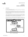
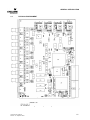
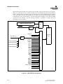
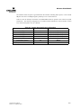
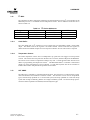
COMPACT PCI-816 USER’S MANUAL The information in this document has been carefully checked and is believed to be entirely reliable. However, no responsibility is assumed for inaccuracies. Furthermore, Cyclone Microsystems, Inc. reserves the right to make changes to any products herein to improve reliability, function, or design. Cyclone Microsystems, Inc. neither assumes any liability arising out of the application or use of any product or circuit described herein, nor does it convey any license under its right or the rights of others. Revision 1.0, September 2002 Cyclone P/N 800-0816 Copyright 2002 by Cyclone Microsystems, Inc. CONTENTS CHAPTER 1 GENERAL INTRODUCTION 1.1 INTRODUCTION.............................................................................................................................. 1-1 1.2 FEATURES ...................................................................................................................................... 1-2 1.3 OVERVIEW ...................................................................................................................................... 1-3 1.4 SPECIFICATIONS............................................................................................................................ 1-3 1.5 ENVIRONMENTAL...........................................................................................................................1-3 1.6 PHYSICAL ENVIRONMENT ............................................................................................................ 1-5 1.7 REFERENCE MANUALS .................................................................................................................1-6 CHAPTER 2 MPC8260 PROCESSOR 2.1 MPC8260 PROCESSOR.................................................................................................................. 2-1 2.2 BYTE ORDERING............................................................................................................................ 2-1 2.3 SYSTEM RESET.............................................................................................................................. 2-1 2.4 POWERPC MPC603E CORE CACHE, BUFFERS, ARRAYS......................................................... 2-2 2.5 MEMORY MAP................................................................................................................................. 2-2 2.6 INTERRUPTS (EXCEPTIONS)........................................................................................................ 2-3 2.7 MPC8260 INTERRUPT PROCESSING........................................................................................... 2-3 CHAPTER 3 HARDWARE 3.1 SDRAM............................................................................................................................................. 3-1 3.2 FLASH ROM.....................................................................................................................................3-1 3.3 NON-VOLATILE PARAMETER MEMORY....................................................................................... 3-1 3.4 CONSOLE SERIAL PORT ............................................................................................................... 3-2 3.5 COUNTER/TIMERS ......................................................................................................................... 3-2 3.6 LEDS ................................................................................................................................................ 3-2 3.7 PCI INTERFACE .............................................................................................................................. 3-4 3.7.1 Primary PCI Arbitration........................................................................................................ 3-4 3.7.2 Secondary (60x) Bus and Arbitration...................................................................................3-4 3.7.3 DMA Channels .................................................................................................................... 3-4 3.8 I2O MESSAGE UNIT........................................................................................................................3-4 3.9 JTAG/COP SUPPORT.....................................................................................................................3-5 3.10 GEOGRAPHIC ADDRESSING ........................................................................................................ 3-5 3.11 TDM E1 PORTS...............................................................................................................................3-6 3.11.1 PM4351 COMET .................................................................................................................3-6 3.11.2 TDM E1 Port LEDs..............................................................................................................3-6 3.11.3 TDM E1 Port Connectors ....................................................................................................3-6 3.12 I2C BUS............................................................................................................................................3-7 3.12.1 Clock Buffer ......................................................................................................................... 3-7 3.12.2 Temperature Sensors.......................................................................................................... 3-7 3.13 HOT SWAP ...................................................................................................................................... 3-7 3.13.1 Hot Swap Extraction Process .............................................................................................. 3-8 CPCI-816 User’s Manual Revision 1.0, September 2002 i CONTENTS 3.13.2 Hot Swap Insertion Process ................................................................................................3-8 3.14 SOFTWARE RESET ........................................................................................................................3-8 3.15 CLOCKING....................................................................................................................................... 3-9 ii CPCI-816 User’s Manual Revision 1.0, September 2002 CONTENTS LIST OF FIGURES Figure 1-1. PCI-816 Block Diagram .......................................................................................................1-1 Figure 1-2. Physical Configuration......................................................................................................... 1-5 Figure 2-1. MPC8260 Interrupt Routing................................................................................................. 2-4 Figure 3-1. Board Status LED Register, F820 0000H............................................................................3-3 Figure 3-2. Port Status LED Register Bitmap, PA<31:24>.................................................................... 3-3 Figure 3-3. Geographic Addressing Register, F820 0000H...................................................................3-5 Figure 3-4. Hot Swap Register,F800 0000h .......................................................................................... 3-8 CPCI-816 User’s Manual Revision 1.0, September 2002 iii CONTENTS LIST OF TABLES Table Table Table Table Table Table Table Table Table iv 1-1. 1-2. 2-1. 2-2. 2-3. 3-1. 3-2. 3-3. 3-4. CPCI-816 Power Requirements .......................................................................................... 1-3 Environmental Specifications .............................................................................................. 1-4 HRCW Address Map ........................................................................................................... 2-1 PowerPC Exception Summary............................................................................................ 2-3 System Interrupt Vector Configuration ................................................................................ 2-5 SDRAM Performance..................................................................................................... 3-1 Console Port Connector ...................................................................................................... 3-2 JTAG/COP PIN ASSIGNMENT........................................................................................... 3-5 I2C Device Addresses ........................................................................................................ 3-7 CPCI-816 User’s Manual Revision 1.0, September 2002 GENERAL INTRODUCTION CHAPTER 1 GENERAL INTRODUCTION 1.1 INTRODUCTION The CPCI-816 is a high-performance CompactPCI peripheral board featuring four E1 communication ports. A block diagram is shown in Figure 1-1. The board is based on the MPC8260 PowerQUICC II communications processor. The MPC8260 integrates a variant of the PowerPC MPC603e TM RISC microprocessor, an SIU (system interface unit, a flexible memory and peripheral controller) and a CPM (communications processor module, a controller that supports many communication protocols, including ATM, Ethernet and in this application, time division multiplexed channels). A Galileo Technology GT-64130 System controller for PowerPC Processors bridges the CompactCPI bus to the local processors 60x bus. The GT-64130 also provides the memory controller for 64Mbytes of on board SDRAM. The SIU of the MPC8260 controls the 2MB FlashROM. The CPM of the MPC8260 also provides the console serial port, the I2 C port and generic I/O control. The four E1 ports have a 75 ohm line interface and BNC connectors for connection to coax cable.Software development tools for PowerPC processors are available from a variety of vendors, and a Board Support Package (BSP) for the pSOSystem real time operating system is available from Cyclone. E1 Port E1 Port E1 Port E1 Port Serial Port (Console) I2 C 2 MB Flash ROM Power QUICC II Processor (MPC 8260) Power PC (60x) bus 66 MHZ/64bit 64MB SDRAM (8Mx64) Memory Bus 66 MHZ/64bit PCI-to-Power PC Bridge (Galileo GT-64130) Primary Compact PCI Bus 33 MHZ/64bit Figure 1-1. PCI-816 Block Diagram CPCI-816 User’s Manual Revision 1.0, September 2002 1-1 GENERAL INTRODUCTION 1.2 1-2 • FEATURES MPC8260 Processor • GT-64130 System Controller • SDRAM • CompactPCI™ Interface • Flash ROM 2 Mbytes of in-circuit sector-programmable Flash ROM. • Console Serial Port An RS-232 serial port is provided for a console terminal or workstation connection. The serial port supports up to 115 Kbps and uses a phone jack to DB25 cable supplied with the CPCI-816 board. • E1 Communication Ports Four E1 ports, each based on the PMC-Sierra PM-4351 Combined T1/E1 Framer/Transceiver (COMET). The COMET integrates a T1/E1 longhaul or shorthaul line interface circuit with a software selectable T1/E1 framer. • Hot Swap The CPCI-816 is a Full Hot Swap board, compliant with PICMG 2.1. • Timers • Non-Volatile RAM Non-volatile storage is provided by Flash ROM on the CPCI-816. One 64 Kbyte sector of the Flash ROM is reserved for the storage of non-volatile boot and system parameters. • DMA Controller The GT-64130 provides four separate DMA channels for high throughput data transfers between PCI bus agents and the local SDRAM memory. • I2 O Messaging The CPCI-816 supports the I2O specification for inter processor communication. The microprocessor is Motorola’s integrated MPC8260 PowerPC. The device integrates a Motorola 32-bit PowerPC 603e core, running at 200 MHz internally, a System Interface Unit (SIU) for memory and peripheral control and a Communications Processor Module (CPM), a separate 32-bit RISC controller residing on its own internal bus to process a variety of communications protocols. The core boasts a 16 Kbyte instruction cache and a 16 Kbyte data cache. The GT-64130 functions as a PCI-to-PowerPC bridge with a 64-bit data PCI (primary) bus interface and a 64-bit data 60x bus (secondary) interface. The GT-64130 also has an SDRAM memory controller. Using the SDRAM controller on the bridge allows access to the memory from both the processor and CompactCPI bus. 64 MBytes of 66MHz on board SDRAM. The CPCI-816 meets the PICMG Rev. 2.0 Specification for peripheral adapters. The PCI bus runs at 33MHz. A 32-bit time counter (TMCNT) and a 16-bit periodic interrupt timer (PIT) are available in the processors’ SIU to generate interrupts. CPCI-816 User’s Manual Revision 1.0, September 2002 GENERAL INTRODUCTION 1.3 OVERVIEW The CPCI-816 is a 6U CompactPCI peripheral board with support for four E1 communication ports. The CPCI-816 occupies one slot in a CompactPCI chassis. The CPCI-816 has a 64-bit Primary data bus and a 64-bit Secondary data bus. The Primary bus is the CompactPCI bus. The Secondary bus is a 60x bus that supports the MPC8260. The CPCI-816 uses a Galileo GT-64130 System Controller for PowerPC Processors to bridge between the Primary, CompactPCI bus and the Secondary, local 60x bus. This device complies with the PCI Local Bus Specification, revision 2.1, provides concurrent bus operation, allows buffering for both read and write transactions and provides support for HotSwap operation. The primary PCI interface is 64-bit data but will operate correctly when the CPCI-816 is plugged into a 32-bit CompactPCI slot. The GT-64130 also provides the memory controller for the CPCI-816’s SDRAM. The data path to memory of the CPCI-816 is also 64-bit. The Flash ROM on the CPCI-816 can be reprogrammed by software through a JTAG/COP interface. Utilities to perform this programming are available from software development tool vendors. Additional information on the JTAG/COP interface can be found in section 3.9. Four PMC-Sierra PM4351 Combined T1/E1 Framer/Transceiver (COMET) devices provide the E1 framer and line interface function for the serial data stream (clock, data and sync) provided by the CPM of the MPC8260. The microprocessor interface of each COMET connects to the peripheral controller in the SIU of the MPC8260. The four E1 ports have a 75 ohm line interface and BNC connectors for connection to coax cable. 1.4 SPECIFICATIONS Physical Characteristics The four port CPCI-816 is a single slot, double high CompactPCI peripheral card. Height Depth Width Power Requirements 9.187” (233.35mm) Double Eurocard (6U) 6.299” (160mm) .8” (20.32mm) Four Port version. The CPCI-816 requires +5V, +12V and +3.3V from the CompactPCI backplane J1 connector. Table 1-1. CPCI-816 Power Requirements Voltage Current Typical Current Maximum +3.3V 2.00 Amps 2.80 Amps +5V +12V -12V 1.5 0.13 Amps 0.02 Amps 0.00 Amps 0.18 Amps 0.03 Amps 0.00 Amps ENVIRONMENTAL The CPCI-816 should be operated in a CompactPCI card cage with good air flow. The board can be operated at ambient air temperature of 0-55 degrees Celsius, as measured at the board. CPCI-816 User’s Manual Revision 1.0, September 2002 1-3 GENERAL INTRODUCTION Table 1-2. ENVIRONMENTAL SPECIFICATIONS 1-4 Operating Temperatures 0 to 55 Degrees Celsius Relative Humidity (noncondensing) 0-95% Storage Temperatures -55 to 125 Degrees Celsius CPCI-816 User’s Manual Revision 1.0, September 2002 GENERAL INTRODUCTION 1.6 PHYSICAL ENVIRONMENT Figure 1-2. Physical Configuration CPCI-816 User’s Manual Revision 1.0, September 2002 1-5 GENERAL INTRODUCTION Figure 1-2 is a physical diagram of the CPCI-816 Adapter, showing the reference designators of jumpers, connectors, and ICs. Refer to this figure when component locations are referenced in the manual text. 1.7 REFERENCE MANUALS MPC8260 PowerQUICC II User’s Manual Order Number MPC8260UM/D Rev. 0 Motorola Literature Distribution P.O. Box 5405 Denver, CO 80217 (800) 441-2447 PowerPC Microprocessor Family: The Programming Environments for 32-BIT Micro processors, Rev. 1 Order Number MPCFPE32B/AD Motorola Literature Distribution P.O. Box 5405 Denver, CO 80217 (800) 441-2447 GT-64130 Product Review (datasheet) Rev 1.1 Galileo Technology, Inc. 142 Charcot Avenue San Jose, CA 95131 (408) 367-1400 (408) 367-1401 www.galileoT.com PM4351 Datasheet (PMC-970624) PM4351 Programmers Guide (PMC-990615) PMC-Sierra, Inc. Suite 105 8555 Baxter Place Burnaby, BC V5A 4V7 Canada (604) 415-6000 (604) 415-6209 (Fax) http://www.pmc-sierra.com 1-6 ComCompactPCI Specification PCI Industrial Computers Manufacturing Group 301 Edgewater Place, Suite 220 Wakefield, MA 01880 (617) 224-1100 (617) 224-1239 Fax PCI Local BIOS Specification, Revision 2.1 PCI Special Interest Group 2575 NE Kathryn Street #17 Hillsboro, OR 97214 (800) 433-5177 (U.S.) (503) 693-6232 (International) (503) 693-8344 (Fax) I2 O Specification, Revision 1.0 I2 O Special Interest Group (415) 750-8352 http://www.i2osig.org CompactPCI Hot Swap Specification, PICMG 2.1, R1.0 PCI Industrial Computers Manufacturing Group 301 Edgewater Place, Suite 220 Wakefield, MA 01880 (617) 224-1100 (617) 224-1239 Fax CPCI-816 User’s Manual Revision 1.0, September 2002 MPC8240 PROCESSOR CHAPTER 2 MPC8260 PROCESSOR 2.1 MPC8260 PROCESSOR The MPC8260 contains a PowerPC 603e core processor which is configured to run at 200 MHz. This RISC processor utilizes a superscalar architecture that can issue and retire as many as three instructions per clock. The core features independent 16 Kbyte, four-way set-associative, physically addressed caches for instructions and data and on-chip instruction and data memory management units (MMUs). The System Interface Unit, or SIU, includes the 64-bit 60x bus, a 32-bit local bus and a flexible memory and peripheral controller. The 60x bus is connected to the GT-64130 and runs at 66MHz. The local bus is not used on the CPCI-816. The peripheral controller of the SIU is used for access to the Comet registers and the Flash ROM. The memory controller is not used for SDRAM control, instead the GT64130s’ memory controller is used to control SDRAM. The Communications Processor Module, or CPM, is a 32-bit RISC controller within the MPC8260 that supports many communication protocols, including ATM, Ethernet and on the CPCI-816, four time division multiplexed channels. The CPM is configured to run at 133 MHz. 2.2 BYTE ORDERING The CPCI-816 is designed to run in big endian mode. The byte ordering determines how the core accesses local memory and the PCI bus. Big endian stores the most significant byte in the lowest address. 2.3 SYSTEM RESET The 8 bit wide Flash ROM is located in the address range FFE0 0000h through FFFF FFFFh as shown in figure 2.1, the CPCI-816 memory map. The MPC8260 Hard Reset Configuration Word (HRCW) is located at address FFE0 0000h as shown in Table 2-1 Table 2-1. HRCW Address Map HRCW Byte Offset Flash Address 0 FFE0 0000h 1 FFE0 0008h 2 3 FFE0 0010h FFE0 0018h Value 14h A2h 00h 45h The HRCW provides fundamental system configuration for the MPC8260 as described in section 5.4 of the MPC8260 PowerQUICC II User’s Manual. The configuration items addressed by the HRCW include the flash memory address, flash memory data access width, system clock setup, pin multiplexing selections, 60x bus initialization, and location of the internal control registers as determined by the Internal Memory Map Register (IMMR). CPCI-816 User’s Manual Revision 1.0, September 2002 2-1 MPC8260 PROCESSOR After reading the HRCW, the PowerPC core obtains its first instruction from the System Reset Exception Vector, which is located in Flash ROM at address FFF0 0100h. This is the start of the low level board initialization code which completes the MPC8260 configuration, sets up the remaining devices on the CPCI-816, including the Galileo GT-64130 System Controller, and then loads the operating system. 2.4 POWERPC MPC603E CORE CACHE, BUFFERS, ARRAYS The processor core provides independent on-chip, 16-Kbyte, four-way set-associative, physically addressed caches for instructions and data and on-chip instruction and data memory management units (MMUs). The MMUs contain 64-entry, two-way set associative, data and instruction lookaside buffers (TLB) that provide support for demand-paged virtual memory address translation and variable-sized block translation. The processor also supports block address translation (BAT) arrays of four entries each. As an added feature to the MPC603e core, the MPC8260 can lock the contents of one to three ways in the instruction and data cache (or the entire cache). 2.5 MEMORY MAP Figure 2-1 shows the CPCI-816 memory map. FLASH ROM FFE0 0000 LOCAL DEVICES FFE0 0000 F800 0000 OUTBOUND PCI (TO HOST) FF70 0100 F000 0000 FA04 0000 Comet #4 FA03 0000 Comet #3 D000 0000 FA02 0000 OUTBOUND PCI (TO LINK BOARDS) 0000 0000 Comet #2 FA01 0000 Comet #1 FA00 0000 FC02 0000 0400 0000 NON CACHEABLE SDRAM MMR FC00 0000 0200 0000 0000 0000 CACHEABLE SDRAM GT64130 REGS Geographic Address REG (read) Status LED REG (Write) FB00 1000 FB00 0000 F820 1000 F820 0000 F820 0000 Hot Swap REG F800 0000 Figure 1-1. CPCI-816 Memory Map 2-2 CPCI-816 User’s Manual Revision 1.0, September 2002 MPC8240 PROCESSOR 2.6 INTERRUPTS (EXCEPTIONS) The PowerPC architecture defines an exception handling mechanism which is implemented in the MPC8260 603e core and described in Chapter 6 of the PowerPC Microprocessor Family: The Programming Environments for 32-Bit Microprocessors (PEM). They treat external interrupts as one case of possible exceptions to the PowerPC core. The PowerPC architecture allocates a region of memory to store exception handlers. Each exception handler is 256 bytes in size, and there are approximately fourteen recognized exceptions in the PowerPC architecture. For example, the System Reset Exception is assigned to vector offset 100h. The PowerPC Exception Vector region base address is initially set to FFF0 0000h for the CPCI-816, and later moved to 0000 0000h when the program instructions are being executed from SDRAM. Table 2-2 lists the PowerPC exceptions. Table 2-2. PowerPC Exception Summary 2.7 Exception Type Vector Offset System reset 100h Machine check 200h Data storage 300h Instruction storage 400h External interrupt 500h Alignment 600h Program 700h Floating point unavailable 800h Decrementer 900h System call C00h Trace D00h MPC8260 INTERRUPT PROCESSING Within the MPC8260, the System Interface Unit (SIU) performs the interrupt controller functions for external interrupt sources. There are two exceptions to the PowerPC core which are controlled by the SIU, machine check and external interrupt. CPCI-816 User’s Manual Revision 1.0, September 2002 2-3 MPC8260 PROCESSOR The external interrupt exception is presented to the PowerPC core by the SIU when any of approximately sixty interrupts are active. All SIU interrupt sources can be masked and prioritized via software control. When an external interrupt is active, the interrupt service routine (ExISR) located at exception vector offset 500h is executed. The ExISR must then read the SIU Interrupt Vector Register (SIVEC), to determine the source of the interrupt. Once the ExISR reads the SIVEC, it then calls the handler registered for that interrupt. The SIU interrupt controller is described in Chapter 4.2 of the PowerQUICC II User’s Manual. Software Watchdog Timer OR IRQ0 IRQ[0-7] Comet 2(PortC[13]) Comet 3(PortC[14]) Comet 4(PortC[15]) MCP TMCNT PIT / 12 Comet 1(PortC[12]) Fall/ Level Edge/ Fall Timer 1 Timer 2 Timer 3 FCC1 FCC2 FCC3 MCC1 MCC2 SCC1 SCC2 SCC3 SCC4 SMC1 SMC2 SPI I 2C IDMA1 IDMA2 IDMA3 IDMA4 SDMA RISC Timers Power PC Core INT Interrupt Controller Port C[0-11] / 8 Figure 2-1. MPC8260 Interrupt Routing 2-4 CPCI-816 User’s Manual Revision 1.0, September 2002 MPC8240 PROCESSOR The machine check exception is generated when the software watchdog timer expires, or the external IRQ0# is activated. The IRQ0# signal is pulled up to Vcc on the CPCI-816. Table 2-3 lists the interrupt connections to the MPC8260 which are specific to the CPCI-816 system architecture. The interrupt configuration for all other internal CPM devices can be found in section 4.2.4 of the PowerQUICC II User’s Manual. Table 2-3. System Interrupt Vector Configuration System Interrupt Description SIU Interrupt Number Interrupt Source Description Galileo GT-64130 19 IRQ1# COMET 1 45 Parallel I/O Port C, pin 12 COMET 2 46 Parallel I/O Port C, pin 13 COMET 3 47 Parallel I/O Port C, pin 14 COMET 4 Temperature Sensor 1 Temperature Sensor 2 CPCI-816 User’s Manual Revision 1.0, September 2002 48 25 25 Parallel I/O Port C, pin 15 IRQ7# IRQ7 # 2-5 HARDWARE CHAPTER 3 HARDWARE 3.1 SDRAM The CPCI-816 is equipped with 64M bytes of SDRAM mounted on the card. The memory is made up of 4, 128Mbit (8M x 16) devices in an 8M by 64 bit configuration. There is no expansion memory slot, 64M bytes is the only configuration supported. The memory controller of the GT-64130 bridge allows zero data-to-data wait state operation of the SDRAM at 66 MHz, yielding a theoretical maximum throughput of 504 Mbytes per second. The memory controller must support memory accesses from both the processor and the CompactPCI bus. Actual performance of the PCI-816s memory is dependent on the bursting capability of the master and the latencies incurred in accessing the SDRAM. The processor only bursts for four beats or transfers. The PCI bus can, theoretically, burst indefinitely but incurs latencies across the bridge to the SDRAM. Table 3-1 shows some sample performance numbers for read and write accesses to the SDRAM from the CPU and the PCI bus. These examples are estimates and assume there is no bus contention for memory. Table 3-1. 3.2 SDRAM Performance Cycle Type Clocks CPU Single Read (8 bytes) CPU Burst Read (32 bytes) 11 14 Performance Bandwidth 46 Mbytes/sec 144 Mbytes/sec PCI Single Read (8 bytes) PCI Burst Read (256 bytes) CPU Single Write (8 bytes) CPU Burst Write (32 bytes) PCI Single Write (8 bytes) 44 82 3 6 2 11 Mbytes/sec 197 Mbytes/sec 168 Mbytes/sec 336 Mbytes/sec 126 Mbytes/sec PCI Burst Write (256 bytes) 39 207 Mbytes/sec FLASH ROM The CPCI-816 provides 2 Mbytes of sector-programmable Flash ROM for non-volatile code storage. The Flash ROM is located in local memory space at address FFE0 0000h through FFFF FFFFh. The mapping ensures that, after a reset, the MPC8260 processor can load the hard reset configuration word located at FFE0 0000h. 3.3 NON-VOLATILE PARAMETER MEMORY One 64 Kbyte sector of the Flash ROM on the CPCI-816 is reserved for the storage of application parameters. The boot parameter block is divided into 4 Kbyte sections, each of which may be used for the storage of a set of boot parameters. CPCI-816 User’s Manual Revision 1.0, September 2002 3-1 HARDWARE 3.4 CONSOLE SERIAL PORT A single console serial port with an RS-232 line interface has been included on the CPCI-816. The port is connected to a RJ-11 style phone jack on the adapter, and can be connected to a host system using the included phone jack to DB-25 cable (Cyclone P/N 530-2002). The pinout of the console connector is as shown in table 3-2. Table 3-2. Console Port Connector Pin Signal Description 1 Not Used 2 GND Ground 3 TXD Transmit Data 4 RXD Receive Data 5 Not Used 6 Not Used Note: Pin 1 is the contact to the extreme left looking into the console port opening, with the tab notch facing down. The serial port is based on the serial management controller (SMC1) device of the MPC8260 communications processor module. The SMC is placed in UART mode and its clock is derived from one of the internal baud rate generators. The serial port is capable of operating at speeds from 9600 to 115,200 bps, and can be operated in interrupt-driven or polled mode. For a detailed description of the SMC UART mode operation refer to Sec 26.3, “SMC in UART Mode” of the PowerQUICC II User’s Manual. 3.5 COUNTER/TIMERS The MPC8260 CPM is equipped with four 16-bit, or two 32-bit on-chip general purpose counter/timers as described in Chapter 17 of the PowerQUICC II User’s Manual. The timers can be individually programmed to generate interrupts to the processor when they count down to zero. 3.6 LEDS The CPCI-816 has twelve green LEDs and one blue LED. The green LEDs report board and port status and the blue LED reports hot swap status. The green LEDs labeled, IOP, ACT, STAT0, and STAT1 are under software control and are used to indicate board status. The board status LEDs are controlled by a write-only register which is located at address F820 0000H. The Board Status LED Register bitmap is shown in Figure 3-1. Writing a one to a bit location in this register will turn on the corresponding LED. In Figure 3-1, bit 7 is labeled SWRST see section 3.14 for more information. 3-2 CPCI-816 User’s Manual Revision 1.0, September 2002 HARDWARE ACT STAT0 STAT1 IOP SWRST 7 Reserved 6 5 4 3 2 1 0 Write Only 1= LED On 2=LED Off Figure 3-1. Board Status LED Register, F820 0000H The remaining eight green LEDs are associated with the E1 ports and are intended to indicate the line interface status. The line interface LEDs are controlled by a read/writable register located in the upper 8 bits of Port A of the MPC8260s CPM. A given ports’ LNK LED should be ON when that port has established a connection with its link partner. A given ports’ ACT LED should be ON when that port sees transmit or receive activity. These LEDs are controlled by writing to the Parallel I/O Port A Data Register, bits 24 through 31. To turn on an LED, clear the bit associated with the desired LED. To turn off an LED, set the bit associated with the desired LED. Port0 LNK Port0 ACT Port1 LNK Port1 ACT Port2 LNK Port2 ACT Port3 LNK Port3 ACT PA31 PA30 PA29 PA28 PA27 PA26 PA25 PA24 Figure 3-2. Port Status LED Register Bitmap, PA<31:24> The blue LED is used for Hot Swap operations. Refer to section 3.12 for additional information. CPCI-816 User’s Manual Revision 1.0, September 2002 3-3 HARDWARE 3.7 PCI INTERFACE The CPCI-816 uses a Galileo Technologies GT-64130 to bridge the 33MHz/64-bit CompactPCI bus to the 66MHz/64-bit 60X bus of the MPC8260. The GT-64130 is capable of supporting two 32-bit PCI interfaces at 66MHz, but is configured on the CPCI-816 for one 64-bit PCI interface at 33MHz. The GT-64130 can be either a master initiating a PCI bus operation or a target responding to a PCI bus operation. The following PCI bus cycles are supported: Memory Read/Write, Interrupt Acknowledge, Special Cycle, I/O Read/Write and Configuration Read/Write. The GT-64130 incorporates 192-bytes of posted write and read prefetch buffers for efficient data transfer between the PCI bus to memory and CPU/memory to PCI bus. 3.7.1 Primary PCI Arbitration The primary PCI bus arbitration is provided by host of the CompactPCI system. 3.7.2 Secondary (60x) Bus and Arbitration The GT-64130 has a 32-bit multiplexed Address/Data Bus that needs to be demultiplexed into the separate Address and Data busses of the 60x bus. The GT-64130 offers two methods of demultiplexing the A/D bus; QuickSwitch and Glueless. The Glueless method saves components on the board but costs an extra clock cycle at each transaction to avoid bus contention. The QuickSwitch method requires more components, but runs faster without the extra clock cycle. The CPCI-816 uses the Quickswitch method, keep this in mind when reading the GT-64130 data. Since the MPC8260 processor is the only 60x bus master, there is no Secondary (60x) bus arbitration, the MPC8260 always owns the 60x bus. 3.7.3 DMA Channels The GT-64130 has four DMA controllers. On the CPCI-816, data movement occurs between the PCI bus and the memory bus. Each DMA transfer uses one of two internal 64-byte FIFOs for moving data. Both the local processor and PCI masters can initiate a DMA transfer. 3.8 I2 O MESSAGE UNIT The GT-64130 includes hardware support for the Intelligent I/O (I 2O) Standard. This support includes all of the registers required for implementing the I2 O message unit (MU) as defined in the I2 O specification. The GT-64130’s MU can operate with generic messages and doorbell registers to facilitate communications between the host processor and peripheral processors. The intelligent input output (I2 O) specification allows architecture-independent I/O subsystems to communicate with an OS through an abstraction layer. The specification is centered around a messagepassing scheme. An I2 O-compliant peripheral (IOP) is comprised of memory, processor, and input/ output devices. The IOP dedicates a certain space in its local memory to hold inbound (from the remote processor) and outbound (to the remote processor) messages. The space is managed as memorymapped FIFOs with pointers to this memory maintained through the GT-64140 I2O registers. Please refer to the GT64130 User’s Manual for I2O register descriptions, FIFO descriptions and an I2O message queue example. 3-4 CPCI-816 User’s Manual Revision 1.0, September 2002 HARDWARE 3.9 JTAG/COP SUPPORT The MPC8260 contains a joint test action group (JTAG) interface. In addition to boundary scan operations, the JTAG interface is also used to access the common on-chip processor (COP) function of the MPC8260. The COP function of PowerPC processors allows a remote computer system (typically a PC with dedicated hardware and debugging software) to access and control the internal operations of the processor. The 16 pin COP header on the CPCI-816 is located at J5. The COP header is intended for use with WindRiver Systems visionICE emulators. The COP header definition is shown in Table 33. Table 3-3. JTAG/COP PIN ASSIGNMENT Signal Pin Pin Signal TDO 1 2 QACK# TDI 3 4 TRST# QREQ 5 6 +3.3V TCK 7 8 N/C TMS SRESET# COP_RESET# CHKSTOP 3.10 9 11 13 15 10 12 14 16 N/C GND N/C GND GEOGRAPHIC ADDRESSING CompactPCI backplanes that support 64-bit connector pin assignments are required to provide a unique differentiation based upon which physical slot the board has been inserted. The CPCI-816 makes this definition available to the software. The definition for GA[4:0] is shown in Figure 3-3. GA0 GA1 GA2 GA3 GA4 7 Reserved 6 5 4 3 2 1 0 Read Only 1= +5v 0= GND Figure 3-3. Geographic Addressing Register, F820 0000H. CPCI-816 User’s Manual Revision 1.0, September 2002 3-5 HARDWARE 3.11 TDM E1 PORTS The four TDM E1 ports are based on the PMC-Sierra PM4351 Combined E1/T1 Transceiver/Framer (COMET). Internal analog circuitry allows direct reception and transmission of E1 compatible signals. The CPCI-816 adds the required external circuitry (transformer, line protection and line termination) to complete the E1 port. In the receive direction, the COMET recovers clock and data from the E1 signal and presents it to the CPM of the MPC8260 as three signals; clock, sync and data. In the transmit direction, the COMET takes the “three wire” (sync, clock and data) signals from the MPC8260 and converts it to a an E1 signal. 3.11.1 PM4351 COMET A PMC-Sierra COMET device (PM4351) provides the framer and line interface functions for each E1 port of the CPCI-816. The COMET is a feature-rich, software configurable device, allowing feature selection without changes to external circuitry. This section will explain how the COMET has been configured on the CPCI-816, see the COMET data sheet and programmers guide for a complete description of the device itself. The receive TIP and RING and the transmit TIP and RING signals connect to line termination resistors, an isolation transformer, line protection circuitry, EMI filters and BNC connectors to complete the line interface of each E1 port. The digital line interface pins are not used; the RDAT and RCLKI pins are grounded, the TDAT and TFP pins are not connected. The microprocessor (register) interface of each COMET is memory mapped to the locations indicated in Figure 1.1, CPCI-816 Memory Map. The TCLKI pin and the XCLK pin of each COMET is attached to a free-running 2.048MHz crystal clock oscillator, the TCLKO pin is not connected. The “Backplane Transmit Interface” and the “Backplane Receive Interface” of the COMET are used to connect to the MPC8260. The clock, frame pulse and data pins (BTCLK, BTFP, BTPCM, BRCLK, BRFP, BRPCM) from the backplane interface are used, the signaling pins (BTSIG and BRSIG) are not used. The BTSIG pin (an unused input pin) is pulled down. 3.11.2 TDM E1 Port LEDs The COMET device does not provide any LED outputs that would indicate E1 port or line status. Instead, the ACT and LNK LEDs at each port of the CPCI-816 are under software control. See section 3.6, LEDs for operation of the Port Status LEDs. 3.11.3 TDM E1 Port Connectors Each TDM E1 port uses two 75 ohm BNC connectors, one for transmit and one for receive. These connectors are electrically isolated from the front panel (the shield of the connector is not connected to chassis ground). The shield of the connector is RING and the center conductor is TIP. Cabling to the CPCI-816 should be with 75 ohm coaxial cable such as RG59B/U. 3-6 CPCI-816 User’s Manual Revision 1.0, September 2002 HARDWARE 3.12 I2 C BUS The CPCI-816 has three components attached to the Inter-Integrated Circuit (I 2C) bus interface of the MPC8260 processor: a clock buffer and two temperature sensors. The I 2C addresses of the devices are shown in Table 3-4. Designator U16 U8 U7 3.12.1 Table 3-4. I2 C Device Addresses Device Function CDC319 Clock Buffer LM75 Temperature Sensor 0 LM75 Temperature Sensor 1 Address 1101001x 1001000x 1001001x Clock Buffer The clock buffer has an I2C interface to access registers that can individually enable a clock buffer output. The default value of the registers is all clocks enabled. Breeze code alters the registers to disable unused clock buffer outputs for noise and power reduction. No user intervention is required. 3.12.2 Temperature Sensors The LM75 temperature sensors have overtemperature trip points that will trigger an interrupt when crossed. The sensors have been placed on the board at U7 and U8, and share IRQ7# at the MPC8260. The sensors can be read for a temperature reading at any time. Consult the LM75 data sheet for more details on programming the temperature sensors. The MPC8260 CPM I2 C Controller is described in chapter 34 of the PowerQUICC II User’s Manual. Cyclone Microsystems has drivers available to initialize this interface and perform all operations for the LM75. 3.13 HOT SWAP The CPCI-816 is a PICMG 2.1 compliant Hot Swap board. The CPCI-816 is a “Full Hot Swap” board, with both Hardware and Software Connection control. The CPCI-816 can be used on all platform types; Non-Hot Swap platform for a conventional system, Hot Swap platform for a Full Hot Swap system and on High Availability platform for a High Availability system. See the Hot Swap specification for further explanation of Platform, Board and System types. CPCI-816 User’s Manual Revision 1.0, September 2002 3-7 HARDWARE The Hot Swap specification requires four control and status bits (EIM, LOO, INS, EXT) these are located in the Hot Swap Register at location F800 0000h as shown in Figure 3-4. For further definitions of these bits, refer to the Hot Swap Specification. EIM (1) Mask ENUM# Interrupt (0) ENUM# Interrupt LOO (1) Blue LED ON (0) Blue LED OFF EXT READ (1) ENUM# Asserted (0) Not Asserted WRITE (1) Clear EXT (0) No Action INS READ (1) ENUM# Asserted (0) Not Asserted WRITE (1) Clear INS (0) No Action 7 6 5 4 3 2 1 0 Figure 3-4. Hot Swap Register,F800 0000h 3.13.1 Hot Swap Extraction Process Removal of the CPCI-816 in a Full Hot Swap or High Availability system is the same. The operator first only opens the ejector handles of the board. A switch on the CPCI-816 signals to the system that it is to be extracted. In response, the system will illuminate the Blue Hot Swap LED when extraction is permitted. 3.13.2 Hot Swap Insertion Process Insertion of the CPCI-816 is the same in any Hot Swap system. The operator merely slides the CPCI816 into the desired slot and latches the handles. 3.14 SOFTWARE RESET The CPCI-816 has a feature that allows the board to be reset via software. By writing a logic 1 to bit 7 of the Board Status LED Register (F820 0000h), the CPCI-816 will reset the MPC8260, the GT-64130 and the four COMET devices. Bit 7 of the register will self-clear. 3-8 CPCI-816 User’s Manual Revision 1.0, September 2002 HARDWARE 3.15 CLOCKING The CPCI-816 has three independent clocking domains; Primary PCI Bus, Secondary 60x Bus (& Memory) and Line Interface. The Primary PCI Bus clock is 33MHz and is provided by the CompactPCI bus host. This signal drives the two PCI clock pins of the GT-64130. (There are two clock pins because the GT-64130 is configurable as one 64-bit interface or two 32-bit interfaces and both clock pins must have a valid clock in 64bit mode). The Secondary 60x Bus clock source is an on-board 66MHz free running oscillator. The oscillator output is buffered into seven, synchronous clock signals. To ensure synchronization and signal integrity, each clock signal is dedicated to a device; The Secondary 60x bus side of the GT-64130, the MPC8260, a glue logic CPLD and the four SDRAM chips. The MODCLK[1-3] pins at the MPC8260 and the Hard Reset Configuration Word configure the MPC8260 for a core frequency of 200MHz and a CPM frequency of 133MHz (this is the current maximum available speeds for MPC8260). The Line Interface clock source is an on-board 2.048MHz free running oscillator. The oscillator output is buffered into eight, synchronous clock signals. To ensure signal integrity, each clock signal is dedicated to a device pin; Each of the four Comet devices TCLKI and XCLK pins gets its own clock. CPCI-816 User’s Manual Revision 1.0, September 2002 3-9