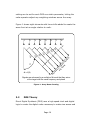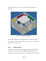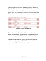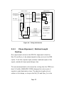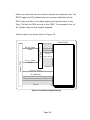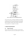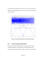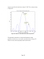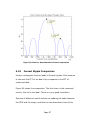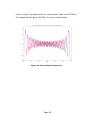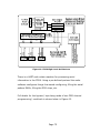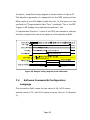
1
Development of an Eight Channel Waveform Generator for Beam-forming Applications By John Ledford Submitted to the graduate degree program in Electrical Engineering and the Graduate Faculty of the University of Kansas, in partial fulfillment of the requirements for the degree of Master of Science in Electrical Engineering. ____________________ Chris Allen - Chair Person Committee Members ____________________ Carl Leuschen ____________________ Sarah Seguin Date Defended: ____________________ The Thesis Committee for John Ledford certifies that this is the approved Version of the following thesis: Development of an Eight Channel Waveform Generator for Beam-forming Applications Committee: ____________________ Chris Allen - Chair Person ____________________ Carl Leuschen ____________________ Sarah Seguin Date Approved: Page 2 ____________________ Acknowledgements I wish to acknowledge my wife for encouraging me when I wanted to be encouraged, kicking me in the pants when I needed to be kicked, and leaving me alone at the appropriate times. You know me better than I do myself. To my children for jumping on my head and not letting me work. You are far more important than work or school. Thanks for helping remind me by endlessly dragging me away to play. To Dr. Chris Allen, whose classes inspired me. Radar was a field I never thought I would be interested in, but your teachings were fascinating and inspiring, and it’s your fault I sought to work with you further. To Dr. Carl Leuschen for helping me figure it out. It has been quite a pleasure working with you on this design, even when you want things I don’t agree with or more to the point want to do. To Dr. Sarah Seguin for the promise of a good working future, and someone else to help with the EMI gospel. To Dr. Prasad Gogineni for the years of work that led to this center and it’s great mission. Also for letting me design this project as part of the UAV radar. Page 3 Abstract An eight-channel direct-digital waveform synthesizer has been developed to enable digital beam steering of the transmitted waveform. Built around the Analog Devices AD9910 DDS chip, this eight-channel waveform generator, when used with an eight element linear antenna array, enables the illuminating radiation pattern to be digitally modified on a pulse-to-pulse basis if desired. Developed in support of airborne radar depth-sounding of the polar ice sheets and outlet glaciers, two key benefits of this capability provides include improved surface clutter suppression and more efficient off-nadir illumination for side-looking imaging of the icebed interface. Adjusting the starting frequency and phase of the waveform produced by each DDS is analogous to introducing an incremental time delay between otherwise identical chirp waveforms, thus providing the required beam-steering control. Additionally, the AD9910, with a 1-GHz maximum clock frequency, provides amplitude control, both intra-waveform and inter-waveform, for time-sidelobe management and radiation-sidelobe management. An FPGA is used for the management of up to 16 waveforms, zeropi phase modulation on a per waveform basis, system communication over a serial port, and loading the DDS configuration settings on each system trigger. The board provides matched clock and sync inputs in order to guarantee phase alignment across the multiple DDS chips. Page 4 Table of Contents 1 Introduction ................................................................... 11 2 Theory ........................................................................... 13 3 2.1 Beam-forming ........................................................... 13 2.2 DDS Theory .............................................................. 14 Implementation .............................................................. 17 3.1 System Specifics........................................................ 17 3.1.1 Packaging............................................................ 17 3.1.2 System Clock....................................................... 18 3.1.3 Timing Requirements ............................................ 19 3.1.4 Waveforms UAV Style ........................................... 19 3.1.5 Play-List UAV Style ............................................... 20 3.1.6 Location in UAV Radar System ............................... 21 3.2 Board Realized .......................................................... 22 3.2.1 Board Level Block Diagram .................................... 23 3.2.2 PCB Parameters ................................................... 24 3.2.3 Signal Integrity .................................................... 26 3.2.4 Power Sequencing Requirements ............................ 28 3.3 Parameters / Specs .................................................... 28 3.4 DDS Information........................................................ 30 3.4.1 Chip Selection ...................................................... 30 3.4.2 Ramp Generation ................................................. 31 3.4.3 Amplitude Shaping ............................................... 32 3.4.4 Output Level ........................................................ 32 3.5 Timing Considerations ................................................ 33 3.5.1 Clock / Sync Distribution Requirements ................... 33 3.5.2 Phase Alignment / Matched Length Routing .............. 35 Page 5 3.5.3 4 Timing Buffer Issue .............................................. 37 Experimental Results ....................................................... 38 4.1 Signal Integrity.......................................................... 38 4.2 Ref_Clk and Sync_In Alignment ................................... 43 4.3 Amplitude Shaping ..................................................... 46 4.4 Amplitude Settings..................................................... 49 4.5 Chirp Results – Scope................................................. 49 4.6 Chirp Results – Spectrum Analyzer ............................... 50 4.7 Single Frequency Output ............................................. 53 4.8 Chirp Results – Data Collection and Processing............... 54 4.9 Pulse Compressed Results ........................................... 55 4.10 Fresnel Ripple Comparison .......................................... 57 4.11 Beam-forming Results ................................................ 59 4.12 Per-Waveform Loading Time........................................ 64 5 Conclusions and Future Work ............................................ 66 5.1 Conclusions............................................................... 66 5.2 Lessons learned ......................................................... 66 5.3 Future Work .............................................................. 69 6 References ..................................................................... 69 7 Appendix A: User Manual.................................................. 70 7.1 Overview .................................................................. 70 7.2 Board Architecture ..................................................... 72 7.3 FPGA Architecture ...................................................... 74 7.4 Software Command & Configuration Language ............... 80 7.4.1 Serial Port Setup .................................................. 81 7.4.2 Stream Writes vs. Individual Byte Read/Writes ......... 81 7.4.3 Packet Format...................................................... 82 7.4.4 Reading / Writing Individual Registers ..................... 82 Page 6 7.4.5 7.5 Stream Writes...................................................... 83 Configuration ............................................................ 83 7.5.1 Load Preference File into Control Database............... 83 7.5.2 Waveform Generator Configuration ......................... 84 7.5.3 Internal Timing Generator Configuration .................. 84 7.5.4 Resetting the DDS chips ........................................ 85 7.5.5 Writing Static Registers in the DDS Chips................. 85 7.5.6 Stream Loading the Dual Port Patterns RAM ............. 88 7.5.7 Go!..................................................................... 89 7.6 External Device Support ............................................. 89 7.7 Appendix A: Memory Map ........................................... 90 7.7.1 Summary Table.................................................... 90 7.7.2 0x31 – Scratch / Reflection Register........................ 91 7.7.3 0x32 – FPGA Revision Major / Middle ...................... 91 7.7.4 0x33 – FPGA Revision Minor................................... 91 7.7.5 0x34 – Wavegen Configuration............................... 91 7.7.6 0x35 – Internal PRF Generator Setting - Upper ......... 92 7.7.7 0x36 – Internal PRF Generator Setting - Middle ........ 92 7.7.8 0x37 – Internal PRF Generator Setting - Lower ......... 93 7.7.9 0x38 – Internal EPRI Generator Setting - Upper........ 93 7.7.10 0x39 – Internal EPRI Generator Setting - Lower........ 93 7.7.11 0x3A – IO Update Time - Upper.............................. 94 7.7.12 0x3B – IO Update Time - Lower.............................. 94 7.7.13 0x3C – Temp Sensor Reading - Upper ..................... 94 7.7.14 0x3D – Temp Sensor Reading - Lower ..................... 95 7.7.15 0x3E – Force Single IO Update Trigger .................... 95 7.7.16 0x40 – DDS Configuration ..................................... 95 7.7.17 0x41 – DDS CS_N Values ...................................... 97 Page 7 7.7.18 0x43 – DDS Byte Send.......................................... 97 7.7.19 0x4B – Reset Serial Pattern RAM Address Counter .... 98 7.7.20 0x4C – Write Byte Serial Pattern RAM ..................... 98 7.7.21 0x50-0x93 Waveform Configuration Values .............. 98 8 Appendix B: Software Operating Routines ......................... 101 8.1 8.1.1 Higher Level Routines ......................................... 101 8.1.2 Base Routines .................................................... 102 8.2 9 serialDriver.c........................................................... 101 dds_8ch.c ............................................................... 102 8.2.1 int setTimeGenParam() ....................................... 103 8.2.2 int timeGenCtrlUpdate() ...................................... 103 8.2.3 int configWfs() ................................................... 103 8.2.4 int initDDS() ...................................................... 104 Appendix C: FPGA Code ................................................. 106 9.1 accessory_stuff.v ..................................................... 106 9.2 dds_8ch_wfg.ucf...................................................... 106 9.3 dds_8ch_wfg.v ........................................................ 106 9.4 dds_controller.v....................................................... 107 9.5 debug_leds.v........................................................... 107 9.6 int_timing_generator.v ............................................. 108 9.7 serial_section.v ....................................................... 108 9.8 state_processing.v ................................................... 108 9.9 uart.v..................................................................... 109 10 Appendix D: Schematics................................................. 110 Page 8 Table of Figures Figure 1: Array Beam-forming ................................................ 14 Figure 2: Basic DDS .............................................................. 15 Figure 3: Digital Ramp in a DDS.............................................. 16 Figure 4: UAV Radar Solid Model ............................................. 18 Figure 5: Example of a Simplified UAV Waveform Database ........ 20 Figure 6: UAV Radar Play List Play Order.................................. 21 Figure 7: A High Level Block Diagram for the UAV Radar ............ 22 Figure 8: Photograph of Final Board......................................... 23 Figure 9: Board Level Block Diagram ....................................... 24 Figure 10: 8 Layer Board Stack-up .......................................... 25 Figure 11: High Speed Signal Transmission and Termination ....... 27 Figure 12: AD9910 Functional Block Diagram (from AD9910 Datasheet)........................................................................... 31 Figure 13: AD9910 Detailed Block Diagram (from AD9910 datasheet) ........................................................................... 33 Figure 14: Timing Architecture............................................... 35 Figure 15: Matched Length Routing ......................................... 36 Figure 16: AD9910 Sync Input (from AD9910 Datasheet) ........... 38 Figure 17: Signal Integrity Test Setup...................................... 40 Figure 18: Ref_Clk Input Signal Integrity Results....................... 41 Figure 19: Sync_In Input Signal Integrity Results...................... 41 Figure 20: Sync_Clk Input to FPGA Signal Integrity Results ........ 42 Figure 21: Repeater Input Signal Integrity Results..................... 43 Figure 22: Ref_Clk Alignment Results ...................................... 45 Figure 23: Sync_In Alignment Results...................................... 46 Figure 24: DDS Outputs without Amplitude Shaping .................. 48 Page 9 Figure 25: DDS Outputs with Amplitude Shaping ....................... 48 Figure 26: Chirp Measured By Scope ....................................... 50 Figure 27: DDS Output Direct Into Spectrum Analyzer, Wide Spectrum............................................................................. 51 Figure 28: DDS Output Direct Into Spectrum Analyzer, Zoomed In .......................................................................................... 52 Figure 29: DDS Output Into Spectrum Analyzer Through SAW Filter, Zoomed In ........................................................................... 53 Figure 30: Single Frequency Output Spectrum .......................... 54 Figure 31: Chirp Results Measured with UAV Radar DAQ............. 55 Figure 32: Ideal vs. Ideal Waveform Pulse Compression ............. 56 Figure 33: Ideal vs. Data Waveform Pulse Compression ............. 57 Figure 34: Fresnel Ripple Comparison ...................................... 58 Figure 35: 195 MHz Nadir Beam, No Window ............................ 60 Figure 36: 195 MHz Nadir Beam, Hanning Window .................... 61 Figure 37: 195 MHz 10 Degree Beam, No Window ..................... 62 Figure 38: 195 MHz 10 Degree Beam, Hanning Window ............. 63 Figure 39: Serial Pattern Load Time......................................... 65 Figure 40: Board Architecture ................................................. 73 Figure 41: FPGA High-Level Architecture .................................. 75 Figure 42: Byte-banged Bypass Logic Block Diagram ................. 76 Figure 43: Block Logic of Regular Playback Mode ....................... 77 Figure 44: Details of RAM Feeding Serial Lines .......................... 79 Figure 45: Sample Timing Diagram from UAV Radar .................. 80 Page 10 1 Introduction Ice sheets are melting and the seas are rising [1]. Rising seas affect the people in low lying areas. Regardless of whether this is manmade or a normal part of the earth’s cycle, humans need to predict the sea level rise, and the impacts of climate changes on the earth. We need to understand how the ice interacts with the bed, how much ice there is, and how it moves across the underlying ground. Scientists are working on the answers to these questions, but lack the data necessary to have the best models possible. The Center for the Remote Sensing of Ice Sheets (CReSIS) was founded with the mission of making the ice measurements, and providing the scientists these data which are necessary to help answer these questions. Modern ice-sounding radars have pushed the technology envelope. What was impossible years ago is now done routinely. These radars are ultra sensitive, high performance instruments, but the measuring of ice in high clutter areas is a very demanding task. Part of the answer is to use multiple beams that allow for illuminating only the area of interest in side looking radar and will reduce clutter effects. To make radar illumination beams you need antennas, and radiated RF energy in special patterns. There are many ways to do this, but the simplest is to use a multi-channel waveform generator. By using one waveform generator channel per antenna element, you Page 11 can digitally program in the special patterns needed to steer the beams in the directions desired. This thesis is about an eight channel waveform generator. At the heart of each generator channel is an Analog Devices AD9910 Direct Digital Synthesis (DDS) chip. All eight channels are synchronous with outputs that can be programmed to provide the beam-forming necessary for the Un-crewed Aerial Vehicle (UAV) radar. There are also plans to use this board in many of CReSIS’ future research work. Page 12 2 Theory To meet the waveform generation needs of the UAV radar, we take a chip from Analog Devices, and wrap all of the timing support and communications needed to support these chips. By using eight of these waveform generating chips, we can have the independently programmed signals that when fed into the RF circuitry and antennas form beams that illuminate in the desired direction. 2.1 Beam-forming Beam-forming is the process of using multiple transmit elements to illuminate some specific target or direction with electromagnetic energy. By using multiple elements and controlling the amplitude and phase of each element, constructive and destructive interference add up such that the remaining RF energy “beam” is pointing in the desired direction. To create the different signals, a time-shift (Δt) is added to each element to delay the signals by fixed amounts. This time-shift delays the signals in time, and thus when it is launched out of the antenna it creates the desired RF energy pattern in the air. In this board, all chips are triggered at the same time. Each waveform generator has it’s own start frequency and start phase setting, so doing beam-forming is a matter of correctly setting the start frequency and phase setting in each DDS chip. These settings can be updated on a per waveform basis, so each waveform can produce a different radiation pattern. Additionally, an amplitude Page 13 setting can be set for each DDS as a static parameter, letting the radar operator adjust any weighting windows across the array. Figure 1 shows eight elements with time-shifts added to create the wave-front at an angle relative to nadir. 1 2 3 4 5 6 7 8 “0” Θ ef ro nt o an f E d qu Ph a as l Fr e e qu en cy Δt t 2Δ t 3Δ t 4Δ t 5Δ t 6Δ t 7Δ W av Δt = f(Θ) Signals are advanced by a multiple of Δt such that they arrive at the target with the same frequency and phase Figure 1: Array Beam-forming 2.2 DDS Theory Direct Digital Synthesis (DDS) uses a high speed clock and digital logic to create the digital codes necessary to make sine waves and Page 14 feeds them to an appropriate D/A converter. The most basic DDS is shown below in Figure 2. Figure 2: Basic DDS Frequency Tuning Word (FTW) is the place you program your desired output frequency. This setting dictates how fast you step through the lookup tables, by means of adding the current phase, to the tuning word to determine what the next phase is. This is done with a digital adder, and a phase accumulator (basically a latch). The output of the phase accumulator is then passed through a sinewave look up table that converts phase to a specific output value. The output of this feeds a D/A which translates the signal into the analog domain. If you want a simple frequency, then the FTW is the only setting you need. However, in radar applications we desire a chirp. Basically we need to ramp the frequency tuning word. We need a start word (FTWstart), a stop word (FTWstop), how often we update Page 15 the word (ramp rate), how big an update step we want (step size), and what we desire the starting phase to be. By using a digital ramp generator, we can feed all of these signals into it, and it will output the frequency tuning word in the desired ramp. The output frequency tuning word vs. time is shown below in Figure 3. Frequency Tuning Word FTWstop Ramp Rate Step Size FTWstart Update Period Trigger Time Figure 3: Digital Ramp in a DDS In a radar application, you set the update period to be at the smallest value possible to get the smoothest transitions, and then set the step size so you reach FTWstop at the desired chirp time (e.g. 10 us). Page 16 The phase accumulator is always reset to the same value, the Phase Offset Word (POW) setting, when the trigger is applied. This allows us to have coherent outputs, and a programmed starting phase (required for zero/pi and beam-steering). 3 Implementation This waveform generator was designed specifically for the UAV radar and has the flexibility to be used for other applications. We will focus here on the UAV specific requirements. To design the UAV radar waveform generator, information about the system is given in section 3.1. There is a discussion of how the board was actually implemented in section 3.2. A complete parameter list is given in section 3.3. Information on the DDS chips selected is in section 3.4. A discussion on timing and synchronization is given in section 3.5 All numbers given are typical. When the radar is used over a range of settings, those ranges and settings are given. It is beyond the scope of this document to re-create all possible settings or future expansion modes. 3.1 3.1.1 System Specifics Packaging The waveform generator was designed to be part of an integrated radar system as shown by the solid model that was used to design Page 17 everything at once in Figure 4. The red board is the waveform generator. Figure 4: UAV Radar Solid Model The waveform generator was designed to be as small as possible, mount inside the UAV radar package, and to mount on a simple flat plate for other future uses. 3.1.2 System Clock The clock in the UAV radar is derived by dividing a 667 MHz SAW oscillator by 6, which gives a 111.1 6 MHz clock frequency. The frequency on this clock is so close to 111 MHz that we say 111 MHz Page 18 and use 9 ns for the period. Any time-based requirements should use the actual number. 3.1.3 Timing Requirements This waveform generator has to live within the confines of radars, and thus has very tight timing requirements, both in the reload speed and the frequency of triggering. The UAV Radar operates with a Pulse Repetition Frequency (PRF), or how often the radar makes a measurement, of up to 12.5 kHz. This sets a cycle period (PRI) minimum of 80 μs. When the PRF trigger occurs but before the waveform trigger, the FPGA has to program all of the waveform specific parameters into the chip. It takes about 10.4 μs to load all of the information into the DDS chips. See Appendix A: User Manual for more information on programming and reprogramming. Therefore the minimum waveform trigger is 10.4 μs after the PRF trigger. 3.1.4 Waveforms UAV Style This waveform generator supports 16 waveforms. It supports a programmable number of presums per waveform. Zero/Pi is supported on a per waveform basis. A simplified example of a UAV Waveform Database is shown in Figure 5. Page 19 WFM # Tx Start Amp Enable Amp Disable 1 2 3 4 5 6 x µs x µs x µs x µs x µs x µs x µs x µs x µs x µs x µs x µs x µs x µs x µs x µs x µs x µs x µs x µs x µs x µs x µs x µs x µs x µs x µs x µs x µs x µs x µs x µs x µs x µs x µs x µs x µs x µs x µs x µs x µs x µs x µs x µs x µs x µs x µs x µs 7 8 9 10 11 12 13 14 15 16 Rx Channel 1 Pad1 Pad2 ... ... Rx Channel 8 Pad1 Pad2 1-1024 1-1024 1-1024 1-1024 1-1024 1-1024 x dB x dB x dB x dB x dB x dB x dB x dB x dB x dB x dB x dB ... ... ... ... ... ... x dB x dB x dB x dB x dB x dB On/Off On/Off On/Off On/Off On/Off 1-1024 1-1024 1-1024 1-1024 1-1024 x dB x dB x dB x dB x dB x dB x dB x dB x dB x dB ... ... ... ... ... On/Off On/Off On/Off On/Off On/Off 1-1024 1-1024 1-1024 1-1024 1-1024 x dB x dB x dB x dB x dB x dB x dB x dB x dB x dB ... ... ... ... ... 0/π # Presums On/Off On/Off On/Off On/Off On/Off On/Off Tx Ch 1 Pad ... ... Tx Ch 8 Pad x dB x dB x dB x dB x dB x dB x dB x dB x dB x dB x dB x dB ... ... ... ... ... ... x dB x dB x dB x dB x dB x dB x dB x dB x dB x dB x dB x dB x dB x dB x dB x dB x dB x dB x dB x dB x dB ... ... ... ... ... x dB x dB x dB x dB x dB x dB x dB x dB x dB x dB x dB x dB x dB x dB x dB x dB x dB x dB x dB x dB ... ... ... ... ... x dB x dB x dB x dB x dB Figure 5: Example of a Simplified UAV Waveform Database 3.1.5 Play-List UAV Style In the UAV radar, we desire to have the ability to set the number of times a given waveform is played. For example, a noise measurement is useful and doesn’t want the averaging effect of presuming. There is also the case that a surface measurement has a high enough return signal that the deep averaging isn’t needed to see the returns. This waveform generator will be downloaded with the number of presums per waveform, trigger delay values, DDS chip settings for each waveform, etc. The play-order for the UAV radar will be waveform 1, then 2, then 3, and will operate in a burst mode, with a presum setting for each Page 20 waveform, and zero/pi enabled on a per-waveform basis. So, for example we desire to run one waveform at nadir (straight down) to gather noise data with one presum (no transmit signal), then eight nadir deep sounding pulses, followed by eight left pointing sounding pulses, followed by eight right pointing sounding pulses. Figure 6 shows a smaller example of one down, four down, four 4 4 4 3 4 3 3 2 3 2 2 1 2 # Presums WF # Direction left, and four right. Figure 6: UAV Radar Play List Play Order 3.1.6 Location in UAV Radar System The waveform generator is part of a much larger radar system. A high level block diagram of the radar system is shown in Figure 7. Page 21 This Board UAV Com T/R Module T/R Module Serial RS-232 Radar CPU PCI Waveform Generator 8 Channel DAQ Analog Conditioning Analog Conditioning T/R Module T/R Module Timing & Control GPS dGPS T/R Module T/R Module Tx Rx Tx T/R Module Rx Tx Rx Tx 8 Rx Rx Tx Rx Tx 8 Tx Rx Tx Rx Tx Rx T/R Module Contains: Power Amp LNA T/R Switch Analog Filtering RF Blanking Loopback Path 3 Temp Sensors 3 Axis Accelerometer T/R Module Figure 7: A High Level Block Diagram for the UAV Radar 3.2 Board Realized A picture of the finished board is shown below in Figure 8. A discussion of how to program the board is attached in Appendix A: User Manual. Radar operating software routines are described in Appendix B: Software Operating Routines. FPGA code is described in. Appendix C: FPGA Code Schematics are described in Appendix D: Schematics. Page 22 Figure 8: Photograph of Final Board 3.2.1 Board Level Block Diagram A simplified block diagram of the board is shown below in Figure 9. The DDS chips have some common control lines, and some that are individual per channel. The board is set up to receive timing signals from the radar timing unit, command and configuration from the radar CPU, and provides some debug and expansion ports. There is a local oscillator for house-keeping functions, and status LEDs. Page 23 DDS1 Sample Clock Control & Timing & Serial EPRI Reset FPGA Serial Port RS-232 100 MHz Local Oscillator DDS3 DDS4 DDS5 DDS6 Daughterboard Header SMA Outputs to Analog Conditioning DDS2 PRF Trigger DDS7 Board Status LEDs Voltage Regulation and Monitoring DDS8 Figure 9: Board Level Block Diagram 3.2.2 PCB Parameters With the speeds of the clocks (222 MHz in the case of Sync_Clk), and critical phase/line length matched lines, the use of high speed design rules was extensive. All clocks and sync lines were laid out first, and then other components were fit around those lines. All ref-clocks and syncs into the DDS were phase matched to the resolution of the PCB tool (< 1 μm). Single ended signals use 50 ohm traces. Differential signals use 100 ohm differential pairs. Page 24 The circuit board was an 8 layer board with the stack-up given in Figure 10. The high speed traces (called RF in the figure because of the very high spectral content of the sharp edges) were primarily kept to layers 1 & 3, while some less critical lines were put on Layer 5. General control lines were then routed wherever they could fit. Figure 10: 8 Layer Board Stack-up The board stack-up in Figure 10 and the trace widths for the desired impedances were calculated using an impedance calculator tool, and working with the PCB vendor (Hughes Circuits, CA). The board was fabricated and tested. Calculated and measured impedance results are given in Table 1. The measured results were provided by the PCB vendor at the time of fabrication. Page 25 Table 1: Impedance Calculated and Factory Test Results Layer 50 Ohm 50 Ohm 100 Ohm 100 Ohm Width Measured Width Measured 1 7 mil 55 Ω 5/5 mil 105 Ω 3 8 mil 53 Ω 5/5 mil 100 Ω 5 6 mil 53 Ω N/A N/A 8 7 mil 55 Ω N/A N/A In setting the board dimensions, an effort was made to make this board adaptable to a future 6U CPCI form factor. The layout was started with a 6U PCB outline, and arranged such that the FPGA and DDS and most critical routing wouldn’t change. It is expected the auxiliary and debug circuitry would be edited and removed, so that was placed where the PCI bridge chip would fall. The layout was then tailored to be stand-alone as it will be used in the UAV radar, and designed to be standoff mounted in a 1U chassis. The board dissipates 8.5 W of power. All high-power dissipation parts are heat-slugged and make generous use of heat conducting vias into the multiple ground planes for heat spreading. The board has run for months on the bench without overheating, so no special cooling needs exist besides ambient temperature control. 3.2.3 Signal Integrity As eluded to in section 3.2.2, there are high speed signals and controlled impedance traces. These signals also need correct terminations. Figure 11 gives the termination impedances planned. Page 26 For 100 Ω differential pairs, the termination is simple, at the load end put a 100 Ω resistor across the pair, as close to the chip as possible. In the use of single ended, direct point to point traces, it’s easiest to use source termination and leave the load end open. This will create a reflection off the open end of the line, but that reflection is absorbed by the combination resistor and the chip’s output impedance. This requires you know the output impedance, and neither the FPGA nor AD9910 spec this parameter. As such, a generic 24.9 Ω resistor is going to be used as the first pass guess. Section 4.1 will measure and tune these resistors if necessary. Figure 11: High Speed Signal Transmission and Termination Page 27 Additionally, careful attention was paid to bypass capacitor selection. For all chips requiring high frequency energy content, multiple capacitors were used. For the highest frequency content 10 nF 0402 sized caps were placed right beside the pin. Beside that the 0.1 uF 0603 sized cap, and beside that the 1 uF 0805 part. 3.2.4 Power Sequencing Requirements The AD9910 does not list power sequencing requirements (Table 2, AD9910 Datasheet, and application note AN-932). The Xilinx Spartan 3 specifically states there is no requirement on power supply sequencing order. As such, there is no order or timing requirement on the +5V to +3.3V application. 3.3 Parameters / Specs Typical Operating = All 8 channels active @ 12.5 kHz PRF. Table 2: Product Specifications Parameter Specification Sample Clock Input 111.167 MHz, Sine Input, Pin > -10 dBm & < +10 dBm PRF Trigger Input 9 ns, Synchronous to Sample Clock > 1 clock period Page 28 EPRI Reset Input 9 ns, Synchronous to Sample Clock > 1 clock period Serial Port Settings 115.2 Kbaud, 8-N-1 DDS Sample Clock 889.3 MHz DDS Output Frequency 0 to 350 MHz Range DDS Chirp Rate Programmable DDS Output D/A # Bits 14 for frequency synthesis 8 for amplitude control DDS Adjustment Range 1.088292 mVrms/LSB DDS Power Output +4.5 dBm Maximum -7.1 dBm Minimum Output Signal Chirp Rate 4ns Minimum Update Rate Maximum is almost infinite Output Chirp Durations Programmable Amplitude shaping 214 of programmed output power resolution Number of Waveforms 16 Supported Number of Presums per Up to 212 = 4096 Waveform Typical Programming Time 9s On radar start Typical Programming Time 10.4 μs Per waveform trigger Board Size 9.2” Wide x 5.845” Deep x 0.5” Tall Board Weight 200 grams Page 29 Power Dissipation 8.5 Watts Humidity 0 to 100% (if conformal coated) Voltage Inputs 5V Range 5 V +/- 5% 5V Typical Current 250 mA 3.3V Range 3.3 V +/- 5% 3.3V Typical Current 2.2 A 3.4 3.4.1 DDS Information Chip Selection This board was built around the AD9910 DDS from Analog Devices. This chips feature set allowed for simple serial programming, no high speed interfaces, and allowed for amplitude shaping in real time. Figure 12 from the AD9910 datasheet shows the functional block diagram for the AD9910. Page 30 Figure 12: AD9910 Functional Block Diagram (from AD9910 Datasheet) 3.4.2 Ramp Generation In this design we use the digital ramp generator (AD9910 datasheet pg 27) to generate our chirps, shown in Figure 12 as the linear ramp generator. This function is programmed through the Digital Ramp Limit Register (0x0B) which sets the upper and lower limit of the ramp (i.e. frequency start and stop points), the Digital Ramp Step Size Register (0x0C) sets the frequency granularity for each step, and the Digital Ramp Rate register (0x0D) which sets how often to update the ramp. We will use these settings to generate chirps from 180 to 210 MHz, and with programmable duration pulses. Page 31 3.4.3 Amplitude Shaping This design uses the internal 1K RAM for shaping the output waveform envelope. It is possible to compensate for system dependent amplitude errors and it is planned for the UAV radar development. The RAM control parameters are in the Profile 0 RAM register (0x0E). This profile register controls the start address, the stop address, the update rate, and the type of ramp. We will set these parameters to use most of the RAM for amplitude shaping for the shortest pulse. We will then update the rate register if we use longer pulses to update less often so the amplitude envelope matches the system response at that frequency. This compensation is not used in this thesis because it requires signal analysis of the system and it is beyond the scope of this thesis. For this thesis, it will be shown you can load the RAM with any arbitrary points and thus this idea can be extended with the proper use of Matlab to compensate. 3.4.4 Output Level The RAM from section 3.4.3 only controls the shape in the digital domain, and internally the signals are at the maximum signal level possible. The digital code of the signal is then sent through the output DAC, but the actual output power is set by an 8 bit Page 32 “Auxiliary DAC”, as shown in Figure 13 (from the AD9910 datasheet). This Auxiliary DAC register (0x03) controls the output amplitude in a linear fashion. See section 4.4 for the levels and test results. Figure 13: AD9910 Detailed Block Diagram (from AD9910 datasheet) 3.5 3.5.1 Timing Considerations Clock / Sync Distribution Requirements Beam-forming in radar has critical timing requirements. Careful consideration was given on how to synchronize multiple waveform generators to put out very stable waveforms. Page 33 One major issue was guaranteeing a repeatable synchronization between all eight DDS chips. Internal to the AD9910 is a PLL that will multiply up the reference clock to approximately 889.3 MHz. This multiplied clock is called Sys_Clk inside of the DDS. In this design we multiply our 55.5 MHz reference clock (111.167 / 2) up by 16x. This however allows for a 1 of 16 unknown in timing, i.e. the waveform can start in one of 16 positions. Circuitry inside the AD9910 resolves this ambiguity by using the Sys_Clk to edge detect the Sync_In signal and align the Sys_Clk to a known phase with respect to the Sync_In. Therefore, if you apply the exact same Ref_Clk and Sync_In to every chip, you can have all eight DDS’s perfectly aligned on their internal Sys_Clk. The timing architecture and clock frequencies are shown below in Figure 14. Page 34 Sample Clock 111.167 MHz Div 2 AD9910 DDS[x] 55.583 MHz PRF Trigger SN65LVDS117DGG 2:16 Buffer Spartan 3 FPGA Ref_Clk[x] 55.583 MHz x16 PLL Sync_In[x] 55.583 MHz Sync Circuitry PRF_Delay Serial Circuits SW Programmed Delay Sync_Clk ** 222.3 MHz Edge Detect Sys_Clk 889.3 MHz Div 4 ** Sync_Clk is only routed from DDS1 to FPGA. DDS2-8 are identical and not routed. CS_N[x] SCLK[x] SDIO[x] (~28 MHz Effective) [x] = per channel IO_Update[x] DDS “Trigger” x8 Figure 14: Timing Architecture 3.5.2 Phase Alignment / Matched Length Routing One requirement critical to the DDS PLL alignment is that the Ref_Clk and Sync_In be phase aligned as they arrive at the DDS inputs. To do this requires eight precisely matched copies of the signal, routed with high speed design rules. This was accomplished on this board by routing from the FPGA to a dual 1:8 buffer (SN65LVDS117DGG) designed to route a pair of signals to eight destination chips. The absolute lengths do not matter in this design, so long as the Ref_Clk and Sync_In to the Page 35 buffer are matched, and the sixteen outputs are matched. Also, the DDS Trigger and IO_Update have to be phase matched into the DDS chips, and have to be edge aligned and synchronous to the Sync_Clk that the DDS returns to the FPGA. To accomplish this, all IO_Update lines are also length matched. Actual lengths are shown below in Figure 15. Ref_Clk[1-8] AD9910 DDS[x] Spartan 3 FPGA 99 mm Sync_In_FPGA 99 mm SN65LVDS117DGG 2:16 Buffer Ref_Clk_FPGA 174 mm Sync_In[1-8] 174 mm Sync_Clk 96 mm IO_Update[1-8] 199 mm x8 Figure 15: Matched Length Routing Page 36 3.5.3 Timing Buffer Issue The SN65LVDS117 distribution buffer could potentially have too much skew since the output is listed as 0.5 ns maximum output skew. This is a large percentage of the 1 ns clock of the DDS chip. There are several factors that make it acceptable. First, it’s a fixed skew, so it can be calibrated out along with any mismatches in cable lengths, etc. Since we can calibrate out any fixed skews, the only thing required is that the Sync_In and Ref_Clk match each other. The AD9910 has an input delay line on the Sync_In as shown below in Figure 16 (from the AD9910 datasheet). By varying this setting, the Sync_In clock can be moved in 150 ps steps, with a total adjustment range of 4.8 ns. Thus, no matter what the Ref_Clk skew the Sync_In can be made to match it. This only leaves a fixed offset to calibrate out. Page 37 Figure 16: AD9910 Sync Input (from AD9910 Datasheet) The only other concern is temperature dependence that changes the delay through the buffer. All delays change the same amount with temperature, thus maintaining the calibration. The absolute delay from trigger to waveform output changes a small amount over temperature, but is negligible in the system. 4 Experimental Results 4.1 Signal Integrity There are signals from 28 MHz to 222 MHz on this board. Signal integrity is critical. The rise time of the fastest signal is on the order Page 38 of 500ps, which gives a critical bandwidth of the signal from DC to 800 MHz. Because of the high bandwidth requirements, controlled impedances and terminations were used on this board. Table 1 gives the planned and measured impedances of the board itself. Section 3.2.3 discusses the planned terminations. Experimental results showed these resistors are adequate. Some ringing and overshoot exists on the LVDS lines, but is within the required margin of 50 mV. The series terminated also stayed well above the 2 V required Vin High, and below the 0.8 V Vin Low. The exception was the Sync_Clk which had a Vin Low of about 0.8 V, so a PCI input standard was used which required Vin Low to be below 1.2 V. The test setup for measuring the signal integrity involved the use of a 500 MHz Bandwidth, 2.5 GSa/s Tektronix MSO4054 scope with a 500 MHz input scope probe. Measuring high accuracy signal integrity is tricky, so Figure 17 shows the test setup for measuring the 100 Ω differential termination resistor. The same setup is used for the single ended traces, but you measure at the load pin i.e. the open circuit side of the trace. Page 39 e r Knif Razo Figure 17: Signal Integrity Test Setup It is critical to use a high speed scope, and a high bandwidth probe. The ground loop on the test probe must be as small as possible, so the probe should use the short lead option and use a ground as close to the measurement point as possible. By using a razor knife, you get the minimum possible ground loop, and the knife tip is guaranteed to penetrate the surface oxidation, giving a really good connection. The Ref_Clk and Sync_In inputs to the AD9910 are LVDS. Measurement results for Ref_Clk are shown in Figure 18. The left half shows both signals with regular ground probe leads. You see clearly that the signals are nicely shaped and stay out of the minimum voltage levels required (as shown by the horizontal markers). The right half uses the knife probe technique on one signal (the other is the same and so not shown). The reflections are Page 40 seen more clearly. The horizontal cursors are set to 100 mV which is twice the minimum required differential input voltage. The reflections stay well clear of this minimum requirement. Figure 19 shows the same measurements for Sync_In on the AD9910. True and Complement True Only Regular Ground on Scope Probe Knife Technique Figure 18: Ref_Clk Input Signal Integrity Results Figure 19: Sync_In Input Signal Integrity Results Page 41 Sync_Clk is output from the AD9910 and is an input to the FPGA. Using the knife technique, the results are shown in Figure 20. The horizontal cursors are set for the limits of a TTL input, and you can see the signal clearly goes over and stays over the limits. Figure 20: Sync_Clk Input to FPGA Signal Integrity Results On a second board with similar Sync_Clk levels, the low voltage was not sufficiently below the TTL threshold of 0.8 V. The input buffer for this chip was changed to a PCI input standard which raised the lower threshold to 1.2 V and left the upper threshold alone. This worked, and is more reliable for all boards. The Ref_Clk and Sync_In are sourced from the FPGA as TTL, and must go into the input of the repeater correctly. Figure 21 has horizontal cursors set at four times the required minimum voltage. Because one input is a TTL signal, and there are LVDS input buffers, Page 42 the signal goes well above the top cursor and well below the bottom one. Clearly, the minimum signal levels are easily met and have a lot of margin. Figure 21: Repeater Input Signal Integrity Results 4.2 Ref_Clk and Sync_In Alignment Section 3.5.2 discussed the requirements for phase alignment matching of the Ref_Clk and Sync_In signals to the DDS. To measure this alignment, the scope was set to trigger on the PRF trigger, which is phase synchronous to both of these signals. Then a 500 MHz bandwidth scope probe was used with a 500 MHz Bandwidth, 2.5 GSa/s Tektronix MSO4054 scope. The scope probe was moved to identical points on each DDS chip, specifically the _P line of the differential pair, at the termination resistors beside the Page 43 DDS chips. The results are then saved to eight data files. This test setup was used for both Ref_Clk and Sync_In. These files were loaded into Matlab, and plotted on the same plot, zooming in to show the rising edge (these are LVDS signals). Each horizontal bin is 400ps. The results for Ref_Clk are shown below in Figure 22. The results for Sync_In are shown in Figure 23. In both cases there is a skew maximum of about 320ps, which is acceptable and within the measurement jitter. On a scope with a good update rate, all channels are identical, with the measurement jitter the same on each channel. Page 44 Figure 22: Ref_Clk Alignment Results Page 45 Figure 23: Sync_In Alignment Results 4.3 Amplitude Shaping The RAM is used to achieve the waveform shaping. In this case we used a window of 833 points (see AD9910 datasheet for how to calculate this). Matlab code was written to make an vector of 555 points then export the points into a binary file. The UAV radar software code opens the binary file and reads the points into memory and then writes the values into the RAM of the DDS chips. The Matlab code for generating the points is given below (for an old value of 833 points): Page 46 For “ideal” function windows: % Make “Ideal” windows %x = ones(833); % Rectangular %x = hanning(833); % Hanning x = tukeywin(833,0.2); % Tukey Or, a ramping function: % Make Linear Ramp Window x = zeros(833); for index = 1:length(x) x(index)=(length(x)-index)/length(x); end % Scale up - By Carl Leuschen x = x*((2^32)-1); x = (2^18)*floor(x/(2^18)); The output of a rectangular window is shown below in Figure 24. A variety of shaping functions are shown in Figure 25. Any given shape formed in Matlab can be applied to the waveform amplitude envelope. Page 47 10 us Chirp Rectangular Window 140-160 MHz Blue = Trigger Purple = Output Signal Red = FFT showing frequencies of interest. Figure 24: DDS Outputs without Amplitude Shaping Ramp Up Ramp Down 10 us Chirp 140-160 MHz Blue = Trigger Purple = Output Hanning Tukey 0.2 Figure 25: DDS Outputs with Amplitude Shaping Page 48 4.4 Amplitude Settings As discussed in section 3.4.4, the AuxDAC can be set from 0 to 255. This sets the output current level, and translates directly into mVrms on the ouput. This is a linear scale, not a log scale. The formula for output voltage is approximately: mVrms = 98.4 mVrms + (setting of 0-255)*1.088292 mVrms / bit A setting of zero gives about 98.4 mVrms (-7.13 dBm), and a full scale setting gives a setting of 377 mVrms (+4.5 dBm). These were empirically measured and checked across channels to be very consistent. 4.5 Chirp Results – Scope The output of the DDS is measured with a 500 MHz Bandwidth, 2.5 GSa/s Tektronix MSO4054 scope. For these plots, the generator was programmed for a 180 MHz to 210 MHz linear up-chirp, lasting 10 us, with rectangular window. The data was imported into Matlab, and an FFT performed. The results are shown below in Figure 26. Page 49 dB MHz Figure 26: Chirp Measured By Scope 4.6 Chirp Results – Spectrum Analyzer The output of the DDS is measured with an Agilent E4407B spectrum analyzer. We are looking for a clean spectrum, with no unexpected products. For these plots, the generator was programmed for a 180 MHz to 210 MHz linear up-chirp, lasting 10 us, with 20% Tukey windowing. The analysis starts by looking at the spectrum from DC to about 1 GHz. We expect to see the chirp centered at 195, the fsample of 889 MHz, and then an image of the 195 MHz chirp centered at 889 Page 50 – 195 = 694 MHz. These results are shown below in Figure 27, and markers 1-3 show the expected results. Note there are no other images present, or other spurious products. By zooming into the area of interest, Figure 28 shows the waveform generator output directly into the analyzer. Figure 29 shows this same setup with a SAW filter inserted. This saw filter has a 11.1 dB typical insertion loss, and a 3 dB bandwidth of 30.1 MHz centered at 195 MHz. The 40 dBc rejection bands start at 175 MHz and 215 MHz. Figure 27: DDS Output Direct Into Spectrum Analyzer, Wide Spectrum Page 51 Figure 28: DDS Output Direct Into Spectrum Analyzer, Zoomed In Page 52 Figure 29: DDS Output Into Spectrum Analyzer Through SAW Filter, Zoomed In 4.7 Single Frequency Output A measure of quality of a signal generator is the spurious products created when making a single frequency. The waveform generator used an amplitude shaping window of Tukey (0.2) for this test. In Figure 30 we can see the first maximum spurious product is at 348 MHz and 50 dB down from the desired signal. In this plot you can also see the 889 MHz sample clock, and the 180 MHz image at 709 MHz. These are not spurious products, and thus do not count. Page 53 Figure 30: Single Frequency Output Spectrum 4.8 Chirp Results – Data Collection and Processing A series of tests were run, using the output of the waveform generator through an 250 MHz low-pass reconstruction filter, and then into the A/D input of the UAV-Simple Radar. This data collection system runs at 111 MHz. Data were gathered with a presum setting of 4, and processed in Matlab. Page 54 The results are shown below in Figure 31. You can see the ideal shape of the rectangular window in the FFT results, complete with Fresnel ripples. Figure 31: Chirp Results Measured with UAV Radar DAQ 4.9 Pulse Compressed Results Ultimately, the pulse compression of a measured result with a reference waveform is what matters. Compressing an ideal waveform with itself yields the “perfect” results, of a symmetrical Page 55 response, and the first side lobe is down 13 dB. This is shown below in Figure 32. Figure 32: Ideal vs. Ideal Waveform Pulse Compression This generator’s waveform is compressed against an ideal waveform and has very nice results, as shown below in Figure 33. There is a very minor asymmetry that is hard to see. Page 56 Figure 33: Ideal vs. Data Waveform Pulse Compression 4.10 Fresnel Ripple Comparison Using a rectangular function leads to Fresnel ripples. One measure is how well the FFT of an ideal chirp compares to the FFT of measured data. Figure 34 shows the comparison. The blue trace is the measured results, the red is the ideal. There is a very good correlation. Sources of difference could include not padding the cable between the DDS and the scope, and that the real waveforms have finite Page 57 limits on what is programmed. So, whereas the ideal uses 180 MHz, the measured isn’t quite 180 MHz. It is very close though. Figure 34: Fresnel Ripple Comparison Page 58 4.11 Beam-forming Results Real data from all outputs were measured at 2.5 GSa/sec (500 MHz Bandwidth), and processed in Matlab. Four test cases were gathered. Nadir and ten degrees, with and without windowing. The amplitude control ranges from a setting of 0 which gives an approximate output power of -7 dBm to a maximum of 255 which gives an output of +4.5 dBm. The hanning window applied was done in the linear domain and did not correct for the minimum output power. This only approximates a hanning window but is sufficient to show that the sidelobe leves are reduced. The settings for each DDS amplitude were 29, 105, 191, 248, 248, 191, 105, 29. Figure 35 shows the plotted response at 195 MHz of a Nadir beam with no weighting function applied to the amplitude of the eight channels. The biggest sidelobe is around 13 dB down. Page 59 Figure 35: 195 MHz Nadir Beam, No Window The application of a hanning weighted window should push down the sidelobes. A Hanning window was applied to the amplitude of the eight channels, and the results are shown in Figure 36. As you can see, the sidelobes are reduced to around 21 dB down, or a 7 dB improvement. Page 60 Figure 36: 195 MHz Nadir Beam, Hanning Window The next cases involve a beam steered to the side by ten degrees. Figure 37 shows the beam pattern when programmed to ten degrees. Note the 13 dB first sidelobe. Page 61 Figure 37: 195 MHz 10 Degree Beam, No Window And applying the hanning window to the amplitudes of each channel, the sidelobes are reduced, as shown in Figure 38. This also shows the 7 dB improvement. Page 62 Figure 38: 195 MHz 10 Degree Beam, Hanning Window Page 63 4.12 Per-Waveform Loading Time The time from the PRF trigger through when the waveform parameters are loaded into the AD9910 sets a minimum time on the IO_Update time setting. The data to be loaded include the Phase Offset Word, DR Limit, DR Step Size, and RAM Profile. Figure 39 shows the loading of the Phase Offset Word and DR Limit. The A cursor shows it takes 1.92 us to load the Phase Offset Word Register. It takes 2.7 us to load the DR Limit. The DR Step Size and RAM Profile will take the same 2.7 us each. The minimum setting on IO update must therefore be (2 + 2.8*3) = 10.4 us. Page 64 Figure 39: Serial Pattern Load Time Page 65 5 Conclusions and Future Work 5.1 Conclusions The board works as designed, within some minor limits discussed below. The board will be able to perform it’s duties in the UAV radar environment very well. Some mistakes were made, but nothing fatal. The FPGA and software architecture allow for almost every function of the AD9910 to be exercised. Minor changes to the radar operating software would be possible to alter the operation of this waveform generator in ways not covered here. The radar software written for the UAV programs this waveform generator and it produces very nice waveforms. They are synchronous, and phase locked. They can be programmed to start at different frequencies, start phases, and amplitude weightings to create the desired beam-forming patterns. 5.2 Lessons learned This board did not have sufficient debug access, though it was designed in, it was not sufficient. Some solder mask points were opened, but not others. On commonly probed signals the vias should have been larger to make it easier to probe. Page 66 It would have also been nice to have test points on commonly probed signals at the DDS chips (SDIO, IO Update, CS, SCLK). It would have been very smart to also put a terminating resistor and a pair of vias on the SYNC_OUT lines of the DDS. This would allow for observation of the correct SYNC frequencies. This board was designed to be inexpensive. The Spartan 3 FPGA is the largest in that family that can be hand soldered. It should have met all of the requirements, and has been made to work. However, certain compromises made the selection of this FPGA less than ideal. The selection of a Virtex 4 would have easily supported all of these issues, though the entire cost would have been much more per assembly. First, the Spartan 3 does indeed operate at 111 MHz, but if you have a large amount of logic operating at 111 MHz the chip cannot meet the timing requirements. The logic was forced to change to operate off 55.5 MHz to meet timing specs. The Virtex 4 would have easily supported all of the logic running at full speed. As a direct result of halving the operating speed, the FPGA loads the AD9910 serial configurations at about half the speed it would have otherwise, and thus takes twice as long and eats into the recording time window available. Second, the shortage of pins dictated certain things not be added to the design. It forced the use of a serial port instead of a USB port. This is fine in general operation, but configuring the waveform Page 67 generator takes about 10 seconds on boot, but a USB would be less than one second. One part of the plan had been to use the FPGAs DLL to adjust the phase of the IO_Update lines with respect to the SYNC_CLK signal coming in. The Spartan 3 would not do this in “high speed mode”, which 250 MHz is in that mode. Also, these chips have built in delay lines, so the idea of using that to delay the signal may have worked, but this Spartan 3 only supports 1 bit adjustments. The Virtex 4 would have been ideal in all of these cases. Also left out of the design was that Sync_Out of the DDS should have been routed to the FPGA and was not. An incorrect assumption led to this was not needed. If we use the DDS PLL in *18 mode to get 1000.5 MHz from our input clock of 111MHz / 2, the Sync_Clk is supposed to be 62.5 MHz. There is no way to make this from the 111 MHz input clock. If Sync_Out had been routed into the FPGAit could be sent to the Sync_In inputs and would have allowed any PLL multiplier setting. By not routing Sync_Out we were forced us to use the *16 PLL setting, which means the input clock and input sync are the same 55.5 MHz. If the FPGA had more BRAM resources, debugging through the use of Chip Scope Pro (a Xilinx embedded logic analyzer) would have been possible. As it was, the design used all of the BRAM resources and it was impossible to debug through the JTAG port. The signals had to be routed out to a logic analyzer header and a logic analyzer Page 68 used. In an ideal world both would have been available as they have different uses in debug. 5.3 Future Work Carl Leuschen is planning a system that ties in with CDMA techniques. This system will use complementary coded beams that will illuminate different areas with different “coding patterns”. Off line processing will separate out those beams by their code keys, and thus allow for more effective PRF rates and thus better sampling of Doppler frequencies. This board has all of the resources needed to develop this system, and much of the development infrastructure can be reused. It may be needed to re-spin this board, and if so it might be moved to a different form factor, such as a daughterboard on a Virtex 4/5 motherboard. This would allow for all of the errors in the section 5.1 to be remedied. It might also allow for the parallel port to be routed which would increase future flexibility. The V5 has enough RAM that arbitrary phase / amplitude / frequency waveforms could be designed and transmitted via the parallel input on the AD9910, which is not currently supported on this board. 6 References [1] Rahmstorf, Stefan, Science, Vol 315, Jan 19th 2007, pp 368-370 Page 69 7 Appendix A: User Manual This waveform generator is initially designed to work within the UAV Radar environment. This manual covers only the aspects of the waveform generator needed for the UAV Radar, and to prove the waveform generator’s functionality. 7.1 Overview The waveform generator needs waveform information and settings from the radar application code. These settings are downloaded by the radar control software via a serial port into the FPGA. On the FPGA there is a UART and state machines to control the writing and reading of the necessary information. In the UAV radar, this waveform generator also contains the timing generator. While this code is not really part of the waveform generation, the necessary settings will be covered here. The PRF_Trigger and EPRI_Reset timing signals are generated by the timing generator using downloaded control parameters. These are then driven internally and externally (via the daughterboard) to anyone who needs them (such as the A/D boards). The DDS chips are Analog Devices’ AD9910. The internal RAM is used for amplitude shaping (for pulsed compressed side-lobe reduction). The internal registers are set for the chirp parameters Page 70 (rate, start / stop frequency) and the internal digital ramp generator is used to make the linearly increasing chirp. The DDS trigger (IO_Update) is derived from the PRF Trigger. This is done by delaying the PRF trigger by a set amount of time, then triggering the IO_Update line on the DDS chips. The DDS control information is of two flavors, static and dynamic. Static settings are downloaded in a byte-banged software mode when the radar is started. Byte-bang is the process where the software writes a byte, and the FPGA serializes it for the DDS chips. An example of static settings is the DDS Amplitude RAM and other settings that don’t change in the DDS chip. Dynamic settings are the settings inside the DDS that change on a waveform by waveform basis. When a PRF trigger occurs, the DDS is quickly loaded with the settings it needs, and at the appropriate time the IO_Update line is strobed. These settings will include start frequency and start phase, amongst others. For statics settings each DDS channel is independently programmed, or can all be programmed at once. Dynamic settings are completely channel dependent, and are compiled in the radar software, and downloaded into a “Serial Pattern RAM”. On a trigger, a certain amount of that RAM is “played” which creates the necessary serial inputs to the DDS. Page 71 Anything short of reloading the DDS RAM can be done between PRF trigger and IO_Update. The RAM is required to be programmed in byte-bang mode when the radar is not operating. 7.2 Board Architecture The 8ch Wavegen board architecture is shown in Figure 40. There are power supplies and power-on-reset / voltage monitoring systems. There are debug aids like logic analyzer ports, LEDs, and switches. Page 72 Dual 1:8 Buffer Figure 40: Board Architecture Page 73 The local oscillator is included for the operating logic, internal timing generator, and any other low-speed logic needed (it is divided down internally to create a low speed clock). The FPGA configuration chip holds the FPGA configuration between power cycles (i.e. no hot-downloading on this design). Board status LEDs include an LED that tells when all 8 DDS PLLs are locked, one for raw power applied (5V), one that indicates the FPGA loaded correctly, one that indicates all powers and FPGA is able to start loading, and one that indicates when there is some form of power error. Temperature sensor, serial number ID chip, serial EEPROM, and daughterboard header are added “just in case” for future expandability. There is no support for any of these chips as of this document writing. The daughterboard header uses a high speed connector and 50 ohm traces. It also routes power (5 V and 3.3 V) to the connector to power daughterboard logic. 7.3 FPGA Architecture A simplified block diagram of the FPGA architecture is shown below in Figure 41. Page 74 Serial Port CS SCLK SDIO CS SCLK SDIO CS SCLK SDIO PRF Trigger EPRI / Playlist Reset Sample Clock (111 MHz) Figure 41: FPGA High-Level Architecture There is a UART and a state machine for processing serial information in the FPGA. Using a pre-defined protocol the radar software configures things that needs configuring, filling the serial pattern RAMs, filling the DDS chips, etc. Full details for the bypass / byte bang mode of one DDS channel programming / read back is shown below in Figure 42. Page 75 DDS Conf CS_N Manual Register SDIO Input Register 1 0 7 6 5 4 3 2 1 0 7 6 5 4 3 2 1 0 TS_EN Mode CS_8_N CS_7_N CS_6_N CS_5_N CS_4_N CS_3_N CS_2_N CS_1_N SDIO8 SDIO7 SDIO6 SDIO5 SDIO4 SDIO3 SDIO2 SDIO1 UART Processing DDS #1 Byte Bang Register SDIO_BB Serializer (on write, shift out 8 bits in SPI format) SCLK_BB SDIO SCLK CS_N CS_N SCLK SDIO Per-Waveform Playback RAM and Control Logic (1 of 8) DDS #1 Figure 42: Byte-banged Bypass Logic Block Diagram This diagram shows that there is a bypass mode bit, which controls all of the muxes at once. They’re either in per-waveform play mode or bypass program mode. Read-back mode is not supported at this time. At some point it may be added, so there is a R/W bit and driver in the design. Page 76 In the per-waveform play mode, the CS_N, SDIO, and SCLK line are driven from the dual-port Serial Pattern RAM. A more detailed block diagram of per-waveform mode is shown below in Figure 43 with more detail of the RAM outputs shown in Figure 44. Mem Mapped Register Bank UART / State Processor WF #1 Start Address Control Address Data WF #2 Start Address WF #3 Start Address WF #4 Start Address WF #5 Start Address Dual Port RAM with Serial Waveforms Loaded WF #6 Start Address Data Address WF #7 Start Address WF #8 Start Address WF #9 Start Address WF #10 Start Address WF #11 Start Address WF #12 Start Address WF #12 Start Address DDS #2 CS SCLK SDIO ... DDS #8 Phase Encode WF #16 Start Address WF1 Presum & 0/π WF2 Presum & 0/π WF3 Presum & 0/π WF4 Presum & 0/π WF5 Presum & 0/π WF7 Presum & 0/π WF6 Presum & 0/π WF8 Presum & 0/π WF9 Presum & 0/π WF11 Presum & 0/π WF10 Presum & 0/π WF12 Presum & 0/π WF13 Presum & 0/π WF15 Presum & 0/π WF14 Presum & 0/π WF16 Presum & 0/π Waveform Play Logic PRF Trigger EPRI Reset System Clock DDS #1 CS SCLK SDIO CS SCLK SDIO Mux in “Per-Waveform Play Mode” WF #14 Start Address WF #15 Start Address Figure 43: Block Logic of Regular Playback Mode The waveform play logic is most easily documented in text. When the EPRI reset occurs, a state machine resets to “waveform1”. When in waveform1 state, the waveform that will be played goes Page 77 from WF #1 Start Address to (WF #2 Start Address – 1). This is a counter, preset with WF #1 Start Address, that increments once per clock until it reaches it’s maximum. The counter drives the address lines of the RAM. The playback cycle is triggered by a PRF Trigger, and advances at less than 2x the maximum serial clock rate. The CS_N, SCLK, and SDIO lines are driven out of patterns loaded into the RAM. Once the WF1 presums have been played using WF1, the state machine advances to “waveform2”, and then used WF2 address, WF2 Presums, etc. Because EPRI reset always comes at the end / beginning of a playlist, there is no need to wrap back around to WF1. The Dual Port RAM with serial waveforms feed the serial port lines. The counter counts through the addresses, and the pre-compiled waveforms include the information for the CS_N, SCLK, and the SDIO pin. There are two versions of CS_N in the memory, the one for zero phase, and one for pi phase. The phase encoder and zeropi phase enable line drive a small mux which selects which of the CS_N streams to ship out. Both versions of the Phase offset word are on the SDIO lines, and by selecting the correct CS_N line, you select whether you want zero or pi phase to be loaded. This is shown in Figure 44, as well as the line assignments per channel. Page 78 Playlist Memory 16 Bit Output Dual Port RAM Phase Encode (0 / Pi Mode) D10 D9 D8 D7 CS SCLK SDIO D6 CS SCLK SDIO D5 CS SCLK SDIO D4 CS SCLK SDIO D3 CS SCLK SDIO D2 CS SCLK SDIO D1 CS SCLK SDIO D0 CS SCLK SDIO DDS #8 DDS #7 DDS #6 DDS #5 DDS #4 DDS #3 DDS #2 DDS #1 (in RAM feed mode) Figure 44: Details of RAM Feeding Serial Lines Page 79 A sample / simplified timing diagram is shown below in Figure 45. The waveform generation is responsible for the DDS output portion. Other parts of the UAV Radar handle the rest. In this figure you can see that the “Programmable Start Time” is settable. This is the PRF Trigger to IO Update time mentioned elsewhere. The “Programmable Duration” is part of the DDS per waveform settings that are compiled into the serial patterns of the waveform RAM. Figure 45: Sample Timing Diagram from UAV Radar 7.4 Software Command & Configuration Language The convention 0xAA mean the hex value of AA, 0d12 means decimal value of 12, and 0b10 means a binary value of 10 (decimal 2). Page 80 The state processing of the serial data is very limited and must follow a strict protocol. Note: At the time of this writing, there is a problem with reading values from the board. The echo values, and intentional reads are not working. Since these are far less important, and basically not used, the effort to fix the read algorithm was not done. It is known that the board does indeed send the character to the serial port, but the Linux read algorithm is not reading it correctly. If this becomes important, the read driver in Linux will need to be debugged and fixed. 7.4.1 Serial Port Setup The serial port is set for 115,200 baud, 8 data bits, 1 stop, and no parity. 7.4.2 Stream Writes vs. Individual Byte Read/Writes There are two modes supported for data transfers. The first mode is a single byte read or write. There is a 256 register address space possible, and each register is up to 8 bits wide. The second mode is a streaming mode, where the same 256 registers exist, but you can write up to 216 (65,536) bytes in a row to that address. Stream mode is write only. Page 81 These two modes, together or separately, support all configuration needs of this board. 7.4.3 Packet Format Byte 1 0x77 (ASCII for “w”) for individual write 0x72 (ASCII for “r”) for individual read 0x73 (ASCII for “s”) for stream write Byte 2 Address Byte (256 possible) Byte 3 Data for individual mode, or upper byte count for streaming Byte 4 None for individual mode, or lower byte count for streaming Byte 5+ Steaming data bytes 7.4.4 Reading / Writing Individual Registers See the memory map in section 7.7 for complete register mappings and functions. In order to read or write a register, the serial port must receive a read or write command byte, an address byte, then a data to be written (or trash if a read only register). At the end of this sequence, the state processor will transmit back to the radar software a single byte (regardless of read or write). If write mode, this should be an echo of what was written. If read mode, this is what is to be read. Either way, the logic reads back whatever the address byte points to. Page 82 7.4.5 Stream Writes To write a stream, you write command byte for stream, what address you want to write to, an upper count byte, lower count byte (allowing a 16 bit counter for bytes), then a stream of data to be written. 7.5 Configuration PRF Trigger and EPRI Reset must be turned off during configuration by the software. The software will then write the parameters necessary for operation into the board, and then turn on the PRF / EPRI in the timing unit. The first signal out will be an EPRI reset, so the playlist will come out at the correct starting point. These settings are for this board being used inside the UAV radar. Other modes exist, and will not be documented here as it’s beyond the scope of this thesis. 7.5.1 Load Preference File into Control Database The radar operating software contains a control database that holds all of the various parameters for the radar operation. A configuration file config_uav.txt holds the parameters to be loaded. These are read, compiled, and stored in the control database (CDB). Page 83 7.5.2 Waveform Generator Configuration The waveform generator register (section 7.7.5) controls the internal vs. external timing generator by the timing configuration bit. This bit must be set to internal timing generator. In the beginning the waveform generator enable bit must also be off during programming. In this application, the clock source must be set to external. 7.5.3 Internal Timing Generator Configuration The settings of the 24 bit PRF count (section 7.7.6) will drive the PRF timer. The 16 bit setting of the EPRI_Reset (section 7.7.9) will count the numbers of PRFs in between each EPRI_Reset. This must be compiled in the software to match the number of Presums for each waveform all added together. EPRI Reset occurs 3 clock cycles before a PRF trigger. The IO_Update line starts a waveform generation. This is delayed in time from the PRF trigger by an internal delay timer. The delay value is described and set in section 7.7.11. The PRF is delayed by a certain amount of time, and then re-timed with an edge detector to be synchronous to the Sync_Clk out of the DDS. Page 84 7.5.4 Resetting the DDS chips The first step in configuring the DDS chips is to reset them. To do this, we take the Master Reset and IO Reset lines high in the DDS configuration register (section 7.7.16). These lines are then written low. This leaves the DDS chips in a default state, and needing to be programmed. 7.5.5 Writing Static Registers in the DDS Chips Most of the static registers in the waveform generator can be written once with all eight chip selects low (thus broadcasting to every chip). These registers are usually written with a small stream write, with the chip select lines written with an individual write. The C code for writing Config Register 1 is given below: //--------------------------------------// CFR1 //--------------------------------------- // Lower CS_N Line addr = 0x41; data = 0x00; bob = WriteIndv(addr, data); addr = 0x43; strdata[0]=0x00; // Command Byte Page 85 strdata[1]=0x40; // Data Byte 1 strdata[2]=0x00; // Data Byte 2 strdata[3]=0x60; // Data Byte 3 strdata[4]=0x02; // Data Byte 4 size = 5; bob = WriteStream(addr, strdata, size); // Raise CS_N Line addr = 0x41; data = 0xFF; bob = WriteIndv(addr, data); The function call WriteIndv takes two arguments, one is the address to write to, and one is the data byte to be written. Returned is the value of the exit status (and is assigned to the variable ‘bob’ even though nothing is done with it here). The actual configuration values for CFR1 are hard coded, and require the AD9910 datasheet to decode. It is left to the reader to decipher if needed. In the same manner as CFR1, the following register are written in the static settings section of code: CFR1 – Broadcast to all CFR2 – Broadcast to all CFR3 – Broadcast to all AuxDAC for DDS1 (these are compiled out of CDB) AuxDAC for DDS2 AuxDAC for DDS3 Page 86 AuxDAC for DDS4 AuxDAC for DDS5 AuxDAC for DDS6 AuxDAC for DDS7 AuxDAC for DDS8 IO_Update_Rate (not used, we set to defaults, and broadcast to all). Frequency Tuning Word (not used, we set to defaults, and broadcast to all). Phase Offset Word (we over-ride with serial pattern RAM, but we give a default value). Amplitude Scale Factor (not used, we set to defaults, and broadcast to all). Multi-Chip Sync – Broadcast to all Digital Ramp Limits – Compiled to the CDB values for waveform 1 – DDS1, but these are over-written by the serial pattern RAM in run mode. Broadcast to all. Digital Ramp Step Size – Compiled to the CDB values for waveform 1, but these are over-written by the serial pattern RAM in run mode. Broadcast to all. Digital Ramp Rate – Broadcast to all RAM Profile 0 – Broadcast to all After writing all of these settings, an IO update must be triggered to load them. This is done by writing to the IO Update force trigger register (section 7.7.15). Page 87 At this point, a waveform points file is loaded from the file “Wavegen_shape.wf”, which is created in Matlab, and put in the main radar operating directory. The radar software reads this file into memory, and then does a big stream write of the values to the byte-bang register to load the AD9910 RAM. Another forced IO update is now required to make the chip happy. One final thing is another write to CFR1 to turn on the RAM. The first write has it turned off until it’s loaded, but after loading the RAM must be enabled. 7.5.6 Stream Loading the Dual Port Patterns RAM In the radar software, the first and hardest bit is to compile the settings into a format compatible with the serial pattern RAM. This is left to the reader to see in the C code in Appendix B: Software Operating Routines. To load the serial patterns, you must first write a any byte to the write only serial pattern RAM write pointer to make it point to address = 0 in the write side of the dual-port serial pattern RAM (section 7.7.19). Page 88 Then, a stream write to the RAM fill address (section 7.7.20) will load the RAM. When this is done, loading the per Waveform Configuation registers (section 7.7.21) needs to be loaded, to give the number of presums for each waveform, whether 0/Pi is enabled, and the start address for the serial pattern RAM waveforms. 7.5.7 Go! At this point the system is configured ready to run! Turning on the timing generator bit in the wavegen config register (section 7.7.5) will start the waveform creation. 7.6 External Device Support For now there is no support for the temperature sensor, EEPROM for waveform parameters, or serial number ID chip. These chips were added for “just in case” and will be updated here if logic is added to support them. They are unrelated to the functions needed in the waveform generation, so not documented here. Page 89 7.7 Appendix A: Memory Map 7.7.1 Access Summary Table Address - Description Mode R/W 0x31 – Scratch / Reflection Register RO 0x32 – FPGA Revision Major / Middle RO 0x33 – FPGA Revision Minor R/W 0x34 – Wavegen Configuration R/W 0x35 – Internal PRF Generator Setting - Upper R/W 0x36 – Internal PRF Generator Setting - Middle R/W 0x37 – Internal PRF Generator Setting - Lower R/W 0x38 – Internal EPRI Generator Setting - Upper R/W 0x39 – Internal EPRI Generator Setting - Lower R/W 0x3A – IO Update Time - Upper R/W 0x3B – IO Update Time - Lower RO 0x3C – Temp Sensor Reading - Upper RO 0x3D – Temp Sensor Reading - Lower WO 0x3E – Force Single IO Update Trigger R/W 0x40 – DDS Configuration R/W 0x41 – DDS CS_N Values WO 0x43 – DDS Byte Send WO 0x4B – Reset Serial Pattern RAM Address Counter WO 0x4C – Write Byte Serial Pattern RAM R/W 0x50-0x93 Waveform Configuration Values Page 90 7.7.2 0x31 – Scratch / Reflection Register This register is read / write, 8 bit, and is just used for software testing. There is no other function. Bits Description 7-0 7.7.3 Scratch – Read/Write 0x32 – FPGA Revision Major / Middle Upper byte of the 16 bit revision code. Bits Description 7.7.4 7-5 FGPA Major Revision 4-0 FPGA Middle Revision 0x33 – FPGA Revision Minor Lower byte of the 16 bit revision code. Bits Description 7-0 7.7.5 FPGA Minor Revision 0x34 – Wavegen Configuration This register contains configuration bits. Page 91 Bits Description 7-3 Unused 2 Internal / External Timing Generator Selector 1 = Internal time generator 0 = External PRF and EPRI inputs used 1 Internal / External Clock Selector 1 = Internal / Local 100 MHz Oscillator used 0 = External – Use clock coming in on SMA connector 0 Internal Timing Generator Enable 1 = Timing Gen Enabled 0 = Timing Gen Disabled 7.7.6 0x35 – Internal PRF Generator Setting - Upper Upper byte of the 24 bit PRF count. This counter is based on the selected clock source that has been divided in half. In the UAV, with 111 MHz Clock, the setting = hex[(667e6/12)/<desired PRF> - 1]. Bits Description 7-0 7.7.7 PRF Count [23:16] 0x36 – Internal PRF Generator Setting - Middle Middle byte of the 24 bit PRF count. Page 92 Bits Description 7-0 7.7.8 PRF Count [15:0] 0x37 – Internal PRF Generator Setting - Lower Lower byte of the 24 bit PRF count. Bits Description 7-0 7.7.9 PRF Count [7:0] 0x38 – Internal EPRI Generator Setting - Upper Upper byte of the 16 bit EPRI count. This counter is based number of PRFs in an EPRI. The setting = hex[<desired #PRF per EPRI> 1]. Range = 1 to 65,535. Bits Description 7-0 7.7.10 EPRI Count [15:8] 0x39 – Internal EPRI Generator Setting - Lower Lower byte of the 16 bit EPRI count. Page 93 Bits Description 7-0 7.7.11 EPRI Count [7:0] 0x3A – IO Update Time - Upper Upper byte of the 16 bit IO Update time setting. This is the delay of the PRF signal before the DDS are triggered and is based on the selected clock divided by two. Bits Description 7-0 7.7.12 IO_Update_Time [15:8] 0x3B – IO Update Time - Lower Lower byte of the 16 bit IO Update time setting. Bits Description 7-0 7.7.13 IO_Update_Time [7:0] 0x3C – Temp Sensor Reading - Upper Upper byte of the 16 bit temperature sensor reading. This is updated once per second. This code probably would work if the reading function was working. As it is, it was never tested since there is no code working for readback. Page 94 Bits Description 7-0 7.7.14 Temp_Value [15:8] 0x3D – Temp Sensor Reading - Lower Lower byte of the 16 bit temperature sensor reading. Bits Description 7-0 7.7.15 Temp_Value [7:0] 0x3E – Force Single IO Update Trigger A write to this address will cause a single IO update to be sent to all DDS. Bits Description 7-0 7.7.16 Nothing 0x40 – DDS Configuration Individual bits that configure modes of the DDS Operations. Page 95 Bits Description 7-5 Reserved 4 1 = Disable Per WF Loading 0 = Enable Per WF Loading 3 All DDS Chip’s Master Reset Line 2 All DDS Chip’s IO Reset Line 1 1 = SDIOs = Input 0 = SDIOs = Output 0 1 = Byte-Bang 0 = Regular / Run mode Bit 4: When a 1, this disables the shifting of waveforms out on a per waveform basis. Meaning the DDS will be triggered as expected, but will use the settings in the default registers. A zero will shift out the pattern RAM to the chips. – Not Implemented yet, but planned after thesis is written. Bit 3: Writing a one will reset all DDS Master Reset lines. A zero is normal operation. Bit 2: Writing a one will reset all DDS IO Update lines. A zero is normal operation. Bit 1: Is not really used right now. In theory you can turn around the SDIO to do a read from the DDS chips. In reality, there is a time of bus clash and this feature isn’t used. More intelligence Page 96 would have to be added and this function moved into the FPGA if the desire to read out the DDS were important. Bit 0 controls which modes you are talking to the DDS Chips in. If high the chips are fed byte by byte, and the FPGA serializes that for the DDS. If low, the ports are fed from the serial waveform RAMs. 7.7.17 0x41 – DDS CS_N Values Individual bits that in byte bang mode feed the DDS chips’ CS_N lines. Bits Description 7.7.18 7 DDS#8’s CS_N 6 DDS#7’s CS_N 5 DDS#6’s CS_N 4 DDS#5’s CS_N 3 DDS#4’s CS_N 2 DDS#3’s CS_N 1 DDS#2’s CS_N 0 DDS#1’s CS_N 0x43 – DDS Byte Send If you write to this address, the 8 bit data will be SPI serialized and shipped out to the all of the DDS whose CS_N line is low (section 7.7.17). Page 97 7.7.19 0x4B – Reset Serial Pattern RAM Address Counter A write to this address will reset the address of the serial pattern RAM’s address counter to 0x0000. 7.7.20 0x4C – Write Byte Serial Pattern RAM A write to this address will put a byte into the serial pattern RAM and increment the address counter. Bits Description 7-0 7.7.21 Pushed into RAM[address counter] 0x50-0x93 Waveform Configuration Values Entire 32 bits = 12 bit presum setting for this waveform, 5 reserved bits, 0/π enable bit, 14 bit start address. Upper Byte Bits Description 7-0 # Presums [11:4] Upper Middle Byte Bits Description 7:4 # Presums [3:0] 4:0 Reserved Page 98 Lower Middle Byte Bits Description 7 Reserved 6 0/π enabled 5:0 WF Start Addr [13:8] Lower byte Bits Description 7-0 WF Start Addr [7:0] Page 99 WF # Upper Byte Upper Middle Lower Middle Lower Byte Address Byte Address Byte Address Address 1 0x50 0x51 0x52 0x53 2 0x54 0x55 0x56 0x57 3 0x58 0x59 0x5A 0x5B 4 0x5C 0x5D 0x5E 0x5F 5 0x60 0x61 0x62 0x63 6 0x64 0x65 0x66 0x67 7 0x68 0x69 0x6A 0x6B 8 0x6C 0x6D 0x6E 0x6F 9 0x70 0x71 0x72 0x73 10 0x74 0x75 0x76 0x77 11 0x78 0x79 0x7A 0x7B 12 0x7C 0x7D 0x7E 0x7F 13 0x80 0x81 0x82 0x83 14 0x84 0x85 0x86 0x87 15 0x88 0x89 0x8A 0x8B 16 0x8C 0x8D 0x8E 0x8F 17 0x90 0x91 0x92 0x93 Page 100 8 Appendix B: Software Operating Routines A brief description of important files and routines are here. The raw source code is available on CReSIS’s SVN server https://svn.cresis.ku.edu/. 8.1 serialDriver.c This file has the routines related to the serial port, including read and writes of individual and streams. This code was adapted by Al Harris when he was in the employ of CReSIS, and is based on open code. John Ledford edited and extended slightly on Al’s code. 8.1.1 Higher Level Routines 8.1.1.1 char WriteIndv(char addr, char data) This code is passed an address to write to, and the data to write to that address. This routine packs these up into the proper packet format, and sends them to the serial port. The routine is supposed to return the character echoed back from the board, but that is not working. 8.1.1.2 char WriteStream(char addr, char* data, int size) This code is passed an address to write to, the number of bytes to be written, and a pointer to the data to write to that address. This Page 101 routine packs these up into the proper packet format, and sends them to the serial port. The routine is not supposed to return anything meaningful other than error codes. 8.1.1.3 char ReadIndv(char addr) This code is passed an address to read a byte from. This routine packs this request up into the proper packet format, and sends it to the serial port. The routine is supposed to return the character read back from the board, but that is not working. 8.1.2 Base Routines These are used as is, and provide base-level access to the Linux serial port system. int OpenAdrPort(int sPortNumber) int WriteAdrPort(char* psOutput, int size) int ReadAdrPort(char* psResponse, int iMax) void CloseAdrPort() 8.2 dds_8ch.c This file has the routines that are related to this waveform generator board. Page 102 8.2.1 int setTimeGenParam() This routine takes parameters from the globally available control database and compiles them to write these registers: PRF Settings (upper, middle, low) EPRI Settings (upper, lower) IO Update Time (upper, lower) 8.2.2 int timeGenCtrlUpdate() This routine takes parameters from the globally available control database and compiles them to write the waveform generator control register. The bits in question include: Timing Generator Source (internal vs. external) Waveform Generator board clock source (internal vs. external). Waveform timing generator enable bit 8.2.3 int configWfs() This routine takes parameters from the globally available control database and compiles them where appropriate, or has hard-coded values where appropriate. The results are written to the waveform generator. The general algorithm, in English: For each waveform, 1 through N • Compile and load serial RAM with phase offset word for Zero phase • Compile and load serial RAM with phase offset word for Pi phase Page 103 • Compile and load serial RAM with Digital Ramp Limits register values • (To be added – Compile and load Digital Ramp Step Size and RAM Profile 0 values – these are for varying the pulse duration, which is currently set to a single value for all waveforms). Stream write compiled serial pattern RAM data • Reset pattern ram address pointer • Do stream write to fill address Compile and write results to the waveform configuration registers which include: 8.2.4 • Waveform start address • Whether zero/pi is enabled for that waveform • Number of presums in that waveform int initDDS() This routine takes parameters from the globally available control database and compiles them where appropriate, or has hard-coded values where appropriate. The results are written to the waveform generator. The general algorithm, in English: Reset the DDSs Put in Byte-Bang mode Write CFR1 – RAM not enabled Write CFR2 Write CFR3 Loop write of AuxDAC for all 8 DDS Write IO_Update_Rate Page 104 Write Frequency Tuning Word Write Phase Offset Word Write Amplitude Scale Factor Write Multi-Chip Sync Write Digital Ramp Limits Write Digital Ramp Step Size Write Digital Ramp Rate Write RAM Profile 0 Write forced IO Update Import Waveshape from file Write imported data to DDS RAM Write forced IO Update Write CFR1 – RAM enabled Write forced IO Update Exit Byte-Bang mode Page 105 9 Appendix C: FPGA Code A brief description of important files and their functions are here. The raw source code is available on CReSIS’s SVN server https://svn.cresis.ku.edu/ -> FPGA_Code -> 8Ch_Wfg -> Source_Code. 9.1 accessory_stuff.v This file contains logic to do the following: Read out the temperature sensor once per second and put that data into a memory mapped register Make a one pulse per second signal Debounce push-buttons Create a divided version of the local 100 MHz clock. Generates 50 MHz, 1 MHz, and 1 KHz. 9.2 dds_8ch_wfg.ucf This file contains the constraints necessary for the Xilinx tools. These specify timing constraints as well as pin locations for signals. 9.3 dds_8ch_wfg.v This is the top level file that: Instantiates and ties together lower level blocks Is where the FPGA revision code is set Page 106 Is where the debug LEDs are assigned Routes signals into the logic analyzer port Signals are assigned to the daughterboard pins Instantiate special buffers (tri-state, global buffers, etc). 9.4 dds_controller.v This file: Instantiates the serial pattern ram Has fill logic for serial pattern ram Has readout logic for serial pattern ram, from the current waveform to the start of the next, on a PRF trigger Waveform playback logic, based on parameters downloaded into the configuration registers Create the zero/pi phase encode signal, if it’s enabled in the configuration registers Handles DDS serial interfacing (CS_N lines, Byte Banging, etc). Edge detect and retime PRF trigger Delay trigger by programmed amount Convert delayed trigger, or forced trigger into form usable by output circuit Output IO Update on the proper clock 9.5 debug_leds.v This file has a “boot” pattern logic in it that will make the leds act like KITT’s from Knight Rider on boot, and then is turned over to Page 107 the debug signals routed to this file from the top level. This was the initial “hello world” logic for this board, and done very late one night because John thought it was funny. There’s no purpose in it, but also no point in ripping it out. 9.6 int_timing_generator.v This file takes programmed parameters and makes PRFs and EPRI as expected. 9.7 serial_section.v This file makes the transmit and receive clocks needed out of the 100 MHz oscillator, and instantiates the UART. 9.8 state_processing.v This file deals with the data to and from the UART. This file specifically: Saves the data on a write to specific registers Feeds the correct data back to the UART on a read Logic that handles incoming bytes and outgoing bytes (i.e. handshaking lines) to/from the UART Implement the protocol processing for the packet format Page 108 9.9 uart.v This UART code is code found on the internet, that is open and unlicensed. It’s a simple UART with no buffering capability. Page 109 10 Appendix D: Schematics A brief description of each page is here but the actual file is available on CReSIS’s SVN server https://svn.cresis.ku.edu/ -> UAV_Radar -> Schematics_Boards -> 8_Ch_Wavegen -> 8_Ch_Wavegen__Schematics.pdf Page: 1. Intro / Title, instantiate silkscreen logos, Board stack-up, Revision history. 2. External clock, PRF, and EPRI inputs. Local oscillator, temp sensor, EEPROM, and serial number chip 3. FPGA I/O, programming, power, bypass. FPGA configuration memory chip (non volatile storage). 4. Extensive power-on-reset and monitor. PLL lock. Board LEDs. Debug resources. 5. Ref_Clk and Sync_In repeater. 6. Power circuitry / regulators. Serial port connector and level translator. Daughterboard connector. 7. DDS #1 and it’s output. 8. DDS #2 and it’s output. 9. DDS #3 and it’s output. 10. DDS #4 and it’s output. 11. DDS #5 and it’s output. 12. DDS #6 and it’s output. 13. DDS #7 and it’s output. 14. DDS #8 and it’s output. Page 110