1
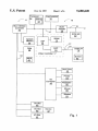
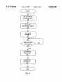
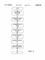
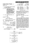
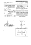
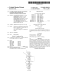
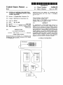
USO05680620A
United States Patent [191
[11] Patent Number:
[45] Date of Patent:
Ross
[54] SYSTEM AND METHOD FOR DETECTING
ACCESS TO A PERIPHERAL DEVICE USING
A DEBUG REGISTER
5,680,620
Oct. 21, 1997
Pentium Processor User’s Manual, vol. 3:Architectnre and
Programming Manual, Intel Corp., Chap. 17, Debugging,
pp. 17-1-17-9.
[75] Inventor: S. Timothy Ross, Georgetown, Tex.
Primary Examiner-Alvin E. Oberley
[73] Assignee: Dell USA, L.P., Round Rock, Tex.
Assistant Examiner—Kakali Chaki
Attomey, Agent, or Firm—-Skjerven, Morrill, MacPherson,
[21] Appl. No.: 497,515
Jun. 30, 1995
[22] Filed:
[5 1] Int. Cl.6 .................................................... .. G06F 11/00
395/704; 395/183.1; 395/835
[52] US. Cl. ........... ..
..................... .. 395/700, 183.1,
[5 3] Field of Search
Franklin & Friel L.L.P.; Stephen A. Terrile
[57]
In a microprocessor, a debug facility traps accesses to a
peripheral device, such as a speaker, residing at I/O port
addresses. In one embodiment, a number of debug registers
395/704, 835
are provided for a system or an application program to set a
trap at speci?c H0 or memory address, and to associate the
speci?ed address to an exception handling program. When
another application program accesses the speci?ed address,
References Cited
[56]
U.S. PATENT DOCUMENTS
5,537,536
ABSTRACT
for example to adjust the settings of a speaker, the exception
handling program is triggered to perform a speci?ed task,
7/1996 Groven ............................. .. 395/183.04
OI‘ HER PUBLICATIONS
such as to alert the program that the other application
program accessed the device it intended to monitor.
Pentium Processor User’s Manual, vol. 3: Architecture and
Programming Manual, @ Intel Corporation, 1983, Chapter
17, Debugging, pp. 17-1-17-9.
21 Claims, 6 Drawing Sheets
PROCESSOR
PROGRAM 1
PROGRAM 2
\ ——-
—'
RET
INT 1
HANDLER
_—
@?
IRET
\
36
I
1 14
DEVICE
47
US. Patent
Oct. 21, 1997
Processor
2
Sheet 1 of 6
Coprocessor
Debug
f‘ 11
1-8
L3-
I
f 10
Bus Interface
SCSI
Controller
Adapter
m
\14
k
_
_
_
_
%
_
System
I
I
I
ROM
I
DAC
§_8_
I
H
_
—
_/
SCSI
_
BIOS
_
_
_
I
Z.
I
I
77
i
79
_
_
DISPLAY
I
Z11
I
_
1
Screen
'
§g
i2.
Disk Drive
Q
Printer
I/O
ControIIer
Q
5
Keyggard
Mouse
Q
Modem
2
I/O Slot
E
I/C) Slot
Device
:12
41
U0 Slot
5L
HD
22
M
VSP
.7_0
| Video Controller 17
Q
0
I
Memory
3-6
44
/" 21
E
I
_
5,680,620
Fig_ 1
US. Patent
0a. 21, 1997
Sheet 2 of 6
lE_ E LE :R EL F EL
I
/R
G
NWNWNWNWOO
33221100
RESERVED
D
000
B B B
T S D
5,680,620
GLGLGLGGL
EE3322100DR7
B B B B
3 2 1 0
RESERVED
DR6
RESERVED
DR5
RESERVED
DR4
BREAKPOINT 3
LINEAR ADDRESS
DR3
BREAKPoINT 2
’
DR2
LINEAR ADDRESS
BREAKPOINT 1
[R1
LINEAR ADDRESS
BREAKPOINT 0
LINEAR ADDRESS
Fig. 2 _
DRO
US. Patent
0a. 21, 1997
Sheet 3 0f 6
SET ADDRESS
AS BREAKPOINT
1_09_
SET COR.
READNVRITE FIELD
1_02_
CALLBACK
ADDRESS
1%
BREAKPOINT
COND MET?
M
YES
SET STATUS
-
REGISTER
m
l
GENERATE ]
INTERRUPT
n;
Fig. 3
5,680,620
US. Patent
Oct. 21, 1997
(if-T“
Sheet 4 0f 6
DETERMINE
DEBUG REG
22
I
DETERMINE ADDRSS
IN DEBUG REG
1%;
Y
DETERMINE APP TO
NOTIFY
M
I
ACCESS CALLBACK
ROUTINE
1_2§
I
EXECUTE CALLBACK
ROUTINE
L8.
I
CALLBACK RETURN
E
I
IRET FROM DEBUG
EXCEPTION ROUTINE
E
I
FIG. 4
5,680,620
US. Patent
Oct. 21, 1997
_ Sheet 5 0f 6
PROCESSOR
_>
/"1
DEBUG REG.
DEBUG REG.
DEBUG REG.
DEBUG REG.
PROGRAM 1
1
2
3
4
PROGRAM 2
__
\_
INT 1
HANDLER
IRET _\
I
114
DEVICE
47
FIG. 5A
5,680,620
US. Patent
Oct. 21, 1997
Sheet 6 of6
5,680,620
PROCESSOR
PROGRAM 1
7
D
UG REG. 1
D
G. 3
PROGRAM 2
j;
\Q
21 E
INT1
HANDLER
-
IRET
I
5,680,620
1
2
SYSTEM AND METHOD FOR DETECTING
ACCESS TO A PERIPHERAL DEVICE USING
A DEBUG REGISTER
SUMMARY OF THE INVENTION
It has been discovered that using a debug facility to
provide information to a system or application program of
another program’s access to a shared resource allows the
BACKGROUND OF THE INVENTION
computer system to perform a noti?cation capability. Such
a system advantageously provides the shared resource,
1. Field of the Invention
The present invention relates to computer systems, and
more particularly to providing interrupt like capabilities to
input/output (I/O) devices which are used in computer
systems such as personal computer systems.
which may not have an interrupt capability, with an
interrupt-like capability Without modi?cation to or customi
10
zation to the system’s Basic Input/Output System (BIOS),
device drivers or existing hardware. Such a system also
2. Discussion of the Related Art
advantageously provides this function without the allocation
Personal computer systems in general and [BM compat
ible personal computer systems in particular have attained
of a hardware interrupt vector.
widespread use for providing computer power to may seg
detecting access to a device by an application program. The
More speci?cally, the invention relates to an apparatus for
ments of today’s modern society. A personal computer
apparatus includes a microprocessor which executes the
application program, a memory coupled to the microproces
system can usually be de?ned as a desk top, ?oor standing,
or portable microcomputer that includes a system unit (also
referred to as a host system) having a system processor and
associated volatile and non-volatile memory, one or more
diskette drives, and a ?xed disk storage device; the computer
20
system also includes a display, a keyboard, and a mouse
coupled to the system unit. One of the distinguishing char
acteristics of these systems is the use of a system board to
electrically connect these components together. These per
sonal computer systems are information handling systems
25
which are designed primarily to give independent computing
power to a single user (or a relatively small group of users
in the case of personal computers which serve as computer
server systems) and are inexpensively priced for purchase by
individuals or small businesses.
A computer system may also include one or a plurality of
I/O devices (i.e., peripheral devices) which are coupled to
the system processor and which perform specialized func
tions. Examples of 1/0 devices include modems, sound and
video devices or specialized communication devices. Often,
I/O devices may also include other devices coupled to them.
For example, a sound card may have a speaker coupled to it.
In a computer system, operating systems are used to
provide interface between applications programs which are
executed by the computer and the actual computer hardware.
An example of an operating system which operates with
personal computers includes the disk operating system
(DOS). Examples of multitasking operating systems or
environments include the 08/2 operating system and the
Windows family of operating systems and environments. It
is known to provide operating systems in which more than
one program can share a peripheral device.
When a computer system is executing an operating sys
35
sor and holding the application being executed by the
microprocessor and a debug register circuit coupled to the
microprocessor. The debug register circuit includes a break
point and a status indicator. The microprocessor monitors
the status indicator to determine when a peripheral device is
accessed The status indicator indicates that a peripheral
device has been accessed when the breakpoint is triggered
Additionally, the invention relates to a method of detect
ing access to a device in a computer system. The computer
system includes a microprocessor, a memory coupled to the
microprocessor and a debug register circuit coupled to the
microprocessor. The method includes the steps of: setting a
breakpoint in the debug register circuit to an address, the
address being called when access to the device is desired;
monitoring the breakpoint within the debug circuit to deter
mine whether the address is accessed; generating a device
access interrupt when the address is accessed; and executing
a debug interrupt service routine in response to the device
access interrupt being generated
The present invention is better understood upon consid
eration of the detailed description and the accompanying
drawings provided below.
BRIEF DESCRIPTION OF THE DRAWINGS
FIG. 1 shows a block diagram of a computer system in
accordance with the present invention.
FIG. 2 is a programmer’s model of the debug register
circuit of the Pentium microprocessor of the FIG. 1 com
puter system.
FIG. 3 shows a ?ow chart of the operation of a system for
detecting access to a device in accordance with the present
tem in which more than one program can share a peripheral 50 invention.
device, it is desirable to allow a program to detect access to
the peripheral device by another program. Thus allowing the
?rst program to be noti?ed of any changes to the device that
were performed by the second program. In the prior art, the
mechanism for passing information to the ?rst program
about the second program’s access of the peripheral device
is by way of the peripheral device’s device driver, or by
means of a software trap or exception under the protected
mode operation of the computer.
Often, however, this solution is inadequate. For example,
in the IBM compatible computer system architecture, the
audio speaker is not provided a capability to interrupt ?ie
processor and protected mode operation is not always avail
FIG. 4 shows a ?ow chart of the operation of the system
for detecting access to a device upon detection of access to
the device.
FIGS. 5A and 5B are block diagrams showing the inter
action of the various circuit elements of the system for
detecting access to a device of FIG. 3.
DETAILED DESCRIPTION
Referring to FIG. 1, personal computer system 10 is
shown. Computer system 10 includes processor 12, coupled
to local bus 14 which, in turn, is coupled to bus interface
controller 16, coprocessor 18, video controller 17 and small
able. Without a capability to generate a hardware interrupt,
computer system interface (SCSI) adapter 20. Processor 12
or the ability to use protected mode operation, detection of 65 is preferably a microprocessor from the family of x86
another program’s access to a common peripheral device is
processors, such as a Pentium microprocessor available
very di?icult, if not impossible.
from Intel Corporation, Santa Clara, Calif. Processor 12
5,680,620
3
4
includes debug register circuit 13 which includes a plurality
exception that is triggered when a speci?ed I/O or memory
of debug register locations.
address is accessed.
Local bus 14 includes conventional data, address and
control lines. SCSI adapter 20 couples local bus 14 to SCSI
As shown in FIG. 2, the Pentium microprocessor’s debug
register circuit 13 provides access to six debug registers
DRO-DR3 and DR6-DR7. Debug registers DR4-DR5 are
provided in the Pentium microprocessor for software com
patibility reasons. Use of debug registers DR4-DR5 is not
recormnended by the manufacturer of the Pentium proces
bus 21 to which SCSI devices such as a SCSI hard drive 22
may be coupled. Host unit 11 includes system memory 36,
non-volatile memory 38 and I/O controller 40, which are all
coupled to bus interface controller 16.
sor. Debug registers DRO-DR4 can each hold an I/O or
Bus interface controller 16, which is also referred to as
core logic, may include one or a plurality of integrated 10 memory address as a breakpoint. The conditions for gener
ating a debug exception in the Pentium microprocessor is
circuits. Bus interface controller 16 performs at least two
speci?ed in the Debug Control Register, which is debug
register DR7.
Debug control Register DR7 includes (i) four 2-bit read/
primary functions. The ?rst function that bus interface
controller 16 performs is as a memory controller for access
ing main system memory 36 and nonvolatile memory 38.
Main system memory 36 is a dynamic random access
write ?elds (R/Wtl-RW3), each corresponding to one of the
debug registers DRO-DR3; (ii) four 2-bit length ?elds
(LENO-LEN3), each specifying the range (in bytes) of the
memory (RAM) which may include one or more single,
in-line memory modules (SIMMS) and stores programs and
data for execution by system processor 12 and coprocessor
18. Nonvolatile memory 38 is, e.g., a read only memory
speci?ed I/O or memory address within which the break
(ROM) which stores microcode including the basic input
output system (BIOS) 42 of computer system 10.
BIOS 42 is a microcode software interface between an
operating system or application programs and the hardware
of system 10. The operating system and application pro
grams access BIOS 42 rather than directly manipulating I/O
ports and control words of the speci?c hardware. BIOS 42
is accessed through an interface of software interrupts and
contains a plurality of entry points corresponding to the
different interrupts. In operation, BIOS 42 is loaded from
ROM 38 to system memory 36 and is executed from system
memory 36.
The second function that bus interface controller 16 20
performs is as an interface between bus 14 and input/output
(110) bus 44. 110 bus 44 conforms to the industry standard
architecture (ISA) standard, which is also sometimes
25
When the condition speci?ed for a breakpoint is met, the
satis?ed condition is reported in Debug Status Register
DR6. Debug Status Register DR6 includes four l-bit ?elds
Bil-B3 each of which is set when the conditions for the
35
operation of disk drive 52, printer 54, keyboard 56 and
desired. This address is provided by the program desiring the
50
79. Display 78 includes screen 80 on which video informa
55
monitoring, e.g., program 2 in FIG. 5A. Next at read/write
step 102, the read/write ?eld which corresponds to the
breakpoint register is set to indicate that both reads and
writes to the address corresponding to the breakpoint should
cause the breakpoint to be tripped, i.e., cause an indication
that the breakpoint has been accessed Next, at callback
address step 104, the callback address of the routine to be
called is stored within debug table 106 within memory 36.
This callback address is the address which indicates where
to transfer control when the device corresponding to the
stored breakpoint is accessed by another program, e.g.,
program 1.
After the system is initialized, the system transfers to a
reference to the debug registers of the Pentium
monitor mode of operation. During the monitor mode, as
microprocessor, which is available from Intel Corporation,
Santa Clara, Calif; these debug registers are an example of
the arrangement of registers within debug register circuit 13.
indicated by monitor step 108, the breakpoint register is
The de?ned use of the debug registers of the Pentium
register circuit 13. The breakpoint is a trap or software
satis?ed.
100. The address which is set as a breakpoint corresponds to
the address which is called when access to the device is
mouse 58. 110 controller 40 also includes a modem port to
which a modem 59 may be optionally connected.
microprocessor is described in detail in Chapter 17,
“Debugging”, Pentium Processor User’s Manual, Vol. 3:
Architecture and Programming Manual, available from Intel
Corporation. According to the present invention, a system or
application program speci?es a breakpoint in the debug
corresponding one of the debug registers DRO-DR3 is
Referring to FIGS. 3, 5A and 5B, according to the present
invention, the system for detecting access to a peripheral
device is initiated by setting an address as a breakpoint and
storing that value within one of the breakpoint locations of
debug register circuit 13 at set address as breakpoint step
to 110 controller 40, and a plurality of I/O slots 46, into
which a variety of I/O or expansion cards or devices, e.g.,
device 47 may be inserted.
I/O controller 40 is also coupled to and controls the
tion is presented.
Referring to FIG. 2, the present invention is illustrated by
(v) a GD bit which protects access to the debug registers. In
the Pentium microprocessor, when the “DE” bit of the CR4
register is set, the Pentium microprocessor is operating
under the “debug extension” mode, which allows I/O port
addresses to be speci?ed in the debug registers DRO-DR3.
referred to as the AT bus standard. Bus 44 is fm'ther coupled
Video controller 17, which is coupled to local bus 14,
includes video signal processor (VSP) 70, video RAM
(VRAM) 72 and digital to analog converter (DAC) 74.
Video signal processor 48 is coupled to video RAM
(VRAM) 60 and to digital to analog converter (DAC) 62.
Digital to analog converter 66 is coupled display terminal
77. Display 78, which is a computer display device con
forming to, e.g., the super video graphics array (SVGA)
standard, is coupled to display terminal 77 via display cable
point is effective; (iii) four l-bit “local” ?elds, each indi
cating that the breakpoint condition set in the corresponding
debug register DRO-DR3 causes a breakpoint only in the
current task; (iv) four l-bit “global” ?elds, each indicating
that the breakpoint condition set in the corresponding debug
register DRO-DR3 is preserved across task boundaries; and
65
monitored by processor 12 to determine whether the break
point has been triggered, as indicated by the address location
which is held as the breakpoint value being accessed. While
the breakpoint has not been accessed, processor 12 contin
ues to monitor the breakpoint register. When the breakpoint
is triggered, as indicated by an address equaling the break
point value, then control transitions to status step 110. At
status step 110, the status register which corresponds to the
5,680,620
5
6
tripped breakpoint register is set. When processor 12 detects
down program to transfer from a monitor powered-down
mode of operation to a monitor powered-up mode of opera
this register being set, then processor 12 generates a device
access interrupt, which is a reserved debug interrupt, INTl,
at generate interrupt step 112. This device access interrupt
tion. After this transfer, control then returns to the interrupt
causes processor 12 to access and execute debug interrupt
speaker is diiferent from the breakpoint for changing the
service routine. Because the breakpoint for access to the
service routine 114, i.e., an interrupt handler routine.
Referring to FIGS. 4 and 5B, debug interrupt service
speaker drive frequency, a change in the speaker driving
frequency does not necessarily cause access to the callback
routine starts by determining which debug register caused
the debug interrupt to be generated at debug step 120. After
system 10 determines which debug register caused the
interrupt to be generated, this register is accessed to deter
routine within the monitor power-down program.
Thus, the present invention assures the monitoring system
10
another program to the shared resource. This noti?cation
mine the address which caused the interrupt at determine
address step 122. After the address is determined, thus
indicating which device was accessed, then system 10
determines which application to notify by using the callback
address entry of debug table 106 which corresponds to the
accessed address at determine application step 124. This
entry was programmed during store callback address step
104 (see FIG. 3). After the callback address is determined,
capability is provided without the use of extra or dedicated
hardware resource, such as a processor interrupt capability.
15
The above detailed description is provided to illustrate the
variations within the scope of the present invention are
possible.
For example, the present invention is applicable not only
to the Intel x86 family of microprocessors, but also any
callback routine performs a function which is desired as a
result of detecting an access to the device. After the callback
step 130. The interrupt handler routine then continues
microprocessor having a debug facility which allows setting
25
executing until reaching at lREI‘ step 132, the interrupt
described with reference to an I/O bus conforming to the ISA
which originally caused generation of the interrupt, e.g.,
bus standard, it is contemplated that other bus architectures
such as the peripheral connect interface (PCI) bus
architecture, ?'re Microchannel architecture (MCA), the
_
For example, in one embodiment, program 1 is an elec
tronic mail program which causes a speaker to sound when
Extended Industry Standard (EISA) bus architecture, the
mail is received by the program. Program 2 is another
program such as a monitor power-down program which is
35
operating in parallel with program 1. When mail is received
while program 2 is operating to place computer system 10 in
a monitor powered-down mode of operation, then via the use
of the present invention, computer system 10 may cause
Program 2 to exit the monitor powered-down mode of
operation. More speci?cally, when the speaker is accessed,
a microprocessor, the microprocessor executing the ?rst
40
interrupt handling program completes, it transfers control
back to Program 1, which continues with its operation.
More speci?cally, the I/O port address for a peripheral
50
?eld (i.e. R/W0 for debug register DRO) in the Debug
Control Register DR7 set to the bit pattern ‘10’, which
indicates that the breakpoint is tripped when port address
61H is read or written. In the case of when a speaker is 55
driven by the accessing application, the driving frequency is
holding the ?rst and second application programs being
executed by the microprocessor;
a debug register circuit coupled to the microprocessor, the
debug register circuit including a breakpoint and a
status indicator, the microprocessor monitoring the
is accessed by the ?rst application program, the status
indicator indicating to the second application program
that a peripheral device has been accessed by the ?rst
application program when the breakpoint is triggered
2. The apparatus of claim 1 wherein
the breakpoint is triggered when a predetermined address
location is accessed, the predetermined address loca
tion corresponding to a memory address location.
3. The apparatus of claim 1 wherein
the breakpoint is triggered when a predetermined address
location is accessed, the predetermined address loca
tion corresponding to an input/output address location.
4. The apparatus of claim 1 wherein
the debug circuit includes a plurality of breakpoints and a
speci?ed in a timer (‘Timer 2”) of the core logic.'Another
one of the debug registers DRO-DR3 can be provided the
I/O port address of Timer 2, so that any change in the driving
frequency may also cause a debug exception.
When a debug exception due to an access to the speaker
breakpoint occurs, the reserved debugger interrupt INTI is
generated at microprocessor 12. To service this reserved
accesses a callback routine within the monitor power-down
program. This callback routine causes the monitor power
application program and a second application program;
a memory coupled to the microprocessor, the memory
status indicator to determine when a peripheral device
registers DRO-DR3, say DRO, with the corresponding R/W
debugger interrupt, processor 12 executes a debug interrupt
service routine. The debug interrupt service routine then
NuBus bus architecture or the UniBus bus architecture may
be used.
I claim:
1. An apparatus for detecting access to a device by ?rst
application program, the apparatus comprising:
the callback address which is stored within debug table 106
calls a portion of Program 2 which causes the desired action,
e.g., the exit from the monitor powered-down mode of
operation. After this is accomplished, then program 2 issues 45
a return to the INTI interrupt handling program. After the
device, such as 61H for the speaker, is set in one of the debug
of breakpoints in an instruction execution stream based on
access to a speci?ed address. The ‘present invention is
de?ned by the following claims.
Also for example, while the preferred embodiment is
return (IREI‘) instruction, which instructs processor 12 to
return from the interrupt handler routine to the program
program 1.
OTHER EMBODIMENTS
speci?c embodiments of the present invention and is not
intended to be taken as limiting. Various modi?cations and
this address is accessed at access callback routine step 126
and the callback routine which is stored at the callback
address is executed at execute step 128. Executing the
routine is complete, the control transfers to callback return
program or application of noti?cation upon an access by
corresponding plurality of status indicators, each break
point and corresponding status indicator providing the
65
ability to indicate access to a di?erent I/O' device.
5. A system for detecting access to a device, the system
comprising
5,680,620
8
7
13. The method of claim 11 wherein:
a microprocessor, the microprocessor operating with a
?rst application and a second application;
a memory coupled to the microprocessor, the memory
the computer system includes a plurality of applications
accessing the device the debug interrupt service routine
includes the steps of
determining which one of the plurality of applications
to notify based upon the callback address;
transferring control to a location indicated by the
storing a debug interrupt service routine for providing
notice to the ?rst application that the second application
has accessed a device address;
a debug register circuit coupled to the microprocessor;
means for setting a breakpoint in the debug register circuit
by the ?rst application to an address, the address being
callback address; and
called when access to the device is desired;
means for monitoring the breakpoint within the debug
circuit to determine whether the address is accessed;
and
transfen'ing control back to the debug interrupt service
means for generating a device access interrupt when the 15
point locations, and
device access interrupt being generated.
the debug interrupt service routine includes the steps of:
determining which of the plurality of breakpoint loca
6. The apparatus of claim 5 wherein
the breakpoint is triggered when a predetermined address
location is accessed, the predetermined address loca
tions caused the generation of the device access
interrupt; and
tion corresponding to a memory address location.
7. The apparatus of claim 5 wherein
25
transferring control to the callback address location;
and
wherein the method further includes the steps of execut
35
address, the address being called when access to the
device is desired;
monitoring the breakpoint within the debug circuit to
determine whether the address is accessed;
generating a device access interrupt when the address is
accessed; and
executing a debug interrupt service routine in response to
the device access interrupt being generated, wherein
the debug interrupt service routine provides notice to a
?rst application program that the device was accessed
by a second application program.
10. The method of claim 9 further comprising the steps of:
setting a status indication when the address is accessed,
the setting a status indication causing the processor to
generate the device access interrupt of the generating a
device access interrupt step.
11. The method of claim 9 wherein
the setting the breakpoint is part of an initializing step,
and wherein the initializing step further includes the
step of
storing a callback address, the callback address indicating
where to transfer control when the breakpoint is
accessed
12. The method of claim 11 wherein
the register circuit includes a read write ?eld; and the
initializing step further includes the step of
setting the read write ?eld to indicate that both reads and
writes to the address corresponding to the breakpoint
cause the breakpoint to be tripped.
determining the address set as the breakpoint for the
breakpoint location which caused the generation of
the device access interrupt.
15. The method of claim 14 wherein
the debug interrupt service routine further includes the
steps of:
determining which application to notify based upon the
callback address;
ability to indicate access to a different I/O device.
9. A method of detecting access to a device in a computer
system, the computer system including a microprocessor, a
memory coupled to the microprocessor and a debug register
circuit coupled to the microprocessor, the method compris
ing the steps of:
setting a breakpoint in the debug register circuit to an
routine.
14. The method of claim 11 wherein
the debug register circuit includes a plurality of break
address is accessed, the microprocessor executing the
debug interrupt service routine in response to the
the breakpoint is triggered when a predetermined address
location is accessed, the predetermined address loca
tion corresponding to an input/output address location.
8. The apparatus of claim 5 wherein
the debug circuit includes a plurality of breakpoints and a
corresponding plurality of status indicators, each break
point and corresponding status indicator providing the
'
wherein the method further includes the steps of
executing a callback routine after control is transferred to
the callback address location; and
ing the callback routine, and transferring control back
to the debug interrupt service routine.
16. A computer system comprising:
a microprocessor, the microprocessor running a plurality
of applications;
a memory coupled to the microprocessor;
a debug register circuit coupled to the microprocessor;
means for setting a breakpoint in the debug register circuit
to an address, the address being called when access to
a device is desired;
means for storing a callback address, the callback address
indicating where to transfer control when the break
point is accessed;
means for monitoring the breakpoint within the debug
circuit to determine whether the address is accessed;
means for generating a device access interrupt when the
50
address is accessed;
means for executing a debug interrupt service routine in
response to the device access interrupt being generated,
wherein the debug interrupt service routine determines
which one of the plurality of applications to notify
55
based upon the callback address and transfers control to
a location indicated by the callback address;
means for executing a callback routine after control is
transferred to the location indicated by the callback
address; and
means for transferring control back to the debug interrupt
service routine.
17. The computer system of claim 16 further comprising:
a read/write ?eld in the debug register circuit; and
means of setting the read/write ?eld to indicate that both
reads and writes to the address corresponding to the
breakpoint cause the breakpoint to be tripped.
5,680,620
9
10
18. The computer system of claim 16 wherein
wherein the debug interrupt service routine determines
which of the plurality of breakpoint locations caused
the generation of the device access interrupt and deter
the debug register circuit includes a plurality of break
points and a corresponding plurality of status
indicators, each breakpoint and corresponding status
mines the address set as ?ie breakpoint for the break
point location which caused the generation of the
device access interrupt, and wherein the debug inter
indicator providing the ability to indicate access to a
di?ierent address location.
19. A computer system comprising:
a microprocessor, the microprocessor running a plurality
of applications;
a memory coupled to the microprocessor;
a debug register circuit coupled to the microprocessor, the
rupt service routine further determines which one of the
plurality of applications to notify based upon the call
back address and transfers control to the callback
10
debug register circuit including a plurality of break
point locations;
means for setting a breakpoint in the debug register circuit
15
to an address, the address being called when access to
a device is desired;
means for storing a callback address, the callback address
means of setting the read/write ?eld to indicate that both
reads and writes to the address corresponding to the
breakpoint cause the breakpoint to be tripped.
21. The computer system of claim 19 wherein:
the debug register circuit includes a plurality of break
points and a corresponding plurality of status
indicating where to transfer control when the break
point is accessed;
means for monitoring the breakpoint within the debug
circuit to determine whether the address is accessed;
indicators, each breakpoint and corresponding status
means for generating a device access interrupt when the
address is accessed; and
means for executing a debug interrupt service routine in
response to the device access interrupt being generated,
address location; and
means for executing the callback routine, and
means for transferring control back to the debug interrupt
service routine.
20. The computer system of claim 19 further comprising:
a read/write ?eld in the debug register circuit; and
25
indicator providing the ability to indicate access to a
di?‘erent address location.
*
*
*
*
*