1
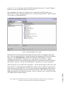
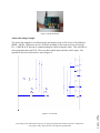
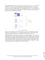
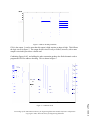
Teaching Address/Data Demultiplexing for Microcontrollers using Lattice
Semiconductor ispDesignEXPERT Starter Kit
Eric Clark, Kevin Torres, David Loker
Penn State Erie, The Behrend College
Abstract
Laboratory experimentation can be a very important part of the learning experience for students.
Particularly for microcontroller courses that involve hardware. In Electrical Engineering
Technology, lab time is utilized in every course. Experiments involving microcontrollers can
account for a lot of time in wiring basic components. Decoding a 16-bit address alone would
involve hand wiring 6 logic gates. This would easily take up one lab period itself, assuming the
decoding design is correct. Using the Lattice Semiconductor ispDesignEXPERT software, the
address decoding can be accomplished using schematic capture and programmed to a
programmable logic device (PLD). A student can easily simulate their design in software before
going to the hardware. The ispDesignEXPERT allows the user to view the input and output
waveforms of the schematic design. Alterations can be made to the schematic and the waveform
editor will adjust accordingly. This tool will also be used to teach address/data demultiplexing
commonly used in Intel 8051 based microcontrollers for I/O memory-mapping. The
ispDesignEXPERT allows more efficient microcontroller experiments to get conducted in a
semester providing a better understanding of their function to the students.
Introduction
This paper describes the tools for programmable logic devices (PLD) and Lattice
DesignEXPERT software as applied to microcontroller education. A simple example is given to
become familiar with the software and how to program the PLD. Then an address decoding
design circuit will be implemented to interface with a microcontroller.
At Penn State Erie, Intermediate Microcontrollers EETBD 455 is taught. This course uses the
C508 Infineon microcontroller which is Intel 8051 based. For software and simulation the C51
tools from Keil Software are used. Simulation or hardware labs accompany lectures every week.
In lab, software is written in assembly language and then downloaded to a microcontroller. In
the more advanced labs, logic gates are used for address decoding. These were hand wired using
wire wrap techniques.
Page 7.1059.1
Proceedings of the 2002 American Society for Engineering Education Annual Conference & Exposition
Copyright Ó 2002, American Society for Engineering Education
Using a Lattice Mach4 PLD and DesignEXPERT software, all the logic gates would be
programmed into the PLD saving valuable laboratory time. Another advantage is fast design
time. Faster changes can be made and simulated with the software than wire wrapping.
LED Example
From Lattice Semiconductor Corporation University Program, ispStarter Kits part# Mach4-sk44
can be obtained. These kits include:
· IspDesignEXPERT Starter and ispVM System software
· 44-pin in-system programming (isp) board with LED display
· ispDOWNLOAD cable with 10 pin JTAG Connector
· (2) MACH4 sample devices
· Full documentation and user manuals
There are four seven segment LEDs on the isp board. This example will take advantage of all
four. The name “Eric” will be displayed, one character for each LED. Along with the LED
displays the board offers three push button switches. The example was designed to display
“Eric” when both SW1 and SW2 are pushed, and only when these two are pushed together.
Figure 1 shows the schematic that will display “Eric.” It was designed in the schematic editor of
the DesignEXPERT software. Reference Appendix A for instructions on designing circuits
within the editor.
Figure 1: Schematic for LED decoding
Proceedings of the 2002 American Society for Engineering Education Annual Conference & Exposition
Copyright Ó 2002, American Society for Engineering Education
Page 7.1059.2
Inputs are indicated by a1 and a2. Outputs are o1, o2, o3, o4, o5, o6, o7, o8, o9, o10, and o11.
Two input OR gates were chosen for all outputs. Each output represents one segment of an LED
display. a1 and a2 are later assigned to SW1 and SW2 of the isp board respectively. All the
outputs are connected in parallel so that they all come on at the same time. Figure 1 is organized
so that o1, o2, o3, o4, and o5 are for the first LED and display the letter E. o6 and o7 display a
lowercase r on the second LED, and so on with the rest.
Once completed in the editor, the schematic can be complied for the PLD. In this case a
MACH4 32/32 is used. Reference Appendix A for starting ispDesignEXPERT. Figure 2 shows a
screen capture of ispDesignEXPERT.
Figure 2: ispDesign EXPERT screen capture
Before the PLD can be programmed, the inputs and outputs need to be assigned to the proper
pins. This is an important process. Without the proper pin assignment the PLD will not operate
as desired. The Constraint Editor will allow for the proper pin assignment. Reference
“Running Constraint Editor” in Appendix A for operating the constraint editor. There is
documentation with the starter kit that specifies which pins correspond to which LED segments
and switches. Reference “Pin list for the ISP Board” in Appendix A for the pin assignments.
After the pin-outs are set, double-click “Fit Design”. This checks the design to make sure it will
fit on the PLD. It will also generate a JEDEC File. On the screen, as in figure 2, a green check
will be present next to JEDEC File. This is the file needed for programming the PLD in the isp
board. The LatticePRO software needs to be started to continue. This is done by going to the
Tools pop down menu and clicking on its name. Reference Appendix A for running LatticePRO.
The working PLD is shown in figure 3.
Page 7.1059.3
Proceedings of the 2002 American Society for Engineering Education Annual Conference & Exposition
Copyright Ó 2002, American Society for Engineering Education
Figure 3: ISP Starter Board
Address Decoding Example
The goal in this example is to address decode and memory map an I/O device to the addresses
8000H – 8001H. Without the use of a PLD this decoding circuit requires the use of six logic
ICs. A DM74LS138 Decoder is simulated using the Lattice schematic editor. This will allow it
to be programmed into the PLD. There are three enable inputs and three select inputs. The
equivalent circuit for the decoder is seen in figure 4.
Figure 4: 3-8 Decoder
Page 7.1059.4
Proceedings of the 2002 American Society for Engineering Education Annual Conference & Exposition
Copyright Ó 2002, American Society for Engineering Education
The address 8000H can be converted to binary. It will result in 16-bits, A15 –A0, 1000 0000
0000 0000B. In this case, A15 is the only high level and will be connected to the G1 pin of
figure 3. A0 – A2 are assigned to connect to the A, B, and C select pins. A0 – A2 will also be
used to select one of the eight I/O addresses. The remaining 12-bits, A3 – A14 are all low levels,
therfore, are all OR’ed together as seen in figure 5. This is then connected to G2A of figure 4.
Finally, G2B is connected directly to ground.
Figure 5: Address Decoding
Figure 5 can be simulated in the Lattice software also. This will save valuable time in design
and wiring. As seen in figure 4, A3 – A14 represent inputs to the PLD. These inputs can be
assigned to specific pins of the PLD. The OR gates are internal to the PLD. The
ispDesignEXPERT software also allows the user to view timing simulations. Test vectors are
provided by the user, and the software will output the waveforms. In figure 5 there are 12 inputs,
it is possible to run through all the combinations of logic and view all the outputs. This would
make for 4096 combinations. This provides the user with a quick way to troubleshoot a design.
Using all OR gates as above the output will always be high except when all the inputs are low.
Figure 6 shows a few of the combinations and the output at those levels. Reference “Creating
waveforms and test vectors” Appendix A for waveform simulation.
Page 7.1059.5
Proceedings of the 2002 American Society for Engineering Education Annual Conference & Exposition
Copyright Ó 2002, American Society for Engineering Education
Figure 6: Address decoding simulation
G2A is the output. It can be seen that this output is high anytime an input is high. This follows
the logic circuit in figure 5. The output for this circuit is easy to follow, however, with a more
complex circuit this provides a valuable tool.
Combining figures 4 & 5, and adding the other constraints produce the final schematic used to
program the PLD for address decoding. This is shown in figure 7.
Proceedings of the 2002 American Society for Engineering Education Annual Conference & Exposition
Copyright Ó 2002, American Society for Engineering Education
Page 7.1059.6
Figure 7: Combined circuit
The outputs Y0 – Y7 are used as chip enables signals for addresses 8000H – 8007H. Figure 8
shows the output enables for addresses 8000H – 8002H. Reference “Creating waveforms and test
vectors” Appendix A for waveform simulation. In order to memory map an I/O device to these
addresses, Y0 is then ANDed with the WRITE signal from the micrcontroller to geneartate a
memory WRITE cycle. Y1 can be ANDed with the READ signal from the micrcontroller to
geneartate a memory READ cycle.
Figure 8: Simulation for combined circuit
Conclusion
One method of simplifying hardware circuits in microcontroller labs is to introduce PLDs for
logic design. By using Lattice Semiconductor ispDesignEXPERT software a logic circuit can be
designed and simulated. The simulation capability makes it easier for students to visualize the
timing diagrams of the signals invloved. This helps explain memory mapping I/O devices for
data READ and data WRITE instructions. The logic design are all done in softare which makes
for rapid prototyping as the students troubleshoot their circuits as they design for example an
interface for a liquid crystal display. The use of PLDs also reduces the amount of wirewapping
and increases the reliability of the circuit.
Acknowledgements
The authors would like to thank Mr. Tim Schnettler, Design Tools Marketing Manager with
Lattice Semiconductor Corporation.
Page 7.1059.7
Proceedings of the 2002 American Society for Engineering Education Annual Conference & Exposition
Copyright Ó 2002, American Society for Engineering Education
Bibliography
Design Verification Tools User Manual Version 8.0, Copyright December 1999
Lattice Semiconductor Corporation
Schematic Entry User Manual Version 8.0, Copyright December 1999
Lattice Semiconductor Corporation
ispDesignExpert Tutorial Version 8.0, Copyright December 1999
Lattice Semiconductor Corporation
ERIC CLARK
Eric Clark is a senior in the Electrical Engineering Technology Program at Penn State Erie. He expects to receive
his B.S. degree in Electrical Engineering Technology from Penn State Erie May of 2002.
KEVIN TORRES
Kevin M. Torres is a lecturer in engineering and received the B.E.E. degree (Cum Laude) from Auburn University
in 1990, and the M.S.E.E. degree from Georgia Institute of Technology in 1996. In 1990 he joined Georgia Tech
Research Institute (GTRI) as a research engineer. In 1998, he joined the faculty at Penn State Erie, in the Electrical
Engineering Technology Program. Since 1998 he has been teaching courses in C++, Intermediate Microcontrollers
and Advanced Microcontrollers. He is a member of IEEE, IMAPS, and ASEE.
DAVID LOKER
David R. Loker is an assistant professor of engineering and received the B.E.E. degree from Gannon University in
1984, and the M.S.E.E. degree from Syracuse University in 1986. In 1984, he joined General Electric (GE)
Company, AESD, as a design engineer. While at GE, Mr. Loker was primarily involved in the design and
development of military communication systems. In 1988, he joined the faculty Penn State Erie, in the Electrical
Engineering Technology Program. Mr. Loker's research interests include PC-based control systems, communication
systems, and instrumentation systems.
Page 7.1059.8
Proceedings of the 2002 American Society for Engineering Education Annual Conference & Exposition
Copyright Ó 2002, American Society for Engineering Education
Appendix A
Installing Lattice Starter Software from CD ROM
1.
2.
3.
4.
Open file folder of disk and start “setup.exe”.
Click on the install button and continue to follow setup instructions.
Be aware that it will take up 610MB of space on your hard disk.
Reboot your PC to finalize the install
Obtain License file
1. Go to website www.latticesemi.com
2. Click on licensing on the left side.
3. You’ll see a list; you want a starter license for ispDesignEXPERT-Starter
4. Next, request a license, you need to provide your hard disk serial number. Follow on
screen instructions. To get your hard disk serial number go to DOS prompt, and type vol
c:
5. The file will be sent immediately to your email address.
6. Save this file as “license.dat” in C:\ispTOOLS\ispcomp\license
Starting ispdesignEXPERT
1.
2.
3.
4.
Go to Start/Lattice Semiconductor/ispdesignEXPERT
Go to File/ New Project. Save it in the student directory
screen is divided into two columns. (Sources in project, and Processes for current source)
We need to select the proper device. Under the Sources in Project, double click on
ispLS15384VA-125LB388.
5. A window will pop open. Under family, scroll down until it says “Mach 4”. The device
number and part name are written on the PLD itself. You will see either M4-32/32 or
M4-64/32 which indicates the device. Under that is the part number which ends in JC or
JI. When selecting the part number choose the one ending in JC. Click OK and the
device is selected correctly. A window may pop open to suggest another device click
“OK” and then “YES” for continue with operation.
Starting Schematic Editor
Proceedings of the 2002 American Society for Engineering Education Annual Conference & Exposition
Copyright Ó 2002, American Society for Engineering Education
Page 7.1059.9
1. Go to the "Window" pop down menu and select Schematic Editor. You will see a
window pop open.
2. To add a logic gate, go to Add menu and select symbol.
3. A window pops opens. You will see a list of libraries. Make sure \generic\gates.Lib is
highlighted.
4. A list of symbols will be shown. The number in front of the logic names identifies how
many inputs. The number after the logic name shows how many of those inputs are
inverted. ex. (G_3AND1 means a 3 input AND gate with one inverted)
5. For wiring, go to Add menu and select wire. Click on end points and double click to
complete connection. Right click mouse to end wiring.
6. Before a wire can be labeled an input or output, it must first be given a 'Net Name'. To
do so, Add menu and select net name.
7. You will see at the bottom of the schematic editor window a cursor blinking where it
says, Enter Net Name=.
8. Create a name and hit enter.
9. Now, the 'net name' is attached to the mouse. Move the mouse to the location you want
to name. (this is usually at the end of wires)
10. Left click on the spot you want to put it and hold. Now drag it out a bit, and unclick.
You will see that the wire extended and the 'Net Name' was placed in front of it.
11. After all the wires are labeled with 'Net Names', go to Add menu and select I/O Marker.
12. A window will pop open with four options. Mark all the 'net names' as input or output.
To do so, click at the end of wire right in front of the 'net name'. If done correctly, a box
will be drawn around the net name and pointing in the direction, you desired.
13. Save and close Schematic Editor.
Import Schematic into Design
1. While in the ispDesignEXPERT Project Navigator window, go to Source menu and
select Import.
2. Go to the folder you saved it. Click it and hit open.
3. It will appear in the left column under sources in project. Click on it.
Create Simulation File and Import it
1. Another set of processes will show up on the right. We are interested in the process
'ABEL Test Vector Template'.
2. Double click and it will pop open a new window.
3. Go to File menu and select Save As. Save it to the same file as your schematic. The
default file extension is *.abt. This needs to be changed to .abv. ¨¨If this is not done,
the program will not work.¨¨
4. To import it, go Source menu and select Import. Open the file you just created with the
.abv extension name. It will appear in the left column under sources in project.
Proceedings of the 2002 American Society for Engineering Education Annual Conference & Exposition
Copyright Ó 2002, American Society for Engineering Education
Page 7.1059.10
Creating waveforms and test vectors
1. Double click on the Test Vector Template you just made. It will bring open a text editor
window.
2. Scroll down to Test_vectors. The test vectors need to be manually added.
3. Example: if the given test_vector template is ([input1, input2] -> [Output])
The tests needed then are
[0,0] -> [.R.];
[0,1] -> [.R.];
[1,0] -> [.R.];
[1,1] -> [.R.];
The .R. is a code that produces the proper output depending on the input conditions. Save
and close.
4. The 0 and 1 combinations are all the possible logic conditions of the example circuit.
5. Back in the project navigator, with this file highlighted, there will be a list of processes
on the right side. Double click Compile Test Vectors.
6. Once completed double click Timing Simulation.
7. Simulator Control Panel window will open. Go to Simulate menu and select Run.
8. This will open the Waveform Editor window showing all the test vectors conditions
given.
9. The test vectors used that generate figure 5 are shown below.
([A9,A8,A7,A6,A5,A4,A3,A14,A13,A12,A11,A10] -> [G2A])
[0,0,0,0,0,0,0,0,0,0,0,0] -> [.R.];
[0,0,1,0,0,0,0,0,0,0,0,0] -> [.R.];
[0,0,0,0,1,0,0,0,0,1,0,0] -> [.R.];
[0,0,1,0,0,0,0,0,0,0,0,1] -> [.R.];
[1,1,1,1,1,1,1,1,1,1,1,1] -> [.R.];
10. The test vectors used that generate figure 8 are shown below.
([A15,A14,A13,A12,A11,A10,A9,A8,A7,A6,A5,A4,A3,A2,A1,A0] ->
[Y7,Y6,Y5,Y4,Y3,Y2,Y1,Y0])
[0,0,0,0,0,0,0,0,0,0,0,0,0,0,0,0] -> [.R.,.R.,.R.,.R.,.R.,.R.,.R.,.R.];
[1,0,0,0,0,0,0,0,0,0,0,0,0,0,0,0] -> [.R.,.R.,.R.,.R.,.R.,.R.,.R.,.R.];
[1,0,0,0,0,0,0,0,0,0,0,0,0,0,0,1] -> [.R.,.R.,.R.,.R.,.R.,.R.,.R.,.R.];
[1,0,0,0,0,0,0,0,0,0,0,0,0,0,1,0] -> [.R.,.R.,.R.,.R.,.R.,.R.,.R.,.R.];
END
Running Constraint Editor
1. While in ispDesignEXPERT project navigator, double click Constraint Editor. This
will open another window.
2. Go to Edit menu and select Location Assignment.
3. In Filter section, make sure Input and Output/Bidi are checked.
4. Select a signal from the list, and then under Assignment select the desired pin number . A
list of the pins for the isp board is given in the kit and at the bottom of this appendix.
5. When this combination is met, click the Add button and it will be added the existing pin
list at the bottom.
6. Repeat for all the pins you wish to control.
7. Click OK and close.
8. Back on in the ispDesignEXPERT project navigator; double click Fit Design to compile
the whole project.
Page 7.1059.11
Proceedings of the 2002 American Society for Engineering Education Annual Conference & Exposition
Copyright Ó 2002, American Society for Engineering Education
Running LatticePRO
1. While in ispDesignEXPERT project navigator go to Tools pop down menu and select
LatticePRO Software. This will pop open a new window.
2. Start a new file. Once that is complete go to Edit menu and select Add Device.
3. Under part name, click on Select Part. This will open a new window.
4. Device Family needs to be set to MACH4XX. There are 2 devices provided with the
starter kits - M4 32/32 and M4 64/32. Make sure in Device the correct one is selected for
the one you’re using. Package stays at 44-pin PLCC. Click OK and close.
5. JTAG Operation needs to be set to the operation we want. Select P for erase, program &
verify Device w/JEDEC file. Always use this case.
6. Specify where the JEDEC file is. This file was generated automatically when Constraint
Editor and Fit Design were run.
7. Click Ok and window will close.
8. A GO button will be lit; click on it and that will program it.
Page 7.1059.12
Proceedings of the 2002 American Society for Engineering Education Annual Conference & Exposition
Copyright Ó 2002, American Society for Engineering Education
Pin list for the ISP Board
Pin Definition
GND
I/O 0
I/O 1
I/O 2
I/O 3
I/O 4
I/O 5
I/O 6
I/O 7
TDI
CLK 0 / I O
GND
TCK
I/O 8
I/O 9
I/O 10
I/O 11
I/O 12
I/O 13
I/O 14
I/O 15
VCC
GND
I/O 16
I/O 17
I/O 18
I/O 19
I/O 20
I/O 21
I/O 22
I/O 23
TMS
CLK 1 / I 1
GND
TDO
I/O 24
I/O 25
I/O 26
I/O 27
I/O 28
I/O 29
I/O 30
I/O 31
VCC
MACH Inputs
LED
Comment
SW 1
U24 - A
U24 - B
U24 - C
U24 - D
U24 - E
U24 - F
U24 - G
U24 - H (DP)
Use as Input only
CK0 Clock
Select with jumper
SW 2
U23 - A
U23 - B
U23 - C
U23 - D
U23 - E
U23 - F
U23 - G
U23 - H (DP)
Use as Input only
SW 3
U26 - A
U26 - B
U26 - C
U26 - D
U26 - E
U26 - F
U26 - G
U26 - H (DP)
Use as Input only
CK 1 Clock
4 Hz Clock signal
U22 - A
U22 - B
U22 - C
U22 - D
U22 - E
U22 - F
U22 - G
U22 - H (DP)
Proceedings of the 2002 American Society for Engineering Education Annual Conference & Exposition
Copyright Ó 2002, American Society for Engineering Education
Page 7.1059.13
Device Pin
1
2
3
4
5
6
7
8
9
10
11
12
13
14
15
16
17
18
19
20
21
22
23
24
25
26
27
28
29
30
31
32
33
34
35
36
37
38
39
40
41
42
43
44