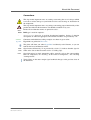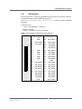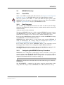
1
Embedded Solutions
20A012-00 E4 – 2012-12-03
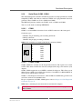
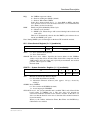
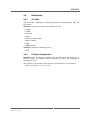
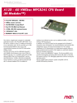
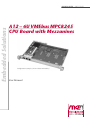
A12 – 6U VMEbus MPC8245
CPU Board with Mezzanines
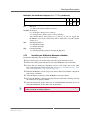
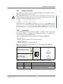
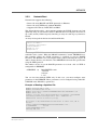
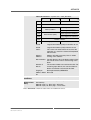
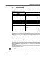
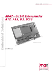
Configuration example (A12B without M-Modules)
User Manual
®
A12 – 6U VMEbus MPC8245 CPU Board with Mezzanines
A12 – 6U VMEbus MPC8245 CPU Board with Mezzanines
The A12B is a single-board computer for embedded applications based on the
PowerPC® MPC8245. It can be used as a master or slave in a VMEbus environment
or as a stand-alone card. The A12 provides up to 1 MB local shared SRAM for slave
access and communication between the local CPU and another VMEbus master.
The CPU card comes with the MPC8245 PowerPC® with 300 MHz clock
frequency and a local 32-bit/33-MHz PCI data bus. It is a complete state-of-the-art
SBC offering DRAM, Flash and CompactFlash® memory, dual Fast Ethernet, 4
COMs, USB, IDE and keyboard/mouse interfaces as well as an optional onboard
hard disk. A software-loadable FPGA is available with A12B for individual userdefined functions such as additional UARTs, a CAN bus interface, DSP functions
etc.
In addition, the A12 CPU board can be equipped with different mezzanine modules,
depending on the board variety. A12B cards support M-Modules™, which are
recommended for real-world I/O like analog/binary process I/O and instrumentation
I/O. A12A models can be equipped with PC-MIP® mezzanine cards for all types of
workstation I/O such as graphics, Ethernet or additional serial lines. A12C boards
offer two PMC sites. PMCs may particularly be used for intelligent telecom I/O.
The modular combination of I/O functionality on a single-board computer allows to
build up tailored control systems which appear as customized solutions based on
standard components.
The A12 comes with MENMON™ support. This firmware/BIOS can be used for
bootstrapping operating systems (from disk, flash or network), for hardware testing,
or for debugging applications without running any operating system.
The A12 single-board computer is partly compatible with the MVME2100 board by
Motorola.
MEN Mikro Elektronik GmbH
20A012-00 E4 – 2012-12-03
2
Technical Data
Technical Data
CPU
• PowerPC®
- MPC8245
- 300 MHz
- Double precision FPU
Memory
• L1 Cache integrated in MPC8245
• Up to 512 MB SDRAM system memory
- One 144-pin SO-DIMM slot for SDRAM modules
- 100 MHz memory bus frequency
• 2 MB Flash
• Serial EEPROM 2 KB for factory settings
• CompactFlash® card interface
- Via onboard IDE
- Type I
- True IDE
Mass Storage
• Parallel IDE (PATA)
- One port for local CompactFlash®
- One port for local hard-disk drive
- Drive can be connected via ribbon cable or mounted directly on the CPU
board using MEN adapter kit
- Only one VMEbus slot needed even with hard disk
I/O
• USB
- One USB 1.1 port
- Available via I/O connector
- External PHY
- Data rates up to 12 Mbit/s
• Ethernet
- Two 10/100Base-T Ethernet channels
- RJ45 connector at front panel with two LEDs
• One RS232 UART (COM1)
- RJ45 connector at front panel
- 16-byte transmit/receive buffer
- Handshake lines: CTS, RTS; DCD, DSR, DTR
MEN Mikro Elektronik GmbH
20A012-00 E4 – 2012-12-03
3
Technical Data
• One UART (COM2)
- Accessible via I/O connector
- Physical interface using SA-Adapter™ via 10-pin ribbon cable on I/O connector
- RS232..RS485, isolated or not: for free use in system (e.g., cable to front)
- 16-byte transmit/receive buffer
- Handshake lines: CTS, RTS; DCD, DSR, DTR; RI
• Two UARTs (COM3/COM4)
- Accessible via I/O connector
- Physical interface using SA-Adapter™ via 10-pin ribbon cable on I/O connector
- RS232..RS485, isolated or not: for free use in system (e.g., cable to front)
- Handshake lines: none
• PS/2 keyboard/mouse
- Accessible via I/O connector
- Requires external PHY
Mezzanine Extensions
• A12A: three PC-MIPs Type I/II on local PCI bus
- Compliant with PC-MIP specification
• A12B: Three M-Module™ slots
- Compliant with M-Module™ standard
- Characteristics: A08, A24, D16, D32, INTA, INTC
• A12C: Two PMC slots
- Compliant with PMC standard IEEE 1386.1
Miscellaneous
•
•
•
•
•
Serial real-time clock with integrated 56-byte NVRAM
Serial hardware watchdog in supervisory circuit
Temperature sensor
User LEDs (external)
Hex switch for user settings
Local PCI Bus
• 32-bit/33-MHz, 3.3V V(I/O)
• Compliant with PCI Specification 2.2
VMEbus
• Slot-1 function with auto-detection
• Master
- D08(EO):D16:A24:A16
- Transfer rate max. 7 MB/s
• Slave
- D08(EO):D16:A24:BLT
- Transfer rate max. 15 MB/s
• Up to 1 MB shared fast SRAM
• Interrupter D08(O):I(7-1):ROAK
• Interrupt handler D08(O):IH(7-1)
• Single level 3 fair requester
• Single level 3 arbiter
• Bus timer
MEN Mikro Elektronik GmbH
20A012-00 E4 – 2012-12-03
4
Technical Data
Electrical Specifications
• Supply voltage/power consumption:
- +5 V (-3%/+5%), 1.65 A typ.
- ±12 V (-5%/+5%), only used for mezzanines, tbd.
• MTBF: 63 000 h @ 50°C (derived from MIL-HDBK-217F)
Mechanical Specifications
• Dimensions: standard double Eurocard, 233.3 mm x 160 mm
• Weight (without mezzanines and accessories):
- A12A: 275g
- A12B: 273g
- A12C: 270g
Environmental Specifications
• Temperature range (operation):
- 0..+60°C or -40..+85°C (screened)
- Airflow: min. 10 m³/h
• Temperature range (storage): -40..+85°C
• Relative humidity (operation): max. 95% non-condensing
• Relative humidity (storage): max. 95% non-condensing
• Altitude: -300 m to +3000 m
• Shock: 15 g, 11 ms
• Bump: 10 g, 16 ms
• Vibration (sinusoidal): 2 g, 10..150 Hz
• Conformal coating on request
Safety
• PCB manufactured with a flammability rating of 94V-0 by UL recognized manufacturers
EMC
• Tested according to EN 55022 (radio disturbance), IEC1000-4-2 (ESD) and
IEC1000-4-4 (burst)
BIOS
• MENMON™
Software Support
•
•
•
•
•
Linux
VxWorks®
QNX®
OS-9®
For more information on supported operating system versions and drivers see
online data sheet.
MEN Mikro Elektronik GmbH
20A012-00 E4 – 2012-12-03
5
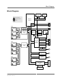
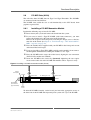
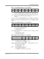
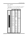
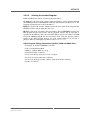
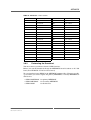
Block Diagram
Block Diagram
Boot/
Application Flash
SO‐DIMM
DRAM
F
Front connector
B
Onboard connector
64‐bit Data Bus
PowerPC®
MPC8245
Options
COM3
B
COM4
B
A12B
M‐Module™
FPGA User Function B
F
M‐Module™
PCI‐to‐
M‐Module™
Bridge
Temp. Sensor
Watchdog/
EEPROM
Compact‐
Flash
B
F
RTC
I²C
M‐Module™
F
IDE
PCI‐to‐ISA
Bridge
Super I/O
A12A
PC‐MIP®
PCI‐to‐PCI
Bridge
F
IDE
B
Mouse/Keyboard
B
USB
B
COM2
B
COM1
PC‐MIP®
F
RS232
F
F
10/100Base‐T
Ethernet
F
A12C
10/100Base‐T
Ethernet
F
PC‐MIP®
PMC
PMC
F
PCI‐to‐VME
Bridge
VMEbus P1
F
Ultra Fast SRAM
MEN Mikro Elektronik GmbH
20A012-00 E4 – 2012-12-03
6
Configuration Options
Configuration Options
CPU
• MPC8245, 300 MHz
Memory
• System RAM
- 64 MB, 128 MB, 256 MB or 512 MB
• CompactFlash®
- 0 MB up to maximum available
• Boot Flash
- 2 MB
SA-Adapters™
• Up to three SA-Adapters™ for UART functions (COM2..COM4)
• RS232, RS422, RS485
Operating Temperature
• 0..+60°C
• -40..+85°C
Please note that some of these options may only be available for large volumes.
Please ask our sales staff for more information.
For available standard configurations see online data sheet.
MEN Mikro Elektronik GmbH
20A012-00 E4 – 2012-12-03
7
Product Safety
Product Safety
!
Electrostatic Discharge (ESD)
Computer boards and components contain electrostatic sensitive devices.
Electrostatic discharge (ESD) can damage components. To protect the board and
other components against damage from static electricity, you should follow some
precautions whenever you work on your computer.
• Power down and unplug your computer system when working on the inside.
• Hold components by the edges and try not to touch the IC chips, leads, or circuitry.
• Use a grounded wrist strap before handling computer components.
• Place components on a grounded antistatic pad or on the bag that came with the
component whenever the components are separated from the system.
• Store the board only in its original ESD-protected packaging. Retain the original
packaging in case you need to return the board to MEN for repair.
MEN Mikro Elektronik GmbH
20A012-00 E4 – 2012-12-03
8
About this Document
About this Document
This user manual is intended only for system developers and integrators, it is not intended for end users.
It describes the hardware functions of the board, connection of peripheral devices
and integration into a system. It also provides additional information for special
applications and configurations of the board.
The manual does not include detailed information on individual components (data
sheets etc.). A list of literature is given in the appendix.
The A12 board was designed to support three types of mezzanines, in three
different basic varieties: A12A with PC-MIP modules, A12B with M-Modules,
and A12C with PMCs. This manual describes all of these three models and
generally refers to the board as "A12". However, since A12A and A12C models
are obsolete, product web links go to the A12B data sheet.
History
Issue
Date
E1
First edition
2001-12-17
E2
Second edition
2002-12-06
E3
Third edition
2004-01-30
E4
All product versions now delivered with DRAM
installed; general improvements
2012-12-03
MEN Mikro Elektronik GmbH
20A012-00 E4 – 2012-12-03
Comments
9
About this Document
Conventions
This sign marks important notes or warnings concerning the use of voltages which
can lead to serious damage to your health and also cause damage or destruction of
the component.
!
italics
bold
monospace
This sign marks important notes or warnings concerning proper functionality of the
product described in this document. You should read them in any case.
Folder, file and function names are printed in italics.
Bold type is used for emphasis.
A monospaced font type is used for hexadecimal numbers, listings, C function
descriptions or wherever appropriate. Hexadecimal numbers are preceded by "0x".
comment
Comments embedded into coding examples are shown in green color.
hyperlink
Hyperlinks are printed in blue color.
The globe will show you where hyperlinks lead directly to the Internet, so you can
look for the latest information online.
IRQ#
/IRQ
Signal names followed by "#" or preceded by a slash ("/") indicate that this signal is
either active low or that it becomes active at a falling edge.
in/out
Signal directions in signal mnemonics tables generally refer to the corresponding
board or component, "in" meaning "to the board or component", "out" meaning
"coming from it".
Vertical lines on the outer margin signal technical changes to the previous issue of
the document.
MEN Mikro Elektronik GmbH
20A012-00 E4 – 2012-12-03
10
About this Document
Legal Information
Changes
MEN Mikro Elektronik GmbH ("MEN") reserves the right to make changes without further notice to any products
herein.
Warranty, Guarantee, Liability
MEN makes no warranty, representation or guarantee of any kind regarding the suitability of its products for any
particular purpose, nor does MEN assume any liability arising out of the application or use of any product or
circuit, and specifically disclaims any and all liability, including, without limitation, consequential or incidental
damages. TO THE EXTENT APPLICABLE, SPECIFICALLY EXCLUDED ARE ANY IMPLIED
WARRANTIES ARISING BY OPERATION OF LAW, CUSTOM OR USAGE, INCLUDING WITHOUT
LIMITATION, THE IMPLIED WARRANTIES OF MERCHANTABILITY AND FITNESS FOR A
PARTICULAR PURPOSE OR USE. In no event shall MEN be liable for more than the contract price for the
products in question. If buyer does not notify MEN in writing within the foregoing warranty period, MEN shall
have no liability or obligation to buyer hereunder.
The publication is provided on the terms and understanding that:
1. MEN is not responsible for the results of any actions taken on the basis of information in the publication, nor
for any error in or omission from the publication; and
2. MEN is not engaged in rendering technical or other advice or services.
MEN expressly disclaims all and any liability and responsibility to any person, whether a reader of the publication
or not, in respect of anything, and of the consequences of anything, done or omitted to be done by any such person
in reliance, whether wholly or partially, on the whole or any part of the contents of the publication.
Conditions for Use, Field of Application
The correct function of MEN products in mission-critical and life-critical applications is limited to the
environmental specification given for each product in the technical user manual. The correct function of MEN
products under extended environmental conditions is limited to the individual requirement specification and
subsequent validation documents for each product for the applicable use case and has to be agreed upon in writing
by MEN and the customer. Should the customer purchase or use MEN products for any unintended or
unauthorized application, the customer shall indemnify and hold MEN and its officers, employees, subsidiaries,
affiliates, and distributors harmless against all claims, costs, damages, and expenses, and reasonable attorney fees
arising out of, directly or indirectly, any claim or personal injury or death associated with such unintended or
unauthorized use, even if such claim alleges that MEN was negligent regarding the design or manufacture of the
part. In no case is MEN liable for the correct function of the technical installation where MEN products are a part
of.
Trademarks
All products or services mentioned in this publication are identified by the trademarks, service marks, or product
names as designated by the companies which market those products. The trademarks and registered trademarks
are held by the companies producing them. Inquiries concerning such trademarks should be made directly to those
companies.
Conformity
MEN products are no ready-made products for end users. They are tested according to the standards given in the
Technical Data and thus enable you to achieve certification of the product according to the standards applicable in
your field of application.
MEN Mikro Elektronik GmbH
20A012-00 E4 – 2012-12-03
11
About this Document
RoHS
Since July 1, 2006 all MEN standard products comply with RoHS legislation.
Since January 2005 the SMD and manual soldering processes at MEN have already been completely lead-free.
Between June 2004 and June 30, 2006 MEN’s selected component suppliers have changed delivery to RoHScompliant parts. During this period any change and status was traceable through the MEN ERP system and the
boards gradually became RoHS-compliant.
WEEE Application
The WEEE directive does not apply to fixed industrial plants and tools. The compliance is the responsibility of the
company which puts the product on the market, as defined in the directive; components and sub-assemblies are
not subject to product compliance.
In other words: Since MEN does not deliver ready-made products to end users, the WEEE directive is not
applicable for MEN. Users are nevertheless recommended to properly recycle all electronic boards which have
passed their life cycle.
Nevertheless, MEN is registered as a manufacturer in Germany. The registration number can be provided on
request.
Copyright © 2012 MEN Mikro Elektronik GmbH. All rights reserved.
Germany
MEN Mikro Elektronik GmbH
Neuwieder Straße 3-7
90411 Nuremberg
Phone +49-911-99 33 5-0
Fax +49-911-99 33 5-901
E-mail [email protected]
www.men.de
MEN Mikro Elektronik GmbH
20A012-00 E4 – 2012-12-03
France
MEN Mikro Elektronik SA
18, rue René Cassin
ZA de la Châtelaine
74240 Gaillard
Phone +33 (0) 450-955-312
Fax +33 (0) 450-955-211
E-mail [email protected]
www.men-france.fr
USA
MEN Micro, Inc.
24 North Main Street
Ambler, PA 19002
Phone (215) 542-9575
Fax (215) 542-9577
E-mail [email protected]
www.menmicro.com
12
Contents
Contents
1 Getting Started . . . . . . . . . . . . . . . . . . . . . . . . . . . . . . . . . . . . . . . . . . . . . . . .
1.1 Maps of the Board . . . . . . . . . . . . . . . . . . . . . . . . . . . . . . . . . . . . . . . .
1.2 Configuring the Hardware . . . . . . . . . . . . . . . . . . . . . . . . . . . . . . . . . .
1.3 Integrating the Board into a System . . . . . . . . . . . . . . . . . . . . . . . . . .
1.4 Installing Operating System Software. . . . . . . . . . . . . . . . . . . . . . . . .
1.5 Installing Driver Software . . . . . . . . . . . . . . . . . . . . . . . . . . . . . . . . . .
18
18
22
23
24
24
2 Functional Description . . . . . . . . . . . . . . . . . . . . . . . . . . . . . . . . . . . . . . . . . .
2.1 Power Supply. . . . . . . . . . . . . . . . . . . . . . . . . . . . . . . . . . . . . . . . . . . .
2.2 Clock Supply . . . . . . . . . . . . . . . . . . . . . . . . . . . . . . . . . . . . . . . . . . . .
2.3 PowerPC CPU . . . . . . . . . . . . . . . . . . . . . . . . . . . . . . . . . . . . . . . . . . .
2.3.1
General . . . . . . . . . . . . . . . . . . . . . . . . . . . . . . . . . . . . . . . . .
2.3.2
Heat Sink. . . . . . . . . . . . . . . . . . . . . . . . . . . . . . . . . . . . . . . .
2.4 Bus Structure . . . . . . . . . . . . . . . . . . . . . . . . . . . . . . . . . . . . . . . . . . . .
2.4.1
Host-to-PCI Bridge . . . . . . . . . . . . . . . . . . . . . . . . . . . . . . . .
2.4.2
Local PCI Bus . . . . . . . . . . . . . . . . . . . . . . . . . . . . . . . . . . . .
2.4.3
PCI-to-ISA Bridge Super I/O Controller . . . . . . . . . . . . . . .
2.4.4
PCI-to-VMEbus Bridge . . . . . . . . . . . . . . . . . . . . . . . . . . . .
2.4.5
PCI-to-PCI Bridge. . . . . . . . . . . . . . . . . . . . . . . . . . . . . . . . .
2.5 Memory . . . . . . . . . . . . . . . . . . . . . . . . . . . . . . . . . . . . . . . . . . . . . . . .
2.5.1
SDRAM . . . . . . . . . . . . . . . . . . . . . . . . . . . . . . . . . . . . . . . .
2.5.2
Flash . . . . . . . . . . . . . . . . . . . . . . . . . . . . . . . . . . . . . . . . . . .
2.5.3
CompactFlash . . . . . . . . . . . . . . . . . . . . . . . . . . . . . . . . . . . .
2.5.4
EEPROM. . . . . . . . . . . . . . . . . . . . . . . . . . . . . . . . . . . . . . . .
2.6 PC-MIP Slots (A12A) . . . . . . . . . . . . . . . . . . . . . . . . . . . . . . . . . . . . .
2.6.1
Installing a PC-MIP Mezzanine Module . . . . . . . . . . . . . . .
2.6.2
PC-MIP Connectors . . . . . . . . . . . . . . . . . . . . . . . . . . . . . . .
2.7 M-Module Slots (A12B) . . . . . . . . . . . . . . . . . . . . . . . . . . . . . . . . . . .
2.7.1
Connection . . . . . . . . . . . . . . . . . . . . . . . . . . . . . . . . . . . . . .
2.7.2
Addressing the M-Modules. . . . . . . . . . . . . . . . . . . . . . . . . .
2.7.3
Installing an M-Module Mezzanine Module . . . . . . . . . . . .
2.8 PMC Slots (A12C) . . . . . . . . . . . . . . . . . . . . . . . . . . . . . . . . . . . . . . .
2.8.1
Installing a PMC Mezzanine Module . . . . . . . . . . . . . . . . . .
2.9 IDE Interface . . . . . . . . . . . . . . . . . . . . . . . . . . . . . . . . . . . . . . . . . . . .
2.9.1
Fuse Protection . . . . . . . . . . . . . . . . . . . . . . . . . . . . . . . . . . .
2.9.2
Installing a Hard Disk . . . . . . . . . . . . . . . . . . . . . . . . . . . . . .
2.10 Ethernet Interface . . . . . . . . . . . . . . . . . . . . . . . . . . . . . . . . . . . . . . . .
2.10.1 Connection . . . . . . . . . . . . . . . . . . . . . . . . . . . . . . . . . . . . . .
2.11 I/O Expansion Connector . . . . . . . . . . . . . . . . . . . . . . . . . . . . . . . . . .
2.11.1 Fuse Protection . . . . . . . . . . . . . . . . . . . . . . . . . . . . . . . . . . .
2.12 Serial Ports COM1..COM4 . . . . . . . . . . . . . . . . . . . . . . . . . . . . . . . . .
2.12.1 COM1 . . . . . . . . . . . . . . . . . . . . . . . . . . . . . . . . . . . . . . . . . .
2.12.2 COM2..COM4 . . . . . . . . . . . . . . . . . . . . . . . . . . . . . . . . . . .
25
25
25
25
25
25
26
26
26
26
26
26
27
27
28
28
29
30
30
31
32
32
33
34
36
36
38
39
40
42
42
43
45
46
46
46
MEN Mikro Elektronik GmbH
20A012-00 E4 – 2012-12-03
13
Contents
2.13
2.14
2.15
2.16
2.17
Temperature Sensor . . . . . . . . . . . . . . . . . . . . . . . . . . . . . . . . . . . . . . .
Real-Time Clock and NVRAM . . . . . . . . . . . . . . . . . . . . . . . . . . . . . .
Watchdog . . . . . . . . . . . . . . . . . . . . . . . . . . . . . . . . . . . . . . . . . . . . . . .
User-Defined Hex Switch . . . . . . . . . . . . . . . . . . . . . . . . . . . . . . . . . .
VMEbus Interface . . . . . . . . . . . . . . . . . . . . . . . . . . . . . . . . . . . . . . . .
2.17.1 SRAM . . . . . . . . . . . . . . . . . . . . . . . . . . . . . . . . . . . . . . . . . .
2.17.2 Slot-1 Function . . . . . . . . . . . . . . . . . . . . . . . . . . . . . . . . . . .
2.17.3 Interrupter . . . . . . . . . . . . . . . . . . . . . . . . . . . . . . . . . . . . . . .
2.17.4 Interrupt Handler. . . . . . . . . . . . . . . . . . . . . . . . . . . . . . . . . .
2.17.5 Bus Errors . . . . . . . . . . . . . . . . . . . . . . . . . . . . . . . . . . . . . . .
2.17.6 Master Access . . . . . . . . . . . . . . . . . . . . . . . . . . . . . . . . . . . .
2.17.7 Atomic Operations . . . . . . . . . . . . . . . . . . . . . . . . . . . . . . . .
2.17.8 PCI Configuration Space Registers. . . . . . . . . . . . . . . . . . . .
2.17.9 Runtime Registers . . . . . . . . . . . . . . . . . . . . . . . . . . . . . . . . .
2.17.10 Connection . . . . . . . . . . . . . . . . . . . . . . . . . . . . . . . . . . . . . .
48
48
48
48
49
49
49
49
50
50
50
50
51
52
55
3 MENMON . . . . . . . . . . . . . . . . . . . . . . . . . . . . . . . . . . . . . . . . . . . . . . . . . . . .
3.1 General . . . . . . . . . . . . . . . . . . . . . . . . . . . . . . . . . . . . . . . . . . . . . . . .
3.2 Console . . . . . . . . . . . . . . . . . . . . . . . . . . . . . . . . . . . . . . . . . . . . . . . .
3.3 MENMON Memory Map . . . . . . . . . . . . . . . . . . . . . . . . . . . . . . . . . .
3.4 MENMON Start-up . . . . . . . . . . . . . . . . . . . . . . . . . . . . . . . . . . . . . . .
3.4.1
User LEDs. . . . . . . . . . . . . . . . . . . . . . . . . . . . . . . . . . . . . . .
3.4.2
Boot Sequence. . . . . . . . . . . . . . . . . . . . . . . . . . . . . . . . . . . .
3.4.3
Configuring the MENMON Start-up Procedure . . . . . . . . . .
3.4.4
Self Tests . . . . . . . . . . . . . . . . . . . . . . . . . . . . . . . . . . . . . . . .
3.5 MENMON Boot Methods for Client Programs . . . . . . . . . . . . . . . . .
3.5.1
MENMON BIOS Devices. . . . . . . . . . . . . . . . . . . . . . . . . . .
3.5.2
Disk Boot . . . . . . . . . . . . . . . . . . . . . . . . . . . . . . . . . . . . . . .
3.5.3
Network Boot . . . . . . . . . . . . . . . . . . . . . . . . . . . . . . . . . . . .
3.6 Updating Flash Devices. . . . . . . . . . . . . . . . . . . . . . . . . . . . . . . . . . . .
3.6.1
Download via Serial Interface. . . . . . . . . . . . . . . . . . . . . . . .
3.6.2
Performing the Download . . . . . . . . . . . . . . . . . . . . . . . . . . .
3.6.3
Update from Disk or Network. . . . . . . . . . . . . . . . . . . . . . . .
3.7 MENMON User Interface . . . . . . . . . . . . . . . . . . . . . . . . . . . . . . . . . .
3.7.1
Command Line Editing . . . . . . . . . . . . . . . . . . . . . . . . . . . . .
3.7.2
Numerical Arguments . . . . . . . . . . . . . . . . . . . . . . . . . . . . . .
3.7.3
MENMON Command Overview . . . . . . . . . . . . . . . . . . . . .
3.8 Board Setup . . . . . . . . . . . . . . . . . . . . . . . . . . . . . . . . . . . . . . . . . . . . .
3.8.1
ALI 1543 . . . . . . . . . . . . . . . . . . . . . . . . . . . . . . . . . . . . . . . .
3.8.2
PCI Auto-Configuration . . . . . . . . . . . . . . . . . . . . . . . . . . . .
3.8.3
SDRAM DIMM Configuration. . . . . . . . . . . . . . . . . . . . . . .
3.8.4
VMEbus Configuration . . . . . . . . . . . . . . . . . . . . . . . . . . . . .
3.8.5
Watchdog Configuration . . . . . . . . . . . . . . . . . . . . . . . . . . . .
3.8.6
Hex Switch . . . . . . . . . . . . . . . . . . . . . . . . . . . . . . . . . . . . . .
56
56
56
57
58
58
58
58
59
61
61
63
70
72
72
73
74
75
75
75
76
78
78
78
80
80
81
81
MEN Mikro Elektronik GmbH
20A012-00 E4 – 2012-12-03
14
Contents
3.9 MENMON System Calls . . . . . . . . . . . . . . . . . . . . . . . . . . . . . . . . . . .
3.9.1
Invoking System Calls. . . . . . . . . . . . . . . . . . . . . . . . . . . . . .
3.9.2
System Calls . . . . . . . . . . . . . . . . . . . . . . . . . . . . . . . . . . . . .
3.10 VxWorks Bootline . . . . . . . . . . . . . . . . . . . . . . . . . . . . . . . . . . . . . . . .
3.10.1 Additional MENMON Parameters . . . . . . . . . . . . . . . . . . . .
82
82
83
87
89
4 Organization of the Board . . . . . . . . . . . . . . . . . . . . . . . . . . . . . . . . . . . . . . .
4.1 Memory Mappings . . . . . . . . . . . . . . . . . . . . . . . . . . . . . . . . . . . . . . .
4.1.1
Processor View of the Memory Map. . . . . . . . . . . . . . . . . . .
4.1.2
PCI/ISA I/O Space Memory Map . . . . . . . . . . . . . . . . . . . . .
4.1.3
VMEbus Memory Mapping . . . . . . . . . . . . . . . . . . . . . . . . .
4.2 Interrupt Handling . . . . . . . . . . . . . . . . . . . . . . . . . . . . . . . . . . . . . . . .
4.2.1
Nonmaskable Interrupts . . . . . . . . . . . . . . . . . . . . . . . . . . . .
4.2.2
Maskable Interrupts. . . . . . . . . . . . . . . . . . . . . . . . . . . . . . . .
4.3 Implementation of M1543 PCI-to-ISA Bridge . . . . . . . . . . . . . . . . . .
4.4 SMB Devices . . . . . . . . . . . . . . . . . . . . . . . . . . . . . . . . . . . . . . . . . . . .
4.5 PCI Devices on Bus 0 . . . . . . . . . . . . . . . . . . . . . . . . . . . . . . . . . . . . .
4.6 PCI Devices on PC-MIP/PMC Bus . . . . . . . . . . . . . . . . . . . . . . . . . . .
4.7 M-Module Interface. . . . . . . . . . . . . . . . . . . . . . . . . . . . . . . . . . . . . . .
90
90
90
92
93
94
94
94
95
96
96
97
97
5 Appendix . . . . . . . . . . . . . . . . . . . . . . . . . . . . . . . . . . . . . . . . . . . . . . . . . . . . . 98
5.1 Literature and Web Resources . . . . . . . . . . . . . . . . . . . . . . . . . . . . . . . 98
5.1.1
PowerPC . . . . . . . . . . . . . . . . . . . . . . . . . . . . . . . . . . . . . . . . 98
5.1.2
VMEbus . . . . . . . . . . . . . . . . . . . . . . . . . . . . . . . . . . . . . . . . 98
5.1.3
PCI . . . . . . . . . . . . . . . . . . . . . . . . . . . . . . . . . . . . . . . . . . . . 98
5.1.4
Bridges . . . . . . . . . . . . . . . . . . . . . . . . . . . . . . . . . . . . . . . . . 98
5.1.5
PC-MIP . . . . . . . . . . . . . . . . . . . . . . . . . . . . . . . . . . . . . . . . . 98
5.1.6
M-Modules . . . . . . . . . . . . . . . . . . . . . . . . . . . . . . . . . . . . . . 98
5.1.7
PMC . . . . . . . . . . . . . . . . . . . . . . . . . . . . . . . . . . . . . . . . . . . 99
5.1.8
Ethernet . . . . . . . . . . . . . . . . . . . . . . . . . . . . . . . . . . . . . . . . . 99
5.1.9
EIDE . . . . . . . . . . . . . . . . . . . . . . . . . . . . . . . . . . . . . . . . . . . 99
5.1.10 USB . . . . . . . . . . . . . . . . . . . . . . . . . . . . . . . . . . . . . . . . . . . . 99
5.2 Finding out the Board’s Article Number, Revision and Serial
Number . . . . . . . . . . . . . . . . . . . . . . . . . . . . . . . . . . . . . . . . . . . . . . . 100
MEN Mikro Elektronik GmbH
20A012-00 E4 – 2012-12-03
15
Figures
Figure 1. General board map – top view . . . . . . . . . . . . . . . . . . . . . . . . . . . . . . . 18
Figure 2. A12A board map – CPU board with PC-MIPs – top view. . . . . . . . . . 19
Figure 3. A12B board map – CPU board with M-Modules – top view. . . . . . . . 20
Figure 4. A12C board map – CPU board with PMCs – top view . . . . . . . . . . . . 21
Figure 5. SO-DIMM DRAM installation. . . . . . . . . . . . . . . . . . . . . . . . . . . . . . . 27
Figure 6. Installing a PC-MIP mezzanine module (A12A) . . . . . . . . . . . . . . . . . 30
Figure 7. Installing an M-Module mezzanine module (A12B) . . . . . . . . . . . . . . 35
Figure 8. Installing a PMC mezzanine module (A12C). . . . . . . . . . . . . . . . . . . . 37
Figure 9. Position of fuse for IDE power supply protection . . . . . . . . . . . . . . . . 39
Figure 10. A12C with hard-disk adapter and hard disk . . . . . . . . . . . . . . . . . . . . . 40
Figure 11. Position of hard-disk adapter card on the board . . . . . . . . . . . . . . . . . . 41
Figure 12. Position of fuse for I/O connector protection . . . . . . . . . . . . . . . . . . . . 45
Figure 13. Position of hex switch. . . . . . . . . . . . . . . . . . . . . . . . . . . . . . . . . . . . . . 48
Figure 14. MENMON – Address mapping . . . . . . . . . . . . . . . . . . . . . . . . . . . . . . 57
Figure 15. MENMON – Layout of the 0x41-type partition (PReP) . . . . . . . . . . 63
Figure 16. MENMON – Example PCI configuration . . . . . . . . . . . . . . . . . . . . . . 79
Figure 17. Labels giving the product’s article number, revision and serial
number . . . . . . . . . . . . . . . . . . . . . . . . . . . . . . . . . . . . . . . . . . . . . . . . 100
MEN Mikro Elektronik GmbH
20A012-00 E4 – 2012-12-03
16
Tables
Table 1.
Table 2.
Table 3.
Table 4.
Table 5.
Table 6.
Table 7.
Table 8.
Table 9.
Table 10.
Table 11.
Table 12.
Table 13.
Table 14.
Table 15.
Table 16.
Table 17.
Table 18.
Table 19.
Table 20.
Table 21.
Table 22.
Table 23.
Table 24.
Table 25.
Table 26.
Table 27.
Table 28.
Table 29.
Table 30.
Table 31.
Table 32.
Table 33.
Table 34.
Table 35.
MEN Mikro Elektronik GmbH
20A012-00 E4 – 2012-12-03
Pin assignment of the 60-pin M-Module plug connectors . . . . . . . . . . 32
M-Module address map . . . . . . . . . . . . . . . . . . . . . . . . . . . . . . . . . . . . 33
Pin assignment of the 44-pin IDE connector . . . . . . . . . . . . . . . . . . . . 38
Signal mnemonics for the IDE connector. . . . . . . . . . . . . . . . . . . . . . . 39
Pin assignment and status LEDs of the 8-pin RJ45 Ethernet 10Base-T/
100Base-T connectors . . . . . . . . . . . . . . . . . . . . . . . . . . . . . . . . . . . . . 42
Signal mnemonics of the Ethernet 10Base-T/100Base-T connectors . 42
Pin assignment of the 40-pin I/O expansion connector . . . . . . . . . . . . 43
Signal mnemonics of 40-pin I/O expansion connector . . . . . . . . . . . . 44
Pin assignment of 8-pin RJ45 RS232 connector (COM1) . . . . . . . . . . 46
PCI Configuration Space Registers . . . . . . . . . . . . . . . . . . . . . . . . . . . 51
Pin assignment of 3-row, 96-pin VMEbus connector P1 . . . . . . . . . . . 55
MENMON – Assignment of board controller devices. . . . . . . . . . . . . 62
MENMON – Download destination devices . . . . . . . . . . . . . . . . . . . . 72
MENMON – Flash sectors . . . . . . . . . . . . . . . . . . . . . . . . . . . . . . . . . . 73
MENMON – Command overview . . . . . . . . . . . . . . . . . . . . . . . . . . . . 76
Hex-switch settings. . . . . . . . . . . . . . . . . . . . . . . . . . . . . . . . . . . . . . . . 81
MENMON – System calls – BRD_ID fields . . . . . . . . . . . . . . . . . . . . 83
MENMON – System calls – RTC_RD buffer data . . . . . . . . . . . . . . . 85
MENMON – System calls – DSK_RD fields . . . . . . . . . . . . . . . . . . . 86
MENMON – VxWorks bootline – List of parameters and their usage 88
MENMON – Common parameters passed by all MENMONs . . . . . . 89
Memory map – processor view . . . . . . . . . . . . . . . . . . . . . . . . . . . . . . 90
Address mapping for PCI . . . . . . . . . . . . . . . . . . . . . . . . . . . . . . . . . . . 90
BATS set up by MENMON . . . . . . . . . . . . . . . . . . . . . . . . . . . . . . . . . 91
PCI/ISA I/O space memory map (addresses as seen from CPU) . . . . . 92
VMEbus memory mapping . . . . . . . . . . . . . . . . . . . . . . . . . . . . . . . . . 93
Interrupts on the CPU board. . . . . . . . . . . . . . . . . . . . . . . . . . . . . . . . . 94
M1543 General Purpose Input (GPI) pin assignments. . . . . . . . . . . . . 95
M1543 General Purpose Output (GPO) pin assignments. . . . . . . . . . . 95
M1543 General Purpose Input/Output (GPIO) pin assignments . . . . . 95
SMB 1 devices . . . . . . . . . . . . . . . . . . . . . . . . . . . . . . . . . . . . . . . . . . . 96
SMB 2 devices . . . . . . . . . . . . . . . . . . . . . . . . . . . . . . . . . . . . . . . . . . . 96
PCI devices on Bus 0 . . . . . . . . . . . . . . . . . . . . . . . . . . . . . . . . . . . . . . 96
PCI devices on PC-MIP/PMC bus . . . . . . . . . . . . . . . . . . . . . . . . . . . . 97
M-Module device addresses . . . . . . . . . . . . . . . . . . . . . . . . . . . . . . . . . 97
17
Getting Started
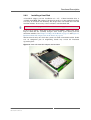
1
Getting Started
This chapter will give an overview of the board and some hints for first installation
in a system as a "check list".
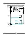
1.1
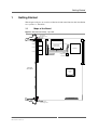
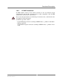
Maps of the Board
Figure 1. General board map – top view
Front‐panel mounting screw
CompactFlash
card connector
MPC8245
1
VMEbus P1
LAN 1
CompactFlash
metal holder
I/O Connector
Reset Button/LED
RS232 COM1
SO‐DIMM
DRAM Socket
LAN 2
Production/Test
User‐
configurable hex switch
Front Panel
Side of Board
M1543
ALI
IDE Interface
Front‐panel mounting screw
MEN Mikro Elektronik GmbH
20A012-00 E4 – 2012-12-03
18
Getting Started
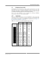
Figure 2. A12A board map – CPU board with PC-MIPs – top view
Front‐panel mounting screw
CompactFlash
metal holder
MPC8245
VMEbus P1
LAN 1
CompactFlash
card connector
1
I/O Connector
Reset Button/LED
RS232 COM1
SO‐DIMM
DRAM Socket
LAN 2
Production/Test
User‐
configurable hex switch
PC‐MIP 2
Front Panel
Side of Board
M1543
ALI
PC‐MIP bezel keepers
PC‐MIP 1
PC‐MIP
keeper screw (solder side)
Finished bezel
of PC‐MIP I/O connector
PC‐MIP 0
IDE Interface
Front‐panel mounting screw Injectors/ejectors with threaded standoffs and captive screws
MEN Mikro Elektronik GmbH
20A012-00 E4 – 2012-12-03
19
Getting Started
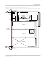
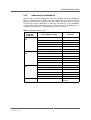
Figure 3. A12B board map – CPU board with M-Modules – top view
Front‐panel mounting screw
CompactFlash
metal holder
I/O Connector
LAN 1
CompactFlash
card connector
MPC8245
1
VMEbus P1
Reset Button/LED
RS232 COM1
SO‐DIMM
DRAM Socket
LAN 2
User‐
configurable hex switch
60‐pin plug connector
Production/Test
M‐Module 2
M1543
ALI
Holes for M‐Module Mounting Screws
60‐pin plug connector
M‐Module 1
60‐pin plug connector
Front Panel
Side of Board
M‐Module 0
IDE Interface
Front‐panel mounting screw
MEN Mikro Elektronik GmbH
20A012-00 E4 – 2012-12-03
20
Getting Started
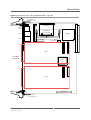
Figure 4. A12C board map – CPU board with PMCs – top view
Front‐panel mounting screw
CompactFlash
metal holder
I/O Connector
LAN 1
CompactFlash
card connector
MPC8245
1
VMEbus P1
Reset Button/LED
RS232 COM1
SO‐DIMM
DRAM Socket
LAN 2
User‐
configurable hex switch
Production/Test
PMC 1
Front Panel
Side of Board
M1543
ALI
PMC 0
IDE Interface
Front‐panel mounting screw
MEN Mikro Elektronik GmbH
20A012-00 E4 – 2012-12-03
21
Getting Started
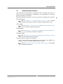
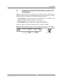
1.2
Configuring the Hardware
You should check your hardware requirements before installing the board in a
system, since most modifications are difficult or even impossible to do when the
board is mounted in an enclosure.
The following check list will give an overview on what you might want to configure.
CompactFlash
Refer to Chapter 2.5.3 CompactFlash on page 28 for a detailed
installation description and hints on supported CompactFlash cards.
PC-MIPs
Refer to Chapter 2.6.1 Installing a PC-MIP Mezzanine Module on page
30 for a detailed installation description.
M-Modules
Refer to Chapter 2.7.3 Installing an M-Module Mezzanine Module on
page 34 for a detailed installation description.
PMC modules
Refer to Chapter 2.8.1 Installing a PMC Mezzanine Module on page 36
for a detailed installation description.
Serial interface adapters (SA-Adapters)
You can install standard serial interfaces such as RS232 using MEN’s SAAdapters on the A12’s COM2..COM4 UART connectors.
Refer to Chapter 2.12 Serial Ports COM1..COM4 on page 46 for detailed
installation descriptions.
MEN Mikro Elektronik GmbH
20A012-00 E4 – 2012-12-03
22
Getting Started
1.3
Integrating the Board into a System
The A12 is a complex board and setting it up requires experience. You can use the
following check list when installing the CPU board in a system for the first time and
with minimum configuration.
!
The board is completely trimmed on delivery. Perform the following procedure
without any mezzanine module installed!
Power-down the system.
Remove all boards from the VMEbus system.
Insert the A12 into slot 1 of the system, making sure that the connectors are
properly aligned.
Connect a terminal to the standard RS232 interface COM1 (RJ45 connector).
Set your terminal to the following protocol:
-
9600 baud data transmission rate
8 data bits
1 stop bit
No parity
Power-up the system.
The terminal displays a message similar to the following:
_________________ Secondary MenMon for the A012/D003 Version 2.0 ____________
|
|
|
(c) 1999 - 2001 MEN mikro elektronik GmbH Nuernberg
|
|
Parts of this code based on Motorola's Dink32
|
|
Created Jul 11 2001
15:24:33
|
|_____________________________________________________________________________|
|
HW Revision: 01.00.00
|
CPU: MPC8245
(MAP B)
|
| Serial Number: 44
| CPU/MEM Clock: 300 / 100 MHz
|
|
Board Model: A012b00
|
DIMM Module: 64 MB Setup: 222
|
\___________________________________________________________________________/
Init VME controller (FPGA rev. 2, VME slot1 function enabled)
press 'ESC' to setup/MENMON
Selftest running ...
CHECKSUM
==> OK
*** Can't jump to bootstrapper. BS address in EEPROM invalid!
MenMon>
Now you can use the MENMON debugger (see detailed description in Chapter
3 MENMON on page 56).
Observe the installation instructions for the respective software.
MEN Mikro Elektronik GmbH
20A012-00 E4 – 2012-12-03
23
Getting Started
1.4
Installing Operating System Software
The board supports VxWorks, Linux, OS-9 and QNX.
!
By default, no operating system is installed on the board. Please refer to the
respective manufacturer's documentation on how to configure your operating
system image!
You can find any software available in the A12B pages on MEN’s website.
1.5
Installing Driver Software
For a detailed description on how to install driver software please refer to the
respective documentation.
MEN Mikro Elektronik GmbH
20A012-00 E4 – 2012-12-03
24
Functional Description
2
Functional Description
The following describes the individual functions of the board and their
configuration on the board. There is no detailed description of the individual
controller chips and the CPUs. They can be obtained from the data sheets or data
books of the semiconductor manufacturer concerned (Chapter 5.1 Literature and
Web Resources on page 98).
Please note that the board BSPs for the different operating systems may not support all the functions of the A12. For more information on hardware support please
see the respective BSP data sheet on MEN’s website: A12B pages
2.1
Power Supply
The board is supplied with +5 V and ±12 V via the VMEbus. However, ±12 V may
be required only by some mezzanine modules.
The onboard power supply generates the 2.0 V core voltage and 3.3 V I/O voltage of
the PowerPC.
2.2
Clock Supply
The clock supply generates all clocks for the onboard devices (PowerPC, SDRAM,
host bridge, PCI bus devices). The clock frequency is factory-set.
The local PCI clock operates at 33 MHz.
2.3
PowerPC CPU
The board is equipped with the MPC8245 Kahlua II processor, which includes a 32bit superscalar PowerPC 603e core, the integrated host-to-PCI bridge, and two
UARTs.
2.3.1
General
The PowerPC architecture, developed jointly by Motorola, IBM, and Apple
Computer, is based on the POWER architecture implemented by the RS/6000™
family of computers. The PowerPC architecture takes advantage of recent
technological advances in such areas as process technology, compiler design, and
RISC microprocessor design to provide software compatibility across a diverse
family of implementations, primarily single-chip microprocessors, intended for a
wide range of systems.
2.3.2
Heat Sink
A heat sink is provided to meet thermal requirements.
MEN Mikro Elektronik GmbH
20A012-00 E4 – 2012-12-03
25
Functional Description
2.4
Bus Structure
2.4.1
Host-to-PCI Bridge
The integrated host-to-PCI bridge (internal in MPC8245) is used as host bridge and
memory controller for the PowerPC processor. All transactions of the PowerPC to
the PCI bus are controlled by the host bridge. The SDRAM and boot Flash are
connected to the local memory bus of the integrated host-to-PCI bridge.
The PCI interface is PCI bus Rev. 2.2 compliant and supports all bus commands and
transactions. Master and target operations are possible. Only big-endian operation is
supported.
2.4.2
Local PCI Bus
The local PCI bus is controlled by the integrated host-to-PCI bridge. It runs at
33 MHz. The I/O voltage is fixed to 3.3 V. The data width is 32 bits.
Major functional elements of the board, such as Ethernet, are connected to the local
PCI bus.
2.4.3
PCI-to-ISA Bridge Super I/O Controller
The M1543 provides integrated Super I/O (2 serial ports), system peripherals (ISP)
(2 82C59 and serial interrupt, 1 82C54), advanced features (type F and distributed
DMA) in the DMA controller (2 82C37), PS2 keyboard/mouse controller, 2-channel
dedicated IDE master controller with Ultra-33 specification and System
Management Bus (SMB).
M1543 also provides a PCI-to-ISA IRQ routing table, and level-to-edge trigger
transfer.
2.4.4
PCI-to-VMEbus Bridge
The board has a PCI-to-VME bridge for connection to the VMEbus. It is
implemented in an FPGA. On the local PCI bus this bridge is a target. The local
processor can thus freely access the VMEbus (master). For communication in
multiprocess applications, the bridge has a fast communication memory of up to
1MB size. This memory can be accessed both from the local processor and from the
VMEbus (slave).
2.4.5
PCI-to-PCI Bridge
The A12A and A12C boards have a secondary PCI bus for accesses to PC-MIP and
PMC modules. It is controlled by a PCI-to-PCI bridge of type 2031 from TI.
MEN Mikro Elektronik GmbH
20A012-00 E4 – 2012-12-03
26
Functional Description
2.5
Memory
2.5.1
SDRAM
One SDRAM bank (bank 0) is implemented on the board. Bank 0 is connected to a
144-pin SO-DIMM connector. The current board version supports SO-DIMMs up to
512 MB.
The board is shipped with a tested DRAM SO-DIMM module installed. If for any
reason you need to exchange or install an SO-DIMM module, please stick to the
following procedure.
Note: MEN gives no warranty on functionality and reliability of the board if you
use any other module than that qualified and/or supplied by MEN. Please
contact either MEN directly or your local MEN sales office.
Figure 5. SO-DIMM DRAM installation
SO‐DIMM Memory Module
Safety Notch
Clip
Contact Groove
Clip
Safety Tab
SO‐DIMM Socket
The DRAM module will only fit as shown above because of a safety tab on the SODIMM socket which requires a notch in the SO-DIMM module.
!
Power down the system before installing a SO-DIMM module to avoid damage
of the board!
Place the memory module into the socket at a 45° angle and make sure that the
safety tab and notch are aligned.
Carefully push the memory module into the contact groove of the socket.
Press the memory module down until it clicks into place.
The clips of the socket now hold the memory module in place.
To release the module, squeeze both clips outwards and carefully pull the module out of the socket.
MEN Mikro Elektronik GmbH
20A012-00 E4 – 2012-12-03
27
Functional Description
2.5.2
!
Flash
The board has onboard Flash. It is controlled by the integrated host-to-PCI bridge of
the MPC8245 and can accommodate 2 MB. The data bus is 8 bits wide.
Flash memory contains the boot software for the MENMON/operating system
bootstrapper and application software. The MENMON sectors are softwareprotected against illegal write transactions through a password in the serial
download function of MENMON (cf. Chapter 3.6 Updating Flash Devices on page
72).
2.5.3
CompactFlash
CompactFlash is a standard for small form factor ATA Flash drives. It is electrically
compatible to the PC Card 1995 and PC Card ATA standards.
The CompactFlash standard is supported by industry’s leading vendors of Flash
cards and others.
CompactFlash cards are operated in a True IDE Mode.
2.5.3.1
Installing a CompactFlash Card
The CompactFlash slot is within the SO-DIMM DRAM socket, i.e. the
CompactFlash card is placed below a DRAM module.
The board is shipped without a CompactFlash card installed. To install
CompactFlash, please stick to the following procedure.
Power down your system and remove the board from the system.
Remove the SO-DIMM module installed in the DRAM socket as described in
Chapter 2.5.1 SDRAM on page 27.
Remove the metal holder that is included with the board to secure the CompactFlash card. To do this, loosen and remove the two cross-recess screws from the
bottom side of the PCB.
Front‐panel mounting screw
LAN 1
CompactFlash
metal holder
CompactFlash
card connector
MPC8245
1
I/O Connector
Reset Button/LED
RS232 COM1
Remove screws from
bottom side of PCB
SO‐DIMM
DRAM Socket
LAN 2
Production/Test
MEN Mikro Elektronik GmbH
20A012-00 E4 – 2012-12-03
User‐
configurable hex switch
28
Functional Description
Insert the CompactFlash card carefully as indicated by the arrow on top of the
card, making sure that all the contacts are aligned properly and the card is
firmly connected with the card connector.
Front‐panel mounting screw
LAN 1
CompactFlash
Card
CompactFlash
metal holder
I/O Connector
Reset Button/LED
RS232 COM1
Insert the
CompactFlash card
CompactFlash
card connector
MPC8245
1
SO‐DIMM
DRAM Socket
LAN 2
Production/Test
User‐
configurable hex switch
Reinstall the metal holder: Place the holder over the CompactFlash card and
carefully align the screw holes of the holder and the board. Make sure to
include the nut between each screw and the PCB.
Reinstall your SO-DIMM module.
To remove the CompactFlash card you must again remove and then reinstall the
SO-DIMM module and metal holder as described above.
Observe manufacturer notes on usage of CompactFlash cards.
2.5.3.2
Supported CompactFlash Cards
The board supports standard CompactFlash cards.
You can order suitable CompactFlash cards from MEN. Please see the A12B
pages on MEN’s website for ordering options.
2.5.4
EEPROM
The board has a 2-Kbyte serial EEPROM for factory data, MENMON parameters,
and for the VxWorks bootline.
MEN Mikro Elektronik GmbH
20A012-00 E4 – 2012-12-03
29
Functional Description
2.6
PC-MIP Slots (A12A)
The A12A has three PC-MIP slots for Type-I and Type-II modules. The PC-MIPs
are connected to the local PCI bus.
The PC-MIP slots enable the user to add functionality to the CPU board, from
graphics to process I/O.
2.6.1
Installing a PC-MIP Mezzanine Module
Perform the following steps to install a PC-MIP:
Power down your system and remove the board from the system.
If you want to install a Type-II PC-MIP (with front connector), you must
remove the blank bezel at the front panel of the board first:
Remove the respective bezel keeper by loosening the keeper screw at the bottom side of the board. (See Figure 2, A12A board map – CPU board with PCMIPs – top view, on page 19).
Place the finished bezel supplied with your PC-MIP in the front panel cut-out
and reinstall the bezel keeper.
If you are installing a Type-II PC-MIP, carefully put the module’s front connector through the finished bezel, holding the module at a 45° angle.
Place the PC-MIP on the target slot of the board, aligning the two connectors
(P1/J1, P2/J2) and the two standoffs.
Screw the PC-MIP to the carrier by alternately tightening the two captive
screws on the label side of the PC-MIP. The module will be "injected" safely.
Figure 6. Installing a PC-MIP mezzanine module (A12A)
System
front panel
Keeper
Captive screw
J3
P3
PC‐MIP front
I/O connector
(Type II module)
PC‐MIP (Type I or II)
J1
P1
Standoff
Captive screw
Standoff
CPU board
Keeper screw
To deinstall PC-MIPs from the carrier board, just loosen the appropriate screws at
the label side of the PC-MIP. The injector/ejector system will "eject" the PC-MIP.
MEN Mikro Elektronik GmbH
20A012-00 E4 – 2012-12-03
30
Functional Description
2.6.2
PC-MIP Connectors
PC-MIP modules connect to the board’s PCI bus via the two identical 64-pin
connectors P1 and P2. The connector layout is fully compatible to the PC-MIP
specification and will not be repeated here.
!
Please note that the board has no third 64-pin connectors (P3), and therefore does
not support rear I/O connection.
Connector types of P1 and P2:
• 64-pin SMT plug connector according to IEEE P1386, e. g. Molex 71436-0864
• Mating connector:
64-pin SMT receptacle connector according to IEEE P1386, e. g. Molex 714391864
MEN Mikro Elektronik GmbH
20A012-00 E4 – 2012-12-03
31
Functional Description
2.7
M-Module Slots (A12B)
The M-Module slots enable the user to add a number of I/O functions to the CPU
board. The wide range of standardized M-Modules includes not only process I/O
modules but also interface extensions, network boards (such as Profibus, CAN bus
etc.), DSP and transputer modules and special-purpose functions.
The A12 has three M-Module slots and supports the following M-Module
characteristics: D16, D32, A08, A24, INTA, INTC.
2.7.1
Connection
The signals from the CPU board are fed to the M-Module via three 20-pin plug
connector rows. These connectors correspond to connectors on the M-Module. The
pin assignment corresponds to the M-Module specification (see Chapter 5.1
Literature and Web Resources on page 98).
Table 1. Pin assignment of the 60-pin M-Module plug connectors
A
1
20
MEN Mikro Elektronik GmbH
20A012-00 E4 – 2012-12-03
B
C
A
B
C
1
CS#
GND
AS#
2
A01
+5V
D16
3
A02
+12V
D17
4
A03
-12V
D18
5
A04
GND
D19
6
A05
-
D20
7
A06
-
D21
8
A07
GND
D22
9
D08/A16
D00/A08
-
10
D09/A17
D01/A09
-
11
D10/A18
D02/A10
D23
12
D11/A19
D03/A11
D24
13
D12/A20
D04/A12
D25
14
D13/A21
D05/A13
D26
15
D14/A22
D06/A14
D27
16
D15/A23
D07/A15
D28
17
DS1#
DS0#
D29
18
DTACK#
WRITE#
D30
19
IACK#
IRQ#
D31
20
RESET#
SYSCLK
DS2#
32
Functional Description
2.7.2
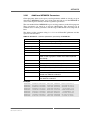
Addressing the M-Modules
The PowerPC can address M-Modules via the local PCI bus. The PCI-to-M-Module
bridge is implemented in an FPGA. The three M-Modules are mapped within the
PCI target as shown in the following table. The address determines the access mode
in which the respective M-Module is addressed. The interrupt of each M-Module
can be handled in the Control/Status Register. The interrupts of all M-Modules are
summarized in the bridge as the PCI interrupt of this target device.
Table 2. M-Module address map
Base Address
Register/
Block Size
M-Module 0
32M
Offset Address Range
Function
0x 0000 0000..0x 00FF FFFF A24/D32 access
0x 0100 0000..0x 01FF FCFF A24/D16 access
0x 01FF FD00..0x 01FF FDFF A08/D32 access
0x 01FF FE00..0x 01FF FEFF A08/D16 access
0x 01FF FF00..0x 01FF FF03 A08/D16 IACK
0x 01FF FF04..0x 01FF FF07 Control/Status Register
M-Module 1
32M
0x 0200 0000..0x 02FF FFFF A24/D32 access
0x 0300 0000..0x 03FF FCFF A24/D16 access
0x 03FF FD00..0x 03FF FDFF A08/D32 access
0x 03FF FE00..0x 03FF FEFF A08/D16 access
0x 03FF FF00..0x 03FF FF03 A08/D16 IACK
0x 03FF FF04..0x 03FF FF07 Control/Status Register
M-Module 2
32M
0x 0400 0000..0x 04FF FFFF A24/D32 access
0x 0500 0000..0x 05FF FCFF A24/D16 access
0x 05FF FD00..0x 05FF FDFF A08/D32 access
0x 05FF FE00..0x 05FF FEFF A08/D16 access
0x 05FF FF00..0x 05FF FF03 A08/D16 IACK
0x 05FF FF04..0x 05FF FF07 Control/Status Register
0x 0600 0000..0x 07FF FFFF Reserved for FPGA user
functions
MEN Mikro Elektronik GmbH
20A012-00 E4 – 2012-12-03
33
Functional Description
M-Module Control/Status Register (0xnFFFF04) (read/write)
15..4
3
-
BE
2
1
0
PCIIEN IRQ
RET
BE
Bus error
1 = Bus error occurred. Write 1 to clear.
PCIRET PCI retries
0 = PCI retries during access (slower)
1 = No PCI retries during access (faster) (default)
You should change this setting to 0 ("slower") if you can expect the
M-Module access to be slower than 450 ns. Otherwise, leave the default
setting as is.
IEN
Interrupt enable bit
0 = Disable interrupt
1 = Enable interrupt
IRQ
Interrupt pending
1 = Interrupt pending (reflects inverted M_IRQ line)
2.7.3
Installing an M-Module Mezzanine Module
Perform the following steps to install an M-Module:
Power down your system and remove the CPU board from the system.
Remove the filler panel from the board’s front M-Module slot, if installed.
Loosen the two front-panel mounting screws at the solder side of the CPU
board and remove the whole front panel (see Figure 3, A12B board map – CPU
board with M-Modules – top view, on page 20).
Hold the M-Module over the target slot of the CPU board with the component
sides facing each other.
Align the 60-pin connectors of the M-Module and carrier board.
Press the M-Module carefully but firmly onto the CPU board, making sure that
the connectors are properly linked.
Turn the CPU board upside down and use four M-Module mounting screws to
fasten the M-Module on the solder side of the board.
You can order suitable mounting screws from MEN. Please see the A12B pages
on MEN’s website for ordering options.
MEN Mikro Elektronik GmbH
20A012-00 E4 – 2012-12-03
34
Functional Description
Figure 7. Installing an M-Module mezzanine module (A12B)
M‐Module
Mounting bolt
60‐pin connector
CPU board without front panel
M3x6 cross‐recess pan‐head screws
MEN Mikro Elektronik GmbH
20A012-00 E4 – 2012-12-03
M3x6 slotted pan‐
head screws (plastics)
35
Functional Description
2.8
PMC Slots (A12C)
The A12 board provides two PMC slots for extension such as graphics, Fast
Ethernet, SCSI etc. The market offers lots of different PMC mezzanines.
!
The signaling voltage is set to 3.3 V, i. e. the CPU board has no voltage key (see
Figure 8, Installing a PMC mezzanine module (A12C), on page 37) and can only
carry PMC mezzanines that support this keying configuration. Mezzanine cards
may be designed to accept either or both signaling voltages (3.3 V / 5 V).
The connector layout is fully compatible to the IEEE1386 specification. For
connector pinouts please refer to the specification (see Chapter 5.1 Literature and
Web Resources on page 98).
Connector types:
• 64-pin, 1-mm pitch board-to-board receptacle according to IEEE 1386
• Mating connector:
64-pin, 1-mm pitch board-to-board plug according to IEEE 1386
2.8.1
Installing a PMC Mezzanine Module
Perform the following steps to install a PMC module:
Make sure that voltage keying of your PMC module matches the CPU board.
Power down your system and remove the CPU board from the system.
Remove the filler panel from the board’s front PMC slot, if installed.
The PMC module is plugged on the board with the component sides of the
PCBs facing each other.
Put the PMC module’s front connector through the front slot at a 45° angle.
Carefully put it down, making sure that the connectors are properly aligned.
Press the PMC module firmly onto the board.
Make sure that the EMC gasket around the PMC front panel is properly in its
place.
Screw the PMC module tightly to the CPU board at the bottom side of the PCB
using four oval-head cross-recessed screws of type M2.5x6.
You can order suitable mounting screws from MEN. Please see the A12B pages
on MEN’s website for ordering options.
MEN Mikro Elektronik GmbH
20A012-00 E4 – 2012-12-03
36
Functional Description
Figure 8. Installing a PMC mezzanine module (A12C)
PMC module
Mounting standoff
64‐pin connectors
CPU board
2 M2.5x6 oval‐head cross‐recessed screws
MEN Mikro Elektronik GmbH
20A012-00 E4 – 2012-12-03
2 M2.5x6 oval‐head cross‐recessed screws
37
Functional Description
2.9
IDE Interface
The board provides a 44-pin plug for IDE connection. The pinning of this connector
is compliant with the ATA-4/ATAPI specification.
See Figure 1, General board map – top view, on page 18 for the position of the IDE
connector.
Connector types:
• 44-pin, 2-row SMT plug, 2 mm pitch
• Mating connector:
44-pin, 2-row IDC receptacle, 2 mm pitch
Table 3. Pin assignment of the 44-pin IDE connector
44
2
MEN Mikro Elektronik GmbH
20A012-00 E4 – 2012-12-03
43
1
44
GND
43
GND
42
+5V
41
+5V
40
GND
39
IDE_RACT#
38
IDE_RCS3#
37
IDE_RCS1#
36
IDE_RA[2]
35
IDE_RA[0]
34
-
33
IDE_RA[1]
32
-
31
IDE_RIRQ
30
GND
29
IDE_RDAK#
28
GND
27
IDE_RRDY
26
GND
25
IDE_RRD#
24
GND
23
IDE_RWR#
22
GND
21
IDE_RDRQ
20
-
19
GND
18
IDE_RD[15]
17
IDE_RD[0]
16
IDE_RD[14]
15
IDE_RD[1]
14
IDE_RD[13]
13
IDE_RD[2]
12
IDE_RD[12]
11
IDE_RD[3]
10
IDE_RD[11]
9
IDE_RD[4]
8
IDE_RD[10]
7
IDE_RD[5]
6
IDE_RD[9]
5
IDE_RD[6]
4
IDE_RD[8]
3
IDE_RD[7]
2
GND
1
IDE_RRST#
38
Functional Description
Table 4. Signal mnemonics for the IDE connector
Signal
Direction
Function
+5V
-
+5V power supply, current-limited to 1.5A by a fuse
GND
-
Digital ground
IDE_RA[2:0]
out
IDE address [2:0]
IDE_RACT#
in
IDE active
IDE_RCS1#
out
IDE chip select 1
IDE_RCS3#
out
IDE chip select 3
IDE_RD[15:0]
in/out
IDE data [15:0]
IDE_RDAK#
out
IDE DMA acknowledge
IDE_RDRQ
in
IDE DMA request
IDE_RIRQ
in
IDE interrupt request
IDE_RRD#
out
IDE read strobe
IDE_RRDY
in
IDE ready
IDE_RRST#
out
IDE reset
IDE_RWR#
out
IDE write strobe
2.9.1
Fuse Protection
The IDE power supply is protected by a fuse. This fuse is not intended to be
exchanged by the customer. Your warranty for the A12 will cease if you
exchange the fuse on your own. Please send your board to MEN for repair if a fuse
blows.
•
•
•
•
Current rating: 3A
Type: fast
Size: 1206
MEN part number: 5675-0003
The fuse is located on the top side of A12.
Figure 9. Position of fuse for IDE power supply protection
Fuse
IDE Interface
Front‐panel mounting screw
MEN Mikro Elektronik GmbH
20A012-00 E4 – 2012-12-03
39
Functional Description
2.9.2
Installing a Hard Disk
A hard-disk adapter card for installation of a 2.5", 9.5mm hard-disk drive is
available from MEN. The adapter is designed in such a way that standard hard disks
can easily be installed. For flexibility the adapter does not include the hard disk
itself but includes all necessary screws to mount a standard hard disk.
Please see the A12B pages on MEN’s website for ordering options.
If you want to install a hard disk on the board using MEN’s adapter card, please
keep in mind that the assembly occupies some of the space usually used for
mezzanine modules. See Chapter 1.1 Maps of the Board on page 18 and Figure 11,
Position of hard-disk adapter card on the board, on page 41.
The board needs only one slot in the system even with a hard disk installed. In this
case no component pins of neighboring boards may exceed the interboard
separation plane.
Figure 10. A12C with hard-disk adapter and hard disk
MEN Mikro Elektronik GmbH
20A012-00 E4 – 2012-12-03
40
Functional Description
Figure 11. Position of hard-disk adapter card on the board
Front‐panel mounting screw
CompactFlash
card connector
MPC8245
1
VMEbus P1
LAN 1
CompactFlash
metal holder
I/O Connector
Reset Button/LED
RS232 COM1
SO‐DIMM
DRAM Socket
LAN 2
Production/Test
User‐
configurable hex switch
Front Panel
Side of Board
M1543
ALI
Hard‐disk adapter
IDE Interface
Front‐panel mounting screw
MEN Mikro Elektronik GmbH
20A012-00 E4 – 2012-12-03
41
Functional Description
2.10
Ethernet Interface
The two Ethernet interfaces of the A12 support 10 Mbit/s and 100 Mbit/s as well as
full-duplex operation and autonegotiation.
!
The unique MAC address is set at the factory and should not be changed. Any
attempt to change this address may create node or bus contention and thereby render
the board inoperable. The MAC addresses on A12 are:
• LAN1:
• LAN2:
0x 00 C0 3A 17 xx xx
0x 00 C0 3A 18 xx xx
where "00 C0 3A" is the MEN vendor code, "17" and "18" are the MEN product
codes, and "xx xx" is the hexadecimal serial number of the product, which depends
on your board, e. g. "... 00 2A" for serial number "000042". (See Chapter 5.2
Finding out the Board’s Article Number, Revision and Serial Number on page 100.)
2.10.1
Connection
Two standard RJ45 connectors with status LEDs are available at the front panel for
connection to 10Base-T or 100Base-TX network environments. It is not necessary
to switch between the two configurations!
The pin assignment corresponds to the Ethernet specification IEEE 802.3.
Connector types:
• Modular 8/8-pin mounting jack according to FCC68
• Mating connector:
Modular 8/8-pin plug according to FCC68
Table 5. Pin assignment and status LEDs of the 8-pin RJ45 Ethernet 10Base-T/
100Base-T connectors
Lights up whenever there is
transmit or receive activity
ACT
1
Lights up as soon as the
link is established
(10Base-T or 100Base-T)
LNK
8
1
TX+
2
TX-
3
RX+
4
Shield_R
5
Shield_R
6
RX-
7
Shield_R
8
Shield_R
Table 6. Signal mnemonics of the Ethernet 10Base-T/100Base-T connectors
Signal
Function
Shield_R
-
Shield via RC network
RX+/-
in
Differential pair of receive data lines
TX+/-
out
Differential pair of transmit data lines
MEN Mikro Elektronik GmbH
20A012-00 E4 – 2012-12-03
Direction
42
Functional Description
2.11
I/O Expansion Connector
The board features a 40-pin I/O connector that implements several interfaces:
• Serial port COM2 (compatible with MEN’s SA-Adapters, see Chapter 2.12
Serial Ports COM1..COM4 on page 46)
• Serial ports COM3 and COM4 of the MPC8245
• Reset and abort signals
• Two user-configurable LEDs
• Keyboard/mouse (PS/2)
• USB 1.1 port
You can easily connect these interfaces using the AD67 I/O extension card from
MEN, which plugs directly to the 40-pin connector, has convenient SA-Adapter
slots and forms a 1-slot side card with additional front-panel connectors.
Please see the A12B pages on MEN’s website for ordering options and the AD67
pages for more information.
Connector types:
• 40-pin low-profile plug, 2.54 mm pitch, for ribbon-cable connection
• Mating connector:
40-pin IDC receptacle, e.g. Elco Series 8290 IDC socket
Table 7. Pin assignment of the 40-pin I/O expansion connector
40
2
1
1
Reserved1
39
Reserved
38
Reserved
37
Reserved
36
Reserved
35
Reserved
34
Reserved
33
Reserved
32
RXD4
31
Reserved
30
TXD4
29
Reserved
28
RXD3
27
TXD3
26
+5V
25
GND
24
USBP0+
23
USBP0-
22
+5V
21
GND
20
MSDATA
19
MSCLK
18
KBDATA
17
KBCLK
16
LED2
15
LED1
14
ABRTBTN#
13
PWRBTN#
12
+5V
11
GND
10
RI2#
9
DCD2#
8
CTS2#
7
DSR2#
6
RTS2#
5
DTR2#
4
RXD2
3
TXD2
2
+5V
1
GND
Reserved pins cannot be used but do not impair functionality.
MEN Mikro Elektronik GmbH
20A012-00 E4 – 2012-12-03
39
40
43
Functional Description
Table 8. Signal mnemonics of 40-pin I/O expansion connector
Signal
-
+5V power supply
GND
-
Digital ground of respective interface
KBDATA
out
Keyboard data
KBCLK
out
Keyboard clock
MSDATA
out
Mouse data
MSCLK
out
Mouse clock
LED1
out
LED1 cathode1
LED2
out
LED2 cathode1
ABRTBTN#
in
Abort button2
PWRBTN#
in
Reset button2
CTS2#
in
Serial port COM2 clear to send
DCD2#
in
Serial port COM2 data carrier detect
DSR2#
in
Serial port COM2 data set ready
DTR2#
out
Serial port COM2 data terminal ready
RI2#
in
Serial port COM2 ring indicator
RTS2#
out
Serial port COM2 request to send
RXD2
in
Serial port COM2 receive data
TXD2
out
Serial port COM2 transmit data
RXD3
in
Serial port COM3 receive data
(MPC8245)
TXD3
MPC8245
COM3/
RXD4
COM4
out
Serial port COM3 transmit data
(MPC8245)
in
Serial port COM4 receive data
(MPC8245)
TXD4
out
Serial port COM4 transmit data
(MPC8245)
USBP0+,
USBP0-
in/out
USB port differential pair
Mouse/
Keyboard
LEDs
Button
M1543
COM2
USB
Connect the anode to +5 V (pin 12 of 40-pin connector).
Connect the button’s second terminal to GND (pin 11 of 40-pin connector).
MEN Mikro Elektronik GmbH
20A012-00 E4 – 2012-12-03
Function
+5V
Power
1
2
Direction
44
Functional Description
2.11.1
!
Fuse Protection
The I/O connector is protected by a fuse. This fuse is not intended to be
exchanged by the customer. Your warranty for the A12 will cease if you
exchange the fuses on your own. Please send your board to MEN for repair if a
fuse blows.
•
•
•
•
Current rating: 1.5 A
Type: fast
Size: 1206
MEN part number: 5675-0001
The fuses are located on the top side of A12.
Figure 12. Position of fuse for I/O connector protection
Front‐panel mounting screw
Fuse
LAN 1
CompactFlash
metal holder
CompactFlash
card connector
MPC8245
1
I/O Connector
t Button/LED
RS232 COM1
SO‐DIMM
DRAM Socket
LAN 2
Production/Test
MEN Mikro Elektronik GmbH
20A012-00 E4 – 2012-12-03
User‐
configurable hex switch
45
Functional Description
2.12
Serial Ports COM1..COM4
The onboard Super I/O controller Ali M1543 provides two high-performance 16550
compatible UARTs with 16-byte send/receive FIFOs and a programmable baud rate
generator. These UARTs are used as COM1 and COM2.
The MPC8245 provides another two UARTs, used as COM3 and COM4.
You can set the baud rate through MENMON.
2.12.1
COM1
COM1 is a standard RS232 interface led to an RJ45 connector at the front panel.
Connector types:
• Modular 8/8-pin mounting jack according to FCC68
• Mating connector:
Modular 8/8-pin plug according to FCC68
Table 9. Pin assignment of 8-pin RJ45 RS232 connector (COM1)
1
1
DSR
2
DCD
3
DTR
4
GND
5
RXD
6
TXD
7
CTS
8
RTS
8
2.12.2
COM2..COM4
COM2..COM4 are available via the 40-pin I/O connector. The signal level is fixed
to TTL. This allows flexible line interface configuration using serial interface (SA)
adapters.
COM2..COM4 support the use of MEN’s standard SA-Adapters. This allows you to
choose from a number of available line interfaces, from RS232 to RS422/RS485 to
TTY, with or without optical isolation.
COM2 is a full-fledged serial interface, while COM3 and COM4 only provide basic
serial lines and have no handshake lines.
For pin assignments of COM2..COM4 please refer to Chapter 2.11 I/O Expansion
Connector on page 43.
MEN offers a mounting kit for connection of standard SA-Adapters.
For compatible adapters and the mounting kit please see the A12B pages on
MEN’s website.
MEN Mikro Elektronik GmbH
20A012-00 E4 – 2012-12-03
46
Functional Description
2.12.2.1 Installing Standard SA-Adapters
You can install SA-Adapters either through ribbon-cable connection directly on the
40-pin I/O connector, or using an additional I/O extension card, MEN’s AD67.
Please see Chapter 2.11 I/O Expansion Connector on page 43 and MEN’s website
for more information. The following description shows how to install SA-Adapters
without any extension card.
!
Note: MEN gives no warranty on functionality and reliability of the board and SAAdapters used if you install SA-Adapters in a different way than described in
this manual.
Perform the following steps to install standard SA-Adapters using MEN’s mounting
kit:
Power-down your system and remove the board from the system.
Remove the two front panel screws and the two screws on top of the mounting
bolts of the SA-Adapter.
Use the front panel screw to fasten the SA-Adapter at the additional SAAdapter front panel.
Plug the prefolded ribbon cable to the 40-pin I/O connector on the board.
Plug the two 10-pin connector of the ribbon cable to the respective SA-Adapter
connector.
Make sure to always match the pins correctly (pin 1 is marked by a triangle on
the ribbon cable connector).
You can now reinsert the board and the additional front panel into your system.
Make sure to fasten the SA-Adapter front panel appropriately in your enclosure!
MEN Mikro Elektronik GmbH
20A012-00 E4 – 2012-12-03
47
Functional Description
2.13
Temperature Sensor
The LM75 temperature sensor is used for temperature management. It continuously
measures the board temperature.
2.14
Real-Time Clock and NVRAM
The board includes the 41T56 SMB real-time clock with integrated NVRAM. A
local GoldCap capacitor supplies the backup voltage. The real-time clock must be
supplied via the VMEbus STANDBY line.
The 56-byte NVRAM is organized as a 56 bytes x 8 bits SRAM.
2.15
Watchdog
The board uses an SMS24 watchdog, which has three functions:
• Power-On Reset
• Watchdog
• EEPROM (2 KB) (see Chapter 2.5.4 EEPROM on page 29)
2.16
User-Defined Hex Switch
The board provides a rotary hex switch for operating system requirements and user
applications. Please refer to the corresponding software manual for their
implementation.
Figure 13. Position of hex switch
Front‐panel mounting screw
CompactFlash
card connector
MPC8245
1
SO‐DIMM
DRAM Socket
LAN 2
Production/Test
MEN Mikro Elektronik GmbH
20A012-00 E4 – 2012-12-03
User‐
configurable hex switch
VMEbus P1
LAN 1
CompactFlash
metal holder
I/O Connector
Reset Button/LED
RS232 COM1
48
Functional Description
2.17
VMEbus Interface
The board's VMEbus interface conforms to the VMEbus specification. It has the
following features:
• Slot-1 functionality with auto-detection
• Wide range of VMEbus address and data transfer modes
•
•
•
•
•
•
- Master D08(EO):D16:A24:A16:RMW1
- Slave D08(EO):D16:A24:BLT
Interrupt handler: 7-level, D08(O):IH(7-1)
Interrupter: 7-level, D08(O):I(7-1):ROAK
Single level 3 fair requester
Single level 3 arbiter
BTO bus timeout
Access to 1 MB shared fast SRAM or to PCI space
2.17.1
SRAM
The SRAM is accessible from the VMEbus, the VME address can be configured in
steps of up to 1 MB in the SLV – Slave Control Register (0x14) (read/write).
Access from the VMEbus can be disabled.
The SRAM has a size of 1 MB. It is accessible via block and standard transfers (user
and supervisor space).
See also Table 26, VMEbus memory mapping, on page 93.
2.17.2
Slot-1 Function
The slot-1 function is auto-detected. It can be read from the SYSCTL register (bit
SYSCON).
2.17.3
Interrupter
The board has one interrupter. It can generate an interrupt on all seven levels, which
can be configured through bits ILx in the INTR – VME Interrupter Control Register
(0x00) (read/write). The interrupt vector is written to register INTID – VME
Interrupt STATUS/ID Register (0x04) (read/write). An interrupt request is
generated by setting bit INTEN in the INTR register. This bit is cleared in the IACK
cycle.
1
For RMW cycles PCI to VME only byte/word (8-bit/16-bit) accesses are allowed!
MEN Mikro Elektronik GmbH
20A012-00 E4 – 2012-12-03
49
Functional Description
2.17.4
Interrupt Handler
The board can receive interrupts on all seven levels. In addition, it can handle
ACFAIL interrupts. You can mask interrupts through the IMASK – Interrupt Mask
Register (0x0C) (read/write).
If a VME interrupt occurs that is not masked, the PCI-to-VME bridge generates a
PCI interrupt (routed to INT_B on board). Then, the software must read the ISTAT –
Interrupt Status Register (0x08) (read/write) to detect which VME interrupts are
pending. The ISTAT register will only show bits that were enabled in IMASK!
The interrupt vector must then be fetched through a read to the VME IACK space.
The address within the IACK space must reflect the VMEbus level (e.g. word access
0xA or byte access 0xB for level 5).
Naturally, there is no vector for ACFAIL interrupts. To reset such interrupts, write 1
to the ACFST bit in ISTAT – Interrupt Status Register (0x08) (read/write).
2.17.5
Bus Errors
If a bus error occurs, bit BERR in the MSTR – Master Control Register (0x10)
(read/write) is set. An interrupt is triggered if the IBERREN Bit in the MSTR –
Master Control Register (0x10) (read/write) is set. The timeout for BERR is 60 μs.
The bus error can be cleared by writing 1 to the BERR bit.
2.17.6
Master Access
The address modifiers for master access are always
• 0x39 = Standard user data access for A24:D16, standard I/O
• 0x29 = Short user access for A16:D16, short I/O
2.17.7
Atomic Operations
CPU-to-SRAM Operations
Not supported.
CPU-to-VME Operations
Read-Modify-Write operations to the VMEbus can be done via bit RMW in the
MSTR – Master Control Register (0x10) (read/write). Only byte and word accesses
are allowed, with word accesses being made to even addresses.
VME-to-SRAM Operations
Supported.
MEN Mikro Elektronik GmbH
20A012-00 E4 – 2012-12-03
50
Functional Description
2.17.8
PCI Configuration Space Registers
The Configuration Registers from 0x00 to 0x3C conform with the PCI Device
Configuration Header Format.
Table 10. PCI Configuration Space Registers
Byte
Address
2
1
0
0x00
Device ID (0x5056)
Vendor ID (0x1172)
0x04
Status Register
Command Register
0x08
Class Code (0x068000)
0x0C
BIST
0x10
Base Address Register 0
0x14
This register is always 0.
0x18
This register is always 0.
0x1C
This register is always 0.
0x20
This register is always 0.
0x24
This register is always 0.
0x28
Card Bus CIS Pointer
0x2C
Subsystem ID
0x30
Expansion ROM Base Address Register
0x34
Reserved
0x38
Reserved
0x3C
Maximum
Latency
MEN Mikro Elektronik GmbH
20A012-00 E4 – 2012-12-03
3
Header Type
Revision ID
(currently
0x01)
Latency Timer
Cache Line
Size
Subsystem Vendor ID
Minimum Grant Interrupt Pin
Interrupt Line
51
Functional Description
2.17.9
Runtime Registers
The registers are not directly accessible from the VMEbus but from the PCI bus.
Writes to registers can only be done through the PCI bus (read/write registers) or
from the bridges internal modules. Read only registers can not be written from the
PCI bus, only from the internal modules.
The address of these registers can be computed by reading out BAR0 of the PCI-toVME bridge's PCI configuration space. Then add 0x01800000 plus the register
offset to this value.
INTR – VME Interrupter Control Register (0x00) (read/write)
7..4
3
2
1
0
-
INTEN
IL2
IL1
IL0
This register controls the internal interrupter. Interrupt levels from 1 to 7 can be set.
The interrupt is generated only when the INTEN bit is set.
INTEN
ILx
0 = Interrupt disabled (default)
1 = Enable interrupt at level specified through ILx
The interrupt level is set in binary code (e. g. ILx=011 is IRQ3).
Default: 0x0
INTEN should be set after the ILx bits are set to avoid glitches on the IRQ lines.
INTEN is automatically cleared during the acknowledge cycle and the request is
removed (ROAK). The ILx bits, however, remain set until they are overwritten.
Check the INTEN bit to verify that the interrupt has been acknowledged.
INTID – VME Interrupt STATUS/ID Register (0x04) (read/write)
7..0
INT_ID
In this Register, the STATUS/ID of the internal interrupter is set.
INT_ID The STATUS/ID of the interrupt that the external handler reads during the
IACK cycle.
Default: 0x00
MEN Mikro Elektronik GmbH
20A012-00 E4 – 2012-12-03
52
Functional Description
ISTAT – Interrupt Status Register (0x08) (read/write)
7
6
5
4
3
2
1
0
I7
I6
I5
I4
I3
I2
I1
ACFST
Ix
The PCI Master can read the asserted interrupts here if they are not
masked in the IMASK register. Interrupts are reset automatically if the
external interrupter removes its request. Writes to these bits are ignored.
ACFST If this reads 1, an ACFAIL# interrupt has occurred. This interrupt is stored,
because it is not static. It can be cleared by writing 1.
Default: 0
In order to read the interrupt STATUS/ID from the interrupter, the CPU must
generate a read cycle to the IACK memory area by setting the last significant
address bits A[3..1] to the corresponding interrupt level (e. g. for IRQ5# set A[3:1]
to [101]).
IMASK – Interrupt Mask Register (0x0C) (read/write)
7
6
5
4
3
2
1
0
IEN7
IEN6
IEN5
IEN4
IEN3
IEN2
IEN1
ACFEN
IENx
If the corresponding interrupt pin IRQx is asserted, the bridge will signal
an interrupt to the PCI side (INTA#).
0 = Interrupt masked (default)
1 = Interrupt enabled
ACFEN When this bit is set, and an ACFAIL# is detected, an interrupt on the PCI
side is generated.
0 = Interrupt masked (default)
1 = ACFAIL interrupt enabled
MSTR – Master Control Register (0x10) (read/write)
7..5
-
4
3
POSTWR IBERREN
2
1
0
BERR
REQ
RMW
POSTWR Posted Write Access to VMEbus
0 = Delayed write access to VMEbus (default)
1 = Posted write access to VMEbus
IBERREN This bit enables an interrupt to PCI if a VMEbus BERR# signal occurs.
This interrupt is level-triggered!
0 = Interrupt disable (default)
1 = Interrupt enable
BERR
Monitor for VMEbus BERR# signal
0 = No VMEbus error (default)
1 = VMEbus error occurred, cleared by writing 1
MEN Mikro Elektronik GmbH
20A012-00 E4 – 2012-12-03
53
Functional Description
REQ
RMW
Set VMEbus requester scheme
0 = Release On Request (ROR) (default)
1 = Release When Done (RWD)
If this bit is changed from 0 to 1, i. e. from ROR to RWD, and there
were previous accesses over the master interface, it is recommended to
do a dummy read to free the bus.
Enable single Read-Modifiy-Write-Cycle
0 = Normal cycle (default)
1 = RMW cycle. Master keeps AS# asserted during back-to-back read/
write cycle.
This bit is automatically cleared after the RMW cycle and must be set
for the next RMW cycle again.
Note: During RMW cycles all interrupts on the host CPU should be masked.
SLV – Slave Control Register (0x14) (read/write)
7..5
4
3..0
-
SLEN
SLBASE
SLEN
0 = Slave Unit disabled (default)
1 = Slave Unit enabled
SLBASE The slave's base address. Specifies the lowest address in the VMEbus
address range that will be decoded. This field will be compared with the
VME address A[23:20]. Since only A[23:20] are monitored, the smallest
possible address space is 1 MB.
Default: 0000
SYSCTL – System Controller Register (0x18) (read/write)
7..3
2
1
0
-
ATO
SYSRES
SYSCON
ATO
Monitor for Arbitration Timeout Signal
0 = No Arbitration Timeout (default)
1 = Arbitration Timeout occurred (after approx. 124 μs), cleared by
writing 1
SYSRES Reset VMEbus
0 = No assertion of SYSRES# (default)
1 = Assert output pin SYSRES#
SYSCON If set to 1, the system controller unit is enabled. This is only allowed if the
board resides in VMEbus slot 1. The state after reset depends on
successful automatic detection of the board’s location. If this bit is set
after reset but the board is not in slot 1, detection fails and the bit must be
cleared manually.
When set, the Arbiter, Arbitration Timer, Bus Timer and IACK-DaisyChain Driver are enabled.
MEN Mikro Elektronik GmbH
20A012-00 E4 – 2012-12-03
54
Functional Description
2.17.10
Connection
Connector types:
• Type-C 96-pin plug connector according to DIN41612/MIL-C-55302/IEC603-2
• Mating connector:
Type-C 96-pin receptacle according to DIN41612/MIL-C-55302/IEC603-2
Table 11. Pin assignment of 3-row, 96-pin VMEbus connector P1
ABC
1
32
MEN Mikro Elektronik GmbH
20A012-00 E4 – 2012-12-03
A
B
C
1
D0
BBSY#
D8
2
D1
-
D9
3
D2
ACFAIL#
D10
4
D3
BG0IN#
D11
5
D4
BG0OUT#
D12
6
D5
BG1IN#
D13
7
D6
BG1OUT#
D14
8
D7
BG2IN#
D15
9
GND
BG2OUT#
GND
10
SYSCLK
BG3IN#
-
11
GND
BG3OUT#
BERR#
12
DS1#
-
SYSRESET#
13
DS0#
-
LWORD#
14
WRITE#
-
AM5
15
GND
BR3#
A23
16
DTACK#
AM0
A22
17
GND
AM1
A21
18
AS#
AM2
A20
19
GND
AM3
A19
20
IACK#
GND
A18
21
IACKIN#
-
A17
22
IACKOUT#
-
A16
23
AM4
GND
A15
24
A7
IRQ7#
A14
25
A6
IRQ6#
A13
26
A5
IRQ5#
A12
27
A4
IRQ4#
A11
28
A3
IRQ3#
A10
29
A2
IRQ2#
A9
30
A1
IRQ1#
A8
31
-12V
+5VSTDBY
+12V
32
+5V
+5V
+5V
55
MENMON
3
MENMON
3.1
General
MENMON is an assembly-language debugger with a simple user console interface
and can easily be extended and ported.
MENMON for A12 also uses some parts of Motorola’s DINK32 and provides
extensions for user interface, configuration, debugging and self test.
Purpose
• Debugging applications without any operating system
• Bootstrapping operating systems
• Hardware testing
Features
• Auto-configuration for PCI devices on the board and devices on secondary PCI
buses
• Interrupt routing of all onboard devices and of all devices on secondary PCI
buses
• SDRAM size detection, reading and checking (Serial Presence Detect Data
Structure)
• Flash programming with password protection of MENMON spaces
• Primary/secondary MENMON
• Subset of Motorola PPCBug system calls implemented
3.2
Console
MENMON for the board can communicate through the COM1 port (available
through the I/O connector).
Additionally, if a P1 graphics PC-MIP module is found on the PCI bus, any console
output will also appear on the VGA display. The same is true if you connect a PS/2
keyboard to the I/O connecter. Characters can then be entered on the RS232 console
and on the PS/2 keyboard.
The default setting of the COM ports is 9600 baud, eight data bits, no parity, one
stop bit.
MEN Mikro Elektronik GmbH
20A012-00 E4 – 2012-12-03
56
MENMON
3.3
MENMON Memory Map
Figure 14. MENMON – Address mapping
0x 0000 0000
Exception W rappers
0x 0000 3000
MENMON Parameter String
0x 0000 3200
Unused
0x 0000 4200
VxW orks Bootline
12 KB
512 bytes
4 KB
256 bytes
0x 0000 4300
Unused
16 MB
Download Area for
SERDL
DBOOT
NBOOT
15 MB
MENMON relocated code
Global Data
512 KB
0x 01F8 0000
MENMON Stack
64 KB
0x 01F9 0000
User Program Stack
64 KB
MENMON Memory Pool (malloc)
384 KB
Runaway Stack
64 KB
0x 0100 0000
0x 01F0 0000
0x 01FA 0000
0x 01FF 0000
MEN Mikro Elektronik GmbH
20A012-00 E4 – 2012-12-03
57
MENMON
3.4
MENMON Start-up
3.4.1
User LEDs
There are two LEDs available on the I/O connector (see Chapter 2.11 I/O Expansion
Connector on page 43). The LEDs display the state of the boot like a counter.
!
The exact sequence of the LEDs, i. e. when each LED will light, depends on the
MENMON version. If you have any problems during start-up, please turn to MEN’s
support at [email protected] and give your MENMON version.
3.4.2
Boot Sequence
The assembler part of MENMON initializes the CPU and the host-to-PCI bridge
integrated in the MPC8245 (memory interface), and the monitor will be relocated to
the main memory.
All known devices will be initialized.
The primary MENMON looks for a valid secondary MENMON and starts it unless
the ABORT button is pressed, which is available on the I/O connector. ("Valid"
means the size is between 0x0000 and 0x80000 and the checksum is valid.)
If you press the ABORT button for more than five seconds, the MENMON settings
in the EEPROM are restored with default values.
MENMON checks whether there is a valid "startup" string stored in EEPROM. If
valid, all commands in the "startup" string are executed. (See Chapter 3.4.3
Configuring the MENMON Start-up Procedure on page 58.)
If no startup string was present, MENMON jumps to the operating system
bootstrapper whose address can be configured using the EE-BS command.
The MENMON command line interface will appear if the ESC key is pressed or the
bootstrapper address is set to an invalid address (i. e. 0x0 or 0xFFFFFFFF)
3.4.3
Configuring the MENMON Start-up Procedure
MENMON can be configured to automatically execute commands at start-up, for
example to boot from disk. The EE-STARTUP command can be used to configure
these commands. The EEPROM stores a string (max. 79 characters) that is
comprised of commands that are executed at startup, e.g:
DBOOT 1 FILE=MYBOOT; NBOOT
MENMON performs these commands until one of the commands passes control to a
loaded image.
The "EE-STARTUP -" command can be used to deactivate autoexecution of the
string. When the string is inactive, MENMON calls its BO command at start-up.
MEN Mikro Elektronik GmbH
20A012-00 E4 – 2012-12-03
58
MENMON
3.4.4
Self Tests
At start-up the monitor runs self tests depending on the current self test level. (OFF,
QUICK or EXTENDED). The MENMON behavior depends on the current stop on
error mode (NO HOLD or HOLD).
Power On Self Test output with self test message mode EXTENDED:
=== PCI ===
MPC107
ALI1543 PCI2ISA
ALI1543 IDE
ALI1543 PMU
Enet 82559 I
Enet 82559 II
M-Mod Bridge
VME Bridge
PC-MIP/PMC Bridge
CPCI Bridge
CPCI slot 2
CPCI slot 3
CPCI slot 4
CPCI slot 5
CPCI slot 6
CPCI slot 7
CPCI slot 8
SO-SIMM SPD
RTC
LM75
HEX-SW
CHECKSUM
3.4.4.1
bus
bus
bus
bus
bus
bus
bus
bus
bus
bus
bus
bus
bus
bus
bus
bus
bus
===
==>
==>
==>
===
==>
===
==>
0x0, dev 0x00
0x0, dev 0x12
0x0, dev 0x1B
0x0, dev 0x1C
0x0, dev 0x17
0x0, dev 0x1A
0x0, dev 0x18
0x0, dev 0x19
0x0, dev 0x1D
0x0, dev 0x1E
0x1, dev 0x0F
0x1, dev 0x0E
0x1, dev 0x0D
0x1, dev 0x0C
0x1, dev 0x0B
0x1, dev 0x0A
0x1, dev 0x09
SMB ===
OK
OK
OK
HEX ===
OK
FLASH ===
OK
==>
==>
==>
==>
==>
==>
==>
==>
==>
==>
==>
==>
==>
==>
==>
==>
==>
OK
OK
OK
OK
OK
OK
OK
NOT
NOT
OK
NOT
NOT
NOT
NOT
NOT
NOT
NOT
PRESENT
PRESENT
PRESENT
PRESENT
PRESENT
PRESENT
PRESENT
PRESENT
PRESENT
Self Tests in Detail
Self tests can be manually started using the command DIAG xxx, e.g. DIAG RTC.
DIAG ALL executes all self tests.
RTC
The RTC test is non-destructive. It writes and compares the RTC NVRAM.
MEN Mikro Elektronik GmbH
20A012-00 E4 – 2012-12-03
59
MENMON
PCI
This test scans the PCI bus with configuration cycles for PCI devices. This test
checks if all required devices are present. An error is reported if one of the following
devices is missing:
• Integrated host-to-PCI bridge of MPC8245
• ALI1543
• Ethernet I
MENMON also checks for the following optional devices, but the absence of these
devices is not treated as an error:
•
•
•
•
•
Ethernet II
M-Module bridge
VMEbus bridge
CompactPCI bridge
CompactPCI slots
SMB
This test performs read accesses to all on-board SMB devices.
Hex Switch
This test reads and displays the current hex switch position.
MENMON Flash Checksum
This test checks the checksum of the current MENMON (primary/secondary). The
first long word of MENMON contains the size, the second long word contains the
expected checksum. The test computes the checksum by XORing each long word of
MENMON with the next one, except for the first two long words.
ABORT Button
This test checks pressing and releasing of the ABORT button to test port pin GPI 0
of the M1543 (cf. Chapter 4.3 Implementation of M1543 PCI-to-ISA Bridge on
page 95).
The test is not performed during Power On Self Test.
This test does not check the ABORT interrupt.
CPU
This test enters and displays the clock configuration.
The test is not performed during Power On Self Test.
An error is detected for unknown PLL configuration for the installed CPU type.
It also displays the board temperature.
MEN Mikro Elektronik GmbH
20A012-00 E4 – 2012-12-03
60
MENMON
3.5
MENMON Boot Methods for Client Programs
MENMON supports different methods to load and start client programs like
operating systems or their bootstappers:
• Disk boot
• Network boot
• Execution from Flash.
3.5.1
MENMON BIOS Devices
For disk and network Boot, MENMON supports several device tables. At the lowest
level there is the controller device, an instantation of a controller driver. For
example an IDE controller is a controller device. Each controller device is assigned
a Controller Logical Unit Number (CLUN), to refer to the controller device. The
controller device table is built only at startup of the CPU and is never changed at
runtime.
On the next level there are high-level devices. For example, an IDE or SCSI hard
disk would be called a device by the MENMON BIOS. Each device is assigned a
Device Logical Unit Number (DLUN) that is unique for the controller. The
MENMON device table is built dynamically on request (entries are added by the IOI
or DBOOT command, for example).
The IOI command can be used to display the CLUNs and DLUNs known by
MENMON. IOIN just displays the currently known devices while IOI will search
for devices behind each controller.
Example
MenMon> IOI
====== [ Controller Dev Table ] =========
CLUN Driver
param1
param2
0x00 IDE
0x000001F0 0x000003F6
0x01 IDE
0x00000170 0x00000376
0x02 Etherboot
0xFE002200 0x8A100000
0x03 Etherboot
0xFE002240 0x8A140000
====== [ Device Table ] =========
CLUN DLUN Device
Scanning for devices on IDE bus (CLUN=0x00)...
0x00 0x00 SanDisk SDP3B-8
0x01FEFC90
param3
0x00000000
0x00000000
0x00001700
0x00001A00
Type
Handle
0x00000000
0x00000000
0x00000000
0x00000000
Handle
IDE HD
Scanning for devices on IDE bus (CLUN=0x01)...
Autoscan not possible on CLUN=0x02
Autoscan not possible on CLUN=0x03
MEN Mikro Elektronik GmbH
20A012-00 E4 – 2012-12-03
61
MENMON
3.5.1.1
Controller Devices (CLUNs)
On startup, MENMON searches for all known onboard controllers (CLUN
0x00..0x0F) and for any other PCI device that is supported by the MENMON
drivers. If additional controllers are found on the PCI bus, they receive CLUNs
0x10.
Table 12. MENMON – Assignment of board controller devices
CLUN
Controller
0x00
Primary IDE controller in ALI
0x01
Secondary IDE controller in ALI
0x02
First onboard Ethernet interface
0x03
Second onboard Ethernet interface
0x10..0FE Any other controller found that is supported by the MENMON drivers
3.5.1.2
High Level Devices (DLUNs)
Depending on the bus type, the DLUN is assigned differently:
Device LUNs (8-bit value)
For IDE devices:
7..0
0 = Master, 1 = Slave
For SCSI devices:
7..4
3..0
SCSI ID
SCSI LUN (normally 0)
Example: A SCSI hard disk with ID 6 would have a DLUN of 0x60.
MEN Mikro Elektronik GmbH
20A012-00 E4 – 2012-12-03
62
MENMON
3.5.2
Disk Boot
Disk boot supports the following:
• Boot from any disk-like device: SCSI hard and floppy disks1, IDE hard disks or
CompactFlash.
• Supports PReP and DOS disk partitions as well as unpartitioned media.
• Supported file formats: RAW, ELF, PReP and PPCBOOT images.
To be able to boot from disk media, each medium must be prepared in the following
way:
Partitions
Hard disks can have a partition table. MENMON supports the four partition entries
in the first sector of the medium. The partition type must be either DOS (Type 0x01,
0x04, 0x06) or PReP (Type 0x41).
Figure 15. MENMON – Layout of the 0x41-type partition (PReP)
0
0
PC Compatibility Block
512
Entry Point Offset (LE)
516
Load Image Length (LE)
Load Image
Flag Field
520
OS_ID
521
522
Partition Name
554
Reserved1
OS‐Specific Field
(optional)
Entry Point (Code Aligned)
1023
Code Section of the Load Image
Reserved2
RBA_Count x 512
File System
With DOS-formatted partitions (or unpartitioned media) the file system must be a
DOS FAT file system (12-bit or 16-bit FAT entries).
PReP (Type 0x41) partitions have no file system, the entire partition is viewed as a
single file (no file name is required).PReP partitions can contain either a PReP file
(as in the above figure) or a PPCBOOT image.
1
The board supports SCSI devices only through use of a PC•MIP module!
MEN Mikro Elektronik GmbH
20A012-00 E4 – 2012-12-03
63
MENMON
3.5.2.1
DBOOT Algorithm
The DBOOT command tries to find a bootable partition or file on any disk. If no
parameters are specified, DBOOT will search for devices behind each known
CLUN. On each disk found, it will check if there is a partition table on it, and
checks with each partition if it is bootable or not.
Any PReP partition found is assumed to be bootable.
For DOS partitions, DBOOT searches if the DOS file system contains the specified
file. The file name to be searched for can be configured in the EEPROM using the
EE-BOOTFILE (or EE-VXBLINE) command. Only the file-name part of that name
is used (e. g. if you configure EE-BOOTFILE /ata0/vxworks, then DBOOT looks for
"vxworks").
The file name can also be passed to the command line to DBOOT (e. g. DBOOT
file=myboot). The boot file must be in the root directory of the hard disk.
If no file name is configured in EEPROM and no file-name argument is passed to
DBOOT, the filename defaults to "BOOTFILE".
3.5.2.2
Loading the Boot File
Once a bootable device/partition has been found, the DBOOT command starts to
load the file. Regardless of the file format, the entire boot file will be loaded to
MENMON’s download area (0x01000000). (This address can be overridden
using the LOAD parameter.) The load address must not be between 0x01F00000
and 0x01FFFFFF.
MEN Mikro Elektronik GmbH
20A012-00 E4 – 2012-12-03
64
MENMON
3.5.2.3
Starting the Loaded Program
RAW and PReP files will be executed at the load address.
For RAW files, the entry point, relative to the load address, can be specified through
the START parameter to the DBOOT command. (The default start offset is 0, i.e. the
program execution begins at the load address.)
PReP files begin with a header, which contains the entry point of the program. The
START parameter will be ignored in this case.
ELF files will not be executed at the load address. Instead MENMON analyzes the
ELF program header and sections, and the program sections will be relocated as
specified in the ELF file. Here, the relocation address may be any address in RAM
except the runaway stack and the load image itself. Only the physical address
entries in the ELF program headers are used, virtual addresses are treated as
physical addresses if the physical address entry is 0xFFFFFFFF.
Client Program Calling Conventions (for ELF, RAW and PReP files)
•
•
•
•
•
•
•
•
Interrupts are disabled (MSR.EE is cleared).
CPU is in Big Endian Mode.
MMU is enabled. BATs are set up.
Instruction Cache is enabled.
R1 is set to the top of runaway stack - 512 bytes.
R3 is set to 0 (no residual data available).
R4 is set to the image loading address. (Not the relocation address!)
R5..R7 are cleared.
MEN Mikro Elektronik GmbH
20A012-00 E4 – 2012-12-03
65
MENMON
3.5.2.4
PPCBOOT Images
MENMON additionally supports "ppcboot" compatible boot images which are
often used to boot Linux. Those boot images can be generated using the mkimage
tool.
PPCBOOT images have a CRC and can be compressed.
Although PPCBOOT images are typically used to boot Linux, they can be used for
other operating systems as well.
MENMON first analyzes and decompresses (or moves) the loaded image as
specified in the PPCBOOT header. If it detects that it's not a Linux kernel, it
analyzes again whether the decompressed image is ELF, RAW or PReP format (see
above).
If the file to be booted is a Linux kernel, then MENMON additionally provides
support for an initialized RAMdisk (initrd). To boot the Linux kernel with an
initialized RAMdisk, you must create a multi-file PPCBOOT image, where the first
part is the Linux kernel and the second part is the initrd image. MENMON will
move the initrd image to a 4K aligned boundary and passes the address to the Linux
kernel.
When MENMON calls the Linux kernel, the registers have the following content:
•
•
•
•
•
•
•
•
•
•
MMU is enabled.
Instruction cache enabled.
Data cache disabled.
Stack is set to the normal MENMON stack.
R1: Normal MENMON stack
R3: Points to an array of boot info records (see below)
R4: Start of initial RAMdisk (0 if none)
R5: End of initial RAMdisk+1
R6: Start of kernel command line
R7: End of kernel command line+1
The bootinfo records have been introduced in recent 2.4.x Linux kernels and
provide an alternative way to pass parameters from the bootloader to the Linux
kernel.
MENMON passes the following boot info tags:
• BI_FIRST – Start of Bootinfo records.
• BI_CMD_LINE –Contains the kernel command line. This tag is missing when
no command line is supplied.
• BI_INITRD – Contains info about the initial RAMdisk. This tag is missing
when no initrd has been included.
• BI_MENMON_PARAMETERS (0x1100) –Contains a copy of the MENMON
parameter string that is normally located at address 0x3000.
• BI_LASTEnd of bootinfo records
MEN Mikro Elektronik GmbH
20A012-00 E4 – 2012-12-03
66
MENMON
Passing the Command Line to Linux Kernel
You can use the EEPROM to store the kernel command line. Use the EE-KERPAR
command for this purpose. However, this can be overridden by adding parameter
KERPAR= to NBOOT or DBOOT commands. In this case, the EEPROM command
line will be ignored.
If neither the EEPROM command line nor the KERPAR= switch is present, no
command line will be passed to the Linux kernel, and the Linux kernel will use the
command line specified during kernel compilation.
MEN Mikro Elektronik GmbH
20A012-00 E4 – 2012-12-03
67
MENMON
3.5.2.5
Syntax
Using the DBOOT Command
DBOOT [clun] [dlun] [PART=part] [FILE=file] [LOAD=addr]
[START=off] [HALT=n] [KERPAR=p1=x p2=y]
Parameters clun
Controller logical unit. If missing, DBOOT loops through
all known controllers.
dlun
Device logical unit. If missing, DBOOT automatically
searches for devices.
PART
Partition number [1..4]. If missing, DBOOT loops through
all partitions.
FILE
File name. Used when booting from a DOS FAT file system. The file must be present in the file system’s root
directory. If FILE is missing, the name "BOOTFILE" is
used. The file name is ignored when booting from Type41
partitions.
LOAD
Specifies the load address. This is the address where the
entire image of the file is first loaded, regardless of the file
format. If not specified, the download area is used.
START
Specifies the entry point of the loaded program relative to
its load address. Only used for RAW files. If START is not
present, the entry point is equal to the load address.
HALT
If this parameter is ’1‘, MENMON is called again when the
boot file was loaded. If this parameter is ’2‘, MENMON is
called when the load image was relocated, right after the
first instruction of the program was executed.
KERPAR Parameters to add to kernel command line (only used
when booting PPCBOOT image)
Examples
• Load PReP boot from second partition of CompactFlash:
DBOOT 0 0 PART=2
• Load file MYBOOT from IDE hard disk on secondary IDE channel, master:
DBOOT 1 1 FILE=MYBOOT
• Try to find a bootable device on secondary IDE:
DBOOT 1
• Boot Linux from PPCBOOT image and pass kernel parameters:
DBOOT FILE=busybox.img KERPAR='root=ramfs console=ttyS0,9600'
MEN Mikro Elektronik GmbH
20A012-00 E4 – 2012-12-03
68
MENMON
• Boot VxWorks from ATA:
MenMon> ee-vxbline
'.' = clear field;
'-' = go to previous field;
^D = quit
boot device
:ata=0,0
processor number
:0
host name
:host
file name
:/ata0/vxworks
inet on ethernet (e) :192.1.1.28
inet on backplane (b) :
host inet (h)
:192.1.1.22
gateway inet (g)
:
user (u)
:
ftp password (pw) (blank = use rsh):
flags (f)
:0x0
target name (tn)
:
startup script (s)
:
other (o)
:
Updating EEPROM..
MenMon> DBOOT 0
Hints
• Use the LS command to display the partition table and files on the device.
• In case of problems you can try to read raw sectors from disk using the DSKRD
command.
• Use the EE-STARTUP command to perform the DBOOT command automatically at startup.
MEN Mikro Elektronik GmbH
20A012-00 E4 – 2012-12-03
69
MENMON
3.5.3
Network Boot
Network boot supports the following:
• Boot a file using BOOTP and TFTP protocols via Ethernet.
• Boot a file using TFTP only (without BOOTP).
• Supported file formats: RAW, ELF and PReP.
This boot method requires a host computer running the TCP/IP daemons tftpd and
optionally bootp. If you intend to boot via BOOTP, the host computer must also set
up a table (usually called bootptab) containing an entry for each target system to be
booted.
An entry in bootptab for the board could look like this:
mysystem:sm=255.255.255.0:\
hd=/usr/TFTPBOOT:\
bs:ht=ether:vm=rfc1048:\
ha=00c03a080003:\
ip=192.1.1.25:\
bf=mybootfile
At start-up, MENMON searches for the first available (and supported) Ethernet
controller in the system. When the NBOOT command is issued, MENMON uses
that controller (unless the CLUN parameter is specified) to send its BOOTP
broadcast. The BOOTP server will respond with a packet containing the target’s IP
address, home directory and boot file. Now MENMON will fetch the specified file
using the TFTP protocol.
The number of tries to get the BOOTP parameters or to load a file via TFTP is
configurable in EEPROM:
• EE-NTRY
rty
BOOTP/TFTP retries
-1 default
0 forever
1..127
You can also boot through TFTP only. In this case, you must configure some
parameters in the EEPROM. These parameters can be configured using either EEVXBLINE or the EE-NETxxx parameters.
Example of Booting a Specified File
MenMon> ee-netip 192.1.1.28
MenMon> ee-nethost 192.1.1.22
MenMon> ee-bootfile /FWARE/PPC/MENMON/PORTS/A12/BIN/menmon.rom
MenMon> nboot tftp
Probing...[Tulip] Tulip 00:C0:3A:08:00:17 at membase = 0xF0001000
Performing ethernet autonegotiation (V2)...100BaseTx FD
Etherboot/32 version 4.2.5b for [Tulip]
My IP 192.1.1.28, Netmask=0xFFFFFF00 Server IP 192.1.1.22, GW IP
0.0.0.0
Loading /FWARE/PPC/MENMON/PORTS/A12/BIN/menmon.rom...
to 0x01000000
352 kB
Loaded 0x000580DC bytes
Starting RAW-file
MEN Mikro Elektronik GmbH
20A012-00 E4 – 2012-12-03
70
MENMON
As with the DBOOT command, the entire boot file will be loaded to MENMON’s
download area if not otherwise specified. Once the boot file has been loaded, the
file is interpreted, relocated and executed in the same way as described for the
DBOOT command. (See Chapter 3.5.2.3 Starting the Loaded Program on page 65.)
Client Program Calling Conventions
See Chapter Client Program Calling Conventions (for ELF, RAW and PReP files)
on page 65.
3.5.3.1
Syntax
Using the NBOOT Command
NBOOT [BOOTP=??] [TFTP=??] [CLUN=clun] [FILE=file]
[LOAD=addr] [START=addr] [HALT=n] [KERPAR=p1=x p2=y]
Parameters BOOTP
(Default) Obtain IP address from BOOTP server. Then
boot via TFTP.
TFTP
Use TFTP method only. Use parameters specified by EENETxx commands.
CLUN
Specifies the controller that should be used for network
boot. If CLUN is not present, the first available controller
is used.
FILE
File name to be sent within the BOOTP request. If FILE is
not present, the file name must be provided by the
BOOTP server (using the "bf" tag). A file name from the
BOOTP server always takes precedence.
LOAD
See Chapter 3.5.2.5 Using the DBOOT Command on
page 68
START
See Chapter 3.5.2.5 Using the DBOOT Command on
page 68
HALT
See Chapter 3.5.2.5 Using the DBOOT Command on
page 68
KERPAR See Chapter 3.5.2.5 Using the DBOOT Command on
page 68
Note: To boot from the second Ethernet interface of the CPU board, use NBOOT
CLUN=3 <opts>.
MEN Mikro Elektronik GmbH
20A012-00 E4 – 2012-12-03
71
MENMON
3.6
Updating Flash Devices
MENMON provides the possibility of updating Flash and disk devices on the board
via the serial console interface or via Ethernet.
3.6.1
Download via Serial Interface
In order to program Flash or disk devices, you need to send a file from a host
computer to the target. On the host computer, you need a terminal emulation
program such as HyperTerm or Minicom.
The download file name extension determines the destination device and the offset
within that device. For example, a file named myfile.f00 will be programmed into
Flash sector 0.
Table 13. MENMON – Download destination devices
Device Abbreviation
1
Flash Device
Sector Size
F
Flash
See Table 14, MENMON –
Flash sectors, on page 73
E
Serial EEPROM1
1 byte
D
SDRAM
2 bytes
C
IDE (CompactFlash)
512 bytes
S
SCSI ID0
Sector size from drive
If you want to program the EEPROM and use the file extension to specify the start address,
note that the highest start address you can state is 0x63 (with extension .E99).
Two special extensions are available for MENMON update:
• xxx.PMM
• xxx.SMM
is an alias for .F16 and updates the primary MENMON.
is an alias for .F24 and updates the secondary MENMON.
When a file is larger than one sector, the following sector of the device will also be
programmed.
The update file is transferred to DRAM before being programmed to Flash. The
DRAM of the board must therefore be large enough for the entire download file.
The update file may be max. 1 MB (optional 15 MB, if equipped with 16 MB Flash).
MEN Mikro Elektronik GmbH
20A012-00 E4 – 2012-12-03
72
MENMON
Table 14. MENMON – Flash sectors
Flash Sector
Address
Flash Sector
Address
0
0x000000
18
0x120000
1
0x010000
19
0x130000
2
0x020000
20
0x140000
3
0x030000
21
0x150000
4
0x040000
22
0x160000
5
0x050000
23
0x170000
6
0x060000
24
0x180000
7
0x070000
25
0x190000
8
0x080000
26
0x1A0000
9
0x090000
27
0x1B0000
10
0x0A0000
28
0x1C0000
11
0x0B0000
29
0x1D0000
12
0x0C0000
30
0x1E0000
13
0x0D0000
31
0x1F0000
14
0x0E0000
32
0x1F8000
15
0x0F0000
33
0x1FA000
16
0x100000
34
0x1FC000
17
0x110000
3.6.2
Performing the Download
You must connect your host to board's COM1 interface.
Before you start the download, change the MENMON console baudrate to 115 200
baud (enter EE-BAUD 115200 and reset board).
To start download enter SERDL in the MENMON command line. You must specifiy
a password if you want to update the primary MENMON, secondary MENMON or
disk devices:
• SERDL PMENMON for primary MENMON
• SERDL MENMON for secondary MENMON
• SERDL DISK
for disk devices
MEN Mikro Elektronik GmbH
20A012-00 E4 – 2012-12-03
73
MENMON
3.6.3
Update from Disk or Network
It is also possible to program Flash with a file from a disk or network:
Load the file into memory:
DBOOT HALT=1
or
NBOOT HALT=1
Program the Flash (in this case OS bootstrapper):
PFLASH F 0 100000
This programs the first Mbyte of Flash.
MEN Mikro Elektronik GmbH
20A012-00 E4 – 2012-12-03
74
MENMON
3.7
MENMON User Interface
3.7.1
Command Line Editing
MENMON provides a rudimentary command line editor:
<CTRL> <H>
Backspace and delete previous character
<CTRL> <X>
Delete whole line
<CTRL> <A>
Retrieve last line
3.7.2
Numerical Arguments
Most MENMON commands require one or more arguments. Numerical arguments
may be numbers or simple expressions:
<num>
num is interpreted as a hexadecimal value
$<num>
Same as above
#<num>
num is interpreted as a decimal value
%<num>
num is interpreted as a binary value
.<REG>
Use the value of register <REG>
These arguments can be combined using the arithmetic operators "+" and "-".
Example:1
MenMon> D 10000
1
Some of the addresses used in our examples may not be suitable for your board’s address
mapping. If you want to try out MENMON’s functions, please compare the example
addresses with your mapping first!
MEN Mikro Elektronik GmbH
20A012-00 E4 – 2012-12-03
Dumps address 0x10000
75
MENMON
3.7.3
MENMON Command Overview
Table 15. MENMON – Command overview
Command
H
Print help
IOI
Scan for BIOS devices
NBOOT [<opts>]
Boot from network
DEC21MEDIA <clun> <med>
Select Ethernet medium
DBOOT [<clun>] [<dlun>] [<opts>]
Boot from disk
RBOOT [<opts>]
Boot from shared RAM
LS <clun> <dlun> [<opts>]
List files/partitions on device
DSKRD <args>
Read blocks from RAW disk
DSKWR <args>
Write blocks to RAW disk
BIOS_DBG <mask>
Set MMBIOS debug level
I [<D>]
List board information
EEPROSPEED <clun> <med>
Select Ethernet Speed
EE[-xxx] [<arg>]
Serial EEPROM commands
DIAG [<arg>]
System diagnosis
RTC[-xxx] [<arg>]
Real time clock commands
WDOG[-xxx] [<arg>]
Watchdog (SMS24) commands
RST
Reset board
CHAM-xxx
Chameleon FPGA commands
SERDL [<passwd>]
Update Flash using YModem protocol
NDL [<opts>]
Update Flash from network
ERASE <D> [<O>] [<S>]
Erase Flash sectors
PFLASH <D> <O> <S> [<A>]
Program Flash
AS <addr> [<cnt>]
Assemble memory
DI [<addr>] [<cnt>]
Disassemble memory
GO [<addr>]
Jump to user program
S[RFO-] [<addr>]
Single step
BO [<addr>] [<opts>]
Call OS bootstrapper
B[DC#] [<addr>]
Set/display/clear breakpoints
.C[RFM] name
CPU User Register Change
.[RFM?] [name]
CPU User Register Display
ACT [<addr>] [<size>]
Execute a HWACT script
C[BWLLN#] <addr> [<val>]
Change memory
D [<addr>] [<cnt>]
Dump memory
FI <from> <to> <val>
Fill memory (byte)
MC <adr1> <adr2> <cnt>
Compare memory
MEN Mikro Elektronik GmbH
20A012-00 E4 – 2012-12-03
Description
76
MENMON
Command
MO <from> <to> <cnt>
Move (copy) memory
MS <from> <to> <val>
Search pattern in memory
MT[BWLFD] <from> <to>
Memory test
PCID[+] <dev> [<bus>] [<func>]
PCI config register dump
PCIC <dev> <addr> [<bus>] [<func>]
PCI config register change
PCIR
List PCI resources
PCI-VPD[-] <devNo> [<busNo>] [<capId>]
PCI Vital Product Data dump
PCI
PCI probe
MEN Mikro Elektronik GmbH
20A012-00 E4 – 2012-12-03
Description
77
MENMON
3.8
Board Setup
3.8.1
ALI 1543
The PCI-to-ISA southbridge contains preconfigured and unconfigured Plug and
Play devices.
MENMON enables and configures the following devices:
•
•
•
•
•
•
•
•
COM1
COM2
Keyboard
Mouse
Primary/secondary IDE
DMA controller
PMU
SMB controller
MENMON disables the following devices:
• USB
3.8.2
PCI Auto-Configuration
MENMON maps all detected local PCI devices to PCI memory and PCI I/O space.
PCI bus masters are enabled. PCI bus interrupts are routed and configured in
configuration space.
The cacheline size and latency timer registers of all PCI devices are initialized:
PCI Latency Timer = 0x40 = 1.94 μs
MEN Mikro Elektronik GmbH
20A012-00 E4 – 2012-12-03
78
MENMON
The information command I displays the current PCI configuration:
Figure 16. MENMON – Example PCI configuration
*PCI
busNo
=====
0x 0
0x 0
0x 0
0x 0
0x 0
0x 0
0x 0
0x 0
devNo
=====
0x 0
0x12
0x17
0x18
0x1A
0x1B
0x1C
0x1E
funcNo
======
0x 0
0x 0
0x 0
0x 0
0x 0
0x 0
0x 0
0x 0
DEV ID
======
0x0003
0x1533
0x1209
0x410C
0x1209
0x5229
0x7101
0x0022
VEN ID
======
0x1057
0x10B9
0x8086
0x1172
0x8086
0x10B9
0x10B9
0x1011
NUMBER OF MAPPED PCI BUSSES => 1
PCI IO:
START => FE002200
END
=> FE00EFFF
ALLOC => FE003000
PCI MEMORY:
START => 8A100000
END
=> 9FFFFFFF
ALLOC => 8A200000
PCI INT ROUTING:
INTA =>
7
INTB => 10
INTC => 11
INTD => 11
PCI BRIDGES:
PrimBus DevNo SecBus
------- ----- -----0x 0 0x1E
0x 1
There are two commands to control some features on the PCI bus.
• EE-PCI-STGATH controls PCI store gathering of CPU->PCI cycles.
• EE-PCI-SPECRD controls read prefetching of external master accesses to
the system memory.
There are several commands available to show and modify PCI configuration:
• PCI
•
•
•
•
PCIR
PCID
PCIC
PCI-VPD
MEN Mikro Elektronik GmbH
20A012-00 E4 – 2012-12-03
scans the entire bus hierarchy and displays the device and vendor ID
of each device found.
shows the allocated PCI I/O and memory resources for each device.
shows the entire PCI configuration space of the specified device.
allows you to change the values of any PCI config space register.
shows the "vital product data" on devices that support it.
79
MENMON
3.8.3
SDRAM DIMM Configuration
The configuration EEPROM will be read over the System Managment Bus. The
monitor software checks the configuration data during boot. The SDRAM controller
is set up according to the information found in the serial presence detect (SPD)
EEPROM. If no valid SPD can be found, defaults are used.
A bad SPD checksum is tolerated as long as the rest appears reasonable.
3.8.4
VMEbus Configuration
There are some configuration commands available for the VME interface. Please
note that the CPU address mapping to access the VMEbus from the board does not
need to be configured (see Chapter 4 Organization of the Board on page 90).
EE-VME-IRQ <mask> – Configuring the interrupt handler
This command controls which of the seven VME interrupt levels should be enabled
and should be handled by the board. Each bit in <mask> corresponds to one
interrupt level (bit7 = level 7, bit1 = level 1).
For example EE-VME-IRQ 0x30 would enable levels 5 and 4.
Bit 0 in <mask> controls enabling of the special ACFAIL interrupt.
Note: MENMON will never enable any interrupt in the VME bridge. The EE-VMEIRQ command is only here to provide a common way to enable interrupt levels for all operating systems. The operating system is responsible for reading
the setting made by EE-VME-IRQ and for enabling the corresponding interrupts. The operating system has to read either the MENMON parameter
string (cf. Chapter 3.10.1 Additional MENMON Parameters on page 89) or
the EEPROM.
EE-VME-A24SA <val> – Configuring the VME slave address
The VME address of the board's shared SRAM can be configured through the EEVME-A24SA command. <val> configures A23..A20 of the compare address, in
steps of 1MB. For example EE-VME-A24SA 8 configures a compare address of
0x800000.
Specifying EE-VME-A24SA FF disables access to the SRAM from VMEbus.
By default, the slave interface is disabled.
EE-VME-REQ <val> – Configuring the VME bus requester method
The VME bus requester can be configured to ROR (release on request) or RWD
(release when done):
• EE-VME-REQ 0
• EE-VME-REQ 1
MEN Mikro Elektronik GmbH
20A012-00 E4 – 2012-12-03
Requester configured for ROR (default)
Requester configured for RWD
80
MENMON
3.8.5
Watchdog Configuration
By default, the board watchdog is disabled.
The watchdog can be enabled through WDOG-TOUT <ms> where <ms> specifies
the watchdog timeout in milliseconds. Possible values are 0 (disable watchdog),
800, 1600, 3200, and 6400.
Once the watchdog is enabled, it must be served by toggling the ALI GPO22 pin. If
the software fails to toggle this pin in time, the CPU is reset.
MENMON automatically and continuously serves the watchdog until the operating
system is started.
3.8.6
Hex Switch
The hex switch is completely user-configurable. With MENMON it has only one
function: at hex position "0" or "8" there will be a delay after each initialization step,
so that the boot procedure is slowed down. This function is provided for diagnostic
purposes. For normal operation of the board, you should set the hex switch to a
position between "1" and "F".
If the hex switch is set to 8 and F, the console can be redirected to a P10 PC•MIP or
AD45 adapter. See Chapter 3.2 Console on page 56.
Table 16. Hex-switch settings
Setting
0
User-defined, but delay after each initialization step
1..F
User-defined, no additional delay during boot
MEN Mikro Elektronik GmbH
20A012-00 E4 – 2012-12-03
Description
81
MENMON
3.9
MENMON System Calls
This chapter describes the MENMON System Call handler, which allows system
calls from user programs. MENMON implements a small subset of the system calls
implemented in Motorola’s PPCBug. The implemented system calls are binarycompatible with PPCBug.
The system calls can be used to access selected functional routines contained within
the debugger, including input and output routines. The System Call handler may
also be used to transfer control to the debugger at the end of a user program.
3.9.1
Invoking System Calls
The System Call handler is accessible through the SC (system call) instruction, with
exception vector 0x00C00 (System Call Exception). To invoke a system call from
a user program, insert the following code into the source program. The code
corresponding to the particular system routine is specified in register R10.
Parameters are passed and returned in registers R3 to Rn, where n is less than10.
ADDI R10,R0,$XXXX
SC
$XXXX is the 16-bit code for the system call routine, and SC is the system call
instruction (system call to the debugger). Register R10 is set to 0x0000XXXX.
MEN Mikro Elektronik GmbH
20A012-00 E4 – 2012-12-03
82
MENMON
3.9.2
System Calls
3.9.2.1
BRD_ID
Name
BRD_ID — Return pointer to board ID packet
Code
$0070
Description
This routine returns a pointer in R03 to the board identification
packet. The packet is built at initialization time.
The format of the board identification packet is shown below.
MENMON only implements some fields of the original PPCBug
system call.
Table 17. MENMON – System calls – BRD_ID fields
31
16 15
0x00
Eye Catcher
0x04
Reserved
0x08
Packet Size
87
0
Reserved
0x0C
Reserved
0x10
Reserved
0x14
Entry
Conditions
24 23
CLUN
DLUN
0x18
Reserved
0x1C
Reserved
Eye Catcher
Word containing ASCII string "BDID"
Packet Size
Half-word containing the size of the packet
CLUN
Logical Unit Number for the boot device controller
DLUN
Logical Unit Number for the boot device
-
Exit Conditions R03: Address
different from
(word)
Entry
Starting address of ID packet
Note: CLUN and DLUN are initialized according to the device that was last booted
(for example, DBOOT or NBOOT command).
MEN Mikro Elektronik GmbH
20A012-00 E4 – 2012-12-03
83
MENMON
3.9.2.2
OUT_CHR
Name
OUT_CHR — Output character routine
Code
$0020
Description
This routine outputs a character to the default output port.
Entry
Conditions
R03: Bits 7
through 0
Character (byte)
Exit Conditions Character is sent to the default I/O port.
different from
Entry
3.9.2.3
IN_CHR
Name
IN_CHR — Input character routine
Code
$0000
Description
IN_CHR reads a character from the default input port. The character is returned in the LSB of R03.
Entry
Conditions
-
Exit Conditions R03: Bits 7 through 0 contain the character returned
different from
R03: Bits 31 through 8 are zero
Entry
3.9.2.4
IN_STAT
Name
IN_STAT — Input serial port status routine
Code
$0001
Description
IN_STAT is used to see if there are characters in the default input
port buffer. R03 is set to indicate the result of the operation.
Entry
Conditions
No arguments required
Exit Conditions R03: Bit 3 (ne) = 1; Bit 2 (eq) = 0 if the receiver buffer is not
different from
empty.
Entry
R03: Bit 3 (ne) = 0; Bit 2 (eq) = 1 if the receiver buffer is empty.
MEN Mikro Elektronik GmbH
20A012-00 E4 – 2012-12-03
84
MENMON
3.9.2.5
RTC_RD
Name
RTC_RD — Read the RTC registers
Code
$0053
Description
RTC_RD is used to read the Real-Time Clock registers. The
data returned is in packed BCD.
The order of the data in the buffer is:
Table 18. MENMON – System calls – RTC_RD buffer data
YY
MM
DD
dd
H
M
0
Buffer
+ eight bytes
Begin buffer
Entry
Conditions
S
YY
Year (2 nibbles packed BCD )
MM
Month (2 nibbles packed BCD) (1..12)
DD
Day of month (2 nibbles packed BCD) (1..31)
dd
Always 0
H
Hour (2 nibbles packed BCD) (0..23)
M
Minutes (2 nibbles packed BCD) (0..59)
S
Seconds (2 nibbles packed BCD) (0..59)
R03: Buffer address where RTC data is to be returned
Exit Conditions Buffer now contains date and time in packed BCD format.
different from
Entry
3.9.2.6
Name
DSK_RD — Disk read routine
Code
$0010
Description
This routine is used to read blocks of data from the specified disk
device. Information about the data transfer is passed in a command packet which has been built somewhere in memory. (The
user program must first manually prepare the packet.) The
address of the packet is passed as an argument to the routine.
The command packet is eight half-words in length and is
arranged as follows:
MEN Mikro Elektronik GmbH
20A012-00 E4 – 2012-12-03
DSK_RD
85
MENMON
Table 19. MENMON – System calls – DSK_RD fields
15
0x00
87
CLUN
0x02
DLUN
Status Half-Word
0x04
0x06
Most Significant Half-Word
Memory Address
Least Significant Half-Word
0x08
0x0A
Most Significant Half-Word
Block Number (Disk)
Least Significant Half-Word
0x0C
0x0E
0
Number of Blocks
Flag Byte
Address Modifier
CLUN
Logical Unit Number (LUN) of controller to use
DLUN
Logical Unit Number (LUN) of device to use
Status
This status half-word reflects the result of the
operation. It is zero if the command completed
without errors.
Memory
Address
Address of buffer in memory. Data is written
starting at this address.
Block Number For disk devices, this is the block number where
the transfer starts. Data is read starting at this
block.
Number of
Blocks
The number of blocks to read from the disk. For
streaming tape devices, the actual number of
blocks transferred is returned in this field.
Flag Byte
Not implemented by MENMON
Address Modi- Not used
fier
Entry
Conditions
R03: 32-bit address of command packet
Exit Conditions Status half-word of command packet is updated. Data is written
different from
into memory.
Entry
R03: Bit 3 (ne) = 1; Bit 2 (eq) = 0 if errors.
R03: Bit 3 (ne) = 0; Bit 2 (eq) = 1 if no errors.
Note: MENMON’s internal status codes are returned in Status.
MEN Mikro Elektronik GmbH
20A012-00 E4 – 2012-12-03
86
MENMON
3.10
VxWorks Bootline
MENMON passes a string to the client program that confirms to the standard
VxWorks bootline. This string is copied to a fixed address before the client program
is called.
MENMON stores the VxWorks bootline in the serial EEPROM. MENMON
command EE-VXBLINE allows you to change the bootline interactively (same
behavior as VxWorks bootChange() routine).
There are alternative commands to modify only specific parameters within the
bootline.
The parameters in the bootline are used both by MENMON and by operating system
bootstrappers.
The address of the bootline string is 0x4200 on all PowerPC platforms and has
space for 256 characters.
The bootline has the following form:
bootdev(unitnum,procnum)hostname:filename e=# b=# h=# g=# u=userid
pw=passwd f=#
tn=targetname s=startupscript o=other
The bootline is a null-terminated ASCII string. Example:
enp(0,0)host:/usr/wpwr/target/config/mz7122/vxWorks e=90.0.0.2
b=91.0.0.2 h=100.0.0.4
g=90.0.0.3 u=bob pw=realtime f=2 tn=target
s=host:/usr/bob/startup o=any_string
MEN Mikro Elektronik GmbH
20A012-00 E4 – 2012-12-03
87
MENMON
Table 20. MENMON – VxWorks bootline – List of parameters and their usage
Parameter
boot device + unit
number
Description
Special
Command
Device name of boot device
Used by
MENMON
No
processor number
No
host name
Name of host to boot from
No
file name
File name of file to be booted
EE-BOOTFILE Yes, for NBOOT
and DBOOT
inet on ethernet (e=)
IP address and optional subnet mask
of this machine on Ethernet (e. g.
192.1.1.28:ffffff00)
EE-NETIP
inet on backplane (b=) IP address on backplane
Yes, for NBOOT
No
host inet (h=)
IP address of host to boot from
EE-NETHOST Yes, for NBOOT
gateway inet (g=)
IP address of gateway
EE-NETGW
user (u=)
User name
No
ftp password (pw=)
Password
No
flags (f=)
Flags for VxWorks
No
target name (tn=)
Name of this machine
EE-NETNAME No
startup script (s=)
Startup script for VxWorks
EE-KERPAR
other (o=)
Other devices to initialize in VxWorks
MEN Mikro Elektronik GmbH
20A012-00 E4 – 2012-12-03
Yes, for NBOOT
Yes, when booting
PPCBOOT images
containing a Linux
kernel
No
88
MENMON
3.10.1
Additional MENMON Parameters
Client programs often need to query certain parameters which are already set up or
detected by MENMON. In the past, client programs had to read the EEPROM or
access some registers directly in order to get these parameters.
The new method allows MENMON to pass certain parameters to the client program.
These parameters are stored in an separate ASCII string. The advantages lie in
common access to these parameters over the range of PPC boards and saving time to
boot.
The address of the parameter string is 0x3000 on all PowerPC platforms and has
space for 512 characters.
Table 21. MENMON – Common parameters passed by all MENMONs
Parameter
Description
MPAR
Magic word at beginning of string
brd=name
Product name of the board, e. g. A012a or A012b
brdrev=xx.yy.zz
Board revision
brdmod=xx
Board model
sernbr=xxxx
Serial number (decimal)
cbr=baud
Console baud rate in bits/s (decimal)
cons=dev
Selected console as an ASCII string (“COM1” or “P10” or
"VGA", if both a graphics module and a PS/2 keyboard
were found)
mem0=size
Size of main memory in KB (decimal)
cpu=name
CPU type (MPC8240, MPC8245)
cpuclk=f
CPU frequency in MHz (decimal)
memclk=f
Memory bus frequency in MHz (decimal)
vmeirqenb=mask
Enabled interrupt levels as defined by EE-VME-IRQ
clun=num
Controller logical unit number of the boot device when
booted over NBOOT or DBOOT
dlun=num
Device logical unit number of the boot device when booted
over NBOOT or DBOOT
Example
00003000:
00003010:
00003020:
00003030:
00003040:
00003050:
00003060:
00003070:
00003080:
MEN Mikro Elektronik GmbH
20A012-00 E4 – 2012-12-03
4D504152
64726576
646D6F64
20636272
3D434F4D
20637075
636C6B3D
30302076
636C756E
20627264
3D30302E
3D303020
3D313135
31206D65
3D4D5043
32353020
6D656972
3D303220
3D413031
30302E30
7365726E
32303020
6D303D36
38323430
6D656D63
71656E62
646C756E
32206272
30206272
62723D36
636F6E73
35353336
20637075
6C6B3D31
3D464500
3D303000
MPAR brd=A012 br
drev=00.00.00 br
dmod=00 sernbr=6
cbr=115200 cons
=COM1 mem0=65536
cpu=MPC8245 cpu
clk=250 memclk=1
00 vmeirqenb=FE.
clun=02 dlun=00.
89
Organization of the Board
4
Organization of the Board
To install software on the board or to develop low-level software it is essential to be
familiar with the board’s address and interrupt organization.
4.1
Memory Mappings
The memory mapping of the board complies with the PowerPC CHRP (Common
Hardware Reference Platform) Specification. The integrated host-to-PCI bridge is
set to map B to support this mapping.
4.1.1
Processor View of the Memory Map
Table 22. Memory map – processor view
CPU Address Range
Size
Description
0x 0000 0000..0FFF FFFF
1 GB
DRAM
0x 1000 0000..7FFF FFFF
1.8 GB
Reserved
0x 8000 0000..FCFF FFFF
2 GB-48
MB
PCI Memory Space
0x FD00 0000..FDFF FFFF
16 MB
PCI ISA Memory Space
0x FE00 0000..FE00 FFFF
64 KB
PCI ISA I/O Space
0x FE80 0000..FEBF FFFF
4 MB
PCI I/O Space (not used)
0x FEC0 0000..FEDF FFFF
2 MB
PCI Config Addr. Reg.
0x FEE0 0000..FEEF FFFF
1 MB
PCI Config Data. Reg.
0x FEF0 0000..FEFF FFFF
1 MB
PCI IACK Space
0x FFE0 0000..FFFF FFFF
2 MB
Boot Flash (8-bit)
Table 23. Address mapping for PCI
Address Range
Size
Description
PCI Memory Space (addresses as seen on PCI bus)
0x 8000 0000..87FF FFFF
M-Module bridge
0x 8800 0000..89FF FFFF
VMEbus bridge
0x 8A00 0000..8A0F FFFF
MPC8245 Embedded utility
block
0x 8B00 0000..9FFF FFFF
Available for PCI auto-configuration
PCI I/O Space (addresses as seen on PCI bus)
0x 0000..21FF
Fixed addresses of ISA devices
(see Chapter 4.1.2 PCI/ISA I/O
Space Memory Map on page 92)
0x 2200..EFFF
Available for PCI I/O space autoconfiguration
0x F000..FFFF
ALI IDE bus mastering
MEN Mikro Elektronik GmbH
20A012-00 E4 – 2012-12-03
90
Organization of the Board
Table 24. BATS set up by MENMON1
Addr
1
Description
0x F000 0000..FFFF FFFF
0
PCI ISA & I/O & IACK and boot
Flash
IBAT: Caching enabled
0x 0000 0000..xx00 0000
(depending on DRAM configuration)
1
DRAM
IBAT: Caching enabled
0x 8000 0000..8FFF FFFF
2
PCI Memory Space
0x 9000 0000..9FFF FFFF
3
PCI Memory Space
Unless otherwise stated, all BATS are initialized with W I M !G.
MEN Mikro Elektronik GmbH
20A012-00 E4 – 2012-12-03
BAT
91
Organization of the Board
4.1.2
PCI/ISA I/O Space Memory Map
This memory map complies to the ISA I/O address assignments. Refer to data sheet
"ALADDIN M1543: Desktop South Bridge, version 1.25, Jan. 1998" for
configuration registers.
Table 25. PCI/ISA I/O space memory map (addresses as seen from CPU)
CPU Address Range
Device
Register
0x FE00 0000..FE00 000F
M1543
DMA1 (slave)
0x FE00 0020
M1543
INT_1 (master) Control Register
0x FE00 0021
M1543
INT_1 (master) Mask Register
0x FE00 0040
M1543
Timer Counter - Channel 0 Count
0x FE00 0041
M1543
Timer Counter - Channel 1 Count
0x FE00 0042
M1543
Timer Counter - Channel 2 Count
0x FE00 0043
M1543
Timer Counter Command Mode Register
0x FE00 0060
M1543
Read_access Clear IRQ[12] (for PS2),
IRQ[1] Latched Status
0x FE00 0060
M1543
Keyboard Data Buffer
0x FE00 0061
M1543
NMI and Speaker Status and Control
0x FE00 0064
M1543
Keyboard Status(R)/Command(W)
0x FE00 0080..FE00 009F
M1543
DMA Channel x Page Register
0x FE00 00A0
M1543
INT_2 (slave) Control Register
0x FE00 00A1
M1543
INT_2 (slave) Mask Register
0x FE00 00C0..FE00 00DF
M1543
DMA2 (master)
0x FE00 00F0
M1543
Coprocessor Error Ignored Register
0x FE00 0170..FE00 0177
M1543
IDE Secondary registers part A
0x FE00 01F0..FE00 01F7
M1543
IDE Primary registers part A
0x FE00 02F8..FE00 02FF
M1543 Super I/O UART2 controller
0x FE00 0378..FE00 037F
M1543 Super I/O Parallel Port Controller
0x FE00 03F0
M1543 Super I/O Config Port Index
0x FE00 03F1
M1543 Super I/O Config Port Data
0x FE00 0376..FE00 0377
M1543
IDE Secondary registers part B
0x FE00 03F6..FE00 03F7
M1543
IDE Primary registers part B
0x FE00 03F8..FE00 03FF
M1543 Super I/O UART1 controller
0x FE00 040B
M1543
DMA1 Extended Mode Register
0x FE00 0481..FE00 048B
M1543
DMA High Page Registers
0x FE00 04D0
M1543
INT_1 (master) Edge/Level Control
0x FE00 04D1
M1543
INT_2 (slave) Edge/Level Control
0x FE00 04D6
M1543
DMA2 Extended Mode Register
0x FE00 1800..FE00 181E
M1543
SMB Controller
0x FE00 2000..FE00 201F
M1543
PMU of ALI
0x FE00 F000..FE00 F00F
M1543
IDE bus master registers
MEN Mikro Elektronik GmbH
20A012-00 E4 – 2012-12-03
92
Organization of the Board
4.1.3
VMEbus Memory Mapping
MENMON maps BAR0 of the PCI to VME bridge always at 0x 8800 0000, so
the following addresses will always be valid:
Table 26. VMEbus memory mapping
Size
Function
16 MB
0x 8800 0000
VME A24 (standard) space
64 KB
0x 8900 0000
VME A16 (short) space
1 MB
0x 8940 0000
Local SRAM
64 bytes
0x 8980 0000
VME Bridge Control Registers
16 bytes
0x 89C0 0000
VME IACK space
MEN Mikro Elektronik GmbH
20A012-00 E4 – 2012-12-03
Mapped by MENMON to
93
Organization of the Board
4.2
Interrupt Handling
The board supports both maskable and nonmaskable interrupts. The interrupt
controller is located inside the M1543 PCI-to-ISA bridge.
Table 27. Interrupts on the CPU board
Interrupt
Active
Polarity
Edge/Level
Source
0
High
Edge
Timer/Counter 0
1
High
Edge
Keyboard
3
High
Edge
COM2
4
High
Edge
COM1
7
Low
Level
PCI INTA
8
Low
Edge
ABORT
9
Low
Level
Reserved for FPGA user IRQ
10
Low
Level
PCI INTB (M-Modules + VME bridge)
11
Low
Level
PCI INTC, PCI INTD (Ethernet 1, Ethernet
2)
12
High
Edge
Mouse
13
Not usable (Coprocessor INT in PC environment)
14
High
Edge
Primary IDE (CompactFlash) SIRQ1
15
High
Edge
Secondary IDE (Std IDE) SIRQ2
4.2.1
Nonmaskable Interrupts
The M1543 can be programmed to assert an NMI when it detects a low level of the
SERR# line on the PCI local bus. The integrated host-to-PCI bridge will assert
MCP# to the processor upon detecting a high level on NMI from the M1543. The
host-to-PCI bridge can also be programmed to assert MCP# under other conditions.
Please refer to the respective user manual for details.
4.2.2
Maskable Interrupts
The M1543 supports 15 interrupt requests. These 15 interrupts are ISA-type
interrupts that are functionally equivalent to two 82C59 interrupt controllers. The
chip also provides two steerable IRQ lines which can be routed to any of the
available ISA interrupts. The M1543 supports four PCI interrupts: INTA#, INTB#,
INTC# and INTD#. The interrupt lines may to be routed to any of twelve ISA
interrupt lines.
The entire interrupt routing is managed by the boot software and board support
package of the operating system.
!
Note: All interrupts are handled by the ALI1543C PIC. The MPC8245's EPIC is not
used!
MEN Mikro Elektronik GmbH
20A012-00 E4 – 2012-12-03
94
Organization of the Board
4.3
Implementation of M1543 PCI-to-ISA Bridge
The GPO/GPI/GPIO pins of the M1543 are used for several functions on the board.
The tables below show the port assignments of the board.
Table 28. M1543 General Purpose Input (GPI) pin assignments
GPI
Description
0
Abort button, ORed with ENUM signal
1
Reserved
2
LM75
3
PXI TRIG0
Table 29. M1543 General Purpose Output (GPO) pin assignments
GPO
Description
0
Reserved
1
PXI TRIG2
2
PXI TRIG3
3
Software reset
4..17
Reserved
18
PXI TRIG0
19
PXI TRIG1
20
SMB2 SCL
21
Reserved
22
Watchdog toggle (SMS24 WDI)
Table 30. M1543 General Purpose Input/Output (GPIO) pin assignments
GPIO
Description
0
in
Hex switch
1
in
Hex switch
2
out
Hex switch
3
in
Hex switch
4
out
LED1 (front and I/O connector)
5
out
LED2 (I/O connector)
6
out
Reserved
7
in/out
SMB2 SDA
MEN Mikro Elektronik GmbH
20A012-00 E4 – 2012-12-03
Direction
95
Organization of the Board
4.4
SMB Devices
Two System Management Buses are used: SMB 1 is handled via the M1543 SMB
controller, SMB 2 via the GPIOs of the M1543.
Table 31. SMB 1 devices
Address
Function
0x A0
SPD of SO-DIMM
0x 9A
LM75
0x D0
RTC M41T56
Table 32. SMB 2 devices
Address
Function
0x 9x
Config Regs of SMS24
0x Ax
Memory Array of SMS24
4.5
PCI Devices on Bus 0
Table 33. PCI devices on Bus 0
Device
Number
Device ID
Function
Interrupt
0x 00
0x 1057
0x 0003
Integrated host-to-PCI
bridge in MPC8245
-
0x 12
0x 10B9
0x 1533
M1543 PCI-to-ISA
-
0x 17
0x 8086
0x 1209
Ethernet 82559 I
PCI INTD
0x 18
0x 1172
0x 410C
MEN M-Module
(optional)
PCI INTB
0x 19
0x 1172
0x 5056
MEN VME bridge
(optional)
PCI INTB
0x 1B
0x 10B9
0x 5229
M1543 IDE
ISA 14, 15
0x 1C
0x 10B9
0x 7101
M1543 PMU
-
0x 1A
0x 8086
0x 1209
Ethernet 82559 II
PCI INTC
0x 1D
0x 104C
0x AC21
PCI-to-PC-MIP/PMC
bridge (A12A/A12C)
-
MEN Mikro Elektronik GmbH
20A012-00 E4 – 2012-12-03
Vendor ID
96
Organization of the Board
4.6
PCI Devices on PC-MIP/PMC Bus
Table 34. PCI devices on PC-MIP/PMC bus
Device
Number
0x 00
Vendor ID
Device ID
INTA led to
PC-MIP 0
PCI INTB
PC-MIP 1
PCI INTC
0x 02
PC-MIP 2
PCI INTD
0x 03
PMC 0
PCI INTA
0x 02
PMC 1
PCI INTD
0x 01
4.7
Depends on mezzanine
module
Function
M-Module Interface
The M-Module FPGA implements the access logic for three M-Modules. All
devices are mapped via BAR0 (64 MB).
Table 35. M-Module device addresses
Offset Address
Mapped by MENMON to
Function
0x 0000 0000
0x 8000 0000
M-Module 0
0x 0200 0000
0x 8200 0000
M-Module 1
0x 0400 0000
0x 8400 0000
M-Module 2
0x 0600 0000
0x 8600 0000
Reserved for FPGA user
functions
For details on M-Module address spaces see Chapter 2.7.2 Addressing the MModules on page 33.
MEN Mikro Elektronik GmbH
20A012-00 E4 – 2012-12-03
97
Appendix
5
Appendix
5.1
Literature and Web Resources
• A12B data sheet with up-to-date information and documentation:
www.men.de/products/01A012B.html
5.1.1
PowerPC
• MPC8245:
MPC8245 Integrated Processor User’s Manual
MPC8245UM; 2005; Freescale Semiconductor
www.freescale.com
5.1.2
VMEbus
• VMEbus General:
- The VMEbus Specification, 1989
- The VMEbus Handbook, Wade D. Peterson, 1989
VMEbus International Trade Association
www.vita.com
5.1.3
PCI
• PCI Local Bus Specification Revision 2.2:
1998; PCI Special Interest Group
P.O. Box 14070
Portland, OR 97214, USA
www.pcisig.com
5.1.4
Bridges
• M1543 PCI-to-ISA bridge:
M1543 Preliminary Data Sheet, Acer Laboratories Inc. Jan. 1998 / Version 1.25
www.acer.com
5.1.5
PC-MIP
• PC-MIP Standard:
Standard ANSI/VITA 29;
VMEbus International Trade Association
7825 E. Gelding Dr., Ste. 104,
Scottsdale, AZ 85260
www.vita.com
5.1.6
M-Modules
• M-Module Standard:
ANSI/VITA 12-1996, M-Module Specification;
VMEbus International Trade Association
www.vita.com
MEN Mikro Elektronik GmbH
20A012-00 E4 – 2012-12-03
98
Appendix
5.1.7
PMC
• PMC specification:
Standard Physical and Environmental Layers for PCI Mezzanine Cards: PMC,
1386.1; 1995; IEEE
www.ieee.org
5.1.8
Ethernet
• ANSI/IEEE 802.3-1996, Information Technology - Telecommunications and
Information Exchange between Systems - Local and Metropolitan Area Networks - Specific Requirements - Part 3: Carrier Sense Multiple Access with Collision Detection (CSMA/CD) Access Method and Physical Layer Specifications;
1996; IEEE
www.ieee.org
• Charles Spurgeon's Ethernet Web Site
Extensive information about Ethernet (IEEE 802.3) local area network (LAN)
technology.
www.ethermanage.com/ethernet/
• InterOperability Laboratory, University of New Hampshire
This page covers general Ethernet technology.
www.iol.unh.edu/services/testing/ethernet/training/
5.1.9
EIDE
• EIDE:
Information Technology - AT Attachment-3 Interface (ATA-3), Revision 6,
working draft; 1995; Accredited Standards Committee X3T10
5.1.10
USB
• USB Implementers Forum, Inc.
www.usb.org
MEN Mikro Elektronik GmbH
20A012-00 E4 – 2012-12-03
99
Appendix
5.2
Finding out the Board’s Article Number, Revision and
Serial Number
MEN user documentation may describe several different models and/or hardware
revisions of the A12. You can find information on the article number, the board
revision and the serial number on two labels attached to the board.
• Article number: Gives the board’s family and model. This is also MEN’s ordering number. To be complete it must have 9 characters.
• Revision number: Gives the hardware revision of the board.
• Serial number: Unique identification assigned during production.
If you need support, you should communicate these numbers to MEN.
Figure 17. Labels giving the product’s article number, revision and serial number
Made in
Germany
Article No.:
Rev.No.:
01A012%00.00.00
Complete article number Revision number
MEN Mikro Elektronik GmbH
20A012-00 E4 – 2012-12-03
Serial number
100