1
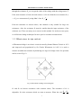
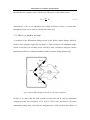
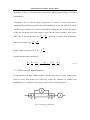
Technical report, IDE1111, October 2011 Setup of pulsed IV system and characterization of magnetic nanocontacts and microwires Master’s Thesis in Microelectronics and photonics Shuo Kong, Xu Sun School of Information Science, Computer and Electrical Engineering Halmstad University ABSTRACT Title: Setup of pulsed IV system and characterization of magnetic nanocontacts and microwires Authors: Shuo Kong, Xu Sun Program: Microelectronics and Photonics ABSTRACT The development of resistance measurement techniques is very important for characterization of future nanoelectronics. Pulsed IV measurement techniques are very useful for accurate resistance measurements on nanoscale samples because of the efficient removal of e.g. EMF errors. In the project we have designed a pulsed IV-setup based on a state-of-the art current source (6221) and nanovoltmeter (2182A) from Keithley, and used the setup for resistance measurements on ferromagnetic samples. Two different samples were investigated using the pulsed IV system – ferromagnetic wires with a central nanoconstriction and amorphous microwires. We have tested the pulse delta system with different pulse widths, duty cycles and voltage levels. The results show a successful integration of the setup. From the measurement results we confirm that the pulse delta system provides accurate measurements with a low noise of about 0.02Ω. The resistance of the samples increases approximately quadratically with bias which is interpreted as a heating effect due to the very high current density of about 107A∙cm-2. KEY WORDS: Low signal measurements, Pulse delta IV measurements, Nanodevices. I Acknowledgements Acknowledgements In this project, we have studied electrical circuit theory, modern measurement technology, and physics. And we have got a good training from the project in innovation and thinking ability. At first we express our gratitude to our supervisor, Håkan Petterson. In the project, his industrious working and nice teaching gave us a strong inspiration. Also, when we have problems, he always provides positive, useful suggestions and encourages us to work continually and efficiently. In the discussion, he always enlightens us with an interesting but very logical way for the measurement planning. Also, we appreciate the other two important teachers Jörgen Carlsson and Lars Landin in the one-year study and researching for their inspiring teaching. At the same time, we give our heartfelt thanks to the university lab and library staff who have offered stable, precise instruments and references which are of great help for our project. Finally, we would particularly like to thank our parents and other intimate friends. Without their love, patience, encouragement and financial support, it would be impossible for us to finish the project. II Scope of the thesis Scope of the thesis At first we learned how to build the pulsed IV delta measurement system from the Keithley 6221 current source and the 2812A nanovoltmeter. Another important part was to establish a useful computer interface to the setup. Then we learned the physics of ferromagnetic nanocontacts and amorphous microwires. Subsequently, we tested the performance and reliability of the pulse delta measurement system by investigating the bias dependence of the resistance of the samples. Finally we carried out some analysis regarding noise properties and heat effects. III Contents Contents ABSTRACT ....................................................................................................................I Acknowledgements ....................................................................................................... II Scope of the thesis ....................................................................................................... III Contents ....................................................................................................................... IV 1 Introduction to resistance measurements .................................................................... 1 1.1 About resistance measurements ........................................................................... 1 1.2 Some technology of resistance measurement ...................................................... 2 1.2.1 Voltage measurements with constant current ................................................ 2 1.2.2 Wheatstone bridge method............................................................................ 3 1.2.3 Kelvin double bridge..................................................................................... 4 1.2.4 Four-point measurements .............................................................................. 5 1.3 Introduction of pulsed IV measurement............................................................... 6 2 Pulsed IV measurements ............................................................................................. 7 2.1 Principles of technique ......................................................................................... 7 2.2 The advantage of this technique......................................................................... 11 IV Contents 2.3 Hardware and connection .................................................................................. 12 2.3.1 Keithley 6221 .............................................................................................. 13 2.3.2 Keithley 2182A ........................................................................................... 15 2.4 The remote control software for computer ........................................................ 17 2.4.1 SCPI control ................................................................................................ 17 2.4.2 The example freeware from Keithley ......................................................... 19 3 Description of samples .............................................................................................. 28 3.1 Basic theory of magnetic nanocontacts .............................................................. 28 3.1.1 Spintronics .................................................................................................. 28 3.1.2 Magnetic domains ....................................................................................... 29 3.1.3 Domain walls .............................................................................................. 29 3.1.4 Spin transfer torque (STT) .......................................................................... 30 3.2 Ferromagnetic nanocontacts .............................................................................. 30 3.3 Amorphous microwires ...................................................................................... 32 4 Measurements and analysis....................................................................................... 34 4.1 The measurement operation ............................................................................... 34 4.1.1 Layout of nanocontact sample .................................................................... 34 V Contents 4.1.2 The mounting,bonding and connection to the measurement system .......... 35 4.1.3 Amorphous metallic wires .......................................................................... 38 4.2 Results and analysis ........................................................................................... 39 4.2.1 Results of resistance measurement ............................................................. 39 4.2.2 Error source analysis ................................................................................... 42 4.2.3 Heat effect analysis ..................................................................................... 45 5 Summary ................................................................................................................... 50 6 Future work and outlook ........................................................................................... 53 References .................................................................................................................... 55 VI Introduction to resistance measurements 1 Introduction to resistance measurements 1.1 About resistance measurements Resistance measurements are rather mature and developed in our modern science world. However, for low resistance measurements, there is still not a fixed model. Low resistance measurements are often associated with semiconductor materials and devices. Because of high conductivity of semiconductor materials and ever decreasing dimensions of devices, low resistance measurements can also be called low voltage measurements. There are many challenges faced by low voltage measurements. Building up a low resistance measurement setup requires choosing compatible high-quality components. The most common instruments include: nanovoltmeter matched up with current source. During the measurements of low resistance nanodevices, error sources can strongly affect the measurement results. In our paper, we have considered many difference error sources. 1) The offset voltage made by thermoelectric effect. 2) Offset made by radio-frequency interference (RFI). 3) Offset made by the selected voltage meter. There are also many noise sources which disturb the measurement accuracy e.g. Johnson noise, shot-noise, magnetic fields and earth loops. 1 Introduction to resistance measurements In our measurements, we used a four-wire method to measure the resistance of the samples, with the purpose of eliminating the influence of contact resistance to the samples. Moreover, to eliminate the offset voltage made by thermal electricity, we adopted pulse-delta mode in our measurement. In the experiment part, we used different samples to check the accuracy of this measurement. The samples are: nanocontacts and amorphous metallic wires. 1.2 Some technology of resistance measurement 1.2.1 Voltage measurements with constant current In Fig.1, we show the principles of this method. It is the basic resistance measure method, which is used extensively in large resistance measurements. r Rt r V I Fig.1-1 Voltage measurements with constant current In Fig.1-1, r is the sum resistance of lead wire and contact, Rt is the resistance to be tested, I is a constant current source, V is a voltage meter with extremely high resistance, so the voltage meter cannot split the current flow in the resistance measurement. First, we know the constant current value I. When the current flows 2 Introduction to resistance measurements through the resistance Rt, we can get the value of the voltage with the voltage meter V. If the sum resistance of lead wire and contact r is far less than the test resistance Rt (r << Rt), we can measure Rt using Ohm’s Law: Rt V . I From the statement we discuss above, this method is only suitable for large test resistances. Also, the resistance Rt must be smaller than the input resistance of the voltmeter too. There are many error sources in this method. So in the next two parts, we will discuss bridge techniques for more precise resistance measurements. 1.2.2 Wheatstone bridge method A Wheatstone bridge is an electric circuit invented by Samuel Hunter Christie in 1833 and improved and popularized by Sir Charles Wheatstone in 1843. It is used to measure an unknown resistance by balancing two legs of a bridge circuit. Its operation can be seen in Fig.1-2. Fig.1-2 Wheatstone’s Bridge Circuit Diagram R1 and R2 are known resistances with constant values, The resistance of Ra is adjustable. Rx is the resistance which we want to measure. When the ratio 3 R1 Ra , R2 Rx Introduction to resistance measurements the null detector (Ampere meter) will be zero. Therefore, at the balance point, Rx ( R2 ) Ra R1 (1-1) Alternatively, if R2 is not adjustable, the voltage difference across or current flow through the meter can be used to calculate the value of Rx. 1.2.3 Kelvin double bridge A variation of the Wheatstone bridge circuit is the Kelvin double bridge, which is used for low resistance (typically less than 0.1 ohm) resistance. Its additional bridge circuit is necessary for avoiding errors caused by stray resistances along the current path between the low-resistance standard and the resistance being measured.[1] Rwire1 Rwire Rwire2 Fig.1-3 Kelvin double bridge (Ra and Rx are low-value resistances) In Fig.1-2, we know that the lead resistance between Ra and Rx may be substantial compared to the low resistances of Ra and Rx. These stray resistances will cause substantial voltage drop, and affect the null detector's value and thus the balance of 4 Introduction to resistance measurements the bridge. In Fig.1-3, the drawback is removed by adding another bridge. A detailed explanation is: Compared to Fig.1-2, the two stray resistances Rwire1 and Rwire2 can be removed by connecting the null detector and RM/RN ratio arms directly across the ends of Ra and Rx. And the stray resistance Rwire can be eliminated by adding the two resistors Rm and Rn so that the left bridge ratio from upper to lower has the same resistance ratio as the other side of the null detector. Set indicate zero and we get Rm RM Adjust Ra, to make the null indicator Rn RN Ra RM Rx RN So the simple equation of Rx is Rx Ra RN RM And the actual balance equation is RN Rn Rx RN Rwire Rm Ra RM Ra Rm Rn Rwire RM Rm (1-2) 1.2.4 Four-point measurements In semiconductor sample characterization, based on the theory above, usually four leads are used. This method can effectively reduce the influence of contacts and connecting wire resistances. The layout is shown in the following figure. Fig.1-4 Four-pole connection 5 Introduction to resistance measurements 1.3 Introduction of pulsed IV measurement In our project, the main task is learning, assembling, exploring and testing a pulsed IV measurement setup. We use the so called pulse delta system to perform pulsed IV measurements on nano- and microdevices from which accurate resistances can be measured. For pulsed IV measurement, there are two solutions which are voltage pulsing and current pulsing. Voltage pulsing produces narrower pulse widths than current pulsing. This makes it more suitable for experiments involving fast thermal transport. High amplitude accuracy and programmable rise and fall times are necessary to control the amount of energy delivered to e.g. a nanoscale device. Voltage pulsing is useful for transient analysis, charge trapping, and AC stress tests during reliability testing, as well as generating clock signals and simulating repeating control lines such as in memory read and write cycles. Current pulsing is very similar to voltage pulsing. In this method, a specified current pulse is applied to the DUT (Device Under Test) and the resulting voltage across the device is measured. Current pulsing is often used to measure very low resistances or to obtain an I-V curve without putting significant power into the DUT that would otherwise damage or destroy a nanoscale device.[2] The pulse delta system that we will study in our Master project, is based on current pulsing technology. We will discuss about it in detail in the next chapter. 6 Pulsed IV measurements 2 Pulsed IV measurements 2.1 Principles of technique The scale of electric devices has become increasingly small. The components made from these devices have increasingly high speed and small volume. However, these small devices do often have strongly limited power managing capacity. When we manage these small devices, we should use small signals to avoid damaging the devices. Pulsed IV measurements offer an accurate low signal measurement solution for nanoscale devices. The so called pulse delta method is based on a current pulsing technique. Here we discuss the current reversal method first: Current reversal method (Delta method) Assume the objective resistance is R0. The thermoelectric emf or voltage (emf: electromotive force) is Vt. The thermoelectric effect mentioned here is generally due to the Peltier–Seebeck effect, that is: a circuit is made from different materials, and the junctions of different materials will act as separate thermocouples. A temperature difference can generate a voltage over the junction which can drive an electric current in a closed circuit. The voltage (Vt) produced is proportional to the temperature difference between the two junctions (in our measurements, the thermocouples will be in the junction between the gold protective layer and the nickel sample, and the junction between the nickel sample and silicon substrate). For typical metals used in thermocouples, the output voltage increases almost linearly with the temperature difference (ΔT).[3] 7 Pulsed IV measurements We know that a constant thermoelectric voltage may be canceled using voltage measurements made at a positive test current and a negative test current. This is called a delta reading. Alternating the test current also increases white noise immunity by increasing the signal-to-noise ratio. A similar technique can be used to compensate for changing thermoelectric voltages (see Fig.2-1). Over the short term, thermoelectric drift may be approximated as a linear function. The difference between consecutive voltage readings (see inset of Figure.2-1) is the slope–the rate of change in thermoelectric voltage. This slope is constant, so it may be canceled by alternating the current source three times to make two delta measurements – one at a negative-going step and one at a positive-going step. In order for the linear approximation to be valid, the current source must alternate quickly and the voltmeter must make accurate voltage measurements within a short time interval. If these conditions are met, the three-step delta technique yields an accurate voltage reading of the intended signal unimpeded by thermoelectric offsets and drifts. Fig.2-1 Thermal voltage plot Here we give another example how the delta method could remove emf error. Let’s assume the temperature is linearly increasing over the short term in such a way that it produces a voltage profile like that shown in Fig.2-2: 8 Pulsed IV measurements Fig.2-2 Voltage measurement with thermoelectric voltage error included. Here we assume Vth = 100nV and is increasing 100nV with each successive reading. The voltages now measured by the voltmeter include error due to the increasing thermoelectric voltage in the circuit; therefore, they are no longer of equal magnitude. However, the absolute difference between the measurements has a constant 100nV error. The first step to remove this error is to calculate the delta voltages. The first delta voltage (Va) is equal to: Va V1 V2 0.95V 2 The second delta voltage (Vb) is made at the positive-going current step and is equal to: Vb V3 V2 1.05V 2 The thermoelectric voltage adds a negative error term in Va and a positive error term in the calculation of Vb. When the thermal drift is a linear function, these error terms are equal in magnitude. Thus, we can cancel the error by taking the average of Va 9 Pulsed IV measurements equal in magnitude. Thus, we can cancel the error by taking the average of Va and Vb: Vf Va Vb 1 V1 V2 V3 V2 100V 2 2 2 2 This is the real value without the influence of thermal error. By using this method, we should choose a measurement system with a short measurement cycle time compared to the thermal time constant which is c pV hAs . Here ρ is density, cp is specific heat V is the body volume, h is heat transfer coefficient, and As is the surface area. The current source must thus alternate quickly in evenly spaced steps, which helps to make a fast measurement cycle time possible. The current step spacing guarantees the measurements are made at consistent intervals so the thermoelectric voltage change remains constant between these measurements. The voltmeter must be tightly synchronized with the current source and capable of making accurate measurements in a short time interval. Otherwise, the arbitrarily change of temperature will cause the change of thermoelectric voltage, thus it cannot reduce the thermoelectricity influence.[4] Pulse Delta Mode The Pulse Delta Mode, derived from the Delta Method discussed above uses a pulsed current instead of a continuous current. The method is illustrated in Fig. 2-3 below: 10 Pulsed IV measurements Assume the objective resistance is R0. The thermal effect of voltage is Vth. The idea here is to measure two voltage values at low current beside the pulse, VI-low 1 and VI-low 2 The reading results are VA VI low 1 Vth and VA VI low 1 Vth . Measure the voltage at high-current, VI-high with the result VB VI high Vth . The correct voltage is given by is Vread 2VB VA VC 2(VI -high Vth ) - (VI -low 1 Vth ) (VI -low 2 Vth ) VI high VI low 2 2 (2-2) VI-high VI-high VI-low1 VI-low2 VI-high VI-low2 VI-low1 VI-low1 VI-low2 Fig.2-3 Pulse Delta Mode structure In Pulse Delta Mode, the three data points received from the voltage meter are moving average values. Even if we only have a couple of data series from one cycle, the noise from this method is lower compared to the Delta Method (Current Reversal Method). Similar to the Current Reversal Method, the system used in the Pulse Delta Mode must allow short measurement times compared to the thermal time constant. 2.2 The advantage of this technique The main advantages with the Pulse Delta Method can be summarized as: 11 Pulsed IV measurements 1) Reduces the Joule heating effects that could potentially damage small nanoscale devices. Joule heating is the process by which the passage of an electric current through a conductor releases heat. Joule heating is caused by interactions between the moving particles that form the current (usually, but not always, electrons) and the atomic ions that make up the body of the conductor. 2) Gives a short response time for the measurement. 3) Any 50/60Hz line frequency noise could be removed by synchronizing the pulse measurement with the line frequency. 2.3 Hardware and connection The Pulse Delta Method studied in this thesis is built from two high-end instruments from Keithley - the current source 6221 and the nanovoltmeter 2182A. First we should acquire some basic knowledge of the two instruments. One of the best advantages of 6221 and 2182A is that they are equipped with an interface with trigger link for convenient setup of a pulse delta measurement system. In pulse delta mode, the Model 6221 provides a bipolar output current and the Model 2182A performs A/D conversions (measurements) at source high and source low points. A built-in averaging algorithm is then used to calculate the delta reading.[5] Why do we use a current source and not a voltage source? Of course, every power source could feed current to devices, but most of them can only tune the output voltage and therefore the current will depend on the load resistance. In many cases, e.g. if the load resistance is very small, it is better to use a current source. 12 Pulsed IV measurements 2.3.1 Keithley 6221 Keithley 6221 is a precise current source with very low current noise. Low current sourcing is critical to applications in test environments ranging from R&D to production, especially in the semiconductor, nanotechnology, and superconductor industries.[6] Fig.2-4 Keithley 6221 The main features of K6221[7] are: 1) Source and sink 100fA to 100mA, Source AC currents from 4pA to 210mA peak to peak for AC characterization of components and materials 2) 1014Ω output impedance 3) 65000 point source memory 4) Built-in RS-232, GPIB, Trigger Link, digital I/O and Ethernet interfaces. Built in standard and arbitrary waveform generators with 1mHz to 100kHz frequency range 5) Reconfigurable triax output 6) Programmable pulse widths from 50μs to 12ms when used with model 2182A 13 Pulsed IV measurements Nanovoltameter The applications of K6221[8] include: 1) Nanotechnology: Differential conductance. Pulsed sourcing and resistance measurements 2) Optoelectronics: Pulsed I-V 3) Replacement for AC resistance bridges (when used with Model2182A): Measuring resistance with low power 4) Replacement for lock-in amplifiers (when used with Model2182A): Measuring resistance with low noise In our project, the K6221 is connected to the 2182A to form the Pulse Delta setup. The K6221 acts as a source for output sweep function amplitude pulsed current. Also, we use the normal DC current mode for testing and calibration purposes. There are two ways to control the K6221. Firstly, for basic use, we could just control it from the front panel. For more advanced resistance measurements, we use a computer to control the instrument. For the common computer control, SCPI (Standard Commands for Programmable Instrumentation) is needed. Just set up the Keithley I/O Layer software (including Keithley configuration panel and wizard, communicator, visa runtime and SCPI-based instrument driver). Then select the right matched interface (only the Ethernet port is available to use because we use the laptop). At last just set the right parameter and create the new virtual instruments, and we could input the command in the communicator to control the K6221. 14 Pulsed IV measurements There is another easy and convenient way of controlling the K6221 by a computer. The free example software based on Labview language can be downloaded from Keithley´s website. By this software we could just use the virtual panel and GUI parameter option to configure the instrument. 2.3.2 Keithley 2182A The Keithley 2182A is a two-channel, high definition nanovoltmeter for low voltage measurements. The 2182A is a good companion to the 6221.They can be connected together as a pulse current measurement system. It is optimized for making stable, low noise voltage measurements and for characterizing low resistance materials and devices. It provides higher measurement speed and significantly better noise performance than alternative low voltage measurement solutions.[9] Fig.2-5 Keithley 2812A The main features of 2812A[10] are: 1) Low noise measurements at high speeds, only 15nV p-p noise at 1s response time, 40–50nV p-p noise at 60ms 15 Pulsed IV measurements 2) Delta mode measurements with a reversing current source at up to 24Hz with 30nV p-p noise (typical) for one reading. This kind of averages multiple readings for greater noise reduction 3) Synchronization to line provides 110dB NMRR and minimizes the effect of AC common-mode currents 4) Two channels support measuring voltage, temperature, or the ratio of an unknown resistance to a reference resistor 5) Built-in thermocouple linearization and cold junction compensation The applications of 2812A include[11]: 1. Research: 1) Determining the transition temperature of superconductive materials 2) I-V characterization of a material at a specific temperature 3) Calorimetry 2. Metrology 1) Intercomparisons of standard cells 2) Null meter for resistance bridge measurements In the present pulse delta setup, the 2182A is used to measure the voltage, and to perform A/D conversions, at source pulse high and pulse low points. We connect the 2182A to the K6221 with RS-232 cable and trigger link cable. The communication between the two instruments is based on RS-232 interface. The trigger link cable synchronizes triggering between the two instruments. Here 2182A should use the default setting for the connection: 16 Pulsed IV measurements 1) EXT TRIG (input) = line #2 2) VMC (output) = line #1 2.4 The remote control software for computer There are two basic ways to control the instruments from a computer. The first and basic method is via the SCPI language. The other way is to use the freeware based on Labview offered by Keithley. 2.4.1 SCPI control SCPI is Standard Commands for Programmable Instruments. It defines a standard for syntax and commands to use in controlling programmable test and measurement devices. The SCPI standard defines the basic command structure and syntax used in programmable instruments through a communication interface. For now there are GPIB, RS-232, USB, VXIbus etc. Also, SCPI contains the standard common command tier for different types of programmable instruments, such as power sources, current- and voltmeters and oscilloscopes. Of course, the SCPI does not define the physical method of communication. As originally developed for GPIB (IEEE488.2)-based equipment, SCPI is now also used for communication via RS232, USB, LAN connections and other interfaces.[12] There are some steps in the preparation for the communication link: 1. To enable the SCPI control of the instruments, we need the necessary driver and software to offer the communication between the instruments and the computers. Here we use Windows 7 professional as the platform. 17 Pulsed IV measurements 2. Download “KIOL Layers” and install it. 3. The I/O Layer is designed to be installed and to work seamlessly with instrument drivers provided by Keithley Instruments for Keithley's test and measurement equipment. 4. Configuration panel and wizard: Most common operations can be performed using the Wizard, while the Configuration Panel provides additional capabilities needed for some special situations. 5. Commuicator: The communicator lists only resources saved in the IVI and NI-VISA configuration data files. So it won’t auto-detect USB or other devices. [13] After the preparation, we could set the remote interface. Here for K6221, the available interfaces with computers are GPIB, RS-232, and Ethernet. Since the computer we use is a laptop, we just use the Ethernet interface. For the Ethernet interface, the user must set the matched IP address, gateway and subnet mask when DHCP server isn’t used. And the MAC address is fixed and can’t be changed (also we don’t need to change it). With Ethernet interface, only the SPCI language could be used for the control of the instruments (KI-220 DDC language is not supported). The settings we use are: Computer IP: 192.168.0.2 Instruments IP: 192.168.0.3 Subnet mask: 255.255.255.0 Gateway: 192.168.0.1 18 Pulsed IV measurements 2.4.2 The example freeware from Keithley Though SCPI control is the main and basic method to control and communicate with the instruments from computer, it is complex for the junior user who just begins to use the instruments. So Keithley offers example software for the users who use K6221 (and the pulse measurement system includes 2182A). The program is easy to use. It is working in GUI (Graphical User Interface) mode. Due to the benefits brought by GUI operation, the user could control K6220/6221 (and 2182A when in the delta mode or pulse measurement mode) from a computer just by clicking to change the parameter of the preset program and then run it or use the virtual front panel (similar to the real instrument front panel). Most functions of the instruments could be operated from the example software, such as to perform delta mode, differential conductance, pulsed IV measurements, and to output arbitrary waveforms. Preparation for the software: 1) First access the same download page to download the example software, and VISA 3.01runtime. 2) Setup VISA3.01 at first. It is necessary for the example software. 3) Run the setup.exe file in the documents of example software. 4) After the setup, configure the basic connection and ready to use. Introduction of VISA and Instrument driver VISA represents Virtual Instrument Software Architecture. It is a widely used I/O API in the Test & Measurement industry for communicating with instruments from computer. VISA is an industry standard implemented by several T&M companies.[14] 19 Pulsed IV measurements An Instrument Driver, in the context of Test & Measurement (T&M) application development, is a set of software routines, which simplifies remote instrument control. The specification of instrument drivers is defined by the IVI Foundation. An instrument driver is usually characterized by a well-defined API.[15] The example software is based on Labview 7. It is a set of various VIs (Virtual Instrument). For each VI, there are three components: a block diagram, a front panel, and a connector panel. The front panel is important for users. Controls and indicators on the front panel allow an operator to input data or extract data from a running virtual instrument. Also the front panel can serve as a programmable interface or just a node in the block diagram. The example software is a product of the G language, as the dataflow programming language. It is very convenient for the non-programmers to build and test the VIs set program. Configure of the example software: Start the program from the shortcut on the desktop or the start menu. Open the program window. 20 Pulsed IV measurements Fig.2-6 Main window of example software This is the main window of the K6220 example software. Firstly, we should check the “Step-by-Step Connection Guide” to confirm whether the connection is right or not. After the check, click “FINISH” and go back to the startup screen. Then click “Setup Wizard”, enter the Wizard to guide the configuration of your system. Fig.2-7 Setup wizard Here the current source is 6221 and the nanovoltmeter is 2182A. The interface we use is the Ethernet port with the IP address mentioned before. Since the figure is screened in the unconnected condition, “VERIFICATION FAILED” is showed. Because the measurements that we will do are low voltage measurements, the source connection setting should be “UNGUARED SOURCING”. For the measurement connection, “4-WIRE CONNECTIONS” is chosen to remove any contact resistances. At last we choose “NO EARTH CONNECTION” and “INPUT OPERATION” for the most common situations. 21 Pulsed IV measurements We could use the virtual front panel for most simple operation and configuration of the instruments. Of course, for some simple operation and configuration, it is more convenient to operate on the real front panel of the instruments. There is a time lag in the communication between the instruments and computer. Check on the “Take control of Instrument” box will enable the control from computer. In the bottom the user could send the SCPI command directly to the instruments to make the control more comprehensive. Fig.2-8 Virtual Instrument Front Panel The most important function we will use is the pulsed IV measurements. Click “Advanced Operation” tab and the sub tab of “Pulsed IV Measurements”. 22 Pulsed IV measurements Fig.2-9 The tab of Pulsed measurements Click “GRAPH” to plot the data in the graph. In the tab zoom and compare etc. functions are included too. In the top of each measurement function, there is a “GENERATE SCPI” button. The user could get the corresponding SCPI command code of the GUI control. Most parameters are in the three tabs: “SETUP”, “TIMING”, “ADVANCED”. Here follows a brief introduction. Pulse mode: two choices, repeat pulse amplitude, and sweep pulse amplitude. For Repeat pulse amplitude, the K6221 current source will generate a fixed output sequence during every Pulse Delta cycle as shown in Figure 2-8 below. The pulse width is adjustable and is the same for all high and low pulses. 23 Pulsed IV measurements Fig 2-10 Repeat pulse amplitude mode For Sweep Pulse Amplitude, the K6221 can output a series of pulses with different amplitude for the high pulses (see Fig. 2-11 below). Each high pulse returns to the programmed low pulse level which is the same for all the pulses. There are 3 types of sweep output pulses: Staircase sweep, Logarithmic sweep and Custom sweep. Fig.2-11 Staircase sweep, Logarithmic sweep and Custom sweep 24 Pulsed IV measurements In our measurements, we will use the Sweep Pulse Amplitude since we want to measure the resistance trend for increasing current. Start pulse level and stop pulse level: the two parameters will decide the minimum and maximum current amplitude of the pulse. For most time, we will set the start pulse level to zero. Number of pulses: This parameter will decide how many pulses will be generated in the measurement progress. Using more pulses will make the measurement time longer. Sweep type: As we described above, there are two types of sweeps: linear and logarithmic. Voltage measure range: Here just choose the desired range of maximum and minimum voltage for the measurement. In “TIMING” tab: Pulse width: This is an important parameter. The range is from 0.05ms to 12ms. Long pulses will bring a similar effect like DC current. Delay – pulse settle time: The delay is different from the sweep delay that defines the pulse delta cycle time period. It is used to allow the pulse to settle before triggering 2812A to start a measurement conversion. The source delay could be from 16μs to 11.966ms. Both pulse width and source delay will determine the integration rate or measurement speed of the model 2182A. Interval between pulses: For most time 5PLC is ok. 25 Pulsed IV measurements For 60Hz line power: the pulse delta cycle time period = PLC * 16.667ms For 50Hz line power: the pulse delta cycle time period = PLC* 20ms We use 50Hz line power, so the time period is 100ms. In “ADVANCED” tab: Current source voltage compliance: It is the maximum voltage safety limit generated by the current source. For most time it is set to 10V. For most low level measurements, it is rarely that the voltage is larger than 10V. Pulse off level: It is the current value when the pulse is off. For most time it should be zero. Number of pulse measurements: Typically, the pulse delta technique uses a 3-point repeating algorithm to calculate readings. Each pulse delta reading is calculated by using A/D measurements for a low pulse, a high pulse, and another low pulse. But sometimes when the high pulse will cause heating of the device under test, the measurement at the second low pulse could be seriously affected by the heat caused by the high pulse. So in this case we will abandon the measurement at the second low pulse. There are the other 3 tabs in the right side of the “ADVANCED” tab, they are labeled “GRAPH” , “SHEET” and “HELP”. The “GRAPH” tab will plot data points, such as voltage versus points/current/time automatically. Also the zoom and compare functions are contained in the tab. The “SHEET” tab is the record of the digital data points. As we have mentioned, the result could be saved but in KDF.files. In fact, the KDF file is a type of text file, but 26 Pulsed IV measurements when the files are saved in Windows, they can’t be opened by Word or Excel instantly. The solution is to right click the files and select Excel in the application program menu. To analyze the data, the KDF should be converted to XLS the formal EXCEL files. 27 Description of samples 3 Description of samples 3.1 Basic theory of magnetic nanocontacts Current-induced magnetization switching in magnetic multilayers is a new technology for data storage and reading.[16] This technology can be successfully explained by the spin transfer torque effect.[17] To make a better understanding of our samples, the following theory is necessary to be introduced first. 3.1.1 Spintronics Spintronics is the abbreviation of "spin transport electronics".[18] It is a technology that exploits the properties of both the intrinsic spin (magnetic moment) of electrons and the more conventional charge.[19] The information technology is making great progress due to the development of new semiconductor and ferromagnetic materials. As we know, electrons carry both charge and spin properties. Using the charge property, microelectronics has become the basics of all information communication and computation. Using the electron spin forms a new technology of modern information storage, like MRAM. In the 1980s, Johnson first realized spin injection into ferromagnetic, metal and ferromagnetic (FeNi/Cu/FeNi) sandwich structures.[20] 28 Description of samples 3.1.2 Magnetic domains A magnetic domain describes a region within a magnetic material which has uniform magnetization. This means that the individual magnetic moments of the atoms are aligned with one another point in the same direction due to an “exchange coupling”. Magnetic domain structures are responsible for the magnetic behavior of ferromagnetic materials like iron. In a non-magnetized ferromagnetic material, the domains will have random magnetic directions and thus there will be no macroscopical magnetism. In a magnetized ferromagnetic material, the domains have the same magnetic direction, and thus a macroscopic magnetic moment. 3.1.3 Domain walls In magnetic materials, a domain wall is an interface separating magnetic domains. It is a transition between different magnetic moments and usually undergoes an angular displacement of 90 or 180 angles. On average, the thickness of a domain wall is around 100-150 atoms. Non-magnetic inclusions in the volume of a ferromagnetic material, or dislocations in crystallographic structure, can cause "pinning" of the domain walls. Such pinning sites caused the domain wall to seat in a local energy minimum. And to "unpin" the domain wall from its pinned position, external field is required. The act of unpinning will cause sudden movement of the domain wall and sudden change of the volume of both neighboring domains. When an external field is added, the magnetic moments turn to the direction of the field, thus the total magnetic torques will increase. Finally, all the magnetic torques will have a same direction, and the magnetic torques will be to the maximum. Though the directions of magnetic torques are the same, there are still some differences between the direction of magnetization and field. When the field is keeping on increasing, all the directions will be the same, and this process is called 29 Description of samples "saturation".[21] The magnetization of a ferromagnetic material is dependent on temperature. As the temperature increases, the ferromagnetic coupling will be overcome by the thermal energy leading to paramagnetism. This transition temperature is called the Curie temperature. 3.1.4 Spin transfer torque (STT) Spin Transfer Torque is a mechanism to reorient the magnetization of a thin magnetic layer in a magnetic multi-layer device e.g. a tunnel magnetoresistance (TMR) element using a spin-polarized current. In non-ferromagnetic samples, the spins of electrons are usually randomly oriented, thus they do not show any special direction totally. However, when the current is going through a ferromagnetic sample, the electrons become partially spin polarized and these spin can play an important role. A flow of spin polarized electrons can influence the macroscopic magnetization direction of e.g. a thin magnetic layer. This effect, called spin transfer torque, forms the basis of many new types of spintronic devices. Already in the late 1970s and 1980s, Berger predicted that a spin transfer torque should be able to move magnetic domain walls.[22] His group observed the domain wall motion under the influence of large current pulses.[23] In 21st century, spin-transfer-induced domain wall motion has been made a huge development by many groups.[24] 3.2 Ferromagnetic nanocontacts We can use a thin ferromagnetic wire patterned with a nanoconstriction to trap a 30 Description of samples domain wall in Fig.3-1. By changing the current through the nanoconstriction, the domain wall is unpinned from the constriction by current induced domain wall motion at a critical current value which is depended on the material. The creation and vanishing of the domain wall in the nanoconstriction will cause a resistance change. The current induced magnetic switching has been predicted theoretically by Berger and verified experimentally.[25] Using applied current pulses to make the displacement of domain walls has been demonstrated by Gan et al.[26] It was found that current densities of the order 107 A/cm2 are required to displace a domain wall. By pinning a domain wall in a nanoconstriction and suddenly removing it with increasing current, there will be a sharp change of resistance (MR) in the material. The first goal of this thesis is to investigate this effect by studying the resistance versus current density in ferromagnetic nanowires with a central nanoconstriction that acts as a pinning site for domain walls. The devices are shown in Fig. 3-1 below. The nanocontact structures of ferromagnetic metals with different magnetic coercive forces were fabricated by electron-beam lithography (EBL) and lift-off techniques on SiO2/Si. Subsequently about a 30 nm-thick ferromagnetic metal layer (such as Fe, FeNi, Ni or Co, in our measurement we use sample pad #16, the sample material is pure nickel ) was deposited by a radio frequency magnetic sputtering method in Ar and about 2 nm thick Au capping layer was deposited on the ferromagnetic metal layer to prevent it from oxidation.[27] 31 Description of samples Nanoconstriction Fig.3-1 Pattern of nanocontact. Right figure shows nanoconstriction. 3.3 Amorphous microwires Amorphous materials are non-crystalline materials. If the molten alloy is cooled rapidly, the structure after solidification presents the state of glass. Amorphous materials have many excellent properties such as high strength, high toughness, excellent magnetic properties and corrosion resistance. Amorphous material is widely used and these materials can be made in a variety of shapes, such as films, ribbons, wires, powders. In particular, amorphous wires have attracted a lot of interest from industry due to their potential applications in electronic systems. The second goal with this Master project is to measure the resistance of amorphous microwires for different current densities.[28] During the process of magnetization in longitudinal direction, the length of amorphous wires will change and the magnitude can be expressed as magnetostriction coefficient λ. If the length increases, the wires are called positive magnetostrictive materials such as Fe-based amorphous wires. If the length decreases, the wires are called negative magnetostrictive materials such as Co-based amorphous wires. Feand Co-based amorphous wires are very important amorphous metallic materials, because they have their special electromagnetic properties. In our measurement, we 32 Description of samples use Co-based amorphous wire. Fig.3-2 Schematic representation of an amorphous glass-covered metallic wire 33 Measurements and analysis 4 Measurements and analysis 4.1 The measurement operation In the last chapter we will introduce the basic information of the measurement system and the operation of the software for the instruments and we will test and learn how to use the system and do some basic measurement on the samples that we have introduced before. 4.1.1 Layout of nanocontact sample First we investigated the layout of the sample with a high-resolution optical microscope (Zeiss Axioimager M2). Fig4-1 and 4-2 show microscope images of the sample at high and low magnification, respectively. Fig.4-1 Microscope image of sample at high magnification 34 Measurements and analysis Fig.4-2 Sample at low magnification As we can see from the pictures above, there are four thin contacts made of gold connected to the wire, which makes it possible to make 4-point measurements previously discussed. The thin contacts are terminated with bonding pads where bonding wires are attached to the sample holder. Alternatively, the bond pads can be used directly for measuring the resistance with a probe station. 4.1.2 The mounting,bonding and connection to the measurement system There are two ways to connect the sample to the pulse measurement system. The most robust way is to use a sample holder and the bonding machine. Here give a detailed 35 Measurements and analysis introduction: 1) Use glue to make the sample stick together with the sample holder (Fig. 4-4). 2) Put the sample holder (with the sample glued to the holder) on the heating pad of the bonding machine (see figure below). Set the bonding parameters. Here we used bonding wires made of gold. Fig.4-3 The bonding machine 3) When the heating pad was 60°C, the bonding process could start. Gold wires were bonded to each of the four bond pads connecting them to large contacts on the sample holder. 4) The sample holder was inserted into a bread board to allow proper contact between the instruments and sample holder (Fig.4-5). The step is easier than the last step, and it is enough to use normal jump wires to connect the board. 5) The last step is to that connect the bread board to the pulse measurement system. 36 Measurements and analysis Fig. 4-4 The sample mounted on the sample holder Fig.4-5 The sample holder on the bread board Fig.4-6 The whole pulse measurement system The second way to connect samples to the pulsed IV setup is to use a probe station with thin probe needles directly touching the bond pads of the sample. We have tested this method at Lund university. Here is the introduction. 1) Put the sample (the sample holder isn’t needed in this method) in the central pad of the probe station. Then close the chamber of the probe station. 37 Measurements and analysis 2) Connect the probe cable with the instruments. There are four cables for the current source and voltage meter, as in the first method. Tune the probes and make them firmly touch the bond pads on the sample. As the connection is finished, we could start the measurement by starting the computer and the pulse delta system. 4.1.3 Amorphous metallic wires Amorphous metallic wires are relative new materials which have attracted a lot of interest for basic research and potential applications in microwave components. These wires have an interesting magnetic behavior which originates from their special magnetic domain structure due to the stress difference between the surface and center. Here the measurement preparation for the wires. The Co-based wires are some micrometers in diameter and about 30-50 centimeters long. 1) First we should cut the wires into a suitable length with a special knife. 2) Then use the rough sandpaper or the knife to remove the glass coating which protects the central part. Here only the glass coating at the ends of the wire needs to be removed. 3) Prepare the soldering iron and heat it. To mount the wire on the sample holder (a microstrip), we solder the ends of the wire to the connectors on the copper microstrip. Here we must be very careful, the solder paste must be small due to that it may short circuit the connector if the solder paste is large. 4) At last soldering two jump wires on the connector as the new connector. 38 Measurements and analysis Fig.4-7 The microwire on the microstrip After this preparation, the resistance measurement of the microwires could be started using the pulse delta setup. 4.2 Results and analysis 4.2.1 Results of resistance measurement In this section we will discuss the results from the resistance measurements on ferromagnetic nanocontacts and amorphous microwires described in the previous chapter. We choose Dataplot and Matlab to plot the experimental data presented in the figures below. At first, we use Dataplot to plot the basic and single data paste from Excel files. It is convenient for the single function plot and the grip setting. But for the multivariable plot, it is more instant and convenient to use Matlab. With Matlab, we just need to import the excel files from the Workspace window of Matlab. 39 Measurements and analysis Fig.4-8 Resistance of nanocontact sample measured with our pulse delta mode setup (No.8 device on sample pad #16, pulse width between 2ms-12ms, 500 measurement points for each measurement, Source Delay 0.1ms, Voltmeter range 1V) 40 Measurements and analysis Fig.4-9 Resistance of nanocontact sample measured with pulse delta mode setup (No.16 device on sample pad #16, pulse width between 2ms-12ms, 600 measurement points for each measurement, Source Delay 0.1ms, Voltmeter range 1V) 41 Measurements and analysis Fig.4-10 Resistance of nanocontact sample measured in constant current mode (No.16 device on sample pad #16) Fig.4-11 Microwire measurement with pulse delta method 4.2.2 Error source analysis As we have mentioned in chapter 1, there are many error sources existing in resistance measurement results. The main error sources are Johnson noise, external noise source, thermoelectric voltages, test lead resistance and 1/f noise. For Johnson noise, it is a fundamental limit on resistance measurement. It is mainly due to the random motion of charged particles. It has a white noise spectrum, which is related to the resistance, temperature and frequency bandwidth values. It is given by 42 Measurements and analysis VJohnson rms 4kTRB (4-1) Here, k=Boltzmann’s constant, T=absolute temperature in K, R=DUT resistance in Ohms, B= noise bandwidth in Hz. Assume the temperature is 290K, resistance is 30 Ohm and the noise bandwidth is 13Hz. The Johnson noise amounts to about 0.02μV. For external noise source, it is mainly due to the devices related to the measurement equipment and grounding issues. The noise could be decreased by shielding, filtering and cut off the noise source. Due to that these external noise are most at the power line frequency, in our measurement, we could minimize these noise partly by integrating each measurement for an integer number of power line cycles. Thermoelectric voltages can be partly eliminated by current inversing method (Delta Mode) as we have mentioned before. To remove test lead resistances we have used four-wire measurement (Kelvin) configuration to measure. 1/f noise, usually is used to describe all the noise which is increasing magnitude at lower frequencies. This noise could be observed as many aspects, such as a current, voltage, temperature, or resistance fluctuation. And this noise is caused by many environmental factors as temperature or chemical processes in components.[29] From the discussion above we know that the major noise source in the results is thermoelectric voltage and 1/f noise. The figures above show the results of our measurement. In Fig.4-8, we display the result for No.8 device on sample pad #16 in pulse delta mode. We know that, the Johnson noise is about 0.02μV, and the noise resistance can be calculated by dividing the current. We can see the noise resistance contributed by Johnson noise is really small compared to the other two major noise sources. And in the result, we could see the resistance noise value will decrease as the 43 Measurements and analysis current increases. In the low current region, there is indeed a relatively large resistance noise due to the thermal voltage (though some of this noise could be extinguished by delta or DC current reversal method, the remove of this noise also is dependent on the similarity of the characteristic of the material of the contact junction in the circuit). Fig.4-9 shows another device (No.16) on sample pad #16 measurement. And for the small resistance fluctuation in the result, we could know it is belong to common 1/f noise by check nanotechnology measurement handbook published by Keithley, Again the data is taken with the pulse delta mode. We can see that the noise is decreasing with increasing current. Fig.4-10 shows the result that the resistance versus current for No.16 device on the sample pad #16 in DC current mode. In this measurement, the thermal electric error is expected to be present since the data is measured under DC conditions. We can see clearly compared with Fig.4-9 above, that the noise is larger in DC current measurements due to thermal electric error. From Fig.4-8 and Fig.4-9, the resistance noise we can get is about 0.02Ω. In Fig.4-10, the total noise is about 0.04Ω, which is almost twice compared with the result got from pulse delta mode. The result is acceptable and reasonable. Fig.4-11 shows the resistance data obtained from pulse delta measurements on an amorphous microwire. Due to the lack of time, we didn’t test it in DC current mode. Due to that the diameter of this wire is much larger than the nanocontact, it makes the cross section area and the whole volume (also the microwire is rather longer than the nanowire) much larger than the nanowire. These facts could give the microwire better heat conducting properties. In addition, the protective glass layer around the microwire makes this sample more stable that the cobolt nanocontact samples which suffered from oxidation problems. All of these reasons contribute to the result that the 44 Measurements and analysis increase of the resistance and noise is really low for the amorphous microwires. 4.2.3 Heat effect analysis As seen in all the experimental data, the resistance increases with current (both DC and pulsed). At first, we calculate the current density through the nanocontact: For Fig.4-8, the width of No.8 nanocontact on sample pad #16 is 150nm, and the thickness is 30nm. So the cross section area of the nanocontact is 4.5×10⁻¹¹cm2 (150nm×30nm). The material of the sample is nickel. And the range of the current pulse is from 0mA to 1.5mA. So the range of current density (current/area) is 0 to 3.33×10⁷A∙cm-2 and we could see from the figure that the heating effect is noticeably when the current is increasing to 0.5mA, here the current density is 1.11×10⁷A∙cm-2. For Fig.4-9 No.16 nanocontact, the width of No.16 nanocontact is 560nm, the thickness is the same as No.8 device. So the cross section area is 1.68×10⁻¹⁰cm2. The range of the pulse current is from 0 to 2.5mA. And the current density is from 0 to 1.49×10⁷A∙cm-2. Also we could see an obvious heating effect when the current is increasing to 0.5mA, and the current density is 2.98×10⁶A∙cm-2. Now we could see even when the current is small for the nanocontact, the current density which is going through the nanocontact is really large due to the small cross section area. Also even when the pulse width is only in the millisecond magnitude, the heat effect is still important. Metals contain a lattice of atoms, each with a shell of electrons. The outer electrons are free to dissociate from the atoms and travel through the lattice forming an “electron sea”. This is why the resistance of metals is so small. Near room temperature, the thermal vibration of lattice ions is the primary source of scattering of 45 Measurements and analysis electrons. When the temperature increases, the thermal vibration of ions will also be enhanced causing an increase of resistance. That actual raised temperature of the sample can be calculated by using the temperature coefficient of resistivity of the material using this formula: R T R T0 [1 T ] (4-2) T0 is the reference temperature (Here in our lab, the reference temperature is 20℃), and ΔT is the difference between T and T0. R(T) is the resistance at temperature T. R(T0) is the resistance when the temperature is the reference temperature (typically room temperature). Finally, α is the (linear) temperature coefficient. α= 0.005866 for nickel, at 20℃. For nanocontact No.8, R(T0)=36Ω (pulse width is 8ms), R(T)=36.1Ω (pulse width is 8ms). So we could calculate ΔT=0.474℃ from egn. 4-2. For nanocontact No.16, R(T0)=57.8Ω (pulse width is 8ms), R(T)=58.4Ω (pulse width is 8ms). We could calculate ΔT=1.770℃. And based on the heat conduction equation and the generating Joule heating, we could explore the heat conduction and calculate the temperature gradient. The energy generated by the current (Joule heating) can be written as E I 2 Rt At first, we could assume the sample is thermally isolated from the surroundings. The parameters of nanocontact No.8 is: 46 (4-3) Measurements and analysis Thickness=30nm, Length=100um, Width=1um, Density=8908 kg/m3(Nickel), m=2.6724×10⁻¹⁴kg (the mass of the sample), c=440Jkg-1℃-1 (specific heat capacity of nickel), R=36Ω, I=0.75mA (use the average value), Δt(pulse width multiplies the number of measurement points)=8ms×500points=4s. So the temperature change can be written as Tmc I 2 Rt 8.1105 J T I 2 Rt 6.9 106℃ mc (4-4) (4-5) So we could see the temperature change is extremely large. This assumption is obviously unreasonable, and heat conduction must be taken into account. Simulating heat conduction in these nanosystems is, however, beyond the scope of the thesis. We note from the equations 4-2 to 4-6 above that the resistance is expected to change quadratically with current and linear with the pulse width. Here we use MATLAB to do some curve fitting for the result. For nanocontact No.8, we use the curve of width 8ms. 47 Measurements and analysis Fig.4-12 Curve fitting for No.8 nanocontact(pulse width 8ms) The typical quadratic dependence of the resistance with current is indeed shown in Fig. 4-12 above. The equation of resistance versus current is: R 4.253e+004 * I 2 0.986 * I 35.99 For No.16 nanocontact, we also use the curve of width 8ms. Fig.4-13 Curve fitting for No.16 nanocontact(pulse width 8ms) We could get the approximate equation from the curve fitting, here we use quadratic polynomial type to get the fitting. And the equation of resistance versus current is: R 1.682e+005 * I 2 -232.2 * I 57.94 Fig.4-14 below shows the resistance versus pulse width An approximate linear dependence is observed in line with the arguments above. 48 Measurements and analysis Fig.4-14 Resistance versus pulse width with fix current density(1.11 × 10⁷A∙cm-2, 2.22 × 10⁷A∙cm-2, 3.33×10⁷A∙cm-2) (No.8 device on sample pad #16, pulse width between 4ms-10ms, Source Delay 0.1ms, Voltmeter range 1V) 49 Summary 5 Summary During the preparation of this thesis work, we made a plan, looked for references, and learned the user manual of the pulse delta system. After the theory study, we entered the practice process: to combine the two instruments to a pulse delta system, to test the system with a well-known reference resistor, and finally to use the setup for studying ferromagnetic nanocontacts and amorphous microwires. We had severe problems in the process and many of the ferromagnetic contacts were destroyed during the measurements. There are three parts in this project, and in the following we will summarize what we have learned from the whole project. The topic of the project is completely new to us. In the first part, we learned how to use the very sophisticated instruments from Keithley. So it was necessary for us to get the user and reference manuals, the matched drivers and software. The two instruments were combined into the pulse measurement system. From the manual we could get the proper parameter settings, the basic operation and the explanation about pulse measurement method. The second part was to study the complex physical properties of the samples to be investigated. There are two types of samples for the measurement: nanocontacts and microwires. The third part is the measurement part. In our measurements we use the Keithley 6221 and Keithley 2812A combined together as a pulse delta measurement system. We also used a third instrument, the Keithley 2602, for DC measurements. From the result we could observe that the noise error in DC measurement is larger than the noise error in 50 Summary pulse delta measurement. After the measurements, we have analyzed the results: 1. Noise error source analysis: 1) At first we discussed the main noise source in the measurement, and found that Johnson noise is the major noise source that makes the largest effect on the measurements. 2) Then we compared the results from pulse delta mode measurements with the result from normal DC current measurements and found that the noise is reduced by the pulse delta technique. 3) For the microwire measurements, the larger volume and cross section area combined with the protect layer of the microwire makes the measurements of this sample more stable. 2. Heat effect analysis: We have analyzed the dependence of the resistance on the current pulse amplitude, and pulse width. The current density through these samples is extremely high due to their small dimensions. We conclude that Joule heating provides the source for the increase of resistance with increasing pulse width. We found that the resistance increases quadratically with pulse amplitude and linearly with pulse duration in agreement with a simple model for Joule heating. We also found that there is a very effective heat conduction from the samples to the surrounding, without which the samples would immediately be destroyed by the heating. In the project we encountered many problems, but finally we have solved most of them successfully: At the beginning, the mounting and the connection of the samples were problematic. 51 Summary Two different techniques were used: bonding machine and probe station. Another problem was data communication between instruments and control computer. Here we choose the Ethernet port as the communication interface. For the communication interface, we chose the example software rather than the SCPI language to use computer to control the system. As we have mentioned before, the software is somehow old for the latest operation system (Windows Vista/7), so we used virtual machine software on the operation system, and setup Windows XP on the virtual machine to solve the problem. Another problem is the date collection. The data received from the software is KDF files that could be opened by Microsoft Office Excel, but it is not a formal file type for Excel. We thus had to convert the KDF files to XLS, the formal Excel files. Datafit and Matlab were finally used to analyse and plot the data imported from Excel. However, there are still some problems that we couldn’t solve , due to the lack of knowledge and time. In the next section on future work we will discuss some of them. 52 Future work and outlook 6 Future work and outlook In the project we have learnt that the setup of the driver and software for the instruments are too complicated to be used conveniently for the basic software users. The setup of the driver and software package must be simplified. We have also found that the example software for the instruments did not work properly in Windows 6.X(Vista/7). The software could be set up and started, but when we finished using it and want to close down, the system crashed leading to an abrupt restart which is harmful for the computer hardware. Up to now, our solution is to use a virtual machine software to set up Windows XP. In the future, we should use the new version of Labview to change and update the VI(virtual instruments) of the example software to make it compatible to Windows 6.X(Vista/7). In the project, we also suffered from a breakdown problem of the samples. Burnt part Burnt part Fig.6-1 Electron microscope image of a burnt sample 53 Future work and outlook This problem, shown in the Zeiss Axioimager M2 image of Fig. 6-1, only occurred for the nanocontact sample and not for the microwire. Up till now, we have no clear idea what the problem was. Most likely, it is connected to a static electric discharge. In the future, we will continue to explore the reason for this breakdown. To sum up, we have learnt in this project how to find useful references and how to work on low signal measurement instruments. We have built an advanced pulsed IV measurement unit and used it to characterize important micro- and nanoscale devices. We have also received training in noise and data analyses. Altogether, the project was a nice training for our ability of think independently and innovative. The knowledge we have got from the project is very useful and important for our future study and research. 54 References References [1] All About Circuits. Bridge circuits introduction. http://www.allaboutcircuits.com/vol_1/chpt_8/10.html, 2010. [2] Jonathan Tucker. Pulse Testing for Nanoscale Devices. Keithley Instruments, Inc. May 2007: P1. [3] Wikipedia. Biography of Seebeck. http://en.wikipedia.org/wiki/Thomas_Johann_Seebeck, last modified in September 2011. [4] Keithley white paper. Achieving Accurate and Reliable Resistance Measurements in Low Power and Low Voltage Applications. Keithley Instruments, Inc. 2004: P6. [5] Keithley. Model 6221 AC and DC Current Source User’s Manual. Keithley Instruments, Inc. June 2005: Section5 P12. [6] Keithley. Model 6221 AC and DC Current Source Datasheet. Keithley Instruments, Inc.: P1. [7] Keithley. Model 6221 AC and DC Current Source Datasheet. Keithley Instruments, Inc.: P1. [8] Keithley. Model 6221 AC and DC Current Source Datasheet. Keithley Instruments, Inc.: P1. [9] Keithley. Model 2812A Nanovoltmeter Datasheet. Keithley Instruments, Inc.: P1-2. [10] Keithley. Model 2812A Nanovoltmeter Datasheet. Keithley Instruments, Inc.: P1-2. [11] Keithley. Model 2812A Nanovoltmeter Datasheet. Keithley Instruments, Inc.: P1-2. [12] JPAsoft. SCPI Explained. JPA Consulting Ltd. Retrieved Feb 2010. [13] Keithley. Release Notes for Version C04, Keithley I/O Layer, including the Keithley Configuration Panel and Wizard, Keithley Communicator, and VISA runtime. Keithley Instruments, Inc, Aug.2010: Section 4 [14] IVI Foundation. IVI Specifications. IVI Foundation Corporate Office, 2004. [15] S. Jin et al., Science 264 (1994), p. 413. [16] Chiba D, Sato Y, Kita T, Matsukura F and Ohno H 2004 Phys Rev. Lett. 93 216602. [17] Huai Y, Albert F, Nguyen P, Oakala M and Valet T 2004 Appl. Phys. Lett. 84 3118. 55 References [18] Wikipedia. Spintronics. http://en.wikipedia.org/wiki/Spintronics, last modified in October 2011. [19] Wikipedia. Spintronics. http://en.wikipedia.org/wiki/Spintronics, last modified in October 2011. [20] Johnson M. The all-metal spin transistor. IEEE spectrum. May 1994: P50-51. [21] Wikipedia. Domain wall. http://en.wikipedia.org/wiki/Domain_wall, last modified in October 2011 [22] Berger, J. Appl. Phys. 3 (1978) 2156. [23] L. Berger, J. Appl. Phys. 3 (1979) 2137. [24] P.P. Freitas, L. Berger, J. Appl. Phys. 57 (1985) 1266. [25] Berger, J. Appl. Phys. 3 (1978) 2156. [26] C.-Y. Hung, L. Berger, J. Appl. Phys. 63 (1988) 4276. [27] P Xu, K Xia, H F Yang, J J Li and C Z Gu. Domain wall scattering in the nanocontacts of ferromagnetic metals with different coercive forces. Nanotechnology 18 (2007) 295403. [28] Sizhen Lan, Lian Shen. Microwave Components Based on Magnetic Wires. IDE, Halmstad University, Nov 2010. [29] Keithley. Nanotechnology Measurment Handbook 1st. Keithley Instruments, Inc. 2007: P3-14. 56