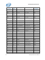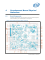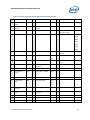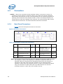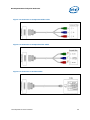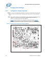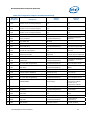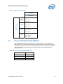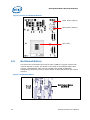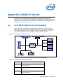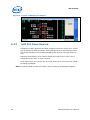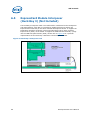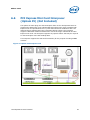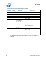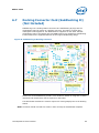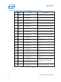
1
Intel® CoreTM 2 Duo Processor
and Intel® GM45 Express Chipset
(with DDR3 System Memory)
Development Kit User’s Manual
September 2008
Document Number: 320249-001
INFORMATION IN THIS DOCUMENT IS PROVIDED IN CONNECTION WITH INTEL® PRODUCTS. NO LICENSE, EXPRESS OR
IMPLIED, BY ESTOPPEL OR OTHERWISE, TO ANY INTELLECTUAL PROPERTY RIGHTS IS GRANTED BY THIS DOCUMENT. EXCEPT
AS PROVIDED IN INTEL'S TERMS AND CONDITIONS OF SALE FOR SUCH PRODUCTS, INTEL ASSUMES NO LIABILITY
WHATSOEVER, AND INTEL DISCLAIMS ANY EXPRESS OR IMPLIED WARRANTY, RELATING TO SALE AND/OR USE OF INTEL
PRODUCTS INCLUDING LIABILITY OR WARRANTIES RELATING TO FITNESS FOR A PARTICULAR PURPOSE, MERCHANTABILITY,
OR INFRINGEMENT OF ANY PATENT, COPYRIGHT OR OTHER INTELLECTUAL PROPERTY RIGHT. Intel products are not intended
for use in medical, life saving, life sustaining, critical control or safety systems, or in nuclear facility applications.
Intel may make changes to specifications and product descriptions at any time, without notice.
Intel Corporation may have patents or pending patent applications, trademarks, copyrights, or other intellectual property rights
that relate to the presented subject matter. The furnishing of documents and other materials and information does not provide
any license, express or implied, by estoppel or otherwise, to any such patents, trademarks, copyrights, or other intellectual
property rights.
Designers must not rely on the absence or characteristics of any features or instructions marked “reserved” or “undefined.” Intel
reserves these for future definition and shall have no responsibility whatsoever for conflicts or incompatibilities arising from
future changes to them.
Intel processor numbers are not a measure of performance. Processor numbers differentiate features within each processor
family, not across different processor families. See http://www.intel.com/products/processor_number for details.
The Intel® CoreTM 2 Duo processor and Intel® GM45 Express Chipset may contain design defects or errors known as errata which
may cause the product to deviate from published specifications. Current characterized errata are available on request.
Contact your local Intel sales office or your distributor to obtain the latest specifications and before placing your product order.
Copies of documents which have an order number and are referenced in this document, or other Intel literature may be obtained
by calling 1-800-548-4725 or by visiting Intel's website at http://www.intel.com.
BunnyPeople, Celeron, Celeron Inside, Centrino, Centrino logo, Core Inside, Dialogic, FlashFile, i960, InstantIP, Intel, Intel logo,
Intel386, Intel486, Intel740, IntelDX2, IntelDX4, IntelSX2, Intel Core, Intel Inside, Intel Inside logo, Intel. Leap ahead., Intel.
Leap ahead. logo, Intel NetBurst, Intel NetMerge, Intel NetStructure, Intel SingleDriver, Intel SpeedStep, Intel StrataFlash, Intel
Viiv, Intel vPro, Intel XScale, IPLink, Itanium, Itanium Inside, MCS, MMX, Oplus, OverDrive, PDCharm, Pentium, Pentium Inside,
skoool, Sound Mark, The Journey Inside, VTune, Xeon, and Xeon Inside are trademarks or registered trademarks of Intel
Corporation or its subsidiaries in the United States and other countries.
*Other names and brands may be claimed as the property of others.
Copyright © 2007-2008, Intel Corporation. All Rights Reserved.
2
Development Kit User’s Manual
Contents
1
Introduction .....................................................................................................8
1.1
1.2
1.3
1.4
1.5
2
Getting Started...............................................................................................17
2.1
2.2
2.3
2.4
2.5
2.6
2.7
2.8
3
Content Overview...................................................................................8
Text Conventions ...................................................................................9
Glossary of Terms and Acronyms ............................................................10
Development Kit Technical Support .........................................................14
1.4.1
Online Support........................................................................14
1.4.2
Additional Technical Support .....................................................14
Related Documents...............................................................................15
1.5.1
Ordering Hard Copies of Documents...........................................15
Overview ............................................................................................17
Development Kit Contents .....................................................................17
Additional Required Hardware (Not Included in the Development Kit)...........18
Additional Required Software (Not included in the Development Kit) ............ 19
Workspace Preparation..........................................................................19
System Setup and Power-Up..................................................................20
2.6.1
Using the AC to DC Power Supply (Mobile Power Mode) ................21
Power Down ........................................................................................22
System BIOS .......................................................................................22
2.8.1
Configuring the BIOS ...............................................................22
2.8.2
Programming BIOS Using a Bootable USB Device .........................23
Development Board Features ............................................................................25
3.1
3.2
3.3
3.4
3.5
3.6
Block Diagram .....................................................................................25
Mechanical Form Factor.........................................................................25
Development Board Key Features ...........................................................26
Software Key Features ..........................................................................29
3.4.1
AMI BIOS ...............................................................................29
Thermal Management ...........................................................................30
System Features and Operation..............................................................30
3.6.1
Processor Support ...................................................................30
3.6.2
Processor Voltage Regulators ....................................................30
3.6.3
Front-Side Bus (FSB) ...............................................................30
3.6.4
Processor Power Management ...................................................30
3.6.5
Processor Active Cooling...........................................................31
3.6.6
Manual Processor Voltage ID (VID) Support ................................31
3.6.7
Chipset ..................................................................................31
3.6.8
System Memory ......................................................................31
3.6.9
Video Display..........................................................................32
3.6.10 PCIe Slots ..............................................................................32
3.6.11 PCI Slots................................................................................33
3.6.12 On-Board LAN.........................................................................33
3.6.13 Serial Peripheral Interface (SPI) ................................................33
3.6.14 Soft Audio/Soft Modem ............................................................34
Development Kit User’s Manual
3
3.7
3.8
3.9
3.10
4
Development Board Physical Reference ..............................................................46
4.1
4.2
4.3
4.4
4.5
4.6
4.7
Appendix A
A.4
A.5
A.6
A.7
Port 80-83 Add-in Card (Included) ..........................................................58
PCI Expansion Card (Thimble Peak 2) (Included) ......................................59
HDMI and Display Port Video Interface Add-In Card (Eaglemont) (Included) .59
A.3.1
Rework to Change Eaglemont Card from HDMI to Display Port .......60
A.3.2
AUX Pull Down Rework.............................................................62
Intel® High Definition Audio Interposer Card (Mott Canyon 4) (Not Included)63
A.4.1
Mott Canyon 4 Jumper Settings .................................................64
ExpressCard Module Interposer (Duck Bay 3) (Not Included) ......................66
PCI Express Mini Card Interposer (Upham IV) (Not Included)......................67
Docking Connector Card (Saddlestring II) (Not Included) ...........................69
Rework Instructions ........................................................................................71
B.1
B.2
B.3
B.4
B.5
4
Board Components ...............................................................................46
Connectors ..........................................................................................48
4.2.1
Back Panel Connectors .............................................................48
Configuration Settings...........................................................................50
4.3.1
Configuration Jumpers/Switches ................................................50
4.3.2
BSEL Jumper Settings ..............................................................52
Power and Reset Push Buttons ...............................................................53
Net Detect Button ................................................................................54
LEDs ..................................................................................................55
Other Headers .....................................................................................56
4.7.1
H8 Programming Headers .........................................................56
4.7.2
Sideband and Test Headers.......................................................57
Add-In Cards..................................................................................................58
A.1
A.2
A.3
Appendix B
3.6.15 SATA Storage .........................................................................34
3.6.16 USB Connectors ......................................................................35
3.6.17 LPC Super I/O (SIO)/LPC Slot ...................................................36
3.6.18 Serial, IrDA ............................................................................36
3.6.19 Intel® 82802 Firmware Hub Device Support ...............................36
3.6.20 System Management Controller (SMC)/Keyboard Controller (KBC)..36
3.6.21 Clocks ...................................................................................37
3.6.22 Real Time Clock ......................................................................37
3.6.23 Thermal Monitoring .................................................................37
3.6.24 Power Supply Solution .............................................................38
3.6.25 Manual VID support for Graphics VR...........................................38
3.6.26 Debug Interfaces.....................................................................39
3.6.27 Board Form-Factor ..................................................................39
Power Management ..............................................................................39
3.7.1
Power Management States........................................................39
Testability ...........................................................................................40
Power Measurement Support..................................................................40
Power Supply Usage and Recommendation ..............................................45
Internal HDMI Enabling .........................................................................71
Enabling the Integrated Trusted Platform Module (iTPM) ............................71
Enabling External HDMI.........................................................................72
Support for Upham 4 ............................................................................72
Low Voltage High-Definition (HD) Audio Rework .......................................72
Development Kit User’s Manual
Appendix C
Programming System BIOS Using a Flash Programming Device .............................74
Appendix D
CPU Thermal Solution (Heatsink) Installation ......................................................75
Figures
Figure
Figure
Figure
Figure
Figure
Figure
Figure
Figure
Figure
Figure
Figure
Figure
Figure
Figure
Figure
Figure
Figure
Figure
Figure
Figure
Figure
Figure
Figure
Figure
Figure
Figure
Figure
Figure
Figure
Figure
Figure
1. Development Board Block Diagram.......................................................25
2. Silver Cascade Development Board Components ....................................46
3. Back Panel Connectors .......................................................................48
4. D-Connector to Component Video Cable ................................................49
5. D-Connector to Composite Video Cable .................................................49
6. D-Connector to S-Video Cable .............................................................49
7. Location of the Configuration Jumpers/Switches .....................................50
8. Power On and Reset Buttons ...............................................................54
9. Net Detect Button ..............................................................................54
10. Port 80-83 Interposer Card................................................................58
11. PCI Expansion Card (Thimble Peak 2) .................................................59
12. Eaglemont Add-in Card .....................................................................60
13. Location of Resistors for Rework (before Rework) .................................61
14. Location of Resistors for Rework (after Rework)....................................61
15. Location of Resistors for Rework.........................................................62
16. AUX Pull-Down Rework .....................................................................63
17. Mott Canyon 4 Interposer Card ..........................................................64
18. Duck Bay 3 Interposer Card...............................................................66
19. Upham IV Interposer Card.................................................................67
20. Saddlestring II Docking Connector......................................................69
21. iHDMI Rework Instruction 1 ...............................................................71
22. iHDMI Rework Instruction 2 ...............................................................71
23. Low Voltage HD Audio Rework (Always Rail) ........................................72
24. Low Voltage HD Audio Rework (Sus Rail).............................................73
25. Step 2 - Heatsink and Backplate.........................................................75
26. Step 4 - Backplate Pins .....................................................................76
27. Step 6 - Applying the Thermal Grease .................................................77
28. Step 7 - Squeezing Activation Arm .....................................................78
29. Step 8 - Installing the Heatsink ..........................................................79
30. Step 9 - Plugging in the Fan ..............................................................80
31. Step 10 - Completed Assembly ..........................................................81
Development Kit User’s Manual
5
Tables
Table
Table
Table
Table
Table
Table
Table
Table
Table
Table
Table
Table
Table
Table
Table
Table
Table
Table
Table
Table
Table
Table
Table
Table
Table
Table
6
1. Text Conventions ..................................................................................9
2. Definitions of Terms ............................................................................10
3. Acronyms ..........................................................................................11
4. Related Documents .............................................................................15
5. Intel Literature Centers........................................................................15
6. Development Board Feature Set Summary .............................................26
7. TV–Out Connections ............................................................................32
8. PCI Express Ports................................................................................33
9. Selection of I/O Voltage for the High Definition Audio...............................34
10. SATA Ports .......................................................................................34
11. USB Ports mapping............................................................................35
12. System Power Management States ......................................................39
13. System Power Management M-States...................................................40
14. Digital Multi-Meter Comparison ...........................................................41
15. System Voltage Rails .........................................................................41
16. Silver Cascade Development Board Components....................................47
17. Description of Back Panel Connectors ...................................................48
18. Configuration Jumpers and Switches Settings........................................51
19. BSEL Jumper Settings........................................................................53
20. Power-On and Reset Push buttons .......................................................53
21. LEDs ...............................................................................................55
22. H8 Programming Jumpers ..................................................................57
23. Jumper J1 Configurations ...................................................................58
24. Mott Canyon 4 Configuration Jumper/Switches Settings ..........................65
25. Upham IV Default Jumper/Switches Settings .........................................68
26. Board Rework to Support Display Port on Saddlestring ...........................70
Development Kit User’s Manual
Revision History
Document
Number
Revision
Number
320249
001
Description
Public launch release
Revision Date
September 2008
Note: The differences between the Pillar Rock (DDR2) and Silver Cascade (DDR3) User
Guides are in the DDR2 vs. DDR3 memory controller interface, the Configuration
Jumpers and Switches Settings Table and the Development Board Components Table.
All other components and references are the same between boards.
§
Development Kit User’s Manual
7
Introduction
1
Introduction
This user’s manual describes the use of the Intel® CoreTM 2 Duo Processor and Intel®
GM45 Express Chipset development kit with DDR3 SDRAM system memory. This
manual has been written for OEMs, system evaluators, and embedded system
developers. This document defines all jumpers, headers, LED functions, and their
locations on the development board, along with features of the board’s subsystems.
This manual assumes basic familiarity with installing and configuring hardware and
software in a personal computer system.
There are two development board options available as a part of this kit. The first
option uses DDR2 SDRAM memory. The DDR2 development board is referred to as
Pillar Rock. The second option uses DDR3 SDRAM memory. The DDR3 development
board is referred to as Silver Cascade. All other components and subsystems on the
boards are the same unless explicitly noted. This manual will cover the features and
details of the Silver Cascade development board.
For the latest information about the Intel® CoreTM 2 Duo processor and Intel® GM45
Express Chipset Development Kit, visit:
http://developer.intel.com/design/intarch/devkits/index.htm
For design documents related to the Intel® CoreTM 2 Duo processor and Intel® GM45
Express Chipset please visit:
Processor: http://developer.intel.com/design/intarch/core2duo/tech_docs.htm
Chipset:
1.1
http://www.intel.com/products/embedded/chipsets.htm
Content Overview
Chapter 1.0, “About This Manual” — This chapter contains a description of conventions
used in this manual. The last few sections explain how to obtain literature and contact
customer support.
Chapter 2.0, “Getting Started” — This chapter describes the contents of the
development kit. This chapter explains the basics steps necessary to get the board
running. This chapter also includes information on how to update the BIOS.
Chapter 3.0, “Development Board Features” — This chapter provides details on the
hardware features of the development board. It explains the Power Management and
Testability features.
Chapter 4.0, “Development Board Physical Reference” — This chapter provides a list of
major board components and connectors. It gives a descript ion of jumper settings
and functions. The chapter also explains the use of the programming headers.
Appendix A, “Add-In Cards” – This appendix contains information on add-in cards
available from Intel that can be used with the development board.
8
Development Kit User’s Manual
Introduction
Appendix B, “Rework Instructions” – This appendix contains rework instructions for
the development board and for some of the add-in cards to enable additional
supported features and functionality.
Appendix C, “Programming system BIOS using a flash programming device — This
appendix provides step by step instructions on programming the flash using a flash
programming device
Appendix D, “CPU Thermal Solution (Heatsink) Installation Instructions” — This
appendix gives detailed installation instructions for the Intel® CoreTM 2 Duo processor
heatsink.
1.2
Text Conventions
The notations listed in Table 1 may be used throughout this manual.
Table 1. Text Conventions
Notation
Definition
#
The pound symbol (#) appended to a signal name indicates that the signal
is active low. (e.g., PRSNT1#)
Variables
Variables are shown in italics. Variables must be replaced with correct
values.
Instructions
Instruction mnemonics are shown in uppercase. When you are
programming, instructions are not case-sensitive. You may use either
uppercase or lowercase.
Numbers
Units of Measure
A
GByte
KByte
KΩ
mA
MByte
MHz
ms
mW
ns
pF
W
V
µA
µF
µs
µW
Development Kit User’s Manual
Hexadecimal numbers are represented by a string of hexadecimal digits
followed by the character H. A zero prefix is added to numbers that begin
with A through F. (For example, FF is shown as 0FFH.) Decimal and binary
numbers are represented by their customary notations. (That is, 255 is a
decimal number and 1111 is a binary number. In some cases, the letter B
is added for clarity.)
The following abbreviations are used to represent units of measure:
amps, amperes
gigabytes
kilobytes
kilo-ohms
milliamps, milliamperes
megabytes
megahertz
milliseconds
milliwatts
nanoseconds
picofarads
watts
volts
microamps, microamperes
microfarads
microseconds
microwatts
9
Introduction
Notation
Signal Names
1.3
Definition
Signal names are shown in uppercase. When several signals share a
common name, an individual signal is represented by the signal name
followed by a number, while the group is represented by the signal name
followed by a variable (n). For example, the lower chip-select signals are
named CS0#, CS1#, CS2#, and so on; they are collectively called CSn#.
A pound symbol (#) appended to a signal name identifies an active-low
signal. Port pins are represented by the port abbreviation, a period, and
the pin number (e.g., P1.0).
Glossary of Terms and Acronyms
Table 2 defines terms used in this document.
Table 2. Definitions of Terms
10
Term/Acronym
Definition
Assisted Gunning
Transceiver Logic+
The front-side bus uses a bus technology called AGTL+, or Assisted
Gunning Transceiver Logic. AGTL+ buffers are open-drain, and require
pull-up resistors to provide the high logic level and termination. AGTL+
output buffers differ from GTL+ buffers with the addition of an active
pMOS pull-up transistor to assist the pull-up resistors during the first clock
of a low-to-high voltage transition.
Asynchronous
GTL+
The processor does not utilize CMOS voltage levels on any signals that
connect to the processor. As a result, legacy input signals such as A20M#,
IGNNE#, INIT#, LINT0/INTR, LINT1/NMI, PWRGOOD, SMI#, SLP#, and
STPCLK# utilize GTL+ input buffers. Legacy output signals (FERR# and
IERR#) and non-AGTL+ signals (THERMTRIP# and PROCHOT#) also
utilize GTL+ output buffers. All of these signals follow the same DC
requirements as AGTL+ signals, however the outputs are not actively
driven high (during a logical 0 to 1 transition) by the processor (the major
difference between GTL+ and AGTL+). These signals do not have setup or
hold time specifications in relation to BCLK[1:0], and are therefore
referred to as “Asynchronous GTL+ Signals”. However, all of the
Asynchronous GTL+ signals are required to be asserted for at least two
BCLKs in order for the processor to recognize them.
Infrared Data
Assoc.
The Infrared Data Association (IrDA) has outlined a specification for serial
communication between two devices via a bi-directional infrared data
port. The development board has such a port and it is located on the rear
of the board between the two USB connectors.
IMVP6+
The Intel Mobile Voltage Positioning specification for the Intel® Core™ 2
Duo Processor. It is a DC-DC converter module that supplies the required
voltage and current to a single processor.
Media Expansion
Card
The Media Expansion Card (MEC) provides digital display options through
the SDVO interface. The MEC card also incorporates video-in via a x1 PCI
Express* port.
Pad
The electrical contact point of a semiconductor die to the package
substrate. A pad is only observable in simulations.
Pillar Rock
The name of the development board in this development kit that uses
DDR2 SDRAM
Development Kit User’s Manual
Introduction
Term/Acronym
Definition
Pin
The contact point of a component package to the traces on a substrate,
such as the motherboard. Signal quality and timings may be measured at
the pin.
Silver Cascade
The name of the development board in this development kit that uses
DDR3 SDRAM
System Bus
The System Bus is the microprocessor bus of the processor.
System
Management Bus
A two-wire interface through which various system components may
communicate.
VCC (CPU core)
VCC (CPU core) is the core power for the processor. The system bus is
terminated to VCC (CPU core).
Table 3 defines the acronyms used throughout this document.
Table 3. Acronyms
Acronym
Definition
AC
Alternating Current
ACPI
Advanced Configuration and Power Interface
ADD2
Advanced Digital Display 2
ADD2N
Advanced Digital Display 2 Normal
AGTL or AGTL+
Assisted Gunning Transceiver Logic (See also Table 2 above)
AMI
American Megatrends Inc. (BIOS developer)
AMPS or iAMPS
(Intel) Adaptive Mobile Power System
AMT or iAMT
(Intel) Active Management Technology
ATA
Advanced Technology Attachment (disk drive interface)
ATX
Advance Technology Extended (motherboard form factor)
BGA
Ball Grid Array
BIOS
Basic Input/Output System
BSEL
Bus Select (Front Side Bus frequency control signals)
CL
Controller Link
CMOS
Complementary Metal-Oxide-Semiconductor
COM
Communications
CPU
Central Processing Unit (processor)
CRB
Customer Reference Board
DC
Direct Current
DC
Dual-Core
DDR
Double Data Rate
DDR2
Double Data Rate SDRAM version 2
DDR3
Double Data Rate SDRAM version 3
Development Kit User’s Manual
11
Introduction
Acronym
12
Definition
DIMM
Dual Inline Memory Module
DMI
Direct Memory Interface
DOS
Disk Operating System
DP
Display Port
DPST or iDPST
(Intel) Display Power Savings Technology
EBL
Extended Battery Life
EC
Embedded Controller
ECC
Error Correcting Code
EHCI
Enhanced Host Controller Interface
EMA
Extended Media Access
eSATA
External SATA (Serial ATA)
ESD
Electrostatic Discharge
FCBGA
Flip Chip Ball Grid Array
FCPGA
Flip Chip Pin Grid Array
FS
Full-speed. Refers to USB
FSB
Front Side Bus
FWH
Firmware Hub
GbE
Gigabit Ethernet
GLCI
Gigabit LAN Connect Interface
GM45
Intel® GM45 Express Graphics and Memory Controller Hub
GMCH
Graphics and Memory Controller Hub
GND
Ground (VSS)
GPIO
General Purpose Input/Output
HDA
High Definition Audio
HDMI
High Definition Media Interface
HS
High-speed. Refers to USB
ICH
I/O Controller Hub
ICH9M
I/O Controller Hub 9M (Mobile)
IDE
Integrated Drive Electronics
IMVP-6+
(or Intel MVP-6+)
Intel Mobile Voltage Positioning – revision 6+
I/O
Input / Output
IrDA
Infrared Data Association
ITP
Integrated Test Port
KBC
Keyboard Controller
Development Kit User’s Manual
Introduction
Acronym
Definition
L2
Level-2 (Cache)
LAN
Local Area Network
LED
Light Emitting Diode
LPC
Low Pin Count
LS
Low-speed. Refers to USB
LV
Low Voltage
LVDS
Low Voltage Differential Signaling (Video Standard)
mBGA
Mini Ball Grid Array
MEC
Media Expansion Card
MHz
Mega-Hertz
MT/s
Mega Transfers per second
NMI
Non-Maskable Interrupt
OEM
Original Equipment Manufacturer
PEG
PCI Express Graphics
PCI
Peripheral Connect Interface
PCIe
PCI Express*
PCM
Pulse Code Modulation
POST
Power On Self Test
PS/2
Personal System/2 (Keyboard and Mouse Connector)
PSI2
Power Status Indicator - 2
PWM
Pulse Width Modulation
RAID
Redundant Array of Inexpensive Disks
RCA
(Type of Audio and Video Connector)
RTC
Real Time Clock
SATA
Serial ATA
SDVO
Serial Digital Video Output
SIO
Super Input/Output
SKU (SKU Number)
Stock Keeping Unit (Stock Keeping Unit Number)
SMC
System Management Controller
SODIMM
(or SO-DIMM)
Small Outline Dual In-line Memory Module
SOIC-8 or SOIC-16
Small Outline Integrated Circuit (8 or 16 pin package)
SPI
Serial Peripheral Interface
SPWG
Standard Panels Working Group - http://www.spwg.org/
SRC
Source (Clock)
Development Kit User’s Manual
13
Introduction
Acronym
Definition
SUT
System Under Test
TME
Technical Marketing Engineer
TPM
Trusted Platform Module
TV or TVO
Television (Output)
µBGA
Micro Ball Grid Array
UHCI
Universal Host Controller Interface
ULV
Ultra-Low Voltage
USB
Universal Serial Bus
VGA
Video Graphics Adapter
VID
Voltage Identification
WiMAX
(Wireless Communications Standard)
WLAN
Wireless Local Area Network
VREG or VR
Voltage Regulator
WWAN
Wireless Wide Area Network
VCC
Power Signal
x1 (x2, etc)
By 1 (By 2, etc) (refers to number of PCIe Links)
XDP
eXtended Debug Port
1.4
Development Kit Technical Support
1.4.1
Online Support
Intel’s web site (http://www.intel.com/) provides up-to-date technical information and
product support. This information is available 24 hours per day, 7 days per week,
providing technical information whenever you need it.
1.4.2
Additional Technical Support
If you require additional technical support, please contact your Intel Representative or
local distributor.
14
Development Kit User’s Manual
Introduction
1.5
Related Documents
Table 4 lists publicly available documents related to this development kit. For
additional documentation, please contact your Intel Representative.
Table 4. Related Documents
Document Title
1.5.1
Location
Intel® Core™ 2 Duo Processor on 45-nm Process
Datasheet
http://www.intel.com/design/intarch
/core2duo/tech_docs.htm
Mobile Intel® 4 Series Express Chipset Family Datasheet
http://www.intel.com/design/chipset
s/embedded/gm45/techdocs.htm
Intel® I/O Controller Hub 9 (ICH9) Family Datasheet
http://www.intel.com/design/chipset
s/embedded/gm45/techdocs.htm
Montevina Platform Design Guide - For Intel® Core™ 2
Duo Mobile Processor Built on 45-nm Process
Technology, Mobile Intel® 45 Express Chipset and
82801IBM I/O Controller Hub (ICH9M)
Contact your Intel representative for
access to this document. (Doc
#355648)
Montevina Platform CRB Schematics – Silver Cascade
(DDR3) Customer Reference Board for Mobile Penryn
Processor, Cantiga and ICH9M Chipset
Contact your Intel representative for
access to this document. (Doc
#355669)
Ordering Hard Copies of Documents
To order hard copies of product literature, do the following:
1. Determine the SKU Number
The SKU number is listed at the bottom of the download page for that document.
It is also usually the first 6 digits of the name of the PDF file, such as:
12345612.pdf.
2. Call or E-mail a Request
Call: To place an order for a publication or text in hardcopy or CD form, please
contact the Intel Literature Fulfillment Centers listed in Table 5.
Table 5. Intel Literature Centers
Location
Telephone Number
U.S. and Canada
1-800-548-4725
International
1-303-675-2148
Fax
1-303-675-2120
Development Kit User’s Manual
15
Introduction
Email: To order a publication or text in hardcopy or CD form, send your request
to: [email protected]
Please make sure to include in your e-mailed request:
SKU #
Company name
Your name (first, last)
Full mailing address
Daytime phone number in case of questions
Note: Please be aware not all documents are available in all media types. Some may only be
available as a download.
§
16
Development Kit User’s Manual
Getting Started
2
Getting Started
This chapter identifies the development kit’s key components, features and
specifications. It also details basic development board setup and operation.
2.1
Overview
The development board consists of a baseboard populated with the Intel® CoreTM 2
Duo processor, the Intel® GM45 Express Chipset, other system board components and
peripheral connectors.
2.2
Development Kit Contents
The following hardware, software and documentation is included in the development
kit. Check for damage that may have occurred during shipment. Contact your sales
representative if any items are missing or damaged.
•
Letter to the Customer
•
Development Kit User’s Manual (this document)
•
Software CD-ROM, which includes (see the readme.txt file for a complete list of
CD-ROM contents):
⎯ Embedded system BIOS
⎯ BIOS installation utilities
⎯ Chipset drivers
⎯ Intel Embedded Graphics Drivers
⎯ Intel® Active Management Technology (AMT) software installation kit
•
Pre-assembled development system, which includes:
⎯ Silver Cascade development board
⎯ Plexiglass stand with Acrylic pad
⎯ Mounting screws and standoffs (installed)
⎯ Intel® CoreTM 2 Duo processor with 4 MB L2 Cache on 65nm process in the
478 pin Flip-Chip Pin Grid Array (Micro-FCPGA) package (Installed)
⎯ Processor thermal solution and CPU back plate
⎯ Intel® GM45 Express Chipset Graphics and Memory Controller Hub (GMCH)
⎯ GMCH (GM45) heatsink
⎯ I/O Controller Hub 9M (ICH9M)
⎯ Type 2032, 3 V lithium coin cell battery
⎯ One 512 MByte, 200 Pin, DDR3 SO-DIMM
⎯ Port 80 display card
⎯ Power Supply
⎯ 80 GByte SATA Hard Disk Drive
⎯ DVD-ROM Drive
⎯ Disk Drive Power and SATA Cables
•
One HDMI and Display Port add-in card (codename Eaglemont)
•
One PCI Extension Card (codename Thimble Peak 2)
•
One AC to DC Power Adapter
Document Number: 320249-001
Getting Started
2.3
Additional Required Hardware (Not Included in
the Development Kit)
The following additional hardware may be necessary to operate the development
board.
VGA Monitor: Any standard VGA or multi-resolution monitor may be used. The setup
instructions in this chapter assume the use of a standard VGA monitor or LCD
monitor.
Keyboard: The development board supports both PS/2 and USB style keyboards.
Mouse: The development board supports both PS/2 and USB style pointing devices.
Hard Drives and Optical Disc Drives and cables: One SATA hard disk drive and
one SATA optical DVD Drive are included in the development kit. Up to four SATA
drives and two IDE devices (master and slave) may be connected to the development
board. An optical disc drive (included) may be used to load the OS. All these storage
devices may be attached to the board simultaneously.
Video Adapter Card: Integrated video is output from the VGA connector on the back
panel of the development board. Alternately, a standard PCI Express* video adapter
card, ADD2 card or MEC video adapter card may be used for additional display
flexibility. Please contact the respective vendors for drivers and software for adapters
not provided with this development kit. Check the BIOS and the graphics driver,
where appropriate, for the proper video output settings.
Network Adapter and cables: A Gigabit network interface is provided on the
development board. The network interface will not be operational until after all the
necessary drivers are installed. A standard PCI/PCI Express* adapter may be used in
conjunction with, or in place of, the onboard network adapter. Please contact the
respective vendors for drivers and necessary software for adapters not provided with
this development kit.
You must supply appropriate network cables to utilize the LAN connector or any other
installed network cards.
Other Devices and Adapters: The development board functions much like a
standard desktop computer motherboard. Most PC-compatible peripherals can be
attached and configured to work with the development board.
18
Development Kit User’s Manual
Getting Started
2.4
Additional Required Software (Not Included in
the Development Kit)
The following additional software may be necessary to operate the development
board.
Operating System: The user must supply any needed operating system installation
files and licenses.
Application Software: The user must supply any needed application software.
2.5
Workspace Preparation
Caution: The development kit is shipped as an open system to provide flexibility in changing
hardware configurations and peripherals in a lab environment. Since the board is not in a
protective chassis, the user is required to take the following safety precautions in handling
and operating the board.
3.
The power supply cord is the main disconnect device to main power (AC power).
The socket outlet should be installed near the equipment and should be readily
accessible.
4.
To avoid shock, ensure that the power cord is connected to a properly wired and
grounded receptacle.
5.
Ensure that any equipment to which this product will be attached is also
connected to properly wired and grounded receptacles.
6.
Use a flame retardant work surface.
7.
Ensure a static-free work environment before removing any components from
their anti-static packaging. Wear an ESD wrist strap when handling the
development board or other development kit components. The development board
is susceptible to electrostatic discharge (ESD) damage, and such damage may
cause product failure or unpredictable operation.
Development Kit User’s Manual
19
Getting Started
2.6
System Setup and Power-Up
Complete the following steps to operate the reference board.
These steps should already be completed in the kit. Check these items to ensure
that nothing came loose during shipment.
•
Place one or more DDR3 SO-DIMMs in the memory sockets, populating J5N1
and/or J5P1. The memory sockets are on the bottom side of the development
board.
•
Place the Intel® Core™ 2 Duo processor T9400 in socket U2E1 and lock in place
(make sure to align the chip to the pin 1 marking).
•
Attach the heatsink for the processor U2E1.
•
Install the configuration jumpers as shown in Section 4.3.1 of this document.
(Replacing detached 1-x jumpers is not required for proper board operation.)
•
Attach hard drive data cable from development board SATA Connector J6J3 to the
drive with the supplied SATA data cable.
•
Attach hard drive power from the ATX power supply to the drive.
•
Attach optical drive data cable from development board SATA Connector J6J2 to
the drive with the supplied SATA data cable.
•
Attach optical drive power from the ATX power supply to the drive.
•
Connect the ATX power supply to the board at connector J4J1.
The following steps need to be completed by the user:
20
1.
Attach the included CPU heatsink fan to the top of the CPU heatsink using the four
screws provided. Plug the fan power in at the CPU Fan connector J2B3.
2.
Connect a PS/2 keyboard at connector J1A1 (bottom) or connect a USB keyboard
in one of the USB connectors.
3.
Connect a PS/2 mouse at connector J1A1 (top) or a connect a USB mouse in one
of the USB connectors.
4.
If using the chipset’s integrated graphics, connect a monitor to the VGA Video
output connector J2A2 with a VGA cable.
5.
If using an external graphics card, plug a PCIe graphics card in the PCIe x1 slot
J8B3 or a PCI Express Graphics card in the PCIE x16 slot J6B2. Connect a monitor
to the card.
6.
For mobile power configuration, unplug the ATX power supply from J4J1. Plug a
mobile Intel® AMPS AC to DC power adapter into J1G9. Optionally plug in a
battery pack into J1H1 or J1H2. Do not mix mobile and desktop power
configurations.
7.
Plug in the power cord of the ATX power supply or the Intel AMPS AC brick into a
standard 120 V or 240 V AC power outlet.
Development Kit User’s Manual
Getting Started
Powering up the board:
1.
Switch the power supply on (1) at the switch on the rear of the supply.
2.
Press the power button located at SW1C1.
3.
As the system boots, press F2 to enter the BIOS setup screen.
4.
Check time, date, and configuration settings. The default settings should be
sufficient for most users.
5.
Insert an operating system installation disk into the optical drive.
6.
Press F10 to save and exit the BIOS setup.
7.
The system reboots begins to install the operating system from the optical drive.
Note: An operating system disk is not included in this kit and operating system installation
will not be covered in this User Manual.
2.6.1
Using the AC to DC Power Supply (Mobile Power Mode)
There are a few limitations to development board operation when using the AC to DC
power adapter (mobile power mode).
First, do not mix mobile and desktop power configurations. Unplug the ATX power
supply from connector J4J1 before plugging in the AC to DC Power Adapter to
connector J1G9.
Second, desktop peripherals, including add-in cards, will not work when the board is
powered by the AC to DC power adapter or a battery (mobile power mode). If desktop
peripherals are used, the development board must be powered using the included ATX
power supply (desktop power mode).
Warning: Do not mix mobile and desktop power configurations. Unplug the ATX power supply
from connector J4J1 before plugging in the AC to DC Power Adapter to connector J1G9, or a
battery (not included) to connector J1H1-J1H2
Warning: The power supply cord is the main disconnect device from main AC power. The power
outlet shall be installed near the equipment and shall be readily accessible.
Development Kit User’s Manual
21
Getting Started
2.7
Power Down
Powering down the board:
There are three options for powering-down the system:
•
Power down from the operating system via the Windows Start Menu, or
equivalent.
•
Press the power button on the motherboard at SW1C1 to begin power-down.
•
If the system is hung, it is possible to asynchronously shut the system down by
holding down the power button (SW1C1) continuously for 4 seconds.
Note: We do not recommend powering down the board by shutting off power at the ATX
power supply.
Note: If the power button on the ATX power supply is used to shut down the system, wait at
least five seconds before turning the system on again to avoid damaging the system.
2.8
System BIOS
A version of the AMI* BIOS is pre-loaded on the development board.
Other BIOS vendors also support the Intel Core 2 Duo with Intel GM45 Express
Chipset. For additional BIOS support, please contact your BIOS vendor.
2.8.1
Configuring the BIOS
The default BIOS settings may need to be modified to enable or disable various
features of the development board. The BIOS settings are configured through a menudriven user interface which is accessible during the Power On Self Test (POST). Press
the F2 key or Delete key during POST to enter the BIOS interface. For AMI BIOS POST
codes, visit:
http://www.ami.com
For BIOS Updates please contact your Intel Sales Representative.
22
Development Kit User’s Manual
Getting Started
2.8.2
Programming BIOS Using a Bootable USB Device
The flash chips that store the BIOS and BIOS extensions on the development board
are connected to the SPI bus and are soldered down. One method of programming
these devices is through software utilities as described below. The software files and
utilities needed to program the BIOS are contained on the included CD-ROM. Another
method is described in Appendix C - Programming System BIOS Using a Flash
Programming Device.
Follow these steps to program the system BIOS using a bootable USB device:
1.
Prepare the workspace as outlined in Section 2.5 above.
2.
Setup the system as outlined in Section 2.6 above.
3.
Warning: Prior to flashing BIOS onto the platform AMT must be disabled in BIOS.
Failure to do this will render the system inoperable.
a) Switch on the power supply (to “1”).
b) Press the Power (PWR) Button on the development boar
c)
As the system starts to boot, enter the system BIOS setup by pressing
(F2) or (Del)
d) Navigate to AMT and select (disable)
e) Navigate to ”Save changes and exit”.
f)
Power off the system by pressing the power (PWR) button (SW1C1)
g) Turn off the power supply (remove power from the board) for at least
15 seconds
4.
Copy the following files and utilities to the Bootable USB Device:
•
BIOS Image Files
–
•
•
–
fpt.exe (DOS SPI Flash Utility)
–
fparts.txt (helper file)
MAC Address Programming Software Utility
–
•
spifull.bin
BIOS Programming Software Utilities
eeupdate.exe
Other helper files contained on the included CD-ROM
5.
Unplug the hard disk drive (HDD) SATA cable from the board at connector J6J3 so
that the board will boot from the bootable USB key.
6.
Record the 12 digit MAC Address of the board from the sticker near the CPU.
7.
Insert the bootable USB key into one of the USB ports on the development board.
8.
Switch on the power supply (to “1”).
9.
Press the Power (PWR) button on the development board.
10. Wait for the system to boot from the USB key to a DOS prompt.
11. From the DOS prompt (C:>), run the following and make sure that there are no
warnings or errors:
•
fpt –f spifull.bin
Development Kit User’s Manual
23
Getting Started
12. From DOS, run the following to reprogram the MAC address and make sure that
there are no warnings or errors:
•
eeupdate /nic=1 /mac=xxxxxxxxxxxx
(xxxxxxxxxxxx is the MAC Address from the sticker)
13. From DOS, run the following to update the keyboard and system controller flash
and make sure that there are no warnings or errors:
•
kscupdate ksc.bin
14. Power the system down by pressing the PWR button.
15. Clear the CMOS by performing the following:
h) Shunt the CMOS CLR jumper (J5H2 – near the on-board battery).
i)
Press the PWR button on the board. The board will not power on, but a couple
of LEDs will flash.
j)
Switch the power supply off to power down the board.
k) Remove the CMOS CLR jumper (J5H2).
16. Unplug the bootable USB key.
17. Verify correct BIOS installation:
a) Switch the power supply back on.
b) Press the PWR button on the board to power up the system.
c)
Boot to the BIOS Configuration screen by pressing F2 at the BIOS splash
screen.
d) In the BIOS main screen, check that the “Project Version” lists the correct
version of the BIOS.
e) Press the PWR key on the board to power the system back down.
18.
Re-connect the SATA data cable from the hard drive to the development
board at connector J6J3.
The system is now ready for normal operation.
§
24
Development Kit User’s Manual
Development Board Features
3
Development Board Features
3.1
Block Diagram
Figure 1. Development Board Block Diagram
CPU
GM45 GMCH
3.2
Mechanical Form Factor
The development board conforms to the ATX form factor. The development board will
fit in most standard ATX chassis. A list of add-in card connector and slot locations is
provided in Section 4.1 Internal and rear panel system I/O connectors are described in
Section 4.2.
Development Kit User’s Manual
25
Development Board Features
3.3
Development Board Key Features
Features of the development board are summarized in the following table.
Table 6. Development Board Feature Set Summary
Description
Comments
Processor
Intel® Core™ 2 Duo processor
T9400
479-pin Micro-FCPGA socket (Socket P) with
478-pin Micro-FCPGA package. 6MB L2 cache.
FSB 667/800/1067 MT/s support
Chipset
Intel® GM45 Express Graphics and
Memory Controller Hub (GM45
GMCH)
1299-pin Micro-FCBGA Package
ICH9M
Intel® ICH9M I/O Controller Hub
Two DDR3 SO-DIMM slots.
Maximum 8 GB using 2 Gb technology and
stacked SO-DIMMs.
Memory
Maximum 4 GB using 2 Gb technology and nonstacked SO-DIMMs.
Minimum capacity 256 MB using 512 Mb
technology
Supports DDR3 Frequency of 800 & 1067 MHz
Video
One PCI Express (PCIe) Graphics
Slot
One dual channel LVDS Connector
One VGA Connector
Support for SPWG3.5. 24 bit color panel support
(based on planned SPWG 4.0)
One TV D-Connector supporting SVideo, Composite video and
Component video
Support for two SDVO channels via x16 PCIe
connector (through add-in cards)
Spread spectrum clocking
PCI
PCI Express*
Intel GM45 Express Chipset supports four
monitors, but only has 2 video pipes which
support two screens each.
Support for UDI and native HDMI (via a x16
PCIe connector, usage through Eaglemont and
native HDMI through ADD card)
PCI revision 2.3 compliant (33MHz)
Three 5V PCI slots are supported
through PCI Extension card
No PCI slots on motherboard
Six x1 PCIe lanes
Revision 1.0a compliant
Five x1 connectors
Two sets of 2 in-line x1 PCIe slots
One x16 connector
Intel® 82567 GbE controller LAN on
motherboard (muxed with one PCIe lane)
Only one PCI gold finger on board
x2 PCIe lanes to docking via resistor stuffing
option
26
On-Board LAN
The Intel 82567 Gigabit Ethernet
LAN
The Intel 82567 is connected to ICH9M via LCI
interface and GLCI interface.
Wireless
Communication
Wireless LAN and Bluetooth support
via Upham 4 interposer
WLAN/WiMAX combo card Echo Peak support via
Upham 4
Development Kit User’s Manual
Development Board Features
Description
BIOS (SPI)
Comments
Supports two compatible flash
device
Support for multi-vendor SPI
BIOS (Intel®
82802 Firmware
Hub Device)
Support for 8-Mb Intel® 82802
Firmware Hub Device using Port 80
card
No Intel® 82802 Firmware Hub Device
connector on motherboard
Soft Audio/Soft
Modem
Intel® High Definition Audio (Intel®
HD Audio) MDC Header
Support visa interposer
Support multi package (SOIC-8 & SOIC-16)
device
Support only through port 80 add-in card
(through the TPM header)
Use Mott Canyon 4 daughter card (support via
sideband cable)
HDA routed to docking connector
ATA/Storage
4 SATA Ports
2 Cable Connector and 1 Direct Connect
Connector, one eSATA connector
Both port 0 & port 1 have interlock switch.
USB
12 USB 2.0/1.1 Ports
6 ports to Back-panel I/O connector, 5 ports to
Front-panel I/O connector and 1 port to Docking
LPC
One LPC slot
Includes sideband headers
SMC/KBC
Hitachi H8S/2117 micro-controller
ACPI compliant
Two PS/2 ports
One scan matrix keyboard connector
Clocks
CK-505D system clock and DB800M
Three 133/166/200/233/400 MHz CPU
differential clock pair
Twelve 100MhZ PCIe differential pair SRC clocks
Twelve 33 MHz PCI clocks
48-MHz USB clock, 14-MHz ref clock, 96-Mhz Dot
clock, Spread spectrum clocks
RTC
Battery-backed real time clock
Thermal
Monitoring
Processor temperature sensor
Processor
Voltage
Regulator
Intel MVP6+ for processor core
Power Supply
Desktop Mode
ATX Power Supply
Mobile Mode
Battery Pack (smart battery support)
Intel® Adaptive Mobile Power System (Intel®
AMPS) AC Brick
Development Kit User’s Manual
27
Development Board Features
Description
Debug
Interfaces
Comments
Port 80 display
Through Add-in card. Four seven-segment
displays
Extended Debug Port (XDP)
XDP connector (for processor run control)
Test points for manageability engine JTAG
LAI support
Intel® AMT
support
Intel® Active Management
Technology (Intel® AMT) is
supported on the CRBs with M0 M1,
and M-off management states
Intel® Turbo
Memory
Support
Intel® Turbo Memory technology of
hardware cache is supported using
an Intel Turbo Memory Add-in card
Power
Management
ACPI Compliant
Controller Link to GMCH and to wireless LAN
Manageability engine power plane
C0, C1, C1E, C2, C2E, C3, C3E, C4E, slow C4
exit, Intel® Enhanced Deeper Sleep (with Level
5 read) and Deep Power Down Technology
processor power states for mobility processors
S0 (Power On), S3 (Suspend to RAM), S4
(Suspend to Disk), S5 (Soft Off) system power
states.
M0 (All Wells powered), M1 (Main Well down,
Only ME power on), M-off (ME powered off)
manageability power states
Form Factor
ATX 2.2 like form factor
Miscellaneous
Extended Battery Life (EBL) support
10 layer board – 12” x 10.2”
Intel® Display Power Saving
Technology (Intel® DPST) 4.0
support
SPWG3.5 complaint LVDS panel
support
Mobile Digital Office initiatives
TPM1.2 and support for Trusted
Platform Enabling
Intel AMT support
Lead free design
Note: Review the document provided with the Development Kit titled “Important Safety and
Regulatory Information”. This document contains safety warnings and cautions that
must be observed when using this development kit.
28
Development Kit User’s Manual
Development Board Features
3.4
Software Key Features
The driver CD included in the kit contains all software drivers necessary for basic
system functionality under the following operating systems: Windows* XP/XP
Embedded, Windows Vista*, and Linux.
While every care was taken to ensure the latest versions of drivers were provided on
the enclosed CD at time of publication, newer revisions may be available. Updated
drivers for Intel components can be found at: http://downloadcenter.intel.com.
For all third-party components, please contact the appropriate vendor for updated
drivers.
Note: Software in the kit is provided free by the vendor and is only licensed for evaluation
purposes. Refer to the documentation in your evaluation kit for further details on any
terms and conditions that may be applicable to the granted licenses. Customers using
the tools that work with Microsoft* products must license those products. Any targets
created by those tools should also have appropriate licenses. Software included in the
kit is subject to change.
3.4.1
AMI BIOS
This development kit ships with AMI* BIOS pre-boot firmware from AMI*
pre-installed. AMI* BIOS provides an industry-standard BIOS on which to run most
standard operating systems, including Windows* XP/XP Embedded, Linux*, and
others.
The AMI* BIOS Application Kit (available through AMI*) includes complete source
code, a reference manual, and a Windows-based expert system, BIOStart*, to enable
easy and rapid configuration of customized firmware for your system.
The following features of AMI* BIOS are enabled in the development board:
•
DDR2 or DDR3 SDRAM detection, configuration, and initialization
•
Intel® GM45 Express Chipset configuration
•
POST codes displayed to port 80h
•
PCI/PCI Express* device enumeration and configuration
•
Integrated video configuration and initialization
•
Super I/O configuration
•
Active Management Technology
•
RAID 0/1 support
Development Kit User’s Manual
29
Development Board Features
3.5
Thermal Management
The objective of thermal management is to ensure that the temperature of each
component is maintained within specified functional limits. The functional temperature
limit is the range within which the electrical circuits can be expected to meet their
specified performance requirements. Operation outside the functional limit can
degrade system performance and cause reliability problems.
The development kit is shipped with a heatsink thermal solution for installation on the
processor. This thermal solution has been tested in an open-air environment at room
temperature and is sufficient for development purposes. The designer must ensure
that adequate thermal management is provided for if the system is used in other
environments or enclosures.
3.6
System Features and Operation
The following sections provide a detailed view of the system features and operation of
the development board.
3.6.1
Processor Support
The Silver Cascade board design supports the Intel® Core™ 2 Duo processor T9400
(U2E1) in a 478-pin Micro-FCPGA (Flip Chip Pin Grid Array) package.
3.6.2
Processor Voltage Regulators
The reference board implements an onboard Intel® Mobile Voltage Positioning
Intel® MVP -6 regulator for the processor core supply. The core VR solution supports
PSI2. The VR will support up to 56 amps. Slow C4 exit is supported to reduce
perceptible audio noise caused by periodically exiting the C4 state.
3.6.3
Front-Side Bus (FSB)
The Front Side Bus (FSB) on the development board supports data rates of 667 MT/s
(167MHz quad pumped, FSB-667), 800 MT/s (200MHz quad pumped, FSB-800) &
1067 MT/s (266 MHz quad pumped, FSB-1067). The FSB is AGTL+ and will be running
at 1.05V.
3.6.4
Processor Power Management
Intel® Core™ 2 Duo processor T9400 supports C0-C6 power states. This processor
also supports C2E and C4E. Additionally, the processor supports a new processor
state, Intel Deep Power Down Technology, that brings the CPU leakage power down to
the lowest possible. DPWR# protocol is also supported on the development board
through signal H_DPWR#.
30
Development Kit User’s Manual
Development Board Features
3.6.5
Processor Active Cooling
The system supports PWM based FAN speed control. Fan circuitry is controlled by the
signal CPU_PWM_FAN signal from the EC (PWM signal from the H8 is driven high to
3.3 V and low to 0 V at about 40 kHz carrier frequency).
A 3-pin header J2B3 is provided to support FAN Tacho output measurement for the
CPU.
3.6.6
Manual Processor Voltage ID (VID) Support
The development board supports manual VID operation for processor VR. A jumper
J2B2 is provided to incorporate “VID override” to allow the overriding of CPU VID
outputs to the CPU VCC Core VR. The intent of this “VID override’ circuit is for ease of
debug and testing.
3.6.7
Chipset
The Intel® GM45 Express Chipset (GM45 Chipset) is included on the development
board. The chipset consists of the GM45 Graphics and Memory Controller Hub (GM45
GMCH) and the ICH9M I/O Controller Hub.
The GM45 GMCH provides a processor interface at 667, 800 or 1067 MHz and two
DDR3 memory interfaces running at 800 or 1067 MT/s. It supports internal graphics
(integrated LVDS, 2 SDVO channels, VGA, TVO, Display port) as well as external
graphics (through ADD-in card on a X16 PCI Express Graphics slot). It also supports a
manageability engine (Manageability JTAG signals brought to test point/8-pin header)
and is connected to the ICH device via a DMI bus.
The ICH features twelve USB 2.0/1.1 compatible ports (six back panel, five front panel
USB ports and one port to docking), 4 Serial ATA channels (two cable connects, one
direct connect, one eSATA port) , an Intel® High Definition Audio (Intel® HD Audio)
digital link, PCI 2.3 compliant interface (no slots on board, slots provided on thimble
peak card), LPC bus, six general purpose PCI Express 1.1a compliant lanes in which
sixth PCI Express lane is used for Gigabit LAN interface. ICH9M also provides
Manageability support (controller link to GMCH and to wireless LAN).
3.6.8
System Memory
The development board supports a dual channel DRR3 interface. There are two DDR3
SO-DIMM sockets (J4P1 & J4N1) on the development board. The GMCH supports four
ranks of memory at 800 or 1067 MT/s on the board. The maximum amount of
memory supported on the Intel® GM45 Express Chipset is 8 GB of DDR3 memory by
utilizing 2 Gb technology in stacked SO-DIMMs and 4 GB of DDR3 memory by utilizing
2 Gb technology in non-stacked SO-DIMMs. Minimum capacity supported is 256 MB
using 512 Mb technology. There is no ECC support on this development board.
Development Kit User’s Manual
31
Development Board Features
3.6.9
Video Display
The reference board has six options for displaying video: VGA, LVDS, TVOUT, SDVO,
Display port (through Add in card) or PCI Express Graphics (PEG). Display port, SDVO
and PCI Express Graphics (PEG) are multiplexed on the same pins within the chipset.
The development board contains one DP/SDVO/PCI Express Graphics Slot (J6B2) for a
PCI Express compatible graphics card or an SDVO compatible graphics card (ADD2N &
ADD2R), one LVDS connector (J6F1), one TV-OUT D-connector (J2A1), and one 15-pin
VGA connector (J2A2). To support ADD2R (with PCI graphic lanes reversed), resistor
R1U4 should be made “NO STUFF”.
By default the voltage supplied to the SDVO/PCI Express Graphics slot is switched off
in suspend mode, and the reset signal is not gated. A stuffing option allows the
voltage to be supplied from voltage rails that stay on in suspend mode. A different
stuffing option allows the reset signal to be gated as well. Details of these stuffing
options can be referred on page 19 of the Silver Cascade schematics.
The TV is output through a D-connector. There are two cables in order to access TV: a
black D-connector to S-video (IPN: C87694-001) and a black D-connector to 3 pin
component (IPN: C87695-001). The blue coax pin can be used for composite TV
interface. To use a non-high definition external display with the board, change the
resolution to 480 lines interlaced (480i) in the Internal Graphics Device properties.
Table 7. TV–Out Connections
D-connector Cable
Composite Video
Component Video
S–Video
Blue
Cable
TV
Red
Red
Green
Green
Blue
Blue
D-connector to S-video
Note: Composite video and component video both use the same cable.
3.6.10
PCIe Slots
The ICH9M I/O Controller Hub (ICH9M) provides 6 PCIE ports (x1). Port 6 is
multiplexed with Gigabit LAN Controller Interface. The reference board has five x1
PCIe slots (J6B1, J6D1, J8B3, J8D1 & J7B1). Three of the five slots, Slot 1, Slot 3, and
Slot 5, are located at standard expansion slot locations. The fourth and fifth slots, Slot
2 and Slot 4, are located in-line with Slot 1 and Slot 3 respectively.
Support for x2 on lane 1 and lane 2 (Port 1 can be configured as a x1 port or a x2 port
shared with port 2) and on Lane 3 and lane 4 (port 3 can be configured as a x1 port or
a x2 port shared with port 4) can be configured via the ICH9M “RPC – Root Port
Configuration” register.
32
Development Kit User’s Manual
Development Board Features
Table 8. PCI Express Ports
ICH9M
PCIe Port
Default Destination
Optional Destination
1
PCIe Slot 1 (J6B1)
PCIe Docking (1st lane)
2
PCIe Slot 2 (J6D1) (in-line with Slot 1)
PCIe Docking (2nd lane)
3
PCIe Slot 3 (J8B3)
4
PCIe Slot 4 (J8D1) (in-line with Slot 3)
5
PCIe Slot 5 (J7B1)
6 (GLCI)
Intel 82567 LAN
C-link south routed to this slot. WLAN card
support through Upham3 Add-in card
Muxed with PCIe slot5 (only for testing)
Slot 4 also supports controller link. Upon a net detect event, Slot 4 gets a switched
Auxiliary 3.3 V supply.
3.6.11
PCI Slots
The reference board does not have any PCI slots on the motherboard. Three 5V PCI
slots are supported via the Thimble Peak PCI Extension Card.
3.6.11.1
PCI Gold-Fingers
A gold-finger connector (S9B1) is also supplied on the development board, which
allows an external PCI expansion board, Thimble Peak 2, to connect to it. Thimble
Peak 2 has three additional PCI slots allowing the user greater expansion. See
Appendix A for more information on the Thimble Peak 2 add-in card.
3.6.12
On-Board LAN
The development board provides 10/100/1000 LAN through EU8A1. Intel ® 82567 is
used on the reference board. The 82567 component is connected to the ICH9M chipset
through the LAN Connect Interface (LCI) and supports 10/100Mbps link. The same
device is connected through GLCI interface and supports 1000Mbps link. 82567
connect to an RJ45 connector at J5A1 with built in magnetic decoupling.
3.6.13
Serial Peripheral Interface (SPI)
The Serial Peripheral Interface on ICH9M can be used to support two compatible flash
devices (U8C1 (or U8B2), U8C4 (or U8C3)). Both the SPI devices supports for multipackage (SOIC-8 and SOIC-16) device. The SOIC-8 package (U8C1 & U8C4) would
support 16 Mb SPI flashes, while the SOIC-16 package (U8B2 & U8C3) will support
32Mb or higher SPI flash. Unified BIOS code (BIOS+ IAMT+ LAN) resides in these two
SPI devices.
Note: Out of the SOIC-8 and SOIC-16 footprints supported on the board only one of these
can be used at a time and on the board the Footprint is arranged one over the other.
By default, U8C1 (16Mb on CS#0) and U8C4 (16Mb on CS#1) will be stuffed.
Development Kit User’s Manual
33
Development Board Features
Note: SPI programming details are given in Section 2.8.2
3.6.14
Soft Audio/Soft Modem
Intel® High Definition Audio functionality is enabled through the Mott Canyon 4
Daughter Card. ICH9M supports 4 Intel® High Definition Audio codec. All the four are
routed to MDC header through resistor stuffing option. By default Codec 0 & 1 will be
connected to MDC Card. An on-board header is provided at J9E2 and J9E4 for this
purpose. No direct connection is provided for the Intel® High Definition Audio Card on
the development board; the Mott Canyon 4 card is required to enable the Intel® High
Definition Audio functionality. See Appendix A for more information on the Mott
Canyon 4 card.
The development board supports low voltage (LV) High definition codecs I/O. R8E7,
R8E8 & R7H2, R7H3 resistors are used to select between 3.3V I/O and 1.5VI/O.
Table 9. Selection of I/O Voltage for the High Definition Audio
3.6.15
I/O Voltage for the High
Definition Audio
STUFF
NO STUFF
3.3V (Default)
R8E7, R7H3
R8E8, R7H2
1.5V
R8E8, R7H2
R8E7, R7H3
SATA Storage
The development board provides four serial ATA (SATA) connectors. One of the four
serial ATA (SATA) connectors is a “direct connect” connector located at J8J1 (port 0
from ICH9M). The other two serial ATA connectors are “cable connect” connectors
located at J6J3 (port 1 from ICH9M) & J6J2 (port 4 from ICH9M). Also, the
development board supports an eSATA connector located at J7J1 (port 5 of ICH9M).
The eSATA connector is available on the front edge of the board.
Additionally SATA port 4 can be made available at docking connector by stuffing
(C7W2, C7W3, C7V13 and C7V14) and making C7H1, C7H2, C7G9 and C7G8 to “NO
STUFF”.
Table 10. SATA Ports
SATA Port
Connection Type
Connector
Port 0
Direct Connect
J8J1
Port 1 & Port 4
Cable Connect
J6J3 & J6J2
Port 5
eSATA
J7J1
These connectors mentioned in Table 10 are for the serial data signals. The board has
a power connector J5J1 to power the serial ATA hard disk drive. A green LED at
CR7H1 indicates activity on the ATA channel.
34
Development Kit User’s Manual
Development Board Features
The development board shares the power connector for both SATA ports. Due to this
only one of the serial ATA channel (Port1 by default) supports hot swapping capability.
Hot swap on Port 1 can be used only when the Port 4 is not used. Y-Power cable needs
to be connected first to the device on Port 1 before connecting the signal cable. When
hot swap is not desired, both Port 1 and Port 2 can be used. A jumper J7H1 is
provided to enable hot plug/removal on port-1. For jumper setting details refer to
Section 4.3.1, Table 18.
Note: The eSATA drives should be externally powered. Hence, there is no power supply
support for them on the motherboard
3.6.16
USB Connectors
ICH9M provides a total of twelve USB 2.0/1.1 ports. 6 USB ports (0, 2, 4, 6, 8, 10)
are connected to the back-panel I/O connector, 6 ports (1, 3, 5, 7, 9, 11) to the frontpanel I/O connector (of these ports, port 9 is also routed to Docking).
Four ports (0, 2, 4, and 6) are routed to a 4 stacked USB connector (J3A1) at the back
panel. The other 2 ports (8 and 10) are routed to the RJ45+Dual USB stacked
connector (J5A1) at the back panel.
Six USB ports are routed to USB 2X5 front panel headers: Port (1, 3) at J6H4, Port (5,
7) at J6H2 and Port (9, 11) at J6J1. The remaining one USB port is routed to docking
connector J9C2.
Note: The USB Port 9 is routed to the docking station interface by default. By changing the
straps near ICH9M Port 9 can be routed to the front panel header also. The advantage
of this scheme is that Port 9 can be tested on the motherboard without using the
docking card.
Table 11. USB Ports mapping
USB Port
Panel
Connector
Port 0, Port2, Port4,
Port 6
Back Panel I/O Connector
J3A1 (4 stacked USB Connector)
Port 1 & Port 3
Front Panel I/O Header
J6H4
Port 5 & Port 7
Front Panel I/O Header
J6H2
Port 8 & Port 10
Back Panel I/O Connector
J3A1 (RJ45 with Dual USB Connector)
Port 9 & Port 11
Front Panel I/O Header
(port 9 is routed to J6J1
through strapping option)
J6J1
Port 9
Docking Connector
(default)
J9C2
Development Kit User’s Manual
35
Development Board Features
3.6.17
LPC Super I/O (SIO)/LPC Slot
A SMSC SIO1007 serves as the SIO on the development board and is located at U7E3.
Shunting the jumper at J7E1 to the 2-3 positions can disable the SIO by holding it in
reset. This allows other SIO solutions to be tested in the LPC slot at J8E1. A sideband
header is provided at J9G1 for this purpose. This sideband header also has signals for
LPC power management. Information on this header is on sheet 49 of the Silver
Cascade schematics and is detailed in the “LPC Slot and Sideband Header
Specification”.
3.6.18
Serial, IrDA
The SMSC SIO chip incorporates a serial port, and IrDA (Infrared), as well as general
purpose IOs (GPIO). The Serial Port connector is provided at J2A2, and the IrDA
transceiver is located at U6A1. The IrDA transceiver supports SIR (slow IR), FIR (Fast
IR) and CIR (Consumer IR). The option to select between these is supported through
software and GPIO pin (IR_MODE) on the SIO.
3.6.19
Intel® 82802 Firmware Hub Device Support
It should be noted that the development board does not include an Intel 82802
Firmware Hub Device. Intel 82802 Firmware Hub Device support is provided through
the TPM header (J9A1). A Port 80 card with an Intel 82802 Firmware Hub Device
assembled can be used.
3.6.20
System Management Controller (SMC)/Keyboard
Controller (KBC)
A Renesas* H8S/2117 (U9G2) serves as both System Management Controller (SMC)
and Keyboard Controller (KBC) for the development board. The SMC/KBC controller
supports two PS/2 ports, battery monitoring and charging, wake/runtime SCI events,
CPU thermal monitoring/Fan control, GMCH thermal throttling support, LPC docking
support and power sequencing control.
The two PS/2 ports on the development board are for legacy keyboard and mouse.
The keyboard plugs into the bottom jack and the mouse plugs into the top jack at
J1A1. Scan matrix keyboards can be supported via an optional connector at J9E1.
36
Development Kit User’s Manual
Development Board Features
3.6.21
Clocks
The system clocks and spread spectrum clocks are provided by the CK505D (EU6H1)
clock synthesizer.
The FSB frequency is determined from decoding the processor BSEL settings. The
BSEL settings can be manually changed via jumpers J1G5, J1G3, and J1G1 (Refer to
Table 18).
The development board also supports PCIE CLKREQ through the DB800 SRC clock
buffer (U7C2). In addition this CRB also supports one dual 1x8 PCI fan-out buffer
(U7E4).
3.6.22
Real Time Clock
An on-board battery at BT5H1 maintains power to the real time clock (RTC) when in a
mechanical off state. A CR2032 battery is installed on the development board.
3.6.23
Thermal Monitoring
The processor has a thermal diode for temperature monitoring (the thermal sensor is
located at U3B3). The SMC throttles the processor if it becomes hot. If the
temperature of the processor rises too high, the SMC alternately blinks the CAPS lock
LED (located at CR9G2) and NUM lock LED (located at CR9G1) on the board, and the
board shuts down.
The development board supports PWM based FAN speed control. As part of the
thermal measurement, speed of the fan is varied based on the temperature
measurement. 3-pin fan headers J2B3 and J3C2 are provided to support FAN Tacho
output measurement for CPU and GMCH respectively.
Development Kit User’s Manual
37
Development Board Features
3.6.24
Power Supply Solution
The development board has the option to be powered from three different power
sources; an ATX power supply, an AC/DC switching power supply (‘Mobile Brick’), or
up to 2 external batteries. The board contains all of the voltage regulators necessary
to power the system up. There are two main supported power supply configurations,
Desktop and Mobile. The Desktop solution consists of only using the ATX power
supply. The Mobile solution consists of using the Mobile iAMPS AC Brick in conjunction
with the batteries. When the Mobile solution is being used either AC brick or batteries
can be plugged in. When both AC brick and the batteries are connected at the same
time, the batteries are monitored and charged if necessary.
Note: Desktop peripherals, including add-in cards, will not work in mobile power mode. If
desktop peripherals are used, the platform must be powered using desktop power
mode.
Note: Please use an “ATX12V” 1.1 Spec compliant power supply regardless of Vendor or
wattage level (an "ATX12V" rating means V5 min current =0.1 A, "ATX" V5 min
current = 1.0 A, among other differences). For example, the Sparkle Model No.
FSP300-60BTVS meets this requirement and is an ATX12V 1.1 Specification compliant
power supply.
Note: This development board uses the Intel AMPS solution for AC brick. For more details
refer to Intel® Adaptive Mobile Power System (Intel® AMPS) White Paper (Document
#603714) available from your Intel Representative
Note: If power button on the ATX power supply is used to shut down the system, please wait
at least 5 seconds before turning the system on again. We do not recommend
shutting down the system this way.
3.6.25
Manual VID support for Graphics VR
The development board supports manual VID operation for graphics Voltage
Regulator. Jumper J2H2 is provided to incorporate “VID override” to allow the
overriding of GMCH VID outputs to the graphics VR. The intent of this “VID override’
circuit is for ease of debug and testing. VID settings are contained in the IMVP6+
Specification (RS – Intel® IMVP-6 Mobile Processor and Mobile Chipset Voltage
Regulation Specification). Contact your Intel representative for access to this
document.
38
Development Kit User’s Manual
Development Board Features
3.6.26
Debug Interfaces
An XDP (Extended Debug Port) connector is provided at J1F1 for processor run control
debug support. This connector is compatible with both XDP and ITP-700. An external
adapter is used to interface ITPFlex700 cable to the platform. XDP incorporates new
run-control features on the JTAG interface and allows the user to communicate with
the processor or GMCH.
A port 80-83 display add-in card can also be used for debug. The port 80-83 add in
card could be used on the TPM header located at J9A1
Note: The XDP interface is backwards compatible with the ITP interface. However, an XDP to
ITP converter cable is necessary to use the older ITP tools. Also, in some cases a
resistor change rework is necessary to get the older ITP tools to function properly.
Please contact an Intel representative for additional details.
3.6.27
Board Form-Factor
The reference board form factor is similar to the full-size ATX specification and uses
10 layer board – 12” x 10.2”.
3.7
Power Management
3.7.1
Power Management States
Table 12 and Table 13 list the power management states that have been defined for
the development board. The system’s Controller Link (CL) operates at various power
level, called the M-states. M0 is the highest power state, followed by M1 and M-off.
Table 12. System Power Management States
State
Description
G0/S0/C0
Full on
G0/S0/C2
Quick Start: STPCLK# signal active
G0/S0/C3
Deep Sleep: CPUSTP# signal active
G0/S0/C4-C6
Deeper Sleep: Voltage to processor core is lowered (feature enabled by
software)
G1/S3
Suspend To RAM (all switched rails are turned off)
G1/S4
Suspend To Disk
G2/S5
Soft Off
G3
Mechanical Off
Development Kit User’s Manual
39
Development Board Features
Table 13. System Power Management M-States
M States
System
States
M0
S0
M1
M-off
Power Wells
DRAM
Intel ME Clocking
All wells powered
Powered
Clock chip powered and PLL,
DLL in use
S3-S5
Main well down
In self refresh; ME DRAM
controller on using
Channel A
Clock Chip powered with only
the GMCH clock running and
PLL, DLL in use
S3-S5
Main well down
Powered off (or self
refresh)
None, Intel ME powered off
The development board also supports CLKRUN#.
3.8
Testability
The development board provides an Extended Debug Port (XDP) for testing at J1F1
and direct processor probing. The XDP interface is backwards compatible with the
older ITP interface as well. The user must use an XDP or ITP interface that is
compatible with the Intel® Core™ 2 Duo processor T9400.
Note: The XDP interface is backwards compatible with the ITP interface. However, an XDP to
ITP converter cable is necessary to use the older ITP tools. Also, in some cases a
resistor change rework is necessary to get the older ITP tools to function properly.
Please contact your Intel representative for additional details.
3.9
Power Measurement Support
Power measurement resistors are provided on the platform to measure the power of
most subsystems. All power measurement resistors have a tolerance of 1%. The value
of these power measurement resistors are 2mΩ by default. Power on a particular
subsystem is calculated using the following formula:
P=
V2
R
R = value of the sense resistor (typically 0.002Ω)
V = the voltage difference measured across the sense resistor.
It is recommended that the user use a high precision digital multi-meter tool such as
the Agilent 34401A digital multi-meter. Refer to Table 14 for a comparison of a high
precision digital multi-meter (Agilent 34401A) versus a standard precision digital
multi-meter (Fluke 79).
2
40
Development Kit User’s Manual
Development Board Features
Table 14. Digital Multi-Meter Comparison
Example System
Sense Resistor Value:
0.002Ω
Voltage Difference Across Resistor:
1.492 mV (746 mA)
Calculated Power:
1.113 mW
Agilent 34401A (6 ½ digit display)
Fluke 79 (3 digit display)
Specification:
Specification:
±0.09% ±2 digits
(±0.0030% of reading)
+ (±0.0030% of range)
Min Voltage Displayed:
1.49193 mV
Min Voltage Displayed:
1.47 mV
Calculated Power:
1.1129 mW
Calculated Power:
1.08 mW
Max Voltage Displayed:
1.49206 mV
Max Voltage Displayed:
1.51 mV
Calculated Power:
1.1131 mW
Calculated Power:
1.14 mW
Error in Power:
±0.009%
Error in Power:
±0.3%
As Table 14 shows the precision achieved by using a high precision digital multi-meter
versus a standard digital multi-meter is ~33 times more accurate.
2
Table 15 summarizes all the power measurement sense resistors located on the
board. All sense resistors are 0.002Ω unless otherwise noted. Reference designators
marked with an asterisk are “not stuffed” on the board.
2
Table 15. System Voltage Rails
Component /
Interface
Voltage
Plane
Supply
Rail
Reference
Designator
CPU VR
5V
+V5S
+V5S_Intel® MVP6
R1B4
CPU VR
Battery
+VBAT
+VDC_PHASE
R1P6
CPU VR
1.05V
6262_PHASE1
+VCC_CORE
R3D1
CPU VR
1.05V
6262_PHASE2
+VCC_CORE
R2D1
CPU
1.05V
+V1.05S
+V1.05S_CPU
R3U2* & R3U1*
CPU
1.5V
+V1.5S
+VCCA_PROC
R3R14 (0.01Ω)
GMCH VR
Battery
+VBATA
1.05S_VIN
R4G3
GMCH VR
Battery
+VBATA
1.05M_VIN
R4V10
GMCH VR
Battery
+VBATA
1.5S_VIN
R5V5
GMCH VR
Battery
+VBAT
GVR_VBAT
R3V1
GMCH VR
5V
+V5S
+V5S_GVR
R3F4
GMCH VR
3.3V
+V3.3S_A_TV_DAC
R4F3
GMCH VR
1.05 V
Development Kit User’s Manual
+V3.3S_TVDAC
51124_LL2_L
+V1.05M
R4F7
41
Development Board Features
Component /
Interface
42
Voltage
Plane
Supply
GMCH VR
1.05 V
51124_LL1_L
GMCH VR
Battery
+VBATA
GMCH
1.05V
GMCH
Rail
Reference
Designator
+V1.05M
R4G4
1.05S_VIN
R4G3
+V1.05M
+VCC_GMCH
R5U3
VCCP
(1.05V)
+V1.05M
+VCCP_GMCH
R4F5
GMCH
1.05V
+V1.05M
+V1.05M_PEG_LR
R6E3
GMCH
1.05V
+V1.05M
+VCC_DMI
R5D7
GMCH
V_GFX
(1.05S)
+VCC_GFXCORE
+VGFX_CORE
R3F1
GMCH
1.05V
+V1.05M_CANTIGA
+V1.05M_A_SM_CK
R4R2
GMCH
1.05V
+V1.05M_CANTIGA
+V1.05M_PEGPLL
R5T8
GMCH
1.05V
+V1.05M_CANTIGA
+V1.05M_MCH_PLL
R5F12
GMCH
1.05V
+V1.05M_CANTIGA
V1.05M_MCH_PLL2
R4D6
GMCH
1.05V
+V1.05M_CANTIGA
+V1.05M_A_SM
R4R2
GMCH
1.5V
+V1.5S
+V1.5S_TVDAC
R4U3
GMCH
1.5V
+V1.5
+V1.5_DDR3_GMCH
R4D1
GMCH
1.8V
+V1.8S
+V1.8_DLVDS
R5F4
GMCH
3.3V
+V3.3S
+V3.3S_HV
R5F1
GMCH
1.5V
+V1.5S
+VCC_HDA
R5U1
GMCH
3.3V
+V3.3S_A_TV_CRT_BG
+V3.3S_A_DAC_BG
R5F5
GMCH
3.3V
+V3.3S_A_TV_CRT_BG
+V3.3S_A_TV_DAC
R4F3
PCIe Gfx
3.3V
+V3.3
+V3.3S_PEG
R6P2*
PCIe Gfx
3.3V
+V3.3S
+V3.3S_PEG
R6C1
PCIe Gfx
Battery
+VBATS_S4
+V12S_PEG
R6N6*
PCe Gfx
Battery
+VBATS
+V12S_PEG
R6N9
ICH
1.05V
+V1.05S
+V1.05S_ICH
R7F5
ICH
1.05V
+V1.05S
+V1.05S_ICH_IO
R6V10
ICH
1.5V
+V1.5S
+V1.5S_PCIE_R
R6G3
ICH
1.5V
+V1.5S
+V1.5S_SATA_ICH
R7G16
ICH
1.5V
+V1.5S
+V1.5S_USB_ICH
R7H1
ICH
3.3V
+V3.3S
+V3.3S_DMI_ICH
R6G6
ICH
3.3V
+V3.3S
+V3.3S_GLAN_ICH
R6U9
ICH
3.3V
+V3.3M_WOL
+V3.3M_ICH
R7U6
ICH
3.3V
+V3.3A
+V3.3A_ICH
R6F9
ICH
3.3V
+V3.3A
+V3.3A_USB_ICH
R7G1
Development Kit User’s Manual
Development Board Features
Component /
Interface
Voltage
Plane
Supply
Rail
Reference
Designator
ICH
3.3V
+V3.3S
+V3.3S_VCCPCORE_ICH
R7G14
ICH
3.3V
+V3.3M_WOL
+V3.3M_VCCPAUX
R7F2
ICH
3.3V
+V3.3S
+V3.3S_PCI_ICH
R7F4
ICH
3.3V
+V3.3S
+V3.3S_SATA_ICH
R7G9
Memory
Battery
+VBATA
1.5_VIN
R4A4
Memory
0.9 V
Memory
1.8V
+V1.5
+V1.5_DIMM0
R5C1
Memory
1.8V
+V1.5
+V1.5_DIMM1
R5B4
Memory
3.3V
+V3.3M
+V3.3M_DIMM0
R3C1 (0.022Ω)
Memory
3.3V
+V3.3M
+V3.3M_DIMM1
R4B13 (0.022Ω)
LAN
3.3V
+V3.3M_LAN_SW
+V3.3M_LAN
R7A2
LAN
1.8V
+V1.8_LAN
+V1.8_LAN_M
R8A11
LAN
1V
+V1.0_LAN_M
+V1.0_LAN_M_IN
R8A3
PCI
12V
+V12S
+V12S_PCI
R8B1
PCI
3.3V
+V3.3S
+V3.3S_PCI
R9D2
PCI
5V
+V5S
+V5S_PCI
R9B2
PCI
5V
+V5
+V5_PCI
R8B3
PCIe
12V
+V12S
+V12S_PCIESLOT1
R7N6
PCIe
12V
+V12S
+V12S_PCIESLOT2
R7C20
PCe
12V
+V12S
+V12S_PCIESLOT3
R8B2
PCIe
12V
+V12S
+V12S_PCIESLOT4
R8C4
PCIe
12V
+V12S
+V12S_PCIESLOT5
R7N2
PCIe
3.3V
+V3.3S
+V3.3S_PCIESLOT1
R7N5
PCIe
3.3V
+V3.3S
+V3.3S_PCIESLOT2
R7R1
PCIe
3.3V
+V3.3S
+V3.3S_PCIESLOT3
R7C1
PCIe
3.3V
+V3.3S
+V3.3S_PCIESLOT4
R8D2
PCIe
3.3V
+V3.3S
+V3.3S_PCIESLOT5
R7N4
Audio
1.5 V
+V1.5A_HDA_IO
+V3.3S_1.5S_HDA_IO
R8E8*
Audio
3.3 V
+V3.3A
+V3.3A_1.5A_HDA_IO
R8E7
Panel Bklt
5V
+V5S
+V5S_LVDS_BKLT
R6U20
Panel Bklt
Battery
+VBAT
+VCC_LVDS_BKLT
R6F15
Panel LVDS
3.3V
+V3.3S/+V5S
VDD_VDL
R6V2
Panel LVDS
3.3V
+V3.3S
+V3.3S_LVDS_DDC
R6U19*
Development Kit User’s Manual
+V0.9
+V0.75_R
R4B11
43
Development Board Features
Component /
Interface
44
Voltage
Plane
Supply
Rail
Reference
Designator
CK505
3.3V
+V3.3M
VDD_CK505
R5V12
CK505
3.3V
+V3.3S
+V3.3S_DB800
R7C9
CK505
1.05V
+V1.05M
+VDDIO_CLK
R5V8
LPC
3.3V
+V3.3
+V3.3_LPCSLOT
R8F1
LPC
5V
+V5
+V5_LPCSLOT
R8E3
TPM
5V
+V5
+V5_R1_TPM
R9M1
TPM
3.3V
+V3.3S
+V3.3S_R1_TPM
R9M2
TPM
3.3V
+V3.3A
+V3.3A_R1_TPM
R9A5
SMC
3.3V
+V3.3A
+V3.3A_KBC
R8H8
PS2
5V
+V5
+V5_PS2
R1A1
SIO
3.3V
+V3.3S
+V3.3S_SIO
R7T2
IR
3.3V
+V3.3S
+V3.3S_IR
R4M3
USB
5V
+V5A
+V5A_USBPWR_IN4
R7H15
USB
5V
+V5A
+V5A_USBPWR_IN3
R3B3
USB
5V
+V5A
+V5A_USBPWR_IN2
R7H5
USB
5V
+V5A
+V5A_USBPWR_IN1
R5W15
SPI
3.3V
+V3.3M_WOL
+V3.3M_SPI
R8R1
SATA
3.3V
+V3.3S
+V3.3S_SATAP0
R8Y1
SATA
5V
+V5S
+V5S_SATAP0
R8H12
SATA
12V
+V12S
+V12S_SATAP0
R8W14
SATA
3.3V
+V3.3S
+V3.3S_SATAP1
R6J3
SATA
5V
+V5S
+V5S_SATAP1
R4Y4
SATA
12V
+V12S
+V12S_SATAP1
R4Y3
System
Battery
+VCHGR_OUT
+VBS
R1G13 (0.02Ω)
System
Battery
AMPS_AD+_Q1
+VBS
R1H1 (0.007Ω)
System
Battery
+VBATA
51120_DRVH1_+VBATA
R3H18
System
Battery
+VBATA
51120_DRVH2_+VBATA_Q
R3H3
System
3.3V
51120VBST2_LR
+V3.3A_MBL
R3G5
System
5V
51120_+V5A_MBL_QL
+V5A_MBL
R3J2
System
ATX
+V5A
+V5_ATX
R4J1*
System
ATX
+V3.3A
+V3.3_ATX
R4W20*
System
ATX
+V12_ATX
+VBATA
R4Y2
System
ATX
-V12_ATX
-V12A
R4Y1
System
ATX
+V5SB_ATX
+V5SB_ATXA
R5H8
Development Kit User’s Manual
Development Board Features
3.10
Power Supply Usage and Recommendation
Do not use non-Sparkle ATX power supplies. Only use Sparkle ATX Desktop Power
Supplies.
As the Desktop ATX supplies grew to meet the increased power for those
Motherboards, their minimum loading requirements also grew. When you try to run a
mobile platform on it, it may not load the 5.0V rail enough to meet the minimum
loading requirements for it to maintain regulation.
Recommended power 20-pin ATX power supplies include:
•
Sparkle Model No. FSP300-60BTVS meets this requirement and is an ATX12V 1.1
Spec (note that this part may be End Of Life)
These 20-pin ATX power supplies may also work if you can't find the above model
number (lower power supplies are probably better):
•
Sparkle (SPI) FSP250-60BT, FSB300-60BT, FSB300-60BTV, FSP350, FSP40060GN (these supplies work in the lab, although are not checked against spec)
DO NOT use Delta or PowerMan ATX Supplies. You may experience the following
symptoms when using a non-Sparkle supply:
•
"post 00"
•
Blue Screen reporting driver or device issue when using a desktop PCI graphics
card
•
Hanging during boot with PEG or PCI graphics
•
PCI video only during boot, but not available after in Windows*.
§
Development Kit User’s Manual
45
4
Development Board Physical
Reference
4.1
Board Components
The following figure shows the major components of the Silver Cascade development
board, and Table 16 gives a brief description of each component.
Figure 2. Silver Cascade Development Board Components
Document Number: 320249-001
Development Board Physical Reference
Table 16. Silver Cascade Development Board Components
1
Chipset VR
EU5G1
19
SPI flash 1
U8C4
37
Battery B Connector
J1H2
2
Trusted Platform
Module
J9A1
20
SMC/KBC
J1A1
38
Battery A Connector
J1H1
3
82567 LAN
controller
EU8A1
21
Manufacturing Mode
Jumper
J9J1
39
iAMPS connector
EU2G1
4
PCI Express Slot 1
J6B1
22
Virtual Battery Switch
SW9H3
40
Intel® Core™ 2 Duo
processor T9400
U5E1
5
PCI Express Slot 2
J6D1
23
SATA Direct Connect
J8J1
41
VID LEDs
CR1B1
CR1B2
CR1B3
CR1B4
CR1B5
CR1B6
CR1B7
6
DB800 Clock Buffer U7C2
24
Front Panel Header
J6H5
42
Manual VID Override
Jumper
J2B2
7
PCI Gold-Fingers
25
SATA Cable Connect
J6J3
43
Teenah/Cantiga
U5E1
S9B1
J6J2
8
PCI Express Slot3
J8B3
26
SPI Flash 2
U8C1
44
PCI Express Graphics
Slot
J6B2
9
PCI Express Slot4
J8D1
27
SATA Port1,4 Power
Connector
J5J1
45
DDR3 VR
EU4N1
10
PCI Express Slot5
J7B1
28
Debug XDP – CPU
J1F1
11
Mott Canyon 4
Header
J9E2
29
Debug XDP – ICH9M
J8H2
12
SMSC SIO
U7E3
30
LVDS Connector
J6F1
13
Keyboard Scan
Matrix
J9E1
31
Front Panel USB
J6H4
J6H2
J6J1
14
LPC Docking
Connector
J9E3
32
CK-505 Derivative
EU6H1
15
LPC Sideband
Header
J9G1
33
ATX Power Supply
Connector
J4J1
16
LPC Slot
J8E1
34
RTC Battery
BT5H1
17
eSATA connector
J7J1
35
Docking connector
J9C2
18
ICH9M
U7F1
36
Graphics VR
EU3G1
Development Kit User’s Manual
47
Development Board Physical Reference
4.2
Connectors
Caution: Many of the connectors provide operating voltage (+5V DC and +12V DC, for
example) to devices inside the computer chassis, such as fans and internal peripherals.
Most of these connectors are not over-current protected. Do not use these connectors for
powering devices external to the computer chassis. A fault in the load presented by the
external devices could cause damage to the computer, the interconnecting cable, and the
external devices themselves. This section describes the board’s connectors.
4.2.1
Back Panel Connectors
Figure 3 shows the back panel connectors on the board.
Figure 3. Back Panel Connectors
Table 17. Description of Back Panel Connectors
Item
Description
Ref
Des
Item
J5A1
1
RJ-45 LAN + 2 USB Ports
2
IrDA Transceiver
3
Thermal Diode (no stuff)
4
4 USB Ports
U4A1
J4A1
Description
Ref Des
5
VGA (Bottom Side
Connector) + Serial Port
(Top Side Connector)
J2A2
6
D-connector
J2A1
7
PS/2 (Keyboard bottom –
Mouse Top)
J1A1
J3A1
Note: The on-board 14 pin D-Connector J2A1 (#6) supplies the necessary signals to support
the Composite, S-Video, and Component TV standards. Component video and
composite video are connected to the development board using a D-connector to
component video cable (with three RCA receptacles at one end and D-mating
connector on other end) (not included in the kit). S-video is connected to the board
using a D-connector to S-Video cable (with 4-pin DIN connector one end and
D-mating connector on other end) (not included in the kit).
48
Development Kit User’s Manual
Development Board Physical Reference
Figure 4. D-Connector to Component Video Cable
Figure 5. D-Connector to Composite Video Cable
Figure 6. D-Connector to S-Video Cable
Development Kit User’s Manual
49
Development Board Physical Reference
4.3
Configuration Settings
4.3.1
Configuration Jumpers/Switches
Caution: Do not move jumpers with the power on. Always turn off the power and unplug the
power cord from the computer before changing jumper settings. Else, it may damage the
board.
Note: Some jumpers may fall off during shipment. Jumpers that are only attached to one pin
(noted as 1-x) are more prone to becoming detached. Replacing detached 1-x
jumpers is not required for proper board operation.
Figure 7 shows the location of the configuration jumpers and switches. Table 18
summarizes the jumpers and switches and gives their default and optional settings.
The board is shipped with the jumpers and switches shunted in the default locations.
2
Figure 7. Location of the Configuration Jumpers/Switches
50
Development Kit User’s Manual
Development Board Physical Reference
Table 18. Configuration Jumpers and Switches Settings
#
Reference
Designator
Default
Setting
Description
Optional
Setting
1
J1G1
BSEL2 (Refer to BSEL Jumper Settings
Section 4.3.2 for Setting Changes)
1-2
1-X
2
J1G3
BSEL1 (Refer to BSEL Jumper Settings
Section 4.3.2 for Setting Changes)
1-2
1-X
3
J1G5
BSEL0 (Refer to BSEL Jumper Settings
Section 4.3.2 for Setting Changes)
1-2
1-X
4
J2B2
CPU CORE VID
All OPEN (CPU
5
J2G1
Force Shutdown
1-X (Normal Operation)
6
J2H2
GFX CORE VID
All OPEN
7
J3C1
CPU thermal sensor
1-2, 3-4
8
J3J2
Power ON Latch
1-X (Normal Operation)
1-2 Latch the power ON
9
J4H1
No ME G3 to M1 support
1-X
1-2 Jump power state from
G3 to M1
10
J4J2
SATA Power Enable
1-2 (Hot plug/removal
supported)
1-X Hot plug not supported
11
J5G1
SRTC RST
1-X (Keep ME RTC registers)
1-2 Clear ME RTC registers
12
J5H2
CMOS Clear
1-X (Normal Operation)
1-2 Clear the contents of
the CMOS
13
J7A1
In-circuit SMC Programming
1-2 (Normal Operation)
2-3 To Program the H8
14
J7E1
SIO Reset
1-2 (Normal Operation)
2-3 To hold the SIO in
RESET
15
J7H1
SATA interlock switch for port0
1-2 (Present)
1-X Removed
16
J7H2
TPM PHYSICAL PRESENCE
1-X (Not Present)
1-2 (Present)
17
J8B1
PM Lan enable
1-2 (LAN Enable)
2-3 LAN Disable
18
J8B2
In-circuit SMC Programming
1-2 (Normal Operation)
2-3 To Program the H8
19
J8C1
SELCETING SPI0 or SPI1 TO BE
PROGRAMMED
1-X (No device selected for
Programming)
1-2 SPI-0 to be
Programmed enabled
2-3 SPI-1 to be
Programmed enabled
20
J8F2
BIOS recovery
1-X (Normal Operation)
1-2 for BIOS recovery
21
J8G1
SV Setup
1-X (Normal Operation)
1-2 SV Setup
22
J8G3
SMC MD2
1-X
1-2 Advanced Single chip
mode
23
J8G4
CRB/SV Detect
1-X (CRB)
1-2 SV
24
J8G5
SMC MD1
1-2 (Normal Operation)
1-X No external
Programming
25
J8G6
KBC disable
1-X (KBC enabled
1-2 KBC disabled
Development Kit User’s Manual
1-2 Force the board to
shutdown
51
Development Board Physical Reference
#
Reference
Designator
Default
Setting
Description
Optional
Setting
26
J8H1
Boot BIOS Strap
1-2
1-X PCI to LPC
27
J9C1
PROGRAMMING SPI1
1-X
1-2 Program SPI-0
28
J9D1
PROGRAMMING SPI0
1-X
1-2 Program SPI-1
29
J9F1
KSC Enable
1-2
1-X
30
J9G2
Boot Block Programming
1-2 (Normal Operation)
1-X to Program the H8
31
J9H1
NMI
1-X
1-2 Disabled
32
J9H2
SATA interlock switch for port1
1-2 (Present)
1-X Disabled
33
J9H3
LID Position
1-X
1-2
34
J9H4
Virtual Battery
1-X
1-2
Note: A jumper consists of two or more pins mounted on the motherboard. When a jumper
cap is placed over two pins, it is designated as 1-2. When there are more than two
pins on the jumper, the pins to be shorted are indicated as 1-2 (to short pin 1 to pin
2), or 2-3 (to short pin 2 to pin 3). When no jumper cap is to be placed on the
jumper, it is designated as 1-X.
4.3.2
BSEL Jumper Settings
The jumper settings in Table 19 are provided to accommodate frequency selection for
the processor Power On and Reset Push Buttons.
52
Development Kit User’s Manual
Development Board Physical Reference
Table 19. BSEL Jumper Settings
Processor
Intel® Core™ 2 Duo
Processor
J1G5 Æ 1-2
CPU
Driven
J1G3 Æ 1-2
J1G1 Æ 1-2
J1G5 Æ Open
1067
FSB
J1G3 Æ 2-3
J1G1 Æ 2-3
Speed
J1G5 Æ open
(MHz)
800
J1G3 Æ open
J1G1 Æ 2-3
J1G5 Æ 2-3
667
J1G3 Æ Open
J1G1 Æ 2-3
4.4
Power and Reset Push Buttons
The development board has two pushbuttons: Power and Reset. The Power button
releases power to the entire board causing the board to boot. The Reset button forces
all systems to warm reset. The two buttons are located near the CPU close to the East
edge of the board. The Power button is located at SW1C1 and the Reset button is
located at SW1C2.
Table 20. Power-On and Reset Push buttons
Description
Component
Power Button
SW1C1
Reset Button
SW1C2
CPU
U2E1
Development Kit User’s Manual
53
Development Board Physical Reference
Figure 8. Power On and Reset Buttons
Power Button (SW1C1)
Reset Button (SW1C2)
CPU (U2E1)
4.5
Net Detect Button
The board has one Net Detect push button switch (SW8E1) to support wireless LAN
network detection in S0-S5. This button is connected on the SMC/KBC GPIO. When
pressed, a manageability wake event is signaled to the ICH9M via SMC/KBC,
manageability planes are powered, and the 82567 wireless LAN performs the network
detection.
Figure 9. Net Detect Button
54
Development Kit User’s Manual
Development Board Physical Reference
4.6
LEDs
The following LEDs provide status of various functions on the development board.
Table 21. LEDs
Function
Reference Designator
Keyboard number lock
CR9G1
Keyboard scroll lock
CR9G3
Keyboard caps lock
CR9G2
System State S0
CR5H4
System State S3
CR5H6
System State S4
CR5H7
System State S5
CR5H5
System State M0/M1
CR5H3
SATA Activity
CR7H1
VID Setting 0
CR1B1
VID Setting 1
CR1B2
VID Setting 2
CR1B3
VID Setting 3
CR1B4
VID Setting 4
CR1B5
VID Setting 5
CR1B6
VID Setting 6
CR1B7
System Power Good
CR7H3
LT Status
CR8G1
Development Kit User’s Manual
55
Development Board Physical Reference
4.7
Other Headers
4.7.1
H8 Programming Headers
The microcontroller firmware for system management/keyboard/mouse control can be
upgraded in two ways. The user can either use a special DOS* utility (in-circuit) or
use an external computer connected (remote) to the system via the serial port on the
board.
If the user chooses to use an external computer connected to the system via the serial
port, there are four jumpers that must be set correctly first. Please refer to Table 22
for a summary of these jumpers and refer to Figure 7 for the location of each jumper.
2
Required Hardware: One Null Modem Cable and a Host Unit with a serial COM port
(System used to flash the SUT).
Here is the sequence of events necessary to program the H8.
1.
Extract all files (keep them in the same folder) to a single directory of your choice
on the host machine or on a floppy disk.
2.
Connect a NULL modem cable to the serial ports of each platform (host and unit to
be flashed).
3.
With the board powered off, move the following jumpers to the programming
stuffing option.
4.
J9G2 (remove) (default: 1-2), Sets SMC_INIT_CLK high.
5.
J7A1 (2-3) (default: 1-2), link the Host Unit to On Board H8.
6.
J8B2 (2-3) (default: 1-2), link the Host Unit to On Board H8.
7.
J9H1 (1-2) (default: 1-X), disable 1 Hz Clock.
8.
Attach an AC brick or an ATX power supply to the system and power up the board.
9.
From the directory where you extracted the files, run the “kscflash ksc.bin /
remote” command to program the H8 via the serial port.
10. Follow the instructions the flash utility provides.
11. With the board powered off, return the jumpers to their default setting.
Note: Make sure the board is not powered on, and the power supply is disconnected before
moving any of the jumpers.
56
Development Kit User’s Manual
Development Board Physical Reference
Table 22. H8 Programming Jumpers
#
4.7.2
Jumper
1
Remote H8
Programming
2
Boot Block
Programming
3
1Hz clock
Reference
Designator
J7A1
Default Stuffing
Option
Programming Stuffing
Option
1-2 – normal
operation
2-3 – link the Host Unit to On
Board H8
J9G2
1-2 (IN) – normal
operation
OUT – set SMC_INIT_CLK high
(to program H8)
J9H1
OUT – normal
operation, clock
enabled
IN – clock disabled, enable H8
programming
J8B2
Sideband and Test Headers
Additional sideband and test headers are located on sheet 46 of the Silver Cascade
schematics.
§
Development Kit User’s Manual
57
Appendix A Add-In Cards
Of the add-in cards described in this appendix, only the Port 80-83 Card, PCI
Expansion Card (Thimble Peak 2) and the HDMI and Display Port Video Interface Card
(Eaglemont) are included in the development kit. Contact your Intel Representative to
obtain cards not included in the kit.
A.1
Port 80-83 Add-in Card (Included)
Port 80-83 Add-in card plugs to the CRB through TPM header. It also provides an
additional 10 pin LPC header for LPC supported interfaces. Port 80-83 card decodes
the LPC bus BIOS POST codes and displays on four 7-segment display. It also has
optional Intel® 82802 Firmware Hub Device footprint for BIOS support.
Figure 10. Port 80-83 Interposer Card
Jumper J1 is used for the configurations shown in the following table:
Table 23. Port 80-83 Display Configurations
Jumper J1
Open (None)
Description
AIC Intel® 82802 Firmware Hub Device Disabled
Display Ports 81-80
1-2
AIC Intel® 82802 Firmware Hub Device enabled
Display Ports 81-80
2-3
AIC Intel® 82802 Firmware Hub Device Disabled
Display Ports 83-82
Document Number: 320249-001
Add-In Cards
A.2
PCI Expansion Card (Thimble Peak 2)
(Included)
The PCI Expansion Card (Thimble Peak 2) is provided to offer 3 PCI slots and one
goldfinger PCI slot on the evaluation board. The expansion card also contains a floppy
disk drive connector, parallel port connector, and a serial port connector. To connect
the card, slide the horizontal PCI connector on Thimble Peak 2 onto the gold-fingers
on the development board. To connect the LPC bus enabling the floppy disk drive
connector, parallel port connector, and a serial port connector, connect the ribbon
cable as depicted in Figure 11. CLKRUN protocol is supported on Thimble Peak 2 board
for only those PCI cards which support CLKRUN#, else CLKRUN# should be disabled in
BIOS.
Upon boot up, the system BIOS automatically detects that the PCI expansion card is
present and connected to the system. The system BIOS then performs all needed
initialization to fully configure the expansion card. For additional information see the
LPC docking connector on the evaluation board schematics.
Figure 11. PCI Expansion Card (Thimble Peak 2)
A.3
HDMI and Display Port Video Interface
Add-In Card (Eaglemont) (Included)
Eaglemont is an Add-In Card (AIC) for testing and validating Display Port and HDMI
interfaces supported by the GM45 GMCH. The Display Port/HDMI signals are
multiplexed over PCIe signals of GMCH and are routed to a x16 PCIe slot on the
respective motherboards. This AIC is an interposer which routes these signals to
Display Port/HDMI connectors. The AIC supports the following connectors:
•
Two Display Port external connector or two HDMI connectors
•
One embedded Display Port connector.
Development Kit User’s Manual
59
Add-In Cards
Figure 12. Eaglemont Add-in Card
A.3.1
Rework to Change Eaglemont Card from HDMI to
Display Port
Note: All rework should use lead-free solder in order to keep the board RoHS compliant.
1.
60
Resistors R5D7, R5D5, R5D3, R5C19, R5C16, R5C12, and R5C11 need to be
taken off and placed in the ref des. R5D6, R5D4, R5D, R5C18, R5C17, R5C14,
R5C13, and R5C10. In the picture below the highlighted areas show where the
resistors should end up. Move the vertically-mounted resistors horizontally.
Development Kit User’s Manual
Add-In Cards
Figure 13. Location of Resistors for Rework (before Rework)
Figure 14. Location of Resistors for Rework (after Rework)
2.
On the mid/upper left hand section of Eaglemont card, resistor locations
R5B22, R5B19, R5B18, R5B16, R5B14, R5B11, R5B9, and R5B6 can be
identified. As mentioned in the procedure above these resistors needs to be
taken off and assemble them in the ref. des. R5B21, R5B20, R5B17, R5B15,
R5B13, R5B10, R5B8, and R5B7. Refer the pictures below for resistor location
before and after rework. As mentioned in the procedure above, the vertically
mounted resistors need to be removed and assembled horizontally on
designated pads.
Development Kit User’s Manual
61
Add-In Cards
Figure 15. Location of Resistors for Rework
A.3.2
AUX Pull Down Rework.
All Eaglemont cards (both Fab1 and Fab2) as delivered from the factory have 100 kΩ
pull-up resistors on AUXP and AUXN. These cards should be re-worked so that there
are 100 kΩ pull-downs on all AUXP and AUXN signals. There are only pull-downs on
AUX.
Eaglemont cards that are to be used for Display Port require this re-work. This is
independent of any other re-works required.
In the figure below, the resistors are incorrectly pulling up to 3.3V when they should
be pulling to GROUND.
Note: All rework should use lead-free solder in order to keep the board RoHS compliant.
62
Development Kit User’s Manual
Add-In Cards
Figure 16. AUX Pull-Down Rework
The resistors are:
A.4
•
Port B: R5C9 and R5C5
•
Port C: R5B5 and R5B4
•
Port D: R2C1 and R2C2
Intel® High Definition Audio Interposer
Card (Mott Canyon 4) (Not Included)
The Mott Canyon 4 (MC4) Interposer Card is provided to enable Intel® High Definition
Audio (Intel® HD Audio) and modem functionality on the development board. Mott
Canyon 4 provides two 30-pin MDC1.0 connectors and one 12-pin MDC1.5 connector,
supporting up to two Intel HD Audio codecs simultaneously. The Interposer plugs into
any PCIExpress or PCI slot for mechanical stability and is electrically connected to the
platform via a 2x13 ribbon cable from the Mott Canyon 4 card to a 2x8 header (J8E1)
and 2x4 header (J8E2). Headers on Mott Canyon 4 are provided for both modem and
audio sideband signals. MC4 provides four audio jacks and one modem jack. A set of
four more audio jacks may be added by using the MC4 paddle card. MC4 paddle card
also provides one jack each for S/PDIF IN and S/PDIF OUT. For additional information
see page 27 of the Silver Cascade schematics. A diagram of the MC4 interposer and
paddle card on a platform is shown in Figure 17.
Development Kit User’s Manual
63
Add-In Cards
Figure 17. Mott Canyon 4 Interposer Card
A.4.1
Mott Canyon 4 Jumper Settings
The Mott Canyon 4 Interposer has the ability to select either Primary or Secondary
Intel HD Audio functionality for MDC0 and MDC1 connectors with two jumper options,
J16 and J25. See the Table 24 below for details. MDC2 supports an Intel® High
Definition Audio modem-only codec.
The ICH9M supports up to 4 SDATA_IN channels (0, 1, 2 & 3). MC4 supports three
channels (0, 1 &2) of codecs. Mapping of four ICH9M channels on MC4 card can be
done using strapping resistors on the development board. Three jumpers: J27, J28,
and J29 are used to select the appropriate SDATA_IN channel for MDC. The default
and optional mapping of SDATA_IN signals are shown in Table 24. Please be aware
that SDATA_IN channels 1 and 2 can also be overridden via jumpers on the evaluation
platform. If either SDATA_IN1 or SDATA_IN2 are not shunted properly on the
evaluation platform, these lines will not be available to the Mott Canyon 4 Interposer
Card. Proper operation of the Intel HD Audio interface requires that only one
SDATA_IN line to be routed to one codec at a time.
64
Development Kit User’s Manual
Add-In Cards
Table 24. Mott Canyon 4 Configuration Jumper/Switches Settings
#
Description
1
ACZ_SD_0 Destination
(MDC-0-1-2)
2
ACZ_SD_1 Destination
(MDC-0-1-2)
Default Setting
1-2 for MDC0 codec A
5-6 for MDC1 codec A
Optional Setting
3-4 for MDC0 codec B
5-6 for MDC1 codec A
7-8 for MDC1 codec B
9-10 for MDC2 codec A
1-2 for MDC0 codec A
3-4 for MDC0 codec B
7-8 for MDC1 codec B
Reference
Designator
J27
J28
9-10 for MDC2 codec A
3
ACZ_SD_2 Destination
(MDC-0-1-2)
9-10 for MDC2 codec A
1-2
3-4
5-6
7-8
4
MDC0 Primary Jumper
1-2 for secondary
2-3 for primary
J16
5
MDC1 Primary Jumper
1-2 for secondary
2-3 for primary
J25
6
3.3V Power Option
1-2 for mobile
2-3 for desktop
J24
7
5.0V Power Option
2-3 for desktop
1-2 for mobile
J32
8
MDC0 Docking Emulation
(Switch Enable)
1-2 for OFF
2-3 for ON
J33
9
MDC0 Docking Emulation
(DOCK_RST#)
1-2 for Normal
2-3 for Docking
Emulation
J26
Development Kit User’s Manual
for
for
for
for
MDC0
MDC0
MDC1
MDC1
codec
codec
codec
codec
A
B
A
B
J29
65
Add-In Cards
A.5
ExpressCard Module Interposer
(Duck Bay 3) (Not Included)
The Duck Bay 3 Interposer Card is a modular add-in card based on the PCI Express
and USB interfaces. Duck Bay 3 is provided to enable both 34 mm and 54 mm
ExpressCard functionality on the Silver Cascade development board. To support the
PCI Express interface, Duck Bay 3 plugs into PCI Express slot 0 (J8C1) and PCI
Express slot 2 (J8D1) on the board. To support the USB interface Duck Bay 3 plugs
into the USB front panel header (J6H4). Please refer to Figure 18 for a pictorial
representation of how Duck Bay 3 attaches to the development board.
Figure 18. Duck Bay 3 Interposer Card
66
Development Kit User’s Manual
Add-In Cards
A.6
PCI Express Mini Card Interposer
(Upham IV) (Not Included)
The Upham IV board plugs into the PCI Express slots on The development board. It
supports the attachment of two independent PCI Express mini cards (Complied with
Express mini card specification Rev1.0) with USB connection enabled for each. The
USB interface is implemented using a separate cabling scheme. The interposer
supports a Bluetooth module and allows the concurrent usage of Bluetooth and PCI
Express mini cards. The interposer supports any specific feature that may be required
for the PCI Express mini card WLAN product.
This interposer supports the SIM card functionality for the purpose of testing WWAN
modules.
Figure 19. Upham IV Interposer Card
Development Kit User’s Manual
67
Add-In Cards
Table 25. Upham IV Default Jumper/Switches Settings
Jumper Ref
Des
Default
Setting
Description
Other options
J1B1
1-2
Power to BT LDO from
USB
Open (1-X) – Power Disabled
J4C1
1-X
Channel data to Slot2
Closed (1-2) – Enable slot 2 Channel Data to BT
through Opamp
J2C1
2-3
H/W Shutdown for BT
Closed (1-2) – H/W Shutdown enable for BT
J4C2
1-X
BT clock to Slot2
Closed (1-2) – Enable slot 2 Clock to BT clock
through Opamp
J7D1
1-2
V3.3_aux or V3.3 select
for mini PCIE slot 1
Closed (1-2): V3.3_aux
Closed (2-3): Select V3.3
1-2 – V3.3_aux
2-3 – V3.3
J4D1
1-X
V3.3_aux or V3.3 select
for mini PCIE slot 2
Closed (1-2): V3.3_aux
Closed (2-3): Select V3.3
1-2 – V3.3_aux
2-3 – V3.3
J6C1
1-X
Channel data to slot0
Closed (1-2) – Enable slot 1 Channel Data to BT
through op amp
J6C2
2-3
BT/Pri_Clock to Slot0
Closed (1-2) – Enable slot 1 Clock to BT clock
through op amp
J7B1
1-X
Power to BT regulator
Closed (1-2) - Enable 3.3V AUX power to BT
regulator
For additional information please refer to the Upham IV User Guide and Upham IV
Schematics.
68
Development Kit User’s Manual
Add-In Cards
A.7
Docking Connector Card (Saddlestring II)
(Not Included)
Saddlestring II is a docking station connector card. Saddlestring II plugs into the
development board by means of a docking connector. This add-in card has been
redesigned to add support for the iAMPS solution supported on the Silver Cascade
development board. Also Display Port and HDMI features are added from Saddlestring.
It also retains all the supported features of the original Saddlestring design.
Figure 20. Saddlestring II Docking Connector
Please refer to the Saddlestring II Fab 1 Users Guide for details on using each of these
interfaces and reworks that may be required on the board.
The table below describes the reworks required for routing Display Port to the Docking
station.
Note: All rework should use lead-free solder in order to keep the board RoHS compliant.
Development Kit User’s Manual
69
Add-In Cards
Table 26. Board Rework to Support Display Port on Saddlestring
STUFF
UNSTUFF
BOM
Description
C6C11
CAPC,X5R,0402,10V,10%,0.1uF.
IPN : A36096-043
To disconnect TX11# from MCH to PEG
C6C13
CAPC,X5R,0402,10V,10%,0.1uF.
IPN : A36096-044
To disconnect TX11 from MCH to PEG
C6C15
CAPC,X5R,0402,10V,10%,0.1uF.
IPN : A36096-045
To disconnect TX10# from MCH to PEG
C6C18
CAPC,X5R,0402,10V,10%,0.1uF.
IPN : A36096-046
To disconnect TX10 from MCH to PEG
C6D2
CAPC,X5R,0402,10V,10%,0.1uF.
IPN : A36096-047
To disconnect TX9# from MCH to PEG
C6D3
CAPC,X5R,0402,10V,10%,0.1uF.
IPN : A36096-048
To disconnect TX9 from MCH to PEG
C6D7
CAPC,X5R,0402,10V,10%,0.1uF.
IPN : A36096-049
To disconnect TX7# from MCH to PEG
C6D9
CAPC,X5R,0402,10V,10%,0.1uF.
IPN : A36096-050
To disconnect TX7 from MCH to PEG
C6C10
CAPC,X5R,0402,10V,10%,0.1uF.
IPN : A36096-051
To route TX11 from Docking connector
to MCH
C6C12
CAPC,X5R,0402,10V,10%,0.1uF.
IPN : A36096-052
To route TX11# from Docking
connector to MCH
C6D6
CAPC,X5R,0402,10V,10%,0.1uF.
IPN : A36096-053
To route TX8 from Docking connector
to MCH
C6D8
CAPC,X5R,0402,10V,10%,0.1uF.
IPN : A36096-054
To route TX8# from Docking connector
to MCH
C6C16
CAPC,X5R,0402,10V,10%,0.1uF.
IPN : A36096-055
To route TX10 from Docking connector
to MCH
C6C17
CAPC,X5R,0402,10V,10%,0.1uF.
IPN : A36096-056
To route TX10# from Docking
connector to MCH
C6D1
CAPC,X5R,0402,10V,10%,0.1uF.
IPN : A36096-057
To route TX9 from Docking connector
to MCH
C6D4
CAPC,X5R,0402,10V,10%,0.1uF.
IPN : A36096-058
To route TX9# from Docking connector
to MCH
R6R1
RESD,0402,5%,1/16W,0
IPN : A93549-001
R6R2
RESD,0402,5%,1/16W,0
IPN : A93549-002
R6R3
RESD,0402,5%,1/16W,0
IPN : A93549-003
The AUX signals of the Display Port. It
connects to MCH on RX9 and RX9#
respectively.
To connect the level translated Hot
Plug Docking (HPD) to MCH
§
70
Development Kit User’s Manual
Appendix B Rework Instructions
B.1
Internal HDMI Enabling
Note: All rework should use lead-free solder in order to keep the board RoHS compliant.
Follow the instructions below to enable Internal HDMI
1.
Unstuff R5T10.
Figure 21. iHDMI Rework Instruction 1
2.
Stuff the following resistors R7V4,R7V3,R7V9,R7V24 and R7F7. All of the resistors
should be of value 33 Ω.
Figure 22. iHDMI Rework Instruction 2
B.2
Enabling the Integrated Trusted Platform
Module (iTPM)
1.
Populate a 2.2 kΩ resistor at R1T7 on the bottom of the board. A 1x2 jumper can
be connected to this topology to easily enable and disable the integrated TPM.
When the Integrated TPM is disabled, TPM commands to be sent down to the LPC
header on the platform.
2.
Add 1 kΩ to R7U9
3.
Connect the 2 pin Jumper on J7H2.
Note: All rework should use lead-free solder in order to keep the board RoHS compliant.
Document Number: 320249-001
Rework Instructions
B.3
Enabling External HDMI
If using an external HDMI codec, depending on the configuration:
Stuff R7G3, R7G2, R7V8, R7G11 and one of R9E13 or R9E10 depending on the add-in
card and
NoStuff R7V24,R7V8,R7V3,R7V4,R5F7,R9E14,R9E12 ,R9E8
Note: All rework should use lead-free solder in order to keep the board RoHS compliant.
B.4
Support for Upham 4
Stuff R8B5 and R7C1
Note: All rework should use lead-free solder in order to keep the board RoHS compliant.
B.5
Low Voltage High-Definition (HD) Audio
Rework
Note: All rework should use lead-free solder in order to keep the board RoHS compliant.
Follow the steps below to enable the Low Voltage HD Audio:
1.
Unstuff R8E7 and stuff R8E8
2.
Unstuff R7H3 and stuff R7H2
Figure 23. Low Voltage HD Audio Rework (Always Rail)
72
Development Kit User’s Manual
Rework Instructions
Figure 24. Low Voltage HD Audio Rework (Sus Rail)
§
Development Kit User’s Manual
73
Appendix C Programming System
BIOS Using a Flash Programming
Device
The BIOS for the Silver Cascade development board is in two non-removable flash
devices. The flash can be programmed using a bootable DOS device, or through a
special BIOS programming device that connects to header J8D2 on the board. One
such programming device is the Dediprog SF100 available from the manufacturer at
www.dediprog.com.
The Silver Cascade development board required the use of a 2 partition SPI image for
SPI-0 and SPI-1 respectively. The descriptors are stored on SPI-0 while the BIOS is on
SPI-1.
To program the flash using a flash programming device:
3.
Setup the hardware and software of the flash programming device on a host
system according to the manufacturers instructions.
4.
Obtain the latest BIOS image (separated into two .bin files). Store the image files
on the host system.
5.
Disconnect the power supply of the development board.
6.
Connect the programming device to the development board at J8D2.
7.
Set jumpers J9C1 and J9D1 at 1-2.
8.
Set jumper J8C1 at 1-2 for SPI-0. Erase the existing image and flash the .bin
image corresponding to SPI-0.
9.
Set the jumper J8C1 at 2-3 for SPI-1. Erase the existing image and flash the .bin
image corresponding to SPI-1.
10. Once the programming is successful on both the SPI, set J8C1, J9C1 and J9D1 to
1-X.
11. Remove the flash programmer connector from J8D2.
12. Set the jumper J8H1 at 1-X for booting from the SPI.
§
Document Number: 320249-001
Appendix D CPU Thermal Solution
(Heatsink) Installation
It is necessary for the Intel® Core™ 2 Duo processor to have a thermal solution
attached to it in order to keep it within its operating temperature.
Caution: An ESD wrist strap must be used when handling the board and installing the
heatsink/fan assembly.
A heatsink is included in the kit. To install the heatsink:
1.
If not done already, attach the CPU fan to the top of the CPU heatsink with 4
screws. The label on the fan should face down.
2.
Remove the heatsink from its package and separate the fan heatsink portion from
the heatsink backplate. (See the figure below.)
Figure 25. Step 2 - Heatsink and Backplate
3.
Examine the base of the heatsink, where contact with the processor die is made.
This surface should be clean of all materials and greases. Wipe the bottom surface
clean with isopropyl alcohol.
Document Number: 320249-001
CPU Thermal Solution (Heatsink) Installation
4.
Place the backplate on the underside of the development board so that the pins
protrude through the holes in the development board around the processor. (See
the figure below.)
Figure 26. Step 4 - Backplate Pins
76
Development Kit User’s Manual
CPU Thermal Solution (Heatsink) Installation
5.
Clean the die of the processor with isopropyl alcohol before the heatsink is
attached to the processor. This ensures that the surface of the die is clean.
6.
Remove the tube of thermal grease from the package and use it to coat the
exposed die of the CPU with the thermal grease. (See the figure below.)
Figure 27. Step 6 - Applying the Thermal Grease
7.
Pick up the heatsink and squeeze the activation arm until it comes in contact with
the base plate that is attached to the heatsink base. This will cause the springs on
the heatsink attachment mechanism to compress. (See the figure below)
Development Kit User’s Manual
77
CPU Thermal Solution (Heatsink) Installation
Figure 28. Step 7 - Squeezing Activation Arm
78
Development Kit User’s Manual
CPU Thermal Solution (Heatsink) Installation
8.
While keeping the activation arm compressed, place the heatsink over the pins of
the heatsink backplate. Lower the heatsink until the lugs have inserted into the
base of the heatsink. Slide the heatsink over the lugs on the backplate pins so
that the base is directly over the processor die and the pins on the backplate have
travelled the entire length of the channel in the heatsink base. Slowly let go of the
activation arm until the base of the heatsink makes contact with the processor die.
The heatsink base should be flat on top of the processor die.
Figure 29. Step 8 - Installing the Heatsink
Development Kit User’s Manual
79
CPU Thermal Solution (Heatsink) Installation
9.
Plug the fan connector for the heatsink onto the CPU fan header (J2B3) on the
motherboard. (See the figure below.) The CPU fan header (J2B3) is a 3-pin
connector with the words CPU Fan printed beside it.
Figure 30. Step 9 - Plugging in the Fan
Once the thermal solution is in-place, the development kit is ready to use.
80
Development Kit User’s Manual
CPU Thermal Solution (Heatsink) Installation
Figure 31. Step 10 - Completed Assembly
§
Development Kit User’s Manual
81