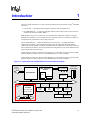
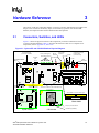
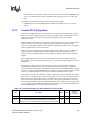
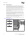
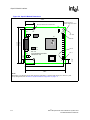
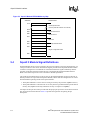
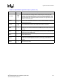
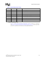
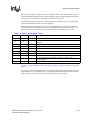
1
i960® Microprocessor User’s
Guide for Cyclone and PCI-SDK
Evaluation Platforms
April 1996
Order Number: 272577-002
Information in this document is provided in connection with Intel products. No license, express or implied, by estoppel or otherwise, to any intellectual
property rights is granted by this document. Except as provided in Intel’s Terms and Conditions of Sale for such products, Intel assumes no liability
whatsoever, and Intel disclaims any express or implied warranty, relating to sale and/or use of Intel products including liability or warranties relating to
fitness for a particular purpose, merchantability, or infringement of any patent, copyright or other intellectual property right. Intel products are not
intended for use in medical, life saving, or life sustaining applications.
Intel may make changes to specifications and product descriptions at any time, without notice.
Contact your local Intel sales office or your distributor to obtain the latest specifications and before placing your product order.
Copies of documents which have an ordering number and are referenced in this document, or other Intel literature may be obtained by calling 1-800548-4725 or by visiting Intel’s website at http://www.intel.com.
Copyright © Intel Corporation, 1996
*Third-party brands and names are the property of their respective owners.
i960® Microprocessor User’s Guide for Cyclone and
PCI-SDK Evaluation Platforms
Contents
1
Introduction ...............................................................................................................1-1
1.1
1.2
1.3
1.4
2
Getting Started .........................................................................................................2-1
2.1
2.2
2.3
2.4
3
Advantages and Features ..................................................................................1-2
About This Manual .............................................................................................1-2
1.2.1 Notation Conventions ............................................................................1-3
Technical Support, Schematics, and PLD Equations.........................................1-3
Additional Information.........................................................................................1-3
Pre-Installation Considerations ..........................................................................2-1
2.1.1 Software Development Tools ................................................................2-1
2.1.2 MON960 Debug Monitor .......................................................................2-1
2.1.3 Host Communications ...........................................................................2-1
2.1.3.1 Terminal Emulation Method .....................................................2-2
2.1.3.2 Host Debugger Interface Library (HDIL) Method......................2-2
2.1.3.3 Source Level Debugger............................................................2-2
2.1.4 Power Requirements .............................................................................2-2
Software Installation ...........................................................................................2-3
2.2.1 Installing Software Development Tools .................................................2-3
Hardware Installation..........................................................................................2-3
2.3.1 Verify Cyclone EP is Functional ............................................................2-3
Creating and Downloading the Example Program .............................................2-4
2.4.1 MONDB.EXE-to-Cyclone EP Communication Support .........................2-4
2.4.2 Terminal Emulation-to-Cyclone EP Communication Support................2-6
Hardware Reference...............................................................................................3-1
3.1
3.2
3.3
3.4
3.5
3.6
3.7
3.8
3.9
3.10
Connectors, Switches, and LEDs.......................................................................3-1
CPU Modules .....................................................................................................3-2
3.2.1 CPU Module Installation ........................................................................3-2
3.2.2 CPU Module Clock Frequencies ...........................................................3-3
3.2.3 i960® Jx/Hx CPU Counter/Timers .........................................................3-3
3.2.4 CPU Module VPP Switch .......................................................................3-3
CPU Memory Map ..............................................................................................3-4
Interleaved DRAM ..............................................................................................3-4
3.4.1 DRAM Performance ..............................................................................3-5
3.4.2 Upgrading SIMM DRAM ........................................................................3-5
Flash Memory.....................................................................................................3-6
3.5.1 SwapROM Switch .................................................................................3-6
Interrupts ............................................................................................................3-7
Console Serial Port ............................................................................................3-8
Parallel Port........................................................................................................3-9
3.8.1 Parallel Port Bit Assignments ................................................................3-9
Z8536 Counter I/O Unit (CIO) ..........................................................................3-10
3.9.1 Counter/Timers....................................................................................3-10
3.9.2 CIO Port A ...........................................................................................3-11
3.9.3 CIO Port B ...........................................................................................3-12
3.9.4 CIO Port C...........................................................................................3-12
Non-Volatile Parameter Memory ......................................................................3-13
i960® Microprocessor User’s Guide for Cyclone and
PCI-SDK Evaluation Platforms
iii
3.11
3.12
4
Theory of Operation ...............................................................................................4-1
4.1
4.2
4.3
4.4
4.5
4.6
4.7
iv
Squall II Module Interface ................................................................................3-13
PLX PCI 9060 Interface (PCI-SDK Platform Only)...........................................3-14
3.12.1 PCI 9060 Configuration .......................................................................3-15
3.12.1.1 Accessing Configuration Registers .......................................3-15
3.12.1.2 PCI-to-Local Configuration ....................................................3-16
3.12.1.3 RAM Region Configuration ...................................................3-18
3.12.1.4 Expansion ROM Region Configuration .................................3-21
3.12.1.5 Memory Region Configuration Examples..............................3-21
3.12.2 Local-to-PCI Configuration ..................................................................3-23
3.12.3 Deadlock Configuration .......................................................................3-26
3.12.4 Signalling Init Done .............................................................................3-27
3.12.5 PCI Interrupts ......................................................................................3-27
3.12.5.1 Local PCI Interrupts ..............................................................3-27
3.12.6 Mailbox Registers and Doorbell Interrupts ..........................................3-29
3.12.6.1 Using the Mailbox Registers..................................................3-29
3.12.6.2 Generating Doorbell Interrupts ..............................................3-30
3.12.6.3 Receiving Doorbell Interrupts ................................................3-30
3.12.7 DMA Programming..............................................................................3-30
3.12.7.1 DMA Non-Chaining Mode .....................................................3-31
3.12.7.2 DMA Chaining Mode .............................................................3-32
3.12.7.3 DMA Interrupts ......................................................................3-33
Functional Overview...........................................................................................4-1
Clock Generation ...............................................................................................4-1
Power Monitor and Reset...................................................................................4-2
I/O Interface .......................................................................................................4-2
4.4.1 Functional Blocks ..................................................................................4-2
4.4.2 I/O Control Timing .................................................................................4-3
4.4.3 Data Path ..............................................................................................4-4
4.4.3.1 Parallel Port..............................................................................4-4
4.4.3.2 Serial Port.................................................................................4-5
DRAM Subsystem ..............................................................................................4-6
4.5.1 Page Mode DRAM SIMM Review .........................................................4-6
4.5.1.1 Bank Interleaving......................................................................4-6
4.5.1.2 Wait State Performance ...........................................................4-7
4.5.2 DRAM Controller Implementation..........................................................4-7
CAS# Generation ...............................................................................................4-9
Refresh Generation ............................................................................................4-9
i960® Microprocessor User’s Guide for Cyclone and
PCI-SDK Evaluation Platforms
5
Squall II Module Interface ....................................................................................5-1
5.1
5.2
5.3
5.4
5.5
5.6
5.7
5.8
5.9
A
Physical Attributes..............................................................................................5-1
Power Requirements..........................................................................................5-3
Squall II Module Serial EEPROM.......................................................................5-3
Squall II Module Signal Definitions.....................................................................5-4
Squall Module Signal Descriptions.....................................................................5-6
Squall II Module Timing......................................................................................5-8
5.6.1 Squall II Module Slave Timing ...............................................................5-8
5.6.2 Squall II Module Master Timing ...........................................................5-12
Squall II Module Connector ..............................................................................5-17
Squall II Module Signal Loading and Logic Selection ......................................5-18
Squall II Module Clock Termination..................................................................5-19
Parts List .................................................................................................................... A-1
Index ...................................................................................................................... Index-1
Figures
1-1
2-1
2-2
3-1
3-2
3-3
3-4
3-5
3-6
3-7
4-1
4-2
4-3
4-4
5-1
5-2
5-3
5-4
5-5
5-6
5-7
5-8
5-9
5-10
Cyclone EP and PCI-SDK Platform Functional Block Diagram..........................1-1
Download Messages ..........................................................................................2-5
Program Execution Messages ...........................................................................2-6
Cyclone EP and PCI-SDK Platform Physical Diagram.......................................3-1
DRAM Memory Map for Cyclone EP..................................................................3-4
CIO Port A ........................................................................................................3-11
CIO Port B ........................................................................................................3-12
CIO Port C........................................................................................................3-13
Non-Chaining DMA Initialization.......................................................................3-31
Chaining DMA Initialization ..............................................................................3-32
I/O Control State Machine ..................................................................................4-3
Parallel Port Timing Signals ...............................................................................4-5
Two-way Interleaving .........................................................................................4-7
DRAM State Machine .........................................................................................4-8
Squall II Module Component Height Allowance .................................................5-1
Squall II Module Dimensions..............................................................................5-2
Squall II Module EEPROM Memory Map ...........................................................5-4
Squall II Slave Read and Write Timing Diagram ..............................................5-10
Squall II Slave Burst Read Timing Diagram .....................................................5-11
Squall II Slave Burst Write Timing Diagram .....................................................5-12
Squall II Master Read and Write Timing Diagram ............................................5-14
Squall II Master Burst Read and Write Timing Diagram...................................5-15
Squall II Master Read Using S_EXTEND#.......................................................5-16
Squall II Module Clock Termination..................................................................5-19
i960® Microprocessor User’s Guide for Cyclone and
PCI-SDK Evaluation Platforms
v
Tables
3-1
3-2
3-3
3-4
3-5
3-6
3-7
3-8
3-9
3-10
3-11
3-12
3-13
3-14
3-15
3-16
3-17
3-18
3-19
3-20
3-21
3-22
3-23
3-24
3-25
3-26
3-27
3-28
3-29
3-30
3-31
3-32
3-33
4-1
5-1
5-2
5-3
5-4
5-5
5-6
5-7
A-1
vi
External Connectors and LEDs ........................................................................3-2
CPU Module Frequency Switch Settings ...........................................................3-3
i960® Jx/Hx CPU Clock Rates ...........................................................................3-3
DRAM Access Times .........................................................................................3-5
DRAM SIMM Configurations ..............................................................................3-6
Flash ROM Addresses .......................................................................................3-6
Interrupt Sources................................................................................................3-7
80960Sx and Kx Interrupt Sources ....................................................................3-7
80960Sx and Kx Interrupt Switch Settings .........................................................3-8
UART Register Addresses .................................................................................3-8
Parallel Port Addresses......................................................................................3-9
Parallel Port Status Register Bit Assignments ...................................................3-9
Parallel Port Control Register Bit Assignments ................................................3-10
CIO Register Address ......................................................................................3-10
CIO Port A Bits 5-3...........................................................................................3-11
CIO Port A Bits 2-0...........................................................................................3-11
Available Squall II Modules ..............................................................................3-14
Squall Module Compatibility at Maximum CPU Clock Speed (33 MHz) ..........3-14
Local Configuration Registers ..........................................................................3-17
PCI Configuration Registers.............................................................................3-18
Memory Region 0 Settings ...............................................................................3-19
Local Address Space 0 Range Register ..........................................................3-19
Local Address Space 0 Local Base Address (Re-map)
Register Description .........................................................................................3-19
Local Bus Region Descriptor for PCI-to-Local Access
Register Description .........................................................................................3-20
ROM Region Settings ......................................................................................3-21
Local Expansion ROM Local Base Address (Re-map) and BREQo
Register Description .........................................................................................3-22
Local Expansion ROM Range Register Description ........................................3-22
Local Range Register for Direct Master-to-PCI Description.............................3-23
PCI Base Address (Re-map) Register for Direct Master-to-PCI
Description .......................................................................................................3-24
Local Bus Base Address Register for Direct Master-to-PCI Memory...............3-25
Local Base Address for Direct Master-to-PCI IO/CFG Register ......................3-25
PCI Configuration Address Register for Direct Master-to-PCI IO/CFG ............3-25
Interrupt Control/Status ....................................................................................3-28
DRAM Profiles....................................................................................................4-8
Power Supply .....................................................................................................5-3
Pin Description Nomenclature............................................................................5-5
Squall Module Signal Descriptions.....................................................................5-6
Squall II Module Slave Timing............................................................................5-9
Squall II Module Master Timing........................................................................5-13
Squall II Module Pin Assignments....................................................................5-17
Squall II Module Signal Loading.......................................................................5-18
Cyclone EP/PCI-SDK Platform Bill Of Materials ............................................... A-1
i960® Microprocessor User’s Guide for Cyclone and
PCI-SDK Evaluation Platforms
1
Introduction
This user’s guide describes the Cyclone evaluation platforms for Intel’s family of i960® embedded
processors:
• Cyclone EP — a standalone general purpose evaluation and development tool.
• PCI-SDK Platform — Cyclone EP equipped with a PCI bus interface. Part of Intel’s PCI I/O
Software Development Toolkit (SDK).
Both platforms allow you to connect one of several i960 CPU and Squall* modules. Using the
different CPU modules, you can evaluate the various i960 processors in a system environment, or
“benchmark” the performance of the various processors.
The PCI-SDK Platform — otherwise identical to the Cyclone EP — is equipped with PLX
Technology’s PCI 9060 (a PCI to 80960 bus bridge chip). The single-chip PCI 9060 features
mailbox and doorbell registers that allow command and status information to pass between PCI bus
devices and local bus devices. It can also generate PCI configuration cycles, which enables the PCI
9060 to become the PCI system host.
Unless otherwise noted, all references in this manual to “Cyclone EP” also apply to the PCI-SDK
Platform. References that are specific to PCI-SDK Platform are clearly indicated.
Unless otherwise noted, all references in this manual to “Cyclone EP” also apply to the PCI-SDK
Platform. References that are specific to PCI-SDK Platform are clearly indicated.
Figure 1-1. Cyclone EP and PCI-SDK Platform Functional Block Diagram
To
I/O Panel
Connector
i960® Processor
Module
Clock Distribution
Interleaved
DRAM SIMMs
Squall Module
CPU
Flash ROM
DRAM Control
Local Bus
PCI-SDK
ONLY
PLX 9060
®
PCI to i960 CPU
Bridge with DMA
CIO
Counter /
Timers
Expansion
Flash
ROM
Parallel
Download
Port
UART Based
RS-232
Serial Port
DB-25 Connector
Phone Jack
Connection
PCI Bus
i960® Microprocessor User’s Guide for Cyclone and
PCI-SDK Evaluation Platforms
1-1
Introduction
1.1
Advantages and Features
As shown in Figure 1-1 and Figure 3-1 “Cyclone EP and PCI-SDK Platform Physical Diagram,”
the features which make the Cyclone EP useful for evaluation and code development are:
• Interchangeable i960 processor modules
(referred to as CPU modules)
• SIMM sockets which support 2, 8, or 32
Mbytes of DRAM
• DIP switch selectable processor clock
frequency
• DRAM controller automatically optimizes
wait states to CPU frequency and memory
speed
• Flash ROM sockets
• Three 16-bit counter/timers or one 32-bit
and one 16-bit counter
• Squall II Module I/O expansion interface
• RS-232 serial port
• Parallel download port (Centronics
compatible)
• PCI Bus Interface (PCI-SDK Platform
only)
1.2
About This Manual
This manual contains five chapters, one appendix and an index. A brief description of each
follows:
Chapter 1,
“Introduction”
Introduces Intel’s Cyclone Evaluation Platform and its features. Also
defines notation conventions and related documentation.
Chapter 2, “Getting
Started”
In this chapter, step-by-step instructions show you how to connect the
Cyclone EP to a power supply and download and execute an example
program. This chapter describes Intel’s software development tools, the
MON960 Debug Monitor, software installation and hardware
configuration.
Chapter 3,
“Hardware
Reference”
The location of the CPU and Squall modules, connectors, switches, and
LEDs are described in this chapter. Also covered are the memory maps,
I/O and memory operation. For the PCI-SDK Platform, this chapter
describes the PCI 9060 interface and operation.
Chapter 4, “Theory
of Operation”
This chapter describes functionality of the Cyclone Evaluation
Platform’s subsystems. “I/O Interface” describes the general I/O
implementation. Subsections further describe each functional block.
“DRAM Subsystem” similarly defines the DRAM implementation. Also
covered are Clock Generation, Reset, Interrupt and Ready Logic.
Chapter 5, “Squall
Design information, electrical and physical specifications of the Squall
II Module Interface” II Module interface are described in this chapter. This information is
useful when you wish to design and integrate your own Squall Modules.
If you are using a standard Squall Module, refer to the specific module’s
manual for information on the operation of that module.
Appendix A, “Parts
List”
1-2
This appendix identifies Cyclone Evaluation Platform components and
quantities, component reference name as it appears on the PC board,
description of size or rating and the manufacturer’s part number. To
order replacement parts contact the manufacturer listed in Table A-1.
i960® Microprocessor User’s Guide for Cyclone and
PCI-SDK Evaluation Platforms
Introduction
1.2.1
1.3
Notation Conventions
Hexadecimal Numbers
In text, hexadecimal numbers are shown with a suffix of “H” (e.g., XXXX XXXXH).
In code examples and PLD files, and in text that refers to specific code examples,
hex numbers are shown with a prefix of “0x” (e.g., 0xXXXXXXXX).
#
Inverted clock signals are indicated with a trailing pound sign (RAS#).
Bold
Indicates user entry and/or commands.
Italics
Indicates a reference to related documents; also used to show emphasis.
typewriter font
Indicates code examples and file directories and names.
asterisks
On non-Intel company and product names, a trailing asterisk indicates the item is a
trademark or registered trademark. Such brands and names are the property of
their respective owners.
Technical Support, Schematics, and PLD Equations
For Technical assistance with the Cyclone EP, contact the Intel Technical Support Hotline. For
information about technical support in other geographical areas, contact Intel’s North America
Technical Support Hotline.
You can also use your PC with modem to download Cyclone EP and PCI-SDK Platform
schematics and PLD equations from Intel’s Bulletin Board Service (BBS).
North America: 800-628-8686
Intel Technical Support Hotline
Europe: 44-793-696-000
North America: 916-356-3600
supports up to 14.4 Kbps (n,8,1,p)
Intel’s Bulletin Board Service (BBS)
for schematics and PLD equations
Europe: 44-793-432-955
1.4
Additional Information
To order manuals from Intel, contact your local sales representative or Intel Literature Sales
(1-800-879-4683).
Product
All
80960Cx
80960Jx
Document Name
Company /
Order Number
Intel Solutions960® catalog
Intel 270791
i960®
Intel 270710
Cx Microprocessor User’s Manual
80960CA-33, -25, -16 32-Bit High Performance Embedded Processor Data Sheet
Intel 270727
80960CF-33, -25, -16 32-Bit High Performance Superscalar Processor Data
Sheet
Intel 272187
80960CF-40 32-Bit High Performance Superscalar Processor Data Sheet
Intel 272493
i960® Jx Microprocessor User’s Manual
Intel 272483
80960JA/JF Embedded 32-Bit Microprocessor Data Sheet
Intel 272504
i960® Microprocessor User’s Guide for Cyclone and
PCI-SDK Evaluation Platforms
1-3
Introduction
Product
80960Kx
80960Sx
Document Name
i960® KA/KB Microprocessor Programmer’s Reference Manual
Intel 270567
80960KB Hardware Designer’s Reference Manual
Intel 270564
80960KA Embedded 32-Bit Processor Data Sheet
Intel 270775
80960KB Embedded 32-Bit Processor With Integrated Floating Point Unit Data
Sheet
Intel 270565
i960® SA/SB Microprocessor Reference Manual
Intel 270929
80960SA Embedded 32-Bit Processor With 16-Bit Burst Data Bus Data Sheet
Intel 272206
80960SB Embedded 32-Bit Processor With 16-Bit Burst Data Bus and Integrated
Floating Point Unit Data Sheet
Intel 272207
MON960 Debug Monitor User’s Guide
Intel 484290
Z8536 CIO Counter/Timer Technical Manual
Zilog, Inc.
Texas
Instruments
16C550 Data Sheet
Other
Company /
Order Number
24C08 Serial EEPROM Data Sheet
Xicor, Inc.
Data Communications Local Area Networks UARTs Handbook
National
Semiconductor
PCI 9060 User’s Guide / Data Sheet
PLX
Technology
(800-759-3735)
To contact Cyclone Microsystems for additional information about their products:
Cyclone Microsystems
25 Science Park
New Haven CT 06511
1-4
Phone: 203-786-5536
FAX: 203-786-5025
e-mail: [email protected]
i960® Microprocessor User’s Guide for Cyclone and
PCI-SDK Evaluation Platforms
Getting Started
2
In this chapter, step-by-step instructions show you how to connect the Cyclone EP to a power
supply and download and execute an example program. This chapter describes Intel’s software
development tools, the MON960 Debug Monitor, software installation and hardware configuration.
2.1
Pre-Installation Considerations
This section provides a general overview of the components required to develop and execute a
program on the Cyclone EP. The MON960 Debug Monitor User’s Guide (order number 484290)
fully describes several of these components, including MON960 commands, Host Debugger
Interface Library (HDIL) and the MONDB.EXE utility.
2.1.1
Software Development Tools
The Cyclone EP supports many software development tools1. The installation instructions
presented in this chapter were verified using GNU/960 and CTOOLS960 — Intel’s i960®
processor software development tools. Advanced C-language compilers for the i960 processor
family are available for DOS-based systems and a variety of UNIX workstation hosts. These
products provide execution profiling and instruction scheduling optimizations and also provide an
assembler, linker and utilities designed for embedded processor software development.
The instructions in this section explain how to compile, link and execute an example program. If
you are using other software development tools, read through this example to gain a general
understanding of how to use your tools with this board.
2.1.2
MON960 Debug Monitor
The Cyclone EP is equipped with Intel’s MON960 — an on-board software monitor which allows
you to execute and debug programs written for i960 processors. The monitor provides program
download, breakpoint, single step, memory display and other useful functions for running and
debugging a program.
The Cyclone EP works with source-level debuggers, such as the DB960 and GDB960. The sourcelevel debugger must support the Host Debugger Interface Library (HDIL) defined by MON960.
2.1.3
Host Communications
MON960 allows you to communicate and download programs developed for the Cyclone EP
across a PC’s serial, parallel, or PCI interface and a UNIX workstation’s serial interface. The
Cyclone EP supports two methods: Terminal emulation and Host Debugger Interface Library
(HDIL).
1.
Refer to Intel’s Solutions960® catalog for a complete list of i960 processor software development and debug tools.
i960® Microprocessor User’s Guide for Cyclone and
PCI-SDK Evaluation Platforms
2-1
Getting Started
2.1.3.1
Terminal Emulation Method
Terminal emulation software on your system communicates to MON960 on the Cyclone EP via an
RS-232 serial port. Serial downloads via terminal emulation require an intelligent host computer
that supports XMODEM (a standard transfer protocol). General system requirements are:
• DOS-based computer with PROCOMM*, CROSSTALK* or other telecommunication
programs
• UNIX* workstation with an external serial port (e.g., SUN*)
Configure the serial port for 1200-115200 baud, 8 bits, one stop bit, no parity.
2.1.3.2
Host Debugger Interface Library (HDIL) Method
The MONDB.EXE utility, provided with MON960, allows you to download, execute and debug an
application program on the Cyclone EP. This utility differs from standard terminal emulation
programs in that it allows you to download executable images through a serial or parallel port, or
via the PCI bus. When using the serial port, the MONDB.EXE utility supports the standard baud
rates (from 1200 to 115200 baud) to communicate and download to the Cyclone EP. Downloading
via either the parallel port or PCI bus is typically much faster than a serial port; actual performance
depends on your system’s hardware capabilities. Refer to MON960 Debug Monitor User’s Guide
for detailed information.
2.1.3.3
Source Level Debugger
You may use a source-level debugger, such as Intel’s DB960, GDB960 or other, to establish serial
communications with the Cyclone EP. The MON960 Host Debugger Interface Library (HDIL)
provides the interface between MON960 and these types of debuggers.
2.1.4
Power Requirements
The Cyclone EP requires a stable power source of at least 3.5 A at +5 VDC. The included power
supply meets these requirements and connects to J7. If a card is designed for the expansion bus
which requires more than 1.0 A, you need to obtain a suitable power supply. To program FLASH
devices, you must supply a FLASH programming voltage through J6. J6 uses a standard PC-AT
power connector pinout that provides +5 VDC and +12 VDC to the board. J7 provides +5 VDC
only. See Figure 3-1 “Cyclone EP and PCI-SDK Platform Physical Diagram” on page 3-1, for J6,
J7 locations.
The PCI-SDK Platform draws power from the PCI bus; it does not require an external power
source. The PCI bus also provides the voltages needed for FLASH programming.
2-2
i960® Microprocessor User’s Guide for Cyclone and
PCI-SDK Evaluation Platforms
Getting Started
2.2
Software Installation
2.2.1
Installing Software Development Tools
If you haven’t done so already, install your development software (CTOOLS960, GNU/960 or
other) as described in their respective manuals. All further references to CTOOLS960 or GNU/960
assume the default directories in the respective installation program were selected. You must install
the tools before you run the example program as described in Section 2.4, “Creating and
Downloading the Example Program” on page 2-4.
The example program provided on the MON960 diskette enables you to use CTOOLS960 or GNU/
960 (or other) to compile a sample application program. If you are using other software tools, these
instructions generally apply; however, in some steps you will need to refer to their respective
manuals for compatible commands.
2.3
Hardware Installation
Follow these instructions to get your new Cyclone EP running. Be sure you have all items listed on
the checklist provided with your Cyclone Evaluation Platform.
2.3.1
Warning:
Verify Cyclone EP is Functional
MAKE SURE YOU ARE GROUNDED BEFORE REMOVING THE ANTI-STATIC BAG.
OTHERWISE, SEVERE DAMAGE MAY OCCUR TO THE BOARD.
1. Visually inspect the board for any damage that may have occurred during shipment. If there
are visible defects, return the board for replacement.
2. Place the board in a static-free area; always take precautions to minimize static electricity.
3. Verify that an i960 processor module is installed.
4. Verify that the SwapROM switch (S1 position 3) DIP switch is set to OFF.
5. To install the PCI-SDK Platform in a host system PCI slot, follow the manufacturer’s
instructions for opening the host system and installing an expansion board in a PCI slot.
6. Serial port connection for communicating and downloading: connect the RS-232 cable — the
“phone cord” — from an appropriate port (COM1 or COM2 on a PC) to J5 on the Cyclone EP.
Your system has either a DB-9 (9-pin) or a DB-25 (25-pin) connector for its RS-232 port. Both
9-pin and 25-pin connectors are provided.
7. Parallel port connection (optional if using MONDB.EXE) for downloading: connect a 25-pin
to 25-pin parallel port cable from an appropriate port (LPT1 or LPT2 on a PC) to J1 on the
Cyclone EP.
8. Power supply connections (not required for the PCI-SDK Platform): the Cyclone EP has two
power connectors: J6 and J7. Refer to Section 2.1.4, “Power Requirements” on page 2-2 for a
description of these connectors; see Figure 3-1 “Cyclone EP and PCI-SDK Platform Physical
Diagram” on page 3-1 to verify locations.
i960® Microprocessor User’s Guide for Cyclone and
PCI-SDK Evaluation Platforms
2-3
Getting Started
Warning:
FAILURE TO PROPERLY CONNECT THE POWER CABLE COULD RESULT IN SEVERE
DAMAGE TO THE BOARD.
If using the power supply provided with the Cyclone EP, plug the power supply cable into
connector J7. The power supply operates with 120 VAC @ 60 Hz.
If using a power supply that provides +5 VDC, +12 VDC and ground (supply not provided),
plug the power supply cable into connector J6.
The PCI-SDK Platform draws power from the PCI bus and should not be connected to an
external power supply.
9. Check for power within tolerance. The +5V and +3.3V LEDs should be lit. The -12V and
+12V power sources are optional on the standalone board, but should be lit when a PCI-SDK
Platform is installed in a PCI slot.
Upon power up the Fail LED should turn OFF, indicating the processor has passed its self test.
The green Run LED should light, indicating that the processor is performing bus cycles.
2.4
Creating and Downloading the Example Program
When you install MON960 on DOS, a text file (ZZ\EXAMPLE\CYCLONE\IMAGE.TXT)
describes how to compile, assemble and link the example program. The text file describes how to
create the executable image. For this example, the image file is named SIEVE.XX (“XX” is either
Cx, Hx, Jx, Kx, or Sx, depending on which CPU module you are using).
If you are using MONDB.EXE on DOS to communicate with the Cyclone EP, continue to
Section 2.4.1. If using a terminal emulation program, proceed to Section 2.4.2, “Terminal
Emulation-to-Cyclone EP Communication Support” on page 2-6.
2.4.1
MONDB.EXE-to-Cyclone EP Communication Support
To invoke the MONDB.EXE utility and download your application program: make sure you are in
the ..\CYCLONE directory and, at the DOS prompt, enter DWNLD followed by the name of the
image file (filename is not case sensitive). For example, for the Cx CPU module, enter:
DWNLD SIEVE.CX
DWNLD invokes a batch file (DWNLD.BAT) which contains MONDB.EXE commands which
configure serial port 1, parallel port 1, and set the baud rate to 19200. You can use a text editor to
modify this batch file such that it is correct for your system’s configuration. Refer to MON960
Debug Monitor User’s Guide for a description of all commands.
Figure 2-1 shows the messages that display during the download. If using the serial port, the
download time increases depending on the baud rate.
2-4
i960® Microprocessor User’s Guide for Cyclone and
PCI-SDK Evaluation Platforms
Getting Started
Figure 2-1. Download Messages
Section 0, name .text, address 0xA0008000, size 0x6a9c, flags 0x20
writing section at 0xA0008000
Section 1, name .data, address 0xA000ea9c, size 0x4, flags 0x40
writing section at 0xA000ea9c
Section 2, name .bss, address 0xA000ea90, size 0x6d0, flags 0x80 -- noload
Download stats 0.050 sec elapsed, 545920 bytes/sec (533.3Kb/sec)
Starting execution at 0xA0008000 use CTRL-C to interrupt.
>>> Start of sieves test. <<<
Sieve of Eratosthenes (scaled to 10 Iterations)
Array Size
(Bytes)
8191
10000
20000
40000
80000
160000
Primes
Found
1899
2261
4202
7836
14683
27607
Last Prime
16381
19997
39989
79999
160001
319993
BenchTime
(Sec)
0.060
0.073
0.149
0.301
0.610
1.235
Relative to 10 Iterations and the 8191 Array Size:
Average BenchTime =
0.060 (sec)
>>> End of sieves test. <<<
Program Exit: 0
i960® Microprocessor User’s Guide for Cyclone and
PCI-SDK Evaluation Platforms
2-5
Getting Started
2.4.2
Terminal Emulation-to-Cyclone EP Communication Support
1. Invoke the terminal emulation program that you are using to communicate with the Cyclone
EP.
2. To establish communication between the terminal emulation program and MON960, press
<ENTER>. The MON960 prompt should appear. If it does not, press the RESET button.
3. When the MON960 prompt appears, enter do to download:
=>
do
4. Start your terminal emulation program transfer mode and send SIEVE.XX. The following
message displays when transfer completes:
-- Download complete -Start address is: XXXXXXX=>
5. To execute your program: at the MON960 prompt, enter go:
=> go
(go = go from start or continue from breakpoint)
The messages in Figure 2-2 display when the program completes (times may vary slightly). The
example program has now been successfully compiled, assembled, linked, downloaded and
executed.
Figure 2-2. Program Execution Messages
>>> Start of sieves test. <<<
Sieve of Eratosthenes (scaled to 10 Iterations)
Array Size
(Bytes)
8191
10000
20000
40000
80000
160000
Primes
Found
1899
2261
4202
7836
14683
27607
Last Prime
16381
19997
39989
79999
160001
319993
BenchTime
(Sec)
0.060
0.073
0.149
0.301
0.610
1.235
Relative to 10 Iterations and the 8191 Array Size:
Average BenchTime =
0.061 (sec)
>>> End of sieves test. <<<
Program Exit: 0
=>
2-6
i960® Microprocessor User’s Guide for Cyclone and
PCI-SDK Evaluation Platforms
3
Hardware Reference
The location of the CPU and Squall modules, connectors, switches, and LEDs are described in this
chapter. Also covered are the memory maps, I/O and memory operation. For the PCI-SDK
Platform, this chapter describes the PCI 9060 interface and operation.
3.1
Connectors, Switches, and LEDs
Figure 3-1 shows the physical location of the components you need to understand to use the
Cyclone Evaluation Platform; Table 3-1 describes the function of each. For a complete list of
components, refer to Appendix A, “Parts List”.
Figure 3-1. Cyclone EP and PCI-SDK Platform Physical Diagram
25-Pin Parallel Port
(Centronics compatible)
Four-Position
DIP Switch
RS-232
Serial Port
Bus Cycle LED (green)
Power LEDs (green)
Fail LED (red)
User LEDs
(red)
PCI-SDK Platform
ONLY
GND
0123
+5V
+12V -12V
Reset
Pushbutton
CR6
J5
1 23 4
O FF
CR1 CR2 CR3 CR4
J2
+5 VDC
+3.3V
CR5
CR9
J1
Connectors for external
Power Supplies
(Cyclone EP Only)
+12 VDC
+5 VDC
J6
S1
J7
S2
U20
U19
PLX
PCI 9060
J4
J3
Connect this edge connector
to your system’s PCI slot
flip squall module over
and attach connectors
U1
Z1
J2
U2
Flash Memory
connectors on bottom of CPU module attach here
Xx Processor Module
CYCLONE MICROSYSTEMS
COPYRIGHT 1994
© 19xx
M
i
i960®
x80960xx-00
XXXXXXXX A0
attach SIMMs in connectors at 45° angle
U4
U3
Z2
123-1234-12
Rev. xxxx
CYCLONE MICROSYSTEMS
COPYRIGHT 1995
SW1
DRAM SIMM
1 234
U5
OFF
Frequency and VPP switches
Squall II Module
i960® Microprocessor User’s Guide for Cyclone and
PCI-SDK Evaluation Platforms
CPU Module
Flash Memory (MON960)
3-1
Hardware Reference
Table 3-1. External Connectors and LEDs
Function
Ref.
Power +5 VDC
(Cyclone EP only)
J7
Description
A one-pin connector that interfaces to the primary power supply and cable
(supplied). Provides +5 VDC and ground connections.
(On the PCI-SDK Platform, power is supplied through the edge connector.)
Power +5 VDC, +12 VDC
(Cyclone EP only)
J6
A four-pin connector that interfaces to a secondary power supply and cable (not
supplied). Three of the connector pins connect to +5 VDC, +12 VDC and ground.
(On the PCI-SDK Platform, power is supplied through the edge connector.)
LED (GREEN)
CR1
CR2
CR3
CR4
CR5
Lit when +5V is in tolerance
Lit when +12V is in tolerance
Lit when -12V is in tolerance
Lit when +3.3V and +5V is in tolerance
Lit when processor is performing bus cycles.
LED (RED)
CR6
Lit if processor fails self test or CPU module is not installed.
User LEDs (RED)
CR9
Four user-programmable LEDs; programmed via CIO Port C.
Serial Port (RS-232)
J5
An RJ-11 (“phone plug”) connector for serial communication and download.
Parallel Port
(Centronics-compatible)
J1
A DB-25 connector for parallel download.
Squall II Interface
J2
Allows Squall II Module expansion. I/O devices are given direct access to the
memory system.
J3, J4
Modules which allow all current and future i960 processors to be used on the
Cyclone EP and PCI-SDK Platform.
i960 Processor Module
(CPU Module)
S1.1 Enables VPP to Cyclone EP base board Flash ROMs
S1.2 Enables UART Interrupt Request to the NMI
Four-position DIP Switch
S1
S1.3 ROMSWAP - causes the addresses of the CPU Module ROM and the base
board ROMs to be exchanged. If switch is OFF the processor boots from the
CPU Module ROM. If switch is ON the processor boots from base board ROMs.
Reset pushbutton
S2
DRAM SIMM Sockets
3.2
U19-U20
Used to manually reset the Cyclone EP.
Supports up to 32 Mbytes of standard 72-pin SIMMs.
CPU Modules
As shown in Figure 3-1, a CPU module is a smaller board that attaches directly onto the Cyclone
EP. Several CPU modules are available — one for each member of the i960 processor family. Each
module contains a i960 processor, boot Flash ROM with the MON960 monitor, appropriate glue
logic and configuration switches.
3.2.1
CPU Module Installation
CPU modules are easy to install when a few guidelines are observed:
• Make sure the power is OFF before you install or remove a CPU module.
• Do not “peel” connectors. Peeling is the action of lifting one end of the connector before the
other. This can bend or break the pins and connectors.
3-2
i960® Microprocessor User’s Guide for Cyclone and
PCI-SDK Evaluation Platforms
Hardware Reference
3.2.2
CPU Module Clock Frequencies
The CPU modules have user-assignable clock frequencies. Make sure you do NOT select a
frequency faster than the installed processor is capable of running. Table 3-2 outlines the processor
frequency switch settings. It is recommended that you remove power before you change the switch
settings; however, if you change the switch settings while power is connected, press the reset
switch to reboot the processor at the new frequency.
Note:
DO NOT select a frequency faster than the installed processor is capable of running.
Table 3-2. CPU Module Frequency Switch Settings
FREQ2
(Pos2)
FREQ1
(Pos3)
FREQ0
(Pos4)
16 MHz
ON
OFF
ON
20 MHz
ON
OFF
OFF
25 MHz
OFF
ON
ON
33 MHz
OFF
ON
OFF
40 MHz
OFF
OFF
ON
50 MHz
OFF
OFF
OFF
Switch Diagram1,2
1
2 3 4
DHS-4
Frequency
OFF
NOTES:
1. On the 80960Sx and Kx CPU Modules, the CPU Module Frequency Switch is labeled SW2. On all other
80960 CPU Modules, the CPU Module Frequency Switch is labeled SW1.
2. CPU module switch position 1 (Pos1) is the VPP switch. It is recommended that you leave it OFF. (Factory
default position.)
3.2.3
i960® Jx/Hx CPU Counter/Timers
The i960 Jx and Hx processors are equipped with two on-chip counter/timers. These timers are
clocked at the CPU clock rate which does not correspond exactly with the CPU Module Frequency
Switch settings. Use Table 3-3 to determine the exact CPU clock frequency.
Table 3-3. i960® Jx/Hx CPU Clock Rates
CPU Frequency
Switch Setting
3.2.4
CPU Clock Frequency
16 MHz
16.11 MHz
20 MHz
20.05 MHz
25 MHz
25.06 MHz
33 MHz
33.41 MHz
40 MHz
40.09 MHz
CPU Module VPP Switch
The VPP Switch (switch position 1 in Table 3-2) enables/disables VPP to the boot Flash ROMs
located on the CPU module. It is recommended that this switch remain set to OFF (the default
setting from the factory). When VPP is enabled (switch in ON position), the processor may not be
able to boot from ROM if the power sequencing of +5V and +12V is not correct.
i960® Microprocessor User’s Guide for Cyclone and
PCI-SDK Evaluation Platforms
3-3
Hardware Reference
3.3
CPU Memory Map
As indicated in Figure 3-2, the memory map is organized to take advantage of the i960 Cx, Hx, and
Jx processors’ bus sizing capabilities. Memories and I/O devices are described in the sections
following the figure.
Figure 3-2. DRAM Memory Map for Cyclone EP
F000 0000H
CPU Module Flash Boot ROM
for 80960Cx / Jx / Hx
EFFF FFFFH
Expansion Flash ROM
E000 0000H
Expansion Flash ROM
Reserved
D000 0000H
Squall Module
C000 0000H
B00C 0000H
Reserved
B008 0000H
Parallel Port
B004 0000H
CIO
B000 0000H
Serial Port
DRAM
E004 0000H
Flash Socket 1 (U27)
E000 0000H
Flash Socket 2 (U22)
A000 0000H
Reserved
8000 0000H
4000 0000H
PLX PCI 9060
(PCI - SDK only)
PCI Bus
(PCI - SDK only)
CPU Module Flash Boot ROM
0000 0000H
3.4
for 80960Kx / Sx
Interleaved DRAM
The Cyclone EP is initially configured with 2 Mbytes of interleaved DRAM. This memory, located
in the SIMM sockets, is upgradeable to 8 or 32 Mbytes. Figure 3-1 on page 3-1 shows the SIMMs
and sockets. Section 3.4.2 discusses the DRAM configuration options.
Access to this DRAM can be shared with the Squall II Module I/O device’s DMA controller. A
priority arbitration circuit ensures that only one device is using the memory at a time.
3-4
i960® Microprocessor User’s Guide for Cyclone and
PCI-SDK Evaluation Platforms
Hardware Reference
3.4.1
DRAM Performance
The DRAM controller automatically adjusts wait states based on processor type, processor clock
frequency, and memory speed. The controller supports burst transfers using the interleaved banks
to maximize performance. Table 3-4 lists DRAM performance.
The default memory configuration uses 70 ns memory. At processor frequencies of 25 and
40 MHz, wait states are reduced using 60 ns memory.
Table 3-4. DRAM Access Times
Frequency
Operation
DRAM Speed
Clock Cycles
Wait States
Sustained
Bandwidth1
16 MHz
Read
60, 70ns
3,1,1,1
1,0,0,0
36 Mbytes/sec
20 MHz
Read
60, 70ns
3,1,1,1
1,0,0,0
45 Mbytes/sec
25 MHz
Read
60ns
3,1,1,1
1,0,0,0
66 Mbytes/sec
25 MHz
Read
70ns
4,1,1,1,12
2,0,0,0
50 Mbytes/sec
2
33 MHz
Read
60, 70ns
4,1,1,1,1
2,0,0,0
66 Mbytes/sec
40 MHz
Read
60ns
4,1,1,1,12
2,0,0,0
80 Mbytes/sec
2
3,1,1,1
53 Mbytes/sec
1,1,1,1
25.6 Mbytes/sec
40 MHz
Read
70ns
5,2,2,2,1
16 MHz
Write
60, 70ns
3,2,2,2
20 MHz
Write
60, 70ns
3,2,2,2
1,1,1,1
32 Mbytes/sec
25 MHz
Write
60ns
3,2,2,2
1,1,1,1
44.5 Mbytes/sec
25 MHz
Write
70ns
4,2,2,2,12
2,1,1,1
36 Mbytes/sec
33 MHz
Write
60, 70ns
4,2,2,2,12
2,1,1,1
48 Mbytes/sec
2
2,1,1,1
58 Mbytes/sec
2,1,1,1
58 Mbytes/sec
40 MHz
Write
60ns
4,2,2,2,1
40 MHz
Write
70ns
4,2,2,2,12
NOTES:
1. Bandwidths stated are sustained bandwidths, not peak.
2. The extra cycle is the overhead of DRAM precharge. DRAM precharge time only impacts back-to-back cycles.
3.4.2
Upgrading SIMM DRAM
On-board DRAM is located in two SIMM sockets as shown in Figure 3-1. The standard
configuration is 2 Mbytes of memory and may be upgraded to 8 or 32 Mbytes. Table 3-5 shows the
modules which you may use. The memory modules should use 60 or 70 ns Fast Page Mode DRAM
(60 ns memory results in better performance at 25 and 40 MHz operation). Use fast page mode,
x32 or x36, 72 pin SIMMs.
The SIMM block consists of two standard 72-pin SIMM sockets, arranged as two banks. Both
SIMM sockets must contain SIMMs; these cannot be left empty. The sockets accept the following
SIMM types.
• 256 Kbyte x 32 = 1 Mbyte
• 1 Mbyte x 32 = 4 Mbyte
• 4 Mbyte x 32 = 16 Mbyte
• 256 Kbyte x 36 = 1 Mbyte
• 1 Mbyte x 36 = 4 Mbyte
• 4 Mbyte x 36 = 16 Mbyte
i960® Microprocessor User’s Guide for Cyclone and
PCI-SDK Evaluation Platforms
3-5
Hardware Reference
The x36 SIMM parity bits are not used in this design. However, the x36 SIMMs are standard for
PCs and workstations, which makes them more readily available. The only penalty is more loading
on the address and control lines due to the extra DRAM devices on the x36 SIMM.
All address and control lines to the SIMMs are terminated with 22 ohm resistors.
Table 3-5. DRAM SIMM Configurations
Note:
Total Memory (both modules)
Module Type
2 Mbytes
256K x 32 (1 Mbyte)
8 Mbytes
1M x 32 (4 Mbytes)
32 Mbytes
4M x 32 (16 Mbytes)
Both SIMM modules must be installed; SIMM sockets cannot be empty.
The board has no shunts or switches to change for a memory upgrade. Memory speed is indicated
by the Presence Detect Signals; the DRAM controller automatically adjusts to minimum wait states
for the processor frequency and memory speeds. The initialization code automatically sizes the
memory so user software can take advantage of larger memory modules.
3.5
Flash Memory
The Cyclone EP provides two banks of Flash memory: a primary memory bank on the CPU
module and an expansion bank on the base board. The default configuration of this memory is as
the boot memory containing the MON960 monitor. The second bank of memory is two sockets for
Intel 28F020 devices (Intel part number N28F020-200) in locations U22 and U27. These memory
devices may be used for user application code, or using the SwapROM switch, as boot memory.
3.5.1
SwapROM Switch
The SwapROM switch (third switch on SW1) exchanges the addresses of the CPU module boot
ROM and the expansion ROMs to allow the processor to boot from the expansion ROM. Table 3-6
shows the address of the Flash ROMs relative to the SwapROM switch. Figure 3-1 shows SW1
switch location.
Note:
This feature is supported for all i960 processors except for Kx and Sx processors. These must boot
from boot ROMs and, therefore, must have the SwapROM switch set to OFF.
Table 3-6. Flash ROM Addresses
ROM Type
SwapROM Switch OFF
SwapROM Switch ON
CPU Module Boot ROM
F000 0000H
E000 0000H
Expansion ROM0 (U22)
E000 0000H
F000 0000H
Expansion ROM1 (U27)
E004 0000H
F004 0000H
If a single Expansion ROM is used as a Boot ROM, use location U27 (ROM1) so the i960
processor finds the IBR at the top of the memory map.
3-6
i960® Microprocessor User’s Guide for Cyclone and
PCI-SDK Evaluation Platforms
Hardware Reference
3.6
Interrupts
The Cyclone EP has seven interrupt sources. The CPU module assumes the interrupts are direct
mapped. Table 3-7 lists the interrupt sources and the corresponding XINT# signals. All interrupts
are level sensitive except the Squall II Module IRQ0 and IRQ1; these are dependent on the
particular Squall II Module installed.
Table 3-7. Interrupt Sources
XINT Signal
Interrupt Source
XINT0#
PLX PCI 9060
XINT1#
Parallel Port
XINT2#
PCI 9060 LSERR#
XINT3#
Deadlock Error
XINT4#
Squall II Module IRQ0
XINT5#
Squall II Module IRQ1
XINT6#
Counter/Timers (Z8536)
XINT7#
Serial Port (16C550)
The Sx and Kx processors have only four dedicated interrupt signals. A dip switch is provided on
the Sx and Kx CPU modules to map the six possible interrupt sources to the four direct mapped
interrupt inputs. Table 3-8 outlines the interrupt mapping for the Sx and Kx CPU modules.
The interrupt sources to INT1 and INT2 are selected using SW-1 on Sx and Kx modules. Table 3-9
shows all valid combinations. Positions 1 and 2 select the interrupt source to INT1 and both cannot
be ON or OFF simultaneously. Likewise, positions 3 and 4 select the interrupt source to INT2 and
both cannot be ON or OFF simultaneously.
Table 3-8. 80960Sx and Kx Interrupt Sources
INT Signal
Interrupt Source
INT0
Counter/Timers (Z8536)
INT1
Serial Port UART (16C550) or Squall II Module IRQ1
INT2
Parallel Port or PLX PCI 9060
INT3
Squall II Module IRQ0
i960® Microprocessor User’s Guide for Cyclone and
PCI-SDK Evaluation Platforms
3-7
Hardware Reference
Table 3-9. 80960Sx and Kx Interrupt Switch Settings
Pos1
Pos2
Pos3
Pos4
Serial Port UART
PLX PCI 9060
ON†
OFF†
OFF†
ON†
Squall II Module
IRQ1
PLX PCI 9060
OFF
ON
OFF†
ON†
Serial Port UART
Parallel Port
ON†
OFF†
ON
OFF
Switch Diagram
1
2 3 4
DHS-4
Interrupt Source
OFF
Squall II Module
IRQ1
Parallel Port
OFF
ON
ON
OFF
† Factory default position
3.7
Console Serial Port
The Cyclone EP has a single console port with an RS-232 line interface. The port uses a phone plug
connector, and the board is supplied with a phone jack to DB25 cable.
The serial port is implemented with a 16C550 UART clocked with a 1.843 MHz clock. The device
may be programmed to use this clock with the internal baud rate counters. The serial port may be
run at baud rates between 1200 and 115200 baud. Refer to the 16C550 device data book for a
detailed description of the registers and device operation.
Table 3-10. UART Register Addresses
Address
3-8
Read Register
Write Register
B000 0000H
Receive Holding Register
Transmit Holding Register
B000 0004H
Unused
Interrupt Enable Register
B000 0008H
Interrupt Status Register
FIFO Control Register
B000 000CH
Unused
Line Control Register
B000 0010H
Unused
Modem Control Register
B000 0014H
Line Status Register
Unused
B000 0018H
Modem Status Register
Unused
B000 001CH
Scratchpad Register
Scratchpad Register
LSB of Divisor Latch
MSB of Divisor Latch
i960® Microprocessor User’s Guide for Cyclone and
PCI-SDK Evaluation Platforms
Hardware Reference
3.8
Parallel Port
A Centronics PC-compatible receive-only parallel port is implemented on the Cyclone EP. You
access and control the parallel port by using three memory-mapped registers (see Table 3-11):
• Parallel port data register
• Parallel port status register
• Parallel port control register
The port uses a DB25 connector with PC-compatible pin assignments. A cable is included with the
Cyclone EP to facilitate downloading of code from a host development workstation or PC.
Table 3-11. Parallel Port Addresses
Address
3.8.1
Read Register
Write Register
B008 0000H
Status Register
Control Register
B008 0004H
Data Register
Unused
Parallel Port Bit Assignments
Table 3-12 shows the read-only parallel port status register bit assignments.
Table 3-12. Parallel Port Status Register Bit Assignments
Bit
Signal Mnemonic
Signal Name
7
not used
—
6
not used
—
5
BUSY
Bus Busy
4
ACK
Acknowledge
3
PPSLCTIN
Select In
2
PPFEED
Paper Feed
1
PSTROBE#
Data Strobe
0
PPINIT#
Port Initialize
The parallel port control register is a write-only 8-bit register that controls parallel port operation.
This register also contains an interrupt enable bit (PINTEN) that enables the parallel port interrupt.
When the interrupt is enabled, an interrupt is signaled when either PSTROBE# or PPINIT# is
asserted. The interrupt is cleared when the parallel port data register is read. Table 3-12 shows the
parallel port control register.
i960® Microprocessor User’s Guide for Cyclone and
PCI-SDK Evaluation Platforms
3-9
Hardware Reference
Table 3-13. Parallel Port Control Register Bit Assignments
3.9
Bit
Signal Mnemonic
Signal Name
7
not used
—
6
not used
—
5
not used
—
4
BUSY_CTRL
Busy Control
3
PINTEN
Enable Interrupt
2
PPOUT
Paper Out
1
PPSEL
Select Out
0
PPERR#
Error Output
Z8536 Counter I/O Unit (CIO)
The Z8536 device performs several functions on the Cyclone EP. The device provides three 16-bit
counter/timers that may be used to generate interrupts or count events. The CIO generates
interrupts on the processor’s XINT6# signal. The CIO also contains three parallel ports which are
used for on-board control and status such as reading and writing the on-board and Squall Module
EEPROMs, and to read the board’s configuration. The following subsections outline the Cyclone
EP’s specific usage of the CIO. For detailed programming instructions, refer to the Zilog Z8536
Technical Manual.
Table 3-14. CIO Register Address
3.9.1
Register
Address
Port C Data
B004 0000H
Description
User LEDs
Port B Data
B004 0004H
EEPROM Clock & Data
Port A Data
B004 0008H
Control Bits
CIO Control Register
B004 000CH
CIO Configuration & Control
Counter/Timers
Three 16-bit counter/timers can be used to generate interrupts on the processor's XINT6# signal.
Counters 1 and 2 can be linked internally to provide a 32-bit counter for longer timing sequences.
The CIO is clocked with a 4.000 MHz (±0.01%) clock. Internally, this signal is divided by 2, which
actually clocks the counters with a 2.000 MHz clock. Example code for using the counter/timers
may be found in the MON960 Board Test (bt) code.
3-10
i960® Microprocessor User’s Guide for Cyclone and
PCI-SDK Evaluation Platforms
Hardware Reference
3.9.2
CIO Port A
Port A, an 8-bit input port, is used to report CPU and memory module configuration:
•
•
•
•
Bits 0-2 report the CPU module processor type.
Bits 3-5 report on the selected CPU module frequency.
Bit 6 reports on the speed of the installed DRAM.
Bit 7 is the PCI 9060 Installed Bit.
Example code for initializing and reading this register is located in the initialization portion of the
MON960.
Figure 3-3 shows the bits and bit definitions; tables following the figure define the bit functions.
Figure 3-3. CIO Port A
7
6
5
4
3
2
1
0
CIO Port A
PCI 9060 Installed
0 = not installed (Cyclone EP)
1 = installed (PCI-SDK Platform)
DRAM Presence Detect
0 = 70 ns DRAM
1 = 60 ns DRAM
CPU Module Frequency
See Table 3-15
CPU Module Type
See Table 3-16
Table 3-15. CIO Port A Bits 5-3
Frequency
CPU Module Frequency Signals
16 MHz
010
20 MHz
011
25 MHz
100
33 MHz
101
40 MHz
110
Table 3-16. CIO Port A Bits 2-0
Module Type
CPU Module Type Signals
80960Sx
000
80960Kx
001
80960Cx
010
80960Hx
011
i960® Microprocessor User’s Guide for Cyclone and
PCI-SDK Evaluation Platforms
3-11
Hardware Reference
Table 3-16. CIO Port A Bits 2-0
Module Type
CPU Module Type Signals
80960Jx
100
Reserved†
101
Reserved†
110
Reserved†
111
† Reserved for future processors
3.9.3
CIO Port B
Port B is an 8-bit I/O port used to clock, read and write the serial EEPROMs located on the
Cyclone EP and the Squall II Module. Configure the port as open collector bidirectional pins.
Figure 3-4 shows the pin assignments. Section 5.3, “Squall II Module Serial EEPROM” on
page 5-3 discusses the serial EEPROMs and reserved data fields. Cyclone Microsystems has
written code to read and write the serial EEPROMs, which is included in the initialization portion
of the MON960.
Figure 3-4. CIO Port B
CIO Port B
7
6
5
4
3
2
1
0
Reserved
(Initialize to 0)
Squall Module SDA
Squall Module SDK
Cyclone EP SDA
Cyclone EP SDK
3.9.4
CIO Port C
Port C is a 4-bit output-only port used to drive the four User LEDs (CR9) on the Cyclone EP. These
LEDs are provided as an aid in debugging. As shown in Figure 3-1, the leftmost LED is LED 0,
which corresponds to CIO Port C bit 0; the rightmost LED is LED 3, which corresponds to CIO
Port C bit 3. Setting bits (writing a 1) in CIO Port C register turns ON the corresponding LED;
clearing bits (writing a 0) turns the LEDs OFF.
3-12
i960® Microprocessor User’s Guide for Cyclone and
PCI-SDK Evaluation Platforms
Hardware Reference
Figure 3-5. CIO Port C
3
2
1
0
CIO Port C
User LED 3
User LED 2
User LED 1
User LED 0
3.10
Non-Volatile Parameter Memory
The Cyclone EP has a 1 Kbyte x8 EEPROM memory which may be used for storing operating
system and other default parameters. The memory is read and written in a serial fashion using Port
B of the CIO (Z8536). (Refer to a Xicor, Inc. 24C08 data sheet for technical information.) Cyclone
has written routines to access these devices; the routines are included in the initialization portion of
MON960.
Like the 24C08 EEPROM on every Squall II Module, bytes are read from and written to the
EEPROM’s most significant bit (bit 7) first and least significant bit (bit 0) last. The contents of the
on-board EEPROM are not defined by Cyclone. User software may use this storage for any
purpose, although it is intended for non-volatile storage of an operating system’s boot parameters.
Real-time kernels, such as VxWorks* and pSOSystem*, use this memory for the storage of boot
parameters.
3.11
Squall II Module Interface
The Cyclone EP contains a single Squall II Module expansion location and connector. Cyclone
Microsystems has many off-the-shelf modules available; users are also encouraged to build their
own modules. Chapter 5 contains complete electrical and mechanical specifications of the Squall II
Module. Table 3-17 lists the Squall II Modules currently available from Cyclone Microsystems.
Table 3-18 shows the i960 CPU / Squall module compatibility.
See Section 1.4, “Additional Information” on page 1-3 for information on how to contact Cyclone
Microsystems. They are continually developing new modules and will consider the development of
custom modules.
i960® Microprocessor User’s Guide for Cyclone and
PCI-SDK Evaluation Platforms
3-13
Hardware Reference
Table 3-17. Available Squall II Modules
Module
Description
SQ01
Ethernet (82596CA)
SQ10
SCSI-2 (NCR 53C710)
SQ11
SCSI-2 Wide (NCR 53C720)
SQ20
High Speed Serial with DMA; Two RS-422 (Hitachi 64570)
SQ40
Parallel Input with Differential Receivers
Table 3-18. Squall Module Compatibility at Maximum CPU Clock Speed (33 MHz)
CPU Type
SQ01
1
SQ10
SQ11
SQ20
SQ40
NO2
NO2
NO3
NO
YES
80960Sx
YES
80960Kx
YES1
YES
YES
NO4
80960Cx
YES
YES
YES
YES
YES
80960Jx
YES
YES
YES
YES
YES
80960Hx
YES
YES
YES
YES
YES
NOTES:
1. Edge Triggered Interrupt must be translated to level-sensitive.
2. NCR153C720 device must be accessed by 32-bit CPU.
3. HD64570 registers have been mapped to short work boundaries.
4. HD64570 registers are mapped requiring 16-bit bus width. 80960Kx supports 32-bit bus width only.
3.12
PLX PCI 9060 Interface (PCI-SDK Platform Only)
PLX Technology’s PCI 9060 device provides the PCI-SDK Platform with a PCI bus interface,
allowing high-bandwidth data transfer between the PCI-SDK Platform and host or target hardware
connected to the PCI bus. The PCI 9060 has several programmable features designed to allow
maximum throughput on the PCI bus:
•
•
•
•
•
•
3-14
Bus Mastering
PCI interrupts (host-to-PCI 9060 and PCI 9060-to-host)
On-chip read and write FIFOs to support PCI burst transfers
Eight 32-bit mailbox registers
Two 32-bit doorbell registers
Two channel, bi-directional DMA
i960® Microprocessor User’s Guide for Cyclone and
PCI-SDK Evaluation Platforms
Hardware Reference
3.12.1
PCI 9060 Configuration
PCI 9060 configuration is a two step process. Local (i960-side) configuration is performed by user
code running on the PCI-SDK Platform. When this code has finished, a bit is set which allows the
PCI 9060 to accept PCI accesses from the host system. The host-side configuration is generally
handled by start-up code contained in the BIOS on the host system, although some cases may
require that additional initialization is performed by a device driver or user application.
Registers on the PCI 9060 are divided into four groups. Refer to PLX Technology’s PCI 9060
documentation for detailed register descriptions:
•
•
•
•
PCI Configuration Registers
Local Configuration Registers
Shared Run Time Registers
Local DMA Registers
The PCI Configuration, Local Configuration, and Shared Run Time register groups are accessible
to both the local i960 processor and the host system; the Local DMA registers are accessible only
to the local processor. The PCI Configuration registers are initialized by the host system, and need
not be programmed from the i960-side during initialization. Local Configuration registers control
the mapping of memory from the PCI-SDK Platform into PCI space on the host system.
If memory on the PCI-SDK Platform will be accessible from the PCI bus, code running on the PCISDK Platform must initialize several registers in the Local Configuration group. In the Shared Run
Time register group, the Interrupt Control/Status (E8H) and EEPROM Control (ECH) registers
must also be programmed from the i960-side during initialization. When complete, the
configuration code must set the PCI 9060 to allow PCI accesses, and the host initialization will
begin.
Note:
Configure the PCI 9060 for 32-bit i960 Cx CPU mode regardless of the actual CPU module
installed.
For configuration examples, refer to the MON960 configuration code for the PCI 9060 included
with the PCI-SDK Platform. The initial configuration can be divided into the following steps:
• PCI-to-local address mapping setup
• Local-to-PCI address mapping setup
• Deadlock handling setup
3.12.1.1
Accessing Configuration Registers
Code running on the PCI-SDK Platform can access configuration registers on the PCI 9060 by
adding the offset of the desired register to the PCI 9060 select address (8000 0000H). (Refer to
PLX PCI 9060 documentation for offset values.) Thus, to access Mailbox Register 0 (C0H), the
address would be 8000 00C0H.
The register descriptions in PLX PCI 9060 documentation indicate whether a register can be read
and/or written from the local bus. Writing to a read-only register or bit location on the PCI 9060
has no ill-effects; the value is simply not latched.
i960® Microprocessor User’s Guide for Cyclone and
PCI-SDK Evaluation Platforms
3-15
Hardware Reference
Once the PCI-SDK Platform is initialized by local code, some of its configuration registers are
accessible to other PCI masters. The PCI Configuration, Local Configuration, and Shared Run
Time register groups are visible from the PCI bus. The PCI Configuration group is accessed via
configuration space on the host system, but the other two groups are accessed at offsets above the
PCI 9060 register base address. To access PCI configuration registers from the PCI bus, host-side
code must use the appropriate PCI BIOS services.
The base address for the Local Configuration and Shared Run Time registers may be in either
memory, I/O space, or both, depending on how the i960 processor configures the PCI 9060. During
start-up, the BIOS on the host system assigns base addresses to the PCI 9060. Host-side code can
determine the base address of the PCI 9060 registers by reading the PCI Base Address for Memory
Mapped Runtime Registers (10H) and the PCI Base Address for I/O Mapped Runtime Registers
(14H) from the PCI Configuration group using configuration cycles. A non-zero value in these
registers indicates that PCI 9060 registers are mapped into the corresponding PCI space. It is
possible for runtime registers to be mapped into both memory and I/O space on the host system.
Table 3-19 shows the local configuration register offsets; Table 3-20 shows the PCI configuration
registers. If a register will be accessed by the host from the PCI bus, create the register address by
adding its PCI offset to the base address of either the Memory Mapped Runtime Registers or the I/
O Mapped Runtime Registers. The same PCI offsets should be used whether the registers are
mapped in memory or I/O space.
Until the PCI 9060 has been configured by code running on the PCI-SDK Platform, it will respond
to any PCI accesses by signalling RETRY.
3.12.1.2
PCI-to-Local Configuration
Before PCI 9060 memory can be accessed through the PCI interface, code on the PCI-SDK
Platform must configure the memory regions which will be visible to PCI masters. The PCI 9060
allows one RAM region and one PCI expansion ROM area to be configured as PCI regions.
Both of these regions are controlled by the contents of registers in the Local Configuration group
(see Table 3-19) which determine region size, location in local memory space, and where it will be
mapped in PCI space. Table 3-20 shows the PCI configuration registers. The size and local address
are set by programming the Range and Local Base Address registers for the region; the location of
the region in PCI space is subsequently set in the PCI configuration header by the host system,
depending on the register control bit settings.
3-16
i960® Microprocessor User’s Guide for Cyclone and
PCI-SDK Evaluation Platforms
Hardware Reference
Table 3-19. Local Configuration Registers
PCI
Local
(Offset from
chip select address)
31
0
(Offset from Runtime
Base address)
80H
Range for PCI-to-Local Address Space 0
00H
84H
Local Base Address (re-map) for PCI-to-Local Address Space 0
04H
88H
Reserved
08H
8CH
Reserved
0CH
90H
Range for PCI-to-Local Expansion ROM
10H
94H
Local Base Address (re-map) for PCI-to-Local Expansion ROM and BREQo control
14H
98H
Bus Region Descriptors for PCI-to-Local Accesses
18H
9CH
Range for Direct Master-to-PCI
1CH
A0H
Local Base Address for Direct Master-to-PCI Memory
20H
A4H
Local Base Address for Direct Master-to-PCI IO/CFG
24H
A8H
PCI Base Address (re-map) for Direct Master-to-PCI
28H
ACH
PCI Configuration Address Register for Direct Master-to-PCI IO/CFG
2CH
i960® Microprocessor User’s Guide for Cyclone and
PCI-SDK Evaluation Platforms
3-17
Hardware Reference
Table 3-20. PCI Configuration Registers
Local
(Offset from
chip select
address)
31
24
23
16
15
8
7
00H
Device ID
Vendor ID
04H
Status
Command
08H
0CH
Class Code
BIST
Header Type
Latency Timer
0
00H
04H
Revision ID
08H
Cache Line Size
0CH
10H
PCI Base Address for Memory Mapped Runtime Registers
14H
PCI Base Address for I/O Mapped Runtime Registers
14H
18H
PCI Base Address for Local Address Space 0
18H
10H
1CH
1CH
20H
20H
24H
24H
28H
Reserved
28H
2CH
Reserved
2CH
30H
PCI Base Address to Local Expansion ROM
30H
34H
Reserved
34H
38H
Reserved
38H
3CH
3.12.1.3
PCI CFG
Register
Address
Max_lat
Min_Gnt
Interrupt Pin
Interrupt Line
3CH
RAM Region Configuration
The range for PCI-to-Local Address Space 0 Register (80H) (see Table 3-22) determines which
address bits are used to decode an access to a particular region.
User code should clear (write a “0” to) as many low bits in the Range Register as needed to address
the memory region, and all remaining higher bits should be set (write a “1”).
The Local Base Address for PCI-to-Local Address Space 0 Register (84H) (see Table 3-23) should
then be programmed with the local address of the RAM region. When a PCI access to the local
memory region is performed, the PCI address is changed to the local address by the PCI 9060 chip.
The number of set bits in the Range Register for that region determine the number of bits to be
changed. This effectively determines the size of the region. Memory space enable, pre-fetch, and
PCI space are controlled by the contents of the lower bits of the Range and Local Address
Registers.
The Local Bus Region Descriptor for PCI-to-Local Accesses Register (98H) (see Table 3-25)
contains control settings for ROM region programming. Table 3-21 shows the required settings for
memory region 0 on the PCI-SDK Platform.
See Section 3.12.1.5, “Memory Region Configuration Examples” on page 3-21 for an illustration
of RAM region configuration on the PCI-SDK Platform.
3-18
i960® Microprocessor User’s Guide for Cyclone and
PCI-SDK Evaluation Platforms
Hardware Reference
Table 3-21. Memory Region 0 Settings
Bits
Function
Setting
1:0
Bus Width
11 (32 Bit Bus Width)
5:2
Internal Wait States
0 (No Wait States)
6
READY Input Enable
1 (Enabled)
7
BTERM Input Enable
0 (Disabled)
Table 3-22. Local Address Space 0 Range Register
Field
Description
Memory space indicator:
0 indicates Local address space 0 maps into PCI memory space.
1 indicates address space 0 maps into PCI I/O space.
0
Value after Reset
Read
Write
Yes
Yes
0
Yes
Yes
0
(Cold PC Reset)
If mapped into memory space, encoding is as follows:
2 1 Meaning
2:1
0
0
1
1
0
1
0
1
locate anywhere in 32 bit PCI address space
locate below 1 Mbyte in PCI address space
locate anywhere in 64 bit PCI address space
reserved
If mapped into I/O space, bit 1 must be a 0. Bit 2 is included with bits 3 through
31 to indicate decoding range.
3
If mapped into memory space, 1 indicates that reads are prefetchable. If
mapped into I/O space, bit is included with bits 2 through 31 to indicate
decoding range. 0 indicates reads are not prefetchable. This must be 0 on the
PCI-SDK Platform.
Yes
Yes
0
31:4
Specifies which PCI address bits are used to decode a PCI access to local bus
space 0. Each bit corresponds to an address bit. Bit 31 corresponds to Address
bit 31. Set (=1) all bits to be included in decode; clear (=0) all other bits.
(Used in conjunction with PCI Configuration register 18H). Default is 1 Meg.
Yes
Yes
FFF0 000H
Table 3-23. Local Address Space 0 Local Base Address (Re-map) Register Description
Field
Description
Read
Write
Value after Reset
(Cold PC Reset)
0
Space 0 Enable: 0 disables Decode of PCI addresses for Direct Slave
access to local space 0; 1 enables Decode.
Yes
Yes
0
1
Not Used
Yes
Yes
0
3:2
If local space 0 is mapped into memory space, bits are not used. If mapped
into I/O space, bit is included with bits 4 through 31 for re-mapping.
Yes
Yes
0
31:4
Re-map of PCI Address to Local Address Space 0 into a Local Address
Space. The bits in this register will re-map (replace) the PCI Address bits
used in decode as the Local Address bits.
Yes
Yes
0
i960® Microprocessor User’s Guide for Cyclone and
PCI-SDK Evaluation Platforms
3-19
Hardware Reference
Table 3-24. Local Bus Region Descriptor for PCI-to-Local Access Register Description
Field
1:0
5:2
Description
Value after Reset
Read
Write
Memory Space 0 Local Bus Width:
00 indicates a bus width of 8 bits
01 indicates a bus width of 16 bits
10 or 11 indicates a bus width of 32 bits
Must be set to 11 (32 bit bus width)
Yes
Yes
11
(Cold PC Reset)
Memory Space 0 Internal Wait States. Must be 0.
Yes
Yes
0
6
Memory Space 0 READY Input Enable:
0 disables the READY input; 1 enables READY input.
Must be 1.
Yes
Yes
0
7
Memory Space 0 BTERM Input Enable:
0 disables BTERM input; 1 enables BTERM input.
Must be 0.
Yes
Yes
0
15:8
Not Used
Yes
Yes
0
17:16
Expansion ROM Space Local Bus Width:
00 indicates a bus width of 8 bits;
01 indicates a bus width of 16 bits;
10 or 11 indicates a bus width of 32 bits
Must be 00 - expansion flash is 8 bits wide on the PCI-SDK Platform.
Yes
Yes
11
21:18
Expansion ROM Space Internal Wait States.
Must be 0.
Yes
Yes
0
22
Expansion ROM Space READY Input Enable:
0 disables READY input; 1 enables READY input.
Must be 1.
Yes
Yes
0
23
Expansion ROM Space BTERM Input Enable:
0 disables BTERM input; 1 enables BTERM input.
Must be 0.
Yes
Yes
0
24
Memory Space 0 Burst Enable:
0 disables bursting; 1 enables bursting.
Must be 1.
Yes
Yes
0
25
Not Used
Yes
Yes
0
26
Expansion ROM Space Burst Enable:
0 disables bursting; 1 enables bursting.
Must be 0.
Yes
Yes
0
27
Direct Slave PCI write mode.
0 - PCI 9060 disconnects when the Direct Slave write FIFO is full.
1 - PCI 9060 de-asserts TRDY when the write FIFO is full.
Yes
Yes
0
PCI Target Retry Delay Clocks. Contains the value (multiplied by 8) of the
number of PCI bus clocks after receiving a PCI-Local read or write access
and not successfully completing a transfer. Only pertains to Direct Slave
writes when bit 27 is set to 1.
Yes
Yes
31:28
3-20
4
(32 clocks)
i960® Microprocessor User’s Guide for Cyclone and
PCI-SDK Evaluation Platforms
Hardware Reference
3.12.1.4
Expansion ROM Region Configuration
The PCI specification allows expansion boards to include device-specific initialization code in PCI
expansion ROM, which is executed at start-up on the host system. Expansion ROM on the PCISDK Platform can be configured as a PCI expansion ROM region by programming two Local
Configuration registers on the PCI 9060. The Local Base Address for PCI-to-Local Expansion
ROM and BREQo Control Register (94H) (see Table 3-27) should be programmed with the base
address of the expansion ROM on the local bus.
Initialization code should clear as many bits in the Range for PCI-to-Local Expansion ROM
Register (90H) (see Table 3-26) as necessary to address the ROM region; the remaining upper bits
should be set.
Unlike RAM region remapping, the ROM region is enabled by default. To disable the ROM region,
user code should clear the Enable bit in the PCI Base Address to Local Expansion ROM (30H) and
clear the Local Base Address Register (94H).
The Local Bus Region Descriptor for PCI-to-Local Accesses Register (98H) contains control
settings for the expansion ROM region. Table 3-25 shows the settings required for a ROM region
on the PCI-SDK Platform. See Section 3.12.1.5, “Memory Region Configuration Examples” on
page 3-21 for an illustration of the expansion ROM region configuration.
Table 3-25. ROM Region Settings
Bits
1:0
5:2
3.12.1.5
Function
Bus Width
Setting
11 (32 Bit Bus Width)
Internal Wait States
0 (No Wait States)
6
READY Input Enable
1 (Enabled)
7
BTERM Input Enable
0 (Disabled)
Memory Region Configuration Examples
MON960 determines the size of installed DRAM and configures the DRAM as a PCI memory
region. Suppose 8 Mbytes of DRAM are located at local address A0000000H through
A07FFFFFH. To configure this region to be visible in memory space on the PCI bus, the following
register settings must be made:
Local Address Space 0 Range Register (80H) - FF800000H
• An 8 Mbyte space is being mapped, so the lower 23 bits are needed to decode an access and
must be clear. The upper 9 (set) bits of a PCI-to-local access to this region are replaced with
the contents of the Local Address Space 0 Local Base Address Register (84H). Bit 0 is clear,
so memory is mapped into PCI memory space. Bits 1 and 2 are clear, so the host system maps
this region anywhere in 32-bit PCI address space. Bit 3 is clear, indicating that the memory in
this region is not pre-fetchable.
i960® Microprocessor User’s Guide for Cyclone and
PCI-SDK Evaluation Platforms
3-21
Hardware Reference
Local Address Space 0 Local Base Address Register (84H) - A0000001H
• The upper 9 bits of this register replace those used to access the local memory from PCI, since
9 bits are set in the Range Register. Bit 0 is set, enabling PCI accesses to this space. Bit 1 is not
used and, since this region is mapped into memory space, bits 2 and 3 are also unused.
Local Bus Region Descriptor for PCI-to-Local Accesses Register (98H) -
• All RAM regions on the PCI-SDK Platform should use the settings in Table 3-21 for this
register.
Table 3-26. Local Expansion ROM Local Base Address (Re-map) and BREQo Register
Description
Value after Reset
Field
Description
Read
Write
3:0
Direct Slave BREQo Delay Clocks. Number of local bus clocks in which a
Direct Slave HOLD request is pending and a Local Direct Master access is
in progress and not being granted the bus (HOLDA) before asserting
BREQ0. Once asserted, BREQo remains asserted until the PCI 9060
receives HOLDA (LSB= 8 clocks). See Section 3.12.3, “Deadlock
Configuration” on page 3-26 for setting this register.
Yes
Yes
0
Local Bus BREQo Enable. A 1 value enables the PCI 9060 to assert the
BREQo output.
Yes
Yes
0
10:5
Not Used
Yes
No
0
31:11
Re-map of PCI Expansion ROM space into a Local address space. The bits
in this register re-map (replace) the PCI address bits used in decode as the
Local address bits.
Yes
Yes
FFFF0000H
4
(Cold PC Reset)
Table 3-27. Local Expansion ROM Range Register Description
Field
Description
Read
Write
Value after Reset
(Cold PC Reset)
10:0
Not used
Yes
Yes
0
31:11
Specifies which PCI address bits are used to decode a PCI-to-local
bus expansion ROM. Each bit corresponds to an Address bit 31. Set
(=1) all bits included in decode; clear (=0) all others (Used in
conjunction with PCI Configuration register 30H). Default is 64
KBytes.
Yes
Yes
FFFF0000H
MON960 configures the PCI-SDK Platform’s 512 Kbyte expansion ROM address range,
E0000000H to E007FFFFH, as PCI expansion ROM. To configure this memory as a PCI
expansion ROM region, the following settings must be made:
Range for PCI-to-Local Expansion ROM Register (90H) - FFF80000H
• A 512 Kbyte space is being mapped, so the lower 19 bits of this register are needed to decode
an access. The remaining 13 upper bits are set to 1, so these bits are replaced with the contents
of the Local Base Address for PCI-to-Local Expansion ROM (94H). The lower 10 bits of this
register are not used.
Local Base Address for PCI-to-Local Expansion ROM (94H) - E0000017H
• Bits 11 to 31 of this register contain the local address of the expansion ROM. Bits 5 to 10 are
unused. Bit 4 is the Local Bus BREQo Enable, and is discussed in Section 3.12.3, “Deadlock
Configuration” on page 3-26. This bit must be enabled for proper operation of the PCI-SDK
3-22
i960® Microprocessor User’s Guide for Cyclone and
PCI-SDK Evaluation Platforms
Hardware Reference
Platform. Bits 0 to 3 encode the number of delay clocks to wait before asserting BREQo. This
value is also discussed in the section on deadlock. Setting these bits to 7 selects a 56-clock
delay.
Local Bus Region Descriptor for PCI-to-Local Accesses Register (98H) -
• All ROM regions on the PCI-SDK Platform should use the settings in Table 3-26 for this
register.
3.12.2
Local-to-PCI Configuration
To use the PCI-SDK Platform as a PCI bus master, the PCI 9060 requires that the portion of PCI
space to be accessed is mapped into the local processor’s address space. The PCI 9060 can access
memory or I/O space on the PCI bus through region mapping, and it can also generate
configuration cycles.
Address mapping is controlled by five registers in the Local Configuration group. If the PCI-SDK
Platform is used to access PCI space, the Range for Direct Master-to-PCI Register (9CH)
(Table 3-28) and PCI Base Address for Direct Master-to-PCI Register (A8H) (Table 3-29) registers
must be programmed for local-to-PCI accesses.
PCI memory space and I/O space are mapped to separate local processor regions. To access PCI
memory space, the Local Base Address for Direct Master-to-PCI Memory Register (A0H)
(Table 3-30) must be programmed with the local address to which PCI memory space should be
mapped.
For PCI-SDK Platform access to PCI I/O or configuration spaces, the Local Base Address for
Direct Master-to-PCI IO/CFG Register (A4H) (Table 3-31) must also be programmed with a local
base address.
If both memory and I/O spaces are to be accessed, the local base address registers should be
programmed with different values to prevent address spaces from overlapping. Configuration
cycles produced by the PCI 9060 are controlled by the PCI Configuration Address Register (ACH)
(Table 3-32). If the Configuration Enable bit in this register is set, the PCI 9060 converts I/O space
accesses to configuration space accesses using the values programmed into this register.
Local-to-PCI bus options are controlled by settings in the PCI Base Address Register (A8H). Bit 0
must be set (=1) to enable accesses-to-PCI memory space; bit 1 must be set to enable I/O accesses.
Bit 2 controls LOCK input from the PCI bus, and should be set. Bit 3 controls pre-fetch size for
PCI master accesses, and should be cleared (=0). Bit 4 is used to change the behavior of the PCI
9060 when the read FIFO is full. It can remain cleared unless there is some reason to change it. Bits
5 to 7 control the programmable almost full flag on the PCI 9060. This feature is not implemented
on the PCI-SDK Platform, so these bits should all be cleared.
Table 3-28. Local Range Register for Direct Master-to-PCI Description
Field
Description
Read
Write
Value after
Reset
(Cold PC Reset)
15:0
Not Used (64 Kbyte increments)
Yes
No
0
31:16
Specifies which Local address bits are used to decode a Local-to-PCI bus
access. Each bit corresponds to an address bit. Bit 31 corresponds to
Address bit 31. Set (=1) all bits included in decode; clear (=0) all other bits.
Yes
Yes
0
i960® Microprocessor User’s Guide for Cyclone and
PCI-SDK Evaluation Platforms
3-23
Hardware Reference
Table 3-29. PCI Base Address (Re-map) Register for Direct Master-to-PCI Description
Field
Description
Read
Write
Value after
Reset (Cold
PC Reset)
Direct Master Memory Access Enable:
0
0 disables decode of Direct Master Memory accesses.
1 enables decode of Direct Master Memory accesses.
Yes
Yes
0
Yes
Yes
0
Yes
Yes
0
Yes
Yes
0
Yes
Yes
0
Direct Master I/O Access Enable:
1
0 disables decode of Direct Master I/O accesses.
1 enables decode of Direct Master I/O accesses.
LOCK Input Enable:
2
0 disables the LOCK input.
1 enables LOCK input (enables PCI locked sequences).
Direct Master Read Pre-fetch Size control:
3
0 - the PCI 9060 continues to prefetch read data until the Direct Master access is
finished. This may result in an additional four un-needed Lwords being pre-fetched
from the PCI bus.
1 - PCI 9060 reads up to four Lwords from the PCI bus for each Direct Master burst
read access. Do not use this mode for direct master burst reads that exceed four
Lwords.
Direct Master PCI read mode:
4
0 - PCI 9060 releases the PCI bus when the read FIFO becomes full.
1 - PCI 9060 keeps the PCI bus and deasserts IRDY when the read FIFO becomes
full.
7:5
Programmable Almost Full Flag. When the number of entries in the 8-deep direct
master write FIFO exceed this value, the output pin DMPAF# is asserted low. Not
Used.
Yes
Yes
0
15:8
Not Used.
Yes
No
0
31:16
Re-map of Local-to-PCI space into a PCI address space. These bits re-map
(replace) Local address bits used in decode as the PCI address bits.
Yes
Yes
0
MON960 configures a 1 Gbyte region of PCI memory at PCI address 00000000H through
3FFFFFFFH into local memory space at address 40000000H through 7FFFFFFFH. The register
settings are:
Local Range for Direct Master-to-PCI Register (9CH) - C0000000H
• Since 30 bits are needed to encode a 1 Gbyte address space, the lower 30 bits of this register
are cleared (=0); the remaining upper 2 bits are set (=1). The set bits are replaced by the
contents of the upper two bits of the PCI Base Address Register (A8H) when a local-to-PCI
memory access is detected.
Local Bus Base Address for Direct Master-to-PCI Register (A0H) - 40000000H
• Since the upper two bits of the Local Range Register (9CH) are set, the upper two bits of this
register are used to detect a local access-to-PCI memory space. Effectively, this register
remaps the PCI address into local address space.
3-24
i960® Microprocessor User’s Guide for Cyclone and
PCI-SDK Evaluation Platforms
Hardware Reference
PCI Base Address for Direct Master-to-PCI Register (A8H) - 00000005H
• Bits 16 through 31 of this register are the PCI address to remap into local address space; the
lowest 8 bits are control settings. Bit 0 is set to enable the direct master memory access. Bit 1
controls direct master I/O access enable, and is cleared in this example. If the PCI-SDK
Platform were performing I/O accesses as well, this bit must be set. Bit 2 is the LOCK input
enable, and should be set. Bit 4 controls the master PCI read mode, and can be cleared. Bits 5
to 7 must be cleared on the PCI-SDK Platform.
Table 3-30. Local Bus Base Address Register for Direct Master-to-PCI Memory
Field
Description
Read
Write
Value after Reset
(Cold PC Reset)
15:0
Not Used.
Yes
No
0
31:16
Assigns a value to the bits used to decode a Local-to-PCI memory access.
Yes
Yes
0
Table 3-31. Local Base Address for Direct Master-to-PCI IO/CFG Register
Field
Description
Read
Write
Value after Reset
(Cold PC Reset)
15:0
Not Used
Yes
No
0
31:16
Assigns a value to the bits used to decode a Local-to-PCI I/O or
configuration access
Yes
Yes
0
Table 3-32. PCI Configuration Address Register for Direct Master-to-PCI IO/CFG
Field
Description
Read
Write
Value after Reset
(Cold PC Reset)
1:0
Configuration Type:
00=Type 0
01=Type 1
Yes
Yes
0
7:2
Register Number
Yes
Yes
0
10:8
Function Number
Yes
Yes
0
15:11
Device Number
Yes
Yes
0
23:16
Bus Number
Yes
Yes
0
30:24
Reserved
Yes
Yes
0
Configuration Enable. Parameters in this table are used to generate the
PCI configuration address.
0 - do not allow Local-to-PCI I/O accesses to be converted to a PCI
configuration cycle.
1 - allow Local-to-PCI I/O accesses to be converted to a PCI
configuration cycle.
Yes
Yes
0
31
i960® Microprocessor User’s Guide for Cyclone and
PCI-SDK Evaluation Platforms
3-25
Hardware Reference
3.12.3
Deadlock Configuration
When the PCI-SDK Platform is configured to act as a PCI bus master, a possible deadlock
condition exists. If a PCI master requests the local bus on the PCI-SDK Platform at the same time
that the PCI-SDK Platform is attempting to access the local processor’s host bus, both requests are
answered with a RETRY signal. RETRY, however, does not cause either processor to release its
local bus — so neither request can be completed — and the system will deadlock.
There are two possible resolutions to this problem. The first, and simplest, is to design a system
such that memory is shared only on the host or PCI-SDK Platform, and never both. In such a
system, only one local bus is being shared by more than one processor, thereby avoiding the
deadlock situation.
The second solution is somewhat more involved, and can be implemented only on the Cx and Hx
processors. This solution involves a hardware detection of the deadlock condition. Once the
deadlock has occurred, a method of signalling the i960 processor to abort its current request and
relinquish its local bus is needed. This allows the host processor's transaction to complete.
The Cx and Hx processors possess a BACKOFF pin which serves this purpose. On a PCI-SDK
Platform equipped with a Cx or Hx CPU module, the PCI 9060 asserts BACKOFF to the processor
in the event of a deadlock. The processor then relinquishes its local bus, and the host's transaction
completes.
The Kx, Sx, and Jx, however, lack such a feature. Instead, logic has been included to assert a false
READY signal to these processors. This results in erroneous data being returned in the case of a
read, but the processor will terminate the cycle, allowing the host processor access to its local bus.
Some method of notifying the i960 processor that this error has occurred is needed, otherwise the
erroneous data or incomplete write goes undetected by the i960 processor.
On the Jx processor, an interrupt (XINT3#) is asserted. The Kx and Sx processors, however, have
no free interrupt lines. As a result, there is no way for these processors to detect the error. The
XINT3# interrupt on the Jx processor is intended only to inform the system designer that a
deadlock error has occurred, and is a non-recoverable error. On the Sx, Kx, and Jx processors, the
system designer must ensure that only memory is shared either on the host or PCI-SDK Platform,
but never both.
The Cx and Hx processors handle the deadlock condition transparently, once the PCI 9060 is
configured to signal a deadlock. On the Jx, user code must detect the fatal error interrupt on
XINT3#. The interrupt should be connected to a handler which provides a signal to the designer
that a fatal error has occurred.
The Local Expansion ROM Local Base Address/BREQo Control Register (94H) on the PCI 9060
must be configured at initialization to handle the deadlock condition. To avoid deadlock, the PCI
9060 must be programmed to detect a time-out and assert BREQo, which either causes the local
processor to backoff or — in the case of the Jx — causes the processor to be interrupted after the
access is complete, indicating an error. The lower four bits of the Local Expansion ROM Address/
BREQo Control Register (94H) should be set to the number of local bus clocks before a time-out is
detected, and the Local Bus BREQo Enable bit should be set to 1.
3-26
i960® Microprocessor User’s Guide for Cyclone and
PCI-SDK Evaluation Platforms
Hardware Reference
3.12.4
Signalling Init Done
Initialization code must set the Local Init Status bit in the EEPROM Control/Init Control Register
(ECH) before finishing. Until this bit is set, the PCI 9060 responds to any attempted master
accesses from PCI by signalling RETRY. Once this bit is set, BIOS code on the host system can
proceed with the remainder of the initialization.
3.12.5
PCI Interrupts
The PCI 9060 can be configured to generate PCI interrupts to the host system in response to a
number of events. Doorbell interrupts, which are described in Section 3.12.6, “Mailbox Registers
and Doorbell Interrupts” on page 3-29, provide a simple mechanism for software to send/receive
signals to/from the host processor.
The PCI 9060 can also be configured to interrupt the host processor if any PCI error conditions,
such as LSERR# or a master or target abort, are detected. In some applications it may be useful to
configure the PCI 9060 to generate a PCI interrupt whenever it generates a local interrupt. This
allows the host system or another PCI master to receive automatic notification whenever a local
interrupt is triggered by the PCI 9060, and take some appropriate action.
All interrupt enabling and detection on the PCI 9060 is handled through the Interrupt Control and
Status Register (E8H) (Table 3-33). If any PCI or local interrupts are used, the PCI or Local
Interrupt Enable bit in this register must be set — in addition to the separate enable bits for the
interrupt sources in use.
Interrupt handling code on the i960 processor should check the interrupt active bits in the Interrupt
Control and Status Register (E8H) to determine the source of the interrupt, and call an appropriate
interrupt service routine to process the interrupt.
3.12.5.1
Local PCI Interrupts
Local interrupts from the PCI 9060 are signalled to the i960 processor on XINT0# for Cx, Hx, and
Jx processors, and INT2 for the Sx and Kx. Local PCI interrupts may be generated by self-test
completion (BIST), either of the DMA channels, the PCI-to-Local Doorbell Register, or LSERR#.
Each condition has separate interrupt enable bits in the Interrupt Control and Status Register
(E8H). DMA and doorbell interrupts are discussed separately in the following subsections. The
BIST interrupt can be generated by local test code by setting bit 6 of the PCI Configuration BIST
Register (0FH), and is typically used by i960-side diagnostics to indicate completion.
LSERR# can be asserted by the PCI 9060 when it detects a target abort or master abort while acting
as a PCI slave or PCI master. LSERR# can also be triggered by the PCI 9060 when a PCI parity
error occurs during a master or slave transfer. Bits 0 and 1 of the Interrupt Control and Status
Register (E8H) are used to enable this local interrupt. LSERR# is signalled to the Cx, Jx, and Hx
processors on XINT2#, and to Sx and Kx processors on the PCI 9060 interrupt line INT2.
i960® Microprocessor User’s Guide for Cyclone and
PCI-SDK Evaluation Platforms
3-27
Hardware Reference
Table 3-33. Interrupt Control/Status (Sheet 1 of 2)
Field
Description
Read
Write
Value
after
Reset
(Cold PC
Reset)
0
Enable Local bus LSERR#: 0 - disable; 1 - enable the PCI 9060 to assert LSERR#
interrupt output when the PCI bus Target Abort or Master Abort status bit is set in the
PCI Status Configuration Register.
Yes
Yes
0
1
Enable Local bus LSERR# when a PCI parity error occurs during a PCI 9060 Master
Transfer or a PCI 9060 Slave access.
Yes
Yes
0
2
Generate PCI bus SERR#. When this bit is 0, setting it (writing a 1) generates a PCI bus
SERR#.
Yes
Yes
0
Not Used
Yes
No
0
PCI interrupt enable: 0 - disable PCI interrupts; 1 - enable PCI interrupts.
Yes
Yes
1
Yes
Yes
0
Yes
Yes
0
Yes
Yes
0
Yes
Yes
0
7:3
8
PCI doorbell interrupt enable: 0 - disable doorbell interrupts; 1 - enable doorbell
interrupts.
9
Used in conjunction with PCI interrupt enable. Clear the doorbell interrupt bits that
cause the interrupt to clear the interrupt.
PCI Abort interrupt enable: 0 - disable; 1 - enable a master abort or master detect of a
target abort to generate a PCI interrupt.
10
Used in conjunction with PCI interrupt enable. Clear the abort status bits to clear the
PCI interrupt.
PCI local interrupt enable: 0- disable; 1 - enable a local interrupt input to generate a PCI
interrupt.
11
Used in conjunction with PCI interrupt enable. Clear the local bus cause of the interrupt
to clear the interrupt.
12
Retry Abort Enable:
0 - enable the PCI 9060 to attempt Master Retries indefinitely.
1 - enable the PCI 9060 to treat 256 Master consecutive retries to a Target as a Target
Abort.
13
PCI doorbell interrupt: 0 - not active; 1 - active.
Yes
No
0
14
PCI abort interrupt: 0 - not active; 1 - active.
Yes
No
0
15
Local interrupt: 0 - not active; 1 - active.
Yes
No
0
16
Local interrupt enable: 0 -disable; 1 - enable.
Yes
Yes
1
Yes
Yes
0
Yes
Yes
0
Yes
Yes
0
Local doorbell interrupt enable: 0 -disable; 1 - enable.
17
Used in conjunction with Local interrupt enable. Clear the Local doorbell interrupt bits
causing the interrupt to clear the interrupt.
Local DMA channel 0 interrupt enable: 0 - disable; 1 - enable.
18
Used in conjunction with Local interrupt enable. Clear the DMA status bits to clear the
interrupt.
Local DMA channel 1 interrupt enable: 0 - disable; 1 - enable.
19
Used in conjunction with Local interrupt enable. Clear the DMA status bits to clear the
interrupt.
20
Local doorbell interrupt: 0 - not active; 1 - active.
Yes
No
0
21
DMA channel 0 interrupt: 0 - not active; 1 - active.
Yes
No
0
3-28
i960® Microprocessor User’s Guide for Cyclone and
PCI-SDK Evaluation Platforms
Hardware Reference
Table 3-33. Interrupt Control/Status (Sheet 2 of 2)
Field
Description
Read
Write
Value
after
Reset
(Cold PC
Reset)
22
DMA channel 1 interrupt: 0 - not active; 1 - active.
Yes
No
0
Yes
No
0
Yes
No
0
Yes
No
0
Yes
No
0
Yes
Yes
0
Yes
No
0
BIST interrupt: 0 - not active; 1 - active.
23
The BIST (built in self test) interrupt is generated by writing a 1 to bit 6 of the PCI
Configuration BIST register. Clearing bit 6 clears the interrupt. Refer to the BIST
register for a description of self test.
Direct Master Bus Master indicator:
24
0- a Direct Master was not the bus master during a Master or Target abort.
1 - a Direct Master was the bus master during a Master or Target abort.
DMA Channel 0 Bus Master indicator:
25
0 - DMA Channel 0 was not the bus master during a Master or Target abort.
1 - DMA Channel 0 was the bus master during a Master or Target abort.
DMA Channel 1Bus Master indicator:
26
0 - DMA Channel 1was not the bus master during a Master or Target abort.
1 - DMA Channel 1was the bus master during a Master or Target abort.
PCI 9060 Target Abort indicator:
27
31:28
0 - no abort.
1 - PCI 9060 generated Target Abort after 256 consecutive Master retries to a Target.
Not Used
3.12.6
Mailbox Registers and Doorbell Interrupts
The PCI 9060 provides eight 32-bit bi-directional mailbox registers and two 32 bit doorbell
registers (one PCI-to-i960, one i960-to-PCI). These registers can be used for interprocess
communication and synchronization across the PCI bus. Values written to the mailbox registers
from one side of the bus can be retrieved by the appropriate process running on the other side. The
PCI 9060 doorbell registers are bitmapped and can indicate 32 different interrupt sources. Doorbell
interrupts are enabled by setting the appropriate bits in the Interrupt Control and Status Register on
the PCI 9060.
3.12.6.1
Using the Mailbox Registers
Mailbox registers are included in the local and PCI memory maps when the PCI-SDK Platform is
present in a host system. Refer to PLX PCI 9060 documentation for Mailbox register locations in
local and PCI space. The Mailboxes latch a value written to them; the value can then be read by a
process on the other side of the bus. Reads to a Mailbox register do not affect the contents (does not
clear it).
i960® Microprocessor User’s Guide for Cyclone and
PCI-SDK Evaluation Platforms
3-29
Hardware Reference
3.12.6.2
Generating Doorbell Interrupts
Doorbell interrupts to the host system are generated by setting one or more of the bits of the Localto-PCI Doorbell Register (E4H). The host processor can read the Doorbell register to determine
which bits are set. More than one bit may be set concurrently, and the PCI interrupt remains
asserted as long as at least one doorbell bit is set. This allows the PCI 9060 to signal as many as 32
different interrupts to the host processor.
PCI masters can generate doorbell interrupts to the i960 processor by writing the PCI-to-Local
Doorbell Register (E0H). Setting bits in the PCI-to-Local Doorbell Register generates an interrupt
to the i960 processor. The PCI 9060 signals an interrupt to the local processor as long as at least
one bit is set.
For doorbell interrupts to function, the Interrupt Control and Status Register (E8H) on the PCI
9060 must be programmed to enable the interrupts. For local-to-PCI doorbell interrupts, the PCI
Interrupt Enable and PCI Doorbell Interrupt Enable bits must be set. PCI interrupts must also be
enabled and routed on the host system. For PCI-to-local interrupts, software must set the Local
Interrupt Enable and Local Doorbell Interrupt Enable bits. The Interrupt Control and Status
Register also contains bits which allow software to poll for PCI or local interrupts.
3.12.6.3
Receiving Doorbell Interrupts
Provided that interrupts are enabled on the PCI 9060, a PCI-to-local doorbell interrupt is signalled
to the i960 processor on the PCI 9060 interrupt line (XINT0# on the Cx, Jx, and Hx processors;
INT2 on the Kx and Sx). The i960 processor must then poll the Interrupt Control and Status
Register (E8H) on the PCI 9060 to determine the cause of the interrupt. If a doorbell interrupt is
detected, software should read the PCI-to-Local Doorbell Register (E0H) to determine which
interrupts are being signalled. Writing a 1 to an active doorbell bit clears the bit and, if no other
doorbell bits are set, clears the interrupt also. If other doorbell bits are set, the interrupt remains
asserted. Clearing a bit position which is set, indicating an active interrupt, does not clear the
interrupt.
Triggering a local-to-PCI doorbell interrupt generates a PCI interrupt to the host system. Since a
PCI interrupt from the PCI-SDK Platform can be generated by any of several events, the host
system should poll the Interrupt Control and Status Register (E8H) on the PCI 9060 to determine
the cause of the interrupt. Once a doorbell interrupt is identified, the host system can identify and
clear the interrupt by reading the Local-to-PCI Doorbell Register (E4H), and setting any bit
positions which are asserted.
Clearing a bit position which is set, indicating an active interrupt, does not clear the interrupt. If
one or more bits in the doorbell register remain set, the interrupt to the host processor remains
asserted. For local-to-PCI doorbell interrupts to function, PCI interrupts must be enabled and
routed on the host processor, and an appropriate interrupt service routine connected in software.
3.12.7
DMA Programming
Two DMA channels are included on the PCI 9060 to facilitate rapid data transfer across the PCI
bus. Programming is identical for either DMA channel; however, channel 0 contains a 64-byte
deep FIFO, intended for high speed data transfer, and channel 1 contains a 32-byte FIFO, which
can be used for slower data or command transfer. The two channels can operate concurrently, and
are both bidirectional. In addition, both channels support chaining and non-chaining operation. The
DMA controllers can be programmed to interrupt the i960 processor when they complete a task.
3-30
i960® Microprocessor User’s Guide for Cyclone and
PCI-SDK Evaluation Platforms
Hardware Reference
3.12.7.1
DMA Non-Chaining Mode
When a DMA channel is operated in non-chaining mode, the local processor programs the Mode,
PCI Address, Local Address, Transfer Size, and Descriptor registers for the DMA channel in
question, and then sets the Command/Status Register to begin the transfer. The DMA transfers the
number of bytes programmed in the DMA Transfer Size Register and, when the operation
completes, generates a local interrupt if the PCI 9060 is programmed to do so.
The PCI and Local Address registers should be programmed with the PCI and local addresses for
the transfer. These registers do not determine transfer direction. Addresses programmed into these
registers may be unaligned. The DMA Transfer Size Register must be set to the number of bytes to
be transferred. Only the lower 23 bits of this register are used; therefore, 8 Mbytes is the maximum
transfer size that can be performed in one operation.
DMA channel functionality is controlled by programming the Mode and Descriptor register bits.
The Mode Register must be programmed with READY inputs enabled and BTERM inputs
disabled for the DMA to operate properly on the PCI-SDK Platform. Burst mode should be enabled
to speed transfers. If the Interrupt on End bit is set, the PCI 9060 generates a local interrupt to the
processor when the DMA transfer completes. The Chaining bit determines whether the DMA
operates in chaining or non-chaining mode, and should be clear for non-chaining transfers. All
other values in this register can retain their default settings.
In non-chaining mode, the Descriptor Pointer Register serves only to indicate the direction of the
DMA transfer. Set this bit for transfers from the local bus to the PCI bus, and clear it for PCI-tolocal transfers. Other bits in this register can be cleared.
Figure 3-6. Non-Chaining DMA Initialization
Set DMA mode to non-chaining
PCI Host Memory
Mode Register
Set up transfer parameters
Memory Block
to Transfer
PCI Address Register
Local Address Register
Local Memory
Transfer Size (byte count) Register
Descriptor Pointer Register
(set direction only)
Memory Block
to Transfer
Command/Status Register
Setting the Enable and Go bits in the DMA
Command/Status Register initiates the DMA transfer
i960® Microprocessor User’s Guide for Cyclone and
PCI-SDK Evaluation Platforms
3-31
Hardware Reference
3.12.7.2
DMA Chaining Mode
In chaining mode, software constructs a list, or chain, of DMA operations in local memory and
writes to the Command/Status Register to begin the transfers. The PCI 9060 loads the DMA
registers with information from the first descriptor block in the chain, performs the transfer,
proceeds to the next descriptor. The PCI 9060 can be programmed to interrupt the processor at the
end of any transfer, at the end of the chain, or not at all. This is a very efficient way to move blocks
of non-contiguous memory across the PCI bus while minimizing processor involvement.
Rather than programming the DMA registers directly in chaining mode, values for the PCI
Address, Local Bus Address, Transfer Count, and Mode registers are stored in a descriptor block in
memory. New register values are loaded at the beginning of every transaction, until the last
descriptor block is processed.
The descriptor blocks must be quadword aligned and consist of five longwords (see Figure 3-7).
The longwords in each descriptor block are loaded into the PCI Address, Local Bus Address,
Transfer Count, Mode, and Next Descriptor registers, in that order. The first block is loaded into
the PCI 9060 automatically when the transfer begins. The last block of a chained transfer should
have the End of Chain bit set in the Mode Register.
Once the descriptor blocks are set up, the i960 processor initiates the chaining transfer by writing
the first descriptor address to the Next Descriptor Address Register, and then setting the
appropriate channel control bit in the DMA Command/Status Register. Code should ensure that the
channel enable bit for the channel in use is set before starting a transfer.
Example DMA configuration code is included in the PCI-SDK Platform diagnostics, which are
packaged with the board.
Figure 3-7. Chaining DMA Initialization
Set DMA mode to chaining
1st PCI Address
Mode Register
1st Local Address
1st Transfer Size (byte count)
Set up 1st Descriptor Pointer Register
(1st only requires Descriptor Pointer)
Descriptor Pointer Register
Setting the Enable and Go bits in the DMA
Command/Status Register initiates
the DMA transfer
Command/Status Register
PCI Host Memory
Next Descriptor Pointer
PCI Address
1st Memory Block
to Transfer
Next Memory Block
to Transfer
Local Address
Transfer Size (byte count)
Next Descriptor Pointer
End of chain
specification bit
1st Memory Block
to Transfer
Next Memory Block
to Transfer
3-32
i960® Microprocessor User’s Guide for Cyclone and
PCI-SDK Evaluation Platforms
Hardware Reference
3.12.7.3
DMA Interrupts
DMA interrupts are signalled by the PCI 9060 (XINT0# on Cx, Hx, and Jx; INT2 on Sx and Kx).
As with all local PCI interrupts, DMA interrupts are controlled and detected through the Interrupt
Control and Status Register (E8H). To receive a DMA interrupt when a transfer is complete,
software must set the Local DMA Interrupt Enable bit for the channel in use, ensure that the PCI
Local Interrupt Enable bit is set, and set the Done Interrupt Enable bit in the DMA Mode Register
for that channel. When a DMA interrupt occurs, the Interrupt Control and Status Register (E8H)
indicates the interrupt source. The interrupt can be cleared by setting bit 3 of the DMA Command
and Status Register (128H) for a channel 0 interrupt, or bit 11 for a channel 1 interrupt.
If a PCI master or target abort occurs while the DMA is transferring data, bit 25 or 26 of the
Interrupt Control and Status Register (E8H) is set. This condition also generates an LSERR#
interrupt, if LSERR# is enabled in the Interrupt Control and Status Register (E8H).
i960® Microprocessor User’s Guide for Cyclone and
PCI-SDK Evaluation Platforms
3-33
Theory of Operation
4
This chapter describes functionality of the Cyclone Evaluation Platform’s subsystems. “I/O
Interface” describes the general I/O implementation. Subsections further describe each functional
block. “DRAM Subsystem” on page 4-6 similarly defines the DRAM implementation. Also
covered are Clock Generation, Reset, Interrupt and Ready Logic.
4.1
Functional Overview
As shown in Figure 1-1 on page 1-1, the main functional blocks and features include:
• High-performance interleaved DRAM subsystem:
— Operates at 2-0-0-0 wait states for burst reads.
— DRAM subsystem is expandable up to 32 Mbytes.
• I/O subsystem provides data buffers and simplified control:
— Supports FLASH from 256 Kbit to 2 Mbit and FLASH, an 8-bit memory, is used for the
monitor and start-up diagnostics.
— The Centronics-compatible parallel port allows fast download of code or data to the
Cyclone EP.
— The asynchronous serial (RS-232) port provides transfers up to 115.2 KBaud.
— An Z8536 timer/counter provides three 16 bit counters, with interrupts.
• An expansion bus (Squall II Module) allows expansion cards and external devices direct
access to the i960® processor’s bus and control signals.
4.2
Clock Generation
The Cyclone EP’s clocking section must handle the clocking requirements of the various i960
processors. The clock generation circuit is based on an AV9155-01 device which generates a 2x
and 1x processor clock based on the FREQ(2:0) switches on the CPU module. The AV9155-0 also
generates the 1.843 MHz baud rate clock and a 16 MHz clock. The 16 MHz clock is later divided
to 4 MHz and used for the counter/timers and DRAM refresh generation.
Clock distribution is performed by an CY7BB991-7 device with an internal PLL. Output clocks
from this device are distributed back to the CPU module, Squall II Module, and on-board logic.
This device guarantees a maximum skew of ±250 ps between outputs, and ±500 ps between the
input and the outputs. Therefore, all clocks on the board are within ±1 ns, making the design work
very straightforward. All clock signals are terminated with 22 ohm series resistors.
i960® Microprocessor User’s Guide for Cyclone and
PCI-SDK Evaluation Platforms
4-1
Theory of Operation
4.3
Power Monitor and Reset
The board reset strobe is provided by a Texas Instruments* TL7705A power supply monitor. The
TL7705A senses board voltage and ensures that the board RESET and RESET# signals remain
asserted for several milliseconds after board power is stable (above 4.6 V). The TL7705A also
asserts RESET and RESET# when the board voltage drops below 4.6 V.
A reset push-button manually triggers the TL7705A to reset the board.
The Cyclone EP requires only the +5V power supply. +12V is only necessary when programming
the Flash ROM. The PCI-SDK Platform receives power from the edge connector; no external
power supplies are required.
The +5V power LED (D2) indicates that the board power is stable. This LED is OFF when the
board voltage drops below 4.6 V.
4.4
I/O Interface
I/O design features include:
•
•
•
•
Shares control logic between all devices
Low cost, low complexity control logic
Uses standard PLDs
Isolates I/O subsystem from other board functions
The I/O and peripheral subsystems provide the interface and timing control for all peripherals and
registered I/O devices on the Cyclone EP. The design is simplified considerably by combining the
control for all peripheral and registered I/O devices.
The I/O section includes the following features:
•
•
•
•
Flash ROMs (28F020)
Serial Port (16C550 UART)
Counter/Timers (Z8536 CIO)
Parallel Port (74ABT logic and a 22V10 PAL)
The control logic for the I/O devices is located in the iFX780 Flex Logic device. This logic
generates chip select, read and write strobes, and ready back to the processor. The data signals and
A3:2 address signals have been buffered to avoid excessive loading of the processor’s signals.
4.4.1
Functional Blocks
The I/O design comprises four distinct blocks: data path, control logic, registered I/O, and I/O
peripheral devices. The schematic for the design is hierarchical.
4-2
i960® Microprocessor User’s Guide for Cyclone and
PCI-SDK Evaluation Platforms
Theory of Operation
4.4.2
I/O Control Timing
The chip selects and I/O data buffer control are synchronous set-and-hold flip flops in the iFX780
device. The flip flops are set to active upon ADS# and the proper address, and are held active until
BLAST# and READY# are asserted.
Note:
The 80960Kx does not generate BLAST#. For the Cyclone EP, BLAST# is generated by a PAL on
the CPU module.
The chip select signals cause the I/O control state machine to operate. The state machine generates
the proper timing for the read and write strobes, READY#, and the recovery time which many of
the I/O devices require.
All timing assumes a 50 MHz processor clock to ensure that all minimum timing requirements are
met over the entire range of processor clocks (16 to 50 MHz). The state diagram for the I/O control
state machine is shown in Figure 4-1.
Figure 4-1. I/O Control State Machine
Idle
/s
i
e lc
o
*
trc
ci o
/selflash
/selrom
/seluart
/selpp
S1
rd, wr
S7
rd, wr
S13
rd, wr
S19
rd, wr
S2
rd, wr
S8
rd, wr
S14
rd, wr
S20
rd, wr, rdyen
S3
rd, wr
S9
rd, wr
S15
rd, wr
S4
rd, wr
S10
rd, wr
S16
rd, wr
S5
rd, wr
S11
S17
rd, wr
rd, wr
S6
rd, wr
S12
rd, wr
i960® Microprocessor User’s Guide for Cyclone and
PCI-SDK Evaluation Platforms
S18
rd, wr
S21
rd, rdyen, rdy
If selcio set ciotrc
BLAST
S22
ryden
S23
S24
4-3
Theory of Operation
4.4.3
Data Path
Data signals are buffered before connecting directly to I/O devices and peripherals. The lower eight
data signals are passed through a 74ABT245 transceiver before connecting to peripherals or I/O
devices.
Peripheral I/O address lines are buffered through 74FCT244’s. BE0#, BE1# and A2 are buffered to
become IOA0, IOA1 and IOA2, respectively. These address lines are then used for peripheral
device control such as the serial port and timer.
4.4.3.1
Parallel Port
The parallel port is a full implementation of a Centronix-compatible receive-only port. A program
sets up and reads the parallel port by reading or writing three registers:
Parallel port data register
Receives parallel data when the PSTROBE# signal is asserted
by an external transmit port. PSTROBE# is used as a latch
enable for a 74ABT574 quad-D latch. This register connects
to the I/O data bus as an input-only register. A read to this
register causes the I/O timing control to assert the
PPDATA_RD# signal which enables the data register on the
data bus.
Parallel port status register
A read-only register used to read the incoming status lines
from the parallel port.
Parallel port control register
A write-only register whose outputs directly drive the parallel
port output signals.
The parallel port generates an interrupt when the PSTROBE# or the PPINIT# signal is asserted
from an external transmit port. The parallel port interrupts are cleared after a read from the parallel
data register.
The parallel Centronics interface has eight data lines (PD7:0) and three handshaking lines (PBUSY,
PACK# and PSTROBE#). Figure 4-2 shows the timing relationship between these signals.
• PSTROBE# falling edge causes data to be latched at the parallel port.
• PACK# is a signal line from the parallel port indicating that data has been received.
• PBUSY is driven to indicate the parallel port is processing the transfer. PBUSY is deasserted
when data is read from the parallel port register.
4-4
i960® Microprocessor User’s Guide for Cyclone and
PCI-SDK Evaluation Platforms
Theory of Operation
Figure 4-2. Parallel Port Timing Signals
∼
∼
PSTROBE#
∼
∼
PBUSY#
∼
∼
RD#
PPDATA_RD#
∼
∼
PACK#
4.4.3.2
Serial Port
The Cyclone EP provides one RS-232 serial port which is used for communications and program
download. This port implements the signals for transmit, receive, clear-to-send and request.
Chapter 2, “Getting Started” contains extensive information on communications and downloading.
The serial port interface provides asynchronous RS-232 standard communication for monitors or
user-defined applications. The serial port interface consists of two components:
• 16550CV Universal Asynchronous Receiver/Transmitter (UART) with FIFOs
• MAX232 +5V Powered RS-232 Driver/Receiver
National Semiconductor’s* 16550 UART implements an independent asynchronous serial port on
the Cyclone EP. The serial port implements a transmit (TXD) and a receive (RXD) line. The serial
port also provides a clear-to-send (CTS) and request-to-send (RTS) signal to interface to modem
applications.
A 1.843 MHz oscillator provides the baud rate clock for the serial port. With this oscillator, the
16550 is able to provide serial transmit and receive at up to 115.2 KBaud. For more information on
programming the 16550, refer to Data Communications Local Area Networks UARTs Handbook,
National Semiconductor Corporation.
TXD and RTS from the 16550 are translated to RS-232 compatible signals with a MAX232 buffer/
receiver chip. RXD and CTS are converted into TTL levels by the MAX232 and routed as inputs to
the UART chip. The MAX232 contains an internal charge pump that generates the RS-232 voltage
levels.
i960® Microprocessor User’s Guide for Cyclone and
PCI-SDK Evaluation Platforms
4-5
Theory of Operation
4.5
DRAM Subsystem
Cyclone EP features DRAM and a DRAM controller which operates with all members of the i960
processor family. The DRAM controller runs with minimum wait states at 16, 20, 25, 33, and 40
MHz processor clock frequencies. The design uses interleaved banks of fast page mode DRAM to
reduce the wait states during burst accesses. DRAM may be expanded from 2 Mbytes to 8 or
32 Mbytes of memory. Refer to “Interleaved DRAM” on page 3-4 for related information.
4.5.1
Page Mode DRAM SIMM Review
Page mode DRAM allows faster memory access by keeping the same row address while selecting
random column addresses within that row. A new column address is selected by deasserting CAS#
while keeping RAS# active and then asserting CAS# with the new column address valid to the
DRAM. Page mode operation works very well with burst buses in which a single address cycle can
be followed by up to four data cycles.
Also, all WE# pins on the SIMM are tied to a common WE# line; this line requires the Cyclone EP
design to employ early write cycles. In an early write cycle, the write data is referenced to the
falling edge of CAS#, not the falling edge of WE#.
Each SIMM also has four CAS# lines, one for each eight (nine) bits in a 32-bit (36-bit) SIMM
module. The four CAS# lines controls writing individual bytes within the SIMM.
4.5.1.1
Bank Interleaving
Bank interleaving allows the second, third and fourth accesses of a burst read to occur in zero wait
states. The first data access must still pay the entire access penalty. Interleaving significantly
improves memory system performance by overlapping accesses to consecutive addresses. Twoway interleaving is accomplished by dividing the memory into two 32-bit banks (also referred to as
“leaves”):
• one bank for the even word addresses (A2=0)
• one bank for odd word addresses (A2=1)
The two banks are read in parallel and the data from the two banks is multiplexed onto the
processor’s data bus. Multiplexing is implemented via the CASxA and CASxB signals. CAS#
signals, in addition to being the Column Address Strobes, are also output enable signals for the
DRAM.
Figure 4-3 “Two-way Interleaving” on page 4-7, shows DRAM with a 2-1-1-1 quad word burst
read wait state profile being interleaved to generate a 2-0-0-0 wait state system.
4-6
i960® Microprocessor User’s Guide for Cyclone and
PCI-SDK Evaluation Platforms
Theory of Operation
Figure 4-3. Two-way Interleaving
CLK
Even Bank
A
W
W
D
W
D
A
W
W
W
D
W
D
A
W
W
D
D
D
D
(Bank A)
Odd Bank
(Bank B)
Processor
A = Address
W = Wait
D = Data
4.5.1.2
Wait State Performance
Table 3-4 “DRAM Access Times” on page 3-5 shows the wait state performance for the DRAM;
Table 3-5 “DRAM SIMM Configurations” on page 3-6 shows SIMM module options.
Note:
4.5.2
Use 72-pin SIMM modules with 60 or 70ns Fast Page Mode DRAM.
DRAM Controller Implementation
The DRAM controller — the most complex section of the DRAM design — is implemented by an
Intel iFX780 Flex Logic device. The waveforms are controlled by the state machines implemented
in the PLDs. This section presents the waveforms and defines these state machines.
The DRAM controller runs one of four paths through the state machine depending on the
processor. The primary state machine runs in four different paths depending on the profile
determined from processor frequency and memory speed. A secondary state machine, which
determines the bank select during burst cycles, runs in two different paths determined by whether
the host processor is a 32 or 16 bit processor. Table 4-1 shows the profiles; Figure 4-4 shows the
state diagrams for the DRAM controller.
i960® Microprocessor User’s Guide for Cyclone and
PCI-SDK Evaluation Platforms
4-7
Theory of Operation
Table 4-1. DRAM Profiles
Profile
Frequency
Frequency
Memory Speed
(PD3)
Read Cycle
Write Cycle
PF0
16 MHz
010
60 or 70ns
X
3,1,1,1
3,2,2,2
PF0
20 MHz
011
60 or 70ns
X
3,1,1,1
3,2,2,2
PF0
25 MHz
100
60ns
1
3,1,1,1
3,2,2,2
PF1
25 MHz
100
70ns
0
4,1,1,1,1
4,2,2,2,1
PF1
33 MHz
101
60 or 70ns
X
4,1,1,1,1
4,2,2,2,1
PF1
40 MHz
110
60ns
1
4,1,1,1,1
4,2,2,2,1
PF2
40 MHz
110
70ns
0
5,2,2,2,1
4,2,2,2,1
PF2
50 MHz
111
60ns
1
5,2,2,2,1
4,2,2,2,1
PF3
50 MHz
111
70ns
0
5,2,2,2,2
4,2,2,2,2
Figure 4-4. DRAM State Machine
/BLAST * PF3 * /W_R
Precharge
/BLAST * PF1
/BLAST * PF2
/BLAST * PF3 *W_R
Precharge
Assert /REF
/REPEND
Precharge/Idle
/BLAST * PF0
Assert /REF
/ADS * seldram * PF0
/ADS * seldram *(PF1 + PF2 + PF3)
+ /MEMPEND * PF0
Assert RAS*
Assert /REF. /RAS
Assert RAS*
Assert CASEN*
If /(PF3 * /W_R)
assert INCBANK*
Assert /REF. /RAS
4-8
W_R * (PF2 + PF3)
PF1
PF0
Assert /REF. /RAS
/W_R * (PF2 + PF3)
Assert RAS*
Assert CASEN*
Assert INCBANK*
BLAST*/W_R*PF3
BLAST*/W_R*PF2
BLAST*W_R
BLAST * /W_R * PF0
BLAST * /W_R PF1
Assert RAS*
/EXTEND * /W_R
If /W_R assert CASEN*
If /W_R * /(PF2 + PF3)
assert INCBANK*
i960® Microprocessor User’s Guide for Cyclone and
PCI-SDK Evaluation Platforms
Theory of Operation
4.6
CAS# Generation
The CAS# signals to the A and B banks of DRAM are generated from a high speed 20V8 PAL with
clock to output timing of 5 ns. The BANKSEL signal from the iFX780 determines which set of
CAS# signals is asserted. The processor’s BEx# signals are used to qualify the CAS# signals.
4.7
Refresh Generation
CAS# before RAS# refresh is performed. A counter is buried in the iFX780 counting 16 µs from
the 4 MHz clock. Every 16 µs the signal REFPEND is asserted. If state S0 is entered, and
REFPEND is active, the state machine branches to perform refresh. REF# is asserted, indicating to
the CAS# generation PAL to assert the CAS# signals. The RAS# is then asserted and the proper
number of cycles are waited. REF, RAS#, and the CAS# are negated and REFPEND is also
negated. The state machine returns to S0 ready to run processor memory cycles.
i960® Microprocessor User’s Guide for Cyclone and
PCI-SDK Evaluation Platforms
4-9
5
Squall II Module Interface
Design information, electrical and physical specifications of the Squall II Module interface are
described in this chapter. This information is useful when you wish to design and integrate your
own Squall Modules. If you are using a standard Squall Module, refer to the specific module’s
manual for information on the operation of that module.
5.1
Physical Attributes
The Squall II Module is a printed circuit board which connects to the Cyclone EP. The physical
dimensions of the Squall II Module interface are illustrated in Figure 5-1 “Squall II Module
Component Height Allowance” on page 5-1 and Figure 5-2 “Squall II Module Dimensions” on
page 5-2. The Cyclone EP has a cutout on the board along the front panel to provide more
clearance for connectors mounted on the Squall II Module.
The Cyclone EP is designed to support one of several Squall II modules. These modules allow
different I/O interfaces to be used. Devices on the module may be accessed by the processor in
slave mode. Devices with DMA controllers on the Squall II Module may access the shared (packet)
DRAM in master mode. The Squall II Module has up to 3.3 inches of front panel space to
accommodate I/O signals and connectors.
Each Squall II Module contains a serial EEPROM which allows the processor to determine the
type, revision, and programming information of the specific module. The EEPROM is read via the
Z8536 CIO device. Section 5.3 outlines the use of the EEPROM. Currently available Squall II
Modules are listed in Table 3-17 “Available Squall II Modules” on page 3-14.
Figure 5-1. Squall II Module Component Height Allowance
PCI Panel (0.034”)
Interboard Separation Plane
Squall II Module
0.626”
0.700”
0.040”
0.235”
Cyclone EP
Component Space
i960® Microprocessor User’s Guide for Cyclone and
PCI-SDK Evaluation Platforms
Cyclone EP
Interboard Separation Plane
5-1
Squall II Module Interface
Figure 5-2. Squall II Module Dimensions
3.650”
0.850”
100-Pin Connector
Samtec TFM-150-32-SDLC
all three holes are 0.120” DIA. thru
U1
Z1
U2
Pin 100
U4
3.100”
3.300”
Pin 50
U3
Pin 51
Pin 1
U5
J1
0.325”
0.200”
Z2
123-1234-12
Rev. xxxx
CYCLONE MICROSYSTEMS
COPYRIGHT 1995
0.850”
3.535”
3.850”
NOTE:
Dimensions of J1 placement are to center line of the component in x axis and center line of pins 1 and 51 in y axis.
For pin assignments, refer to Table 5-6 “Squall II Module Pin Assignments” on page 5-17.
5-2
i960® Microprocessor User’s Guide for Cyclone and
PCI-SDK Evaluation Platforms
Squall II Module Interface
5.2
Power Requirements
The Squall II Module connectors supply +5v and +12v. Make sure you do not exceed the maximum
amperage listed in Table 5-1. If power is lead off the module via the front panel or the J6/P2
connector, a fuse should be used to prevent damage to the Cyclone EP that may occur due to an
incorrect connection.
Table 5-1. Power Supply
5.3
Volts
Squall Connector Pins
Maximum Current
+5v
5 pins
2.5 Amps Maximum
+12v
1 pin
0.5 Amps Maximum
-12v
1 pin
Not Available
GND
10 pins
----
Squall II Module Serial EEPROM
Every Squall II Module has a 24C08 serial EEPROM which the host processor uses to:
• identify the type and revision of the installed module
• store any system parameters which might be module-dependent
EEPROMs are read and written serially using parallel port B of the 8536 CIO device. Refer to a
24C08 data sheet for information on how to use the device. Routines are available to access these
devices. To access this code, see Section 1.4, “Additional Information” on page 1-3. Every
MON960 ROM for the Cyclone EP reads the serial EEPROMs to properly configure the board.
The first 10 bytes function identically on all Squall II Modules. The remaining memory is
assignable by the module's designer; refer to the particular module's user's manual.
The first four bytes (addresses 0-3) contain the module's region configuration word, stored in little
endian byte ordering (bits 7-0 in address 0).
The next byte (address 4) contains two bits indicating the interrupt detection mode of the Squall II
Module's interrupts. Interrupts are software configurable in the i960 processor’s Interrupt Control
(ICON) Register to be level low activated or falling edge activated. Bit 0 corresponds to SQIRQ0#,
XINT4#. Bit 1 corresponds to SQIRQ1#, XINT5#. A zero (0) indicates the interrupt is level low
activated. A one (1) indicates the interrupt is falling edge activated.
Bytes 5 and 6 are reserved. Bytes 7 and 8 contain the Squall II Module version number in ASCII.
Users designing their own modules should request a number from Cyclone Microsystems. Refer to
Section 1.4, “Additional Information” on page 1-3 for contact information.
Address 9 contains the module's revision level in binary. This field is assigned and incremented by
the module designer. Bytes 00AH-7FFH are specific to the module. Refer to the processor’s user's
manual.
As with on-board EEPROM, bytes are read from and written to the 24C08 EEPROM most
significant bit (bit 7) first and least significant bit (bit 0) last.
i960® Microprocessor User’s Guide for Cyclone and
PCI-SDK Evaluation Platforms
5-3
Squall II Module Interface
Figure 5-3. Squall II Module EEPROM Memory Map
ADDRESS
DESCRIPTION
7FFH
Module-specific data
(see the particular module’s user manual)
00AH
009H
008H
Module revision level
Module version
007H
Reserved
005H
004H
Interrupt Detection Mode
003H
Region Configuration Word
000H
5.4
Squall II Module Signal Definitions
Squall II Module devices can be accessed by the processor and may access the shared memory via
a 100-pin connector. This section describes the signals provided on the Squall II Module interface
connector. The signals are an enhanced set of the i960 external bus signals. Familiarity with the
operation of the i960 external bus helps the user to understand the Squall II Module Interface.
Refer to the i960 microprocessor user’s manual for detailed explanations.
The signals are described relative to the circuitry on the Squall II Module (an input to the CPU or
memory would be an output from the Squall II Module). Master and slave designations are used to
describe different operating modes of the Squall Interface.
• The Squall II Module is a slave when it is being accessed by the processor (SQBG# inactive).
• The Squall II Module is a master when its circuitry has been granted mastership of the shared
memory bus (SQBG# asserted by arbitration circuitry in response to a SQBR#).
All output and I/O pins have been provided with the proper pull up resistors on the host board and
may be left unconnected if desired. Table 5-2 presents the legend for interpreting the pin
descriptions.
5-4
i960® Microprocessor User’s Guide for Cyclone and
PCI-SDK Evaluation Platforms
Squall II Module Interface
Table 5-2. Pin Description Nomenclature
Symbol
Description
I
Input only pin
O
Output only pin
I/O
Pin may be either an input or output
-
Pin must be connected as described
S
Synchronous. Inputs are synchronous to PMCLK. Outputs must meet setup and hold times
relative to PMCLK.
A( )
Asynchronous. Outputs may be asynchronous to PMCLK.
A(E) Edge Sensitive Output
A(L) Level Sensitive Output
SL( )
While EHOLD# and EHLDA# are inactive, the pin functions in the slave mode.
SL(O) Output
SL(I) Input
SL(I/O)As an input or an output
M( )
When EHOLD and HLDA are asserted, the module is in master mode.
M(I) Input
M(O) Output
M(I/O) As an input or output
i960® Microprocessor User’s Guide for Cyclone and
PCI-SDK Evaluation Platforms
5-5
Squall II Module Interface
5.5
Squall Module Signal Descriptions
Table 5-3. Squall Module Signal Descriptions (Sheet 1 of 2)
Name
Type
S_A[02:31]
SL(I)
M(O)
S
S_D[00:31]
I/O
S
Description
Address Bus carries the upper 30 bits of address. The byte enable signals indicate the
selected byte in each word.
Data Bus carries 32, 16, or 8 bit data depending on the bus width configured in the Memory
Region Table. For a bus width of 8 bits, data lines D[00:07] are used. For 16 bits, D[00:15]
are used. For 32 bits, the full bus is used. In master mode, all transfers with the memory use
full data bus.
Byte Enables select which of the four bytes addressed by A[02:31] are active during an
access to a memory region configured as 32 bits data bus width. The following describes
the usage of the Byte Enable Signals in different data bus configurations.
S_BE3#
S_BE2#
S_BE1#
S_BE0#
SL(I)
M(O)
S
32 bit bus:
BE3#
BE2#
BE1#
BE0#
Byte Enable 3 - Enable D[24:31]
Byte Enable 2 - Enable D[16:23]
Byte Enable 1 - Enable D[08:15]
Byte Enable 0 - Enable D[00:07]
16 bit bus:
BE3#
BE2#
BE1#
BE0#
Byte High Enable - Enable D[08:15]
Not Used
Address bit 1 - A[01]
Byte Low Enable - Enable D[00:07]
8 bit bus:
BE3#
BE2#
BE1#
BE0#
Not Used
Not Used
Address Bit 1 - A[01]
Address Bit 0 - A[00]
NOTE: 16 and 8 bit bus modes are not available with Kx or Sx processor modules.
S_W/R
SL(I)
M(O)
S
Write/Read is low for read accesses and high for write accesses. The operation (read or
write) is relative to the bus master.
S_ADS#
SL(I)
M(O)
S
Address Strobe indicates valid address and the start of a new bus access. S_ADS# is
asserted for the first clock of an access.
S_READY#
SL(O)
M(I)
S
Ready signals the termination of a data transfer. S_READY# is used to indicate that read
data on the bus is valid or that write data transfer is completed. In slave mode, the
S_READY# signal should be asserted to terminate a cycle indicated by SQSEL#. In master
mode, the memory control circuit asserts S_READY# to indicate that valid read data is on
the data bus or that a write transfer is complete.
I
S
Select Squall is a select signal for a processor’s 256 Mbyte memory region. The memory
region base address is C000 0000H. The designer must return S_READY# to the processor
when this signal is active. SQSEL# is asserted on the rising edge of PMCLK if S_ADS# is
asserted and A[28:31] = C000 0000H. SQSEL# is negated on the rising edge of PMCLK
with S_BLAST# and S_READY# asserted.
SL(I)
M(O)
S
Burst Last indicates the last transfer in a bus access. In slave mode S_BLAST# is asserted
in the data transfer of burst and non-burst accesses after the processor’s wait state counter
reaches zero. S_BLAST# remains active until the clock following the last cycle of the last
data transfer of a bus access. If S_READY# signal is used to extend wait states, the
S_BLAST# signal remains active until S_READY# terminates the access. In master mode,
this signal should be used to indicate to the shared memory the last cycle of a burst access.
SQSEL#
S_BLAST#
5-6
i960® Microprocessor User’s Guide for Cyclone and
PCI-SDK Evaluation Platforms
Squall II Module Interface
Table 5-3. Squall Module Signal Descriptions (Sheet 2 of 2)
Name
Type
Description
S_EXTEND#
SL(I)
M(O)
S
Extend may be used by slow Squall II Module masters to extend a shared memory read or
write cycle. Extend has no meaning for slaves and will always be inactive during slave
cycles. Non-burst reads of the DRAM may be extended by asserting EXTEND# after ADS#.
The DRAM controller will hold valid data on the bus and the READY# signal active until it
detects EXTEND# inactive and READY# and BLAST# asserted. The signal should not be
asserted on burst or write cycles.
I
A
Reset asserted should cause all the devices and circuitry on the Squall II Module to return
to a known state. RESET# will be asserted for a minimum of 200ms. RESET# will always be
asserted following power-up.
RESET#
S_LOCK#
SL(I)
M(O)
S
Bus Lock indicates that an atomic ready-modify-write operation is in progress.
SQBR#
O
Shared Bus Request signals that the Squall II Module circuitry requested access to the
shared memory. The local bus arbitrator will assert SQBG# to grant the Squall II Module bus
mastership.
SQBG#
I
S
Shared Bus Grant indicates to a bus requestor that the other shared bus masters have
relinquished control of the bus. The Squall II Module circuitry may now use the shared bus
to access the on board shared memory.
PMCLK
I
CPU Module Output Clock provides a timing reference for all input and output to the
processor and the memory.
SQIRQ0#
O
Interrupt Request 0 is directly connected to the processor’s external interrupt pin XINT4.
This pin may be programmed within the processor as a level (low) or edge (falling) activated
interrupt source. The interrupt priority of this pin may also be programmed within the
processor.
SQIRQ1#
O
Interrupt Request 1 is the same as SQIRQ0# except that it is connected to the processor’s
external interrupt pin XINT3.
i960® Microprocessor User’s Guide for Cyclone and
PCI-SDK Evaluation Platforms
5-7
Squall II Module Interface
5.6
Squall II Module Timing
The Squall Interface signals are an enhanced set of the i960 Cx processor’s bus signals. The
interface has two modes of operation: slave and master.
• In slave mode the processor is accessing devices on the Squall II Module.
• In master mode a Squall II Module based DMA controller is accessing the shared memory.
5.6.1
Squall II Module Slave Timing
This section outlines the signal timing of the Squall II Module interface when the i960 processor is
reading or writing the Squall II Module. The timing for the Squall II Modules in slave mode is
difficult to quantify because of the multitude of i960 processors and frequencies which can be run
on the Cyclone EP. Most designers will only be concerned with a particular processor at a specific
range of frequencies, and will not need to concern themselves with all the possible combinations.
The Cyclone EP local bus and the Squall II Module interface operate like the i960 CA/CF
processor’s bus interface, regardless of which i960 processor module is installed. On the Cyclone
EP, most of the Squall II Module signals are directly connected to the i960 processor. Although
processors (i.e., Sx, Kx, Jx) with multiplexed data and address signals are de-multiplexed on the
processor module. The following timing diagrams show the timing for reads, writes and burst
cycles. Many of the timing parameters are specific to the processor and frequency used. Refer to
the appropriate 80960 data sheet for these parameters.
Two mandatory conditions must be met by Squall II Module slave hardware. First, some i960
processors do not have internal wait state generation; therefore, the Squall II interface is designed
to always require READY# to be returned for all accesses to the Squall II Module address range
(C000 0000H to CFFF FFFFH). Processors with internal wait state generation should be
programmed such that the internal wait state generator is disabled and READY# is enabled for
region C. Using the internal wait state generator results in the signal SELSQ# not being properly
negated at the end of the access.
The second mandatory function of the Squall II Module circuitry is that READY# must be asserted
for all accesses to region C. A timeout circuit is provided but software mistakes are easier to find if
they are not relied on by the Squall II Module hardware.
5-8
i960® Microprocessor User’s Guide for Cyclone and
PCI-SDK Evaluation Platforms
Squall II Module Interface
Table 5-4. Squall II Module Slave Timing
Name
Minimum
Maximum
Comment
t1
Note
Note
Clock to Output S_ADS#
t2
2
10
Clock to Output, SQxSEl
t4
10
--
Read S_DATA Setup to Clock
t5
2
--
S_DATA hold from Clock
t6
Note
Note
Clock to Output, S_BLAST# BE[3:0]
t7
Note
Note
Clock to Output, S_ADDR [31:02]
t8
Note
Note
Clock to Output, S_W/R#
t9
12
--
t10
0
--
t11
Note
Note
S_READY# Setup to Clock
S_READY# Hold from Clock
Clock to Output, S_DATA (Write)
NOTE: Signal timing is dependent on the type of i960 processor and the frequency of operation. Refer to Intel i960 processor
data sheets for this timing information.
Figure 5-5 “Squall II Slave Burst Read Timing Diagram” on page 5-11 shows 3,1,1,1 clock cycle
read; Figure 5-6 “Squall II Slave Burst Write Timing Diagram” on page 5-12 shows 3,2,2,2 clock
cycle write. Any number of wait states may be run by Squall module slaves.
i960® Microprocessor User’s Guide for Cyclone and
PCI-SDK Evaluation Platforms
5-9
Squall II Module Interface
Figure 5-4. Squall II Slave Read and Write Timing Diagram
D600A
1
2
3
4
5
6
7
8
9
10
PMCLK
t1
t1
t1
t1
t2
t2
t2
t2
t6
t6
t6
t6
S_ADS#
SQxSEL#
S_BLAST#
t7
t7
t7
t7
t7
t7
t8
t8
S_ADDR
S_BEx#
S_W/R#
t4
t5
t11
t11
S_DATA
t9
t9 t10
t10
S_
NOTE: Diagram shows two wait states; any number of wait states are acceptable.
5-10
i960® Microprocessor User’s Guide for Cyclone and
PCI-SDK Evaluation Platforms
Squall II Module Interface
Figure 5-5. Squall II Slave Burst Read Timing Diagram
1
2
3
4
5
6
7
8
9
10
PMCLK
t1
t1
t1
t1
t2
t2
t2
S_ADS#
SQxSEL#
t6
t6
S_BLAST#
S_A[4:31]#
t7
t7
t7
t7
t7
t5
t4 t5
t4 t5
t4 t5
S_A[2:3]#
t7
S_W/R#
t4
t11
S_DATA
t9
t10
S_READY#
i960® Microprocessor User’s Guide for Cyclone and
PCI-SDK Evaluation Platforms
5-11
Squall II Module Interface
Figure 5-6. Squall II Slave Burst Write Timing Diagram
1
2
3
4
5
6
7
8
9
10
PMCLK
t1
t1
t2
t2
S_ADS#
t2
SQxSEL#
t6
t6
t6
t7
S_BLAST#
S_A[4:31#]
t7
t7
t7
t7
t11
t11
t11
S_A[2:3]#
t8
S_W/R#
t11
S_DATA
t10
t9 t10
S_READY#
5.6.2
Squall II Module Master Timing
Squall II Module circuits may become masters of the shared bus to perform DMA operations to the
shared DRAM. DMA controllers gain control of the bus via the SQBR# and SQBG# signals.
All signals, except the interrupt signals, are synchronous to the processor’s clock (PLCK). Set up
and hold times must be observed for every rising clock edge. Because of the high clock rates, the
following signals must be driven high before they are three-stated: ADS#, BLAST#, EXTEND#,
and LOCK#. This ensures that valid levels are observed on every rising clock edge.
DMA controllers gain control of the bus via the SQBR# and SQBG# signals. Memory cycles may
then proceed with the same ADS#, BLAST#, and READY# protocol used by the i960 Cx, Jx, and
Hx processors.
The optional use of the EXTEND# signal has been added to the interface to facilitate interfacing
slower, older DMA controller designs. EXTEND# may only be used in single transfer read cycles
to extend the time valid data is on the data bus. During an access with EXTEND# asserted, the
5-12
i960® Microprocessor User’s Guide for Cyclone and
PCI-SDK Evaluation Platforms
Squall II Module Interface
DRAM controller presents valid data on the bus with READY# asserted. The valid data remains on
the bus and READY# remains asserted until the DRAM controller samples EXTEND# negated at a
rising edge of the PMCLK. The controller then terminates the read cycle.
Assert BLAST# throughout the cycle. Using EXTEND# during a burst access is not allowed and
will cause the DRAM controller to function improperly.
EXTEND# should be used during write cycles. Squall II Module logic can be used to delay the
assertion of ADS# until valid data is on the bus, making the use of EXTEND# unnecessary. The
DRAM controller will not function correctly if EXTEND# is asserted during write cycles.
Table 5-5. Squall II Module Master Timing
Name
Minimum
Maximum
Comment
t1
3
10
Clock to Output SQBG#
t2
10
--
Setup to clock rising edge for SQBR#, S_ADS#, S_BLAST#, S_A31:2, S_W/R#,
S_BE3:0#
t3
0
20
Clock to output D31:0, Read Cycle
t4
5
--
D31:0 hold from clock, Read Cycle
t5
3
10
Clock to Output READY#
t7
10
--
Write Data Setup to Clock
t8
0
--
Write Data Hold from Clock
t9
0
30
SQBG# Inactive to control signals three-stated
t10
0
--
Hold from clock rising edge for SQBR#, S_ADS#, S_BLAST#, S_A31:2,
S_W/R#, S_BE3:0
t11
0
--
SQBR# asserted to control outputs driven
Figure 5-7 “Squall II Master Read and Write Timing Diagram” on page 5-14 shows one wait state
accesses.
The number of wait states depends on the clock frequency and memory speed. Refresh cycles may
delay READY# up to 10 additional clock cycles. Squall II Modules should be designed to handle
fewer wait states. Future base boards may incorporate faster memory systems.
i960® Microprocessor User’s Guide for Cyclone and
PCI-SDK Evaluation Platforms
5-13
Squall II Module Interface
Figure 5-7. Squall II Master Read and Write Timing Diagram
B610.TD
1
2
3
4
5
6
7
8
9
10
PMCLK
t2
t2
SQBR#
t1
t1
SQBG#
t11
t2
t2
t10
t2
t9
t2
S_ADS#
t2
t2
t11
t2
t2
t9
S_BLAST#
t9
S_EXTEND#
t11
t2
t2
t9
S_ADDR
t9
t11
S_W/R#
t3
t4
t5
t5
t7
t8
S_DATA
t5
t5
S_READY#
5-14
i960® Microprocessor User’s Guide for Cyclone and
PCI-SDK Evaluation Platforms
Squall II Module Interface
Figure 5-8. Squall II Master Burst Read and Write Timing Diagram
1
2
3
4
5
6
7
8
9
10
11
12
13
14
15
16
17
18
19
20
21
D612A.TD
PMCLK
t2
t2
SQBR#
t1
t1
SQBG#
t10
t10
S_ADS#
t11
t9
t2
S_BLAST#
t9
t11
t9
S_EXTEND#
t10
t11
t2
t9
S_ADDR
t4
S_W/R#
t11
t3
t3
t9
t4
t3
t3
t8
t7
S_DATA
S_READY#
t5
t5
t5
Figure 5-9 “Squall II Master Read Using S_EXTEND#” on page 5-16, shows a three clock cycle
access. Refresh cycles may cause READY# to be delayed by up to 10 additional clock cycles.
Read cycle extends by asserting EXTEND#. Valid data is placed on the bus by the DRAM when
READY# is asserted. Valid data is held on the bus for every rising clock edge in which EXTEND#
is asserted. Cycle ends with BLAST# and READY# asserted and EXTEND# negated.
i960® Microprocessor User’s Guide for Cyclone and
PCI-SDK Evaluation Platforms
5-15
Squall II Module Interface
Figure 5-9. Squall II Master Read Using S_EXTEND#
1
2
3
4
5
6
7
8
9
10
11
12
13
14
15
16
17
18
19
20
21
D611A.TD
PMCLK
t2
SQBR#
t2
t1
SQBG#
S_ADS#
S_BLAST#
t11
S_BEx#
S_W/R#
t10
t2
t2
t9
t11
t9
t2
t2
S_EXTEND#
S_ADDR
t1
t10
t2
t2
t9
t10
t9
t11
t11
t9
t11
t7
t3
S_DATA
t8
t4
t5
S_READY#
5-16
t5
t5
t5
i960® Microprocessor User’s Guide for Cyclone and
PCI-SDK Evaluation Platforms
Squall II Module Interface
5.7
Squall II Module Connector
The Squall II Module interface uses a 100-pin surface mount connector plug. Samtec* part number
for the connector is TFM-150-32-SDLC. Table 5-6 shows pin assignments for the Squall II Module
connector.
Table 5-6. Squall II Module Pin Assignments
Pin
Signal
Pin
Signal
Pin
Signal
Pin
Signal
Pin
Signal
1
S_ADS#
21
S_EXTEND#
41
GND
61
S_A22
81
S_A03
2
GND
22
GND
42
S_D15
62
S_A21
82
S_A02
3
PMCLK
23
+5V
43
S_D14
63
S_A20
83
+5V
4
GND
24
S_D31
44
S_D13
64
S_A19
84
S_D07
5
S_BLAST#
25
S_D30
45
S_D12
65
S_A18
85
S_D06
6
S_LOCK#
26
S_D29
46
S_D11
66
S_A17
86
S_D05
7
S_W/R#
27
S_D28
47
S_D10
67
S_A16
87
S_D04
8
GND
28
S_D27
48
S_D09
68
+5V
88
S_D03
9
S_READY#
29
S_D26
49
S_D08
69
S_A15
89
S_D02
10
RESET#
30
S_D25
50
GND
70
S_A14
90
S_D01
11
S_BE0#
31
S_D24
51
S_A31
71
S_A13
91
S_D00
12
S_BE1#
32
GND
52
S_A30
72
S_A12
92
GND
13
S_BE2#
33
S_D23
53
S_A29
73
S_A11
93
+5V
14
S_BE3#
34
S_D22
54
S_A28
74
S_A10
94
---
15
SQSEL#
35
D_D21
55
S_A27
75
S_A09
95
---
16
GND
36
S_D20
56
S_A26
76
S_A08
96
GND
17
SQIRQ1#
37
S_D19
57
S_A25
77
S_107
97
SQSDA
18
SQIRQ0#
38
D_D18
58
S_A24
78
S_A06
98
SQSCL
19
SQBR#
39
S_D17
59
+5V
79
S_A05
99
+12V
20
SQBG#
40
D_D16
60
S_A23
80
S_A04
100
---
i960® Microprocessor User’s Guide for Cyclone and
PCI-SDK Evaluation Platforms
5-17
Squall II Module Interface
5.8
Squall II Module Signal Loading and Logic Selection
Selection of logic families for Squall II Modules deals mostly with the edge rate of the outputs.
CMOS logic families, although they use less power than their bipolar predecessors, can be very
noisy due to very fast edges transitioning full 5 volt swings from rail to rail. The high-speed 5 volt
transitions can result in large under and over shoots, ringing, and ground bounce. Logic families
such as ACT, FCT, and ACL all exhibit such tendencies.
Newer BiCMOS Logic families such as BCT or ABT are recommended. These families, like older
TTL logic, switch between 3.5 v and ground, and contain edge control circuitry. The same
consideration is true for programmable logic. Some manufacturers boast of higher speed parts, but
achieve that objective by increasing the signal edge transitions. Designers should evaluate the
transitions before deciding to use a part in a Squall II Module design.
The loading of the Squall II Module interface signals is very important. The majority of the signals
are bussed between the Squall II Module connector, the shared memory, the processor interface,
and the PCI bus interface. For best results, restrict these signals to two loads on each Squall II
Module. Some signals are routed to an individual Squall II Module and, therefore, may be more
heavily loaded. Refer to Table 5-7 for specific loading restrictions.
Table 5-7. Squall II Module Signal Loading
Signal
5-18
Loads
S_A, S_D, S_BE#, S_W/R#, S_ADS#, S_READY#, S_BLAST#, S_EXTEND#, S_LOCK#
2
SQSEL#
6
RESET#
10
SQBG#
6
PMCLK
5
i960® Microprocessor User’s Guide for Cyclone and
PCI-SDK Evaluation Platforms
Squall II Module Interface
5.9
Squall II Module Clock Termination
Individual clock signals are driven to each Squall II Module. Clock signals should be terminated
with an AC termination of 470 pF and 51 ohms to ground as shown in Figure 5-10. Care should be
taken to locate the loads close to the end of the signal, especially in double sized modules.
Figure 5-10. Squall II Module Clock Termination
PMCLK
51 Ohms
470 pF
i960® Microprocessor User’s Guide for Cyclone and
PCI-SDK Evaluation Platforms
5-19
Parts List
A
This appendix identifies Cyclone Evaluation Platform components and quantities, component
reference name as it appears on the PC board, description of size or rating and the manufacturer’s
part number. To order replacement parts contact the manufacturer listed in Table A-1.
Table A-1. Cyclone EP/PCI-SDK Platform Bill Of Materials (Sheet 1 of 3)
CYCLONE EVALUATION PLATFORM
Revision: 0.01
Bill Of Materials
Item
Qty
Revised: December1994
CFEVALBD.SCH
1
1
CR8
Diode
CMSH1-20
Central
Semiconductor
2
1
U13
UART
TL16C550AFN
Texas
Instruments
3
1
U15
Memory EPROM
X24C08S8
Xicor
4
2
U22, U27
Non-Volatile Memory
N28F020-200
Intel
5
4
U12, U21, U25, U26
IC
74ABT241D
National
6
1
U6
IC
SN74ABT245DW
Texas
Instruments
7
2
U2, U3
IC
SN74ABT574DW
Texas
Instruments
8
3
U1, U4, U5
IC
SN74LS244DW
Texas
Instruments
9
1
U10
Clock Chip
AV9155-01CW20
ICS
10
1
C35
Capacitor, 0.01 µF
C1206C101K5RAC
Kemet
11
1
C36
Capacitor, 0.22 µF
TAFA0R22K35RBJ
AVX
C1, C2, C3, C4, C5,
C7, C8, C9, C10, C11,
C12, C13, C14, C15,
C16, C18, C19, C20,
C21, C22, C23, C24,
C26, C27, C28, C29,
C30, C31, C33, C37,
C38, C39, C41
Capacitor, 0.01 µF
C1206C104 M5UCA
Kemet
Reference
Description
Mfg. Part #
Manufacturer
12
33
13
1
C34
Capacitor, 4.7 µF
293D475X9035D2T
Sprague
14
3
C6, C17, C25
Capacitor, 33µF
293D336X9016D2T
Sprague
15
1
C40
Capacitor, 47µF
TPSD476K016R015
AVX
16
1
C32
Capacitor, 220µF
TPSE227K010R010
AVX
Diode
CMPSH3
Central
Semiconductor
17
1
CR7
18
1
L1
Surface Mount Coil
CDR74B
Sumida
19
1
J6
Connector
641737-1
AMP
i960® Microprocessor User’s Guide for Cyclone and
PCI-SDK Evaluation Platforms
A-1
Parts List
Table A-1. Cyclone EP/PCI-SDK Platform Bill Of Materials (Sheet 2 of 3)
CYCLONE EVALUATION PLATFORM
Revision: 0.01
Bill Of Materials
Item
Qty
Revised: December1994
CFEVALBD.SCH
20
1
J1
DB25 Connector
747846-4
AMP
21
1
J5
Connector
GM-N-66
Kycon
22
2
J3, J4
70 Pin Connector
535697-6
AMP
23
1
J7
Power Connector
RAPC-722
Switch Craft
24
1
J2
Surface Mount Connector
1-104652-0
AMP
25
2
U19, J20
SIMM Socket
822134-3
AMP
26
1
U29
Clock Chip
CY7B991-7JC
Cypress
27
1
Q1
Transistor
IRF7101
International
Rectifier
28
1
P1
Jumper (Not Installed)
10-89-6084
Molex
29
5
CR1, CR2, CR3, CR4,
CR5
Green LED
LTL533-11
Lite-On
30
1
CR6
Red LED
LTL503-11
Lite-On
31
1
CR9
Red LED Package
555-4001
Dialight
32
1
U17
IC
MAX233ACWP
Maxium
Reference
Description
Mfg. Part #
Manufacturer
33
1
U24
IC
MAX767CAP
Maxium
34
1
U9
IC
MAX8215CSD
Maxium
35
1
U23
PAL
PALCE20V8H-7JC
Intel
36
1
U7
PAL
PAL22V10-15JC
Intel
37
1
U8
PCI to 80960 Chip
PCI9060
PLX Technology
38
1
R12
Resistor, 1/8W, 1K, 5%
BCRY8102JT
Beckman
39
7
R17, R23, R24, R25,
R26, R27, R28
Resistor, 1/8W, 10K, 5%
BCRY8103JT
Beckman
40
1
R21
Resistor, 1/8W, 10, 5%
BCRY8100JT
Beckman
41
1
R4
Resistor, 1/8W, 24.9K, 1%
BCRY82492FT
Beckman
42
2
R3
Resistor, 1/8W, 35.7K, 1%
BCRY83572FT
Beckman
43
3
R11, R14, R29
Resistor 1/8W, 00, 5%
FRJ-55P5489121
Vishay-Dale
44
10
R2, R5, R7, R9, R10,
R13, R30, R31, R32,
R33
Resistor, 1/8W, 470, 5%
BCRY8471JT
Beckman
45
1
R20
Resistor, 1W, 0.04, 5%
WSL-2512-R040
Vishay-Dale
46
5
R8, R16, R18, R19,
R22
Resistor Package, 22 ohms
4814P-T01-220
Bourns
47
2
R1, R6
Resistor Package, 1K
4816P-T02-102
Bourns
48
1
R15
Resistor Package, 4.7K
4816P-T02-472
Bourns
49
1
S1
DIP Switch
DHS-45
Mors-Asc
50
1
S2
Push Button Switch
EP12-D1A-BE
C&K
A-2
i960® Microprocessor User’s Guide for Cyclone and
PCI-SDK Evaluation Platforms
Parts List
Table A-1. Cyclone EP/PCI-SDK Platform Bill Of Materials (Sheet 3 of 3)
CYCLONE EVALUATION PLATFORM
Revision: 0.01
Bill Of Materials
Item
Qty
Revised: December1994
CFEVALBD.SCH
51
1
U16
52
1
Y1
53
1
U14
IC
Z0853606VSC
Zilog
54
1
U18
FPGA
iFX780-84-10
Intel
55
1
U28
PAL
N85C220-10
Intel
56
1
R34
Resistor, 1/8 W, 2.2K, 5%
BCRY8222JT
Beckman
Reference
Description
Mfg. Part #
Manufacturer
IC
TL7705ACD
Texas
Instruments
Crystal
KDS143-20
KDS America
i960® Microprocessor User’s Guide for Cyclone and
PCI-SDK Evaluation Platforms
A-3
Index
B
Bandwidths 3-5
baud rates
on the serial port
Driver/Receiver, RS-232
3-8
C
Centronics interface 4-4
chip selects 4-3
CIO 3-10
specific usage 3-10
C-language compilers 2-1
Clock Generation 4-1
Clock Signals 4-1
Column Address Strobes 4-6
Console Serial Port 3-8
console serial port 3-8
Counter I/O Unit (CIO) 3-10
CPU module
installation 3-2
memory map 3-4
VPP switch 3-3
D
data signals 4-4
DB960 2-1
deadlock 3-26
debug monitor (MON960) 2-1
Dedicated Interrupt Signals 3-7
DMA chaining mode 3-32
DMA Channel non-chaining mode 3-31
DMA Channel programming 3-30
DMA controller 3-4
DMA Transfer Size Register 3-31
doorbell registers 3-29
DOS support 2-1
DRAM
burst buses 4-6
early write cycles 4-6
features 4-1, 4-6
interleaved 3-4
page mode 4-6
performance 3-5
upgrading SIMMs 3-5
wait state performance 4-7
DRAM controller 4-7
DRAM design
performance 4-6
SIMMs 3-5
DRAM Memory 3-4
DRAM Speed 3-5
i960® Microprocessor User’s Guide for Cyclone and
PCI-SDK Evaluation Platforms
4-5
E
EEPROM Memory 3-13
EPROM
support for 4-1
Expansion Bus (X-Bus) 3-2
Expansion ROM 3-6
F
Features
functional blocks 4-1
I/O design 4-2
modem support 4-5
FLASH
programming voltage 2-2
support for 4-1
Flash memory 3-6
Flex Logic 4-7
G
GDB960 2-1
GNU/960 2-1
H
HDIL 2-1
Host communications 2-1
Host Debugger Interface Library (HDIL)
2-1
I
interleaved DRAM 3-4
Interleaving 4-6
Interrupt Control and Status Register
interrupts 3-7
I/O data buffer control 4-3
I/O subsystem
features 4-1
3-27
L
LED (RED, GREEN) 3-2
LEDs
power (green) 4-2
LEDs, user 3-2
Local Configuration Registers
Local DMA Registers 3-15
3-15
Index-1
Local Init Status bit
3-27
M
Mailbox registers 3-29
MAX232 4-5
memory system performance
MONDB.EXE utility 2-1
MON960 2-1
4-6
O
operating systems
DOS and UNIX
2-1
P
parallel port
bit assignments 3-9
control register bit assignments 3-10
data lines 4-4
handshaking lines 4-4
interrupts 4-4
timing relationships 4-4
Parallel port control register 3-9, 4-4
Parallel port data register 3-9, 4-4
parallel port interrupt 3-9
parallel port interrupt enable bit 3-9
Parallel port status register 3-9, 4-4
Parallel Port (Centronics-compatible) 3-2
PCI Configuration Registers 3-15
PCI interrupts 3-27
peripheral I/O 4-4
PINTEN 3-9
PLL, Internal 4-1
Power (+5 VDC) 3-2
Power (+5 VDC, +12 VDC) 3-2
Presence Detect Signals 3-6
R
reset push-button 4-2
Reset Strobe 4-2
RS-232 port 3-8
S
serial port 4-5
interface 4-5
TXD, RXD, CTS, RTS 4-5
serial port configuration 2-2
Serial Port (RS-232) 3-2
Shared Run Time Registers 3-15
Index-2
SIMM 3-5
SIMM sockets 3-4
SIMMs 3-5, 4-6
types supported 3-5
Six-position DIP Switch 3-2
Software Development Tools 2-1
source-level debuggers 2-1
Squall 5-4
Squall II Module, Clock Termination 5-19
Squall II Module, Interrupts 5-3
Squall II Module, Master Timing 5-12
Squall II Module, Physical Dimensions 5-1
Squall II Module, Pin Assignments 5-17
Squall II Module, Programmable Logic 5-18
Squall II Module, Serial EEPROM 5-1
Squall II Module, Signal Descriptions 5-6
Squall II Module, Signal Loading 5-18
Squall II Module, Slave Timing 5-8
SwapROM switch 3-6
T
terminal emulation
2-2
U
UART 4-5
Universal Asynchronous Receiver/Transmitter (UART)
UNIX support 2-1
4-5
V
VPP switch 3-3
Vpp Switch 3-3
W
wait state performance
wait states 3-5, 4-6
waveforms 4-7
4-7
X
X-Bus
features 4-1
X-Bus enabled mode
3-9
Z
Z8536 device (CIO)
"phone plug" 3-8
3-10
i960® Microprocessor User’s Guide for Cyclone and
PCI-SDK Evaluation Platforms