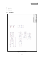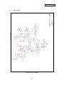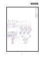
1
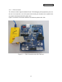
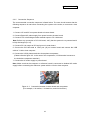
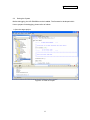
AN706-00042-1v0-E 32-BIT MICROCONTROLLER MB9B100A/MB9B300A/MB9B400A/MB9B500A Series FM3 family inverter reference board User Manual TM ARM and Cortex-M3 are the trademarks of ARM Limited in the EU and other countries. AN706-00042-1v0-E All Rights Reserved. The contents of this document are subject to change without notice. Customers are advised to consult with FUJITSU sales representatives before ordering. The information, such as descriptions of function and application circuit examples, in this document are presented solely for the purpose of reference to show examples of operations and uses of Fujitsu semiconductor device; Fujitsu does not warrant proper operation of the device with respect to use based on such information. When you develop equipment incorporating the device based on such information, you must assume any responsibility arising out of such use of the information. Fujitsu assumes no liability for any damages whatsoever arising out of the use of the information. Any information in this document, including descriptions of function and schematic diagrams, shall not be construed as license of the use or exercise of any intellectual property right, such as patent right or copyright, or any other right of Fujitsu or any third party or does Fujitsu warrant non-infringement of any third-party’s intellectual property right or other right by using such information. Fujitsu assumes no liability for any infringement of the intellectual property rights or other rights of third parties which would result from the use of information contained herein. The products described in this document are designed, developed and manufactured as contemplated for general use, including without limitation, ordinary industrial use, general office use, personal use, and household use, but are not designed, developed and manufactured as contemplated (1) for use accompanying fatal risks or dangers that, unless extremely high safety is secured, could have a serious effect to the public, and could lead directly to death, personal injury, severe physical damage or other loss (i.e., nuclear reaction control in nuclear facility, aircraft flight control, air traffic control, mass transport control, medical life support system, missile launch control in weapon system), or (2) for use requiring extremely high reliability (i.e., submersible repeater and artificial satellite). Please note that Fujitsu will not be liable against you and/or any third party for any claims or damages arising in connection with above-mentioned uses of the products. Any semiconductor devices have an inherent chance of failure. You must protect against injury, damage or loss from such failures by incorporating safety design measures into your facility and equipment such as redundancy, fire protection, and prevention of over-current levels and other abnormal operating conditions. If any products described in this document represent goods or technologies subject to certain restrictions on export under the Foreign Exchange and Foreign Trade Law of Japan, the prior authorization by Japanese government will be required for export of those products from Japan. The company names and brand names herein are the trademarks or registered trademarks of their respective owners. Copyright© 2011 FUJITSU SEMICONDUCTOR LIMITED all rights reserved 1 AN706-00042-1v0-E Revision History Rev Date Remark 1.0 Jul. 13, 2011 First Edition 2 AN706-00042-1v0-E Table of Contents Revision History.................................................................................................................... 2 Table of Contents.................................................................................................................. 3 1 2 3 4 Introduction.................................................................................................................... 6 1.1 Overview ................................................................................................................ 6 1.2 Features ................................................................................................................. 7 Getting Start................................................................................................................... 9 2.1 System Components .............................................................................................. 9 2.2 Connectors of System .......................................................................................... 10 2.2.1 Connectors on Power Board ......................................................................... 10 2.2.2 Connectors on DC-Link Board....................................................................... 12 2.2.3 Connectors on Inverter Board ....................................................................... 13 2.2.4 JTAG connection ........................................................................................... 15 2.2.5 Connection Sequence ................................................................................... 16 2.3 Debug the System ................................................................................................ 17 2.4 FLASH programming using UART........................................................................ 19 Motor Control GUI ....................................................................................................... 20 3.1 Software Overview ............................................................................................... 20 3.2 Setup the USB-to-UART connection .................................................................... 21 Hardware ..................................................................................................................... 22 4.1 Power Supply Board............................................................................................. 22 4.1.1 EMI filter stage .............................................................................................. 22 4.1.2 Power supplies .............................................................................................. 22 4.2 In-Rush Limiter ..................................................................................................... 22 4.3 Active PFC Stage ................................................................................................. 23 4.3.1 Boost chopper ............................................................................................... 23 4.3.2 PFC feedback circuit ..................................................................................... 23 4.3.3 Fault circuit.................................................................................................... 24 4.4 3- Phase Invert Stage ........................................................................................... 24 4.4.1 Power Module ............................................................................................... 24 4.4.2 Feedback Circuit ........................................................................................... 25 4.4.3 Fault Circuitry ................................................................................................ 25 4.5 MFT1 and MFT2 Ports ......................................................................................... 26 4.6 Isolated Ports........................................................................................................ 27 4.6.1 Isolated SPI................................................................................................... 27 3 AN706-00042-1v0-E 4.6.2 4.7 5 Isolated UART ............................................................................................... 27 Serial Programming Port ...................................................................................... 28 Appendix...................................................................................................................... 29 5.1 Schematic............................................................................................................. 29 5.1.1 Power Board ................................................................................................. 29 5.1.2 Inverter Board................................................................................................ 30 5.1.3 DC-Link Board............................................................................................... 34 4 AN706-00042-1v0-E Preface About this manual This book provides the detail hardware information of the Inverter reference Board with Fujitsu’s FM3 family. It describes the features of the reference board and how to get start with it. The hardware circuits of this reference board also are provided. The document is organized as follows: Chapter 1. “Introduction” – This chapter introduces the Inverter Reference Board with Fujitsu’s FM3 family and provides a brief overview of its features. Chapter 2. “Getting Start” – This chapter provides information on getting started with the Inverter Reference Board. Chapter 3. “Motor Control GUI” – This chapter introduces the motor control GUI briefly. Chapter 4. “Hardware” – This chapter describes the hardware on the Inverter Reference Board. Appendix. – This appendix provides schematics, as well as pin arrangement for the Inverter Reference Board. Related document MB9BFxxx Series PERIPHERAL MANUAL Other Users Manual of Inverter Solution 5 AN706-00042-1v0-E 1 Introduction Introduction of the reference board 1.1 Overview The Inverter Reference Board with Fujitsu’s FM3 family is intended to aid the user in the rapid evaluation and development of motor control applications using MB9B500 Series MCU which are embedded with ARM Cotex-M3 CPU core. This reference board is targeted to control Permanent Magnet Synchronous Motors in sensor-less operation. The reference board has a three-phase power module device that contains the motor inverter and the gate driver’s circuit. It also has Power Factor Correction (PFC) circuitry and in order to provide a full set of tools used in motor control applications. If the user doesn’t need PFC stage, a rectifier module is also provided for selection. Figure1-1 is a system block diagram of Inverter Reference Board. The rated continuous output current from the inverter is 10A (RMS). This allow up to 2.2KW output when running from a 220V single-phase input voltage in a maximum 25ºC ambient temperature environment. 6 AN706-00042-1v0-E AC Main Supply PFC Output DC Bus Figure 1-1: 1.2 System Block Diagram Features This reference board is consisted with three parts named as power board, DC-Link board and inverter board. The key features of the reference board are listed as below: Power board: 90V~265VAC input compatible. Four channels of power supply rails: 15V for IPM and PFC module, 5V for MCU system, 5V for isolation chip, 5V for cooling fans. 90V~265VAC output went through line filter. PFC stage of Inverter board: Maximum input voltage 90 V~265 VAC. Adapt PFC module includes rectifier bridge, fast recovering diode, IGBT. VAC input voltage sensing. 7 AN706-00042-1v0-E DC bus sensing. DC Over-voltage protection. Current Feedback circuitry. Over-current protection. Zero-crossing detection. Inverter stage of Inverter board: Three-phase inverter bridge with a power rating of 400V/10A Phase current sense resistor for dual shunt vector control Over-current protection Input / Output of Inverter board: 15V and 5V power supply input (J5). MFT1 port for motor control and PFC signals input or output (J2). MFT2 port for 2nd channel of motor control signal output (J6). Two channels of quadrature encoder interface (J7, J8). Isolated Communication Ports: SPI communication port (J10). UART communication port (J9). Programming and debug interface: JTAG via 20- pin port (J3). Serial programming port: Serial programming port (J1). Additional Protection Circuitry: 250 VAC/15A fuse In-rush current limiter EMI filter 8 AN706-00042-1v0-E 2 Getting Start Getting start with the hardware, firmware and software 2.1 System Components This reference system is made up with three daughter board. They are: Power Board This board contains the EMI filter stage and an AC-to-DC module. The AC-to-DC module can output a stabled 15V (15W) power line. It will be transformed to two 5V power lines through line regulators, one is for MCU system and another is for cooling fans. At the same time, isolated 5V power line comes from the 15V line by isolated DC-to-DC, and another isolated 5V is for isolation communication device. Inverter Board There are PFC stage and Inverter stage, as well as a full bridge rectifier module provided for selection when the user doesn’t need PFC stage. DC-Link Board DC-Link Board can make smoothly 100Hz half-sine-wave power and it can provide to DC bus through three electrolytic capacitors. The input and output cables should be with the minimum current rating of 10A. Figure2-1 shows the connection of the boards. 9 AN706-00042-1v0-E Figure 2-1: Connection of the Boards 2.2 2.2.1 Connectors of System Connectors on Power Board The connectors on power board are shown in Figure2-2. 10 AN706-00042-1v0-E Figure 2- 2 Connectors on Power Board Table 2-1 collects the definition of the connectors on power board. Table 2- 1 Definition of Connectors on Power Board Number Port Designator Description 1 P1 N input of AC mains 2 P2 L input of AC mains 3 P3 Earth Ground 4 P4 L output of filtered AC mains 5 P5 N output of filtered AC mains 6 J1 15V_C,5V_C output 7 J2 5V_A output 8,9 J3,J4 Power supply for cooling fans 11 AN706-00042-1v0-E 2.2.2 Connectors on DC-Link Board The connectors on DC-Link are shown in Figure2-3. Figure 2- 3 Connectors on DC-Link Board Table 2-2 collects the definition of the connectors on DC-Link board. Table 2- 2: Definition of Connectors on DC-Link Board Number Port Designator Description 1 P1 PFC positive input 2 P2 GND 3 P3 DC bus positive output 4 P4 GND 12 AN706-00042-1v0-E 2.2.3 Connectors on Inverter Board The connectors on Inverter board are shown in Figure2-4. Figure 2- 4 Connectors on Inverter Board 13 AN706-00042-1v0-E Table 2-3 collects the definition of the connectors on Inverter board. Table 2- 3: Definition of the Connectors on Inverter board Number Port Designator Description 1 P1 L input (to P4 on power board) 2 P2 N input ( to P5 on power board) 3 P3 PFC positive output (to P1 on DC-Link board) 4 P4 GND( to P2 on DC-Link board) 5 P5 PFC inductor connector 6 P6 PFC inductor connector 7 P7 Motor phase U 8 P8 Motor phase V 9 P9 Motor phase W 10 P10 DC bus positive input(to P3 on DC-Link board) 11 P11 GND(to P4 on DC-Link board) 12 J1 Serial programming port 13 J2 MFT1 port 14 J3 JTAG port 15 J4 5V_A input 16 J5 15V_C,5V_C input 17 J6 MFT2 port 18,19 J7,J8 Quadrature Position/Revolution counter interfaces 20 J9 Isolated SPI port 21 J10 Isolated UART port 14 AN706-00042-1v0-E 2.2.4 JTAG connection The reference board supports standard 20-pin JTAG debugging and programming .By now, the user is recommend to use IAR system tools including the emulator and complier since our project is developed with IAR system tools. Figure 2-4 shows the connection between the reference systems with J-link. Figure 2- 1 JTAG Connection with IAR JTAG tool 15 AN706-00042-1v0-E 2.2.5 Connection Sequence The recommended connection sequence is listed below. The user should ensure that the following sequence is met before connecting the system to the mains, a motor and a host computer. 1. Connect 15V and 5V from power board to inverter board. 2. Connect filtered AC mains supply from power board to inverter board. 3. Connect PFC or half-bridge rectifier module output to DC-Link board. Note: Before any connection to DC-Link board, verify that the system is not powered and it is fully discharged (D1 off). 4. Connect DC-Link output to DC bus input on inverter board. 5. Connect the IDC-20A male to JTAG port (J3) on inverter board and connect the USB cable of J-Link to host computer. 6. Connect the U/V/W phase terminal to three phase compressor. (Please refer the figure 2-5. In the case of the compressor, U/V/W terminal connects to the clockwise compressor terminal.) 7. Connect the AC mains supply to power board. Note: Make sure that the computer or reference board is connected to isolated AC mains supply before connecting the reference system with the J-link or host computer. Figure 2- 2 Connection between inverter board and compressor (For example, U is red line, V is black line, and W is blue line.) 16 AN706-00042-1v0-E 2.3 Debug the System Before debugging, the IAR EWARM must be installed. The firmware is developed with it. How to prepare for debugging, please refer as follows: 1. Open the target project. Figure 2- 6 View of Project 17 AN706-00042-1v0-E 2. Click right button on the project name, and select rebuild all. The project will be rebuilt. Figure 2- 7 Rebuild the Project 3. Select Project->Download and Debug Figure 2- 8 Download and Debug the Project 18 AN706-00042-1v0-E For more information about the firmware project, please refer to the Users Manual of Firmware part. 2.4 FLASH programming using UART The user can program the MCU with UART interface. Please prepare below items: 1. UART -to- RS232 conversion device (The board has the device.) 2. FLASH Serial programming software The port for downloading is J1.It’s definition is as below: Table 2- 4: Pin definition of J1 Pin of Port Net lab Description 1 PRO_RX Data input 2 PRO_TX Data output User can take these steps to programming the flash. 1. Connect the PC and reference board via UART- to- RS232. 2. Connect the jumper JP3 that keeps the MD0 ‘H’. 3. Push SW2 to keep the P60 ‘L level’. 4. Power on the reference board and reset the MCU by pressing the SW1. 5. Programming the flash using FUJITSU FLASH MCU Programmer for FM3. Figure 2-9 shows the interface of software. Figure 2- 9 Fujitsu Flash MCU Programmer for FM3 19 AN706-00042-1v0-E 3 Motor Control GUI This chapter will introduce the GUI 3.1 Software Overview Fujitsu provides a computer-based interface for this reference board. The GUI provides a wide range of control functions for motor operations. Not only can user set the speed and rotation direction, but only can observe the value of constants and variables, or configure the key parameter of the system. This GUI supports Chinese and English language. The user can select one of them at the same time. Figure 3-1 provides the main view of GUI. Figure3- 1 View of GUI 20 AN706-00042-1v0-E 3.2 Setup the USB-to-UART connection The reference board provides an isolated UART port to communicate with a USB-to-UART board. This board is connected to the PC through USB port. In order to ensure the communication, it is recommended shorting the length of wires. The user can connect the communication kit as below: Figure3- 2 USB-to-UART connection For more information of GUI, please refer the GUI user manual. 21 AN706-00042-1v0-E 4 Hardware This chapter describes the hardware circuitry and components of the reference board. 4.1 Power Supply Board This board contains the EMI filter circuit and the AC-to-DC module. It will supply AC mains and low voltage power rails to inverter board. 4.1.1 EMI filter stage This circuit consists of the following components: F1-- 15A/250VAC fast acting fuse ZR1, ZR2 -- Across the incoming AC power supply lines to suppress high energy transients. R1 -- The resistor that is used to discharge the C1 and C4 safely. L1, C2, and C3 -- These three components make up a common noise filter. C2, C3 are Y capacitors. C1, C4 -- Film capacitors to aid in the suppression of EMI. 4.1.2 Power supplies The power board provides the 15-volt power supply using an isolated AC-to-DC power module (U1). The output voltage is regulated at 15-volt with a maximum output current of 1 A, As a result maximum power is 15W. This 15-volt power rail supplies to the PFC and IPM module directly, and three 5-volt power sources are generated. Two of them are created using line regulators (U2, U3) and another one is created using isolated DC-to-DC module (U4). The 5V_C is for MCU system including MCU, JTAG interface, one side of the isolation chips and current feedback circuit of PFC stage etc and 5V_A is for another side of the isolation chips. 4.2 In-Rush Limiter Three high voltage electrolytic capacitors are mounted on the circuit. There will be a huge current rush flows through the circuit when power is supplied. PTC (PTC1) connected in the AC_L line can prevent the current rush. The relay (RL1) connected in panel with PTC is used to short the PTC after a short period when the current get into a normal range. 22 AN706-00042-1v0-E 4.3 Active PFC Stage 4.3.1 Boost chopper The active PFC circuit is a simple boost chopper type. It can control to aim ideal input current to follow the incoming main supply voltage waveform. A special module “FPAB30BH60” has full-bridge rectifier, IGBT, gate driver and fast recovering diode. It is used as core component of the PFC circuit. The input voltage range of the module is 90V~265VAC. The IGBT can tolerant with 600VAC-30A. For more information, please refer to datasheet of “FPAB30BH60”. To make up a boost chopper circuit, the user is required to add an external choke through existing connectors. The recommended specification of choke is 2~4 mH / 15A. 4.3.2 PFC feedback circuit There are four feedback signals. These are required to implement digital PFC function. They are: Rectified input voltage DC bus voltage Rectified input current Rectified input voltage zero-crossing event The rectified input voltage comes from the voltage divider that consists of R12, R13 and R16. The range of voltage is 0~4.0V when AC mains input range is from 90VAC to 265VAC. There is RC filter, made of R14 and C7, between some resisters and ADC pin. D3, diode, can limit to 5V as a maximum voltage. As the rectified input voltage, the DC bus voltage comes from some resisters. It consists of R2, R3 and R8. DC bus voltage passes through the filter that is made of R4 and C2. D1, diode, can limit to 5V as a maximum voltage. Rectified input current is measured using the shunt resistor R17 and the amplifier U4C unit. The gain of amplifier is set at 5. Rectified input voltage zero-crossing event is sensed using a voltage divider (R21, R22) and an opt-coupler (U3). 23 AN706-00042-1v0-E 4.3.3 Fault circuit DC Bus Over-voltage, this fault signal is generated when the maximum voltage limit on the DC bus rails is reached. The threshold value is set to 390 V. The comparison of the threshold value and the amplified DC bus voltage is done by amplifier unit U4C. The threshold limit is set by R31 and R32. DC Bus Over-current, this fault signal is generated when the maximum current limit of 16A is reached. The comparison of the threshold value and the actual current is done by amplifier unit U4B. The threshold limit is set by R27 and R29. 4.4 4.4.1 3- Phase Invert Stage Power Module The three-phase inverter is embedded in a power module (U5). This power module contains: 600V/15A 3-phase IGBT Inverter Bridge built-in bootstrap diode and VS output Short-circuit protection Divided negative dc-link terminals for inverter current sensing applications Gate Driver Power Supply Under-voltage protection Single-grounded power supply Isolation rating of 2000Vrms/min Maximum switching frequency: 20 kHz The MCU provides the PWM signals to this power module in order to turn on/off the IGBT, therefore the power is applied to the motor phases. Two fault conditions will turn off the low side IGBTs: a. Under-voltage of 15V (high side). b. The voltage on CSC pin is higher than 0.5V. At the same time the module will output low level from VFO pin. A pull-up resister is need on VFO pin because it is open-collector type. If you want to know more detail, please refer to the each device’s datasheet. 24 AN706-00042-1v0-E 4.4.2 Feedback Circuit Inverter Leg Shunt Resistor Feedback, a shunt resistor is located between the emitter of the low side switches U, V, W and the “-DC bus”. A simple differential amplifier circuit is used as shown in Appendix A. The operation of the circuit used for the U-phase leg is described below: The current is measured using the shunt resistor R43 and the operational amplifier L224D (U6C); R50, R51, R53, R54 and R55 set the gain. The output of the TL431 (U7) shifts the voltage of the shunt resistor with 2.5V DC offset level. Hence the voltage applied to the ADC of MCU channel varies within 2.5~4.75V. R52 and C27 filter out the high-frequency noise. The same topology is used for the phase V,W. Quadrature Position/Revolution Counter (QPRC) Feedback, this feedback signal provides exact rotor position to the MCU. There are two QPRCs in the MCU. Each counter contains three channels A, B and Z. They are pulled up to the +5V by resisters respectively. J7, J8 are used as the feedback signal input ports. The boards can supply + 5V to the optical-electric encoder which is fixed in the motor through the port. 4.4.3 Fault Circuitry Phase Over- current Protection, an operational amplifier (U6D) acts as a comparator to compare the amplified voltages on shunt resistors with the regulated 2.5V. One channel of voltage is higher than 4.75V DC. The U6D will output a high level up to 13.5V to the power module. This fault signal can turn the low side IGBTs off. The threshold of the phase over-current protection can set 15A as default value. 25 AN706-00042-1v0-E 4.5 MFT1 and MFT2 Ports The MB9B500 Serial MCU is embedded with two Multi-Function Timer (MFT) modules. This reference provides two ports to output or input MFT control and feedback signals. The J2 port contains four parts: motor control, motor feedback, PFC control and PFC feedback. The J6 contains two parts: motor control and feedback. Table 4-1 shows the pin definition of J2. Table 4- 1: Pin Definition of J2 Pin of Port Net lab Description 1 PWM_UP High side signal for U phase 2 PWM_VP High side signal for V phase 3 PWN_WP High side signal for W phase 4 PWM_UN Low side signal for U phase 5 PWM_VN Low side signal for V phase 6 PWN_WN Low side signal for W phase 7 GND_C Digital GND 8 5V_C 5V 9 15V_C 15V 10 VFO_IPM Fault signal from IPM 11 GND_C Digital GND 12 S_U U phase current 13 S_V V phase current 14 S_W W phase current 15 IPM_RTH Temperature of IPM 16 RLY System relay 17 I_AC System current 18 V_DC DC bus voltage 19 V_AC Rectified AC voltage 20 PFC_RTH Temperature of PFC module 21 GND_C Digital GND 22 Zero Check Zero-crossing event detection 23 PRT_DC Over-voltage protection 24 VFO_PFC Fault signal from PFC module 25 PWM_PFC PWM signal to PFC module 26 NULL not connected 26 AN706-00042-1v0-E Table 4-2 shows the pin definition of J6. Table 4- 2: Pin Definition of J6 Pin of Port Net lab Description 1 PWM_UP_EXT High side signal for U phase of extended IPM 2 PWM_VP_EXT High side signal for V phase of extended IPM 3 PWM_WP_EXT High side signal for W phase of extended IPM 4 PWM_UN_EXT Low side signal for U phase of extended IPM 5 PWM_VN_EXT Low side signal for V phase of extended IPM 6 PWM_WN_EXT Low side signal for W phase of extended IPM 7 GND_C Digital GND 8 5V_C 5V_C 9 15V_C 15V_C 10 VFO_IPM_EXT Fault signal from extended IPM 11 NULL not connected 12 S_U_EXT U phase current from extended motor 13 S_V_EXT V phase current from extended motor 14 S_W_EXT W phase current from extended motor 15 IPM_RTH_EXT Temperature of extended IPM 16 NULL not connected 4.6 Isolated Ports These isolated ports are powered by an isolated DC-to-DC. It provides galvanic isolation rated up to1500 VDC/second. 4.6.1 Isolated SPI This interface is based on the trip-channel digital isolator ISO7231A. It has two channels, one is in direction and the other channel is in opposition. The communication speed is up to 1Mbps. 4.6.2 Isolated UART This interface is based on the ISO7221B which provides two isolation channels. The channels are oriented in opposite directions. The communication speed is up to 5Mbps. 27 AN706-00042-1v0-E 4.7 Serial Programming Port Except the JTAG port, the user can program the MCU by serial programming port-J1. This port is connected to the UART0 with the RX pin connected the +5V by a resister R79. The SW2 is used to shift the level on P60, as well as JMP3 is used to shift the level on MD0. When P60 = 0 and MD0 = 1, the programming is allowed, or it is disabled. 28 AN706-00042-1v0-E 5 Appendix 5.1 5.1.1 Schematic Power Board Figure 6- 1 Power Board 29 AN706-00042-1v0-E 5.1.2 Inverter Board Figure 6- 2 PFC stage 30 AN706-00042-1v0-E Figure 6- 3 Inverter Stage 31 AN706-00042-1v0-E Figure 6- 4 MCU system 32 AN706-00042-1v0-E Figure 6- 5 Connectors 33 AN706-00042-1v0-E 5.1.3 DC-Link Board Figure 6- 6 DC-Link Board - End - 34