1
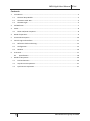
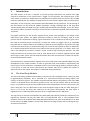
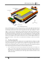
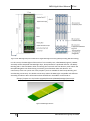
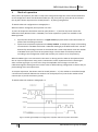
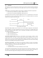
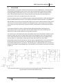
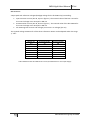
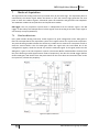
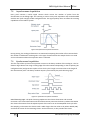
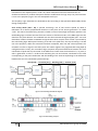
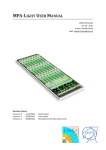
MPA-LIGHT USER MANUAL Davide Ceresa*, Jan Kaplon, Kostas Kloukinas and Alessandro Marchioro. CERN PH-ESE-ME , 16-03-2015, *corresponding author: [email protected] Revision History Version 1.0 Version 1.1 11/11/2014 16/03/2015 Draft version First version MPA-Light User Manual V1.1 Contents 1 Introduction .................................................................................................................................... 3 1.1 The Pixel Strip Module ............................................................................................................ 3 1.2 The Macro Pixel ASIC .............................................................................................................. 4 1.3 The MPA-Light......................................................................................................................... 5 2 Pad Definition ................................................................................................................................. 7 3 Power .............................................................................................................................................. 8 3.1 Power On/Down sequence ..................................................................................................... 8 4 Mode of operation .......................................................................................................................... 9 5 Functional Description .................................................................................................................. 10 5 Control Logic and Interface ........................................................................................................... 11 6 5.1 Reference Clocks and timing ................................................................................................. 12 5.2 Configuration ........................................................................................................................ 13 5.3 Readout ................................................................................................................................. 16 Front-End ...................................................................................................................................... 17 6.1 7 Specifications .................................................................................................................... 18 Modes of Acquisition .................................................................................................................... 20 7.1 Pixel architecture .................................................................................................................. 20 7.2 Asynchronous Acquisition..................................................................................................... 21 7.3 Synchronous Acquisition ....................................................................................................... 21 2 Microelectronics group at CERN MPA-Light User Manual V1.1 1 Introduction The CMS tracker at HL-LHC is required to provide prompt information on particles with high transverse momentum to the central Level 1 trigger. For this purpose, the innermost part of the outer tracker is based on a combination of a pixelated sensor with a short strip sensor, the so-called Pixel-Strip module (PS). The readout of these sensors is carried out by distinct ASICs, the Strip Sensor ASIC (SSA), for the strip layer, and the Macro Pixel ASIC (MPA) for the pixel layer. The processing of the data directly on the front-end module represents a design challenge due to the large data volume (30720 pixels and 1920 strips per module) and the limited power budget. This is the reason why several studies have been carried out to find the best compromise between ASICs performance and power. The higher luminosity for the Phase-II upgrade of LHC entails new challenges in the design of the CMS silicon outer tracker. The higher granularity needed to keep the occupancy level at a few percent and the requirement of having a good estimation of the z-coordinate of the hit gives rise to the need of pixelated sensors. Furthermore, to keep the Level1 (L1) trigger rate at an acceptable level (500 kHz to 1 MHz) requires the capability to perform quick recognition of particles with high transverse momentum (pT). A particle traversing a set of two sensors spaced by about 2 millimetres at an almost perpendicular direction to the plane of the sensors generates a, so called, "stub". The stub is the elementary primitive to build a vector of these high momentum particles. The stub finding is based on the concept that a low pT track bends more in the 3.8T magnetic field of CMS than a high pT track, and it uses the distance between hits from the same track in these two sensors to discriminate between them. The requirements mentioned above together with the limited power and material budget drive the development of the tracker modules: in order to generate stubs each module is composed by two sensor layers, the first of which is a pixelated sensor to ensure the high granularity, while the other is a strip sensor to limit the power consumed by the readout ASICs and to reduce the number of electrical lines on the hybrid. This module is called Pixel-Strip (PS) Module. 1.1 The Pixel Strip Module This new stub finding module accommodates a strip sensor and a pixelated sensor, covering an area of approximately 5cmx10cm, and is mounted on a mechanical assembly providing support and cooling, as shown in figure 1. This module can be placed with different orientations in the outer CMS tracker: in the barrel layers, the beam is parallel to the z-axis of the module, while in the end cap layers, it is parallel to the y-axis of the module and in both configurations the x-axis stays on the r-phi plane. Along the x-axis, the dimensions of the strips and pixels length is 100 um, while along the zaxis it is 2.5 cm for the strips and 1.446 mm for the pixels. Consequently, the strip sensor is segmented into 2 x 960 strips while the pixel sensor is segmented into 32 x 960 pixels. The strip sensor is read out from 16 Short Strip ASICs (SSA). Wire bonds provide the connectivity to a high-density substrate carrying the ASICs that are bump-bonded onto it. The pixelated sensor instead is read out by 16 Macro Pixel ASICs (MPA) distributed in two rows bump-bonded on it. Wire bonds connect the MPA periphery to the same substrate carrying the SSA, hence realizing the topto-bottom connectivity. 3 Microelectronics group at CERN MPA-Light User Manual V1.1 Figure 1 PS Module Exploded view From a functional point of view, the SSA processes the sensor strip signals and sends the hit information to the MPA at each bunch crossing. The latter stores the full event (pixel and strip hits) and correlates the hits from the two sensors to generate the stubs. Upon reception of a Level 1 trigger, i.e. after the Level 1 trigger latency, the MPA sends the whole event information to the readout back-end electronics. The generated stubs are instead sent out at each bunch crossing to the trigger back-end electronics with latency, due to the stub finding process. The MPA output data does not reach directly the CMS back-end: another ASIC, the Concentrator IC (CIC), aggregates the data from the 16 MPAs on each module and sends them to the Low Power GigaBit Transceiver (LPGBT) which transmits a serial stream to the CMS back-end through an optical link transceiver (VTRx+). 1.2 The Macro Pixel ASIC The large size of the pixelated sensor requires the use of 16 MPA ASICs for reading out a single sensor. Every chip connects to 120 x 16 pixels and it is composed by a pixel matrix region of 12mm x 23.16mm and a periphery region of about 2 mm that resides on one edge of the chip as shown in figure 2 (top). The MPA logic processes at each bunch crossing the data from the pixel front-end and from the SSA through three functional blocks as illustrated in figure 2 (bottom): • The L1 data block stores the full event information and sends them out if receives a L1 trigger. It stores the hit information from the two front-ends (Pixel and Strip) without any data reduction in the L1 Memories for the duration of the L1 latency. Upon arrival of a L1 trigger, the event is processed by the L1 Data Logic which encodes the position of each cluster and its width. 4 Microelectronics group at CERN MPA-Light User Manual V1.1 Figure 2 Top: MPA structure with dimensions. Bottom: PS module block diagram with detailed MPA • • 1.3 The stub finding logic receives the same input of the L1 data block synchronously with the 40 MHz bunch crossing frequency and looks for coincidences within a narrow geometrical angle between pixel and strip clusters in order to find and encode the stubs. The Output Interface organizes data from the two previous blocks and transmits them to the Concentrator IC at a frequency of 320 Mbit/s. More details about Data format and Simulation studies at: https://espace.cern.ch/Tracker-Upgrade/Electronics/CIC/default.aspx The MPA-Light The MPA-Light is the first prototype of the Macro Pixel ASIC in a 65 nm Low Power CMOS technology. It consists in a reduced size MPA with a pixel array of 16 x 3 pixels, instead of 120 x 16 pixels. It integrates bump-bond pads for sensor connections and wire bond pads for hybrid connections. The size of the single pixel will be 100 x 1446 µm like the final MPA. The principal purposes of this ASIC are to prototype and qualify the analog Front-End circuitry, to facilitate the development of the sensor and to understand and solve the technical aspects of the module assembly. MPA MPA-Light Pixel/Row 120 16 Row/Chip 16 3 Width 12 mm 1.7 mm Length 25.16 mm 6.338 mm Pixel Width 100 um 100 um Pixel Length 1446 um 1446 um Figure 3 MPA structure with connectivity 5 Microelectronics group at CERN MPA-Light User Manual V1.1 Figure 4 Left: MPA-Light floorplan and dimensions. Right: MPA-Light connectivity (BB Bunp bonding, WB Wire bonding) For this reason, the MPA-light will be used in a first assembly-test, called MaPSA (Figure 5). MaPSA assembly will be composed of 6 MPA-light chips, bump-bonded to a pixelated detector. The BumpBonding pads in the Pixel Matrix allow connecting the Front-End with the detector pixels. While The Bump-Bonding Bias Line allows having a common ground between ASIC and detector. The connectivity to the test system sits in the periphery and it is available for both bump bonding and wire bonding connectivity. The double connectivity makes the MPA-Light compatible with different assembly procedures. More information about the different assemblies can be found at: https://espace.cern.ch/Tracker-Upgrade/Electronics/MaPSA/SitePages/Home.aspx . Figure 5 MaPSA-Light 3D view 6 Microelectronics group at CERN MPA-Light User Manual V1.1 2 # 1 2 3 4 5 6 7 8 9 10 11 12 13 14 15 16 17 18 19 20 21 22 23 24 25 26 27 28 29 30 31 32 Pad Definition Name CLK+ OUTRO CLKOUTCONF HITOR SHUTTER CALSTROBE OUTMEM STROBE EMPTY STRIP1 CLKRO STRIP2 DATARO STRIP3 DATACONF STRIP4 ENCONF CLKCONF DVSS DVDD PVDD VSSPST VDDPST AVDD AVSS AVDD AVSS VBIAS VBIFEED VBIPRE CAL Type CML Input Digital Output CML Input Digital Output Digital Output Digital Input Digital Input Digital Output Digital I/O Digital Output Digital I/O Digital Input Digital I/O Digital Input Digital I/O Digital Input Digital I/O Digital Input Digital Input Ground Power Power Ground Power Power Ground Power Ground Voltage Ref Voltage Ref Voltage Ref Analog Output Value 0.6/1.2 V 0/2.5 V 0.6/1.2 V 0/2.5 V 0/2.5 V 0/2.5 V 0/2.5 V 0/2.5 V 0/2.5 V 0/2.5 V 0/2.5 V 0/2.5 V 0/2.5 V 0/2.5 V 0/2.5 V 0/2.5 V 0/2.5 V 0/2.5 V 0/2.5 V 0V 1.2V 1.2V 0V 2.5V 1.2 V 0V 1.2 V 0V 0.3V 0.3V 0.3V Description High Input Differential Clock. (CML) SPI Readout Data Output Low Input Differential Clock (CML) SPI Configuration Data Output OR Trigger Output Acquisition/Readout Enable On-chip test capacitance strobe Periphery Memory Data Output Strip Data transmission strobe Output signal for periphery memory status Strip Data transmission line SPI Readout Clock Strip Data transmission line SPI Readout Data Input Strip Data transmission line SPI Configuration Data Input Strip Data transmission line SPI Configuration Enable SPI Configuration Clock Digital Ground Digital Power Supply Periphery Logic Power Supply I/O Ground I/O Power Supply Analog Power Supply Analog Ground Analog Power Supply Analog Ground Reference for Analog Purpose Reference for Analog Purpose Reference for Analog Purpose Calibration DAC Probe point Figure 6 Pad Numbering and Pad dimensions in um 7 Microelectronics group at CERN MPA-Light User Manual V1.1 3 Power • • • • 3.1 DVDD - Digital Supply: 1.2 V supplies the Digital Logic in the entire chip but the Periphery Logic. Corresponding ground is DVSS. PVDD - Periphery Supply: 1.2 V supplies the Periphery Logic. Ground is common with DVDD (DVSS). AVDD – Analog Supply: 1.2 V supplies Bias Structure and Analog Front-End. Corresponding Ground is AVSS. VDDPST I/O Supply: 2.5 V supplies the I/O Pad. Corresponding ground is VSSPST. Power On/Down sequence Digital I/O pads contain a Power On Control (POC) system to prevent I/O unknown state. For this reason a particular Power On sequence must be followed: 1. 2. 3. 4. Turn On the VDDPST voltage (2.5V). Turn On the DVDD voltage (1.2V). Turn On the AVDD voltage (1.2V). Turn On the PVDD voltage (1.2V). This voltage is needed only when the synchronous readout is used. For the same reason a particular Power Down sequence must be followed: 1. 2. 3. 4. Turn Off the PVDD voltage. Turn Off the AVDD voltage. Turn Off the DVDD voltage. Turn Off the VDDPST voltage. Rise time of every supply must be > 50 us. 8 Microelectronics group at CERN MPA-Light User Manual V1.1 4 Mode of operation After power-up sequence, the ASIC is ready to be configured through the serial interface dedicated to the configuration which has dedicated enable (Pin 18), clock (Pin 19), input (Pin 16) and output (Pin 4) pads. Shutter input must be closed (Shutter = ‘0’) during configuration. Details about the configuration in Paragraph 5.2. When the ASIC is configured, the acquisition can start: To start the acquisition the Shutter must be open (Shutter = ‘1’) and the chip must receive the differential clock (Nominal value = 160 MHz). Two main acquisition systems are available in the MPA-Light ASIC: • • Asynchronous acquisition consists in a ripple counter per pixel which counts the number of pulses from the Analog Front-End. Synchronous acquisition implements the binary readout. It samples the output of the Analog Front-End with a 40 MHz clock which is obtained dividing by 4 the differential clock. The hits detected by the Analog Front-End are associated with a time stamp which count the number of 40 MHz clock cycles from the acquisition begin. The hits data can also be processed according to the configuration of the ASIC and they are saved in an on-chip memory. When the MPA-Light is not connected to the sensor or during tests the ASIC can be operated with the on-chip test capacitance. Every pixel is connected to a 20 fF capacitance which is discharged when a strobe signal (pin 7) is sent to the chip, the amplitude of the charge is set with the Calibration Digital to Analog Converter whose value is defined during configuration as well as the per pixel enabling of the test capacitance. To stop the acquisition, the Shutter must be closed (Shutter = ‘1’). The readout is controlled through a second serial interface dedicated to readout. The clock pad (Pin 12) controls the readout of the counters (Pin 2) and of the memory (Pin 8). Details about the readout in Paragraph 5.3 Figure 7 Control signal example for configuration, acquisition with two test pulses and readout 9 Microelectronics group at CERN MPA-Light User Manual V1.1 5 Functional Description The MPA-Light design has a Pixel Matrix and a Periphery. Both of them are configured with the Serial Interface for the Configuration and readout with the Serial Interface for Readout. The Pixel Matrix includes 48 pixels distributed in 3 rows. Each pixel is composed of analog Front End (FE) and pixel logic. The Pixel Logic is common for a 2-pixels group and transmits the data to the periphery. The Periphery includes three macro blocks: • The Control Logic is the Logic responsible for the control of the ASIC. It generates the internal shutter, the clear signal and the Sample clock when the Shutter is open. These signals are distributed to the pixel matrix with one column per 8-pixels group and also to the periphery logic. The control logic receives the output signals from the FE and generates a trigger signal (OR-trigger). Also the SPI buses are controlled by the Control Logic You can find details about the control logic in Chapter 5. • The Periphery Logic receives the signals from the Pixel Logics, processes them according to the configuration and saves the results in the memory or sends them out through the Strip I/O. It has a dedicate power supply (PVDD). You can find details about the control logic in Chapter 7. • The Analog Bias generates the current and voltage references for the FE from the three voltage references in input and distributes the Calibration strobe to the Pixel Matrix. You can find details about Analog Bias in Paragraph 6.2 Figure 8 Functional Block Diagram (to review) 10 Microelectronics group at CERN MPA-Light User Manual V1.1 5 Control Logic and Interface The chip is controlled through a limited number of signals: Configuration Serial Interface. The pixel and periphery configurations and the bias setting are handled over a serial interface which consists in a shift register controlled by: • • • • ClkConf is the clock signal for the configuration registers. Data are shifted on the rising edge. DataConf is the input data for the configuration shift register. His value is saved in the first register at each clock cycle. EnConf is the active high enable signal. When low, the chip does not accept input and clock. OutConf is the output of the configuration shift register. It is connected to the output of the last register. Readout Serial Interface. The pixel hit counters and the periphery memory are readout over a second Serial Interface which includes separate data output for counters and memory. The counters are chained in a shift register controlled by: • • • • ClkRO is the clock signal for the counter registers. Data are shifted on the falling edge. DataRO is the input data for the counter registers. His value is saved in the first register at each clock cycle. Shutter is the active low enable signal. When high, the chip does not accept input and clock. OutRO is the output of the counter shift register. It is connected to the output of the last register. The memory is controlled by the same clock and use the same enable, but has dedicated output: • MemOut is the output pin of the memory. This is a separate memory, not on the counter shift register. Shutter signal. The Shutter signal allows to readout the chip when it is low, while when it is high it activates the data acquisition from the analog Front-End. When the Acquisition phase begins, the Control Logic generates three internal signals which are distributed to the Pixel Matrix through a column every 8 pixels and to the Periphery Logic: • • • Clear: Pulse of 1.5 ns (nominal value) which resets all the counter registers and the memory. IntShutter: delayed shutter which starts the acquisition after the clear signal SampleClk: Clock signal for the sampling of the Analog signal from the FE and for the Periphery Logic operation. 11 Microelectronics group at CERN MPA-Light User Manual V1.1 5.1 Reference Clocks and timing System Clock. The MPA-Light system clock has a nominal frequency of 160 MHZ and it has to be provided from the test system . The clock receiver is a CML differential receiver (Pad 1 and 3) with the following specifications: Common Mode 900 mV Nominal levels 600 mV/1.2V Peak-to-Peak Voltage from 200 mV to 600mV Termination resistance 100 Ohm Sample Clock. The SampleClk signal is internally generated with a clock divider. When Shutter is high, the System Clk is divided by 4, obtaining the SampleClk signal (nominal frequency 40MHz). The latter is distributed to the pixel matrix as sampling clock for the binary readout and as clock for the data processing. Sample Clock Phase alignment. The system Clock division by 4 generates a Sample clock with 4 possible phases. The Shutter signal set the phase of the Sample clock: the Sample Clock will be aligned with the first system clock rising edge after the opening of the shutter as shown in figure 9. Consequently, it is good practice to open/close the shutter on the falling edge of the system clock in order to avoid race conditions. Figure 9 Clock divider phase alignment example 12 Microelectronics group at CERN MPA-Light User Manual V1.1 5.2 Configuration Data is loaded into the device through DataConf port and under the control of a serial clock input, ClkConf. In particular, the data is shifted in on the rising edge of ClkConf. The configuration inputs are enabled by the EnConf. The configuration data is divided in two parts: Pixel Matrix and Periphery. Configuration Order Configuration Data are loaded in the following order: 1. Pixel Matrix Configuration: The basic design unit is the 2-pixel group where each pixel contains 10-bit for configuration (8 bits for single pixel and 2 bits for 2-pixel group). Each 2Pixel group word is loaded from the MSB (from bit 19 to 0) and the pixel order is: a. Row 3: From Pixel 48-47 to Pixel 34-33. b. Row 2: From Pixel 17-18 to 31-32. c. Row 1: From Pixel 16-15 to Pixel 2-1. 2. Periphery Configuration: From MSB (from bit 31 to bit 0). Configuration In [511:0] = Pixel 48-47 [511:492] | … | Pixel 2-1[51:32] | Periphery [31:0] The Row2 pixel configuration order is the opposite of Row1 and Row3. Pixel Matrix Configuration Pixel Matrix configuration is loaded as a 20-bit word in the pixel matrix where every word includes: ROW 1 and 3 Bit Number 0 1 2-6 7 8-9 10 11 12-16 17 18 19 13 Bit Name PML ARL TRIMDACL[0:4] CEL CW[0:1] PMR ARR TRIMDACR[0:4] CER SP SR Description Left Pixel Mask Asynchronous Readout Left Pixel Enable 5-bit Trimming DAC Left Pixel Calibration Enable Left Pixel Pixel Clustering Width Right Pixel Mask Asynchronous Readout Right Pixel Enable 5-bit Trimming DAC Right Pixel Calibration Enable Right Pixel Signal Polarity Synchronous Readout Enable Microelectronics group at CERN MPA-Light User Manual V1.1 ROW 2 Bit Number 0 1 2-6 7 8 9 10 11 12-16 17 18-19 Bit Name PMR ARR TRIMDACR[0:4] CER SP SR PML ARL TRIMDACL[0:4] CEL CW[0:1] Description Left Pixel Mask Asynchronous Readout Left Pixel Enable 5-bit Trimming DAC Left Pixel Calibration Enable Left Pixel Signal Polarity Synchronous Readout Enable Right Pixel Mask Asynchronous Readout Right Pixel Enable 5-bit Trimming DAC Right Pixel Calibration Enable Right Pixel Pixel Clustering Width The common configuration bits in the 2-pixel group are Polarity, Cluster width and Pixel Clustering Enable, while the pixel mask, ripple counter enable, TrimDAC and calibration enable are per pixel. You can find detailed information about TrimDAC in Chapter 5. Pixel Mask (PM*) *Left or Right 0 1 Description Front End Output is NOT enabled Front End Output is Enabled Asynchronous Readout (AR*) *Left or Right 0 1 Description Asynchronous Readout is NOT enabled Asynchronous Readout is Enabled Calibration Enable (CE*) *Left or Right 0 1 Description Calibration is NOT enabled Calibration is Enabled Cluster Width (CW) *Left or Right 00 01 10 11 Description Clustering is NOT enabled Clustering Width = 3 Clustering Width = 4 Clustering Width = 5 Signal Polarity (SP*) *Left or Right 0 1 Description Positive Polarity Negative Polarity Synchronous Readout (SR) 0 1 Description Synchronous Readout is NOT enabled Synchronous Readout is Enabled 14 Microelectronics group at CERN MPA-Light User Manual V1.1 You can find detailed information about Pixel Mask, Asynchronous Readout, Cluster width, Signal Polarity and Synchronous Readout in Chapter 7. Periphery Configuration Configuration data is loaded as a 32-bit word in the Periphery (MSB first, from bits 31 to 0): Bit Number 0-1 2-3 4-7 8-11 12-15 16-23 24-31 Bit Name OM[0:1] RT[0:1] SCW[0:3] SH2[0:3] SH1[0:3] CALDAC[0:7] THDAC[0:7] Description Operation Mode Retiming Strip Cluster Width Correlation Offset last 8 columns Correlation Offset first 8 columns 8-bits Calibration DAC 8-bits Threshold DAC The first 16 bit configures the Periphery Logic while the last 16 bits contains the values of the 8-bit DAC used for comparator threshold and calibration pulse. You can find detailed information about Threshold and Calibration DAC in Chapter 6. Operation Mode (OM) 00 01 10 11 Description Stub Finding Logic Mode Strip Emulator Mode Centroid Mode No Processing Mode Retiming (RT) 00 01 10 11 Description No Retiming Pixel Path + 1 clock cycle Strip Path + 1 clock cycle Pixel Path + 2 clock cycle Strip Cluster Width SCW [0:3] represents the Strip Cluster cut between 0 and 8 in binary coding Correlation Offset SH* [0:3] represents the value of the offsets with half pixel precision and with two’s complement coding (offset can be negative). *Left or Right You can find detailed information about Operation Mode, Retiming, Strip Cluster Width and Correlation Offset in Chapter 7. 15 Microelectronics group at CERN MPA-Light User Manual V1.1 5.3 Readout When Shutter is low, the collected data is readout from the device through the OutRO and MemOut pins, under the control of a readout serial clock, ClkRO. Data are sent out on the negative edge of ClkRO. ClkRO control. To avoid timing problems during readout, the ClkRO must fulfill two requirements: • When Shutter opens (Shutter rising edge), ClkRO must be at 0. • When Shutter closes (Shutter falling edge), ClkRO must be at 1. Consequently, when the shutter is high the ClkRO must be set at 1. It is good practice to insert some delay between the shutter opening and the ClkRO setting to 1 to compensate different trace delay between the two signals on the test system. Figure 10 ClkRO control example Asynchronous data readout. The hit counters are in a shift register configuration with dedicated output, OutRO(pin 2), and input, DataRO (pin 14). Data are transmitted on the negative edge of the clock and the ouput pin when shutter is low is connected to the MSB of the 48th pixel counter. The readout pixel order is: 1. Row 3: From Pixel 48 to Pixel 33. 2. Row 2: From Pixel 17 to 32. 3. Row 1: From Pixel 16 to Pixel 1. Asynchronous Readout Header. After the 1st pixel counter, the shift register contains a 32-bit programmable header. The header is loaded during readout through the DataRO pin and is the only register which is not reset at acquisition begin (Shutter opening). This header is useful to check the coherence of the data when they are readout after the acquisition and can be easily loaded sending always one at the DataRO pin during readout for example. Synchronous data Readout. The data from the synchronous readout are saved in the periphery memory composed by 96 words of 72 bits. The ClKRO controls the serial readout of the memory through the MemOut pin. The bit and word readout order are: • From Bit 71 to Bit 0. • From Word 1 (First event saved) to Word 96 (Last event saved) The data format changes depending on the chosen operative mode (see detail in paragraph 7.2) and the memory is not overwritten if the acquisition exceeds the size of the memory. The memory is reset when acquisition begin (Shutter opening) and only the events with data are saved. 16 Microelectronics group at CERN MPA-Light User Manual V1.1 6 Front-End The preamplifier is built with a buffered cascode (input transistor NMOS 9.6 um / 140 nm) loaded with a degenerated PMOS cascode current source and enclosed with Krummenacher feedback providing leakage compensation for the n--on-p+ silicon sensors up to 200nA. An extra current source directly supplying the input transistor provides extra boosting of the bandwidth and minimization of the noise contribution from the active loads. The second stage working as an amplifier/integrator and threshold interface is built with differential folded cascode loaded with resistors. The common threshold for the discriminator is provided by high impedance current source mirroring the output current from an 8-bit mutual DAC and sourcing it to one of load resistors which produces a DC voltage imbalance. The local per-pixel 5-bit DAC is connected to the second load resistor which provides the equalization of the discriminators offset spread. A two stage comparator consists of folded cascode differential amplifier with swing limiter preventing saturation of this stage due to DC threshold voltage at the input, followed by the differential to single ended stage which also provides hysteresis. The overall current consumed by the front end is below 30 uA for the nominal bias condition (input transistor biased with 16 uA). The pulse gain of the front end amplifier seen at the discriminator input is about 95mV/fC (post-extraction simulation) and the peaking time of the amplified pulse from the detector is around 24ns, which limits the time walk of the front end channel (preamplifier/shaper/discriminator) below 14ns for signals ranging between 0.75 and 12fC and the discriminator set to 0.5fC threshold. The simulated noise for the expected input capacitance of around 500fF (280fF detector capacitance + 55fF bonding pad + 160fF ESD) and worst case detector leakage current (50nA) is around 200e- ENC. The schematic of one channel of the front end is shown in figure 11 Figure 11 Schematic diagram of the front end channel comprising preamplifier, differential amplifier/integrator, twostage discriminator and threshold and calibration circuits. 17 Microelectronics group at CERN MPA-Light User Manual V1.1 6.1 Specifications Preamplifier-Shaper characteristics • • • • • • • • Type of the detector: n-on-p+ (DC coupled, maximum leakage 200nA) Gain at discriminator input: ~95 mV/fC (post-extracted simulation, amplitude of analog signal of discriminator) Extracted gain (from S curves): ~85 mV/fC (post-extracted simulation, gain extracted from threshold scans; difference of the analog gain and the extracted gain caused by the minimum overdrive of the comparator and comparator hysteresis) Linearity: INL < 2% in the 0-3 fC range and threshold set to 0.5 fC Peaking Time: 24 ns Time Walk: <14 ns for signals ranging between 0.75-12 fC with threshold set at 0.5 fC PSRR (Worst Case): >10dB Noise (Worst Case): <200e- Comparator Stage A threshold is applied as a differential voltage offset to the comparator stage. This threshold voltage is applied from an internal 8-bit DAC (bits THDAC< 0 : 7 >). • • • Threshold range 0 mV to 370 mV, Nominal setting: 48 mV (DAC = 33 equivalent to 0.5fC) Threshold step 1.456 mV Discriminator offset spread < 90 mV peak-to-peak before trimming The discriminator offset inside each pixel is controllable with 5-bit (bits TRIMDAC<0:4>). • • TrimDAC Threshold range TrimDAC Resolution range 120mV (nominal) 5 bit; step 3.75 mV (nominal) Calibration Circuit Calibration signal, distributed with one calibration line, can be applied to on-chip calibration capacitor (20fF) connected to front end input with CMOS switch controlled with one of the channel configuration bit. Address and the number of connected channels to the calibration line, as well as the amplitude of the calibration signal is set via the control logic. The voltage applied to the Calibration Capacitors by the chopper is determined by an internal 8-bit DAC. The calibration line is also brought to pad (pin 32) where the calibration voltage can be directly measured. • • Calibration signal range Calibration signal step 0-450 mV (charge range 0-9 fC) 1.768 mV (charge 0.035 fC) Calibration DAC is controlled through bits CALDAC< 0:7> of the control registers. 18 Microelectronics group at CERN MPA-Light User Manual V1.1 Bias Structure 3 input pads with reference voltages (bandgap voltage for the final MPA chip) controlling: • • • Input transistor current (Pin 29, Iinput in figure 7). The nominal value of the bias is 16 uA for the control voltage at Pin 29 equal to 300 mV. Krummenacher current (Pin 30, Ikrum in figure 7 ). The nominal value of the bias is 80nA for the control voltage at Pin 30 equal to 300 mV. All remaining bias currents and voltages (14 currents + 4 voltages) (Pin 31) The nominal voltage is 300 mV for all the three references. Biases can be adjusted within the range +/- 25%. Charge (fC) 0.5 1 1.5 2 2.5 3 3.5 4 Threshold (DAC) 33 61 92 121 153 183 212 238 Threshold (mV) 48 89 134 176 223 266 309 347 Table 1 Simulated values for middle of the S curves (Threshold scans for varius input charges) 19 Microelectronics group at CERN MPA-Light User Manual V1.1 7 Modes of Acquisition The signal from the Analog Front-End is processed firstly by the Pixel Logic. The acquisition phase is controlled by the Shutter signal. When the Shutter is open the Control Logic generates the clear pulse to clean the readout register, afterwards opens the IntShutter and generates the SampleClk. The IntShutter enables the Asynchronous and Synchronous modes. OR Trigger. The only acquisition system which is independent from the Shutter signal is the OR trigger. It does always the OR operation of all the signals from the analog FE and the output signal is sent directly as output (HitOR Pin). 7.1 Pixel architecture Every pixel includes Analog Front-End, 10-bits registers for pixel configuration and 2 AND gates to filter the FE output before the acquisition system and a ripple counter for asynchronous acquisition. The pixel clustering module includes also the binary readout and is common for two pixels as well as with the vertical buffers. The first AND gate filters the signal with the Pixel Mask bit of the configuration register, while the second one with the IntShutter signal. If the signal passes the two AND gates, it gets to the two acquisition systems. The Vertical Buffer module buffers the data from the pixel clustering module (Synchronous mode of acquisition), the data for the OR-Trigger (before Shutter AND gate) and the bus from the pixels data from the rows above and transmits them to the next pixel row, towards the periphery. Figure 12 2-pixels architecture 20 Microelectronics group at CERN MPA-Light User Manual V1.1 7.2 Asynchronous Acquisition Every pixel contains a 16-bit ripple counter which counts the number of pulses from the discriminator on the falling edge. The counting is reset at every new acquisition and can be disabled with the AR* (Left or Right) enable configuration bit. The signal polarity does not affect the counting capabilities of the readout system. Figure 13: Asynchronous acquisition waveforms During testing, the analog performances are measured comparing the number of hits counted with the number of calibration strobe signals. In this type of measurement the Sample clock is not used and no information about the acquisition time is collected. 7.3 Synchronous Acquisition The first step of the synchronous acquisition consists in the binary readout of the analog FE. The hit detector logic detects the rising or falling edge of the discriminator depending on the set polarity (SP configuration bit) and generates a pulse of one clock cycle’s length no matter what is the length of the discriminator pulse. The binary readout output is processed by the pixel clustering Logic. Figure 14: Synchronous acquisition waveforms Pixel Clustering Logic. The pixel clustering implements the cluster elimination and centroid extraction. The cluster elimination and centroid extraction processes the binary readout data within the cluster information from the adjacent pixels of the same row in the SampleClk clock cycle after the sampling. It eliminates the clusters with a width larger than the value set by Cluster Width (CW) and finds the center of the remaining cluster. At the same time, it also provides the cluster 21 Microelectronics group at CERN MPA-Light User Manual V1.1 information to the adjacent pixels. If CW = 00, cluster elimination and centroid extraction are disabled and the binary readout data passes without modification this logic step. The processed data is sent to the periphery logic in the next SampleClk clock cycle. The Periphery Logic elaborates the Pixel Matrix data according to the Operation Mode (OM) chosen during configuration: Stub Finding Mode (OM = 00). A particle traversing a set of two sensors spaced by about 2 millimeters at an almost perpendicular direction to the plane of the sensors generates a so called "stub". The stub is the elementary primitive to build a vector of these high momentum particles. The Stub finding logic correlates the data from two sensors to find these stubs. In the MPA-Light case the data from the pixel detector are combined with the data received through Strip[0:3] pins. A 4 to 16 deserializer collects the data at 160 MHz and generate a 16 bit strip hit vector which is processed by the stub finding logic. While pixel clustering is carried out at pixel level, the strip clustering is carried out in the periphery. When the centroids have been computed, their row and column positions are encoded. In order to align the two data path, the retime registers are programmable using RT[0:1] configuration bits. Finally, the coincidence logic computes the position difference between the rows coordinates of pixel and strip centroids: if the difference is lower than the threshold of +/- 4 pixels, a stub is generated. A stub is a 13-bit word containing the row and column coordinates of the stub corresponding to the pixel coordinates and the bending of the stub corresponding to the difference between the two row coordinates (pixel and strip): Stub [0:12] = Z Position [0:1] | Bending [2:6] | Position [7:12] Figure 15 Stub Finding Mode block diagram Figure 16 Stub finding example 22 Microelectronics group at CERN MPA-Light User Manual V1.1 The generated stubs are written in the periphery memory, up to a limit of 4 stubs per bunch crossing and with a Bunch crossing ID of 16-bit (total 72-bit word): Data [0:71] = Stub1[0:12] | Stub2[13:25] | Stub3[26:38] | Stub4[39:51] | BX[52:67] | ‘1111’ The memory stores up to 96 words per acquisition phase and when it is full it does not overwrite. A header of 4-bit at ‘1’ is attached to each word. The Empty signal indicates when the first word is written in the memory. The MPA-Light contains also two modes of operation which activate only some steps of the data processing: No Processing Mode (OM = 11). In the No Processing mode, the periphery logic writes directly in the memory the output of the pixel matrix if there is at least one bit different from 0 with. Every word contains the Pixel Matrix hits, the Bunch crossing ID and an header of 8 bit at 1: Data [0:71] = Pixel Matrix Hits [0:47] | BX[48:63] | ‘ 11111111’ The memory is the same as in the stub finding mode. This mode is useful to study the binary readout and the pixel clustering logic since no encoding or correlation is performed on the data. Centroid Extraction Mode (OM = 10). When the device is in Centroid Extraction Mode, the periphery logic encodes the position of the hits/centroids coming from the pixel matrix. Every centroid is a 7bit word: Centroid[0:6] = Z Position [0:1] | Position [2:6] The logic encodes up to 8 centroids and every memory word contains the centroid and the bunch crossing ID: Data [0:71] = Centroid1[0:6] |Centroid2[7:13] | ... | Centroid8 [49:55] | BX[56:71] The memory is the same as in stub finding mode but no header is foreseen. This mode allows the study of the encoding technique included in the MPA-Light. The last mode of the Periphery logic allows the MPA-Light to emulate a strip ROC and to generate the input strips for another MPA-Light: Strip Emulator Mode (OM = 01). In the Strip Emulator mode the output of the Analog FE is OR-ed per column obtaining a vector of 16-bits which represents the hits per column and can be used as Strip input by another MPA-Light in Stub finding mode. A 16:4 serializer transmits them at system clock frequency (160 MHz nominal) through Strip[0:3]. Since the sample clock (40 MHz nominal) is 1/4 of the system clock, the 16 bits strip data are transmitted in one sample clock cycle starting from the 4 LSB (bits 0 to 3). When the Strobe is high the data on the Strip pins are valid. The rising of this signal coincide with the first transmission clock cycle of the system clock. 23 Microelectronics group at CERN MPA-Light User Manual V1.1 The input strips for the stub finding can be also generated from the test system. In this case the transmission must follow some rules: Strip transmission to MPA. The Strobe signal rising edge must be aligned with the first transmission clock cycle (160 MHz) with valid Strip data. The Strobe signal allows the MPA-Light which receives the data to align itself with the correct phase. The Strobe signal stays high up to the end of the acquisition. Figure 17 Strip data transmission example 24 Microelectronics group at CERN