1
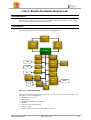
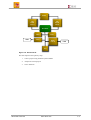
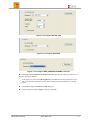
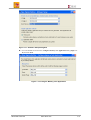
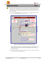
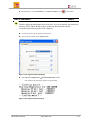
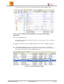
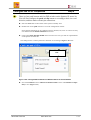
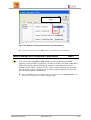
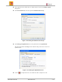
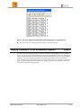
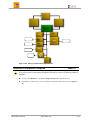
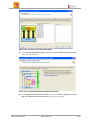
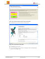
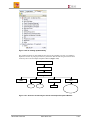
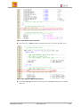
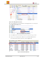
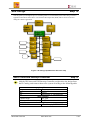
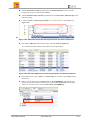
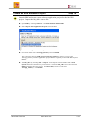
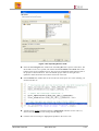
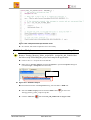
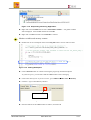
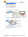
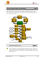
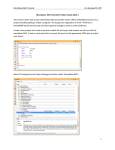
Lab 4: Simple MicroBlaze Hardware Design Targeting MicroBlaze™ on Spartan™-3E Starter Kit Xilinx EDK Tool Lab www.xilinx.com 1-1 Lab 4: Simple Hardware Design Lab Introduction This lab guides you through the process of using Xilinx Platform Studio (XPS) to create a simple processor system targeting the Spartan-3E Starter Kit Procedure The following diagram represents the completed design (Figure 1-1). BRAM LMB BRAM CNTLR LMB BRAM CNTLR MicroBlaze MDM UART LEDs GPIO XPS BRAM CNTLR PSB GPIO BRAM INTC DIP GPIO Timer ICON IBA MPMC CNTLR LCD DDR MYIP PLB Figure 1-1. Completed Design In this lab, you will use the BSB of the XPS system to create a processor system consisting of the following processor IP (Figure 1-2): • MicroBlaze (version 7.1) • PLB_MDM • LMB BRAM controllers for BRAM • BRAM • UART for serial communication • GPIO for LEDs • MPMC controller for external DDR_SDRAM memory Xilinx EDK Tool Lab www.xilinx.com 1-2 BRAM LMB BRAM CNTLR LMB BRAM CNTLR MicroBlaze UART MDM LEDs GPIO MPMC CNTLR DDR PLB Figure 1-2. Processor IP This lab comprises three primary steps: 1. Create a project using the Base System Builder 2. Analyze the created project 3. Test in hardware Xilinx EDK Tool Lab www.xilinx.com 1-3 Creating the Project Using the Base System Builder Step 1 Launch Xilinx Platform Studio (XPS) and create a new project. Use Base System Builder to generate a MicroBlaze system and memory test application targeting the Spartan-3E starter kit. Open XPS by selecting Start → Programs → Xilinx ISE Design Suite 10.1 → EDK → Xilinx Platform Studio Leave the default Base System Builder option and click OK to start the wizard (Figure 13). If you clicked cancel, you can select File → New Project and the same dialog box will appear. Figure 1-3. New Project Creation Using Base System Builder Browse to c:\labs directory, create a new folder called lab4 and select it, and click Open followed by click Save (Figure 1-4). Click <OK>. Figure 1-4. Assigning Project Directory Select the I would like to create a new design option in the Welcome to Base System Builder dialog box and click Next. Xilinx EDK Tool Lab www.xilinx.com 1-4 In the Select Board dialog box, specify the settings below (Figure 1-5) and click Next to continue. ¡ Board Vendor: Xilinx ¡ Board Name: Spartan™-3E Starter Board ¡ Board Revision (Verify on board): D Figure 1-5. Select Board Dialog Box In the Select Processor dialog, leave the default MicroBlaze option (Figure 1-6) and click Next. Figure 1-6. Select Processor Dialog Box In the Configure Processor dialog box (Figure 1-7), leave the default settings (see below) and click Next. ¡ Reference Clock Frequency: 50 MHz Xilinx EDK Tool Lab www.xilinx.com 1-5 o This is the external clock source on the board you are using. This clock will be used to generate the processor and bus clocks. ¡ Processor –bus Clock Frequency: 50 MHz ¡ Debug Interface: On-Chip H/W debug module ¡ Local Data and Instruction Memory – 16 KB ¡ Cache Setup: Enable - unchecked Figure 1-7. Configure Processor Dialog Box Select and configure the LEDs_8Bit, RS232_DCE, and DDR_SDRAM as the only external devices. Generate the memory test sample application and linker script. In the Configure IO Interfaces dialog, select and configure the RS232_DCE, LEDs_8Bit and DDR_SDRAM peripherals as shown below, leaving the rest of the peripherals unchecked. ¡ RS232_DCE: XPS UARTLITE, 115200 baud rate, 8 Data bits, no interrupt, no parity (Figure 1-8) ¡ LEDs_8Bit: XPS GPIO. No interrupt (Figure 1-9) ¡ DDR_SDRAM: MPMC Controller (Multi-Port Memory Controller) Xilinx EDK Tool Lab www.xilinx.com 1-6 Figure 1-8. Configure RS-232 DCE Figure 1-9. Configure XPS GPIO Figure 1-10: Configure DDR_SDRAM with MPMC Controller Click Next until the Add Internal Peripherals dialog is displayed, making sure that none of the other devices are selected At this point you could click Add Peripheral to add additional internal peripherals, but you will see an alternative method in the next lab for adding internal peripherals to an existing project. Click Next to display the Software Setup dialog box. Unselect Peripheral selftest (Figure 1-11) and click Next. Xilinx EDK Tool Lab www.xilinx.com 1-7 Figure 1-11. Software Setup Dialog Box Leave the default selections in the Configure Memory Test Application dialog (Figure 112) and click Next. Figure 1-12. Configure Memory Test Application Xilinx EDK Tool Lab www.xilinx.com 1-8 Verify the system summary in the System Created dialog (Figure 1-13) and click Generate Figure 1-13. System Created Dialog Box Click Finish once the congratulations dialog box appears, indicating the files that BSB has created. In the Next Step dialog box, ensure Start Using Platform Studio is checked and click OK A Software Agreement dialog may appear if this is the first time the software is run A System Assembly View1 will be displayed (Figure 1-14) showing peripherals and busses in the system, and the system connectivity. Figure 1-14. System Created Dialog Box Xilinx EDK Tool Lab www.xilinx.com 1-9 Analyze the Hardware Step 2 Generate a block diagram of the system and study the system components and interconnections. Look in the System Assembly View and analyze the bus and port connections. Run PlatGen to generate the system netlists (NGC) and review the generated files. Click on the Block Diagram tab to open a block diagram view (Figure 1-15) and observe the various components that are used in the design Figure 1-15. Block Diagram View of the Generated Project You can zoom in and out and use the scroll bars to navigate around the block diagram. You will see the MicroBlaze™ processor, LMB controller and PLB bus connected to the MicroBlaze processor. In addition, you will see the I/O ports on the sides and legend at the bottom of the diagram. In the System Assembly View click on plus button and observe the expanded (detailed) bus connection view of the system (Figure 1-16) Xilinx EDK Tool Lab www.xilinx.com 1-10 Figure 1-16. Detailed Bus Connections Click on the Ports filter and have an expanded view similar to Figure 1-17. This is where you can make internal and external net connections. Xilinx EDK Tool Lab www.xilinx.com 1-11 Figure 1-17. Ports Filter Click on the Addresses tab and have an expanded view similar to Figure 1-18. This is where you can assign base/high addresses to the peripherals in the system. Figure 1-18. Assign Base/High Addresses Xilinx EDK Tool Lab www.xilinx.com 1-12 Run PlatGen by selecting Hardware → Generate Netlist or click Test in Hardware No se pu ed in the toolbar Step 3 Generate bitstream and download to the board. Prior to download, the instruction memory (FPGA Block RAM) will be updated in the bitstream with the executable generated using the GNU compiler. Connect and power up the Spartan-3E starter kit Open a hyperterminal session (Figure 1-19) Figure 1-19. HyperTerminal Settings Select Device Configuration g Download Bitstream in XPS. You should see the following output on hyperterminal Figure 1-20. HyperTerminal Output Xilinx EDK Tool Lab www.xilinx.com 1-13 Adding IP to a Hardware Design Lab Step 4 The purpose of this step is to extend the hardware design (Figure 1-21) created according to the following procedure 1. Add and connect GPIO peripherals in the system 2. Configure the GPIO peripherals 3. Make external GPIO connections 4. Analyze the MHS file 5. Add the software application and compile 6. Verify the design in hardware BRAM LMB BRAM CNTLR LMB BRAM CNTLR PLB MDM MicroBlaze GPIO UAR T GPIO Figure 1-21. Extend the System from the previous step Add and Connect GPIO Peripherals to the System Step 5 Add two instances of an XPS GPIO Peripheral from the IP catalog to the processor system via the System Assembly View. XPS provides two methods for adding peripherals to an existing project. You will use the first method, the System Assembly View panel, to add most of the additional IP and connect them. The second method is to manually edit MHS file. Select the IP Catalog tab in the left window and click on plus sign next to General Purpose IO entry to view the available cores under it (Figure 1-22) Xilinx EDK Tool Lab www.xilinx.com 1-14 Figure 1-22. System Assembly View Double-click on the XPS General Purpose IO core twice, to add two instances to the System Assembly View Change the instance names of the peripherals to dip and push, by clicking once in the name column, typing the new name for the peripheral followed by pressing Enter key At this point, the System Assembly View should look like the following (Figure 1-23): Figure 1-23. System Assembly View After Adding Peripherals Click once in Bus Connection column for the push and dip instances to connect them as slave devices to the PLB. Xilinx EDK Tool Lab www.xilinx.com 1-15 At this point, the Bus Connections tab should look like the following (Figure 1-24): Figure 1-24. Bus Interfaces Tab showing Bus Connections to the Added Peripherals Select the Addresses filter You can manually assign the base address and size of your peripherals or have XPS generate the addresses for you. Click under the size column in the push and dip instances, change it to 64K, and hit Enter key Click Generate Addresses (located on the right most end of the tabs) to automatically generate the base and high addresses for the peripherals in the system. The base address and high addresses will change as shown in Figure 1-25 below Figure 1-25. Peripherals Memory Map Xilinx EDK Tool Lab www.xilinx.com 1-16 Configure the GPIO Peripherals Step 6 There are four push buttons and four DIP switches on the Spartan-3E starter kit. You will first configure the push and dip instances according to their sizes and direction, and then make external pin connections. Select the Ports filter in the toolbar of the System Assembly View Double-click on the push instance to access the configuration window Notice that the peripheral can be configured for two channels, but, since we want to use only one channel leave the Enable Channel 2 unchecked. Click on the GPIO Data Bus Width down arrow and set it to 4, you will use 4 push buttons on the Spartan-3E starter kit. The settings for the Common parameters should be set according to Figure 1-26 below. PSB Figure 1-26. Configurable Parameters of GPIO Instance for Push Buttons Next click Channel 1 and set Channel 1 is Bi-directional to False and Channel 1 is input Only to True (Figure 1-27): Xilinx EDK Tool Lab www.xilinx.com 1-17 LEDs Figure 2-7. Setting Configurable Parameters for Push Buttons Set the same parameters for the dip instance, as performed for the push buttons. Make External GPIO Peripheral Connections Step 7 You will connect the push and dip instances to the push buttons and DIP switches on the Spartan-3E starter kit. In order to do this, you must establish the GPIO data ports as external FPGA pins and then assign them to the proper locations on the FPGA via the UCF file. The location constraints are provided for you in this section. Normally, one would consult the Spartan-3E starter kit user manual to find this information. Make the GPIO_in port of the push instance as external by selecting Make External. You should see a new external net connection (Figure 1-28). Xilinx EDK Tool Lab www.xilinx.com 1-18 Figure 1-28. GPIO_in Port Connection Added to push Instance Set the GPIO_in port of dip as external. The GPIO_in ports of both dip and push are now connected externally on the FPGA (Figure 1-29). Figure 1-29. Push and DIP Instances External Ports Xilinx EDK Tool Lab www.xilinx.com 1-19 Click on the system.ucf file under the Project tab and add the following code to assign pins to push buttons (lab4_1.ucf). Figure 1-30. UCF file (pin assignments). Save the system.ucf and close it Add Software Application and Compile Step 8 Edit the existing c program to implement the functionality of push button and LEDs. Compile the program. Click on Applications tab and under Sources, edit the TestApp_Memory.c file. A snippet of the source code is shown in Figure 1-31. This source code is defined from lab4_1.c. Figure 1-31. Snippet of source code. Xilinx EDK Tool Lab www.xilinx.com 1-20 In the Application tab, double-click on compiler options to open the Compiler Options dialogue box. In the Environment tab, select the option Use Default Linker Script. Figure 1-32. Setting the Default Linker Script In the Debug and Optimization tab, set the optimization to No Optimization. This will ensure that the for loop (used for software delay) in the source code is not optimized away. Figure 2-13. Setting the Optimization level Click on Xilinx EDK Tool Lab N o s e to compile the source code. Make sure that it compiles error free www.xilinx.com 1-21 Note: This will automatically run LibGen to generate the required libraries if it has not been done already. Verify the Design in Hardware Step 9 Download the bitstream to the Spartan-3E xc3s500e device. Start a HyperTerminal session Baud rate: 115200 Data bits: 8 Parity: none Stop bits: 1 Flow control: none Connect and power up the Spartan-3E starter kit. Select Device Configuration g Update Bitstream This may take a few minutes to synthesize, implement, and generate the bitstream. Download the bitstream by selecting Device Configuration g Download Bitstream Note: Once the bitstream is downloaded, you should see the DONE LED ON and a message displayed in HyperTerminal as shown in Figure 1-34 Figure 1-34. Screen Shot after the BitStream Downloading After pressing the buttons and toggling the switches, and you should see the corresponding values being displayed on the HyperTerminal (Figure 1-35) Xilinx EDK Tool Lab www.xilinx.com 1-22 Figure 1-35. Push button and DIP switch status displayed on hyperterminal Disconnect and close the HyperTerminal window, and also close XPS Adding Custom IP to an Embedded System Step 9 You will extend the hardware design by creating and adding a PLB peripheral (refer to MYIP in Figure 1-36) to the system, and connecting it to the LCD on the Spartan-3E kit. You will use the Create and Import Peripheral Wizard of Xilinx Platform Studio (XPS) to generate the peripheral templates. You will complete the peripheral by adding LCD interface logic in the templates. Next, you will connect the peripheral to the system and add pin location constraints to connect the LCD controller peripheral to the on-board LCD. Finally, you will verify operation in hardware using the provided software application. Xilinx EDK Tool Lab www.xilinx.com 1-23 Set the GPIO DIP GPIO LMB BRAM Set The the external The GPIO MDM UART PLB LMB BRAM BRA M Figure 1-36. Design updated from previous lab Generate a Peripheral Template Step 10 You will use the Create/Import Peripheral Wizard to create a PLB bus peripheral template. In XPS, select Hardware → Create or Import Peripheral to start the wizard Click Next to continue to the Create and Import Peripheral Wizard flow selection (Figure 136). Xilinx EDK Tool Lab www.xilinx.com 1-24 Figure 1-36. Create and Import User Peripheral Dialog Box In the Select Flow panel, select Create templates for a new peripheral and click Next Click next with the default option To an XPS project selected. Figure 1-37. Repository or Project Dialog Box Click Next and enter lcd_ip in the Name field, leave the default version number of 1.00.a, click Next (see Figure 1-38) Xilinx EDK Tool Lab www.xilinx.com 1-25 Figure 3-4. Provide Core Name and Version Number Select Processor Local Bus (PB v4.6), and click Next Figure 1-39. Select the PLB bus Continuing with the wizard, select User Logic S/W Register support. Select only one software accessible register of 32-bit width. Generate template driver files. In the IPIF Services panel, deselect Include data phase timer and click Next Xilinx EDK Tool Lab www.xilinx.com 1-26 Figure 1-40. IPIF Services Dialog Box Click Next, accepting the default data width, and no burst and cache line support. Click Next to accept default number of registers (one) Figure 1-41. User SW Registers Scroll through the IP Interconnect (IPIC) panel, which displays the default IPIC signals that are available for the user logic based on the previous selection. Click Next Xilinx EDK Tool Lab www.xilinx.com 1-27 Figure 1-42. IP Interconnect (IPIC) Dialog Box In the Peripheral Simulation Support panel, leave Generate BFM simulation platform unchecked, and click Next Figure 1-43. Peripheral Simulation Support Dialog Box In the Peripheral Implementation Options panel, click Generate template driver files to help you to implement software interface, leaving others unchecked Xilinx EDK Tool Lab www.xilinx.com 1-28 Figure 1-44. Peripheral Implementation Options Dialog Box Click Next, and you will see the summary information panel Figure 1-45. Congratulations Dialog Box Click Finish to close the wizard Click on IP Catalog tab in XPS and observe that lcd_ip is added to the Project Local pcores repository (Figure 1-46). Xilinx EDK Tool Lab www.xilinx.com 1-29 Figure 1-46. IP Catalog Updated Entry The peripheral which you just added becomes part of the available cores list. Use Windows Explorer to browse to your project directory and ensure that the following structure has been created by the Create and Import Peripheral Wizard (Figure 1-47) MicroBlaze GPIO LEDs MYIP GPI O LCD PSB Figure 1-47. Structure Created by the Create and Import Peripheral Wizard Xilinx EDK Tool Lab www.xilinx.com 1-30 Create the Peripheral Step 11 Update the MPD file to include the lcd data output of the LCD controller peripheral so the port can be connected in XPS. Add a port called “lcd” to the MPD file. Open lcd_ip_v2_1_0.mpd in the pcores\lcd_ip_v1_00_a\data under lab4 directory. Add following line before the SPLB_Clk port under the Ports section PORT lcd = “ “, DIR = O, VEC = [0:6] Figure 1-48. Update the MPD file for the LCD Controller Peripheral Save the file and close Create the LCD controller using the appropriate HDL template files generated from the Create/Import peripheral wizard: lcd_ip.vhd and user_logic.vhd. You can edit these files using a standard text editor. Open lcd_ip.vhd in the pcores\ lcd_ip_v1_00_a\hdl\vhdl directory. Add user port lcd of width 7 under USER ports added here token (see Figure 1-49) Xilinx EDK Tool Lab www.xilinx.com 1-31 Figure 1-49. Add the User Port LCD Search for next --USER and add port mapping statement, save the file and then close it Figure 1-50. Add Port Mapping Statement Open user_logic.vhd file from the vhdl directory and add lcd port definition in the USER Ports area Xilinx EDK Tool Lab www.xilinx.com 1-32 Figure 1-50. Add the lcd Port Definition Search for next --USER and the enter the internal signal declaration according to the figure below Figure 1-50. Internal Signal Declaration for the User Logic Search for –USER logic implementation and add the following code or copy it from lab_4_2_lcd_user_logic.vhd. Xilinx EDK Tool Lab www.xilinx.com 1-33 Figure 1-51. Add Code Save changes and close the user_logic.vhd Select Project → Rescan User Repositories to have the changes in effect Add and Connect the Peripheral Step 12 Add and connect the LCD peripheral to the PLB bus in the System Assembly View. Make internal and external port connections. Assign an address range to it. Establish the LCD data port as external FPGA pins and assign the pin location constraints so the peripheral interfaces to the LCD display on the Spartan-3E starter kit. In IP Catalog, select lcd_ip core, drag and drop it in the System Assembly View panel Make sure that the Bus Interfaces filter is selected in the System Assembly View and click on the circle in the bus connection diagram to make bus connection (Figure 1-52) Xilinx EDK Tool Lab www.xilinx.com 1-34 Figure 1-52. Making Bus Connection Select the Ports filter, and connect the lcd port of the lcd_ip_0 instance as an external pin by selecting Make External (Figure 3-21) Figure 1-53. Assign the lcd_0 Instance Select Addresses filter and lock addresses of all devices except for the lcd_ip_0 instance. Change the size of the lcd peripheral to 64K and click the Generate Addresses button. Your results should look similar to that below (as shown in Figure 1-54) Figure 1-54. Generate Addresses Xilinx EDK Tool Lab www.xilinx.com 1-35 Modify the system.ucf file to assign external LCD controller connections to the proper FPGA pin locations. Open the system.ucf file by double-clicking the UCF File: data\system.ucf entry under Project Files in the System tab. Copy it from lab_4_2_lcd.ucf Figure 1-55. Adding UCF Constraints Save and close the file Verify the Design in Hardware Step 12 Add a software new software program. Use EDK to generate the configuration file and program the Spartan-3E xc3s500e-4fg320 device. Click on the Applications tab and remove TestApp_Memory.c file from the sources Add lcd.c file in sources Connect the USB and RS-232 cables to the XUP Spartan-3E board and power it up. Start a HyperTerminal with the following settings • Baud rate: 115200 • Data bits: 8 • Parity: none • Stop bits: 1 • Flow control: none From EDK, click on Device Configuration à Download Bitstream to download the system to the FPGA Note: this will perform the following steps Run platgen to generate the netlists Generate the bitstream Run libgen to generate the libraries and drivers Compile the program to generate the executable Update the BRAMs in the bitstream with the executable Download the bitstream to the FPGA Note: Once the bitstream is downloaded, you should see the DONE LED ON and a message displayed in HyperTerminal as shown in Figure 1-55 Xilinx EDK Tool Lab www.xilinx.com 1-36 Figure 1-55. Screen Shot after the BitStream Downloading You should see LCD Test Over in the HyperTerminal window and “MicroBlaze and FPGAs rules” on the LCD panel on the XUP Spartan-3E board Update a Basic Software Application Step 13 Run LibGen to generate xparameters.h file which defines various symbolic parameters. Modify a software program to display the DIP switch settings on the LEDs. Run libgen by seelcting Software → Generate Libraries and BSPs to generate xparameters.h file ¡ LibGen writes the xparameters.h file, which provides critical information for driver function calls. In the Applications tab, remove lcd.c and add lab4_1.c to the TestApp_Memory project You will extend the functionality in lab4_1.c by adding code to display switch settings on the LEDs. Open the GPIO API documentation by right-clicking on LEDs_8Bit peripheral in the System Assembly View and selecting Driver: gpio_v2_12_a g View API Documentation View the various C and Header files associated with the GPIO by selecting File List at the top of the page. Click the header file xgpio.h and review the list of available function calls for the GPIO The following steps must be performed in the software application to enable writing to the GPIO: 1) Initialize the GPIO, 2) Set data direction, and 3) Write the data Find the descriptions for the following functions by clicking links: XGpio_Initialize (XGpio *InstancePtr, u16 DeviceId) ¡ ¡ InstancePtr is a pointer to an Xgpio instance. The memory the pointer references must be pre-allocated by the caller. Further calls to manipulate the component through the XGpio API must be made with this pointer. DeviceId is the unique ID of the device controlled by this XGpio component. Passing in a device ID associates the generic XGpio instance to a specific device, as chosen by the caller or application developer. Xilinx EDK Tool Lab www.xilinx.com 1-37 XGpio_SetDataDirection (XGpio * InstancePtr, unsigned Channel, u32 DirectionMask) ¡ InstancePtr is a pointer to the XGpio instance to be worked on. ¡ Channel indicates the channel of the GPIO (1 or 2) to operate on ¡ DirectionMask is a bit mask specifying which discretes are input and which are output. Bits set to 0 are output and bits set to 1 are input. XGpio_DiscreteWrite (XGpio *InstancePtr, unsigned channel, u32 data) ¡ InstancePtr is a pointer to the XGpio instance to be worked on. ¡ Channel indicates the channel of the GPIO (1 or 2) to operate on ¡ Data is the data written to the discrete registers. Open the header file xparameters.h by double-clicking on Generated Header: microblaze_0/include/xparameters.h under the microblaze_0 instance for the TestApp_Memory project in the Applications tab. Figure 1-56. Double-Click the Generated Header File ¡ In the xparameters.h file, find the following #define used to identify the LEDs_8Bit peripheral: #define XPAR_LEDS_8BIT_DEVICE_ID GPIO Note: The LEDS_8BIT matches the instance name assigned in the MHS file for this peripheral. This #define can be used in the XGpio_Intialize function call. Modify your C code to echo the dip switch settings on the LEDS (Figure 1-57) and save the application. Xilinx EDK Tool Lab www.xilinx.com 1-38 Figure 1-57. Partially Completed C File Click the compile button Xilinx EDK Tool Lab to compile the program. www.xilinx.com 1-39 SDK Design Step 12 This lab guides you through the process of adding timers to an embedded system and writing a software application that utilizes these timers. The Software Developers Kit (SDK) will be used to create and debug the software application. pcores MYIP Select DDR option to store MPMC CNTLR ipwiz.log Note: ipwiz.opt The Readme.txt vhdl data_old PAO lcd_v1_0 0_a PLB MicroBlaze DIP LMB BRAM LMB BRAM INTC devl MPD UART BRA MDM M Timer hdl data Figure 1-58. Design Updated from Previous step Add a Timer and Interrupt Controller Step 13 Add the XPS timer and XPS Interrupt Controller peripherals to the design from the IP Catalog, and connect them to the system according to the following table. plb_clk Intr Irq CaptureTrig0 Interrupt INTERRUPT Xilinx EDK Tool Lab xps_intc_0 instance sys_clk_s timer1 Microblaze_0_INTERRUPT delay instance net_gnd timer1 microblaze_0 instance Microblaze_0_INTERRUPT www.xilinx.com 1-40 Add the XPS Timer/Counter peripheral from the DMA and Timer section of the IP Catalog and change its instance name to delay Add the XPS Interrupt Controller peripheral from the Clock, Reset, and Interrupt section of the IP Catalog Connect the timer and interrupt controller as a ‘s’ (slave) device to the PLB bus (see Figure 1-59) Figure 1-59. Add and Connect the Interrupt Controller and Timer Peripherals Select size as 64K bytes from drop down box and click Generate Addresses. Your results should look similar to that indicated in the figure below. Figure 1-60. Generate Addresses for Interrupt Controller and Timer peripherals In the Ports section, type in timer1 as the Interrupt port connection of the delay instance, and hit enter. Make a new net connection (see Figure 1-61) for the INTERRUPT (external interrupt request) port on the microblaze_0 instance by selecting New Connection from the dropdown box. This will create a net called microblaze_0_INTERRUPT. Xilinx EDK Tool Lab www.xilinx.com 1-41 Figure 1-61. Make a new net connection to connect the MicroBlaze Interrupt port Connect the interrupt controller and timer as follows (refer to Figure 1-60) • Connect interrupt output port Irq of the xps_intc_0 instance to the MicroBlaze interrupt input port using the microblaze_0_INTERRUPT net. • Click in intr field of xps_intc_0 field to open the Interrupt Connection Dialog. Click on timer1 on left side, and click on (right), and then click OK. N o s sign to add to the Connected Interrupts field Figure 1-62. Connecting the Timer and Interrupt Controller • Change the net name of CaptureTrig0 port of delay instance to net_gnd. Figure 1-62. Connections Snapshot between Timer and Interrupt Controller Double-click on delay to open its parameters box and check Only One Timer is Present. Click OK to accept the changes and close the dialog box Select Hardware → Generate Bitstream Xilinx EDK Tool Lab www.xilinx.com 1-42 Create an SDK Software Project Step 14 Launch SDK and create a new software application project for the lab XPS project. Import the lab_sdk.c source file. Open SDK by selecting Software → Launch Platform Studio SDK Select Import XPS Application Projects and click Next. Figure 1-62. Managed Make C Project Put a check mark next to TestApp_Memory and click Finish. This creates the directory SDK_Projects/TestApp_Memory, which is a copy of the TestApp_Memory software application project that was originally created with Base System Builder. Add lab_sdk.c by selecting File → Import. In the Import wizard. Double-click on File System and browse the directory to select them. Check the lad_sdk.c source file and click Finish to add the file to the project. For Into Folder, browse to and select TestApp_Memory. Click Finish Xilinx EDK Tool Lab www.xilinx.com 1-43 Figure 1-63. Importing Source Code In the left hand Navigator tab, double click on the lab_sdk.c file to open it in the editor. The file is built as soon as it is opened, and note that both the Problems and Console tabs on the bottom report several compilation errors. The project is automatically built each time files in the project are edited and saved. Note also that the project outline on the right side is updated to reflect the libraries and routines used in the source file In the Problems tab, double-click on the second red x for the parse error. This will bring you around to the line 86. Figure 1-64. First Error Add the missing global variable declaration as unsigned int, initialize it to the value of 1, and save the file. The first error message should disappear. Click the next error message to highlight the problem in the source code Xilinx EDK Tool Lab www.xilinx.com 1-44 Figure 1-65. Second Error Add the missing global variable declaration as int, inititalize it to the value of 0, and save the file. The additional error messages should disappear. Write an Interrupt Handler Step 15 Create the interrupt handler for the XPS timer. This source code is defined from lab_sdk_ext.c Go to where the interrupt handler function has already been stubbed out in the source file (a fast way to do this is to double-click on the function in the outline view). Create new local variable for the timer_int_handler function: unsigned int csr; The first step in creating an XPS timer interrupt handler is to verify that the XPS timer caused the interrupt. This can be determined by looking at the XPS Timer Control Status Register. Open the API documentation to determine how the Control Status Register works. In the XPS System Assembly View window, right-click the delay instance and select View PDF Datasheet to open the data sheet Go to the Register Description section in the data sheet and study the TCSR0 Register. Notice that bit 23 has the following description: Timer0 Interrupt Indicates that the condition for an interrupt on this timer has occurred. If the timer mode is capture and the timer is enabled, this bit indicates a capture has occurred. If the mode is generate, this bit indicates the counter has rolled over. Must be cleared by writing a 1 Read: 0 - No interrupt has occurred Xilinx EDK Tool Lab www.xilinx.com 1-45 1 - Interrupt has occurred Write: 0 No change in state of T0INT 1 Clear T0INT (clear to ’0’) The level 0 driver for the XPS timer provides two functions that read and write to the Control Status Register. View the timer API doc by right-clicking on the delay instance in the System Assembly View and selecting Driver:tmrctr_v1_10_b g View API Documentation. In the API document, click on the File List link at the top of the document, then click on the link labeled xtmrctr_l.h in the file list. This brings up the document on identifiers and the low-level driver functions declared in this header file. Scroll down in the document and click on the link for the XTmrCtr_mGetControlStatusReg( ) function to read more about this function. Use this function to determine whether an interrupt has occurred. The following is the pertinent information found in the XPS timer documentation: XTmrCtr_mGetControlStatusReg ( BaseAddress, TmrCtrNumber ) Get the Control Status Register of a timer counter ¡ Parameters: o o ¡ BaseAddress is the base address of the device. TmrCtrNumber is the specific timer counter within the device, a zero-based number, 0 -> (XTC_DEVICE_TIMER_COUNT - 1) Returns: o The value read from the register, a 32-bit value Add the XTmrCtr_mGetControlStatusReg function call to the code with the associated parameters. The resulting 32-bit return value should be stored in the variable csr. csr = XTmrCtr_mGetControlStatusReg(baseaddr, 0); Note: Substitute baseaddr with the base address for the delay peripheral. Refer to xparameters.h Complete the Interrupt handler (see Figure 1-66) according to the steps below 1. Test to see if bit 23 is set by ANDing csr with the XTC_CSR_INT_OCCURED_MASK parameter. 2. Increment a counter if an interrupt was taken. 3. Display the count value by using the LEDs_8Bit peripheral and print the value using xil_printf (same functionality as printf with the exception of floating-point handling) Hint: You may use the XGpio_DiscreteWrite () function 4. Clear the interrupt by using the following function call: XTmrCtr_mSetControlStatusReg(baseaddr, 0, csr); Xilinx EDK Tool Lab www.xilinx.com 1-46 Figure 1-66. Completed Interrupt Handler Code Save the file, this should compile the source successully. Add Linker Script Step 16 Remove TestApp_Memory_linker_script.ld file. Assign lab_sdk_LinkScr.ld as the linker script for building the project and compile the application. Click on the C/C++ Projects tab on the left side Right-click on TestApp_Memory and select Properties to open the Properties dialog box (or select Project → Properties from the menu) GPIO Figure 5-11. Software Project In the left hand window of the Properties dialog, select the C/C++ Build item N o Select the Linker Script option and click the delete button ( TestApp_Memory_linker_script.ld script file. s e ) to remove the N o Click the Add button ( Xilinx EDK Tool Lab s e ) and add the lab_sdk_LinkScr.ld file (Figure 1-68). www.xilinx.com 1-47 Figure 1-68. Adding Linker Script Click OK to exit the Properties dialogue which will also recompile the program. Verify Operation in Hardware Step 17 Generate the bitstream and download to the Spartan-3E starter kit. Connect and power the board Select Device Configuration g Program FPGA Select TestApp_Memory.elf the Initialization ELF. Figure 5-13. Selecting executable for BRAM initialization Click Save and Program This will configure the FPGA and you should observe a message on the hyperterminal window indicating the count value. The LEDs should be flickering. Xilinx EDK Tool Lab www.xilinx.com 1-48 Figure 1-70. HyperTerminal Output Debugging Using SDK Step 18 Configure Target Connection Settings On the SDK Menu, select Run → Run… This will present a screen summarizing the existing Launch Configurations Under Configurations, select Xilinx C/C++ ELF Click on New to add a new Launch configuration. Figure 1-71. Setting Up Run Configuration Click on the Run button to establish a connection between the debugger and hardware target You should see output displayed on hyperterminal since the program is running. Xilinx EDK Tool Lab www.xilinx.com 1-49 In the XMD Console view, type ‘stop’ at the XMD% prompt to stop the running process (Figure 1-72) Figure 1-72. SDK’s XMD Console Launch Debugger and debug. On the SDK Menu, select Run → Debug… This will present a screen summarizing the existing Launch Configurations Click on Debug. If a dialog box appears asking you to confirm whether to switch to the Debug Perspective, click Yes This opens the Debug perspective. The debugger is automatically connected to the processor via XMD. The processor will be suspended automatically (breakpoint) at the first statement in main() Click on the Resume button. The application will run Figure 1-73. Resuming an Application Click on the Thread[0] (Running) line in the Debug window (left) and click the Suspend button to suspend operation. Xilinx EDK Tool Lab www.xilinx.com 1-50 Figure 1-74. Suspending a Running Application Right click in the Variables tab and select Add Global Variables … All global variables will be displayed. Select count variable and click OK Right click on count and make sure that Enable is selected Monitor variables and memory content. Double-click to set a breakpoint on the line in lab_sdk.c where count is written to LED Figure 1-75. Setting Breakpoint Click on Resume button to continue executing the program up until the breakpoint. As you do step over, you will notice that the count variable value is changing. Click on the memory tab. If you do not see it, go to Window g Show View g Memory Click the + sign to add a Memory Monitor Figure 1-76. Add Memory Monitor Enter the address for the count variable as follows, and click OK Xilinx EDK Tool Lab www.xilinx.com 1-51 Figure 5-21. Monitoring a Variable Click the Resume button to continue execution of the program. Notice that the count variables increment every time you click resume. GPIO Figure 1-77. Viewing Memory Content of the count variable Terminate the session by clicking on the Terminate button. Figure 1-78. Terminating a Debug Session Close the SDK application Xilinx EDK Tool Lab www.xilinx.com 1-52 HW/SW System Debug Lab: MicroBlaze Step 18 You will extend the system created in the previous lab by adding Chipscope ICON and IBA cores. The IBA core will be added to the PLB bus. You will set trigger conditions in the Chipscope Analyzer software (running on PC) to capture bus transactions when the value of the count variable is written to the LEDs. When the hardware trigger condition is met, you will see that the software debugger stops at the line of code that was last executed. BRAM LMB BRAM CNTLR LMB BRAM CNTLR MicroBlaze MDM UART LEDs GPIO XPS BRAM CNTLR PSB GPIO DIP GPIO BRAM INTC Timer ICON IBA MPMC CNTLR LCD DDR MYIP PLB Figure 1-79. Complete MicroBlaze System Instantiate ChipScope Cores Step 19 Add the ChipScope cores using the Debug Configuration wizard. Configure the device and the design to the following ports, as shown in the Figure 1-80. Setup the trigger to trigger when a certain values are on the PLB address, PLB data, and PLB control bus. Xilinx EDK Tool Lab www.xilinx.com 1-53 Figure 1-80. ChipScope Core Connections Select Debug g Debug Configuration Figure 1-81. Debug Configuration Dialogue Click the Add Chipscope Peripheral... button and select the first option, To monitor PLB v4.6 bus signals (adding PLB IBA). Click OK. Xilinx EDK Tool Lab www.xilinx.com 1-54 Figure 1-82. Add the PLB IBA Click to put a check mark in the Bus Write Data Signals field and set the Select the Number of signal samples you want to collect option to 512. Make sure you have the options selected according to Figure 1-83. Figure 1-83. Setting Basic Debug Configuration Options for the PLB_IBA Click the Advanced tab. Under the User tab, in the Trigger In, PLB Reset and PLB Error Status panel, uncheck the Enable probing system reset and system error signals field and set Match unit type to basic Xilinx EDK Tool Lab www.xilinx.com 1-55 Figure 1-84. Setting Trigger In, PLB Reset and PLB Error Status options Select Extended as the Match Unit Type for the PLB Address and PLB Write Data busses Click OK, and view the Bus Interface noting the newly added Chipscope Cores in the System Assembly View Xilinx EDK Tool Lab www.xilinx.com 1-56 Figure 1-85. Chipscope Cores Automatically added to MicroBlaze System Select Hardware g Generate Bitstream Setup SDK and ChipScope Step 20 Open an SDK project and establish a connection to the target using XMD. Having successfully generated your design it is possible to begin viewing it in operation using the SDK debugger and ChipScope Pro tools. Starting the SDK debugger (Software Debug) Launch SDK: select Software → Launch Platform Studio SDK Click cancel when the wizard opens Delete the existing project that was created in Lab (right-click on TestApp_Memory and select delete – do not delete contents) Import the lab_sdk project: go to File → Import → Existing Projects into Workspace and browse to the lab\SDK_projects\TestApp_Memory. Click OK. Xilinx EDK Tool Lab www.xilinx.com 1-57 Figure 1-86. Importing an Existing Project into SDK With TestApp_Memory selected under Projects, click Finish. With the board connected and powered, select Device Configuration g Program FPGA to update the bitstream with the executable and download the bitstream to the FPGA. Operation should still be the same. Setup the target XMD connection by selecting Run → Run…, and click the Run button Operation should still be the same. Figure 1-87. Specify Project and .elf Location Invoke the debugger by selecting Run → Debug…, and then click the Debug button. The SDK Debugger should now be connected to the target and operation should be suspended (Figure 1-88). Code operation will be halted at the first line following the main( ) routine. Xilinx EDK Tool Lab www.xilinx.com 1-58 Figure 1-88. SDK Debugger Connected to Target via XMD Starting ChipScope Pro (Hardware Debug) Launch the ChipScope Pro Analyzer tool from the program group or desktop icon Click on the Open Cable/Search JTAG chain icon. This will identify the devices on the JTAG chain (Figure 1-89). Click OK to open ChipScope Pro Analyzer with default Trigger Setup and Waveform signal windows. Figure 1-89. ChipScope JTAG Device Order Select File → Import. In the Signal Import dialogue click on the Select New File button. Browse to the sources directory and the select the following chipscope definition and connection file (CDC) C:\lab \chipscope_plbv46_iba_0.cdc and click OK. The CDC file contains signals associated with the PLB core which should now be listed in the Trigger Setup and Waveform signal windows. Perform HW/SW Verification Step 21 Setup the trigger to capture 32 data samples when count values greater than 5 are written to the LEDs. Set M0:TRG0 PLB_RNW bit == 0 by clicking the + sign under M0 and selecting the PLB_RNW bit and changing its value to 0 under Value field Xilinx EDK Tool Lab www.xilinx.com 1-59 Change the Radix of M1 and M2 from binary (Bin) to Hexadecimal (Hex) by clicking on the respective boxes and selecting Hex Set M1:TRIG1 == 8144_0000 (or base address of LEDs_8Bit peripheral) and M2:TRIG2 > 0000_0005 by selecting and adjusting the value box Click the field under Trigger Condition Equation, which opens the Trigger Condition: TriggerCondition0 dialog box. Select M0 and Select M1, and then click OK to close. The Trigger Condition Equation field should now display M0 && M1. Click OK. Set the trigger window depth to 32 and position to 0 Set the Storage Qualification (M0 && M1&&M2) so that you capture count values greater than 5 when written to the LEDs_8Bit peripheral. Your settings should be similar to Figure 1-90. Figure 1-90. Chipscope Trigger Settings Delete all the signals from the Waveform window using [Shift Select] except for PLB_RNW. In the Signals window, select PLB_ABus and PLB_wrDBus and add them to the waveform by right click on each bus and selecting Add To View (see Figure 1-91). Figure 1-91. Chipscope Waveform View Setup Setup the trigger by selecting Trigger Setup → Run. Xilinx EDK Tool Lab www.xilinx.com 1-60 Run Software debugger and wait for the condition to trigger In software debugger window (opened before) click on Resume to continue with debug. The ILA core will trigger when a value greater than 5 is written to the LEDs. The buffer will be filled with 32 data samples, which will be displayed in Chipscope-Pro Analyzer (see Figure 1-92). LEDs LCD PSB Figure 1-92. Chipscope-Pro Debug Results Stop the debugger in SDK Close SDK, XPS, and ChipScope programs Xilinx EDK Tool Lab www.xilinx.com 1-61