1
OCTOBER 1982
HEWLETT-PACKARD JOURNAL
(M) ****** GRAPHICS
PLOT ******
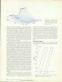
MOSFET ID AND 6M VERSUS V6S
I
D
G
M
C A> CURSOR (-2. 528 i V 19.67nA Ã.8SE-03) (S >
STORE
4.303
E-03
RECALL
4303
/div
I- . 000©
IE- 1
-1 ,00«
QRAD 1 /GRAO
LINE I 8.97E+00 Ã12E-03
LINE2
-1 .67E*00
© Copr. 1949-1998 Hewlett-Packard Co.
HEWLETT-PACKARD JOURNAL
Technical Information from the Laboratories of Hewlett-Packard Company
OCTOBER 1982 Volume 33 • Number 10
Contents:
Intelligent Instrument Streamlines dc Semiconductor Parameter Measurements, by
Kohichi Maeda, Jin-ichi Ikemoto, Fumiro Tsuruda, and Teruo Takeda Curve-tracer mea
surements take a quantum leap forward in accuracy and ease of use.
Programmable Stimulus/Measurement Units Simplify Device Test Setups, by Susumu
Takagi, Hiroshi Sakayori, and Teruo Takeda Each SMU can be electronically set to supply
a specified voltage or current and to measure the associated current or voltage.
HQMOS: Szeto, High-Performance NMOS Technology, by Horng-Sen Fu, Roger To-Hoi Szeto,
Anders and Dejenfelt, and Devereaux C. Chen Smaller NMOS devices operate faster and use
less power. Some process innovations are required to make them.
MOS Device and Process Design Using Computer Simulations, by Soo-Young Oh The
effects of design changes can be accurately predicted by the proper computer model, elimi
nating the need for actual fabrication.
In this Issue:
Semiconductor diodes and transistors are the building blocks of the electronic marvels
I that make our lives easier, more interesting and more productive. The semiconductor is
usually silicon, the main component of beach sand, artfully doped with impurities
to give a desirable electrical properties. Sometimes diodes and transistors come one to a
package as discrete components, and sometimes many are combined in an integrated circuit
on a single chip of silicon. In this age of VLSI — very large-scale integration — there may be
hundreds of thousands of these devices on a chip, forming a complete microcomputer, mem^* ^ " -'» ory, or other functional system. Integrated circuits begin their lives as wafers of silicon. Dozens
or hundreds of circuits are formed on each wafer in a series of processing steps, and then the wafer is cut apart
into assembled chips, which are put into packages ready to be assembled into electronic equipment. On our cover
this month you can see a wafer and a variety of packaged devices.
The instrument pictured on this month's cover is the 4145A Semiconductor Parameter Analyzer. It's a
powerful tool designed to make measurements on transistors and diodes and tell semiconductor manufacturers
some of the things they need to know to improve device performance and increase yields (yield is the percentage
of chips that operate correctly when they're completed). Parameter measurements are also needed by users of
semiconductor devices, who have to know how a device will behave in a circuit, and by people developing
computer models of devices for use in computer-aided design systems. The 4145A resembles a venerable
instrument called a curve tracer, which has been used for twenty years to measure transistor parameters.
However, automatically resemblance is slight, because the 4145A has a built-in microcomputer and can automatically
execute measurement sequences and perform calculations. It can also operate under computer control as part
of an measure test system. Engineers who have used a ruler to measure distances on a curve-tracer's screen
so they could calculate the slope of a trace are impressed when they find they can position two markers on the
41 45A's display and see the slope displayed on the screen. This slope function and the 41 45A's ability to display
calculated parameters are illustrated in the cover photograph. You can get capability like the 41 45A's elsewhere,
but only measurement applications. sophisticated, expensive system that really represents overkill for many measurement applications.
The complete story of the design of the 4145A is on pages 3 to 20.
On page circuits. is an article about one of the many processes used to make HP integrated circuits. This process is
called scaling for reasons explained in the article, and it was developed by scaling down a standard process,
taking advantage of advances in process technology. The scaled-down process produces transistors that
operate faster and use less power than those of the standard process.
In the article on page 28 you can find an example of the use of computer models to simulate how process
changes effects alter device performance. Using these models, process engineers can predict the effects of
changes without actually making a wafer.
-R. P. Do/an
Editor Photographer. P Dolan • Associate Editor. Kenneth A Shaw • Art Director, Photographer. Arvid A Danielson • Illustrator. Nancy S. Vanderbloom
Administrative Services, Typography. Anne S LoPresti. Susan E. Wright • European Production Supervisor. Henk Van Lammeren
2
H E W L E T T - P A C K A R D
J O U R N A L
O C T O B E R
1 9 8 2
 ®
H e w l e t t - P a c k a r d
© Copr. 1949-1998 Hewlett-Packard Co.
C o m p a n y
1 9 8 2
P r i n t e d
i n
U . S . A .
Intelligent Instrument Streamlines dc
Semiconductor Parameter Measurements
Used as a stand-alone instrument or as part of an automated
test system, this smart curve tracer makes it easy to
measure, analyze, graphically display, and store dc
semiconductor parameters.
by Kohichi Maeda, Jin-ichi Ikemoto, Fumiro Tsuruda, and
Teruo Takeda
PRECISE DEVICE PARAMETER MEASUREMENTS
are essential for computer-aided design and
semiconductor research and development, for real
time feedback on wafer evaluations to improve the
semiconductor process and increase yields on the produc
tion line, and for incoming inspection by end users of
semiconductor products. The need for an instrument capa
ble of such measurements that can be used by itself or can be
easily incorporated into an automated test system is becom
ing more and more acute.
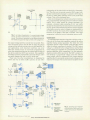
The HP 4145A Semiconductor Parameter Analyzer (Fig.
1) was developed to provide an attractive alternative to a
curve tracer or an expensive test system, and to satisfy the
measurement and evaluation needs of the semiconductor
industries. It is a fully automatic, high-performance in
strument designed to measure, analyze, and graphically
display the dc parameters and characteristics of diodes,
transistors, ICs, solar cells and semiconductor materials.
In stand-alone use, the 4145A can rapidly and accurately
evaluate a complete range of parameters such as threshold
voltage (VT), transconductance (gm), common-emitter cur
rent gain (!IFE)> Early voltage (VA), and many others. See
pages 6 and 10 for examples of typical applications. All of
the necessary stimulus, measurement, calculation, display,
and data storage facilities required are contained in the
4145A. Because the 4145A uses the HP-IB and HP-GL
(Hewlett-Packard Graphics Language), it is easy to interface
the 4145A to other measuring instrumentation and control
lers for laboratory automation. Publication-quality hard
copies of the measurement results displayed on the 4145A's
CRT can be obtained simply by connecting an HP-IBcompatible plotter/printer such as the HP 74 70 A Graphics
Plotter and pressing the PLOT or PRINT keys. The plots for
the application examples discussed on pages 6, 7, 10, and
11 were obtained in this manner. No controller is needed.
However, by connecting a controller and using simple
HP-GL commands, additional information (notes, com
ments, overlay plots, et cetera) can be displayed on the
4145A's CRT, or the CRT can be used as an independent
graphics display.
•Hewlett-Packard Interface Bus, HP's implementation of IEEE Standard 488 (1978)
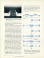
Fig. 1. The HP 41 45 A Semicon
ductor Parameter Analyzer is the
first stand-alone instrument capa
ble of fully automatic measure
ments of dc semiconductor
parameters. Using the HewlettPackard Interface Bus (IEEE 488),
it can also form pan of a larger
computer-controlled test system
for parameter evaluation, com
parison, and storage.
OCTOBER 1982 HEWLETT-PACKARD JOURNALS
© Copr. 1949-1998 Hewlett-Packard Co.
Features
Some of the features of the 4145A are:
• Four stimulus/measurement units (SMUs) that can be
programmed to perform in one of three different modes:
1. Voltage source and current monitor (V mode)
2. Current source and voltage monitor (I mode)
3. Common connection (COM mode).
• Two voltage sources (VS) that can be linearly or logarith
mically swept over their programmed output range.
• Two voltage monitors (VM).
• High-resolution digital CRT display module for display
ing graphic and alphanumeric information in any of five
different display modes: graphic display, matrix display,
schmoo plot, list display, and time domain. The display
can also be programmed by an external controller using
HP-GL commands.
• Internal flexible disc drive for storing measurement
setups, autosequence programs, and data.
• Built-in HP-IB interface for easy connection of the 4145A
to other HP-IB-compatible instruments and controllers to
form automated test systems.
• Eight built-in functions to simplify control and manipu
lation of the displayed data.
• Two user functions that allow front-panel programming
of two different arithmetic operations for calculating
parameters from measured values. The results can be
displayed in real time versus the measured values.
• Versatile front-panel keyboard for measurement setup
and manipulation of displayed data. Eight softkeys along
the right side of the display make it easy for an operator to
select the desired test conditions and display format.
*A three-dimensional plot in which Z-axis values are indicated by different symbols on an
X-Y plot.
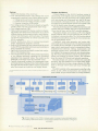
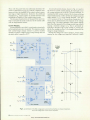
Hardware Architecture
A block diagram of the 4145A's hardware system is
shown in Fig. 2. The digital system is functionally divided
into six blocks: the main processing unit, graphic display
unit, mass storage unit, front-panel unit, and HP-IB inter
face contained in the digital section, and the SMU control
ler located in the measurement section and coupled to the
rest of the digital system through an optoisolator.
The main processing unit uses a 68BOO microprocessor and
contains 16K bytes of ROM, 32K bytes of dynamic RAM, a
10-ms interval timer, and the SMU controller interface.
The graphics display unit contains an HP 1345A Digital
Display Module1 and a two-port read/write 4K x 16-bit vec
tor memory to store picture data. The 1345A picture data is
refreshed automatically by scanning the vector memory at a
rate of approximately 50 Hz.
A keyboard, rotary pulse generator, and various indi
cators make up the front-panel unit. The keyboard consists
of a number of keys arranged in convenient groupings for
page control, measurement control, autosequence control,
integration-time selection, editing, alphanumeric and
arithmetic operation entry, autocalibration, print/plot con
trol, softkeys, file storage and retrieval, and cursor position
ing. The rotary pulse generator outputs 120 pulses per rev
olution and controls the display marker. The indicators
show the current HP-IB status and selected operations.
The mass storage unit contains a flexible disc controller
and drive. The drive handles 5.25-in, single-sided, singledensity, flexible discs having a storage capacity of 92 kilo
bytes on 40 tracks with 9 sectors per track, 256 bytes per
sector.
The SMU controller is the measurement controller in the
4145A. It uses a 6802 microprocessor and contains 12K
bytes of ROM, IK byte of static RAM, two analog interfaces,
Digital Section (Grounded)
Main Processing Unit Mass Storage Unit Front-Panel Unit Graphics Display
Measurement Section (Floating)
Fig. of section diagram of the 4145A's hardware system consisting of a grounded digital section
and a the measurement section. Communication between the two sections is through an
optoisolator.
4 HEWLETT-PACKARD JOURNAL OCTOBER 1982
© Copr. 1949-1998 Hewlett-Packard Co.
and an asynchronous communication interface capable of a
data transmission rate of 250.000 bits s. The two analog
interfaces are used to communicate with the four SMUs.
two VSs, and two YMs via analog-to-digital and digital-toanalog converters as shown in Fig. 2. The asynchronous
interface is ground-isolated and connected to the system
microprocessor in the main processing unit by optoisolators. This arrangement allows floating-ground mea
surements.
The SMU controller has intelligent functions that enable
the system processor to give commands or get data with
ease. For example, it has sweep control capability. Once the
SMU controller has been given sweep parameters (linear/
log, start value, step size, number of steps), it sets up the
source output values, gives hold or delay time, measures
monitored values, and reports measurement data automati
cally at every step.
A second feature is the line-frequency-synchronized
sampling and averaging technique to reduce ac line noise.
When INTEG TIME is set to SHORT, the measured data is
stored directly without integration. However, when INTEG
TIME is set to MED, 16 samples are taken during one ac line
frequency cycle and averaged for each measurement value.
The LONG setting averages 256 samples taken during 16 ac
line cycles. The sample timing is controlled by a timer that
counts the main processing unit clock pulses.
Another feature is SMU dc offset correction. The SMU
controller calibrates all dc offsets in the SMUs and cancels
these parameters on every setting and measurement. Con
sequently there are no adjustable components on the SMU
assemblies. This improves the long-term stability of the dc
offset error specification.
The SMU controller also has a self-test function. Self-test
consists of two parts. One is the test of the SMU controller
itself and the analog-to-digital and digital-to-analog con
verters interfacing the SMU controller to the SMUs, and the
other is the SMU test. If an error occurs in the former test,
the SMU controller shuts down operation because this kind
of error is a fatal error. The system processor detects this
state and displays AOi on the CRT, indicating that the SMU
controller is down. The light-emitting diodes (LEDs) on the
SMU controller board show the error number, which indi
cates the error block. In the SMU test, detected errors are not
fatal to system operation. The SMU controller simply re
ports the results of the test and system operation continues.
At this time, the CRT display shows the error number, if
any, for each SMU.
The measurement section is divided into seven blocks
(excluding the SMU controller): an analog-to-digital con
verter (ADC), a digital-to-analog converter (DAC), four
SMUs, two VSs and two VMs. The 16-bit ADC is combined
with a 10-channel multiplexer. The multiplexer selects one
channel from the 10 channels connected to the four SMU
voltage monitor outputs, the four SMU current monitor
outputs and the two VM outputs. Digital data from the ADC
is sent to the digital section to be processed and displayed.
To obtain both high resolution and high speed from a
simple hardware configuration, the ADC in the 4145A uses
a special input range expansion technique. As shown in the
block diagram in Fig. 3a, the ADC is of the successive
approximation type. It uses two DACs. One is a 14-bit
Digital Output
(Raw Data)
Range 1
Range 2
lo.
Range 3
I03--
(b)
(c)
Time
Fig. 3. (a) Block diagram of the ADC used in the measure
ment section ofthe4145A. The conversion is done by succes
sive approximation, using DACs to supply the error signal
to the error (b) By setting I01, 102, and I03 in turn, the error
signals to correct the offset of the ADC can be derived, (c)
Relationship of the voltages V1 , V2, and V3 shown in (a) for
the first sample-and-hold period.
monotonic main DAC and the other is an offset DAC for
input range expansion. The offset DAC outputs three offset
current values that provide three expanded ranges. Within
each range, the main DAC has 14-bit resolution. The raw
digital data is output as 2 bits of offset range data plus 14
bits of main data. To convert this intermittent binary data
into consecutive data over the full input range, the micro
processor has to know the offset value for each range.
To measure these offset values, a self-calibration is per
formed. First, the main DAC's output current Im is set to
zero and the offset DAC's output current I0 is set to I01 (see
Fig. 3b). At this time, the sample-and-hold circuit is set to
the sample mode and a ramp voltage is applied to its input.
The comparator output goes high at the balancing point
(i.e., V21/R = I01). At this moment, the sample-and-hold
circuit is set to the hold mode. Then the output current of
the offset DAC is changed to I02, and a successive approxi
mation conversion is performed using the main DAC. The
result of this conversion gives the relative offset value be
tween I01 and I02. Similarly, the second step of the calibra
tion process determines the difference between the I02 and
Io;i values of the offset DAC. In addition, the absolute offset
value can be measured by the normal analog-to-digital con-
OCTOBER 1982 HEWLETT-PACKARD JOURNAL 5
© Copr. 1949-1998 Hewlett-Packard Co.
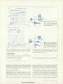
Typical Applications of the 4145A Semiconductor
Parameter Analyzer
Four examples of common semiconductor device measure
ments done by the4145A are shown in Fig. 1 through Fig. 4. The
first trans examples evaluate characteristics of a bipolar npn trans
istor and the remaining two examples evaluate an MOS device.
Part (a) of each figure is a hard copy of the 4145A's graphic
display and part (b) shows the 4145A test connections and SMU
mode settings to the device under test.
Static Collector Characteristics
The static collector characteristics of a bipolar transistor are shown
in Fig. 1. They were obtained by linearly sweeping the collector
voltage VCE from 0 to 10V at five different values of base current IB
and measuring the resulting collector current lc. SMU-1 is pro
grammed for operation as a common source (COM mode), to
which all other sources in the measurement are referenced.
SMU-2 the used as a variable current source (I mode) to provide the
requisite base current. SMU-3 acts as a variable voltage source (V
mode) and current meter to provide collector voltage and mea
sure the collector current. SMU-3 is the primary sweep source
VAR1 and SMU-2 is the secondary, or dependent, sweep source
VAR2. The VAR2 source is incremented only after each VARI
source a By using the 41 45A's built-in line function to draw a
straight line between points A and B, the transistor's collector
output resistance and Early voltage can be read directly from the
1/GRAD and X-INTERCEPT values, respectively. In this example, the
output resistance is 9.37 kfi and the Early voltage is -77.7V.
hFE-lc Characteristics
By using one of the two internal user functions, a bipolar tran
sistor's hpE-lc curve can be obtained (Fig. 2). hpE ¡s defined as
IC/IB. The hFE decay constant can be read directly from the
4145A's CRT display by using the line function to draw a line
tangent to the linear portion of the curve as shown in Fig. 2a.
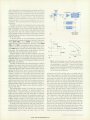
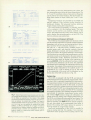
MOS Threshold Characteristics
The five curves shown in Fig. 3 represent an MOS device's
characteristics at five different substrate voltages VSB. The
threshold voltage VTof an enhancement-type MOSFET is defined
as the of voltage required to cause a predetermined value of
drain current (in this example, 10 ¿/.A). VT can be obtained by
vol ****** GRAPHICS PLOT ******
VCF: - i r
1C
<inA> CURSOR C 8. 0000V , 9.151«>A ,
| MARKER C 1. 0000V '
10.00
SMU-3
SMU-2
SMU-1
(COM Mode)
G R A D_ _ [ 1 / G R A D p ( l n t . r - o  « p t
I I 1 B 7 E - 0 6 I 9 . 3 7 E * 0 3 M 7 . 7 E + B B I 8 . 3 l Z E :-0s
ILIMEEI
( a )
it
" ^
Fig. 1 . (a) Linear graphics display
for static collector characteristics
measurement of an npn bipolar
transistor. Cursor is at point B,
marker at point A. (b) Source setup
values and test configuration for
(a).
I****** GRAPHICS PLOT ******
HFE - 1C
HFE
C > CURSOR C 2.333uA , 67. 0E+00,
SMU-3
/dl
SMU-2
1E-01
1E -12
(a)
H F E
1C
C
J
-
1E*00
d . O Q d . / d i V
C
A )
I C / I B
6 HEWLETT-PACKARD JOURNAL OCTOBER 1982
© Copr. 1949-1998 Hewlett-Packard Co.
SMU-1
Fig. 2. (a) hFE versus lc display
for a npn bipolar transistor. Both
axes are logarithmic, (b) Source
setup values and test configura
tion for (a).
I****** GRAPHICS PLOT ******
SUBTHRESHOLD CHARACTERISTICS
SMU-3
S
M
U
-
2
|
D
'
V
D
Ã̄
v -o • |d(SMU'1
COM Mode)
1 . 0 0 0 / d l v
<
(b)
V >
****** GRAPHICS PLOT ******
/ao> - VD
C U R S O R
C
2 .
8 S 0 0 V
,
MARKER < 6.1000V . 93. 8E
1 1 .
5 E - 0 3 ,
^
Fig. 3. faj Log-linear display of
MOSFET threshold characteristics
for five different substrate volt
ages, (b) Source setup values and
test configuration for (a).
>
1 0 0 . 0
E-03
10.
SMU-3
.0000..
.0000
10.00
VD
1 . 0 0 0 / d l v t V >
l/BRAD }< lnt.ro.pt Ylnt«ro«gt j
(COM Mode)
i.2. PEV00J 2.'i7É'*00^T:siÃ6E-03 1
moving the display marker along the curve until ID = 10 /xA (point
A), and then reading the value VG at that point as displayed
numerically above the graph. In Fig. 3, VTO (VSB = 0) is 2.213V.
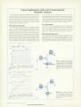
Threshold Voltage VT
Another method of measuring VT is to bias the MOSFET such
that the gate and drain are always at the same potential and
measure the characteristics ¡n the saturation region. Drain current
in the saturation region is calculated as
Fig. 4. (a) Linear display for de
termining threshold voltage of an
MOS device (see text). Cursor is at
point A, marker at point B. (b)
Source setup values and test con
figuration for (a).
where /3 is the gain factor of the device. By taking the square root
of this equation, we find that the relationship between Vi^ and
VGS is linear, the slope of the line is V/3, and the point at which
the line crosses the X-axis is VT. Thus
= N//3 (VGS - VT)
The 4145A's user function can be set up to perform this calcula
tion a the measurement. From Fig. 4, X-INTERCEPT shows a
VT of 2.17V. The square of the line GRAD ¡s/3=566 x 10~6.
I0 = /3(VGS - VT)
version of zero input, which is shown in Fig. 3b as I02. From
these values, the microprocessor is able to determine the
absolute offset value of each range, and to get true data by
simple addition or subtraction. Thus, this ADC can measure
approximately ±11 volts full scale with 0.5-mV resolution
and 200-/XS conversion speed.
The 16-bit DAC is used by the SMU controller to output
control settings. It has a 10-channel distributor that allo
cates outputs from the DAC to each SMU and VS input.
The four stimulus measurement units are the heart of the
4145A. Each SMU can be programmed to function as a
voltage source and current monitor (V mode) or a current
source and voltage monitor (I mode). In the V mode, an
SMU can supply from ±1 mV to ±100V over three output
ranges as given in Table I. In the I mode, currents as low as 1
p A and as high as 100 m A can be forced as listed in Table II.
If higher currents or voltages are required, an SMU can be
used to program an external power supply (see box on page
10). One advantage of the SMU concept is that a fourterminal device can be completely characterized by the
4145A without changing connections. For example, a bipo
lar transistor can be characterized in common-base,
common-collector, and common-emitter configurations
without any connection changes. See the article on page 15
OCTOBER 1982 HEWLETT-PACKARD JOURNAL?
© Copr. 1949-1998 Hewlett-Packard Co.
Table I
SMU Output Capability: V Mode
Voltage
Range
Resolution
Accuracy
±20V 1 mV ±(0.1% of reading
±40V 2 mV +0.05% of range
±100V 5 mV +0.4ÜXIJ
Level o
Maximum
Current I0
100 mA
50 mA
20 mA
I0=output current at set voltage.
'--T
HP-IB Input
Task
Level 1
T
ASP
Interpreter
Task
Level 2
r
Keyboard
Analysis
Task
Page Control
Tasks
r -n
Plot/Print
Task
Analysis
Task
Table II
SMU Output Capability: I Mode
Fig. 4. The software architecture of the 4145A is based on a
real-time monitor to control the utilities and four priority levels
of tasks (ASP=Autosequence program).
V0=output voltage at set current.
for a discussion of the design of the SMUs.
As mentioned earlier, the output from each SMU is de
termined by two input control voltages from the 16-bit DAC,
one for output voltage and one for output current. Other
information, such as voltage or current ranging, is given
directly by the SMU controller. Each SMU outputs two
monitor voltages to the 16-bit ADC that correspond to SMU
output voltage and output current.
The two additional voltage sources (VS) and two voltage
monitors (VM) are built in for measurements that require
more sources and/or monitors than provided by the four
SMUs. EachVS is a programmable voltage source whose ±1
mV to ±20V output is determined, like the SMUs', by the
output from the 16-bit DAC. Each VM is similar to a buffer
amplifier whose monitor output is sent to the ADC via the
multiplexer. Each VM can measure voltages from ±100 /¿V
to ±2V, or from ±1 mV to ±20V. depending on its range
setting.
Software System
The 4145A's software system (Fig. 4) is based on a real-
time monitor whose functions are as follows:
• Task management (multitasking). A task is the primary
structure of an execution environment under the real
time monitor. The monitor supports multitasking opera
tions with four priority levels. Eight tasks are available
for each level. Task management services include start,
end, and abort.
• Task synchronization. Tasks can communicate informa
tion to another task via an event control block, which is
managed by the real-time monitor and not visible to a
task programmer. The receiving task calls the WAIT macrocommand with the event control block number. The
sending task calls the POST macro with the event control
block number and a post code.
• Program management. Certain tasks are resident on the
flexible disc. If one of these tasks is required but is not
already in the overlay area (see Fig. 5), the program man
ager loads the appropriate file containing the task and
starts it.
• Timer services. The real-time monitor can periodically
initiate execution of a specified task. This is a very impor
tant function for measurement instrumentation. The
monitor can also suspend task execution for a specified
interval and initiate execution of a specified task after a
specified interval.
• Interrupt handling. The interrupt handler monitors and
processes interrupts from the powerfail detector, timer,
HP-IB, and asynchronous communication interface. Up
to eight interrupt processing routines can be supported.
• I/O control. The I/O control subsystem provides the basic
drivers and various utilities to control the instrument
hardware, graphics display, mass storage, front panel,
and asynchronous communication interface.
The 4145A has a memory-mapped I/O system and 16K
8 HEWLETT-PACKARD JOURNAL OCTOBER 1982
© Copr. 1949-1998 Hewlett-Packard Co.
OOOOHI
System Common
Directory
1000H
Measurement
Control Block
Data Buffer
1COOH
UF Object
and Stack
ASP Object
System Label
2000H
3000H
12 4K-byte
System Files
Overlay Area
(4K)
4000H
System
Resident
Area
(16K)
8000H
Directory
Spare Directory
User Files
143 Records
36.6 kilobytes
COOOH
FFFFH I
(a)
(b)
Fig. 5. (a) Memory map for main processing unit, (b) Disc
memory structure for the single-sided, single-density, 5.25-in
flexible discs used by the 4145A's internal disc drive.
bytes (4KX4) of ROM. The ROM area contains the real-time
monitor, I/O control, power-on self-test programs, and some
frequently used utilities.
The 4145A's memory map is shown in Fig. 5a. The direc
tory is a copy of the directory stored on the disc. If the disc is
changed, the directory is automatically revised at the next
file access. The measurement control block contains the
control information for a measurement. Data in this block is
changed by changing the information on the CHANNEL DEF
INITION, SOURCE SET UP, MEAS & DISP MODE SET UP, OUT
PUT SEQUENCE SET UP and DISPLAY menu pages. This area
(768 bytes) can be stored on the disc by the command SAVE
P Filename. Measurement data is stored in the data buffer
(2304 bytes). The measurement control block and the data
buffer can be stored on the disc by the command SAVE D
Filename. The UF object and stack area (256 bytes) is used as
an intermediate code area for user functions and as a stack
area for RPN (Reverse Polish Notation) operation. The in
termediate code of the autosequence program is resident in
the ASP object area (256 bytes). This area can be stored on
the disc by the command SAVE S Filename. Nonresident
tasks and data are loaded into the overlay area by the real
time monitor before execution. Resident tasks, common
data at utilities are loaded into the system resident area at
instrument power-on.
The 4145A uses an internal single-sided, single-density
flexible disc drive to store system programs, measurement
data and user programs. The disc space is divided into a
system area and a user area (see Fig. 5b). The system area
consists of a system label, 12 system files and a directory.
Files in the user area are organized by an indexed access
method. The size of each system file is 4K bytes, including
tasks, utilities and data. The directory is provided for user
area management \vith a spare directory for backup. The
size of the directory is 2K bytes.
The user area has room for 143 records (256 bytes/record).
The first 12 records are reserved for system default pro
grams. The 4145A has three types of user files: program files
(3 records), data files (12 records) and sequence files (1
record). Up to 43 program files can be stored on each disc.
Each file has a unique name (6 characters maximum). The
following commands and the catalog function (see Fig. 6)
are provided for management of these user files.
SAVE P/D/S Filename for storing user files
GET P/D/S Filename for retrieving user files
PURGE P/D/S Filename for purging user files
REPACK for repacking the user area
P indicates a program file, D indicates a data file, and S
indicates a sequence file.
Instrument Operation
There are two important points to consider when design
ing a keyboard- operated instrument. One is simplicity and
ease of use, making the measurement complexity trans
parent to the inexperienced or casual user. The other is
versatility for more experienced users and sophisticated
measurements.
The operating system of the 4145A is designed to perform
a wide range of operations with menu-driven, softkeyoriented control. The measurement procedures are divided
functionally into four parts that are each displayed in a
menu page format: CHANNEL DEFINITION, SOURCE SET UP,
MEAS & DISP MODE SET UP, and DISPLAY (see Fig. 7). These
pages can be accessed sequentially by pressing the PREV or
NEXT keys, and directly from the menu page by pressing the
appropriate softkey. The user sets up, or programs, the
measurement by filling in blanks on each menu page. The
•*-** USER FILE CATALOG -**-*
Lhpl
Fig. disc. Typical directory listing of files stored on a flexible disc.
Each disc contains the operating system for the 4145A in
addition to saved user programs and stored data.
OCTOBER 1982 HEWLETT-PACKARD JOURNAL 9
© Copr. 1949-1998 Hewlett-Packard Co.
Extending the 4145A's Output
Range for Power Transistor Measurements
Each of the 4145A's stimulus/measurement units (SMUs) is
capable of supplying up to 100 mA or ±100V, with a maximum
power and of 2W. This is more than sufficient for stimulating and
measuring low-power semiconductor devices, which account for
perhaps 90% of semiconductor products. To cover the remaining
10%, the consists mainly of power transistors and diodes, the
41 4 5 A 's o u tp u t cap a b i l i ti e s m u s t b e i n c r e a s e d . T h i s c an be ac
complished simply and economically.
The method requires no controller or interface. The only equip
ment needed is the 4145A, its furnished accessories, and a suit
able power supply that can be controlled by an analog voltage
and has a current-monitoring terminal, such as HP's 6024A Autoranging DC Power Supply. Fig. 1 shows the setup.
control voltage Vs. Fig. 3 shows the results of a high-power — over
40W — measurement.
There are several points concerning safety and accuracy that
must be kept in mind when using this method.
1 . Depending on the forward transfer gain hFE of the transistor
under test, current levels up to 10Aare possible with this setup.
Be sure to close the lid of the 16058A Test Fixture before
starting the measurement and do not touch the connection
plate.
2. Because of the high current flow, there will be an unavoidable
voltage drop across the residual resistance of the test leads
and cables. This voltage drop represents a measurement er
ror. The actual collector-emitter voltage VCE is calculated as
6024A
where VOUT is the 6024A's output voltage, I0ui is the output
current, and R is the total residual resistance of the leads,
cables, and test fixture. By using the 4145A's remaining SMU
and one of its voltage monitors for voltage sensing at the
collector and emitter, this error can be reduced to almost zero.
[hp] ****** GRAPHICS PLOT
POWER TR (2N3054)
1C
(A)
Fig. 1 . fes? configuration using HP 6024A Autoranging DC
Power Supply controlled by the 4145A's SMUs, effectively
boosting the output current and voltage range of the 4 1 45 A for
power transistor measurements.
Three of the 4145A's SMUs are used. SMU-2, programmed to
function as a variable current source, drives the base of the
transistor being measured. SMU-1 , programmed to function as a
variable voltage source, is connected to the 6024A's remote
control (analog programming) terminal A2 to provide the voltage
necessary to control the 6024A's output voltage. Output voltage
from the 6024A is directly proportional to the voltage (Vs) supplied
by SMU-1 and can be calculated as
V6024A=12XVS=VCE
(1)
Thus, by sweeping the SMU-1 voltage from 0V to +5V, the
6024A's output can be swept from 0V to 60V. SMU-3, pro
grammed to function as a voltage monitor, is connected to the
6024A's current-monitor terminal A4. The 6024A's output current
is directly proportional to the voltage (V,) measured at this terminal
by SMU-3 and can be calculated as
'6024A-2xV(-lc
\L
(2)
The 6024A's outputs are connected to the collector and emitter of
the transistor as shown in Fig. 1.
By using the two internal user functions of the 4145A to calcu
late the output voltage and current by equations (1) and (2), the
actual values applied to the transistor tested can be displayed
directly. The results of an actual measurement using this setup are
shown in Fig. 2. Maximum current through the transistor is approx
imately 1A and power is close to 1W. Higher current and power
can be the by increasing the base drive current IB and/or the
VCE
.1000/div (V)
1.000
E+00
Fig. 2. Typical graphics display of results obtained with test
setup shown in Fig. 1. Low-voltage VCE characteristics at
collector currents up to 10A are easily shown.
10 HEWLETT-PACKARD JOURNAL OCTOBER 1982
© Copr. 1949-1998 Hewlett-Packard Co.
SMU-4
* * * * * *
1C
GRAPHICS ;
6024A
• Y 500m. HOLD 2S
SMU-3
<A
Fig. 4. Revised Fig. 1 setup to correct for voltage-drop error
introduced by high current flowing through the test leads and
connectors. By measuring the voltage across the transistor
directly, using SMU-4 and VM-1, this error can be eliminated.
VC
4. 200/dlv
Fig. 3. Result of a high-power measurement using the setup
in Fig. 1. The control voltage Vs is swept from 0V to 3.5V in
0.07V steps and IB is swept from 1 mA to 9 mA in 2-mA steps.
To do this, however, the test setup and the user function
calculating VCE must be changed slightly (Fig. 4). SMU-4 is
connected to the collector of the transistor and set up in the I
mode as a constant current source at O.OA with a compli
ance of 100.00V. This allows it to behave as a voltage moni
tor. One of the 4145A's two voltage monitors is connected
field pointer (>) and system messages displayed on the CRT
guide the operator through the programming procedure. If
only minor modifications are desired, the field pointer can
be moved directly to the target field by pressing the appro
priate cursor control keys.
The interactive fill-in-the-blank programming is further
enhanced by the softkey concept. If the 4145A's operating
system were controlled by a conventional keyboard, more
than 200 keys would be needed, or the operator would have
to input commands with alphabetic and numeric keys. The
advantages of using softkeys are that an operator can
quickly select the desired command from softkey prompts,
and all possible commands and functions can be displayed.
Thus, the operator doesn't have to memorize the commands
or refer to a command summary or the manual.
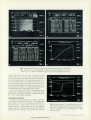
Display Modes and Analysis Functions
Measurement results can be displayed in one of five
different formats.
• Schmoo Plot (Fig. 8a). A three-dimensional (XYZ) dis
play in which five level-dependent, weighted symbols
indicate the relative values of measurement results on the
Z-axis. The symbol at any selected X-Y measurement
point can be highlighted by the cursor function to pro
vide direct numeric readout of the Z-axis value.
• Matrix Display (Fig. 8b). A numerical presentation of a
single characteristic affected by two varying parameters.
For example, hFE can be displayed as a function of base
to the emitter of the transistor and the user function for VCE
is changed from VCE=12xVsto VCE=VM1-VM2.
3. Wait until the transistor has sufficiently cooled before making
additional measurements. Heat generated by high current
flow drastically affects the transistor's parameters, espe
cially hFE and ICB0. Thus, if the measurement is repeated be
fore the transistor has cooled, measurement results will differ
significantly.
4. Set the 4145A to MED or LONG integration time to reduce the
effects of ac line frequency noise on the measurement.
-Michitaka Obara
current Ig and collector-to-emitter voltage VCE. The dis
play can have up to 512 rows of data, corresponding to
steps for variable VARI, and up to six columns per row,
corresponding to steps for the second variable VAR2.
Matrix elements can be measured values or the results of
user-function calculations.
• List Display (Fig. 8c). A complete numeric listing of up to
six parameters and user-function results dependent on
variable VARI.
• Time Domain. The time dependency of semiconductor
parameters can be observed and analyzed. This is done
by not assigning VARI to any of the source channels
(SMUs and voltage sources) on the CHANNEL DEFINITION
page. Measurements over a period as long as 85 minutes
can be made with measurement intervals specified from
10 ms to 10 s. Results can be displayed in graphic, matrix,
or list formats.
• Graphic Display (Fig. 8d). The source variable, mea
surement variables (maximum of six) and user functions
(maximum of two) can be independently assigned to
three axes — X, Yl, and Y2. Therefore, two characteristics
can be displayed simultaneously (double- Y-axis format).
Various display scaling configurations can be specified
independently of the sweep mode of the source variable
(e.g., linear X-linear Yl-linear Y2, or linear-log-linear, or
log-log-log).
The versatility of the graphics display mode is enhanced
by its various analysis functions. The marker function pro-
OCTOBER 1982 HEWLETT-PACKARD JOURNAL 11
© Copr. 1949-1998 Hewlett-Packard Co.
»•»•» CHANNEL DEFINITION «••»«•
(a)
vides readout of not only measurement point values, but
also intermediate point values by linear interpolation. The
X, Yl, and Y2 coordinate values of any point on the graph
can be read by the cursor function. The line function en
ables direct readout of slope (GRAD) plus X and Y inter
cepts.
Comparison functions are provided by the STORE and
RECALL softkeys. They provide overlay displays or
double-axis formats. The autoscale function optimizes
graphic display scaling after measurement.
The zoom function horizontally or vertically expands
(X2) or contracts (X0.5) the displayed graph. The zoom
window can be moved to any location centered on the
cursor. The background area of the vector memory can be
used to display user-oriented graphics via the HP-IB. This
function enhances user applications.
User Functions and Keyboard Arithmetic
(b)
«•» MEAS S. D I SP MODE SET UP
MEASUREMENT MQDF. SWEEP
DISPLAY
MODE.
GRAPHICS
(C)
The 4145A has two programmable user functions which
provide real-time calculation of current- voltage dependent
parameters, such as hFE, gm, and maximum-power hyper
bola. All of the 4145A's arithmetic functions ( + , -, *, /, V,
EXP, LOG, LN, **, ABS, EEX, and A), variables (source and
monitor names only), and physical constants (electron
charge, Boltzmann's constant, and vacuum dielectric con
stant) can be used in the equation defining a user function.
User functions are executed during measurements, and the
calculation results can be displayed in the same manner as
the measurement results. Keyboard calculations can be
made at any time simply by keying in the expression and
pressing EXECUTE. All of the arithmetic functions available
for user-function definitions can be used. Also, keyboard
calculations can be performed in conjunction with the dis
play marker. For example, if the expression Ic/Ig is executed
when the marker (indicated by the symbols • and *) is
positioned at VE=-0.9V as shown in Fig. 7d, the value
of the expression at this point will be displayed on the
bottom line of the CRT (not shown in Fig. 7d).
Systems Use
Fig. 7. Typical measurement setup procedure for the 4145A.
(a) CHANNEL DEFINITION page. The names and source modes
for the SMUs are selected and the names of the voltage
sources and monitors are specified. If required, the user func
tions are defined, (b) SOURCE SET UP page. The range of
values and sweep modes are specified for each source. Delay
and hold times can be specified by pressing the proper
softkeys. (c) MEAS & DISP MODE SET UP page. The desired
measurement and display modes are selected and the ap
propriate display variables are designated, (d) Typical
graphics display for measurement setup example given in
steps (a), (b), and (c).
The 4145A is equipped with the HP-IB, and almost all
measurement functions are remotely programmable. There
fore, the 4145A is a powerful component for a semiconduc
tor measurement system. For more sophisticated users, the
4145A has a special user mode. In this mode, an operator
can control the SMUs, voltage sources and voltage monitors
directly and use the CRT as an independent graphics plot
ter. The operator can use the powerful HP-GL commands
and graphics utilities of HP's desktop computers to build a
user-oriented dc parameter measurement system easily.
The 4145A's PLOT function dumps all information dis
played on the CRT directly onto a digital printer/plotter via
the HP-IB, providing publication-quality hard copies. The
plot area is front-panel programmable and no HP-IB con
troller is necessary. The PRINT function operates similarly,
but only data stored in the measurement data buffer is
printed. The external CRT output allows the operator to
view test results on a large-screen monitor.
Small-scale systemization of the 4145A is possible by
using an analog data link. For example, if you connect a
capacitance meter equipped with an analog output to the
12 HEWLETT-PACKARD JOURNAL OCTOBER 1982
© Copr. 1949-1998 Hewlett-Packard Co.
*******
. 0000V
.0100V
. 0200V
.0300V
,0400V
.0500V
.0600V
.0700V
. 0800V
0 Â ®
* * * * * *
M A T R I X
D I S P L A Y
* * * * * *
LIST
-88 . 90nA
-37.21 HA
-90 . 86HA
-166. 3pA
-268. 4MA
-404. 4MA
-576. 3HA
-790. 7^A
- 1 . 042mA
* * * * * *
DISPLAY
*******
5890V-9 . 988fj
. 5990V 27 . 44p
. 6080V 80 . 85n
.6180V 156.&H
.6270V 258.4^
. 6350V 394 . 3H'
.6430V 566. SM'
.6510V 780. 8M.
.6570V 1 .032m.
G R A P H I C S
P L O T
T EMPER A T U R E
* * * * * *
T R A N SI EN T
E X T N
MEASUREMENT ]
. 0000V - 1 . 08E*e«- 1 . 06E»e«- 1 . 07E.0100V 2.75E.90 3.03E.»* 3.22E.
.0200V 8.12E-08 8.66E*««i 9.02E.
.0300V 15.7E»e» 16.5E*MJ 17.0E.
.0400V 25.8E*M 26.7E»ee 27. IE
.0500V 39.4E*»o 40 . 2E»e* 40 . 0E<
.0600V 56.8E*MJ 56.5E»ee 55 . 5E<
0700V 78. IE»»» 76.2E*»* 73 . 5E<
0 8 0 0 V
1 0 3 E + 0 0
9 8 . 4 E + o e
9 3 . 3 E *
T I M E
4 . 9 9 9 / d i v
C
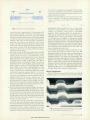
â € ¢ >
Fig. 8. Schmoo of display formats available on the 4145A digital CRT display, (a) Schmoo plot
of hFE versus IB and VCE. (b) Matrix display of data used in (a), (c) List display of IE, VB, and lc
versus transient). at IB = 10.00 /n/A. (d) Graphics plot of hFE versus time (temperature transient).
4145A, you can plot the C-V curve of a device on the
4145A's CRT. In such a measurement, one SMU stimulates
the device under test, which is connected to the capacitance
meter. The analog output of the capacitance meter is con
nected to another SMU or a voltage monitor which mea
sures the analog voltage. The 4145A's user functions can
then calculate and display the capacitance values. By using
the appropriate transducer, you can also handle other phys
ical parameters such as temperature and pressure.
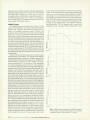
Fig. 9 is an example of a 1-MHz C-V measurement and a
quasistatic C-V measurement made by a system consisting
of the 4145A, HP 4140B pA Meter/DC Voltage Source and
HP 4271B 1 MHz Digital LCR Meter.
******
GRAPHICS
PLOT
******
HF/QUASI -STATIC C-V
Autosequence Programs
The 4145A can be programmed to perform sequential
measurements and output the results. The autosequence
setup shown in Fig. 10 is an automated procedure for
measuring the Ic, IB-VBE, hFE-Ic, IC-VCE and VCE(SAT)
characteristics of a bipolar transistor. The autosequence
program initiates a measurement sequence, activates the
plotter/printer for hard-copy results and then stores the
MCAtUPEMENT ex- ANALYSIS hey
Fig. 9. Sample display of C-V data obtained with the 4145A
and an external capacitance meter and picoammeter/dc volt
age source. The upper curve is the quasistatic capacitance
data and the lower curve is the high-frequency (1 MHz)
capacitance data.
OCTOBER 1982 HEWLETT-PACKARD JOURNAL 13
© Copr. 1949-1998 Hewlett-Packard Co.
*** AUTO SEQUENCE SET UP ***
Call up program from disc
Single sweep
Output CRT display
contents to plotter
Save test results on disc
Allows viewing of results
before output to plotter
Acknowledgments
The authors wish to thank Hiroshi Kanamori and
Hideyuki Hasegawa for developing the digital hardware
and software, Akinori Maeda for power supply design,
Yoshimasa Shibata for mechanical design, Tsuneji
Nakayasu and Akihiko Goto for test fixture and industrial
Advance plotter page
Walt time before execution
of next command
20
21
23
24
Fig. 10. A typical autosequence program for the 41 45A. This
feature allows a user to develop measurement setups, save
them by name on the internal disc unit, and then later call them
back in any order automatically, including plotting and saving
any results.
measurement data on the flexible disc.
Jin-ichl Ikemoto
Jin-ichi Ikemoto received the BS (1972)
and MS (1974) degrees in electrical
engineering from Waseda University.
With Yokogawa-Hewlett-Packard since
1974, he has worked on automatic test
systems in the computer group tor
about three years. Since joining the
R&D lab, he has contributed to the de
sign of the 4191A RF Impedance
Analyzer and designed the main pro
cessing, HP-IB, and mass storage sec
tions of the 41 45A. Jin-ichi is single and
enjoys playing the guitar and swim
ming.
Test Fixture
The 16058A Test Fixture (Fig. 11) is furnished with the
4145A. The 16058A holds the device to be tested and pro
vides all necessary connections to the test input/output
terminals of the 4145A. For stable and accurate measure
ments at extremely low current levels, the 16058A is fur
nished with an electrostatic light-shielding cover. This
cover is also a safety feature to protect users from hazardous
voltages. When the cover is open, output voltages are lim
ited to 42 volts automatically. To facilitate testing various
types of devices, eight interchangeable socket boards and
three types of special plug leads are furnished.
Fumiro Tsuruda
Fumiro Tsuruda was born in
Kagoshima, Japan, and received his
BSEE and MSEE degrees from Tokyo
Institute of Technology in 1972 and
1974. He joined Yokogawa-HewlettPackard in 1977, and worked on the
4140B pA Meter/Voltage Source and
designed the digital section of the
4145A, mainly the software. He enjoys
playing the guitar and the recorder.
Fig. 11. Each 4145A comes
complete with the HP 16058 A Test
Fixture, cables, and connector
plates. Also included (not shown)
are five system discs and a head
cleaning disc.
14 HEWLETT-PACKARD JOURNAL OCTOBER 1982
© Copr. 1949-1998 Hewlett-Packard Co.
Teruo Takeda
Teruo Takeda received his BSEE and
MSEE degrees from Waseda University
in 1976 and 1978. respectively. He
joined Yokogawa- Hewlett-Packard in
1978, and was responsible for the de
sign of the ADC, DAC, and the SMU
controller of the 4145A. He transferred
to HP's Stanford Park Division this past
June to attend Stanford University. He's
married, and enjoys working on audio
equipment and singing.
Kohichi Maeda
Kohichi Maeda received his MSEEfrom
Waseda University, Tokyo, in 1963.
Since joining Yokogawa- HewlettPackard in 1964, he has worked on the
4271A 1-MHz Digital LCR Meter, the
4261 A LCR Meter and the 4274A/
4275A Multi-Frequency LCR Meter. He
served as project manager for the
41 45A. Kohichi and his wife have three
children. Playing tennis is his main rec
reation.
design, and Kazunori Nishitsuru and Hideyuki Norimatsu
for application evaluation. We would like to express our
appreciation to Ulrich Kaempf of HP's Integrated Circuit
Processing Laboratory who introduced us to the SMU con
cept. Special thanks are also due Hamo Ito, our section
manager, who gave us the original idea of the product and
many useful suggestions. To many other people not men-
tioned here who contributed to the product's development,
many thanks.
Reference:
1. K. Hasebe, W.R. Mason, and T.J. Zamborelli, "A Fast, Compact
High-Quality Digital Display for Instrumentation Applications,"
Hewlett-Packard Journal, Vol. 33, no. 1, January 1982.
Programmable Stimulus/Measurement
Units Simplify Device Test Setups
by Susumu Takagi, Hiroshi Sakayori, and Teruo Takeda
EVALUATION OF SEMICONDUCTOR DEVICES and
materials requires an assortment of dc current and
voltage sources and monitors. To connect these to
the device or material to be tested usually requires an array
of cables and a matrix of switches. As such, setting up the
equipment for a particular measurement is often compli
cated and time-consuming. In addition, the nest of cables
and the switch contacts can contribute significant resis
tance, capacitance, inductance, and electrical noise com
ponents that adversely affect measurement accuracy and
speed. To minimize these problems and simplify test
setups, a new approach was chosen for the HP 4145A
Semiconductor Parameter Analyzer — the use of program
mable stimulus/measurement units (SMUs].
Stimulus/Measurement Unit
Each of the four stimulus/measurement units in the
4145A is an independently adjustable, analog-voltagecontrolled dc port that can be programmed from the
4145A's front panel or via the HP-IB to function either as a
voltage source and current monitor (V mode), as a current
source and voltage monitor (I mode), or as a ground refer
ence (COM mode). Also, each SMU can be programmed to
increment or sweep its output.
•Hewlett-Packard Interface Bus, HP's implementation of IEEE Standard 488 (1978),
The main advantage of programmable SMUs is that a
device can be completely characterized using only one
setup. For example, a transistor can be characterized in
common-base, common-collector, and common-emitter
configurations without having to change the physical con
nections between it and the 4145A.
Design Considerations
In designing the 4145A's SMUs, two approaches were
considered: a basic voltage source capable of limiting out
put current and a basic current source capable of limiting
output voltage. The dc characteristics shown in Fig. la are
those of a basic current-limiting voltage source. This volt
age source operates in the current-limit mode when the
voltage setting results in an output current that exceeds the
preset limits. In this mode, the voltage source now behaves
like a current source. In Fig. la, two different loads are
shown: RLI and Rj^. RLI is relatively high, forcing the
source into a constant-voltage. mode, and RLZ is relatively
low, forcing the source into a current-limited mode.
The dc characteristics shown in Fig. Ib are those of a
basic current source capable of voltage limiting. There is no
difference between the two types of sources in normal oper
ation. In the limited operation region, however, there is a
great difference. The voltage source just needs to increase
OCTOBER 1982 HEWLETT-PACKARD JOURNAL 15
© Copr. 1949-1998 Hewlett-Packard Co.
(
a
)
(
b
)
Fig. 1. (a) Output characteristic of a current-limited voltage
source, (b) Output characteristic of a voltage-limited current
source. This source is impractical for real designs because of
the inability to supply very large currents at the voltage limit.
the output voltage until the current limit is reached. How
ever, the current source must be able to clamp the output
voltage with an infinite current source or sink capability. In
real applications, such abnormal conditions can occur
when the current source is incorrectly programmed or
when the connections between its outputs and the pins of
the device under test (DUT) are incorrect. This capability
for infinite current is not feasible in practical designs, and it
can easily damage the load or device under test.
There were two other considerations in designing the
SMUs. One was to obtain stable operation of each SMU
SOkil
or 25 kn | — ^tfV~-]
or 10kil
independent of the other SMUs and the DUT's characteris
tics. The other was to prevent excessive SMU output volt
age that could result in damage to a sensitive DUT. One of
the keys to stable SMU operation is the novel guard filter
scheme. This will be discussed later.
Most circuit designers have observed a partial or total loss
of hFE for transistors operating in the low-collector-current
region. This is often caused by voltage transients. For
example, a transient spike exceeding 25 mV can totally
change the characteristics of some sensitive semiconductor
devices. Some of the methods used in the 4145A to suppress
undesirable excessive output voltages are implemented in
the SMU hardware. But much of the suppression is in the
firmware in the ROMs of the SMU controller. This spike
suppression is effective even at instrument power on/off.
Construction
A simplified block diagram of an SMU is shown in Fig. 2.
Only one of the three error amplifiers controls the power
amplifier during normal operation. The other two error
amplifiers operate in their standby mode and take control
when the output compliance is reached. The SMU output
voltage V0 is buffered by the voltage follower and fed back
to the voltage error amplifier. It is measured by the voltage
monitor amplifier which normalizes it to the analog-todigital converter (ADC) input level. The SMU's output cur
rent develops a proportional voltage across the selected
range resistor which is measured by the current monitor
amplifier after the unwanted common-mode voltage error is
rejected. The output of the current monitor amplifier is also
SMU
Control
Logic
Guard
Filter
SMU Circuit
Common
Float Circuit
and Power
Amplifier Output
Common
16 HEWLETT-PACKARD JOURNAL OCTOBER 1982
© Copr. 1949-1998 Hewlett-Packard Co.
Fig. 2. Simplified block diagram
of one of the four SMUs used in the
4145A Semiconductor Parameter
Analyzer.
normalized to the ADC input level and fed back to the 1+
error amplifier and the I- error amplifier. Five range resis
tors and the selectable gain factor ( x I or x 10) of the current
float amplifier provide the wide output current range (1 pA
to 100 mA) of the SMU with excellent accuracy.
The connection of the SMU output to the DUT is made by
a triaxial cable whose inner shield is connected to the volt
age-follower output so that it surrounds the center conduc
tor with an equipotential field. The outer shield is con
nected to the low-impedance circuit common. This config
uration effectively prevents the SMU output's picking up
undesired noise. This is particularly important in lowcurrent measurements, where the noise level can exceed the
signal level by several decades.
Voltage
Follower
10 nA
10V (=1 GilxlO nA)
Guard Filter
The guard filter is a novel approach implemented in the
4145A SMUs. It contributes greatly to stable, oscillationfree SMU operation, especially in the very-low-current
ranges. Fig. 3 shows a simplified schematic of the output
circuit of the SMUs and the equivalent circuit.
The guard capacitance Cg consists mainly of the capacitive coupling between the center conductor and inner
shield (guard) of the triaxial cable. Y¡' and Yx' in Fig. 3b
represent the additional admittances of Cg that appear
in parallel with the range resistor R¡ and the load Rx, re
spectively. In equation form:
Yx'=jft»Cg[l-F(«)]
(D
Y,'=ja>Cg[F(o))/(l+Av)]
(2)
I
0.1V(=10Mnx10 nA)
T of Q1
(b)
Fig. rang (a) Schematic of soft-switching circuit for current rang
ing with negligible effect on the output voltage, (b) Voltage
relationships for circuit shown in (a) during a range change.
than fT:
(5)
where F(co) is the transfer function of the guard filter and Av
is the open-loop gain of the voltage follower, whose power
supply is referenced to the power amplifier output.
When the guard is connected directly to the voltage fol
lower output, F(OJ) equals 1, and equations (1) and (2)
become
Yx'=0
(3)
Y,'=jo)Cg/(l+Av) « jo
(4)
where f -p is the gain-bandwidth product of the internally
compensated voltage follower. At frequencies much less
The total range admittance Y=(1/RI)-YI' becomes negative
for frequencies above 500 Hz, given a range resistance of
1 Gil, guard capacitance of 500 pF and fT of 1 MHz, for
instance. This means that the feedback component of the
output current is not negative but positive above 500 Hz.
This indicates that stable SMU operation totally free from
oscillation is not possible without changing parameters
that would sacrifice SMU performance (speed, resolution,
et cetera).
The simple low-pass guard filter provides the solution
without degrading SMU performance. At frequencies above
the cutoff frequency fL of the low-pass filter, Y[' and Yx' are
approximated as follows, on the condition that
Y,' =j
^
, v
jcoC.
fe)
Y ' = jo
Fig. 3. (a) Simplified schematic of guard filter, (b) Equivalent
circuit for (a).
(6)
Ã- 1+iüil
(7)
OCTOBER 1982 HEWLETT-PACKARD JOURNAL 17
© Copr. 1949-1998 Hewlett-Packard Co.
Thus, with the guard filter, the additional admittance be
comes a capacitance of Cg^L/ff) without a negative resis
tance and only the feedback of the output current compo
nent lags at high frequencies. Moreover, the additional
capacitance Cg, which appears in parallel with the load,
contributes to stability in the current-control mode.
The low-pass characteristics of the guard filter also func
tion to surround the center conductor of the triaxial cable
with an equipotential surface.
Current Ranging
Current ranging in each SMU is performed automatically
so that optimum accuracy is assured. This requires a spikeless current-range change scheme to prevent sudden
changes of output voltage during a range change that can
adversely affect a sensitive DUT.
A novel soft-switch scheme, shown in Fig. 4, is used in
the 4145A to control current ranging. By turning Ql on or
off, a range resistance of 10 Mil or 1 Gil can be selected. To
maintain the SMU output current at 10 nA when switching
range resistance from 1 Gil to 10 Mil, the voltage across the
range resistor (V0-VF) must change between +10V and
+0.1V as shown in Fig. 4. The maximum change rate of VF
versus time is determined by the response of the voltage
control loop. The range resistance value cannot change
faster than the response of the voltage control loop without
causing a transient change in V0. This is prevented by
applying to the gate of Ql a ramp voltage VG whose slew
rate is slow enough to allow VF to change in step with the
change in range resistance.
During this change, the output voltage V0 is kept nearly
constant by the voltage error amplifier. However, a small
To Power
Amplifier
Input
Vl,n+
1+ Error Amplifier
(a)
Fig. 5. characteris Schematic of the SMU voltage and current control amplifiers, (b) Output characteris
tics of the voltage and current control amplifiers.
18 HEWLETT-PACKARD JOURNAL OCTOBER 1982
© Copr. 1949-1998 Hewlett-Packard Co.
amount of output voltage disturbance is required to supply
the feedback loop current to change VF as calculated by
A\;
=
d V F A V F \ 1
(CfRf) = - I — - ]
d
t
d
t
/
2
7
T
f
v
(8)
where fv is the total gain-bandwidth product of the voltage
control system. In the 4145A the gain-bandwidth prod
uct of the SMUs is 200 kHz and the ramp rate of the soft
switches is 5V/ms. Thus. AV0 is only 4.0 mY.
The ramp signal is referenced to VG or V0, whichever is
more positive, so that a single n-channel FET can handle the
slew-rate-limited current ranging for both directions of
output current.
The current range, which is selectable simply by chang
ing the gain of the current float amplifier (Fig. 2) from xl to
xlO, requires no special circuitry. During current ranging,
a control signal called I Loop Cut is fed back to the
1+ and I- error amplifiers to inhibit their override capability
and ensure SMU control by the voltage error amplifier.
When I Loop Cut is enabled, the other changes inherent to
the current ranging, such as the analog input which must be
changed to correspond with the new range factor, are done
in a predetermined manner by the SMU controller. If the
SMU is operating in a current-control mode before the
change, the input reference voltage Vin is modified step by
step until the SMU reaches its voltage-control mode. At the
instant of detecting the SMU control mode change, the I
Loop Cut signal is asserted and Vin is held constant so that
the current ranging is done at the same (actually a little less
in magnitude) output current.
amplifier and it can no longer control the SMU output
voltage. Then control by the I- or I- error amplifiers is
established and the SMU's output current is proportional
to the voltage Vj. to the I-i- and I- error amplifiers.
The voltage error amplifier Ul is not saturated at this
time, but is operating with a local feedback current is
to prevent saturation of the voltage control loop and va is
set near its control level by twice the diode forward-volt
age drop.
From another point of view, as long as the saturationprevention current is maintained, the voltage error
amplifier is kept ready to control and maintain the SMU
output voltage. All error amplifiers work to maintain the
present output condition. Thus the smooth transfer of
control modes during changes in settings and outputs of
the SMU is assured, preventing overshoot or spikes at the
output.
Automatic Calibration
The monitor functions of the SMU can be used for selfcalibration. Output errors can be compensated by measur
ing the raw errors with the calibrated monitors. All offset
errors of the SMU source/monitor are updated every five
minutes by the normal measurement sequence. Extensive
use of high-stability precision resistors and resistor net
works in the SMU design eliminates the need for gain
adjustments. Because only the single high-performance
DAC and the single high-performance ADC are used to
communicate between all of the SMUs and the SMU con
troller, no individual adjustments are required for each
SMU.
Stability
Control-Mode Change
Each SMU has three control amplifiers. They are the
voltage error, 1+ error and I- error amplifiers and the con
trol modes they monitor are called the V control mode, 1 +
control mode and I- control mode, respectively. One of
them is selected in accordance with the input reference
voltage and feedback signal levels. In each of the SMU
control modes the error amplifiers not used are completely
out of the control loop and do not affect operation. How
ever, they are in a standby condition, ready to take over
SMU control at the instant that the feedback level to any
standby error amplifier is about to exceed its input reference.
Fig. 5 shows a simplified schematic of the voltage, I+, and
I- error amplifiers and their output characteristics. The con
struction of the I + andÃ-— error amplifiers is almost identical to
that of the voltage error amplifier except that the values of the
current sources are appropriate to overridable and one-sided
control, and their outputs are connected to that of the voltage
error amplifier. All three are connected to the input of the
power amplifier, which develops the specified output voltage
or current to the load through the range resistor.
When va (output of Ul) is near zero, the voltage error
amplifier controls the total loop so that the output volt
age is proportional to Vin and the SMU works in its volt
age-control mode. v1 varys from near-zero to maintain the
desired output voltage until it reaches a level equal to two
diode forward-voltage drops. At this time a current is
flows in the internal feedback loop of the voltage error
The dc characterization of semiconductors is sometimes
affected by oscillation. There are two modes of oscillation,
one caused by the SMU, and the other caused by the DUT
and the connection leads. The oscillation caused by the
SMU occurs when an inductive load is connected to the
SMU output. The oscillation frequency is low, less than 300
kHz. The SMU often has an inductive load because the
output impedance of the SMU is inductive in V-mode oper
ation and usually several SMUs are connected to each other
through the DUT.
There are two sources of SMU oscillation, one related
Buffer Amplifier
OUT
(
a
)
(
b
)
Fig. 6. (a) SMU output circuit, (b) Equivalent circuit for (a).
OCTOBER 1982 HEWLETT-PACKARD JOURNAL 19
© Copr. 1949-1998 Hewlett-Packard Co.
VMode
V Mode
Output
(a) I Mode
Fig. 8. A test configuration that could cause SMU oscillation.
It is equivalent to a Hartley oscillator because SMUs operating
in the V mode can act as inductive components.
LrrmJ
L'
Output
(b) V Mode
Fig. 7. (a) Output impedance circuit of SMU in the I mode, (b)
Output admittance circuit of SMU in the V mode.
solely to the output stage of the SMU and the other related to
overall SMU construction when operating in the I mode
(current forcing and voltage sensing). Fig. 6a shows a
simplified drawing of the SMU output circuit. Here, Cg is
the capacitance between the center conductor and the inner
shield of the triaxial output cable. Redrawing Fig. 6a, we
obtain Fig. 6b. If the Q of the Cg-L circuit exceeds unity, this
circuit will oscillate at a frequency of l/27rVCgL. Fig. 7a
shows the equivalent circuit of an SMU operating in the I
mode. The output impedance of this circuit (Zout) is.
oscillate if an unusually large inductance is connected.
This can occur when the DUT is a high-hfe (>3000) transis
tor and the SMU connected to its emitter is set to a lowcurrent range. If oscillation does occur, it is detected by the
oscillation detector in the 4145A and an error message is
displayed on the 4145A's CRT.
The second source of oscillation does not depend on the
structure of the SMU, but on the combination of the DUT
and stray parameters around the DUT, such as load induc
tance and parasitic capacitance. The frequency of this type
of oscillation is rather high, well into the 3-to-30-MHz re
gion. This type of oscillation usually cannot be detected by
the 4145A's oscillation detection circuit. To prevent oscil
lation, we can use ferrite beads on the test leads. If an
unusual display appears, we recommend the use of addi
tional ferrite beads on the DUT leads.
R(l-co0CR) R(,
out
l+(wCR)2 j&j [l+(&jCR)2]
(9)
where OJ0 is the resonant frequency of the system consisting
of two amplifiers. Thus, if &I0CR>1, the equivalent series
resistance of Zout is negative. If an inductive load is con
nected that cancels the equivalent series capacitance
of Zout, this system will oscillate.
What is the chance of being connected to an inductive
load? When the SMU is operating in the V mode (voltage
sourcing and current sensing), the output impedance of the
SMU is inductive (Fig. 7b). When an inductance L is con
nected to the emitter of a transistor, its effect is multiplied
because the base input impedance of the transistor is L
times hfe. Fig. 8 depicts another example. The SMUs con
nected to the MOSFET's gate and drain are operating in the
V mode, so these SMUs appear to be inductive, making this
configuration equivalent to a Hartley oscillator.
To prevent oscillation, the SMU uses a network consist
ing of Cc and Rc as shown in Fig. 6a to compensate for the
output inductive reactance. However, the value of Cc can
not be made large enough to make Zout capacitive because
of the need of a short settling time. Therefore, the SMU may
20 HEWLETT-PACKARD JOURNAL OCTOBER 1982
© Copr. 1949-1998 Hewlett-Packard Co.
Hiroshi Sakayori
P Hiroshi Sakayori earned his BS degree
in electrical engineering from Waseda
University in 1972 and joined
Yokogawa-Hewlett-Packard the same
year. He helped design the SMU and
developed the analog performance test
system for the 4145A. He enjoys moun• tain climbing, skiing and watching Noh
plays in his spare time.
J
Susumu Takagi
Susumu Takagi earned his BS degree
in electrical engineering from Kyoto
University in 1970. He joined
Yokogawa-Hewlett-Packard the same
year as a design engineer. He has
worked on the 1504A/1505A Elec
trocardiograph and the 4140A pA
Meter/DC Voltage Source. He designed
the SMU of the 41 45A. Susumu and his
wife have two sons. He enjoys camping,
woodworking and assembling models
of various kinds.
HQMOS: A High-Performance NMOS
Technology
Innovative processing methods are used to fabricate a
scaled-down version of a standard n-channel MOS process,
resulting in lower power consumption and higher speed.
by Horng-Sen Fu, Roger To-Hoi Szeto, Anders T. Dejenfelt. and
Devereaux C. Chen
SEMICONDUCTOR DEVICE TECHNOLOGY is one of
the most rapidly changing technologies in modern
society. Among major semiconductor device tech
nologies, such as bipolar, MOS (metal-oxide-semiconduc
tor), and III-V or II- VI compounds, MOS has probably ad
vanced the fastest in recent years, especially during the past
decade. Silicon processing technology, on which most
bipolar and MOS devices are based, has emerged as a major
manufacturing technology mainly because of the ability to
grow high-quality silicon dioxide. This greatly reduces de
vice fabrication difficulty. Although III-V and II- VI com
pound technologies have made major progress in recent
years, they still cannot compete with silicon technology
because of material preparation and device fabrication
problems.
Bipolar devices have been traditionally recognized as
superior to MOS devices in speed because of fundamental
differences in device structure and operating principles.
This tradition has changed recently because of advances in
MOS processing that now allow MOS to achieve a faster
access speed than its bipolar counterpart.
Back in 1969, the standard MOS fabrication technology
was an aluminum-gate p-channel process that exhibited
low device density and slow speed compared to today's
MOS circuits. A major breakthrough was the realization of
self-aligned silicon-gate processing. This greatly reduced
the parasitic overlap capacitance between an MOS device's
gate electrode and its source and drain, thus achieving more
speed and improving circuit performance.
Because electron mobility in silicon is higher than hole
mobility, n-channel MOS devices are faster than p-channel
MOS devices using today's shorter device channel lengths.
The use of n-channel technology and the introduction of the
depletion-mode device as an active load were two other
steps toward high-speed MOS devices. Perhaps the most
recent advance in MOS circuit performance has been the
development of device scaling theory. 1 Reducing the size of
an MOS device gains the advantages of shorter propagation
Boron Implant ^ Photoresist
Polysilicon Gate
1
(a)
17-to-35-n-cm p Substrate
^45-nm Stress Relief
Oxide
Field OxideArsenic Implant
Ã+&ZZX •+ ^^^ ^ CZZ& ^
525 nm
(9)
- 40-nm Gate Oxide
Contacts
Arsenic Implant
Photoresist
Photoresist
I I I
CVD SI02 '
Aluminum-
Depletion-Mode Enhancement-Mode
Transistor Transistor
Depletion-Mode
Transistor
Enhancement-Mode
Transistor
Fig. 1. HQMOS process se
quence, (a) Boron field implant
threshold-voltage adjustment, (b)
After field oxidation, (c) After gate
oxidation, (d) Arsenic depletion
implant, (e) After buried contact
etch, (f) After polysilicon gate def
inition, (g) Arsenic source-drain
implant, (h) After contact oxide
etching, (i) Completed structure
before final passivation step.
OCTOBER 1982 HEWLETT-PACKARD JOURNAL 21
© Copr. 1949-1998 Hewlett-Packard Co.
delay and lower power dissipation without losing the basic
operating characteristics of its original size. If the feature
size (linewidth) is shrunk by a factor k (k>l), then the
propagation delay is divided by k, power dissipation by k2,
and delay-power product by k3. Thus it is possible to
achieve high-speed, low-voltage MOS operation that com
petes directly with bipolar devices.
HQMOS Process
The HQMOS process is a scaled-down version of a stan
dard n-channel MOS process. Because the feature sizes are
smaller, new patterning and etching techniques are re
quired. For example, polysilicon gates, contacts, and
aluminum lines are formed by state-of-the-art dry-etching
processes. A 10:1 optical projection waferstepper and mask
aligner and a positive photoresist process are also needed
for all photomasking levels to define the narrow lines and
spacings. Several innovative processing techniques, such
as a new buried contact scheme for thin gate insulators,2 a
three-step contact etching process, and a low-temperature
steam process to flow phosphorus-doped oxide were de
veloped and implemented. Fig. 1 shows the major process
ing and masking steps of the HQMOS process, with the
exception of the seventh and final masking step that defines
the windows through the top passivation layer to the metal
bonding pads.
Because junction and line capacitances are major factors
contributing to circuit delay, it is important that parasitic
capacitances be kept to a minimum. A lightly-doped silicon
substrate helps reduce junction capacitance. HQMOS sub
strate material is p-type, has a <100> surface orientation,
and has a resistivity of 17 to 35 ohm-cm. This corresponds
to a boron doping level of 4 to8xl014/cm3. A boron implant
is required to adjust the threshold voltage of the MOS tran
sistors and to prevent source-to-drain punchthrough. This
implant is done before the polysilicon deposition and is
subject to all subsequent heat treatments. A thin layer of
stress-relief oxide, approximately 45 nm thick, is grown
first on the fresh surface of the starting wafer. A 150-nmthick film of high-quality silicon nitride is deposited on top
of the stress-relief oxide. A 1.1 -/urn-thick layer of positive
photoresist is applied and patterned by photolithographic
means to define the active device regions. CF4/O2 plasma is
used to etch the nonmasked silicon-nitride areas. A boron
implant dose of 2 x 10¹²/cm2 at 70 keV is used to adjust the
threshold voltage of the field regions. Across section of the
device structure at this point is shown in Fig. la. The next
step grows about 525 nm of field oxide in a 900°C steam
ambient using silicon nitride to mask the active regions
(Fig. Ib). The nitride layer is then removed by a hot phos
phoric acid etch. An enhancement-threshold-voltageadjustment boron implant is done at this stage with a dose
of 7 x 10u/cm2 at 50 keV. The stress-relief oxide is etched off
and a fresh layer of oxide about 40 nm thick is regrown on
the surface of the active regions as shown in Fig. Ic. Now
depletion-threshold-adjustment masking and an arsenic
implant can be done selectively on those regions where
depletion transistors will be built as shown on the left side
of Fig. Id. This step can be repeated for different arsenic
implant energies and doses on different regions depending
on the needs of the circuits. The next step, which is op
tional, opens buried contacts for the depletion-mode tran
sistors. A new buried contact process was developed and
used here to avoid the gate oxide degradation problem
encountered in a conventional buried contact process. A
more detailed description of this new process will be given
later. Fig . 1 e shows the device cross section after the contact
oxide is etched. A 400-nm-thick layer of polysilicon is de
posited on the surface using a low-pressure chemicalvapor-deposition (LPCVD) process, and is doped with
phosphorus using a standard POCls predeposition cycle.
5 5
= 1
(b)
(C) g i ,'
22 HEWLETT-PACKARD JOURNAL OCTOBER 1982
© Copr. 1949-1998 Hewlett-Packard Co.
Fig. 2. HQMOS impurity profiles from SUPREM simulations,
(a) Active region of an enhancement device, (b) Active region
of depletion device, (c) Source-drain n +p junction.
Polysilicon gates (2 /xm wide) and interconnects are then
patterned by another photolithographic process.
A nonundercutting dry etching process is us ed to etch the
polysilicon layer. Fig. If shows the cross section after
polysilicon etching. After the photoresist is removed, the
entire structure is implanted with an arsenic dose of
7X1015 cm2 at 90 keY to form the source and drain n~ re
gions as shown in Fig. Ig. This is followed by an anneal
ing cycle at 900°C to activate the arsenic and at the same
time grow a thin layer of oxide on top of the n ~ regions and
polysilicon surfaces. About 500 nm of phosphorus-doped
(7.5%) low-temperature oxide is then deposited on the sur
face. This layer of oxide acts as an insulating layer between
the polysilicon and metal layers. A 900°C steam cycle is
used to soften the phosphorus-doped oxide so that it will
flow a little and thus smooth the steps over the polysilicon
edges.
The next step is contact masking and oxide etching. A
wet-dry-wet etching process was developed to create
proper oxide slopes at the edge of the contact windows
while maintaining proper control of the contact areas. Fig.
Ih shows the cross section of the structure after contact
etching. Wafers are then subjected to a short phosphorus
predeposition cycle at 900°C. The purpose of this step is to
form an n+p junction where contact window openings at
the edge of active regions overlap the field substrate. This
avoids any shorts at the overlapped regions and allows
contacts to be placed very close to or even overlap the field
oxide. Before a l-/xm-thick layer of 2% silicon-doped
aluminum is deposited, a brief deglazing step removes any
oxide grown in the contact window. Metal lines are defined
by a photolithographic process and etched in CCU/He
plasma. A CF4/Ch plasma is used to etch off the silicon
residue. The wafers are alloyed in a pure Hz ambient for 30
minutes to ensure good n+-to-metal contacts and reduce the
surface states or any damage caused by the sputtering or dry
etching process. The completed structure is shown in Fig.
li. A passivation layer is not shown, but is included for
scratch protection.
Table I summarizes some of the key process parameters.
Only nominal values are listed here. The amount of side
encroachment, 2AW, is obtained from electrical measure
ments of transistors with different channel widths W. The
value of channel length reduction, 2AL, comes directly
from the junction depths. Fig. 2a and Fig. 2b show simu
lated impurity profiles for the active region of the en
hancement and depletion transistors, respectively. The
boron concentration profile, which determines the en
hancement threshold voltage as well as the source-to-dram
punchthrough voltage, peaks at 2xl016/cm3 within a depth
of 0 to 0.2 /xm beneath the Si-SiCh interface (shown as 0.00
in the horizontal scale) and tapers off to the substrate dop
ing level ata depth of 0.5 /xm. A similar plot for a depletion
transistor is shown in Fig. 2b. Here the arsenic profile is
superimposed onto the boron profile. The arsenic concen
tration profile peaks at a depth of approximately 0.05 /nm
and tapers off at 0.1 /¿m. The source and drain n+p junction
profile is shown in Fig. 2c. The junction depth predicted by
a SUPREM simulation is only 0.2 /urn. However, spreading
•A process modeling program developed at Stanford University under the sponsorship of
both HP and the Advanced Research Projects Agency.
Table I
Nominal HQMOS Process Parameters
resistance measurements show that a small amount of
arsenic doping extends to a depth of about 0.3 /xm.
Key Process Development Areas
The standard MOS device in 1976 had an effective chan
nel length of 6 /am with 120-nm-thick gate oxide. This was
reduced to 3.5 /xm and 70 nm of oxide in 1977, and to 2 /xm
and 40 nm in 1978 (Intel's HMOSIIâ„¢ process). Shorter
channel lengths and thinner gate oxides are two key factors
in the improvement of the process technology. Develop
ments making them possible include:
« Fine-line lithography. The smallest line-to-line pitch
used in HQMOS is 3.5 /xm, with lines 2 /xm wide and
spaced 1.5 /xm apart on the polysilicon gate level. This
exceeds the capability of typical 1:1 projection mask
aligners. A direct-step-on-wafer (DSW) system using
10:1 optical projection was chosen here. The 10 x reticles
are generated by a direct electron beam writing process to
provide better mask geometry control. A positive photo
resist process is required for better resolution and etch
masking. In the routine operation, a level-to-level regis
tration accuracy of 0.35 /¿m is adequate for the process.
300 T
800 watts 13:1 Polysllicon/SiO2
Doped Polysilicon
SiO2 (Thermal)
Photoresist
600
800
1000
Power (watts)
Fig. 3. Plasma etch rates for doped polysilicon, thermal
oxide, and photoresist versus RF power level.
OCTOBER 1982 HEWLETT-PACKARD JOURNAL 23
© Copr. 1949-1998 Hewlett-Packard Co.
thickness with some undercutting. The dry etching re
moves all of the remaining oxide except the last 50 nm,
which is removed by wet etching. This last wet etching
step overcomes the poor selectivity of the dry etch step,
and also widens the edges of the contact area slightly to
achieve the desired oxide slope. A slope of 50 to 60
degrees is obtained routinely by this method.
Dry etching of aluminum. The etch gas is a mixture of
CCWHe similar to that used for polysilicon etching. The
VLSI Buried
Contact Process
Standard Buried
Contact Process
Fig. 4. Microphotograph of a typical polysilicon etch result
before photoresist is removed.
This is the manufacturer's specification and can be im
proved by machine optimization and operator training.
Experimental results indicate that linewidth control of
1.9 ±0.2 /nm can be achieved.
Dry etching of polysilicon. A nonundercutting plasma
etching process was developed to etch 2-jum-wide
polysilicon lines. CCLt vapor is introduced into an
evacuated planar reactor and mixed with helium gas to
maintain a stable etch gas pressure. The typical etch rate
is 120 nm/minute on phosphorus-doped polysilicon
using 500 watts of RF power at a gas pressure of 250
millitorr. Under a typical etching condition, no signifi
cant undercut is observed even with 100% overetch. Fig.
3 shows the etch rates of doped polysilicon, oxide, and
photoresist. An etch ratio of better than 10:1 was ob
served between polysilicon and thermal oxide or photo
resist. This differential etch ratio is more than adequate
for 40 nm of oxide. Fig. 4 shows a typical etch result
before the photoresist was removed. Another etch pro
cess which uses C2p6 gas in lieu of helium was developed
by HP's Cupertino Integrated Circuit Operation. Similar
results were obtained with smaller differential etch
ratios. Based on electrical test data, an overall linewidth
reduction of 0.1 ±0.2 ¿im was observed; this includes
both photolithographic and etching components.
Dry etching of contact oxide. There are three factors to be
considered in contact oxide etching, namely, size con
trol, edge slope, and selectivity. Since no single etch
process has been found that provides an adequate solu
tion to all of these factors, a wet-dry-wet etching process
was developed to overcome the difficulties. The first wet
etching step is done in a 20:1 NH4F:HF buffered etch
solution, and the dry etching step is done in CzFe/He
plasma. The buffered etch solution etches phosphorusdoped oxide at 110 nm/minute and thermal oxide at 28
nm/minute. This was the lowest etch ratio found. This
low etch ratio is important in the final wet etching step
because the oxide to be etched is thermally grown on the
surface of an n+ region or polysilicon. The first wet
etching step clears about one third of the total oxide
24 HEWLETT-PACKARD JOURNAL OCTOBER
© Copr. 1949-1998 Hewlett-Packard Co.
(c)
(d)
Fig. 5. Comparison of the new buried contact process with a
conventional process, (a) Gate oxide formation, (b) First
polysilicon deposition, (c) Buried contact masking, (d) First
polysilicon etching, (e) Contact oxide etching, (f) Resist strip
ping, residue oxide etching, second polysilicon deposition,
(g) Polysilicon gate patterning and etching.
Gate
Drain
50 to 70 nm of polysilicon is adequate for the purpose.
Too thick a polysilicon layer results in removing too
much of the silicon substrate during the etching step to
pattern the gate electrodes.
Shallow junction formation. Fig. 6 shows the cross sec
tion of a transistor. The effective channel length Leg is
related to polysilicon gate length L and the junction
depth Xj by
Leff=L -
Fig. 6. Crass section of an MOS transistor.
typical etch rate is approximately 150 nm/minute at RF
power levels from 300 to 800 watts, with better anisotropic results at higher power levels. A two-step etching
method, first at 800 watts and then at 300 watts, is needed
to avoid any residual aluminum rings around the steps.
Etching at 800 watts not only provides an anisotropic
result, but also removes any aluminum oxide on the
surface. The 300- watt etch usually starts when the metal
layer is etched through and provides some isotropic etch
ing to remove residue. With optical endpoint detection,
the typical undercut for l-/nm-thick aluminum is approx
imately 0.2 ¿im per edge.
Gate oxide. The 40-nm-thick gate oxide is grown in 900°C
steam followed by one hour of gettering in a dry oxygen
ambient mixed with 0.63% 111-trichloroethane (TCA).
Typical thickness variation from run to run is ± 10% with
better uniformity from wafer to wafer in a single run.
Uniformity across a wafer is better than ±5%. This is
important because the threshold voltage of a device is
proportional to the oxide thickness. Typical fixed oxide
surface charge is in the 4-to-6xl010/cm2 range. Break
down voltage of the oxide is approximately 35 volts,
which corresponds to a dielectric strength of 8.7X10⁶
volts/cm. Results of bias temperature stress tests, which
were done by applying an electric field of -5 x 10⁵ volts/
cm or 1 x 10⁶ volts/cm at 300°C for five minutes and then
cooling to room temperature with the electric field still
applied, indicate that the oxide is relatively free from
mobile ion contamination. The defect density of the gate
oxide ranges from 5 to 40/cm2. These numbers were gen
erated from the yield data of 500-/xm-by-500-/u.m square
polysilicon gate MOS capacitors that withstand an elec
tric field greater than 5X10⁶ volts/cm.
Buried contact process for thin gate oxides. Conventional
methods for fabricating this type of contact face a severe
gate oxide degradation problem when the oxide is thin
ner than 50 nm or so. This is because, during a short oxide
etching step to remove about 3 to 5 nm of native oxide
from the contact region, the oxide in the active gate is also
etched. This etch reduces the strength of the oxide and
increases its defect density.
The new process uses a thin layer of polysilicon to
protect the gate oxide during the short etch operation.
Fig. 5 shows t he steps of the new process compared to the
conventional approach. Only two extra steps are needed
for the new process, namely, deposition of the first
polysilicon layer and the etching of the layer. No extra
masking is involved. Test results have shown that about
(1)
assuming the lateral outdiffusion of an n+ layer is the
same as the vertical diffusion. In a positive photoresist
process, L is typically 1.9±0.2 /xm for a 2-/xm mask
geometry. With nonundercutting dry etching, this L
value can be reproduced with no more than 0.1 /urn
shrinkage. ForXj =0.3 /xm,Leff should be 1.1 to 1.5 /imfor
a 2-fj.m mask size. In addition to doping the contact
region with phosphorus after contact etching (to ensure
at least a 0.3-to-0.4-/xm-thick n+ layer at the contact), the
aluminum metallization is also doped 2% with silicon to
avoid problems where the aluminum dissolves some of
the underlying silicon material and, in some cases, can
reach a junction and short it out.
• Low-temperature phosphorus-doped oxide flow. To en
sure proper metal step coverage at any step, the
phosphorus-doped oxide layer must be softened at an
elevated temperature so that it will flow to provide a
smoother surface. The higher the temperature, the
smoother the surface is going to be. However, if the tem
perature is too high, the diffused junctions will be af
fected. A 900°C steam process was developed for this
purpose so that the overall heat treatment can be kept to a
minimum. Fig. 7 shows the surface topography of the
finished devices with 7.5% phosphorus-doped oxide.
Excellent metal step coverage is achieved here.
Device Characteristics
When an MOS device is operating in the electron velocity
saturation mode, the maximum source-to-drain current
Fig. 7. Microphotograph of finished device surface topogra
phy. The phosphorus doping level is 7.5%.
OCTOBER 1982 HEWLETT-PACKARD JOURNAL 25
© Copr. 1949-1998 Hewlett-Packard Co.
gate length and are 80 mV/decade and 90 mV/decade for the
enhancement and depletion transistors, respectively. Table
III lists a set of SPICE parameters generated by matching the
device models with experimental results. Because of
nonuniform boron doping near the surface, the VTO value is
different from the actual threshold voltage measured at zero
substrate bias voltage.
A 21-stage ring oscillator, with pull-up depletion load
(W/L=3/2) and pull-down enhancement (W/L=5/2) devices,
was used to estimate the gate delay and power consumption
of an HQMOS inverter. With VDD = 3 volts and Vsub=-2
volts, the typical gate delay per stage is approximately 450
picoseconds, and the delay-power product is approxi
mately 80 femtojoules.
The first 1C chip designed using the HQMOS process is a
digital filter chip. This chip contains approximately 42,500
Fig. 8. I-V characteristic of an HOMOS device (WIL=5/2).
(Evaluated by the 41 45 A Semiconductor Parameter Analyzer
described in this issue.)
1.0--
VDS=3 volts
IDS=0.1 /iA
Vsub=-2 volts
W=5 fttn
W is given by3
=K vsatW'C0 (VGS-VT)
(2)
where vsat is the saturation velocity of electrons, W is the
effective channel width, C0 is the gate oxide capacitance,
VQS is the voltage between source and gate, VT is the
threshold voltage of the transistor, and K is a figure of merit
for the given device design. The exact value of K is deter
mined by the vertical impurity profile and the normalized
capacitance. The value for K ranges from 0.0 to 1.0.
Equation (2) indicates that the source-to-drain current is
linearly proportional to the gate voltage, which is different
from that for a long-channel device. In the latter case, the
current is proportional to the square of gate voltage. The
typical I-V characteristic of an HQMOS device is shown in
Fig. 8. For L = 2 /urn, the device is operating in the velocity
saturation mode. The K value for the device can be obtained
from equation (2) by taking the difference between two
currents and dividing by the corresponding difference in
two voltages. Typically, vsat=9xl06 cm/s, and K is approx
imately 0.5.
The threshold voltage of a device is very sensitive to
channel length variations, especially when the length is
less than 5 /xm (Fig. 9a). The threshold voltage is also
sensitive to the channel width W when W is less than 5 /xm
(Fig. 9b). Encroachments into the channel width come from
the lateral diffusion of implanted boron during field oxida
tion. Substrate bias also greatly affects the threshold volt
age. This effect is illustrated in Fig. 9c, where VT is plotted
versus the square root of -Vsub+2 |(/>p|.(/>F is the Fermi level
of the substrate and Vsut, is the substrate bias voltage. There
are two slopes in the plot. One corresponds to the higher
doping level near the silicon-to-silicon-dioxide inter
face and the other corresponds to the substrate doping.
The shoulder region corresponds to the junction be
tween the implanted boron and the substrate. Table II
lists some electrical parameters of the HQMOS devices.
Subthreshold slopes are relatively independent of device
0.5 -H
h
H
1
1
10
h
VDs=3 volts
IDS=0.1 /iA
1.0--
VSUb=-2 volts
L=2 ¡on
H
0.5
(b)
h
H
1
1
1
1
1
I
1
Wmask
1
10
I-
1
h
L=5
1.0-VDS=3 volts
los=0.1 /iA
W=5/tm
0.5 --\
(c)
26 HEWLETT-PACKARD JOURNAL OCTOBER 1982
© Copr. 1949-1998 Hewlett-Packard Co.
1
1
h
1.0
H
1
2.0
Fig. 9. Changes in threshold voltage caused by (a) channel
length variation, (b) channel width variation, and (c) substrate
bias level.
Roger To-Hoi Szeto
Roger Szeto attended the University of
California at Berkeley, earning the BS
(1 977) and MS (1980) degrees in chem
ical engineering. He joined HP in 1980
and his work in NMOS process de
velopment has resulted in two papers.
Roger is a native of Hong Kong and
enjoys fishing and bowling. He lives in
San Francisco, California.
Table II
Nominal HQMOS Electrical Parameters
3V
-2V
0.6V@Vsub = -2Y
-1.5V@Vsub = -2Y
-0.5V@Vsub = -2V
DD:
\TT (enhancement, \\7L = 5 2):
Voepli (W'L=5/2):
VDepl2 {optional WL = 3/5):
Subthreshold slope (L=2 ¿¿m):
Enhancement:
Depletion:
80 mV/decade
90 mY/decade
Devereaux C. Chen
DevChen joined HP in 1981 after earn
ing the MSc degree in electrical en
gineering at Yale University. He also
holds the BS degree in physics/
electronics awarded by the University
of Manchester, United Kingdom, in
1979. His work at HP is concerned with
NMOS process development. Devwas
born in Kingston, Jamaica, and now
lives in Mountain View, California.
He enjoys playing soccer, riding
bicycles, working with computers, and
playing guitar.
Table III
Extracted SPICE Parameters
Enhancement device (W/L = 5/2):
¿t0 = 550 cmW-s
VTO = 0.69V
Nsub = I.ixi015/cm3
Rs = 0
Rd = 0
V
= **•
2 2 J5 »
V
v norm
Desat = 1.00Xl09V/cm2
Ecrit = 1.0xl05V/cm
Etra = 5xi04V/cm
Ld(AL) = 0.38 fj.
Wd[AW) = 0.95
Anders T. Dejenfelt
Anders Dejenfelt was born ¡n Morard,
Malmo, Sweden and attended Lund In
stitute of Technology, Lund, Sweden,
earning an MS degree in applied
physics in 1977. After two years doing
development work in Sweden on highpower thyristors, he joined HP in 1979
as a member of the technical staff at HP
Laboratories. Until he left HP recently to
work on custom 1C designs, his work
involved MOS device characterization
and modeling. Anders is a member of
the IEEE and lives in Los Altos, Califor
nia. He is interested in fast cars, board
sailing, playing guitar, and skiing.
transistors and operates at a 20-MHz clock rate. A very fast
digital-to-analog converter and 4-bit shift registers and
latches operated at 180 MHz have been demonstrated by
various groups within HP Laboratories.
Acknowledgments
The development effort was carried out by HewlettPackard's Integrated Circuit Laboratory (ICL) in conjunc
tion with the then Instrument Research Laboratory (IRL,
now Measurement and Communication Laboratory) and
the Santa Clara Division. Process development work and
device modeling and characterizations were done in ICL
with the help of IRL in device and SPICE modeling. Circuit
designs were done in Santa Clara Division, also with help
from IRL. All wafer processing was done in HP's Integrated
Circuit Processing Laboratory (ICPL). The initial phase of
the development work was carried out under the guidance
of Juliana Manoliu. Kuang Chiu's participation in the early
development work is also acknowledged. Many thanks to
Fred Schwettmann, Dirk Bartelink, Pat Castro, John Moll,
and Bob Grimm for their support and encouragement dur
ing the course of this work.
References
1 . R. Dennard, et al, "Design of Ion Implanted MOSFETs with Very
Small Physical Dimensions," IEEE Journal of Solid-State Circuits,
Vol. SC-9, no. 5, October 1974.
2. R. Szeto, et al, "A Buried Contact Process for VLSI," to be
presented at the Fall Meeting of the Electrochemical Society, paper
175, Detroit, Michigan, October 1982.
3. J. Moll, "Outer Limits of VLSI," presented at Semiconductor
Interface Specialist Conference, New Orleans, Louisiana,
November 29, 1979.
Horng-Sen Fu
Horng-Sen Fu received the PhD degree
in electrical engineering from the Uni
versity of Illinois at Urbana-Champaign
in 1971. He performed research on
.TT , ,, MOS devices and physics there until
V^CfLf 1973. He joined HP in 1978 after five
years of doing R&D work on CCD
memories for a major semiconductor
manufacturer. Horng-Sen is now a projIect manager in HP Laboratories re
sponsible for developing highperformance NMOS devices and cir
cuits. His work has resulted in eight pat
ents related to MOS technology and
over 20 articles and conference papers
about semiconductor device physics and processing. Horng-Sen
was born in Taiwan and is a member of the IEEE and the Electrochem
ical Sunnyvale, He is married, has three children, and lives in Sunnyvale,
California.
OCTOBER 1982 HEWLETT-PACKARD JOURNAL 27
© Copr. 1949-1998 Hewlett-Packard Co.
MOS Device and Process Design
Using Computer Simulations
By using carefully developed computer models, 1C device
performance can be accurately simulated and the effects of
process changes predicted, saving time and expense in
new product design and development.
by Soo- Young Oh
METAL-OXIDE-SEMICONDUCTOR field-effect
transistors (MOSFETs), first proposed 50 years ago,
are based on the principle of modulating longi
tudinal electrical conductance by varying a transverse elec
tric field. Since its conception, MOSFET technology has
improved steadily and become the primary technology for
large-scale circuit integration on a monolithic chip, primar
ily because of the simple device structure. VLSI (very
large-scale integration) development for greater functional
complexity and circuit performance on a single chip is
strongly motivated by the reduced cost per device and has
been achieved in part by larger chip areas, but predomin
antly by smaller device dimensions and the clever design of
devices and circuits.
As a consequence of reduced device dimensions, a small
two-dimensional (or even three-dimensional) MOSFET
structure has evolved. Scaling down dimensions intro
duces problems in both fabrication and operation that are
not significant in larger long-channel devices. The twodimensional aspects of the impurity profiles and oxidation
processes become important in determining the effective
Fabrication/Measurement Simulation
Process
Specification
Process Models
channel length and width. More processing steps are re
quired, such as channel implantation and local oxidation,
which make more stringent control of the process neces
sary. Secondary effects such as oxidation-enhanced diffu
sion significantly affect the impurity profile. As a result,
better understanding and accurate control of these
phenomena are crucial to achieving the desired perfor
mance from scaled-down devices.
Device operation reveals the existence of twodimensional field coupling involving both the shortchannel and narrow-width effects. This may not be a prob
lem if the ideal scaling-down theory1 is followed because,
in concept, all dimensions and impurity profiles are scaled
so as to maintain the same electric field pattern as for a
long-channel device. However, this is not typically fol
lowed because of practical limitations such as retaining a
standard 5V operating voltage, and requiring thicker oxides
to prevent gate breakdown. Device characteristics are
highly dependent, therefore, on the two-dimensional struc
ture; classical analysis based on the one-dimensional model
is not valid.
Conventional process and device designs for integrated
circuit technologies have been based on the use of a trialand-error approach and simple analytical modeling to
achieve the desired electrical characteristics and circuit
performance. The left half of Fig. 1 outlines a systematic
Process
Simulation
Semiconductor
Physics Models
Impurity
Profile
Electrical
Measurement
2-D Process
2-D Oxidation
Plot
Package
Device
Simulation
Device
Characteristics
Parameters for
Circuit Simulation
Transient
Measurement
Circuit
Simulation
Parameter
Characterizaton
Circuit
Performance
Circuit Simulation
Fig. 1. Block diagram of MOS process, device, and circuit
design paths. The left-hand path shows the traditional trialand-error approach and the right-hand path illustrates the
simulation approach.
28 HEWLETT-PACKARD JOURNAL OCTOBER 1982
© Copr. 1949-1998 Hewlett-Packard Co.
Fig. 2. Block diagram of two-dimensional simulation system.
10»
Fig. 3. Simulated two-dimen
sional impurity distribution for a
standard NMOS device with a
2.5-fjjn channel length.
'HIT,
procedure for process, device, and circuit design using both
trial-and-error and experimental measurement. This ap
proach is not adequate, however, for small-geometry MOSFETs where process complexity (especially patterning and
tolerance requirements) and two-dimensional field cou
pling prevent the use of a simple one-dimensional analysis
for obtaining accurate quantitative information. In addi
tion, the purely experimental approach yields little physi
cal insight into the factors governing device operation.
However, it is well suited for later design cycles where final
parameter adjustments can be accommodated. A com
plementary analysis and design path (right half of Fig. 1)
using process, device, and circuit simulations has been
proposed and is now widely accepted. Compared to
laboratory experimentation, the design path via simulation
is less costly and faster. More important, it produces
detailed information about device operation in a wellcontrolled environment.
Two-Dimensional Simulation System
Many two-dimensional device simulation programs have
been developed and several reported recently. These pro
grams, however, are research tools rather than design tools.
More stress has been put on the development of fast al
gorithms and the implementation of the physical
mechanism than on the user interface. Furthermore, each
program was developed independently without an inter
face to other programs. Thus, transferring massive amounts
of two-dimensional numerical data from one program to
another is very difficult. Analyzing and interpreting the
data is also difficult. To overcome these problems and pro
vide a convenient design path using simulation, a complete
two-dimensional simulation system has been developed
and implemented at HP with an emphasis on the user inter
face. The following schemes have been adopted to make
this system a more practical and user-oriented design tool.
• All programs are on an HP 1000 Computer for fast turn
around
• Friendly, interactive input/output
• Data transfer between programs using standard-format
disc files that are transparent to the user
• Graphic plotting capability accessible to all twodimensional programs to process and analyze the mas
sive amounts of data generated by these programs
• Hierarchical simulations are used wherever possible
because full two-dimensional simulations are time
consuming.
A block diagram of this system is shown in Fig. 2. The
process simulator SUPRA (Stanford University Process
Analysis program)2 simulates processes based on the de
vice geometry and process schedule and generates the im
purity distributions. SUPRA can handle deposition, etch,
ion implant, diffusion and oxidation process cycles. The
oxidation model is based on empirical data. For impurity
diffusions. SUPRA analytically solves the diffusion equa
tion using a constant diffusivity for low impurity concen-
4V —
0V —
Fig. 4. Simulated two-dimen
sional potential distribution for a
standard NMOS device. Channel/ength L =2.5 M/T?, VGS= -0.2V,
VDS=3V,andVBS = -2V.
OCTOBER 1982 HEWLETT-PACKARD JOURNAL 29
© Copr. 1949-1998 Hewlett-Packard Co.
4V —
0V —
Fig. 5. Potential distribution for
scaled-down NMOS device
(HQMOS, channel length reduced
to 1.5 urn and using same volt
ages as for Fig. 4).
'u m
trations. For higher concentrations, it solves the diffusion
equation using a concentration-dependent diffusivity in a
numerical finite-difference method. For a more accurate
two-dimensional oxidation simulation, SOAP should be
used. SOAP is a program that simulates the diffusion of the
oxygen in the oxide and the propagation of the extra oxide
volume generated during the oxidation in a rigorous man
ner. Two-dimensional oxidation is a difficult problem to
simulate because of nonplanar geometries and moving
boundaries. SOAP uses the boundary-value (BV) method.
In this method, the nodes are allocated only along the
boundary. Thus, it is very suitable for nonplanar geometry
and moving-boundary problems.
Electrical device characteristics are predicted by twodimensional device simulators based on the impurity dis
tributions predicted by SUPRA. In these device simula
tions, the Poisson and current continuity equations should
be solved with the appropriate boundary conditions to be
valid over the whole operating region of MOS transistors.
Such an algorithm is used by the full two-dimensional
simulator CADDET.3 The full simulator, however, is slow
and a simplified analysis should be used whenever possible
(hierarchial simulations). For the subthreshold region
where the current is small, the two-dimensional Poissonequation solver GEMINI4 is fast and accurate enough for
most applications. For a large number of simulations, such
as I-V characteristic generation, SDVICE is accurate
enough. SDVICE numerically solves the one-dimensional
current-continuity equations along the channel with ap
propriate two-dimensional field coupling to the boundary
conditions using the boundary- value method as mentioned
above. In the BV method, because the nodes are allocated
only along the boundaries and the channel, a much smaller
number of nodes are required than for the finite-difference
or finite-element methods. Furthermore, a fast twodimensional Poisson-equation solver has been incorpo
rated to enhance the accuracy for nonuniform substrate
doping. The calculation speed of this method is an order of
magnitude faster than that of the full two-dimensional
simulator.
Based on the device characteristics calculated by these
simulations, the electrical parameters can be extracted by
TECAP5 for use in circuit simulations. TECAP measures the
device characteristics of MOS and bipolar transistors and
extracts their parameters. Here, the data is taken from the
simulation and only the parameter extraction part of
TECAP is used. In VLSI circuits, accurate determination of
interconnect and other capacitance values becomes crucial
in the circuit simulation. The value of various capacitance
components in MOS circuits can be simulated and deter
mined by FCAP2, a two-dimensional, arbitrary- geometry,
linear-Poisson-equation solver. The circuit performance
can be simulated by HP-SPICE,6 based on electrical
parameters and capacitances that were obtained from the
process schedule and device layout using this simulation
system.
Application Examples
An example of an application of this simulation system is
the scaling down of a standard n-channel MOS process (see
10-7 T
1.25 1.5
2.0 2.5
10-8-
10-9 •
10-10-
Ã-
- 10-11-
30 HEWLETT-PACKARD JOURNAL OCTOBER 1982
© Copr. 1949-1998 Hewlett-Packard Co.
1 0 - 1 2 -
1 0 - 1 3 -
10-11
0.5
VGS (V)
Fig. 6. Effects of variations in effective channel length on
subthreshold MOS device characteristics.
10-7-r
article on page 21) from 2.5 pirn to 1.5 /^m. The impurity
distribution simulated by SUPRA for the standard XMOS
process is shown in Fig. 3.
To simulate the scaled-down process, the mask channel
length is first reduced from 2.5 ¡j.m to 1.5 fj.m while all the
process steps remain the same. Fig. 4 and Fig. 5 show the
simulated potential distribution of 2.5-fj.m and 1.5-/um
channel length devices with VGS = -0.2V. VDS=3V and
VBs= — 2V. Because stronger two-dimensional field cou
pling is evident in Fig. 5 where the mask channel length is
shorter, the threshold voltage VT is lower for the shorter
device. In Fig. 6, the lDs-versus-VGS characteristic is simu
lated by GEMINI for various channel lengths to show the ef
fect of channel length on VT. The VT of a 1.5-/¿m device is
shifted by 0.34V from that of a 2.5-yu.m device.
Next, the gate oxide is scaled down from 40 nm to 30 nm
and the resulting changes in the subthreshold characteris
tics are shown in Fig. 7. Because of the lower body effect
caused by the higher gate capacitance, VT is lowered farther
by 0.18V. To maintain the same threshold voltage in the
scaled-down device, the dose of the channel implantation
must be changed. The subthreshold characteristics for sev
eral different doses and the corresponding impurity pro
files were obtained by using SUPRA and GEMINI. The
optimum dose was found to be 1.2xi012/cm2. The subthreshold characteristics of the scaled-down device with
this dose are shown by curve (d) in Fig. 7.
Another example involves the two-dimensional
semirecessed field oxidation used for device isolation in an
NMOS process. As shown in Fig. 8 (simulation), the field
oxide layer grows laterally (bird's beak) under the siliconnitride mask and reduces the effective channel width sig
nificantly. The penetration distance AW is a function of
oxidation temperature, oxidation time, and the thickness of
the nitride mask. SOAP calculates the diffusion of the oxy
gen from the oxide surface to the silicon-oxide interface and
the growth of the extra oxide volume generated during the
oxidation, including the stress of the nitride layer. It accu
rately simulates the effects of the oxidation temperature,
oxidation time, and the nitride thickness on the lateral
shape and penetration of the field oxide. In the example
shown in Fig. 8, a 0.95-/u.m-thick field oxide is grown using
a two-hour wet oxidation cycle at a temperature of 1000°C.
The thickness of the nitride layer is 50 nm. The lateral
10-»--
1 0 - 9 -
-
_ 10-10
I
10-11--
1 0 - 1 2 - -
(d)
1 0 - 1 3 - -
1 0 - 1 4
H
h
0.0
H — h
H
\-
0.5
VGS (V)
Fig. 7. Subthreshold characteristics as function of channel
length L, gate oxide thickness tox, and channel implant dose.
(a) L=2.5 /JLTTI, tm=40 nm, dose =7 x 10" /cm2
(b) L = 1.5 /u/n, tox=40 nm, dose=7x701Vcm2
(c) L = 1.5 fjsn, tox=30 nm, dose =7 x 10" /cm2
(d) L = 1.5 nm, tox=30 nm, cfose=7.2x7012/cm2
penetration AW is 0.8 /urn. The simulated result agrees
well with actual results observed by a scanning electron
microscope.
A third example is the calculation of the parasitic capaci
tance of the interconnect line for the HQMOS process using
FCAP2. When the width of the interconnect line decreases,
the capacitance of the line does not decrease linearly be
cause of fringing electric field effects at the edges of the line.
Fig. 9 shows the equipotential lines for the 1.8-/u.m-wide
polysilicon line as simulated by FCAP2. The thickness of
0.40 - -
0.20 - - Si3N
0.00 - -
- 0.20 - -
Initial
Si02 Layer
0 . 0 0
0 . 2 0
0 . 4 0
0 . 6 0
0 . 8 0
1.00
1.20
1.40
1.60
Fig. 8. Two-dimensional simula
tion of semirecessed field oxida
tion process used for NMOS device
isolation. Temperature =1000°C,
oxidation time =120 minutes.
OCTOBER 1982 HEWLETT-PACKARD JOURNAL 31
© Copr. 1949-1998 Hewlett-Packard Co.
Si02
Si
Fig. 9. Parasitic capacitance calculation by FCAP2 for
po/ysilicon line used in HOMOS circuits. Field oxide
thickness =0.4 yun, po/ysilicon thickness =0.4 ¡on, and linewidth =1.8 tun.
the field oxide between the polysilicon and the substrate is
0.4 ¿im. The polysilicon line is also 0.4 fjon thick. The cal
culated capacitance of this line is 0.117X10"3 pF//u,m,
using the one-dimensional parallel-plate approximation.
The actual measured capacitance, which includes the
fringing-field effects, is 0. 196 x 10 ~3 pF//«n. The fringing
field increases the capacitance by 67.5%.
sity Process Analysis Program," Stanford Electronics Laboratories,
Stanford University, Stanford, California, October 1979.
3. T. Toyabe, et al, "A Numerical Model of Avalanche Breakdown
in MOSFETs," IEEE Transactions on Electron Devices, Vol. ED-25,
1978, pp. 825-831.
4. J.A. Greenfield, S.E. Hansen, and R.W. Dutton, "TwoDimensional Analysis for Device Modeling, "Technical Report No.
G201-7, Stanford Electronics Laboratories, Stanford University,
Stanford, California, 1980.
5. E. Sys "T.E.C.A.P.: An Automated Characterization Sys
tem," Technical Report No. 5017-1, Stanford Electronics
Laboratories, Stanford University, Stanford, California, 1980, and
"Transistor Electrical Characterization and Analysis Program,"
Hewlett-Packard Journal, Vol. 32, no. 6, June 1981.
6. L.K. Scheffer, R.I. Dowell, and R.M. Apte, "Design and Simula
tion no. June Circuits," Hewlett-Packard Journal, Vol. 32, no. 6, June
1981, and HP-SPÃCE User's Manual, DA320.3C, Hewlett-Packard
Design Aids, October 1980.
Soo- Young Oh
Soo- Young Oh was born in Seoul,
Korea, and attended Seoul National
University, earning a BS degree in
1972. He continued his studies at Stan
ford University, earning an MS degree
(1 976) and a PhD degree (1 980) in elec
trical engineering. Soo- Young joined
HP in 1980 and is a project leader tor
device and process modeling. He has
written two papers on two-dimensional
device simulation and is a member of
the IEEE. Soo- Young lives in Union City,
California, is married, and enjoys play
ing tennis.
Acknowledgments
GEMINI, SUPRA and TECAP are programs that have been
developed at Stanford University under the direction of Bob
Button and sponsored by both HP and the Advanced Re
search Projects Agency. CADDET is a program developed
by Hitachi Company in Japan.
References
1. R.H. Dennard, et al, "Design of Ion-Implanted MOSFETs with
Very Small Physical Dimensions," IEEE Journal of Solid-State Cir
cuits, Vol. SC-9, October 1974, pp. 256-268.
2. D. Chin, M. Kump, and R.W. Button, "SUPRA: Stanford Univer
Bulk Rate
U.S. Postage
Paid
Hewlett-Packard
Company
Hewlett-Packard Company, 3000 Hanover
Street, Palo Alto, California 94304
OCTOBER 1982 Volume 33 . Number 1C
Technical information from the Laborator
Hewlett-Packard Company
Hewlett-Packard Company, 3000 Hanover
Palo Alto. California 94304 U.S.A.
Hewlett-Packard Central Mailing Departn
Van Heuven Goedhartlaan 121
1181 KK Amstelveen. The Netherlarx
*• " ' K I N S
Yokogawa-Hewlett-Packard Ltd.. Suginami-Ku To
«UKt L
Hewlett-Packard (Canada) Ltd.
6877 Goreway Drive, Mississauga. Ontario L4V 1M8 Canada
PLIE
MO
20707
X"N I delete A from I please f~ ^"\ T~ A |""V F^ I") f~ O O . To change your address or delete your name from our mailing list please send us your old address label. Send
O FI f\ IN Alto, 94304 days. I f\ LJ LJ II C. O O . changes to Hewlett-Packard Journal, 3000 Hanover Street, Palo Alto, California 94304 U.S.A. Allow 60 days.
5953-8504
© Copr. 1949-1998 Hewlett-Packard Co.