1
UM1843
User manual
EVAL-L9958
Introduction
The EVAL-L9958 is the evaluation board designed to provide the user a platform to evaluate
the motor driver for DC motors L9958.
The board offers all the inputs and outputs capabilities necessary to configure the device
and to monitor diagnostic functionalities. A lot of test points allow to evaluate and monitor
the signals and the HW status of the device.
The EVAL-L9958 can be plugged in the discovery kit developed for the SPC56
microcontroller lines as SPC560P-DISP, SPC563M-DISP and SPC564A-DISP.
Thanks to the limited number of input signals and the SPI communication, the EVAL-L9958
can be connected to a SPC560D-DIS and SPC560B-DIS, as well as to a generic
microcontroller or a control board by a very simple adaptor.
The L9958 is an SPI controlled H-Bridge, designed for the control of DC and stepper motors
in safety critical applications and under extreme environmental conditions.
The output of the H-Bridge is protected against over temperature, short circuits and has an
under voltage lockout for all the supply voltages. The device is able to detect the open-load
condition in ON condition, for the widest application ranges.
The current regulation can be programmed by SPI from 2.5 A to 8.6 A (typical value) in 4
steps. The accuracy is very high: ±10% on all temp range (with ext external reference
resistor with 1% accuracy).
The current limitation threshold decreases linearly by temperature over 165°C; thermal
warning bit is set by SPI (diagnostic function).
The H-Bridge contains integrated free-wheel diodes. To traduce the power dissipation in
case of free-wheeling condition, the low side transistor is switched on in parallel of its diode.
L9958 is available in three power packages, for maximum flexibility; the device in
EVAL-L9958 is in Power-SO 20 package.
November 2014
DocID027215 Rev 1
1/16
www.st.com
1
Contents
UM1843
Contents
1
EVAL-L9958: Board description . . . . . . . . . . . . . . . . . . . . . . . . . . . . . . . . 5
1.1
Board description . . . . . . . . . . . . . . . . . . . . . . . . . . . . . . . . . . . . . . . . . . . . 5
1.2
Input connector and test point . . . . . . . . . . . . . . . . . . . . . . . . . . . . . . . . . . 5
1.3
LEDs and Rext . . . . . . . . . . . . . . . . . . . . . . . . . . . . . . . . . . . . . . . . . . . . . . 8
1.4
Jumpers . . . . . . . . . . . . . . . . . . . . . . . . . . . . . . . . . . . . . . . . . . . . . . . . . . . 8
2
Schematic diagram . . . . . . . . . . . . . . . . . . . . . . . . . . . . . . . . . . . . . . . . . 10
3
PCB layout . . . . . . . . . . . . . . . . . . . . . . . . . . . . . . . . . . . . . . . . . . . . . . . . 11
4
L9958: block diagram and pinout . . . . . . . . . . . . . . . . . . . . . . . . . . . . . 12
Appendix A General handling precautions . . . . . . . . . . . . . . . . . . . . . . . . . . . . . 14
Revision history . . . . . . . . . . . . . . . . . . . . . . . . . . . . . . . . . . . . . . . . . . . . . . . . . . . . 15
2/16
DocID027215 Rev 1
UM1843
List of tables
List of tables
Table 1.
Table 2.
Table 3.
Table 4.
Microcontroller connector (J8) – Pin description. . . . . . . . . . . . . . . . . . . . . . . . . . . . . . . . . . 7
Jumpers: description and default configuration . . . . . . . . . . . . . . . . . . . . . . . . . . . . . . . . . . 9
L9958 (Power-SO 20 package) - pinout . . . . . . . . . . . . . . . . . . . . . . . . . . . . . . . . . . . . . . . 12
Document revision history . . . . . . . . . . . . . . . . . . . . . . . . . . . . . . . . . . . . . . . . . . . . . . . . . 15
DocID027215 Rev 1
3/16
3
List of figures
UM1843
List of figures
Figure 1.
Figure 2.
Figure 3.
Figure 4.
Figure 5.
Figure 6.
Figure 7.
Figure 8.
Figure 9.
Figure 10.
4/16
EVAL-L9958 evaluation board - top side . . . . . . . . . . . . . . . . . . . . . . . . . . . . . . . . . . . . . . . 5
Top side – Connectors . . . . . . . . . . . . . . . . . . . . . . . . . . . . . . . . . . . . . . . . . . . . . . . . . . . . . 6
Bottom side – Input Connector . . . . . . . . . . . . . . . . . . . . . . . . . . . . . . . . . . . . . . . . . . . . . . . 7
Top side – LEDs and Rest Rext (external reference resistor) . . . . . . . . . . . . . . . . . . . . . . . 8
Top side – LEDs and Rest Rext (external reference resistor) . . . . . . . . . . . . . . . . . . . . . . . 9
EVAL-L9958 - Schematic diagram . . . . . . . . . . . . . . . . . . . . . . . . . . . . . . . . . . . . . . . . . . . 10
PCB Layout - Top side . . . . . . . . . . . . . . . . . . . . . . . . . . . . . . . . . . . . . . . . . . . . . . . . . . . . 11
PCB Layout - Bottom side . . . . . . . . . . . . . . . . . . . . . . . . . . . . . . . . . . . . . . . . . . . . . . . . . 11
L9958 block diagram . . . . . . . . . . . . . . . . . . . . . . . . . . . . . . . . . . . . . . . . . . . . . . . . . . . . . 12
L9958 (Power-SO 20 package) - pinout . . . . . . . . . . . . . . . . . . . . . . . . . . . . . . . . . . . . . . . 12
DocID027215 Rev 1
UM1843
EVAL-L9958: Board description
1
EVAL-L9958: Board description
1.1
Board description
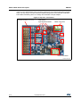
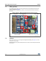
Figure 1 shows the top side of the EVAL-L9958 evaluation board.
Figure 1. EVAL-L9958 evaluation board - top side
The evaluation board size is 78 mm x 57 mm; the PCB is made by using FR4 glass epoxy
support with 2 copper layers.
The PCB and all components assembled in the evaluation board meet requirements of the
applicable RoHS directives.
1.2
Input connector and test point
The EVAL-L9958 needs a very limited number of signals: EN, DI, DIR and PWM. The
bidirectional communication with a microcontroller by the SPI interface allows the L9958
configuration, diagnosis and identification.
The SPI interface, the digital supply voltage(a) and the control signals are connected to the
microcontroller connector (4x18 pins, 0.1”).
The microcontroller connector (J8) is fully compatible with the SPC56 discovery boards(b).
a.
VDDIO, the supply voltage for SPI,
b.
SPD560P-DISP, SPC563M-DISP, SPC564A-DISP, SPC56L-Discovery
DocID027215 Rev 1
5/16
14
EVAL-L9958: Board description
UM1843
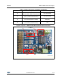
Thanks to the characteristic of this connector (male pins on top side and female on bottom
side), it is very easy to connect the EVAL-L9958 to the generic microcontroller evaluation
board without soldering wires or to design and assemble a simple adapter.
Figure 2. Top side – Connectors
&RQWUROOHU&RQQHFWRU - P D OH
7HVWSRLQWV
,QSXWVLJQDOVDQG63,
0RWRU&RQQHFWRU
3RZHU &RQQHFWRU
*$3*5,
6/16
DocID027215 Rev 1
UM1843
EVAL-L9958: Board description
Figure 3. Bottom side – Input Connector
-
&RQWUROOHU&RQQHFWRU
IHPDOH
*$3*5,
Table 1. Microcontroller connector (J8) – Pin description
Pin name
Description
A22
PWM input signal
C17
DI input signal
C18
DIR input signal
C26
SI input signal
D17
EN input signal
D18
CS - SPI
D25
SCK - SPI
D18
SO - SPI
C33
VDDIO
A34
GND
Two terminal blocs are used to connect the wires from the battery (DC source) and the
motor; the operating battery supply voltage is 4.0 ÷ 28 VDC.
DocID027215 Rev 1
7/16
14
EVAL-L9958: Board description
1.3
UM1843
LEDs and Rext
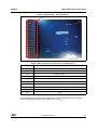
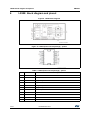
Four LEDs show the status of the VDD, Bat and the level of the signals DI and EN; their
position is depicted in Figure 4.
In the same figure is highlighted the position of the Rext (External Reference Resistor):
R4=10 kΩ.
Figure 4. Top side – LEDs and Rest Rext (external reference resistor)
/('9''
/('',DQG(1
/('9%DWW
9ROWDJHUHJXODWRU
1.4
5H[W([WHUQDOUHIHUHQFHUHVLVWRU
("1(3*
Jumpers
Many jumper allow to the user a large HW configuration flexibility (see Figure 5). In 1 the
description of each jumper.
Numerous jumpers are present allowing the user to monitor all control signal as well as the
SPI interface.
8/16
DocID027215 Rev 1
UM1843
EVAL-L9958: Board description
Table 2. Jumpers: description and default configuration
Jamper name
Descriptio
Default config
J2
DIR setting
(from uC, VDDIO, GND or external source)
2-3 (µController)
J3
EN Setting
(from uC, GND or external source)
1-2 (µController)
J4
VDD setting
(from internal regulator or VDDIO)
ON (+5V)
J6
VDD setting:
(from VDDIO or external source)
OFF
Figure 5. Top side – LEDs and Rest Rext (external reference resistor)
-
-DQG-
-
-
("1(3*
DocID027215 Rev 1
9/16
14
Schematic diagram
2
UM1843
Schematic diagram
Figure 6. EVAL-L9958 - Schematic diagram
10/16
DocID027215 Rev 1
UM1843
3
PCB layout
PCB layout
Figure 7. PCB Layout - Top side
Figure 8. PCB Layout - Bottom side
DocID027215 Rev 1
11/16
14
L9958: block diagram and pinout
4
UM1843
L9958: block diagram and pinout
Figure 9. L9958 block diagram
GAPG2411141518RI
Figure 10. L9958 (Power-SO 20 package) - pinout
Table 3. L9958 (Power-SO 20 package) - pinout
Pin
12/16
Pin Name
Description
1
GND
Ground
2
SO
Serial Out
3
VDDIO
Supply voltage SPI
4
CS
Chip Select
5
CP
Charge Pump
6
VS
Supply Voltage
7
DIR
Direction Input
8
OUT1
Output 1
9
DI
Disable
10
GND
Ground
11
GND
Ground
DocID027215 Rev 1
UM1843
L9958: block diagram and pinout
Table 3. L9958 (Power-SO 20 package) - pinout (continued)
Pin
Pin Name
Description
12
EN
Enable
13
OUT2
Output 2
14
PWM
PWM input
15
REXT
External Reference Resistor
16
SI
Serial In
17
SCK
Serial Clock
18
VDD
Supply Voltage
19
N.C.
Not Connected (To be connected toi GND on the PCB
20
GND
Ground
DocID027215 Rev 1
13/16
14
General handling precautions
Appendix A
UM1843
General handling precautions
The following precautions are recommended when using the EVAL-L9958 evaluation board:
14/16
•
Do not modify or manipulate the board and the device when the board is powered
and/or connected to the microcontroller or to a control board.
•
Do not supply the board with a DC source higher than the device maximum voltage
•
Any equipment or tool used for any manipulation of the semiconductor devices or
board modification should be connected to ground to avoid ESD.
•
The connectors and cables must be plugged and removed when the board is not
supplied.
•
Antistatic tools are recommended.
DocID027215 Rev 1
UM1843
Revision history
Revision history
Table 4. Document revision history
Date
Revision
25-Nov-2014
1
Changes
Initial release.
DocID027215 Rev 1
15/16
15
UM1843
IMPORTANT NOTICE – PLEASE READ CAREFULLY
STMicroelectronics NV and its subsidiaries (“ST”) reserve the right to make changes, corrections, enhancements, modifications, and
improvements to ST products and/or to this document at any time without notice. Purchasers should obtain the latest relevant information on
ST products before placing orders. ST products are sold pursuant to ST’s terms and conditions of sale in place at the time of order
acknowledgement.
Purchasers are solely responsible for the choice, selection, and use of ST products and ST assumes no liability for application assistance or
the design of Purchasers’ products.
No license, express or implied, to any intellectual property right is granted by ST herein.
Resale of ST products with provisions different from the information set forth herein shall void any warranty granted by ST for such product.
ST and the ST logo are trademarks of ST. All other product or service names are the property of their respective owners.
Information in this document supersedes and replaces information previously supplied in any prior versions of this document.
© 2014 STMicroelectronics – All rights reserved
16/16
DocID027215 Rev 1