1
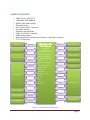
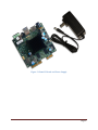
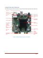
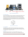
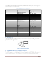
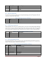
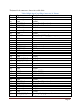
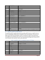
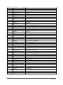
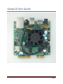
Gizmo II User Guide Page 1 Copyright © 2014, Gizmosphere. All rights reserved. DirectX, Microsoft and Windows are registered trademarks of Microsoft Corporation. OpenCL is a trademark of Apple, Inc. Linux is a registered trademark of Linus Torvalds. HDMI is a trademark of HDMI Licensing, LLC. PCIe is a registered trademark of PCI-SIG Corporation. Page 2 REVISION HISTORY Date September 2014 Revision 0.51 Description Preliminary release. Page 3 INTRODUCTION Gizmo II is the second generation open source x86 development board presented by GizmoSphere. Like the first Gizmo design, Gizmo II provides the power of a supercomputer and the I/O capabilities of a microcontroller. Built upon the award-winning AMD Embedded G-Series System-on-Chip (FT3), Gizmo II offers a high-performance, low-power affordable solution for a wide range of development projects. Gizmo II can be used in do-it-yourself (DIY) designs, embedded development, PC replacement, microcontroller applications, parallel processing, multicore engineering, and much more. The AMD Embedded G-Series SOC brings improvements to this newest offering in the line of Gizmo boards with the following benefits: Up to 113 percent improved CPU performance compared to the prior generation AMD Embedded G-Series APU. Support for DirectX® 11.1, OpenGL 4.2x and OpenCL™ 1.2, enabling parallel processing and high-performance graphics processing, and yielding up to a 20 percent graphics improvement over the previous AMD Embedded G-Series APU. Supported operating systems include Windows® Embedded 8 and Linux®. Suitable for a wealth of embedded applications including industrial control and automation, digital signage, electronic gaming systems, SMB storage, IP-TV, medical and network appliances, set-top boxes and more. Gizmo II comes with an updated list of peripheral interfaces including the much-requested and anticipated HDMI™ dedicated port, an mSATA port for connecting SSDs and a microSD card slot. In every significant manner, Gizmo II strives for greater flexibility and ease of use for embedded developers and DIY enthusiasts. Page 4 GIZMO II FEATURES • • • • • • • • • • • AMD G-Series SOC (FT3) 1GB DDR3-1600 SDRAM HDMI Video/Audio Output HD Audio In/Out mSATA/mini PCIe® Connector microSD Card Slot Onboard Gigabit Ethernet USB 3(2) and 2(2) Connectors AMD Debug Header High-speed and Low-speed Special Features Card Edge Connectors 4” x 4” Form Factor HDMI Conn PCIe® Gbit LAN Display Port0 PCIe X 1 (GPP1) PCIe X 1 (GPP0) AMD G-Series SOC FT3 Processor DDR3 Mem I/F DDR3-1600 2Gbx4 HD Audio I/F HD Audio Codec SD I/F microSD Card Slot SATA (1X) SATA Header (x1) SPI I/F SPI ROM 769 Ball BGA (0.8mm pitch) 24.5mmx24.5mm Package DDR3 (Single Channel) DirectX11 Integrated GP mPCIe/mSATA port LVDS/TMDS/HDMI/DP (x1) USB 2.0 (1X) VGA DAC PCIE Gen2 I/F (GFX 1x4) Display Port1 PCIE Gen2 I/F (GPP 4x1) Internal CLKGEN PCIe X 1 (GPP2) USB 2.0 (x8) USB 3.0 (x2) USB 2.0 (1X) SATA Gen 1/2/3 (x2) High Speed Conn PCIe X 1 (GPP3) HD Audio SD I/F SATA (1X) GPIO (8X) SPI I/F LPC I/F PWM (2X) Low Speed Conn Internal RTC USB 2.0 (2X) SPI I/F USB 2.0 ports (x2) USB 2.0 (2X) USB 3.0 ports (x2) USB 3.0 (2X) USB header USB 2.0 (1X) Counter (2X) JTAG EJTAG Header Figure 1 Gizmo II Block Diagram Page 5 Figure 2 Gizmo II Board and Power Supply Page 6 CONNECTORS AND INTERFACES The following figures show the locations of major Gizmo II board components and connections. Figure 3 Gizmo II Board Connector Locations Page 7 Figure 4 Gizmo II Board Back Panel J1 – DC Power Jack The Gizmo II board supports a wide range of input power specifications. Input voltage can range from 12V to 24V DC limited to 4A with a resettable fuse (F1). The included AC/DC power supply provides 12V@2A, 24W. Additional power (up to 24V@4A, 96W) may be required when using the Gizmo board with power-hungry USB or SATA devices and/or external boards connected to the high speed and/or low speed expansion ports. Power is connected to the Gizmo II board through the power jack J1. The center pin (Pin 1) carries the positive voltage input while the casing and shielding is ground. Figure 5 Power Jack J1 Pinout J2 – Dual USB3.0 Two USB3.0 ports are available from the Gizmo II board back panel. These connectors are colored blue to identify them as USB3.0. The top connector is connected to the SOC’s USB8 port while the bottom connector is connected to the SOC’s USB 9 port. The USB power pins are +5V fused through a 1A resettable PTC fuse (F5). J3 - HDMI The Gizmo II board’s primary display port is through the HDMI connector J3. (Note: Enable/Disable HDMI Audio Feature – Mount resistor R236 to enable HDMI Audio; mount Page 8 resistor R240 to disable HDMI Audio. Default is HDMI Audio enabled.) The connector pins are connected as shown in the table below: Pin 1 2 3 4 5 6 7 8 9 10 11 12 13 14 15 16 17 18 19 20 21 22 23 Table 1 HDMI Connector J3 Pinout Connector Pin Name Signal TMDS DATA2+ CON_DP0_TXDP TMDS DATA2 SHLD GND TMDS DATA2CON_DP0_TSDN TMDS DATA1+ CON_DP0_TX1P TMDS DATA1 SHLD GND TMDS DATA1CON_DP0_TX1N TMDS DATA0+ CON_DP0_TX2P TMDS DATA0 SHLD GND TMDS DATA0CON_DP0_TX2N TMDS CLK+ CON_DP0_TX3P TMDS CLK SHLD GND TMDS CLKCON_DP0_TX3N CEC HDMI_CEC RSVD N/C SCL CON_DP0_AUXP SDA CON_DP0_AUXN DCC/CEC GND GND +5V PWR Fused +5V (fuse F2 0.5A) HOT PLUG DTCT CON_DP0_HPD M1 GND M2 GND M3 GND M4 GND J4 – HD Audio I/O A RealTek HD Audio CODEC (ALC272) is connected to the audio jack J4. The pinout for the jack is shown in the figure below: Figure 6 Audio Jack J4 Pinout J5 – Combined USB2.0/RJ45 Ethernet Connector Two USB2.0 ports are available from the back panel along with an RJ45 Gigabit Ethernet port in a stack combined connector. The USB ports are colored black to distinguish them from the Page 9 USB3.0 ports, which are blue. The USB power pins are +5V fused through a 1A resettable PTC fuse (F4). The Ethernet port is controlled by a RealTek RTL8111EP Gigabit Ethernet Controller. J6 – USB2.0 Header An additional USB2.0 port is available through header J6. This header is connected to the SOC’s USB3 port. The pinout of this header is shown in the table below: Pin 1 2 3 4 5 Table 2 USB2.0 Header J6 Pinout Signal Fused +5V (resettable PTC fuse F6 0.5A) DataData+ GND N/C J8 – RCC Programming Header The Gizmo II board contains an STM8S003F3 8-bit microcontroller with EEPROM to handle power-up and reset states. This controller is accessible through the J8 programming header. (Note: Under most normal operations the programming of this microcontroller should not be modified. The header is not populated on the board to prevent users from erasing or reprogramming the device inadvertently, which will result in the board no longer functioning.) The pinout of this header is shown in the table below: Pin 1 2 3 4 Table 3 RCC Programming Header J8 Pinout Signal Description +3.3V_PROG 3.3V Board Power Rail SWIM Single Wire Interface Module for Programming GND Ground SWIM_RST Reset - refer to the STM8 SWIM communication protocol and debug module user manual (UM0470) J9 – SATA Data Connector By default this connector is not populated in the Gizmo II boards since an mSATA connector is available. The SATA interface on the AMD SOC supports port sharing, which means that multiple devices may be connected to the same SATA port. When populated, the J9 connector allows for a SATA device to be connected to the SOC SATA0 interface using a standard SATA cable. The pinout of the connector is shown in the table below: Pin 1 2 3 4 Signal GND SATA_TX0+ SATA_TX0GND Table 4 SATA Data Connector J9 Pinout Description Ground Transmit Positive Transmit Negative Ground Page 10 5 6 7 8 9 SATA_RX0SATA_RX0+ GND GND GND Receive Negative Receive Positive Ground Ground Ground J10 – APU Fan Connector The SOC Fan Connector provides power and speed monitoring to the fan. The pinout of the fan connector is shown in the table below: Pin 1 2 3 Signal GND FAN TACH Table 5 APU Fan Connector J10 Pinout Description Ground Fan Power Fan Speed J11 – SATA Power Connector When populated, the SATA power connector allows a low power (non-rotating media) SSD-type drive to receive its power from the Gizmo II board. The connector provides only a 5V supply for devices that require less than one amp. The pinout of the connector is shown in the table below: Pin 1 2 3 4 Signal +5V GND N/C N/C Table 6 SATA Power Connector Header J11 Pinout Description 5V Power Rail Ground No Connect No Connect J12 – SPI Programming Header The onboard SPI ROM can be programmed, read, and emulated through the SPI Programming Header. The header pinout is shown in the table below: Pin 1 2 3 4 5 6 7 8 Table 7 SPI Programming Header J12 Pinout Signal Description 3.3V SPI 3.3V SPI Power Rail GND Ground SPI_CS# SPI Device Chip Select SPI_CLK SPI Clock SPI_DATAIN SPI Data In SPI_DATAOUT SPI Data Out N/C No Connect N/C No Connect Page 11 J14 – MicroSD Card Socket The microSD card socket permits the Gizmo II board to read/write microSD card media. The Gizmo II board uses a G1745010 microSD Card Connector from Molex (http://www.molex.com/molex/products/family?key=microsd&channel=products&chanName=fa mily&pageTitle=Introduction). The connector pins are connected as shown in the table below: Pin 1 2 3 4 5 6 7 8 9A 9B 10A 10B Table 8 microSD Card Socket J14 Pinout Conn Pin Name Signal P9 SD_Data2 P1 SD_Data3 P2 SD_CMD P4 3.3V P5 SD_Clk P6 GND P7 SD_Data0 P8 SD_Data1 CD1 SD_CD# CD2 SD_CD# T1 GND T2 GND J15 – Low Speed Card Edge Connector The low speed card edge connector makes available several bus interfaces for developers to access in their prototype builds. The card edge connector is physically a PCIe 36-pin connector with a custom pinout. Figure 7 Low Speed Card Edge Connector (J15) The pinout is shown in the table below: Pin A1 A2 A3 A4 A5 A6 A7 A8 Table 9 Low Speed Card Edge Connector J15 Pinout Signal Description GEVENT0 General Purpose Event GPIO_0 General Purpose I/O GPIO_2 General Purpose I/O GPIO_4 General Purpose I/O PWM1(FANOUT1) FanOut 1 COUNTER1(FANIN1) FanIn 1 GND Ground PWM2(FANOUT2) FanOut2 Page 12 A9 A10 A11 A12 A13 A14 A15 A16 A17 A18 B1 B2 B3 B4 B5 B6 B7 B8 B9 B10 B11 B12 B13 B14 B15 B16 B17 B18 COUNTER2(FANIN2) GND SCL0 GND ADC0 ADC1 VDCIN (12V-24V) SYS_PBTN# USB0_DP USB0_DN GEVENT1# GPIO_1 GPIO_3 GPIO_5 GND SPI_CE SPI_CLK GND SPI_SO SPI_SI SDA0 GND DAC0 DAC1 +3.3V SYS_RST# GND GND FanIn 2 Ground Serial Clock Ground Analog/Digital Converter 0 Analog/Digital Converter 1 Fused Board Power (Resettable Fuse F7 0.5A) System Power Button USB Data+ (USB1 from SOC) USB Data- (USB1 from SOC) General Purpose Event1 General Purpose I/O General Purpose I/O General Purpose I/O Ground SPI Bus Chip Enable Serial Clock Ground SPI Bus Data Out SPI Bus Data In Serial Data Ground Digital/Analog Converter Digital/Analog Converter Fused +3.3V (Resettable PTC Fuse F8 0.5A) System Reset Signal Ground Ground J16 – High Speed Card Edge Connector The high speed card edge connector makes available several bus interfaces for developers to use in their prototype builds. The connector is physically identical to a PCIe x4 edge connector with custom pinout. Figure 8 High Speed Card Edge Connector J16 Page 13 The pinout for the connector is shown in the table below: Pin A1 A2 A3 A4 A5 A6 A7 A8 A9 A10 A11 A12 A13 A14 A15 A16 A17 A18 A19 A20 A21 A22 A23 A24 A25 A26 A27 A28 A29 A30 A31 A32 B1 B2 B3 B4 B5 B6 B7 B8 B9 Table 10 High Speed Card Edge Connector J16 Pinout Signal Description DP0_TX1_P Display Port 0 Transmitter 1+ DP0_TX1_N Display Port 0 Transmitter 1GND Ground DP0_TX3_P Display Port 0 Transmitter 3+ DP0_TX3_N Display Port 0 Transmitter 3GND Ground DP0_AUX_P Display Port 0 Aux+ DP0_AUX_N Display Port 0 AuxGND Ground DP0_HPD Display Port0 Hot Plug Detect +3.3V Fused 3.3V (Resettable PTC Fuse F9 1A) N/C No Connect N/C No Connect N/C No Connect +3.3V Fused 3.3V (Resettable PTC Fuse F9 1A) PCIE_RX0_P PCIe Receiver 0+ PCIE_RX0_N PCIe Receiver 0GND Ground PCIE_RX1_P PCIe Receiver 1+ PCIE_RX1_N PCIe Receiver 1GND Ground SATA_C_RX0_P SATA Receiver 0+ SATA_C_RX0_N SATA Receiver 0GND Ground N/C No Connect N/C No Connect GND Ground USBP1 USB 1+ (USB4) USBN1 USB 1- (USB4) USBP2 USB 2+ (USB5) USBN2 USB 2- (USB5) VIN_IN (12V-24V) Fused Board Input Voltage (Resettable PTC Fuse F3 1.1A) GND Ground DP0_TX0_P Display Port0 Transmitter 0+ DP0_TX0_N Display Port 0 Transmitter 0GND Ground DP0_TX2_P Display Port 0 Transmitter 2+ DP0_TX2_N Display Port 0 Transmitter 2GND Ground LVDS_VARY_BL Panel Backlight Brightness Control LVDS_DIGON Display Power Enable Page 14 B10 B11 B12 B13 B14 B15 B16 B17 B18 B19 B20 B21 B22 B23 B24 B25 B26 B27 B28 B29 B30 B31 B32 LVDS_BLON GND N/C N/C GND PCIE_TX0_P PCIE_TX0_N GND PCIE_TX1_P PCIE_TX1_N GND PCIE_CLK_P PCIE_CLK_N GND SATA_C_TX0_P SATA_C_TX0_N GND N/C N/C GND RESET GND VIN_IN (12V-24V) Backlight Enable Ground No Connect No Connect Ground PCIe Transmitter 0+ PCIe Transmitter 0Ground PCIe Transmitter 1+ PCIe Transmitter 1Ground PCIe Clock+ PCIe ClockGround SATA Transmitter 0+ SATA Transmitter 0Ground No Connect No Connect Ground System Reset Ground Fused Board Input Voltage (Resettable PTC Fuse F3 1.1A) J17 – miniPCIe/mSATA Combined Port The miniPCIe/mSATA combined port will accept either miniPCIe devices or mSATA devices and will automatically configure itself to the protocol of the connected device. This port can be used to connect SSD drives which have an mSATA connection or miniPCIe devices such as WIFI adapters. Non-compliant mSATA cards can be connected to this port, but mPCIe will have to be disabled first by removing resister R1 or by removing the gold finger pin43 on the mSATA card. The pinout of the connecter is shown in the table below: Pin 1 2 3 4 5 6 7 8 9 10 11 Table 11 miniPCIe/mSATA Combined Connector J17 Pinout Signal Description WAKE# PCIe Wakeup +3.3Vaux#2 Unfused 3.35V ALW COEX1 No Connect GND#4 Ground COEX2 No Connect 1.5V_1 Unfused 1.5V ALW CLKREQ# PCIe Mini CLK REQ UIM_PWR No Connect GND#9 Ground UIM_DATA No Connect REFCLKGPP CLK0Page 15 12 13 14 15 16 17 18 19 20 21 22 23 24 25 26 27 28 29 30 31 32 33 34 35 36 37 38 39 40 41 42 43 44 45 46 47 48 49 50 51 52 53 54 UIM_CLK REFCLK+ UIM_RESET GND#15 UIM_VPP UIM_C8 GND#18 UIM_C4 W_DISABLE# GND#21 PERST# PERn0 +3.3Vaux#24 PERp0 GND#26 GND#27 1.5V_2 GND#29 SMB_CLK PETn0 SMB_DATA PETp0 GND#34 GND#35 USB_DGND#37 USB_D+ +3.3Vaux#39 GND#40 +3.3Vaux#41 LED_WWAN# GND43 LED_WAN# RSV#45 LED_WPAN# RSV#47 1.5V_3 RSV#49 GND#50 RSV#51 +3.3Vaux#52 PAD#53 PAD#54 No Connect GPP CLK0+ No Connect Ground No Connect No Connect Ground No Connect WL Disable 0 Ground PCI Disable PCIe or SATA ReceiveUnfused 3.35V ALW PCIe or SATA Receive+ Ground Ground Unfused 1.5V ALW Ground Serial CLK (Sideband I/F) PCIe or SATA TransmitSerial DATA (Sideband I/F) PCIe or SATA Transmit+ Ground Ground USB2.0 (USB6) DataN Ground USB2.0 (USB6) DataP Unfused 3.35V ALW Ground Unfused 3.35V ALW Gizmo Board LED (D15) Control Output by Wireless LAN Ground Gizmo Board LED (D15) Control Output by Wireless LAN No Connect Gizmo Board LED (D15) Control Output by Wireless LAN No Connect Unfused 1.5V ALW No Connect Ground No Connect Unfused 3.35V ALW Ground Ground Page 16 COMPONENTS AMD G-Series SOC (FT3) The primary feature of the Gizmo II board is the AMD G-Series SOC (FT3). This processor is AMD’s first generation SOC design, which integrates Controller Hub functionality into the same package containing the CPU, Graphics Processor and North Bridge. The SOC on the Gizmo II board contain dual core Jaguar CPU cores with 2MB shared L2 cache. The embedded Graphics Processor provides support for DirectX 11.1 and realizes a significant compute performance (GFLOP) increase over the previous G-Series APUs. Two simultaneous displays are supported. On the Gizmo II board, one of these display outputs can be accessed through the HDMI connector. The other can be accessed on the High Speed Expansion card edge connector as a 4-lane DisplayPort 1.2, DVI, HDMI, or 18bpp single channel LVDS. The G-Series SOC has a single-channel DDR3 memory interface which supports DDR3-1600 devices. The Gizmo II comes with four 2Gb DDR3-1600 chips soldered down for a total of 1GB system memory. The board layout supports 4Gb chips which could provide up to 2GB of available memory. The controller hub functionality embedded into the G-Series SOC provides the following available interconnect: Four x1 links of PCIe Gen 2 for GPPs One x4 link of PCIe Gen 2 for discrete GPU Eight USB2.0 and 2 USB3.0 Two SATA 2.x/3.x (up to 6Gb/s) SD Card Reader v3.0 or SDIO controller Further information on the AMD Embedded G-Series SOC platform is available in the product brief and white paper. Audio CODEC (ALC272) The Realtek ALC272 is a High Definition Audio Codec, which features two stereo DACs, two stereo ADCs, legacy analog input to analog output mixing, one stereo digital microphone converter, and two independent SPDIF output converters. The ALC272 integrates two stereo ADCs and two stereo digital microphone converters to support simultaneous analog microphone recording and up to 4-channel digital microphone array recording, and features Acoustic Echo Cancellation (AEC), Beam Forming (BF), and Noise Suppression (NS) for voice applications. The HPOUT port is connected to the card edge audio jack and can drive a low noise signal to a connected audio input device or headphones. The same audio jack supports a MIC input which is connected to the ALC272 stereo microphone input port (the same signal is connected to both L and R). Page 17 For added flexibility, the ALC272 can be used to act as AD/DA converter for projects that require an analog input or output. There are two AD pins available on the low speed connector, which are connected to the audio codec’s line2 L and R inputs. The codec’s SURR L and R outputs are connected to the DA pins on the low speed connector and can be used as general purposed analog output. For more information on the Realtek Audio Codec or to download drivers, visit the Realtek Audio Codec website. Gigabit Ethernet Controller The Realtek RTL8111 Gigabit Ethernet controller combines a triple-speed IEEE 802.3 compliant Media Access Controller (MAC) with a triple-speed Ethernet transceiver, PCI Express bus controller, and embedded memory. With state-of-the-art DSP technology and mixed-mode signal technology, it offers high-speed transmission over CAT 5 UTP cable or CAT 3 UTP (10Mbps only) cable. Functions such as Crossover Detection & Auto-Correction, polarity correction, adaptive equalization, cross-talk cancellation, echo cancellation, timing recovery, and error correction are implemented to provide robust transmission and reception capability at high speeds. The device supports the PCI Express 1.0a bus interface for host communications with power management and is compliant with the IEEE 802.3u specification for 10/100Mbps Ethernet and the IEEE 802.3ab specification for 1000Mbps Ethernet. It also supports an auxiliary power autodetect function, and will auto-configure related bits of the PCI power management registers in PCI configuration space. The Ethernet controller device is physically connected to the PCIe x1 GPP Port 1. The Ethernet port of the RTL8111 is connected to the RJ45 jack on the Gizmo II’s back panel. SPI ROM The Gizmo II board contains a MX25L3239E 32Mb SPI ROM which is preloaded with the SageBIOS BSP (Board Support Package). This is a full boot solution with minimal footprint that is based on the open source coreboot project. The ROM can be reprogrammed through the SPI programming header J12. mSATA/miniPCIe Connector The mSATA/miniPCIe connector located on the bottom side of the board can be used for SATA 2.x/3.x (up to 6Gb/s) storage devices. DDR3 Memory There are four 2Gb x 16 DDR3-1600 components soldered to the Gizmo II board. These are connected to the single channel DDR3 memory port on the AMD SOC. The address connections on the PCB will support device sizes up to 4Gb, which would give a maximum RAM capacity of 2GB. This is a manufacturing option only. It is not recommended that users attempt to remove or resolder the BGA memory components. Power Button The Power button initiates the power-up sequence. Press once to power up the board. Press and hold to power down the board. Page 18 Reset Button Pressing the Reset button causes a hard reset of the board. RTC Battery (backside) The 3V coin battery (included) provides power for the realtime clock (RTC). The battery must be installed for proper operation of the board. GIZMO II SWITCH, LED, HEADER, AND TEST POINT LIST Table 12 Diodes, Switches, Connectors and Headers Item Function GPIO SW1 Power Button SW2 Reset Button D12 Red LED – SD Card Activity 45 D24 Green LED – IR Activity 184 D15 Red LED – Wireless Activity D6 Red LED – DASH RCC SYS Alert D1 Red LED – Standby Power D3 Red LED – S5 Power Indicator D4 Green LED – SATA Activity J1 Power Jack J2 Dual USB3 Connectors J3 HDMI Connector J4 Audio Jack J5 Dual USB2/RJ45 Connector J6 USB2 Port 3 Header J8 RCC Programming Header J9 SATA0 Connector J10 APU Fan Header J11 SATA Power Connector (5V only) J12 SPI ROM Programming Header J13 AMD Debug Header Page 19 Table 13 Gizmo II Board Test Points Item TP1 TP2 TP3 TP4 TP5 TP6 TP7 TP8 TP9 TP10 TP13 TP14 TP15 TP16 TP17 TP18 TP19 TP20 TP21 TP22 TP23 TP24 TP25 TP26 TP27 TP28 TP29 TP30 TP31 TP32 TP33 TP34 TP36 TP37 Function SATA_X1 SATA_X2 SD_WP SD_PWR_CNTL APU_TEST16 APU_TEST17 APU_TEST14 APU_TEST15 APU_TEST34 USBCLK14M_CLK TEST2 TEST1/TMS USB_OC# APU_TEST43 – USB_ATEST1 APU_TEST42 – USB_ATEST0 48M_CLK TEST0 DAC_SCL DAC_VSYNC DAC_SDA AP_TEST36 APU_TEST6 APU_TEST37 APU_TEST4 APU_TEST5 APU_TEST41 – TMON_CAL APU_TEST40 – M_ANALOGOUT APU_TEST39 – M_ANALOGIN APU_TEST31 APU_TEST28_L APU_TEST28_H M_VREFDQ GPIO55 GPIO69 GPIO 55 69 Page 20