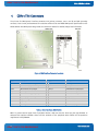
1
DRAFT COPY FOR REVIEW ONLY >> Kontron User’s Guide << COMe-cTH6 Document Revision 0.83 DRAFT COPY FOR REVIEW ONLY www.kontron.com DRAFT COPY FOR REVIEW ONLY DRAFT COPY FOR REVIEW ONLY DRAFT COPY FOR REVIEW ONLY COMe-cTH6 User’s Guide >> Table of Contents << 1 User Information ............................................................................1 1.1 About This Document ............................................................................................................... 1 1.2 Copyright Notice ..................................................................................................................... 1 1.3 Trademarks ............................................................................................................................ 1 1.4 Standards ............................................................................................................................. 1 1.5 Warranty ............................................................................................................................... 2 1.6 Technical Support ................................................................................................................... 2 2 Introduction ..................................................................................3 2.1 The COMe-cTH6 Module ............................................................................................................ 3 2.2 Naming Clarifications............................................................................................................... 3 2.3 Understanding the COM Functionality .......................................................................................... 4 2.4 COM Express® Documentation ................................................................................................... 5 2.5 COM Express® Module Benefits .................................................................................................. 5 3 Specifications ................................................................................6 3.1 Functional Specification ........................................................................................................... 6 3.1.4 Processor: AMD R-Series Fusion Accelerated Processing Unit (APU)................................................... 6 3.1.5 Chipset: AMD Fusion Controller Hub (FCH) ................................................................................... 6 3.1.6 Onboard Devices: ................................................................................................................... 7 3.1.7 Additional Interfaces: ............................................................................................................. 7 3.2 Functional Block Diagram ......................................................................................................... 8 3.3 Mechanical Specifications ......................................................................................................... 9 3.3.1 Module Dimensions ................................................................................................................ 9 3.3.2 Height on Top ....................................................................................................................... 9 3.3.3 Height on Bottom .................................................................................................................. 9 3.4 Electrical Specifications ......................................................................................................... 10 3.5 ATX Power ........................................................................................................................... 10 3.5.1 Single Power Supply ............................................................................................................. 10 3.5.2 Supply Current (Windows) ..................................................................................................... 10 3.6 i Environmental Specifications .................................................................................................. 11 DRAFT COPY FOR REVIEW ONLY www.kontron.com DRAFT COPY FOR REVIEW ONLY COMe-cTH6 User’s Guide 3.6.1 Temperature ....................................................................................................................... 11 3.6.2 Operating: (with Kontron heat spreader plate assembly): ............................................................. 11 3.6.3 Operating: ......................................................................................................................... 11 3.6.4 Humidity ........................................................................................................................... 11 3.7 MTBF .................................................................................................................................. 11 4 COMe-cTH6 Connectors ................................................................... 12 4.1 Pin-Outs ............................................................................................................................. 13 4.1.1 Connectors X1A and X1B: COM Express® Interface (Type 6) ........................................................... 13 4.1.2 Connector J1 – Fan .............................................................................................................. 23 4.1.3 Connectors J2 and J3 – SO-DIMM DDR3 Memory Sockets ............................................................... 23 4.1.4 Connector J4 – JTAG (AMD Embedded Probe) ............................................................................. 24 5 COMe-cTH6 Interfaces .................................................................... 25 5.1 PCI Express Interface ............................................................................................................. 25 5.2 USB Interface....................................................................................................................... 25 5.2.1 USB 2.0 Interface ................................................................................................................ 25 5.2.2 USB 3.0 Interface ................................................................................................................ 25 5.2.3 Configuration ..................................................................................................................... 26 5.3 5.3.1 5.4 5.4.1 5.5 5.5.1 5.6 SATA Interface ..................................................................................................................... 27 Configuration ..................................................................................................................... 27 Audio Interface .................................................................................................................... 27 Configuration ..................................................................................................................... 27 LPC Serial IRQ ...................................................................................................................... 27 Configuration ..................................................................................................................... 27 Graphics Interface ................................................................................................................. 28 5.6.1 Analog VGA ........................................................................................................................ 28 5.6.2 LVDS Flat Panel Interface ....................................................................................................... 28 5.7 5.7.1 Ethernet Interface................................................................................................................. 28 Configuration ..................................................................................................................... 28 5.8 SPI Bus Interface .................................................................................................................. 29 5.9 LPC Bus Interface .................................................................................................................. 29 ii DRAFT COPY FOR REVIEW ONLY www.kontron.com DRAFT COPY FOR REVIEW ONLY 5.10 COMe-cTH6 User’s Guide Power Control Interface .......................................................................................................... 30 5.10.1 Power Good (PWR_OK) .......................................................................................................... 30 5.10.2 Power Button (PWRBTN#) ...................................................................................................... 30 5.10.3 5.10.3 Reset Button (SYS_RESET#) .......................................................................................... 30 5.11 Power Supply ....................................................................................................................... 31 5.11.1 ATX Mode / Single Supply Mode .............................................................................................. 31 5.12 Miscellaneous Circuits ............................................................................................................ 32 5.12.1 Speaker ............................................................................................................................. 32 5.12.2 Battery .............................................................................................................................. 32 5.12.3 I2C Bus .............................................................................................................................. 32 5.12.4 SMBus ............................................................................................................................... 32 6 Special Features............................................................................ 33 6.1 Watchdog Timer (WDT) ........................................................................................................... 33 6.2 General Purpose Input and Output (GPIO) .................................................................................. 33 6.3 ACPI Suspend Modes and Resume Events .................................................................................... 34 6.3.1 Events that Resume the System from S3/S4 ............................................................................... 34 6.3.2 Events that Resume the System from S5 .................................................................................... 34 6.3.3 Events that Resume the System from S5 Eco ............................................................................... 34 7 Design Considerations .................................................................... 35 7.1 Thermal Management ............................................................................................................ 35 7.2 Heat Spreader Dimensions ...................................................................................................... 35 7.3 Onboard Fan Connector .......................................................................................................... 36 7.3.1 Fan Connector Electrical Characteristics .................................................................................... 37 8 System Resources .......................................................................... 38 8.1 Interrupt Request (IRQ) Lines .................................................................................................. 38 8.2 Memory Area ........................................................................................................................ 38 8.3 I/O Address Map ................................................................................................................... 38 8.4 Peripheral Component Interconnect (PCI) Devices ........................................................................ 39 8.5 System Management Bus (SMBus) ............................................................................................ 40 9 BIOS Operation ............................................................................. 41 iii DRAFT COPY FOR REVIEW ONLY www.kontron.com DRAFT COPY FOR REVIEW ONLY COMe-cTH6 User’s Guide 9.1 Determining the BIOS Version .................................................................................................. 41 9.2 BIOS Setup Guide .................................................................................................................. 41 9.3 BIOS Setup Options ............................................................................................................... 43 9.3.1 Main Menu ......................................................................................................................... 43 9.3.2 Advanced Menu ................................................................................................................... 45 9.3.3 Chipset .............................................................................................................................. 62 9.3.4 Boot Configuration .............................................................................................................. 70 9.3.5 Security ............................................................................................................................. 72 9.3.6 Save and Exit ...................................................................................................................... 73 Appendix A: Architecture Information ...................................................... 74 Document Revision History .................................................................... 76 iv DRAFT COPY FOR REVIEW ONLY www.kontron.com DRAFT COPY FOR REVIEW ONLY 1 1.1 COMe-cTH6 User’s Guide User Information About This Document This document provides information about products from Kontron and/or its subsidiaries. No warranty of suitability, purpose, or fitness is implied. While every attempt has been made to ensure that the information in this document is accurate, the information contained within is supplied “as-is” and is subject to change without notice. For the circuits, descriptions and tables indicated, Kontron assumes no responsibility as far as patents or other rights of third parties are concerned. 1.2 Copyright Notice Copyright © 2013 Kontron America Inc. All rights reserved. No part of this document may be reproduced, transmitted, transcribed, stored in a retrieval system, or translated into any language or computer language, in any form or by any means (electronic, mechanical, photocopying, recording, or otherwise), without the express written permission of Kontron. ETX®, ETXexpress® and microETXexpress® are trademarks or registered trademarks of Kontron Europe GmbH. Kontron is a trademark or registered trademark of Kontron AG. 1.3 Trademarks The following components used on this board are trademarked as follows: » IBM, XT, AT, PS/2 and Personal System/2 are trademarks of International Business Machines Corporation. » Microsoft is a registered trademark of Microsoft Corporation. » Intel is a registered trademark of Intel Corporation. » COM Express is a trademark of PICMG. » All other products and trademarks mentioned in this manual are trademarks of their respective owners and indicated with an “*”. 1.4 Standards Kontron America Inc. is certified to ISO 9001-2008 and ISO 13485-2003 standards. 1 DRAFT COPY FOR REVIEW ONLY www.kontron.com DRAFT COPY FOR REVIEW ONLY 1.5 COMe-cTH6 User’s Guide Warranty This Kontron product is warranted against defects in material and workmanship for the warranty period from the date of shipment. During the warranty period, Kontron will, at its discretion, decide to repair or replace defective products. Within the warranty period, the repair of products is free of charge as long as warranty conditions are observed. The warranty does not apply to defects resulting from improper or inadequate maintenance or handling by the buyer, unauthorized modification or misuse, operation outside of the product’s environmental specifications or improper installation or maintenance. Kontron is not responsible for any defects or damages to other products not supplied by Kontron that are caused by a faulty Kontron product. 1.6 Technical Support Technicians and engineers from Kontron and/or its subsidiaries are available for technical support. We are committed to making our product easy to use and will help you use our products in your systems. Please consult our website at http://www.kontron.com/support for the latest product documentation, utilities, drivers and support contacts. Consult our customer section for the latest BIOS downloads, Product Change Notifications and additional tools and software. You can also always contact your board supplier for technical support. 2 DRAFT COPY FOR REVIEW ONLY www.kontron.com DRAFT COPY FOR REVIEW ONLY 2 2.1 COMe-cTH6 User’s Guide Introduction The COMe-cTH6 Module The Kontron COMe-cTH6 COM module complies with the Rev. 2.0 COM Express® specification that provides for a compact form factor (95 x 95 mm) and new COM Express® Type 6 connector definitions. The COMe-cTH6 module design enables the development of graphics-intensive applications based on the Advanced Micro Devices (AMD) RSeries Advanced Processing Unit (APU) and the AMD M3 Fusion Controller Hub (FCH) using the secure development path of an established, future-proof industry standard, the COM Express® compact form factor and pin-out Type 6. The AMD processor on the Kontron COMe-cTH6 module has two integrated memory controllers for up to 8 GBytes (2x4GB) per channel of DDR3 memory. Support for the latest 3D graphics is provided by the integrated Radeon TM graphics controller which also provides four independent display interfaces supported with daisy chaining and a maximum resolution of 2560 x 1600 x 60 Hz (Display Port) or 1920 x 1200 x 60 Hz (HDMI/DVI). With seven PCI Express x1 lanes and 8 PEG lanes for flexible configurations, the COMe-cTH6 module is ideal for multi-interface designs and brings the added benefit of low power consumption. These special features make this 95 x 95 mm compact Computer-on-Module a key solution for applications such as multimedia content delivery, outdoor digital signage, infotainment kiosks, POS/POI devices, panel PCs, and professional gaming systems that require high-level graphics performance and support for the latest APIs like DirectX 11, and where low thermal power design is also an advantage. All modules in the Kontron COM Express® family are compliant with the COM Express® standard. These modules also take advantage of the Kontron Embedded Application Programming Interface (Kontron EAPI), which is cross-platform middleware that is both form factor and operating system independent. This ensures easy interchangeability as well as design scalability and future migration paths. The COMe-cTH6 module is a complete PC with standard interfaces such as USB 2.0 and USB 3.0, Gigabit Ethernet, SATA 3.0, as well as additional features like high-definition audio (HDA) and ACPI 3.0, Fast I2C, SPI, LPC, RTC, 2x serial ports (RX, TX) and S5 Eco. 2.2 Naming Clarifications The COM Express® standard defines a Computer-On-Module, or COM, with all the components necessary for a bootable host computer, packaged as a super-component. The interfaces provide a smooth transition path from legacy parallel interfaces such as IDE or parallel ATA (PATA) to Low Voltage Differential Signaling (LVDS) interfaces including PCI Express* and Serial ATA (SATA). » Basic COM Express® modules have a 125mm x 95mm form factor and follow pin-out types 2 or 6. » Compact COM Express® modules have a 95mm x 95mm form factor and follow pin-out types 2 or 6. » Mini COM Express® modules have a 55mm x 84mm form factor and follow pin-out types 1 or 10. NOTE: The Kontron COMe-cTH6 compact module takes advantage of new features introduced in the PICMG R2.0 COM Express® Specification. 3 DRAFT COPY FOR REVIEW ONLY www.kontron.com DRAFT COPY FOR REVIEW ONLY 2.3 COMe-cTH6 User’s Guide Understanding the COM Functionality All Kontron COM Express® modules contain two COM Express connectors (X1A and X1B), each with two rows. The primary connector rows are Row A and Row B (connector X1A). The secondary connector rows are Row C and Row D (connector X1B). The COMe-cTH6 module uses the PICMG COM Express® pin-out Type 6 definition, which is a recent addition to the PICMG COM Express standard and documented in Revision 2.0 of the PICMG specification. The Type 6 pin-out is based on Type 2 and also supports new features on the secondary connector. The key changes are: » The PCI interface is no longer supported and the pins are used instead for digital display interfaces (DDI) and two additional PCI Express lanes » The IDE (PATA) parallel interface is no longer supported and the pins are used instead for additional transmit and receive pairs for four USB 3.0 ports. » Three dedicated DDI ports have been added. Ports 1, 2, and 3 can be configured individually for Display Port (DP), HDMI, or DVI and port 1 can also be used for SDV0. » Two optional two-wire RS232 serial ports have been added using pins formerly assigned to 12V signals. The primary connector (Row A and Row B) on the COMe-cTH6 module features the following functionality: » Analog VGA graphics » Gigabit Ethernet LAN » Serial ATA (SATA) » PCI Express* » USB 2.0 and USB 3.0 » Express card » Wake » Speaker » Intel® High Definition Audio (HDA) » LPC (Low Pin Count) bus » TTL serial » Watchdog timer (WDT) » GPIO » I2C » Power button » SPI (Serial Peripheral Interface) Bus The secondary connector (Row C and Row D) supports the following buses and I/O: » PEG x16 (the COMe-cTH6 is limited to 8 lanes, either the upper 8 or lower 8) » PCI Express » DDI » DP/DVI/HDMI » LVDS 18/24-bit single/dual channel NOTE: For full descriptions of the COM Express Type 6 pin-outs, refer to the PICMG documentation. 4 DRAFT COPY FOR REVIEW ONLY www.kontron.com DRAFT COPY FOR REVIEW ONLY 2.4 COMe-cTH6 User’s Guide COM Express® Documentation This product manual serves as one of three principal references for this COM Express® module design. It documents the specifications and features of the COMe-cTH6 module. The other two references, which are available from your Kontron support representative or from PICMG, include: » The PICMG COM.0 COM Express® Module Base Specification, Revision 2.0, which defines the COM Express® module form factors, pin-outs, and signals. This document can be obtained by filling out the order form on the PIGMG website at http://www.picmg.com . » The PICMG COM Express® Design Guide, which serves as a general guide for baseboard design, with a focus on maximum flexibility to accommodate a wide range of COM Express® modules. This guide is on the PICMG website at http://www.picmg.com. 2.5 COM Express® Module Benefits Compact form factor (95 x 95 mm) Computer-on-Module Express (COM Express) modules are very compact, highly integrated computers that use either the Type 2 or Type 6 COM Express® connector pin-outs. All compact COM Express modules feature a standardized form factor and a standardized connector layout for a specified set of signals, as defined in the PICMG COM Express® specification (PICMG COM.0.R2). This standardization lets designers create a single-system baseboard that can accept present and future COM Express modules. Kontron COM Express® modules include common personal computer (PC) peripheral functions such as: » Graphics » USB ports » Ethernet » Audio » SATA hard disk drive format Baseboard designers can optimize exactly how each of these functions is implemented physically for the intended application by placing connectors precisely where they are needed on a baseboard that is designed for an optimal fit in the system packaging. A peripheral PCI Express bus can be implemented directly on the application-specific baseboard rather than on mechanically unwieldy expansion cards. The ability to build a system on a single baseboard using the computer as one plug-in super-component simplifies packaging, eliminates cabling, and significantly reduces system-level total cost of ownership. A single baseboard design can use a range of COM Express modules. This flexibility enables product differentiation at various price/performance points, and the design of future-proof systems with a built-in upgrade path. The modularity of a COM Express solution also ensures against obsolescence as computer technology evolves. A properly designed COM Express baseboard can work with several successive generations of COM Express modules. A COM Express baseboard design has many of the advantages of a custom, computer-board design, but delivers better obsolescence protection, greatly reduced engineering effort, and faster time to market. 5 DRAFT COPY FOR REVIEW ONLY www.kontron.com DRAFT COPY FOR REVIEW ONLY 3 3.1 COMe-cTH6 User’s Guide Specifications Functional Specification 3.1.4 Processor: AMD R-Series Fusion Accelerated Processing Unit (APU) » CPU: AMD R-460L quad core 2.0 (2.8) GHz (25W) AMD R-452L quad core 1.6 (2.4) GHz (19W) AMD R-260H dual core 2.1 (2.6) GHz (17W) » Cores: Up to four cores » Processor Speed: Up to 4x 2.8 GHz » Memory Controller: Up to 16 GBytes (2x8GB) DDR3 (1066/1333 MT/s) » Graphics Interfaces: Integrated AMD Radeon™ HD 7000 series graphics controller Enhanced DirectX®11 graphics multimedia support HD decode for H.264, VC-1, MPEG-2, DivX HW encode for H.264 at 1080p@60fps PEG x8, software-configurable as x1, x2, x4, and x8 Dual channel (18/24-bit) LVDS via Analogix ANX3110 DP-to-LVDS translator » Display Support: Four displays with AMD Eyefinity technology (two non-DP plus DP or VGA) 3x DDI interfaces(HDMI/DVI/Display Port) including 1x eDP Additional 3x DP interfaces (multiplexed with PEG) Display Port resolution up to 2560 x 1600 x 60 Hx HDMI/DVI resolution up to 1920 x 1200 x 60 Hz Single analog VGA resolution up to 1960 x 1600 x 60Hz 1x CRT » I/O Interfaces PCI Express 2.0: four PCIe general purpose lanes (Gen 1 and Gen 2) configurable as x1, x2, and x4 » Instruction Set: Kontron Embedded Application Programming Interface (Kontron EAPI) » Package: 27mm x 31mm » Thermal Spec: Operation: 0° to +60°C Storage: -40° to +85° 3.1.5 Chipset: AMD Fusion Controller Hub (FCH) » FCH AMD A70M M3 Fusion Controller Hub » Storage 4x SATA 3.0 with 6 Gbits/sec maximum transfer rate » PCI Express: three PCIe general purpose x1 Gen 2 lanes () software-configurable as x3, or as 1 x2 and 1 x1Express Card: Control signals for two Express Cards Audio: three HDA audio channels mapped to COM Express AC/HDA, Speaker Out USB 2.0: eight ports mapped to two EHCI controllers (5 to one EHCI and 3 to another) USB 3.0: four Super Speed ports » LPC LPC bus brought to COM Express connector » TPM Atmel AT97SC3204 TPM 6 DRAFT COPY FOR REVIEW ONLY www.kontron.com DRAFT COPY FOR REVIEW ONLY COMe-cTH6 User’s Guide » Watchdog Timer WDT via CPLD » GPIO Four GPIs and four GPOs available on the COM Express connector » SMBus SMBus brought to the COM Express connector via FCH » I2C I2C master with 7-bit I2C addressing with 100 KHz or 400 KHz operation and controller on CPLD, for off- and on- module use » External BIOS ROM Support for carrier board SPI devices (new with COM Express Rev 2) » Suspend Modes Core Sleep States: S0, S3, S4, S5, S5 Eco » Wake WAKE0#, WAKE1# support » TDP: 2.3W » Package: 24.5mmx24.5mm 3.1.6 Onboard Devices: » Ethernet: Intel® I210-AT GbE Controller 10/100/1000 Mbit » LVDS Analogix ANX3110 18/24-bit single/dual channel DP/LVDS Translator » CPLD Altera EPM1270 CPLD » Watchdog Timer: BIOS enables and configures watchdog in the CPLD » Hardware Monitor Nuvoton NCT7904D chip » I C EEPROM AT24HC04B serial EEPROM for module parameter storage » TPM Trusted Platform Module uses Atmel AT97SC3204 chip » Fan Header Molex 53261-0371 3-pin header for consistency with Kontron Universal Cooling Solution » Power Management: BIOS-enabled ACPI 4.0 power management for supported OSs 2 3.1.7 Additional Interfaces: » Passive Cooling: Passive and Critical Trip Point » ACPI: ACPI 4.0 » Input Voltage: Single supply support with wide range 5.0V supply is the optional standby power rail. 7 DRAFT COPY FOR REVIEW ONLY power supply input, 4.75V – 20V www.kontron.com DRAFT COPY FOR REVIEW ONLY 3.2 COMe-cTH6 User’s Guide Functional Block Diagram Figure 1 is the COMe-cTH6 COM Express™ Type 6 module block diagram. Figure 1: COMe-cTH6 COM (Type 6) Block Diagram 8 DRAFT COPY FOR REVIEW ONLY www.kontron.com DRAFT COPY FOR REVIEW ONLY 3.3 COMe-cTH6 User’s Guide Mechanical Specifications 3.3.1 Module Dimensions » 95 mm x 95 mm ±0.2 mm (3.47 in. x 3.47 in) 3.3.2 Height on Top » Approximately 8.0 mm maximum (without the PCB) » Height varies depending on whether an optional cooling solution (either a passive heat sink or a heat spreader plate) is installed 3.3.3 Height on Bottom » Approximately 4.06 mm maximum (without the PCB) Figure 2: COMe-cTH6 Module Mechanical Drawing All dimensions are shown in millimeters. The COM Express® specification says that these holes should be ± 0.25mm [±0.010"], unless otherwise noted. The tolerances for placement of the COM Express connector with respect to the peg holes (dimensions [16.50, 6.00]) should be ± 0.10mm [±0.004"]. The mounting holes shown in the drawing use 6mm diameter pads and 2.7mm plated holes for use with 2.5mm hardware. The pads are tied to the PCB ground plane. Black circles represent the mounting holes required by the PICMG COM Express® standard. 9 DRAFT COPY FOR REVIEW ONLY www.kontron.com DRAFT COPY FOR REVIEW ONLY 3.4 Electrical Specifications 3.5 ATX Power COMe-cTH6 User’s Guide Main power is on the COM Express VCC_12V pins and standby power is on the VCC_5V_SBY pins. RTC power is provided on the VCC_RTC pins. VCC_12V may or may not collapse in suspend states S3, S4, and S5. 3.5.1 Single Power Supply 4.75V to +20V main power is on the COM Express VCC_12V pins and standby power, if needed, is also provided on the VCC_12V pins. The VCC_5V_SBY pins may be floating or may be tied to a 5V source on the carrier board. RTC power is provided on the VCC_RTC pins. 3.5.2 Supply Current (Windows) The testing performed to capture the supply current data used tested modules mounted on a Kontron evaluation board with a mouse and keyboard connected. The power consumption tests were executed in Windows XP (with SP3) using a tool to stress the CPU at 100 % load. The power measurement values were captured after 15 minutes of full load or a stable CPU core temperature of 90°C. To ensure a stable die temperature, a corresponding heat sink was used to hold the temperature under the critical trip point. The modules were tested using the maximum CPU frequency. For more detailed information, refer to the “Power Consumption” diagrams on the EMD Customer section of the Kontron website. Module Power Consumption by Main 4.75V 12V 20V Windows Desktop (idle) 5.0W 5.6W 6.0W TAT at maximum power configuration 33.8W 34.4W 35.0W S3 with Wake-on-LAN disabled 0.7W 0.8W 0.9W S5 with Wake-on-LAN disabled 0.4W 0.5W 0.6W ~0.005W 0.02W 0.05W Input Supply Voltage S5 Eco NOTE: It is impossible to test for all possible applications on the market. There may be an application that draws more power from the CPU than the values measured in the table above. Take this into consideration if you are at the limit of the thermal specification, in which case you should consider improving your thermal solution. 10 DRAFT COPY FOR REVIEW ONLY www.kontron.com DRAFT COPY FOR REVIEW ONLY 3.6 COMe-cTH6 User’s Guide Environmental Specifications 3.6.1 Temperature 3.6.2 Operating: (with Kontron heat spreader plate assembly): » Ambient temperature: 0 to 60°C with an active fan heat sink. » Non-operating: -30 to +85°C NOTE: The maximum operating temperature with the heat spreader plate installed is the maximum measurable temperature on any spot on the heat spreader surface. You must maintain the temperature according to the specification above. 3.6.3 Operating: » Maximum operating temperature: 0-60°C » Non operating: -30°C to +85°C NOTE: The maximum operating temperature is the maximum measurable temperature on any spot on the module surface. You must maintain the temperature according to the specification above. 3.6.4 Humidity » Operating: 10% to 90%, non-condensing » Non operating: 5% to 95%, non-condensing 3.7 MTBF TBD 11 DRAFT COPY FOR REVIEW ONLY www.kontron.com DRAFT COPY FOR REVIEW ONLY 4 COMe-cTH6 User’s Guide COMe-cTH6 Connectors The pin-outs for COM Express® interface connectors X1A (primary connector, rows A and B) and X1B (secondary connector, rows C and D) are documented for convenient reference. See the PICMG COM Express® Specification on the PICMG website and COM Express® Design Guide on the Kontron website for detailed, design-level information. Figure 3: COM Interface Connector Locations Type Description Type Description I/O-3.3 Bi-directional 3.3 V IO-Signal O-3,3 3.3V Output I/O-5T Bi-dir. 3.3V I/O (5V Tolerance) O-5 5V Output I/O-5 Bi-directional 5V I/O-Signal DP-I/O Differential Pair Input/Output I-3,3 3.3V Input DP-I Differential Pair Input I/OD Bi-directional Input/Output Open Drain DP-O Differential Pair Output I-5T 3.3V Input (5V Tolerance) PU Pull-Up Resistor OA Output Analog PD Pull-Down Resistor OD Output Open Drain PWR Power Connection O-1,8 1.8V Output nc Not connected, Signal not available Table 1: Electrical Signal Abbreviation NOTE: To protect external power lines of peripheral devices, make sure that the wires have the right diameter to withstand the maximum available current and the enclosure of the peripheral device fulfills the fire-protection requirements in IEC/EN60950. 12 DRAFT COPY FOR REVIEW ONLY www.kontron.com DRAFT COPY FOR REVIEW ONLY 4.1 COMe-cTH6 User’s Guide Pin-Outs 4.1.1 Connectors X1A and X1B: COM Express® Interface (Type 6) NOTE: The termination resistors in these tables are already mounted on the COMe-cTH6 module. Refer to the PICMG COM Express® Design Guide for information about additional termination resistors Pin Signal Description Type Termination Comment A1 GND1 Power Ground PWR - - A2 GBE0_MDI3- Ethernet Receive Data- DP-I Intel® I210-AT - A3 GBE0_MDI3+ Ethernet Receive Data+ DP-I Intel® I210-AT - A4 GBE0_LINK100 Ethernet Speed LED 100Mbps OD A5 GBE0_LINK1000 Ethernet Speed LED 1000Mbps OD A6 GBE0_MDI2- Ethernet Receive Data- DP-I Intel® I210-AT - A7 GBE0_MDI2+ Ethernet Receive Data+ DP-I Intel® I210-AT - A8 GBE0_LINK LAN Link LED OD A9 GBE0_MDI1- Ethernet Receive Data- DP-I Intel® I210-AT - A10 GBE0_MDI1+ Ethernet Receive Data+ DP-I Intel® I210-AT - A11 GND2 (Fixed) Power Ground PWR - - A12 GBE0_MDI0- Ethernet Transmit Data- DP-O Intel® I210-AT - A13 GBE0_MDI0+ Ethernet Transmit Data+ DP-O Intel® I210-AT - A14 GBE0_CTREF LAN Reference Voltage O-3.3 A15 SUS_S3 Indicates Suspend to RAM state O-3.3 A16 SATA0_TX+ SATA 0 Transmit Data+ DP-O - A17 SATA0_TX- SATA 0 Transmit Data- DP-O - A18 SUS_S4 Indicates Suspend to Disk state O-3.3 A19 SATA0_RX+ SATA 0 Receive Data+ DP-I A20 SATA0_RX- SATA 0 Receive Data- DP-I - A21 GND3 Power Ground PWR - A22 SATA2_TX+ SATA 2 Transmit Data- DP-O A23 SATA2_TX- SATA 2 Transmit Data+ DP-O A24 SUS_S5 Indicates Soft Off state O-3.3 A25 SATA2_RX+ SATA 2 Receive Data+ Not connected nc nc A26 SATA2_RX- SATA 2 Receive Data- Not connected nc nc A27 BATLOW Indicates low external battery I-3.3 A28 (S)ATA_ACT SATA, IDE, SD Activity Indicator OD-3.3 A29 AC/HDA_SYNC HD Audio Sync O-3.3 A30 AC/HDA_RST HD Audio Reset O-3.3 A31 GND4 Power Ground PWR - - A32 AC/HDA_BITCLK HD Audio Clock O-3.3 A33 AC/HDA_SDOUT HD Audio Data O-3.3 A34 BIOS_DIS0 Disable Module BIOS Enables boot from a BIOS on I-3.3 A35 THRMTRIP# - - - Baseboard 13 CPU thermal shutdown indicator DRAFT COPY FOR REVIEW ONLY O-3.3 www.kontron.com DRAFT COPY FOR REVIEW ONLY COMe-cTH6 User’s Guide Pin Signal Description Type A36 USB6- USB Data- Port #6 DP-I/O - A37 USB6+ USB Data+ Port #6 DP-I/O - A38 USB_6_7_OC USB Overcurrent Pair 6/7 I-3.3 A39 USB4- USB Data- Port #4 DP-I/O A40 USB4+ USB Data+ Port #4 DP-I/O A41 GND5 Power Ground PWR A42 USB2- USB Data- Port #2 A43 USB2+ USB Data+ Port #2 DP-I/O A44 USB_2_3_OC USB Overcurrent Pair 2/3 I-3.3 A45 USB0- USB Data- Port #0 DP-I/O A46 USB0+ USB Data+ Port #0 DP-I/O A47 VCC_RTC RTC Power Supply +3V PWR A48 EXCD0_PERST PCIe Express Card 0 Reset O-3.3 A49 EXCD0_CPPE# PCIe Express Card 0 Request I-3.3 A50 LPC_SERIRQ LPC Serial Interrupt Request IO-3.3 A51 GND6 Power Ground PWR A52 PCIE_TX5+ PCIe 5 Transmit Data+ DP-O A53 PCIE_TX5- PCIe 5 Transmit Data- DP-O A54 GPI0 General Purpose Input 0 I-3.3 A55 PCIE_TX4+ PCIe 4 Transmit Data+ DP-O A56 PCIE_TX4- PCIe 4 Transmit Data- DP-O A57 GND7 Power Ground PWR A58 PCIE_TX3+ PCIe 3 Transmit Data+ DP-O A59 PCIE_TX3- PCIe 3 Transmit Data- DP-O A60 GND8 Power Ground PWR A61 PCIE_TX2+ PCIe 2 Transmit Data+ DP-O A62 PCIE_TX2- PCIe 2 Transmit Data- DP-O A63 GPI1 General Purpose Input 1 I-3.3 A64 PCIE_TX1+ PCIe 1 Transmit Data+ DP-O A65 PCIE_TX1- PCIe 1 Transmit Data- DP-O A66 GND9 Power Ground PWR A67 GPI2 General Purpose Input 2 I-3.3 A68 PCIE_TX0+ PCIe lane #0 Transmit+ DP-O A69 PCIE_TX0- PCIe lane #0 Transmit- DP-O A70 GND10 Power Ground PWR A71 LVDS_A0+ LVDS Channel A (positive) DP-O A72 LVDS_A0- LVDS Channel A (negative) DP-O - A73 LVDS_A1+ LVDS Channel A (positive) DP-O - A74 LVDS_A1- LVDS Channel A (negative) DP-O A75 LVDS_A2+ LVDS Channel A (positive) DP-O A76 LVDS_A2- LVDS Channel A (negative) DP-O A77 LVDS_VDD_EN LVDS Panel Power Controller O-3.3 A78 LVDS_A3+ LVDS Channel A (positive) DP-O A79 LVDS_A3- LVDS Channel A (negative) DP-O A80 GND11 Power Ground PWR A81 LVDS_A_CLK+ LVDS Channel A Clock+ DP-O A82 LVDS_A_CLK- LVDS Channel A Clock- DP-O 14 DRAFT COPY FOR REVIEW ONLY Termination Comment - - - - - - - - - - - - - - - - www.kontron.com DRAFT COPY FOR REVIEW ONLY COMe-cTH6 User’s Guide Pin Signal Description Type Termination Comment A83 LVDS_I2C_CLK LVDS I2C Clock IO-3.3 A84 LVDS_I2C_DAT LVDS I2C Data IO-3.3 A85 GPI3 General Purpose Input 3 I-3.3 A86 RSVD1 Reserved Not connected nc nc A87 RSVD2 A88 PCIE0_CK_REF+ Reserved Not connected nc nc PCIe Clock (positive) DP-O A89 A90 PCIE0_CK_REF- PCIe Clock (negative) DP-O GND12 Power Ground PWR - - A91 SPI_Power Power for off-board SPI flash O-3.3 A92 SPI_MISO SPI Master In Slave Out data line I-3.3 A93 GPO0 General Purpose Output 0 O-3.3 A94 SPI_CLK SPI clock line for off-board SPI O-3.3 A95 SPI_MOSI SPI Master Out Slave In data line O-3.3 A96 TPM_PP Trusted Platform Module Physical Presence pin I-3.3 A97 TYPE10 Not connected for Type 6 module Not connected nc nc A98 SER0_TX Gen. Purpose Serial Port 0 Transmit Not connected nc nc A99 SER0_RX Gen. Purpose Serial Port 0 Receive Not connected nc nc A100 GND13 Power Ground PWR - - A101 SER1_TX General Purpose Serial Port 1 Transmit Not connected nc nc A102 SER1_RX General Purpose Serial Port 1 Receive Not connected nc nc A103 LID LID Button I/OP-3.3 A104 VCC_12V1 12V VCC PWR - - A105 VCC_12V2 12V VCC PWR - - A106 VCC_12V3 12V VCC PWR - - A107 VCC_12V4 12V VCC PWR - - A108 VCC_12V5 12V VCC PWR - - A109 VCC_12V6 12V VCC PWR - - A110 GND14 Power Ground PWR - - - Table 2: Connector X1A - Row A Pin Signal Description Type Termination Comment B1 GND15 Power Ground PWR - - B2 GBE0_ACT Ethernet Activity LED OD FET PD nc B3 LPC_FRAME LPC Frame Indicator O-3.3 B4 LPC_AD0 LPC Address/Data Bus IO-3.3 B5 LPC_AD1 LPC Address/Data Bus IO-3.3 B6 LPC_AD2 LPC Address/Data Bus IO-3.3 B7 LPC_AD3 LPC Address/Data Bus IO-3.3 B8 LPC_DRQ0 LPC Serial DMA Request I-3.3 B9 LPC_DRQ1 LPC Serial DMA Request I-3.3 B10 LPC_CLK LPC Clock O-3.3 B11 GND16 Power Ground PWR - - B12 PWRBTN# Power Button Input I-3.3 B13 SMB_CLK SMBus Clock O-3.3 B14 SMB_DAT SMBus Data IO-3.3 B15 SMB_ALERT SMBus Interrupt IO-3.3 15 DRAFT COPY FOR REVIEW ONLY www.kontron.com DRAFT COPY FOR REVIEW ONLY COMe-cTH6 User’s Guide Pin Signal Description Type B16 SATA1_TX+ SATA 1 Transmit Data+ DP-O B17 SATA1_TX- SATA 1 Transmit Data- DP-O B18 SUS_STAT Imminent suspend operation; used to notify LPC O-3.3 Termination Comment - - - - - - - - - - devices. B19 SATA1_RX+ SATA 1 Receive Data+ DP-I B20 SATA1_RX- SATA 1 Receive Data- DP-I B21 GND17 Power Ground PWR B22 SATA3_TX+ SATA 3 Transmit Data+ DP-O B23 SATA3_TX- SATA 3 Transmit Data- DP-O B24 PWR_OK Power OK from power supply I-3.3 B25 SATA3_RX+ SATA 3 Receive Data+ DP-I B26 SATA3_RX- SATA 3 Receive Data- DP-I B27 WDT Watchdog Timeout O-3.3 B28 AC/HDA_SDIN2 Audio CODEC Serial Data In 2 I-3.3 B29 AC/HDA_SDIN1 Audio CODEC Serial Data In 1 I-3.3 B30 AC/HDA_SDIN0 Audio CODEC Serial Data In 0 I-3.3 B31 GND18 Power Ground PWR B32 SPKR Speaker Interface O-3.3 B33 I2C_CLK I2C Clock IO-3.3 B34 I2C_DAT I2C Data IO-3.3 B35 THRM Over Temperature Indicator I-3.3 B36 USB7- USB Data- Port #7 DP-I/O B37 USB7+ USB Data+ Port #7 DP-I/O B38 USB_4_5_OC USB Overcurrent Pair 4/5 I-3.3 B39 USB5- USB Data- Port #5 DP-I/O B40 USB5+ USB Data+ Port #5 DP-I/O B41 GND19 Power Ground PWR B42 USB3- USB Data- Port #3 DP-I/O B43 USB3+ USB Data+ Port #3 DP-I/O B44 USB_0_1_OC USB Overcurrent Pair 0/1 I-3.3 B45 USB1- USB Data- Port #1 DP-I/O B46 USB1+ USB Data+ Port #1 DP-I/O B47 EXCD1_PERST PCIe Express Card 1 Reset O-3.3 B48 EXCD1_CPPE PCIe Express Card 1 Request I-3.3 B49 SYS_RESET Reset button input I-3.3 B50 CB_RESET Carrier Board Reset O-3.3 B51 GND20 Power Ground PWR B52 PCIE_RX5+ PCIe 5 Receive Data+ DP-I B53 PCIE_RX5- PCIe 5 Receive Data- DP-I B54 GPO1 General Purpose Output 1 O-3.3 B55 PCIE_RX4+ PCIe 4 Receive Data+ DP-I B56 PCIE_RX4- PCIe 4 Receive Data- DP-I B57 GPO2 General Purpose Output 2 O-3.3 B58 PCIE_RX3+ PCIe 3 Receive Data+ DP-I B59 PCIE_RX3- PCIe 5 Receive Data- DP-I B60 GND21 Power Ground PWR B61 PCIE_RX2+ PCIe 2 Receive Data+ DP-I 16 DRAFT COPY FOR REVIEW ONLY www.kontron.com DRAFT COPY FOR REVIEW ONLY COMe-cTH6 User’s Guide Pin Signal Description Type Termination Comment B62 PCIE_RX2- PCIe 2 Receive Data- DP-I B63 GPO3 General Purpose Output 3 O-3.3 B64 PCIE_RX1+ PCIe 1 Receive Data+ DP-I B65 PCIE_RX1- PCIe 1 Receive Data- DP-I B66 WAKE0 PCI Express Wake Event I-3.3 B67 WAKE1 General Purpose Wake Event I-3.3 B68 PCIE_RX0+ PCIe lane #0 Receive+ DP-I B69 PCIE_RX0- PCIe lane #0 Receive- DP-I B70 GND22 Power Ground PWR B71 LVDS_B0+ LVDS Channel B0 (Positive) DP-O - - B72 LVDS_B0- LVDS Channel B0 (Negative) DP-O B73 LVDS_B1+ LVDS Channel B1 (Positive) DP-O B74 LVDS_B1- LVDS Channel B1 (Negative) DP-O B75 LVDS_B2+ LVDS Channel B2 (Positive) DP-O B76 LVDS_B2- LVDS Channel B2 (Negative) DP-O B77 LVDS_B3+ LVDS Channel B3 (Positive) DP-O B78 LVDS_B3- LVDS Channel B3 (Negative) DP-O B79 LVDS_BKLT_EN Backlight Enable O-3.3 B80 GND23 Power Ground PWR B81 LVDS_B_CK+ LVDS Channel B Clock+ DP-O - - B82 LVDS_B_CK- LVDS Channel B Clock- DP-O B83 LVDS_BKLT_CTRL Backlight Brightness Control O-3.3 B84 VCC_5V_SBY1 +5V Standby B85 VCC_5V_SBY2 +5V Standby PWR - - PWR - - B86 VCC_5V_SBY3 B87 VCC_5V_SBY4 +5V Standby PWR - - +5V Standby PWR - - B88 B89 BIOS_DIS1 BIOS Disable 1 (off-board SPI select) I-3.3 VGA_RED Analog Video Red O B90 GND24 Power Ground PWR - - B91 VGA_GRN Analog Video Green O B92 VGA_BLU Analog Video Blue O B93 VGA_HSYNC Analog Video Horizontal Sync O-3.3 B94 VGA_VSYNC Analog Video Vertical Sync O-3.3 B95 VGA_I2C_CK Analog Video I2C Clock IO/OD-3.3 B96 VGA_I2C_DAT Analog Video I2C Data IO/OD-3.3 B97 SPI_CS SPI Chip Select O-3.3 B98 RSVD3 Reserved Not connected nc nc B99 RSVD4 Reserved Not connected nc nc B100 GND25 Power Ground PWR - - B101 FAN_PWMOUT Fan Speed Control O/OP-3.3 B102 FAN_TACHIN Fan Tachometer Input I/OP-3.3 B103 SLEEP Sleep Button I/OP-3.3 B104 VCC_12V7 12V VCC PWR - - B105 VCC_12V8 12V VCC PWR - - B106 VCC_12V9 12V VCC PWR - - B107 VCC_12V10 12V VCC PWR - - B108 VCC_12V11 12V VCC PWR - - 17 DRAFT COPY FOR REVIEW ONLY www.kontron.com DRAFT COPY FOR REVIEW ONLY COMe-cTH6 User’s Guide Pin Signal Description Type Termination Comment B109 VCC_12V12 12V VCC PWR - - B110 GND26 Power Ground PWR Table 3: Connector X1A - Row B Pin Signal Description Type Termination Comment C1 GND27 Power Ground PWR - - C2 GND28 Power Ground PWR - - C3 USB_SSRXO- SuperSpeed USB Data Receive Path 0- Not connected nc nc C4 USB_SSRXO+ SuperSpeed USB Data Receive Path 0+ Not connected nc nc C5 GND29 Power Ground PWR - - C6 USB_SSRX1- SuperSpeed USB Data Receive Path 1- Not connected nc nc C7 USB_SSRX1+ SuperSpeed USB Data Receive Path 1+ Not connected nc nc C8 GND30 Power Ground PWR - - C9 USB_SSRX2- SuperSpeed USB Data Receive Path 2- Not connected nc nc C10 SUB_SSRX2+ SuperSpeed USB Data Receive Path 2+ Not connected nc nc C11 GND31 Power Ground PWR C12 USB_SSRX3- SuperSpeed USB Data Receive Path 3- Not connected nc nc C13 USB_SSRX3+ SuperSpeed USB Data Receive Path 3+ Not connected nc nc C14 GND32 Power Ground PWR - - C15 DDI1_PAIR6+ Digital Display Interface Not connected nc nc C16 DDI1_PAIR6- Digital Display Interface Not connected nc nc C17 RSVD5 Reserved Not connected nc nc C18 RSVD6 Reserved Not connected nc nc C19 PCIE_RX6+ PCI Express Differential Receive Pair 6+ DP-I C20 PCIE_RX6- PCI Express Differential Receive Pair 6- DP-I C21 GND33 Power Ground PWR C22 PCIE_RX7+ PCI Express Differential Receive Pair 7+ Not connected nc nc C23 PCIE_RX7- PCI Express Differential Receive Pair 7- Not connected nc nc C24 DDI1_HPD Digital Display Interface Hot-plug detect I-3.3 C25 DDI1_PAIR4+ Digital Display Interface Not connected nc nc C26 DDI1_PAIR4- Digital Display Interface Not connected nc nc C27 RSVD7 Reserved Not connected nc nc C28 RSVD8 Reserved Not connected nc nc C29 DDI1_PAIR5+ Digital Display Interface Not connected nc nc C30 DDI1_PAIR5- Digital Display Interface Not connected nc nc C31 GND34 Power Ground PWR - - nc nc - - 2 C32 DDI2_CRTLCLK_AUX+ HDMI/DVI I C CRTLCLK I/O-3.3 C33 DDI2_CRTLDATA_AUX- HDMI/DVI I2C CRTLDATA I/O-3.3 C34 DDI2_DDC_AUX_SEL Selects function of DDI CRTL & DATA Aux I-3.3 C35 RSVD9 Reserved Not connected C36 DDI3_CRTLCLK_AUX+ HDMI/DVI I2C CRTLCLK I/O-3.3 C37 DDI3_CRTLDATA_AUX- HDMI/DVI I2C CRTLDATA I/O-3.3 C38 DDI3_DDC_AUX_SEL Selects function of DDI CRTL & DATA Aux I-3.3 C39 DDI3_PAIR0+ Digital Display Interface DP-O C40 DDI3_PAIR0- Digital Display Interface DP-O C41 GND35 Power Ground PWR 18 DRAFT COPY FOR REVIEW ONLY www.kontron.com DRAFT COPY FOR REVIEW ONLY COMe-cTH6 User’s Guide Pin Signal Description Type C42 DDI3_PAIR1+ Digital Display Interface DP-O C43 DDI3_PAIR1- Digital Display Interface DP-O C44 DDI3_HPD Digital Display Interface Hot-plug detect I-3.3 C45 RSVD10 Reserved Not connected C46 DDI3_PAIR2+ Digital Display Interface DP-O C47 DDI3_PAIR2- Digital Display Interface DP-O C48 RSVD11 Reserved Not connected C49 DDI3_PAIR3+ Digital Display Interface DP-O C50 DDI3_PAIR3- Digital Display Interface DP-O C51 GND36 Power Ground PWR C52 PEG_RX0+ PCI Express Graphics Receive Lane 0 Positive DP-I C53 PEG_RX0- PCI Express Graphics Receive Lane 0 Negative DP-I C54 TYPE0 Not connected for Type 6 module Not connected C55 PEG_RX1+ PCI Express Graphics Receive Lane 1 Positive DP-I C56 PEG_RX1- PCI Express Graphics Receive Lane 1 Negative DP-I C57 TYPE1 Not connected for Type 6 module Not connected C58 PEG_RX2+ PCI Express Graphics Receive Lane 2 Positive DP-I C59 PEG_RX2- PCI Express Graphics Receive Lane 2 Negative DP-I C60 GND37 Power Ground PWR C61 PEG_RX3+ PCI Express Graphics Receive Lane 3 Positive DP-I C62 PEG_RX3- PCI Express Graphics Receive Lane 3 Negative DP-I C63 RSVD12 Reserved C64 RSVD13 C65 PEG_RX4+ C66 PEG_RX4- PCI Express Graphics Receive Lane 4 Negative DP-I C67 RSVD14 Reserved Not connected C68 PEG_RX5+ PCI Express Graphics Receive Lane 5 Positive DP-I C69 PEG_RX5- PCI Express Graphics Receive Lane 5 Negative DP-I C70 GND38 Power Ground PWR C71 PEG_RX6+ PCI Express Graphics Receive Lane 6 Positive DP-I C72 PEG_RX6- PCI Express Graphics Receive Lane 6 Negative DP-I C73 GND39 Power Ground PWR C74 PEG_RX7+ PCI Express Graphics Receive Lane 7 Positive DP-I C75 PEG_RX7- PCI Express Graphics Receive Lane 7 Negative DP-I C76 GND40 Power Ground C77 RSVD15 Reserved C78 PEG_RX8+ PCI Express Graphics Receive Lane 8 Positive DP-I C79 PEG_RX8- PCI Express Graphics Receive Lane 8 Negative DP-I C80 GND41 Power Ground PWR C81 PEG_RX9+ PCI Express Graphics Receive Lane 9 Positive DP-I C82 PEG_RX9- PCI Express Graphics Receive Lane 9 Negative DP-I C83 RSVD16 Reserved C84 GND42 C85 PEG_RX10+ C86 C87 C88 19 Termination Comment nc nc nc nc - - nc nc nc nc - - Not connected nc nc Reserved Not connected nc nc- PCI Express Graphics Receive Lane 4 Positive DP-I nc nc - - - - PWR - - Not connected nc nc - - Not connected nc nc Power Ground PWR - - PCI Express Graphics Receive Lane 10 Positive DP-I PEG_RX10- PCI Express Graphics Receive Lane 10 Negative DP-I GND43 Power Ground PWR - - PEG_RX11+ PCI Express Graphics Receive Lane 11 Positive DP-I DRAFT COPY FOR REVIEW ONLY www.kontron.com DRAFT COPY FOR REVIEW ONLY COMe-cTH6 User’s Guide Pin Signal Description Type Termination Comment C89 PEG_RX11- PCI Express Graphics Receive Lane 11 Negative DP-I C90 GND44 Power Ground PWR - - C91 PEG_RX12+ PCI Express Graphics Receive Lane 12 Positive DP-I C92 PEG_RX12- PCI Express Graphics Receive Lane 12 Negative DP-I C93 GND45 Power Ground PWR - - C94 PEG_RX13+ PCI Express Graphics Receive Lane 13 Positive DP-I C95 PEG_RX13- PCI Express Graphics Receive Lane 13 Negative DP-I C96 GND46 Power Ground C97 RSVD17 Reserved PWR - - Not connected nc nc C98 PEG_RX14+ PCI Express Graphics Receive Lane 14 Positive DP-I C99 PEG_RX14- PCI Express Graphics Receive Lane 14 Negative DP-I C100 GND47 Power Ground PWR C101 PEG_RX15+ PCI Express Graphics Receive Lane 15 Positive DP-I - - C102 PEG_RX15- PCI Express Graphics Receive Lane 15 Negative DP-I C103 GND48 Power Ground PWR - - C104 VCC_12V13 C105 VCC_12V14 12V VCC PWR - - 12V VCC PWR - C106 - VCC_12V15 12V VCC PWR - - C107 VCC_12V16 12V VCC PWR - - C108 VCC_12V17 12V VCC PWR 8 - - C109 VCC_12V18 12V VCC PWR - - C110 GND49 Power Ground PWR - - Table 4: Connector X1B - Row C Pin Signal Description Type Termination Comment D1 GND50 Power Ground PWR - - D2 GND51 Power Ground PWR - - D3 USB_SSTX0- SuperSpeed USB Data Transmit Path 0- Not connected nc nc D4 USB_SSTX0+ SuperSpeed USB Data Transmit Path 0+ Not connected nc nc D5 GND52 Power Ground PWR - - D6 USB_SSTX1- SuperSpeed USB Data Transmit Path 1- Not connected nc nc D7 USB_SSTX1+ SuperSpeed USB Data Transmit Path 1+ Not connected nc nc D8 GND53 Power Ground PWR - - D9 USB_SSTX2- SuperSpeed USB Data Transmit Path 2- Not connected nc nc D10 USB_SSTX2+ SuperSpeed USB Data Transmit Path 2+ Not connected nc nc D11 GND54 Power Ground PWR - - D12 USB_SSTX3- SuperSpeed USB Data Transmit Path 3- Not connected nc nc D13 USB_SSTX3+ SuperSpeed USB Data Transmit Path 3+ Not connected nc nc D14 GND55 Power Ground PWR - - D15 DDI1_CTRLCLK_AUX+ HDMI/DVI I2C CRTLCLK I/O-3.3 - - 2 D16 DDI1_CTRLDATA_AUX- HDMI/DVI I C CRTLDATA I/O-3.3 - - D17 RSVD18 Reserved Not connected nc nc D18 RSVD19 Reserved Not connected nc nc D19 PCIE_TX6+ PCI Express Differential Transmit Pair 6+ DP-O D20 PCIE_TX6- PCI Express Differential Transmit Pair 6- DP-O 20 DRAFT COPY FOR REVIEW ONLY www.kontron.com DRAFT COPY FOR REVIEW ONLY COMe-cTH6 User’s Guide Pin Signal Description Type Termination Comment D21 GND56 Power Ground PWR - - D22 PCIE_TX7+ PCI Express Differential Transmit Pair 7+ Not connected nc nc D23 PCIE_TX7- PCI Express Differential Transmit Pair 7- Not connected nc nc D24 RSVD20 Reserved Not connected nc nc D25 RSVD21 Reserved Not connected nc nc D26 DDI1_PAIR0+ Digital Display Interface DP-O D27 DDI1_PAIR0- Digital Display Interface DP-O D28 RSVD22 Reserved Not connected nc nc D29 DDI1_PAIR1+ Digital Display Interface1+ DP-O D30 DDI1_PAIR1- Digital Display Interface1- DP-O D31 GND57 Power Ground PWR - - D32 DDI1_PAIR2+ Digital Display Interface2+ DP-O D33 DDI1_PAIR2- Digital Display Interface2- DP-O D34 DDI1_DDC_AUX_SEL Selects function of DDI CRTL & DATA Aux I-3.3 D35 RSVD23 Reserved D36 DDI1_PAIR3+ Digital Display Interface3+ DP-O D37 DDI1_PAIR3- Digital Display Interface3- DP-O D38 RSVD24 Reserved - - - D39 DDI2_PAIR0+ Digital Display Interface0+ DP-O D40 DDI2_PAIR0- Digital Display Interface0- DP-O D41 GND58 Power Ground PWR - - D42 DDI2_PAIR1+ Digital Display Interface1+ DP-O D43 DDI2_PAIR1- Digital Display Interface1- DP-O D44 DDI2_HPD Digital Display Interface Hot-Plug Detect I-3.3 D45 RSVD25 Reserved Not connected nc nc D46 DDI2_PAIR2+ Digital Display Interface2+ DP-O D47 DDI2_PAIR2- Digital Display Interface2- DP-O D48 RSVD26 Reserved Not connected nc nc D49 DDI2_PAIR3+ Digital Display Interface3+ DP-O D50 DDI2_PAIR3- Digital Display Interface3- DP-O D51 GND59 Power Ground PWR - - D52 PEG_TX0+ PCI Express Graphics Transmit Data Lane 0 Positive DP-O D53 PEG_TX0- PCI Express Graphics Transmit Data Lane 0 Negative DP-O D54 PEG_LANE_RV PCI Express Graphics Lane Reversal Input strap I-3.3 D55 PEG_TX1+ PCI Express Graphics Transmit Data Lane 1 Positive DP-O D56 PEG_TX1- PCI Express Graphics Transmit Data Lane 1 Negative DP-O D57 TYPE2 Not connected for Type 6 module Not Connected nc nc D58 PEG_TX2+ PCI Express Graphics Transmit Data Lane 2 Positive DP-O D59 PEG_TX2- PCI Express Graphics Transmit Data Lane 2 Negative DP-O D60 GND60 Power Ground PWR - - D61 PEG_TX3+ PCI Express Graphics Transmit Data Lane 3 Positive DP-O D62 PEG_TX3- PCI Express Graphics Transmit Data Lane 3 Negative DP-O D63 RSVD27 Reserved Not connected nc nc D64 RSVD28 Reserved Not connected nc nc D65 PEG_TX4+ PCI Express Graphics Transmit Data Lane 4 Positive DP-O D66 PEG_TX4- PCI Express Graphics Transmit Data Lane 4 Negative DP-O D67 GND61 Power Ground PWR - - 21 DRAFT COPY FOR REVIEW ONLY www.kontron.com DRAFT COPY FOR REVIEW ONLY COMe-cTH6 User’s Guide Pin Signal Description Type Termination Comment D68 PEG_TX5+ PCI Express Graphics Transmit Data Lane 5 Positive DP-O D69 PEG_TX5- PCI Express Graphics Transmit Data Lane 5 Negative DP-O D70 GND62 Power Ground PWR D71 PEG_TX6+ PCI Express Graphics Transmit Data Lane 6 Positive DP-O - - D72 PEG_TX6- PCI Express Graphics Transmit Data Lane 6 Negative DP-O D73 GND63 Power Ground PWR D74 PEG_TX7+ PCI Express Graphics Transmit Data Lane 7 Positive D75 PEG_TX7- PCI Express Graphics Transmit Data Lane 7 Negative DP-O - - DP-O - - D76 GND64 D77 RSVD29 Power Ground PWR - - Reserved Not connected nc nc D78 D79 PEG_TX8+ PCI Express Graphics Transmit Data Lane 8 Positive DP-O PEG_TX8- PCI Express Graphics Transmit Data Lane 8 Negative DP-O D80 GND65 Power Ground PWR - - D81 PEG_TX9+ PCI Express Graphics Transmit Data Lane 9 Positive DP-O D82 PEG_TX9- PCI Express Graphics Transmit Data Lane 9 Negative DP-O D83 RSVD30 Reserved Not connected nc nc D84 GND66 Power Ground PWR - - D85 PEG_TX10+ PCI Express Graphics Transmit Data Lane 10 Positive DP-O D86 PEG_TX10- PCI Express Graphics Transmit Data Lane 10 Negative DP-O D87 GND67 Power Ground PWR - - D88 PEG_TX11+ PCI Express Graphics Transmit Data Lane 11 Positive DP-O D89 PEG_TX11- PCI Express Graphics Transmit Data Lane 11 Negative DP-O D90 GND68 Power Ground PWR - - D91 PEG_TX12+ PCI Express Graphics Transmit Data Lane 12 Positive DP-O D92 PEG_TX12- PCI Express Graphics Transmit Data Lane 12 Negative DP-O D93 GND69 Power Ground PWR - - D94 PEG_TX13+ PCI Express Graphics Transmit Data Lane 13 Positive DP-O D95 PEG_TX13- PCI Express Graphics Transmit Data Lane 13 Negative DP-O D96 GND70 Power Ground PWR - - D97 RSV31D Reserved -- -- -- D98 PEG_TX14+ PCI Express Graphics Transmit Data Lane 14 Positive DP-O D99 PEG_TX14- PCI Express Graphics Transmit Data Lane 14 Negative DP-O D100 GND71 Power Ground PWR - - D101 PEG_TX15+ PCI Express Graphics Transmit Data Lane 15 Positive DP-O D102 PEG_TX15- PCI Express Graphics Transmit Data Lane 15 Negative DP-O D103 GND72 Power Ground PWR - - D104 VCC_12V19 12V VCC PWR - - D105 VCC_12V20 12V VCC PWR - - D106 VCC_12V21 12V VCC PWR - - D107 VCC_12V22 12V VCC PWR - - D108 VCC_12V23 12V VCC PWR - - D109 VCC_12V24 12V VCC PWR - - D110 GND73 Power Ground PWR - - Table 5: Connector X1B - Row D 22 DRAFT COPY FOR REVIEW ONLY www.kontron.com DRAFT COPY FOR REVIEW ONLY COMe-cTH6 User’s Guide - CP J1 – Fan Connector J4 – JTAG Connector (AMD Embedded Probe) J2, J3 – SO-DIMM DDR3 Memory Sockets Figure 4: Onboard Connectors 4.1.2 Connector J1 – Fan J1 is a connector for 3-wire fan control. See Section 7.3, “Onboard Fan Connector” for more detailed information. Pin Name 1 CPU_FAN_TACH_C 2 CPU_FAN_VCC 3 CPU_FAN_GND Table 6: J1 Fan Connector Pin-Out 4.1.3 Connectors J2 and J3 – SO-DIMM DDR3 Memory Sockets This design supports up to 16 GBytes (two single channels, 8 GBytes each) of non-ECC, unbuffered SO-DIMM DDR3 memory. The R-series CPU has two 204-pin, keyed, SO-DIMM sockets, J2 and J3. 23 DRAFT COPY FOR REVIEW ONLY www.kontron.com DRAFT COPY FOR REVIEW ONLY COMe-cTH6 User’s Guide 4.1.4 Connector J4 – JTAG (AMD Embedded Probe) J2 is a 22-pin flat foil connector (FFC) used to support the AMD Embedded Probe Header interface definition. NOTE: A cable adapter must be used to connect a Sage debugger tool to the debug connector. Pin Name 1 GND1 2 DBRDY 3 GND2 4 TDO 5 GND3 6 TDI 7 GND4 8 TMS 9 GND5 10 TCK 11 GND6 12 DBREQ 13 PWRBTN 14 VDDIO 15 SYSRST# 16 GND7 17 RST# 18 GND8 19 SCLK 20 GND9 21 SDAT 22 GND10 Table 7: J4 AMD Embedded Probe Connector Pin-Out WARNING: The debug port is for internal use only. Do not connect any devices. 24 DRAFT COPY FOR REVIEW ONLY www.kontron.com DRAFT COPY FOR REVIEW ONLY 5 5.1 COMe-cTH6 User’s Guide COMe-cTH6 Interfaces PCI Express Interface The PCI Express* GEN 2.0 general purpose lanes provide a fast connection interface for many different system devices, such as network controllers, I/O controllers, or express card devices. The implementation of this subsystem complies with the COM Express Specification. Refer to the PICMG COM Express® Design Guide for additional implementation information. The COMe-cTH6 COM supports up to seven general purpose PCI Express lanes; four lanes from the CPU, softwareconfigurable as x4, x2, or x1, and three additional PCIe lanes from the FCH, software-configurable as 3 x1 or 1 x1 and 1 x2. 5.2 USB Interface The USB interface supports both USB 2.0 and USB 3.0 (new with COM Express Type 6). 5.2.1 USB 2.0 Interface Eight high-speed USB 2.0 ports are brought from the Fusion Control Hub to the COM Express A-B connector. The FCH uses two EHCI controllers with one serving five COM Express ports (0 – 4) and one serving three COM Express ports (5 – 7). Figure 5 shows how the eight USB 2.0 ports are mapped in the COMe-cTH6 module. 5.2.2 USB 3.0 Interface Four super speed USB 3.0 ports are brought from the Fusion Control Hub to COM Express connector C-D, USB connector USB_SS (3:0). Note: AMD advises adding a provision for a 300-Ω resistor and 15-pF capacitor to ground on each USB negative data signal that goes to an external USB connector or to any internal USB 2.0 isochronous device. The resistor and capacitor should be located as close as possible to the USB device or connector. See AMD documentation for more details. Error! Reference source not found. shows the internal USB 3.0 mapping from the AMD FCH. 25 DRAFT COPY FOR REVIEW ONLY www.kontron.com DRAFT COPY FOR REVIEW ONLY COMe-cTH6 User’s Guide Figure 5: USB Mapping Notes: 1) When mapping HS/SS USB lanes to a USB 3.0 connector, they must be mapped as follows HS Port 0 to SS Port 0 HS Port 1 to SS Port 1 HS Port 2 to SS Port 2 HS Port 3 to SS Port 3 2) Additional USB connections can be added using external USB hubs 5.2.3 Configuration The USB controllers are PCIe bus devices The BIOS allocates the required system resources during configuration of the PCIe bus. 26 DRAFT COPY FOR REVIEW ONLY www.kontron.com DRAFT COPY FOR REVIEW ONLY 5.3 COMe-cTH6 User’s Guide SATA Interface Four of the AMD Fusion Control Hub SATA 3.0 channels are routed to the four COM Express SATA channels. The FCH SATA 0-3 ports map to the COM Express SATA 0-3 pins. Note: SATA trace lengths on module, which exceed recommended limit for SATA 3.0 traces, and the inclusion of the COM Express connector reduces signal amplitude and increases jitter. No failures have been seen during functional testing. 5.3.1 Configuration The SATA controller is a PCIe bus device. The BIOS allocates the required system resources during the PCIe device configuration. 5.4 Audio Interface The AMD Fusion Control Hub supports High Definition Audio (HDA). This HD audio configuration supports three audio channels. HDA channels 0 – 2 are mapped to COM Express AC/HDA channels 0 – 2. 5.4.1 Configuration The audio controller is in the AMD FCH. The BIOS allocates the required system resources during configuration. 5.5 LPC Serial IRQ The LPC serial interrupt request pin (A50) offers a standardized interface to link interrupt request lines to a single I/O wire. 5.5.1 Configuration The serial IRQ machine is in “Continuous Mode”. 27 DRAFT COPY FOR REVIEW ONLY www.kontron.com DRAFT COPY FOR REVIEW ONLY 5.6 COMe-cTH6 User’s Guide Graphics Interface The COMe-cTH6 uses a graphics controller that is integrated in the AMD APU. The graphics engine supports multiple display types (three digital display interfaces -- DDI-0, DDI-1, and DDI-2 for DP, HDMI, and DVI,), with resolutions up to 2560x1200x60 Hz. 5.6.1 Analog VGA The analog VGA graphics core, with a maximum resolution of 1920x1600x60Hz, is integrated in the Fusion Controller Hub (FCH) and is connected to the Com Express LVDS connector A-B. The APU DP port 1 is multiplexed to form two BIOS-selectable output options: the analog VGA interface to the COM Express VGA port or the Digital Display Interface (DDI) to COM Express DDI3. 5.6.2 LVDS Flat Panel Interface The APU Display Port 0 is multiplexed to support either COM Express Digital Display Interface 2 (DDI 2) or COM Express LVDS A and B via an 18/24-bit, single/dual channel Display Port to the LVDS converter (Analogix ANX3110). 5.7 Ethernet Interface The Ethernet interface on the COMe-cTH6 COM is the Intel® I210-AT GbE controller. As stated in the COM Express specification, the LAN magnetics are not on the module. The GbE controller is located close to the COM Express MDI LAN interconnect pins to keep the MDI path short. The controller supports auto-negotiation of 10/100/1000 Mbit connections. The hardware supports S0, S3, or S5 power selection under BIOS control for a WOL (WakeOnLAN) option. For cable lengths and termination on your baseboard, refer to the PICMG COM Express® Design Guide on the PICMG website. 5.7.1 Configuration The Ethernet controller is a PCI Express bus device. The BIOS allocates the required system resources during the configuration of the PCIe device. 28 DRAFT COPY FOR REVIEW ONLY www.kontron.com DRAFT COPY FOR REVIEW ONLY 5.8 COMe-cTH6 User’s Guide SPI Bus Interface The Serial Peripheral Interface (SPI) signals are connected to the COM Express connector A-B from the AMD Fusion Controller Hub. SPI BIOS is supported at the maximum level the FCH supports, 16 MBytes. Two BIOS disable straps, as defined in the COM Express Rev 2.0 specification, allow the selection of either on-module SPI BIOS or carrier board SPI or LPC BIOS. The SPI interface can be used to connect two devices, one on the module and one on the carrier board, including external BIOS flash memory. The implementation of this subsystem complies with the COM Express Rev 2.0 specification. Carrier Board SPI boot support is new with COM Express Rev 2.0. For additional implementation information, refer to the PICMG COM Express® Design Guide on the PICMG website. 5.9 LPC Bus Interface The Low Pin Count (LPC) interface signals are connected to the LPC controller in the AMD Fusion Controller Hub. The LPC low-speed interface can be used for peripheral circuits. For example, it can be used to interface to an external super I/O controller to provide a legacy device. The implementation of this subsystem complies with the COM ExpressTM specification. For additional implementation information, refer to the PICMG COM Express® Design Guide on the PICMG website. Address (HEX) Device 0000 - 00FF IBM PC compatible devices (IRQ-Controller, Keyboard, RTC, etc.) 002E-002F Optional: Super I/O W83627 004e - 004f TPM 01F0 - 01F7 Fixed Disk 03C0 - 03CF VGA/EGA compatible registers 03F6 Fixed Disk 0400 - 043F SMBus 0480 - 04BF GPIO ICH 04D0 - 04D1 IRQ Configuration 08F0 - 08FF Optional 0900 - 091F Power Management 0A80 - 0A83 Reserved 0CF8 - 0CFF PCI Configuration Table 8: LPC and Fixed I/O Addresses 29 DRAFT COPY FOR REVIEW ONLY www.kontron.com DRAFT COPY FOR REVIEW ONLY COMe-cTH6 User’s Guide 5.10 Power Control Interface VCC_12V is allowed to range from 4.75V to 20V. This range is above and beyond the requirements of the COM Express specification. 5.10.1 Power Good (PWR_OK) The COMe-cTH6 COM provides an external input for a Power Good signal (pin B24). The implementation of this subsystem complies with the COM Express® Specification. PWR_OK is internally pulled up to 3.3V and must be sampled as logic high to power on the module. The module includes a pull-up on Power Good enabling the module to boot if COM Express PWR_OK is not used on the carrier board. 5.10.2 Power Button (PWRBTN#) The power button (pin B12) is available through the COM Express connector as defined in the pin-out list. The FCH handles the timing. To power-off the module, press and hold the power button for at least four seconds. 5.10.3 5.10.3 Reset Button (SYS_RESET#) The reset button (pin B49) is available through the COM Express connector as defined in the pin-out list. The module stays in reset as long as SYS_RESET# is grounded. 30 DRAFT COPY FOR REVIEW ONLY www.kontron.com DRAFT COPY FOR REVIEW ONLY COMe-cTH6 User’s Guide 5.11 Power Supply The COMe-cTH6 COM has a wide range of power inputs, from 4.75V to 20V DC. The supply voltage is applied through the VCC_12V pins on the COM Express connector. In ATX mode the 5V standby voltage range is from 4.75V to 5.25V. RTC power is provided on the VCC RTC pins. VCC_12V may or may not collapse in suspend states S3, S4, S5 5.11.1 ATX Mode / Single Supply Mode ATX Mode When an ATX power supply is connected, PWR_OK is set to low-level and VCC is off. Pressing the power button enables the ATX PSU to turn on VCC and set PWR_OK to high-level. The ATX PSU is controlled by the PS_ON# signal, which is generated by SUS_S3#. State PWRBTN# PWR_OK V5_StdBy PS_ON# VCC S3 high low 5V high 0V S5 high low 5V high 0V S5 -> S0 PWRBTN Event low -> high 5V high -> low 0V -> VCC S0 high high 5V low VCC Table 9: Power Supply States in ATX Mode Single Supply Mode: Main power (4.75V – 20V) is provided on the COM Express VCC_12V pins. Standby power, if needed, is also provided on the VCC_12V pins. The VCC_5V_SBY pins may be floating or may be tied to a 5V source on the Carrier. RTC power is provided on the VCC_RTC pins. To power on the module from the S5 state, press the power button. State PWRBTN# PWR_OK V5_StdBy VCC12V S3 high N/A N/A 4.75V – 20V S3 -> S0 high open / high N/A 4.75V – 20V S5 high N/A N\A 4.75V – 20V S5 -> S0 PWRBTN Event open / high N\A 4.75V – 20V Table 10: Power Supply States in Single Supply Mode NOTES: 1) Columns marked “N/A” are not applicable for the specified power mode. 2) All ground pins have to be tied to the ground plane of the carrier board. 31 DRAFT COPY FOR REVIEW ONLY www.kontron.com DRAFT COPY FOR REVIEW ONLY COMe-cTH6 User’s Guide 5.12 Miscellaneous Circuits 5.12.1 Speaker The implementation of this subsystem complies with the COM Express® Specification. For additional implementation information, refer to the PICMG COM Express® Design Guide. 5.12.2 Battery The implementation of this subsystem complies with the COM Express® specification. For additional implementation information, refer to the PICMG COM Express® Design Guide on the PICMG website. The COM Express® Rev 2.0 specification requires the carrier board and the module to have two current-limiting devices (resistor and diode) between the battery and the consuming component. 5.12.3 I2C Bus The I2C bus implementation supports on- and off-module use. The I2C controller is implemented within the CPLD. The I2C implementation is an I2C master with 7- bit I2C addressing, capable of 100 KHz or 400 KHz operation. COM Express Rev 2 specifies I 2C on the standby rail now, so in the S5 state a carrier board I 2C master can query the module. The COMe cTH6 I2C bus is multi-master capable. For additional information, refer to the PICMG COM Express® Design Guide on the PICMG website and I2C application notes, which are available on the Kontron website at http://emdcustomersection.kontron.com/. See Chapter 9, “BIOS Operation” for supported I2C features. 5.12.4 SMBus System Management Bus (SMBus) signals are connected to the SMBus controller, which is located on the AMD Fusion Controller Hub. The SMBus is a 2-wire, bi-directional bus (clock and serial data) used for system management tasks such as reading parameters from a memory card or reading temperatures and voltages of system components. The implementation complies with the COM Express® specification. For additional implementation information, refer to the PICMG COM Express® Design Guide on the PICMG website 32 DRAFT COPY FOR REVIEW ONLY www.kontron.com DRAFT COPY FOR REVIEW ONLY 6 Special Features 6.1 Watchdog Timer (WDT) COMe-cTH6 User’s Guide The watchdog timer is managed via the CPLD component, the Altera EPM1270 CPLD. The implementation complies with the COM Express® specification. Timer modes 1, 2, and 3 are supported. For additional implementation information, refer to the PICMG COM Express® Module Base Specification. 6.2 General Purpose Input and Output (GPIO) The COMe-cTH6 COM provides four interrupt-capable general purpose inputs and four general purpose outputs that can be accessed through the COM Express connector as defined in the pin-out lists, in Section 4.1. The GPIO controller is in the CPLD and the interface can be enabled in the BIOS setup. Bit of GPIO Port0 Function COM Express Pin 0 GPI0 A54 1 GPI1 A63 2 GPI2 A67 3 GPI3 A85 4 GPO0 A93 5 GPO1 B54 6 GPO2 B57 7 GPO3 B63 Table 11: COM Express GPIO Pin-Outs 33 DRAFT COPY FOR REVIEW ONLY www.kontron.com DRAFT COPY FOR REVIEW ONLY 6.3 COMe-cTH6 User’s Guide ACPI Suspend Modes and Resume Events The COMe-cTH6 COM supports the following suspend modes: » S0 (Normal on) » S3 (Suspend to RAM) » S4 (Suspend to HDD/SSD) » S5 /WOL(soft-off, WOL enabled) » S5 (soft-off, WOL disabled) » S5 ECO deep soft-off NOTES: 1) The S5 ECO state is an ultra-low power state in which the typical power consumption is 50mW @ 20V, 20mW @ 12V, 5mW @ 5V. 2) Wake from S5 Eco is only activated by pressing the power button. 3) All AMD “C” states for power saving are supported in this design. 6.3.1 Events that Resume the System from S3/S4 » USB keyboard (1) » USB mouse (1) » Power button » WakeOnLan (2) 6.3.2 Events that Resume the System from S5 » Power button » WakeOnLan 6.3.3 Events that Resume the System from S5 Eco » Power button NOTES: 34 1) The OS must support wake-up via USB devices and the baseboard must power the USB port with StandBy-Voltage 2) WakeOnLan must be enabled in the driver options. DRAFT COPY FOR REVIEW ONLY www.kontron.com DRAFT COPY FOR REVIEW ONLY 7 7.1 COMe-cTH6 User’s Guide Design Considerations Thermal Management An optional heat spreader plate assembly is available from Kontron for the COMe-cTH6 module. The heat spreader plate that fits on top of this assembly is NOT a heat sink. It works as a COM Express®-standard thermal interface to be used with a heat sink or other cooling device. External cooling must be provided to maintain the heat spreader plate at proper operating temperatures. Under worst-case conditions, the cooling mechanism must maintain an ambient air and heat spreader plate temperature of 60 C or less. The aluminum slugs and thermal pads on the underside of the heat spreader assembly implement thermal interfaces between the heat spreader plate and the major heat-generating components on the COMe-cTH6 module. About 80 percent of the power dissipated within the module is conducted to the heat spreader plate and can be removed by the cooling solution. Kontron also has defined a passive heat sink that can be used in place of the heat spreader plate to provide additional cooling. You can use many thermal-management solutions with the heat spreader plates, including active and passive approaches. The optimum cooling solution varies, depending on the COM Express® application and environmental conditions. Drawings for both the heat spreader plate and the passive heat sink are available on request. Also, see the PICMG COM Express® Design Guide on the PICMG website for further information about thermal management. NOTE: The COMe-cTH6 module comes with mounting holes for securing the heat spreader or the heat sink to the module. 7.2 Heat Spreader Dimensions Documentation for the COMe-cTH6 http://emdcustomersection.kontron.com. 35 DRAFT COPY FOR REVIEW ONLY COM heat spreader and cooling solutions is provided at www.kontron.com DRAFT COPY FOR REVIEW ONLY 7.3 COMe-cTH6 User’s Guide Onboard Fan Connector This section describes how to connect an optional fan for active cooling to a header located directly on the COMecTH6 COM. Figure 6: Fan Connector (J1) Location and Pin Numbering The onboard fan connector (J1) is on the left top side of the PCB. The bubble in the above fixture shows the pin enumeration as viewed from the PCB edge. Pin Description 1 CPU_FAN_TACH 2 FAN_12V_VCC 3 FAN_GND Table 5: Fan Connector (J1) Pinout Connector J1 specifications and Kontron part numbers for the components are: » Part number: (Molex) 53261-0371 » Mates with: (Molex) 51021-0300 » Crimp terminals: (Molex) 50079-80000 (26-28 AWG) 36 DRAFT COPY FOR REVIEW ONLY www.kontron.com DRAFT COPY FOR REVIEW ONLY COMe-cTH6 User’s Guide 7.3.1 Fan Connector Electrical Characteristics The fan connector supply pin is supported by a buck switching regulator that is set to limit the fan supply voltage at approximately 12V. The maximum duty cycle of the regulator is 90%, so the maximum output of the regulator will be approximately 90% of the supply voltage input to the regulator. CAUTION: Be aware of the wide range of input voltages and acceptable fan voltages and ensure that the fan you select supports the applied voltage. The maximum current supported on that output is 125mA @ 60°C ambient because it is current limited by a resettable fuse. 37 DRAFT COPY FOR REVIEW ONLY www.kontron.com DRAFT COPY FOR REVIEW ONLY 8 8.1 COMe-cTH6 User’s Guide System Resources Interrupt Request (IRQ) Lines Tables showing IRQ number assignments will be supplied in a future version of this manual. 8.2 Memory Area The first 640 KBytes of DRAM are used as main memory. With DOS, you can address 1 MByte of memory directly. The memory area above 1 MByte (high memory, extended memory) is accessed under DOS with special drivers such as HIMEM.SYS and EMM386.EXE, which are part of the operating system. See the operating system documentation or special textbooks for information about HIMEM.SYS and EMM386.EXE Other operating systems (Linux or Windows versions) allow you to address the full memory area directly. Upper Memory Used for Available A0000h – BFFFFh VGA Memory No C0000h – CFFFFh VGA BIOS No Used by onboard VGA ROM Yes Free for shadow RAM in standard configurations. No Fixed D0000h – DFFFFh E0000h – FFFFFh 8.3 System BIOS Comment I/O Address Map The I/O-port addresses of the COMe-cTH6 COM are functionally identical to those of a standard PC/AT system. All addresses not mentioned in the table below should be available. For compatibility reasons, we recommend that you do not use I/O addresses below 0100h for additional hardware, even if they are available. 38 I/O Address Used for Available Comment 0000 - 001F System Resources No Fixed 0020 - 003F Interrupt Controller 1 No Fixed 002E - 002F Winbond driver No Fixed if W83627HG is in system 0040 - 005F Timer, Counter No Fixed 004E - 004F TPM No Fixed if TPM is in system 0060 - 006F Keyboard Controller No Fixed 0070 - 007F RTC and CMOS Registers No Fixed 0080 BIOS Postcode No Fixed DRAFT COPY FOR REVIEW ONLY www.kontron.com DRAFT COPY FOR REVIEW ONLY COMe-cTH6 User’s Guide I/O Address Used for Available Comment 0081 - 008F DMA Page Register No Fixed 00A0 - 00BF Interrupt Controller 2 No Fixed 00C0 - 00DF DMA Controller 2 No Fixed 00E0 - 00EF System Control No Fixed 00F0 - 00FF Math Coprocessor No Fixed 0170 – 0177 0376 Fixed Disk No Available if IDE port 1 is disabled 01F0 - 01F7 03F6 Fixed Disk No Available if IDE port 1 is disabled 0290-0295 SIO HWM No Fixed if NCT5577D SIO is in system 03B0 - 03DF VGA No Fixed 0400 - 043F SMBus No Fixed 0480 - 04BF GPIO No Fixed 04D0 - 04D1 PIC Extension No Fixed 0900 - 091F Power Management No Fixed 09C0 - 09FF GPE No Fixed 0A05 – 0A06 Hardware Monitor No Fixed if HWM is in system 0A80 – 0A81 CPLD No in Future versions C000 - CFFF PCIe-to-PCI Bridge No Dynamic (BIOS default address) 0CF8 - 0CFF PCI Configuration No Fixed D000 - DFFF PCIe-to-PCI bridge No Dynamic (BIOS default address) D880 - D88F SATA Controller No Dynamic (BIOS default address) E080 - E09F PCI USB Controller No Dynamic (BIOS default address) E480 - E49F PCI USB Controller No Dynamic (BIOS default address) E880 - E887 VGA No Dynamic (BIOS default address) EF00 - EF1F PCI USB Controller No Dynamic (BIOS default address) FFA0 - FFAF PCI IDE Controller No Dynamic (BIOS default address) 8.4 Peripheral Component Interconnect (PCI) Devices All devices follow the PCI Express Base 1.0a specifications. The BIOS and OS control memory and I/O resources. 39 PCI Device PCI IRQ Host Bridge / Memory Controller None Integrated in processor Graphics / Video Controller INTA Integrated in processor USB Client Controller INTA Integrated in chipset HD Audio Controller INTA Integrated in chipset PCI Express Port (Bridge) INTA Integrated in chipset PCI Express Port (Bridge) INTB Integrated in chipset DRAFT COPY FOR REVIEW ONLY Interface Comment www.kontron.com DRAFT COPY FOR REVIEW ONLY COMe-cTH6 User’s Guide PCI Device PCI IRQ Interface Comment UHCI USB Controller 1 INTE Integrated in chipset UHCI USB Controller 2 INTF Integrated in chipset UHCI USB Controller 3 INTG Integrated in chipset EHCI USB Controller INTH Integrated in chipset ISA Bridge / LPC Controller None Integrated in chipset IDE Controller None Integrated in chipset Network Controller INTC PCI Express External TBD SATA INTA PCI Express External TBD Table 6: External I2C Bus Table of addresses to be supplied in a future version of this manual 8.5 System Management Bus (SMBus) Table of addresses to be supplied in a future version of this manual 40 DRAFT COPY FOR REVIEW ONLY www.kontron.com DRAFT COPY FOR REVIEW ONLY 9 COMe-cTH6 User’s Guide BIOS Operation The COMe-cTH6 COM supports carrier board SPI devices. Carrier board SPI boot support is new with COM Express Rev 2. 9.1 Determining the BIOS Version The COMe-cTH6 COM has an AMI Aptio© UEFI BIOS firmware installed on the onboard 4MB SPI flash device. To determine the BIOS firmware version, press the Delete key on your keyboard while booting to enter the BIOS Setup Utility. On the utility Main BIOS Information page, the BIOS Project Version is displayed. 9.2 BIOS Setup Guide The AMI Aptio© Setup Utility changes system behavior by modifying the BIOS configuration. The setup program uses a number of menus to make changes and turn features on or off. NOTE: <F3>. Selecting incorrect values may cause system boot failure. Load setup default values to recover by pressing Start AMI Aptio© Setup Utility To start the AMI Aptio© setup utility, press <Delete> when the keyboard first become active during boot-up. It is sometimes helpful to press the <Delete> key multiple times until the BIOS setup utility is activated. The Info menu then appears. The Setup screen has several sections: Setup Screen Location Function Menu Bar Top Lists and selects all top level menus. Legend Bar Right side bottom Lists setup navigation keys. Item Specific Help Window Right side top Help for selected item. Menu Window Left center Selection fields for current menu. Menu Bar The menu bar at the top of the window lists different menus. Use the arrow key or the arrow key to make a selection. 41 DRAFT COPY FOR REVIEW ONLY www.kontron.com DRAFT COPY FOR REVIEW ONLY COMe-cTH6 User’s Guide Legend Bar Use the keys listed on the bottom of the legend bar to make your selections or exit the current menu. The table below describes the legend keys and their alternates. Key Function <F1> General Help window. <Esc> Exit menu. or Arrow key Select a menu. or Arrow key Select fields in current menu. <Home> or <End> Move cursor to top or bottom of current window. <PgUp> or <PgDn> Move cursor to next or previous page. <F3> Load the optimized default configuration values. <F4> Save and exit. <Enter> Execute command or select submenu. Selecting an Item Use the or key to move the cursor to the field you want. Then use the + and – keys to select a value for that field. The Save Value commands in the Exit menu save the values displayed in all the menus. Displaying Submenus Use the arrow key or the arrow key to move the cursor to the submenu you want and then press <Enter>. A pointer () marks all submenus. Item Specific Help Window The Help window on the right side of each menu displays the Help text for the selected item. It updates as you move the cursor through each field. General Help Window Pressing <F1> on a menu brings up the General Help window that describes the legend keys and their alternates. Press <Esc> to exit the General Help window. 42 DRAFT COPY FOR REVIEW ONLY www.kontron.com DRAFT COPY FOR REVIEW ONLY 9.3 NOTE: COMe-cTH6 User’s Guide BIOS Setup Options Default settings are in bold 9.3.1 Main Menu 43 Feature Options Description System Language English Choose the system default language. English supported only System Date [mm/dd/yyyyy] Set the Date. Use 'Tab' to switch between Date elements System Time [hh:mm:ss] Set the Time. Use 'Tab' to switch between Time elements DRAFT COPY FOR REVIEW ONLY www.kontron.com DRAFT COPY FOR REVIEW ONLY COMe-cTH6 User’s Guide Module Information 44 DRAFT COPY FOR REVIEW ONLY www.kontron.com DRAFT COPY FOR REVIEW ONLY COMe-cTH6 User’s Guide 9.3.2 Advanced Menu PCI Subsystem Settings Feature PCI Latency Timer Options 32 … 248 Description PCI Bus Clocks VGA Palette Snoop Disabled Enabled Disabled Enabled Disabled Enabled Enables or disables VGA palette snooping PERR# Generation SERR# Generation 45 DRAFT COPY FOR REVIEW ONLY Enables or disables generation of PERR# by PCI device Enables or disables generation of SERR# by PCI device www.kontron.com DRAFT COPY FOR REVIEW ONLY COMe-cTH6 User’s Guide ACPI Settings Feature Options Description Enable ACPI Auto Configuration Enable Hibernation Disabled Enabled Disabled Enabled Enables or disables BIOS ACPI auto configuration ACPI Sleep State Suspend Disabled S3 only (Suspend to RAM) Lock Legacy Resources Critical Trip Point 46 Disabled Enabled Disabled 60 .. 110 DRAFT COPY FOR REVIEW ONLY Enables or disables the system ability to hibernate (OS S4 sleep state - Suspend to disk) Select the highest ACPI sleep state the system will enter when the Sleep button is pressed Enables or disables lock of legacy resources Sets the value of the CPU temperature at which an ACPI OS will shutdown automatically www.kontron.com DRAFT COPY FOR REVIEW ONLY COMe-cTH6 User’s Guide Trusted Computing 47 Feature Options Description Security Device Sup Disabled Enabled Enables or disables the TPM device. DRAFT COPY FOR REVIEW ONLY www.kontron.com DRAFT COPY FOR REVIEW ONLY COMe-cTH6 User’s Guide Kontron Board Configuration Feature Options Description S5 Eco Disabled Enabled When enabled the module will draw very low current in S5 Soft-Off State. LAN Power Disabled (off) Enabled S0 Enabled S0-S3 Enabled S0-S5 Allows control of the system states where the LAN controller shall be powered. PEG Configuration Lower lanes Upper lanes Allows control of the PEG lanes onto which the PEG signals are transmitted. Lower = PEG0 - PEG7. Upper = PEG8 - PEG15 48 DRAFT COPY FOR REVIEW ONLY www.kontron.com DRAFT COPY FOR REVIEW ONLY COMe-cTH6 User’s Guide Watchdog Configuration Feature 49 Options Description Auto-reload Disabled Enabled Enable or disable automatic reload of the watchdog timers on timeout Global Lock Disabled Enabled If enabled, all watchdog registers except WD_KICK are read-only until the board is reset Stage # Mode Disabled Reset SCI Delay WDT Signal Only Select the action for the second watchdog stage timeout Assert WDT Signal Disabled Enabled Enable or disable assertion of WDT signal to baseboard on stage timeout Stage # Timeout 1s 5s 10s 30s 1m 3m 10m 30m Select the timeout value for the second watchdog stage DRAFT COPY FOR REVIEW ONLY www.kontron.com DRAFT COPY FOR REVIEW ONLY COMe-cTH6 User’s Guide GPIO Configuration 50 Feature Options Description Output 0-3 High Low Set the desired initial states of the COM Express GPO0 - GPO3 DRAFT COPY FOR REVIEW ONLY www.kontron.com DRAFT COPY FOR REVIEW ONLY COMe-cTH6 User’s Guide CPU Configuration 51 Feature Options Description PSS Support Disabled Enabled Enable or disable the generation of ACPI _PPC, _PSS and _PCT objects PSTATE Adjustment Pstate 0 … Pstate 7 Select the desired startup ACPI performance state PPC Adjustment Pstate 0 … Pstate 7 Select to adjust the ACPI _PPC object NX Mode Disabled Enabled Enable or disable the no-execute page protection feature SVM Mode Disabled Enabled Enable or disable CPU virtualization feature CPB Mode Auto Disabled Allow or disable the core performance boost feature C6 Mode Disabled Enabled Enable or disable CPU C6-state DRAFT COPY FOR REVIEW ONLY www.kontron.com DRAFT COPY FOR REVIEW ONLY COMe-cTH6 User’s Guide IDE Configuration Feature Options Description SATA Port# 52 DRAFT COPY FOR REVIEW ONLY www.kontron.com DRAFT COPY FOR REVIEW ONLY COMe-cTH6 User’s Guide USB Configuration Feature Options Description Legacy USB Support USB3.0 Support Disabled Enabled Disabled Enabled Enable or disable legacy USB device support XHCI Hand-off Disabled Enabled Disabled Enabled 1 sec 5 sec 10 sec 20 sec 10 sec 20 sec 30 sec 40 sec Auto Manual Enable or disable the workaround for operating systems without XHCI controller handoff support Enable or disable the workaround for operating systems without EHCI controller handoff support Select the timeout value for control, bulk and interrupt transfers EHCI Hand-off USB transfer timeout Device reset timeout Device power-up delay Device power-up delay in seconds 53 1 … 40 seconds DRAFT COPY FOR REVIEW ONLY Enable or disable USB3.0 (XHCI) controller support. Select the timeout value for USB mass storage device Start Unit commands Configures the maximum time a device can take before it reports itself to the host controller. Auto setting uses a default value: for a root port it is 100ms. For a hub the delay is read from the hub descriptor Specify the manual device power-up delay www.kontron.com DRAFT COPY FOR REVIEW ONLY COMe-cTH6 User’s Guide Module COM Port Configuration Feature Options Description Serial Port 3 Configuration Disabled Enabled Disabled Enabled Enable or disable COM Express serial port 0 Serial Port 4 Configuration 54 DRAFT COPY FOR REVIEW ONLY Enable or disable COM Express serial port 1 www.kontron.com DRAFT COPY FOR REVIEW ONLY COMe-cTH6 User’s Guide Hardware Monitor Feature Options Description CB Fan Pulse 1, 2, 3, 4 CPU Fan Pulse 1, 2, 3, 4 Target CPU Temperature Startup CPU Fan Speed 0 … 127 (60) 1 … 255 (32) 20 … 100 (80) 52 … 100 (100) Enter the number of fan tach pulses on each revolution of the carrier board fan Enter the number of fan tach pulses on each revolution of the CPU fan Enter the desired temperature for the CPU. The CPU fan speed will be adjusted to attempt to maintain this CPU temperature Enter the desired startup duty cycle for the CPU fan Maximum CPU Fan Speed Temperature CPU Hardware Thermal Control 55 DRAFT COPY FOR REVIEW ONLY Enter the CPU temperature at which the CPU fan will be set to maximum speed Enter the temperature at which the CPU shall be set to a lower performance state to reduce heat www.kontron.com DRAFT COPY FOR REVIEW ONLY COMe-cTH6 User’s Guide Serial Port Console Redirection 56 Feature Options Description COMn Console Disabled Enable or disable console redirection output to the specified COM Redirection Enabled port DRAFT COPY FOR REVIEW ONLY www.kontron.com DRAFT COPY FOR REVIEW ONLY COMe-cTH6 User’s Guide Console Redirection Settings Feature Options Description Terminal Type VT100 VT100: ASCII character set VT100+ VT100+: Extends VT100 to support color, function keys, etc. VT_UTF8 VT_UTF8: Uses UTF encoding to map unicode characters ANSI ANSI: Extended ASCII character set 9600 Selects the serial port transmission speed. 19200 matched on the other side. Long or noisy lines may require lower 38400 speeds Bits Per Second The speed must be 57600 115200 Data bits 7 Data bits per transmission 8 Parity None A parity bit can be sent with the data bits to detect some Even transmission errors. Odd Mark Space Stop Bits 1 Stop bits per transmission 2 Flow Control None Flow control can prevent data loss from buffer overflow. Hardware Hardware flow control requires connection of the RTS and CTS signals RTS/CTS 57 DRAFT COPY FOR REVIEW ONLY www.kontron.com DRAFT COPY FOR REVIEW ONLY Feature Options Description VT-UTF8 Combo Key Support Disabled Enabled Enable or disable VT-UTF8 combination key support for ANSI/VT100 terminals Recorder Mode Disabled Enabled When enabled, only text is transmitted. Resolution 100 x 31 Disabled Enabled Enables or disables extended terminal resolution Legacy Redirection 80x24 80x25 Selects the number of rows and columns redirected for legacy operating system VT100 Linux XTERMR6 SCO ESCN VT400 Select the function keypad on putty Always Enabled Bootloader Selecting Always Enabled will keep redirection active on legacy Operating Systems. Bootloader will disable before booting the legacy OS OS Putty KeyPad Redirection BIOS 58 COMe-cTH6 User’s Guide after DRAFT COPY FOR REVIEW ONLY www.kontron.com DRAFT COPY FOR REVIEW ONLY COMe-cTH6 User’s Guide PCIe Settings Feature Options Description Onboard PCIE LAN PXE Disabled Enable or disable the Preboot eXecution Environment option ROM Enabled for the module Ethernet controller. The PXE firmware is required for booting from LAN. 59 DRAFT COPY FOR REVIEW ONLY www.kontron.com DRAFT COPY FOR REVIEW ONLY COMe-cTH6 User’s Guide PCI-E Port Feature Options Description Port # Control Disabled Enable or disable the PCI express root port Enabled ASPM Mode Control Disabled Select the PCI express root port ASPM mode L0s Entry L1 Entry L0s and L1 Entry Hotplug Mode Control Disabled Select the PCI express root port hotplug mode Hotplug Basic Hotplug Server Hotplug Enhanced Hotplug InBoard 60 DRAFT COPY FOR REVIEW ONLY www.kontron.com DRAFT COPY FOR REVIEW ONLY COMe-cTH6 User’s Guide Network Stack Feature Options Description Network Stack Disabled Enabled Disabled Enabled Disabled Enabled Enable or disable the UEFI network stack Ipv4 PXE Support Ipv6 PXE Support 61 DRAFT COPY FOR REVIEW ONLY Enable or disable IPv4 PXE Boot from LAN support Enable or disable IPv6 PXE Boot from LAN support www.kontron.com DRAFT COPY FOR REVIEW ONLY COMe-cTH6 User’s Guide 9.3.3 Chipset Northbridge Configuration 62 DRAFT COPY FOR REVIEW ONLY www.kontron.com DRAFT COPY FOR REVIEW ONLY COMe-cTH6 User’s Guide Display Output Configuration Feature Options Description Display Port # Output Mode DP Select the output mode required for the specified display port Single Link DVI-D Dual Link DVI-D HDMI Single Link DVI-I CRT (VGA) LVDS Auto Detect Disabled Default Settings Brightness Control Mode Control VBIOS Select brightness control from video BIOS or display driver Control by Driver Integrated Graphics Auto Configure the upper memory frame buffer Disabled Force PSPP Policy Disabled Select PCIe speed power policy Performance Balanced-High Balanced-Low Power Saving 63 DRAFT COPY FOR REVIEW ONLY www.kontron.com DRAFT COPY FOR REVIEW ONLY COMe-cTH6 User’s Guide Memory Configuration Feature Options Description Memory Clock Auto Select the desired memory bus speed 800MHz 1066MHz 1333MHz 1600MHz 1866MHz Memory Hole Disabled Remapping Enabled Bank Interleaving Disabled Enable or disable remapping of the northbridge memory hole Enable or disable memory bank interleaving Enabled Channel Disabled Interleaving Enabled Memory Clear Disabled Enable or disable memory channel interleaving Enable or disable execution of a memory clear operation in POST Enabled 64 DRAFT COPY FOR REVIEW ONLY www.kontron.com DRAFT COPY FOR REVIEW ONLY COMe-cTH6 User’s Guide South Bridge Configuration 65 DRAFT COPY FOR REVIEW ONLY www.kontron.com DRAFT COPY FOR REVIEW ONLY COMe-cTH6 User’s Guide Southbridge SATA Configuration Feature Options Description OnChip SATA Channel Disabled Enable or disable the SATA controller Enabled OnChip SATA Type Native IDE Select the SATA controller type desired RAID AHCI Legacy IDE IDE -> AHCI AHCI as ID 7804 ODE -> AHCI as ID 7804 OnChip IDE Mode Legacy Mode Select the IDE controller type mode desired Native Mode SATA IDE Combined Mode 66 Disabled Enable or disable combined SATA and IDE Enabled controller modes DRAFT COPY FOR REVIEW ONLY www.kontron.com DRAFT COPY FOR REVIEW ONLY COMe-cTH6 User’s Guide Southbridge USB Configuration Feature Options Description USB Device Wakeup Disabled Enable or disable the ability to wake the system from ACPI S3 or S4 from S3 and S4 Enabled sleep states with a USB device (e.g. keyboard) XHCI Controller # Disabled Enable or disable the XHCI controllers for USB 3.0 support Enabled OHCI Host Controller Disabled Enable or disable specific OHCI controllers for USB 1.1 support Enabled EHCI Host Controller Disabled Enable or disable specific EHCI controllers for USB 2.0 support Enabled USB Port # Disabled Enable or disable specific USB 2.0 ports Enabled XHCI Port # Disabled Enable or disable specific USB 3.0 ports Enabled 67 DRAFT COPY FOR REVIEW ONLY www.kontron.com DRAFT COPY FOR REVIEW ONLY COMe-cTH6 User’s Guide Southbridge GPP Port Configuration Feature Options Description SB GPP Function Disabled Enable or disable the southbridge general purpose PCI express ports Enabled GPP Port Link x4 mode Select the desired link partitioning of the four southbridge PCI Configuration 2:2 mode express lanes 2:1:1 mode 1:1:1:1 mode GPP Link ASPM Disabled Select the PCI express root port ASPM mode L0s L1 L0s+L1 GPP Gen2 Disabled Enable or disable PCI express gen 2 support on the southbridge PCIe Enabled ports Disabled Enable or disable PCI express gen 2 support on the Unified Media Enabled Interface GPP HW Compliance Disabled Enable or disable placing the southbridge PCI express controllers in Mode Enabled compliance mode SB GPP Lane Disabled Enable or disable reversal of the southbridge PCI express lanes Reversal Enabled UMI PHY PLL Power Disabled Enable of disable powerdown of the Unified Media Interface PHY PLL Down Enabled controller SB GPP PHY PLL Disabled Enable of disable powerdown of the southbridge PCI express PHY PLL Power Down Enabled controller UMI Gen2 68 DRAFT COPY FOR REVIEW ONLY www.kontron.com DRAFT COPY FOR REVIEW ONLY COMe-cTH6 User’s Guide Southbridge HD Audio Configuration Feature Options Description HD Audio Azalia Auto Enable or disable support for the high definition audio controller. Device Disabled Auto will enable support is the device is identified Enabled HD Onboard Pin Disabled Enable or disable support for configuring the configurable pin on Configuration Enabled the HDA controller Azalia Front Panel Auto Enable or disable HDA front panel support Disabled Enabled SDIN# Pin Config GPIO Select the configuration for the HDA configurable pins Azalia Azalia Snoop Disabled Enable or disable the HDA snoop feature Enabled 69 DRAFT COPY FOR REVIEW ONLY www.kontron.com DRAFT COPY FOR REVIEW ONLY COMe-cTH6 User’s Guide 9.3.4 Boot Configuration Feature Options Description Setup Prompt 1 … 65535 Number of seconds to wait for accepting the setup activation key. Timeout 65535 means wait indefinitly. 0 means do not wait (not recommended). Note: overridden when Fast Boot enabled. Bootup NumLock On State Off Quiet Boot Disabled Select the default keyboard Numlock state Enable or disable the quiet boot (boot logo screen) option Enabled Fast Boot Disabled Enable or disable UEFI fast boot mode Enabled VGA Support Auto Select Auto to only install the legacy video BIOS. The EFI driver will EFI Driver be loaded if an EFI OS is booted. Note that quiet boot logo screens will not be displayed in Auto USB Support Disabled Select Full Initial for all USB ports to be available after booting. Full Initial Selecting Partial Initial will result in only active USB ports available Partial Initial 70 PS2 Devices Disabled Support Enabled DRAFT COPY FOR REVIEW ONLY Enable or disable PS2 device support under fast boot mode www.kontron.com DRAFT COPY FOR REVIEW ONLY COMe-cTH6 User’s Guide Feature Options Description Network Stack Disabled Enable or disable the UEFI network stack driver under fast boot Driver Enabled mode New HDD Priority Low Select the boot priority for a newly connected hard disk drive High Gate A20 Active Upon Request If Upon Request is selected, the A20 gate can be disabled using Always BIOS services. Option ROM Force BIOS Select Force BIOS to display option ROM messages. Keep silent will Messages Keep Silent suppress option ROM messages INT19 Trap Immediate Select Immediate to execute an INT19 trap by an option ROM Response Postponed immediately. If Postponed, the trap will be executed during legacy boot 71 DRAFT COPY FOR REVIEW ONLY www.kontron.com DRAFT COPY FOR REVIEW ONLY COMe-cTH6 User’s Guide 9.3.5 Security 72 Feature Set Administrator Password Description Set the Administrator password for BIOS administrator access Set User Password Set the User password for BIOS user access DRAFT COPY FOR REVIEW ONLY www.kontron.com DRAFT COPY FOR REVIEW ONLY COMe-cTH6 User’s Guide 9.3.6 Save and Exit Feature Description Save Changes and Exit Set the Administrator password for BIOS administrator access Discard Changes and Exit Set the User password for BIOS user access Save Changes and Reset Discard Changes and Reset 73 Save Changes Exit system setup after saving the changes Discard Changes Exit system setup without saving any changes Restore Defaults Reset the system after saving setup changes Save as User Defaults Reset the system without saving any changes Restore User Defaults Save the changes made so far to any of the setup options Boot Override Discard the changes made so far to any of the setup options DRAFT COPY FOR REVIEW ONLY www.kontron.com DRAFT COPY FOR REVIEW ONLY COMe-cTH6 User’s Guide Appendix A: Architecture Information The following sources of information can help you better understand PC architecture. ISA, Standard PS/2 – Connectors » AT Bus Design: Eight and Sixteen-Bit ISA, E-ISA and EISA Design, Edward Solari, Annabooks, 1990, ISBN 0929392-08-6 » AT IBM Technical Reference Vol. 1 and 2, 1985 » ISA and EISA Theory and Operation, Edward Solari, Annabooks, 1992, ISBN 0929392159 » ISA Bus Specifications and Application Notes, Jan. 30, 1990, Intel » ISA System Architecture, Third Edition, Tom Shanley and Don Anderson, Addison-Wesley Publishing Company, 1995, ISBN 0-201-40996-8 » Personal Computer Bus Standard P996, Draft D2.00, Jan. 18, 1990, IEEE, Inc. » Technical Reference Guide, Extended Industry Standard Architecture Expansion Bus, Compaq 1989 PCI » PCI SIG The PCI-SIG provides a forum for its ~900 member companies, who develop PCI products based on the specifications that are created by the PCI-SIG. You can search for information about the SIG on the Web. » PCI and PCI-X Hardware and Software Architecture and Design, Fifth Edition, Edward Solari and George Willse, Annabooks, 2001, ISBN 0-929392-63-9. » PCI System Architecture, Tom Shanley and Don Anderson, Addison-Wesley, 2000, ISBN 0-201-30974-2. General PC Architecture » Embedded PCs, MarktandTechnik GmbH, ISBN 3-8272-5314-4 (German) » Hardware Bible, Winn L. Rosch, SAMS, 1997, 0-672-30954-8 » Interfacing to the IBM Personal Computer, Second Edition, Lewis C. Eggebrecht, SAMS, 1990, ISBN 0-672-22722-3 » The Indispensable PC Hardware Book, Hans-Peter Messmer, Addison-Wesley, 1994, ISBN 0-201-62424-9 » The PC Handbook: For Engineers, Programmers, and Other Serious PC Users, Sixth Edition, John P. Choisser and John O. Foster, Annabooks, 1997, ISBN 0-929392-36-1 74 DRAFT COPY FOR REVIEW ONLY www.kontron.com DRAFT COPY FOR REVIEW ONLY COMe-cTH6 User’s Guide RS-232 Serial » EIA-232-E standard The EIA-232-E standard specifies the interface between (for example) a modem and a computer so that they can exchange data. The computer can then send data to the modem, which then sends the data over a telephone line. The data that the modem receives from the telephone line can then be sent to the computer. You can search for information about the standard on the Web. » RS-232 Made Easy: Connecting Computers, Printers, Terminals, and Modems, Martin D. Seyer, Prentice Hall, 1991, ISBN 0-13-749854-3 » National Semiconductor: The Interface Data Book includes application notes. Type “232” as search criteria to obtain a list of application notes. You can search for information about the data book on National Semiconductor’s Web site. Serial ATA » Serial AT Attachment (ATA) Working Group This X3T10 standard defines an integrated bus interface between disk drives and host processors. It provides a common point of attachment for systems manufacturers and the system. You can search for information about the working group on the Web. We recommend you also search the Web for information on 4.2 I/O cable, if you use hard disks in a DMA3 or PIO4 mode. USB » USB Specification USB Implementers Forum, Inc. is a non-profit corporation founded by the group of companies that developed the Universal Serial Bus specification. The USB-IF was formed to provide a support organization and forum for the advancement and adoption of Universal Serial Bus technology. You can search for information about the standard on the Web. Programming » C Programmer’s Guide to Serial Communications, Second Edition, Joe Campbell, SAMS, 1987, ISBN 0-672-22584-0 » Programmer’s Guide to the EGA, VGA, and Super VGA Cards, Third Edition, Richard Ferraro, Addison-Wesley, 1990, ISBN 0-201-57025-4 » The Programmer’s PC Sourcebook, Second Edition, Thom Hogan, Microsoft Press, 1991, ISBN 1-55615-321-X » Undocumented PC, A Programmer’s Guide to I/O, CPUs, and Fixed Memory Areas, Frank van Gilluwe, Second Edition, Addison-Wesley, 1997, ISBN 0-201-47950-8 75 DRAFT COPY FOR REVIEW ONLY www.kontron.com DRAFT COPY FOR REVIEW ONLY COMe-cTH6 User’s Guide Document Revision History 76 Revision Date Changes 0.5 07-04-12 Initial review draft 0.65 04-01-13 First published draft (preliminary) 0.83 09-17-13 Release candidate DRAFT COPY FOR REVIEW ONLY www.kontron.com DRAFT COPY FOR REVIEW ONLY COMe-cTH6 User’s Guide Corporate Offices Europe, Middle East and Africa Oskar-von-Miller-Str. 1 85386 Eching/Munich Germany Tel.: +49 (0)8165/ 77 777 Fax: +49 (0)8165/ 77 219 [email protected] 77 DRAFT COPY FOR REVIEW ONLY North America Asia Pacific 14118 Stowe Drive 17 Building, Block #1, ABP. Poway, CA 92064-7147 188 Southern West 4th Ring USA Beijing 100070, P.R.China Tel.: +1 888 294 4558 Tel.: + 86 10 63751188 Fax: +1 858 677 0898 Fax: + 86 10 83682438 [email protected] [email protected] www.kontron.com