1
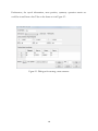
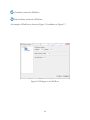
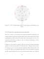
USER MANUAL (V1.18.5) PTCLab -- A free and open source program for calculating phase transformation crystallography Xinfu GU Supervisor: Prof. W.-Z. Zhang and Prof. Tadashi Furuhara Email: [email protected] 2014.1.28 Table of Contents 1 Introduction .................................................................................................................................... 7 1.1 Purpose.................................................................................................................................... 7 1.2 About PTCLab........................................................................................................................... 7 1.3 Functions ................................................................................................................................. 8 1.4 Advantage ..................................................................................................................................... 9 1.5 Download .................................................................................................................................... 10 1.6 Installation for Windows .............................................................................................................. 10 1.7 Main interface ............................................................................................................................. 11 1.7.1 Menu and toolbar ................................................................................................................. 11 1.7.2 Plot toolbar ........................................................................................................................... 13 1.8 Acknowledgement ....................................................................................................................... 15 2 Crystal structure ............................................................................................................................ 17 2.1 Methods for inputing structures .................................................................................................. 17 2.2 Convention of the crystal coordinate system ............................................................................... 19 3 Pole figures.................................................................................................................................... 23 3.1 Basic steps to plot a pole figure.................................................................................................... 23 3.2 About the control panel ............................................................................................................... 25 3.3 Further option for plot ................................................................................................................. 27 3.3.1 Index appearance.................................................................................................................. 27 3.3.2 Index modification and add text ............................................................................................ 27 3.3.3 Symmetry operation ............................................................................................................. 29 3.3.4 Wulff net............................................................................................................................... 30 3.3.5 Complex pole figures with more than one crystal .................................................................. 32 4 Phase transformation crystallography ........................................................................................... 37 4.1 Martensitic transformation .......................................................................................................... 37 4.1.1 Classic PTMC ......................................................................................................................... 37 4.1.2 Double shear version of PTMC .............................................................................................. 40 4.2 Invariant line model ..................................................................................................................... 43 4.2.1 Invariant line in direct space.................................................................................................. 43 4.2.2 Invariant line in reciprocal space ........................................................................................... 45 4.3 O-line model ................................................................................................................................ 47 4.3 E2E model .................................................................................................................................... 50 4.4 3-D NCS method .......................................................................................................................... 55 4.5 Moiré fringe and g method ....................................................................................................... 58 4.6 O-lattice theory............................................................................................................................ 61 4.7 Matching distribution method ..................................................................................................... 62 4.8 Large misfit system ...................................................................................................................... 63 4.9 Variants ....................................................................................................................................... 65 5 Calculation pad .............................................................................................................................. 72 5.1 Single phase ................................................................................................................................. 72 5.2 Two phases .................................................................................................................................. 73 5.3 Matrix operation .......................................................................................................................... 74 5.4 Orientation matrix ....................................................................................................................... 75 5.5 plot 2-D atoms ............................................................................................................................. 76 6 Diffraction Pattern and X-ray Profile .............................................................................................. 77 6.1 TEM diffraction pattern ............................................................................................................... 77 6.2 Kikuchi Map ................................................................................................................................. 79 6.3 Index a TEM diffraction pattern ................................................................................................... 80 6.4 Simulation EBSD pattern .............................................................................................................. 82 6.5 Index EBSD pattern ...................................................................................................................... 84 6.6 X-ray diffraction profile ................................................................................................................ 85 7 Coming features with PTCLab ........................................................................................................ 87 6 Chapter 1 Introduction 1.1 Purpose R eproducible crystallographic features (such as orientation relationship, interface, interfacial defects) are often observed in phase transformation and epitaxial process. This preferred phenomenon usually can be rationalized with the help of geometry analysis. The well-known case is the phenomenal theory for martensitic crystallography proposed in 1950s. The geometry method based on geometrical misfit analysis is simple and takes lattice information sometimes orientation relationship as an input, and it can output rich information about crystallographic features and strain distribution which is useful for studying variant selection. However, various crystallography models usually make users frustrated, since there is no public integrated software for calculating phase transformation crystallography and illustrating the final results. Therefore, PTCLab comes out. PTCLab is an abbreviation of Phase Transformation Crystallography Lab. The purpose of this program is to calculate the transformation crystallography after a phase transformation and represent the results in graphical way such as in stereo graphic projection. The lattice matching near the interface, the superimposed diffraction patterns and so on can be readily simulated with present program. PTCLab is general for all crystal systems. This program is free, open source and runnable on multiple platform. 1.2 About PTCLab PTCLab is developed with Python based on Matplotlib and Numpy library for plotting and numerical calculation. The phase transformation crystallography method adopted in 7 the program is well documented in the literatures (such as Zhang W Z, Weatherly G C. On the crystallography of precipitation[J]. Progress in materials science, 2005, 50(2): 181292). 1.3 Functions The program is designed for general purpose, and it is not limited to special crystal structure. The abilities are described below: I. The crystal structure • Create crystal structures manually or input from CIF file • Simulation of electron diffraction patterns and X-ray diffraction profile • Determine the most close packed planes and directions which are essential for transformation crystallography II. Stereo graphic projection • Showing low indexed planes or directions by symmetry operation • Manually added poles and big circles • Simulating superimposed pole figures according given orientation • Generate the variants of the same orientation relationship according to the lattice symmetry III. Transformation crystallography • Generate or transformation between different representation of the orientation relationship, such as miller indices expression to Euler angle 8 • Calculate orientation relationship according to different criteria, such as O-line method, edge-to-edge method, martensite theory (both single shear and double shear version, Invariant line model) with output in clear Table form... • Plot lattice matching in the interface and readily to be output for energy study • Illustrate superimposed lattice matching such as 3-D near coincidence site lattices method, and can calculate near coincidence site lattice percentage calculation within different directions and planes, and show the result in stereo graphic projection • Electron (TEM) diffraction simulation IV. Calculation pad • Calculate the length and angle between different vectors for one crystal structure or two crystal structures at specified orientation relationship • Find the orientation relationship for a given orientation matrix • Generate orientation matrix with different ways, such as Euler angle, axis pair etc. • Plot atomic lattice • Simple plot of X-ray diagram and show peak list 1.4 Advantage • Free, open source, support Windows and Linux operate system • General for every crystal structure • Publication quality illustration 9 • Both martensite and precipitation transformation, contain various recent developed crystallographic models 1.5 Download The reference websites are: 1. https://code.google.com/p/transformation-crystallography-lab/ 2. http://itclab.weebly.com/ 3. http://sourceforge.net/projects/tclab/ (Download) Search “PTCLab crystallography” by Google, and one can also find the link. Note: Some virus protection software will delete the download file. Please select something like ''allow the file from above link''. 1.6 Installation for Windows The install file is about 15M named as setup.exe. Double click it, and it will show the install interface as Fig. 1.1. (Note that: in some cases, the virus protection program may block this, please allowed this setup to run if you want to install the program.) Click next in Fig. 1.1, and then it goes to Fig. 1.2 to select your install directory. Click next button and then it will install the program automatically. 10 Figure 1.1. Setup interface Figure 1.2. Install directory 1.7 Main interface 1.7.1 Menu and toolbar 11 When you run PTCLab from your desktop, the main interface will be shown as Fig. 1.3. Figure 1.3. Main interface of PTCLab There are fifteen icons on the toolbar: Open a structure file Create a structure file manually Printer for print Clockwise rotation for stereo graphic projection or diffraction patterns Anti-clockwise rotation for stereo graphic projection or diffraction patterns Move the text labels on the stereo graphic projection or diffraction patterns Merge the figures for stereo graphic projection or diffraction patterns so that superimposed figures can be generated. 12 Exit the program Plot Wulff net Clockwise rotation for Wulff net Anti-clockwise rotation for Wulff net Restore the Wulff net to original position Calculate pad for simple crystallography calculation Setting for stereo graphic projection and Wulff net Information about the program 1.7.2 Plot toolbar The figures in this project are all generated by Matplotlib (http://matplotlib.org/). All figure windows come with a native navigation toolbar, which can be used to navigate through the data set. Here is a description of each of the buttons at the bottom of the toolbar adopted from their official website. The Forward and Back buttons. These are akin to the web browser forward and back buttons. They are used to navigate back and forth between previously defined views. They have no meaning unless you have already navigated somewhere else using the pan and zoom buttons. This is analogous to trying to click Back on your web browser before 13 visiting a new page –nothing happens. Home always takes you to the first, default view of your data. For Home, Forward and Back, think web browser where data views are web pages. Use the pan and zoom to rectangle to define new views. The Pan/Zoom button. This button has two modes: pan and zoom. Click the toolbar button to activate panning and zooming, then put your mouse somewhere over an axes. Press the left mouse button and hold it to pan the figure, dragging it to a new position. When you release it, the data under the point where you pressed will be moved to the point where you released. If you press ‘x' or ‘y' while panning the motion will be constrained to the x or y axis, respectively. Press the right mouse button to zoom, dragging it to a new position. The x axis will be zoomed in proportionate to the rightward movement and zoomed out proportionate to the leftward movement. Ditto for the y axis and up/down motions. The point under your mouse when you begin the zoom remains stationary, allowing you to zoom to an arbitrary point in the figure. The Zoom-to-rectangle button. Click this toolbar button to activate this mode. Put your mouse somewhere over and axes and press the left mouse button. Drag the mouse while holding the button to a new location and release. The axes view limits will be zoomed to the rectangle you have defined. There is also an experimental ‘zoom out to rectangle' in this mode with the right button, which will place your entire axes in the region defined by the zoom out rectangle. The Save button. Click this button to launch a file save dialog. You can save files with the following extensions: png, ps, eps, svg and pdf. It is highly recommended to save the 14 figure as pdf, ps, eps, or svg so that it can be further edited with free software Inkscape or commercial software CorelDraw or Adobe Illustrator without losing quality. 1.8 Acknowledgement Special thanks to those contribute to the public resources referred in this project. They are: 1. http://rruff.geo.arizona.edu/AMS 2. http://quantumwise.com/publications/tutorials/mini-tutorials/ 3.Pymmlib: http://pymmlib.sourceforge.net/ 4.pdfgui: http://www.diffpy.org/products/pdfgui.html 5.WxFormBuilder: http://sourceforge.net/projects/wxformbuilder/ 6. http://wiki.scipy.org/Cookbook/Matplotlib/Drag_n_Drop_Text_Example 7.Icons from Snipicons by Snip Master: https://www.iconfinder.com/search/?q=iconset:snipicons 8.Mixin for wx.grid 15 16 Chapter 2 Crystal structure F irst of all, the application of PTCLab requires one to input the crystal structure first. Depending on user's interest, one or more than one structure information are needed to be input. There are two ways to do this. 2.1 Methods for inputing structures There are two ways to input the crystal structures in PTCLab: a) The first way, if you have the CIF (Crystallographic Information File) files, just click the icon , and select the structure once in a time. The CIF file could be found from the internet, such as http://rruff.geo.arizona.edu/AMS/amcsd.php b) The second way, create the file by user themself. Click , you will find the dialogue to construct the structure, as shown in Figure 2.1. When you finish the table, do not forget to save it, and you can use it later by method (a). As for the dialogue, crystal name could be arbitrary, Space group could not be important, if you know all the atoms about the structure, or if you are interested in the lattice itself. Lattice parameters for the crystal structure could be found from the literatures. For the “Fractional atomic coordinates”, you can add and delete by the button “Add+”. For Mg (hcp) structure, it is shown in Figure 2.1. When you click ok button in Figure 2.1, the structure info will be added to the Main frame of PTCLab as tree item as shown in Figure 2.2 with three sub items, i.e. crystal info., stereo proj (Chapter 3). and diff. pattern (Chapter 4). By clicking ‘‘crystal info'', one can visualize the crystal structure as shown in Figure 2.3. Different colors and size are for different atoms. One can drag the crystal structure by mouse to any view direction. The crystal structure could be saved, zoom in/out and restore by the Plot toolbar. 17 Furthermore, the crystal information, atom position, symmetry operation matrix etc. could be viewed from other Tabs on the frame as in in Figure 2.3. Figure 2.1. Dialogue for creating a new structure 18 Figure 2.2. A crystal structure is added to the root of PTCLab Figure2.3. The left side is Mg (hcp) crystal, and the right figure is MgO structure 2.2 Convention of the crystal coordinate system As we know, there are six parameters to define a crystal structure, i.e. a, b, c, , , , as shown in Figure 2.4(a). Generally, we need to set up an orthogonal coordinate system(x,y,z) so that the vectors in crystal coordinate (e1,e2,e3) could be manipulated with 19 knowledge in Cartesian coordinate system. Mainly, there are two conventions are applied as shown in Figure 2.4(b-c). In Figure 2.4(b), the x axis is set to be parallel to e1 and e3 is fixed in the plane x z, while in Figure 2.4(c), the z axis is set to be parallel to e3 and e1 is fixed in the plane x z. Though the selection of the different coordinate system conventions would not affect final result, but cautions must be paid in some cases, especially when you apply Euler angle in EBSD system, the alignment of the coordinate system is essential. When different coordinate system is selected, the Euler angle and the resulting orientation matrix would be different. In PTCLab, the convention of Figure 2.4(b) is adopted. Figure 2.4. Coordnate system (a) Six lattice parameters of a given crystal, (b) definition of orthogonal coordinate system with x//a, (c) definition of orthogonal coordinate system with z//c. 20 22 Chapter 3 Pole figures T he basic procedure to plot a pole figure can be found from the textbook. The details will not be reproduced here. Three conventions are applied in PTCLab, (1) the projection direction is from South Pole to North Pole, (2) the projection direction is pointing out of the screen, (3) right-handed coordinate system is adopted. 3.1 Basic steps to plot a pole figure As in many other functions in PTCLab, the initial parameters have been set beforehand. Users can run the software to get a rough impression of it. The basic steps to plot a pole figure are: (1) The first step is to create a crystal structure, see Chapter 2. (2) Click ‘‘stereo proj'' from the tree items at left side of the main frame under the crystal structure you created. Pole figure window will appear as shown in Figure 3.1. The right side of the pole figure window is the control panel for plot the pole figures (Section 3.2 for more information about control panel). (3) Click ‘‘Plot figure'' button at the bottom of the control panel, and pole indices smaller than 1 will be shown, as Figure 3.2. (4) The index and big circle can be turned on by clicking the option ‘‘Show'' on the control panel. (5) Further refinement, see Section 3.3. 23 Figure 3.1. Pole figure window Figure 3.2. [001] pole figure of Mg (hcp) 24 3.2 About the control panel The control panel is shown in Figure 3.3. It provides most information about plotting pole figure. • Structure Info, the information about crystal structure. It is automatically generated when user create the crystal structure, and cannot be modified. • Pole Figure Info, set the Projection direction and set the orientation of the pole figure by specifying Horizontal direction. These two directions must be normal to each other. These two directions must be normal to each other. These direction can be specified by users or could be by Euler angle ( ZXZ convention ), i.e. Projection direction // Normal direction (ND), Horizontal direction // Rolling direction (RD). • Pole range, set the how many indices to be plotted. There are two ways. The first one is plot the indices with their length smaller than certain value. This could be useful to show the symmetry of the poles. The second way is to plot the indices with their maximum number smaller than certain value. • Type, set the index type to be crystal direction or plane normal (reciprocal vector), since we know that the same direction when it represents crystal direction or plane normal could have different index. • Style, set the properties (color, size, line style) of pole or big circle, change it before plotting. • Index Setting, turn on/off the Index or Big circles. These options could be activated after plotting poles. • Add Data, to add one specific pole (SP) or Big circle (BC). A set of index could be added by clicking the button ‘‘...''. 25 • Clear Figure, clear all of the items in the pole figure. • Undo, undo previous step, if wrong index is plotted. • Plot Figure, to plot the poles according to the above setting conditions. Figure 3.3. Control panel for pole figure 26 3.3 Further option for plot Further options could be applied to improve the plot as showing below. 3.3.1 Index appearance Sometimes the index appearance shown in Figure 3.2 is unsatisfied. The minus sign is needed to put onto the numbers as an overbar. This has been done with TEX with Matplotlib package. The option can be set by clicking on Toolbar, and the setting window is shown in Figure 3.4. • Font size, font size of the index • Font color, font color of the index • Boxed Index BG color, to set background color of the index • Transparency, to set the transparency of the background color • Index with TEX, to change the minus sign as overbar • Ok, to apply the setting • Cancel, to close the window without any change After setting, turn off original index, and turn on again from the control panel. The new style index will be shown, as shown Figure 3.5, compared with Figure 3.2. As shown in 3.5(b), four index convention are default setting for Hexagonal crystals. 3.3.2 Index modification and add text The position of the index could be moved by clicking on the main tool bar and move the index text to where as you want. This could be helpful for complex pole figures. The color and text font size could be changed from the “Edit” menu by clicking corresponding option then click the index. The color and text font could be set in the 27 dialogue shown in Figure 3.4. In addition, index could be deleted from the same menu. Text could also be added from the “Edit” menu, Figure 3.4. Setting dialogue for pole figure (a) (b) Figure 3.5. New index style as in FCC (a) and HCP (b) structure 28 3.3.3 Symmetry operation 3.3.3.1 Add a set of index A set of index could be added by clicking the button ‘‘...'' on the control panel and a dialogue as Figure 3.6 will be shown. One can add poles and Big Circles respectively. ‘‘Add+'' is add an index a time, while ‘‘Add++'' could add all of the equivalent directions (variant) due to the symmetry operation. In Figure 3.6, all of the equivalent crystal direction <112> is added at the same time. The example shown here is FCC (face centered cubic) structure, and generally there are 24 variants. The projection of these directions in [001] pole figure is shown in Figure 3.7. Figure 3.6. Dialogue to add crystallographic equivalent index 29 Figure 3.7. Show <112> variants with red square markers 3.3.4 Wulff net The Wulff net can be plotted and rotated with PTCLab. The setting dialogue can be shown by clicking on Toolbar, and the setting window is shown in Figure 3.8. • Longitude and Latitude, to set the separation angle for longitude and latitude respectively. The default value is 5 degrees. • Rotation speed in degree, to set the rotation step around the axis normal to the screen. • Grey level, to set the color of the Wulff net. After setting, the plot of Wulff net could be plotted by clicking icon on Toolbar Plot Wulff net 30 Clockwise rotation for Wulff net Anti-clockwise rotation for Wulff net An example of Wulff net is shown in Figure 3.9 in addition to Figure 3.7. Figure 3.8. Dialogue to set Wulff net 31 Figure 3.9. Wulff net example 3.3.5 Complex pole figures with more than one crystal 3.3.5.1 Combination of two pole figures at an orientation relationship Composite pole figures are useful in studying phase transformation, and they could be constructed by superimposing two pole figures at a given orientation relationship, i.e. plot the pole figure respectively, and then combine them together by pressing window Toolbar. When pressing on the main , a window shown in Figure 3.10 will pop up, one can combine figures that they have plotted by press the “add” button. Here we take the Kurdjumov-Sachs orientation relationship (111)fcc//(011)bcc and [101]fcc//[11-1]bcc in FCC/BCC system as an example. The figures plotted in next three steps are shown in Figure 3.11(a-c) respectively. (1) Plot the FCC [10-1] pole figure with horizontal axis parallel to (111) in red color 32 (2) Plot the BCC [11-1] pole figure with horizontal axis parallel to (011) in blue color (3) Press , add both pole figures in (1) and (2), and save the results. Figure 3.10. Combination window (a) (b) 33 (c) Figure 3.11. (a) FCC [10-1] pole figure, (b) BCC [11-1] pole figure, (c) Combinations of (a) and (b) 3.3.5.2 Variant due to equivalent orientation relationship Due to the symmetry of the crystal, several equivalent orientation relationships exist between the phase transformation products and the matrix. Such products with equivalent crystallography are called variants. The number of the variants depends not only on the symmetry of the product and matrix, but also the orientation relationship, as will be shown in following examples. In Figure 3.6, it has a button “set poles by OR”. One can set the orientation relationship between the matrix and the products by clicking this button. Dialogue shown in Figure 3.12 will pop up. One can set the orientation relationship (OR) between Crystal 1 and Crystal 2. The OR is set by orientation matrix which is one of the methods to represent the OR in rigorous manner. If one do not know the orientation matrix, one can click the 34 “Generate OR” to generate the orientation matrix by conventional parallel representation. The dialogue is shown in Figure 3.13, one can set direction parallel at “uvw” section and set plane parallel at “hkl” section. Further rotation is allowed to deviate from above rational orientation. When the rotation axis is 001, it is the rotation around the plane normal set in “hkl” section. When the rotation axis is 100, it is the rotation around the direction set in “uvw” section. The rotation angle is in degrees. When the setting in Figure 3.13 is finished, click the “OK” button and the OR in Figure 3.12 will be automatically generated. In Figure 3.12, “All variants of the OR” means taking all the symmetry operation into account, and “With notation of OR number” means numbering each pole when plotting, i.e. the poles with the same OR will have the same number. The specific directions (specified in the last line, here [100]) in crystal 2 will show in the pole figure of Crystal 1 (matrix). The option “with all vector families” will show all equivalent directions of the specified direction in Crystal 2. For the well-known Kurdjumov-Sachs orientation relationship, there are 24 variants. All the <001> directions in BCC crystal variant are shown in [111] pole figure of FCC crystal as shown in Figure 3.14(a). If <123> directions in BCC variants are selected, more complex figure could be obtained shown in Figure 3.14(b). Nevertheless, the symmetry of the FCC crystal could be found from the pattern. Figure 3.12 Dialogue for the equivalent orientation relationship between two phases 35 Figure 3.13 Dialogue to generate OR matrix (a) (b) Figure 3.14 (a) <001>and (b) <123> directions in 24 BCC variants are shown in [11-1] pole figure of FCC crystal. 36 4 Phase transformation crystallography T he phase transformation crystallography models are generally geometric models. The main concept is to consider the matching in the interface by assuming best matching1 indicates lowest the interfacial energy or to require the minimization of the macroscopic strain. Therefore, the OR corresponding to the lowest interfacial energy or minimum elastic energy would be preferred. Sometimes, the OR is taken as an input, and analyzes the three dimensional matching and find the candidate interface. For martensitic transformation, the famous crystallography theory is phenomenal theory of martensite crystallography (PTMC) for twinned martensite. The subsequently developed double shear models are for lath martensite etc. As for diffusional transformation, the structural ledge model or its extension of the near coincidence sites (NCS) method, O-line model and later developed g theory, and the Edge-to-Edge (E2E) matching. None of the model could predict all the observations so far. PTCLab incorporate most of the theories as stated below. However, it will not reproduce the theories here. 4.1 Martensitic transformation 4.1.1 Classic PTMC The details of classic PTMC could be found in Wayman’s book “Introduction to the crystallography of martensitic transformations”. The menu for PTMC calculation could be found under the menu of “Calculation” on the main frame. The input of PTMC usually includes: (1) Lattice parameters 1 Good matching means when two crystals are interpolated with each other, the atoms from two crystals are close to each other. The coincidence site lattice point is a good matching point. However, in general system, coincidence site lattice does not exist, and only near coincidence site lattice exist and these locations are defined as good matching area. 37 (2) Lattice correspondence (3) Twin/slip system, i.e. lattice invariant shear system There are shown in Figure 4.1. Dilatational factor in Figure 4.1 is the parameter proposed by BM in addition to their original PTMC theory in trying to solve lath martensite crystallography. In default, it is 1.0, i.e. the habit plane in PTMC is true invariant plane. As for the shear system, unlike slip system, one only needs input the twin plane and the shear direction will be found by the program in a consistent way. This treatment is more useful for system like HCP/BCC, since the shear direction for the twinning martensite is irrational. The lattice correspondence can be input by user. For common FCC/BCC or HCP/BCC system, the stored value can be used. For unknown system, the lattice correspondence could be found in Section 4.6 by finding nearest neighbors. After setting, press the OK button, one will get the result like Figure 4.2 in a table form. The content can be copied with “Ctrl + c” after selection with mouse. Figure 4.1 Input dialogue for PTMC 38 Figure 4.2 Output results of PTMC In Figure 4.2, first four lines show the input information, and the rest is the results. Generally, there are four solutions. From the results, it can be found that the first solution and the fourth solution are equivalent, and so are the second one and the third one. There are many abbreviations for reduce the length. The meanings are (same for Tables afterwards): SG: Space group Lattice C.: Lattice correspondence Delta: Dilatational factor IL (in 1): Invariant line in crystal 1 in direct space 39 IL (in 2): Invariant line in crystal 2 in direct space IL* (in 1): Invariant line in crystal 1 in reciprocal space IL *(in 2): Invariant line in crystal 2 in reciprocal space RB: phase transformation matrix represented in the orthogonal coordinate system of crystal 1 specified in Section 2.2 OR Mat. : Orientation matrix, describing the parallel relationship between crystal 1 and crystal 2 in 3-D space HP (in 1): Habit plane in crystal 1 HP (in 2): Habit plane in crystal 2 Macro s: macroscopic shear direction m2: the magnitude of the macroscopic shear direction F: macroscopic deformation matrix m1: magnitude of the shear for the input shear system plane: the deviation angle between the planes for description of orientation relationship direction: the deviation angle between the directions for description of orientation relationship The twin ratio is inverse proportional to m1, therefore for the case in Figure 4.2, the twin ratio is 0.42222/0.24444 = 1.73 : 1, i.e. the volume fraction of smaller m1 is 63.3%. Note: If there are no solutions or input is incorrect, the program will remind you. 4.1.2 Double shear version of PTMC When the classical PTMC cannot explain the observations in lath martensite, double shear version of PTMC is proposed. Classical PTMC is known to be treated as single shear. 40 With proper combination of two lattice invariant shear systems, the crystallography of lath martensite could be explained as shown by Kelly. The modified version of PTMC is more flexible, and the results depend on two input lattice invariant shear system. In addition, there is one additional degree of freedom to be fixed, and this is usually done by setting the magnitude of one of the lattice invariant shear system. In PTCLab, the second shear can be fixed manually. The input dialogue is shown in Figure 4.3 which is similar to Figure 4.1. Two shear systems are needed and the restriction on the second shear magnitude should be applied. When press “OK” button, the output is similar to Figure 4.2, except there are no true invariant lines here, therefore the IL section in output table is skipped. As mentioned earlier, there is a special solution of double shear version of PTMC as show by Kelly. In this special solution, the interface contains two set of dislocations with one of set as screw dislocation. The Kelly’s solution is separated in PTCLab, and the magnitude of the second shear is automatically generated by the program, and the shear directions are fixed for full dislocation, therefore, the shear planes can only be varied. The result is shown in Figure 4.4. Two set of dislocation line direction and their spacing are added. Though, there are four solutions, generally, the smaller shear magnitude is preferred. In addition, the calculated results should be consistent with the experimental results. Therefore, the solution 1 is a better choice. 41 Figure 4.3 Input dialogue for double shear version of PTMC Figure 4.3 Input dialogue for Kelly’s proposal Figure 4.4 Output results of Kelly’s proposal for double shear version of PTMC 42 4.2 Invariant line model 4.2.1 Invariant line in direct space The invariant line model proposed by Dahmen could be applied to explain the preferred growth direction and orientation relationship in precipitation and epitaxial system, since the invariant line is a geometric best matching direction. There are infinite invariant lines (lying on a cone) in some systems, and the invariant line usually confined in a rational plane (low indexed/slip plane) in considering of the dislocation nucleation. In general, the invariant line needs the input: (1) Lattice parameters (2) Parallelism of rational planes (the final invariant line lies in this plane) (3) Two pairs of close related vectors (like the lattice correspondence in PTMC) Take FCC/BCC system for example, the close packed plane (111)fcc//(011)bcc is set to be parallel to each other at the Kurdjumov-Sachs orientation relationship. Next we will apply the invariant line model to confine the rotation within (111)fcc//(011)bcc and determine the invariant line direction. The more difficult part is Input (3), and one need to input two pairs of close related vectors. It can be done by plot the atoms on (111)fcc//(011)bcc at Kurdjumov-Sachs orientation relationship by Calpad in PTCLab (see Chapter 5), and the results is shown in Figure 4.5, and one can find two arbitrary pairs of vectors around the origin, i.e. 1/2[10-1]fcc//1/2[11-1]bcc and 1/2[01-1]fcc//1/2[-11-1]bcc. After input the vectors into Figure 4.6 and press “OK” button, one can get the results as Figure 4.7. There are two crystallographic equivalent solutions. From the second solution, one can see that the final result by invariant line model is close to Kurdjumov-Sachs OR with a deviation angle about 0.45°. The invariant line direction is close to [10-1]fcc. The atomic matching at the calculated OR can be plot by the dialogue shown in Figure 4.6. First, input plane normal (111) for crystal 1 (FCC) and press plot, and then input the plane 43 normal (011) for cystal 2 (BCC) and press plot. Cleary, the invariant line goes along the best matching direction as shown in Figure 4.6. One can modify the range of plot after the “range”, and it is arranged like –x x –y y –z z. Figure 4.5 atomic matching on (111)fcc//(011)bcc at Kurdjumov-Sachs orientation relationship Figure 4.6 Input dialogue for invariant line model 44 Figure 4.7 Output dialogue for invariant line model 4.2.2 Invariant line in reciprocal space The invariant line model in reciprocal space mathematically is much similar to the invariant line in direct space. The concept originated from the diffract patterns where multiple g vector difference (called g) is normal to the interface. When multiple gs are parallel to each other, there are an invariant line in reciprocal space, of course there is also an invariant line in direct space but not necessarily lie in an rational plane. However, the invariant line model restricts the reciprocal invariant line normal to two parallel directions (zone axis). Similar to section 4.2.1, it requires two pairs of correlated g vectors as an input. The g vectors could be found from the diffraction patterns (since the defined g is normal to the interface) or plot the diffraction patterns (see Chapter 6) at reported OR or at closed rational OR. The correlated g vectors at Kurdjumov-Sachs OR are (111)fcc//(01-1)bcc and (200)fcc//(10-1)bcc. After input and press “OK” in Figure 4.8, the result will show as Figure 4.9. The output includes orientation relationship and the habit plane normal. The direction/plane normal in PTCLab are indexed in both Crystal 1 and Crystal 2, therefore one can compare their experimental results with the calculation result thoroughly. Note: this calculation dialogue can be also applied to E2E model (section 4.3). 45 Figure 4.8 Input dialogue for reciprocal invariant line model Figure 4.9 Output dialogue for reciprocal invariant line model 46 4.3 O-line model The O-line model is developed from the O-lattice theory. The main concept is that the candidate habit plane contains periodic good matching zone, and the good matching zone is infinite along one direction (invariant line direction), i.e. the interface contains only one set of dislocation. The O-line model needs inputs: (1) Crystal parameters (2) Lattice correspondence (3) The Burgers vector (4) Criterion (since there is one degree of freedom unfixed, there are numerous solutions for the interface containing one set of dislocations) There are five criterions as shown in Figure 4.10, and each of them could fix the freedom. Maximum dislocation spacing, since larger dislocation spacing may imply lower interfacial energy Minimum plane deviation. This consideration is from easy nucleation view. Minimum direction deviation. This consideration is from easy nucleation view. Dislocation lying in the given plane. This consideration is from dislocation nucleation, and the output has the same result as PTMC, if the same condition is inputted. Arbitrary angle between the correlated Burgers vector (all the O-line solutions can be numerated) There are three optional buttons to assistant the input. Show correspondence vectors of a set equivalent direction of the Burgers vector. For example, the correspondence vectors of {-1 0 1}fcc/2 are shown in Figure 4.11. 47 From the results, one can see there are two types of correspondence according to the direction in Crystal 2, i.e. {111}bcc/2 and {100}bcc/2. Therefore, the results for [-101]fcc/2 and [1-10]fcc/2 are different. With correspondence. There are two such buttons, and one is to get the correspondence plane for Crystal 2 after user input the plane for Crystal 1, while the other is to get the correspondence direction for Crystal 2 after user input the direction for Crystal 1. The output of the O-line model is shown in Figure 4.12 with criterion 2. There are two solutions, and they are equivalent to each other. The O-line model can output the dislocation spacing (Disl. Spc. in Figure 4.12) with the same unit as lattice parameter (Angstrom here). Figure 4.10 Input dialogue for O-line model 48 Figure 4.11 Correspondence vectors of {-1 0 1}fcc/2 Figure 4.12 Output of O-line model 49 4.3 E2E model In the edge-to-edge matching model, the first step is to find the possible close packed or nearly close packed directions (atomic rows) from Crystal 1 and Crystal 2 and to set them to be parallel each other. The parallelism is indicated from interfacial energy consideration. The second step is to find the matching planes (possible close packed or nearly close packed plane) containing the directions defined in step one. Till now, one can define a rational orientation relationship by setting the directions and planes to be parallel to each other. The OR should be refined so that the planes are matching at the interface by an edge-to-edge matching manner. The method shown in Section 4.2.2 is applied here, i.e. gs defined by the matching plane are parallel to each other. The input of E2E model requires (ref. Figure 4.13): (1) Up limit of the row misfit, f_r, restrict the possible atomic rows to good matching ones. (2) Up limit of plane matching, f_d, restrict the possible planes to good matching ones. (3) The criterion that which plane is close packed or near close packed. The planes should have physical meaning. In PTCLab, the planes are found by the simulated X-ray intensity. Therefore, one need specify how many gs are considered or the intensity above which should be considered. (4) Interact parameter which is related to atomic rows which could be derived from the planes. The default value is 1. If one cannot found satisfied directions, please increase the number. After setting, press the “Set the parameter” button. Next go to output session, one can (1) plot the atoms at any plane of Crystal 1 or Crystal 2. For example, Figure 4.14 shows atoms on (111) plane in FCC, and the color is set according to the elements. 50 (2) show all g list in Crystal 1 and Crystal 2 (3) show most close packed plane and directions with press “Table” button, one can also modify the table, add/delete the direction or planes. (4) show matching figure. The matching figure should be processed before refinement! That is user need to check the plane matching, direction matching and their combinations in sequence. (5) show possible nominal rational ORs (6) refinement of the rational ORs with gs parallel method Figure 4.13 Input dialogue for E2E model 51 Figure 4.14 Atoms on (111) plane in FCC Figure 4.15 g list in FCC with none zero structure factor Figure 4.16 Candidates of possible close packed or near close packed planes and directions in FCC and BCC structure 52 In FCC/BCC system, the candidate planes and atomic rows are shown in Figure 4.16. The misfit between all candidate planes is shown in Figure 4.17(a). The minimum matching between the planes are between {111}fcc and {011}bcc. The atomic misfit between all candidate atomic rows is shown in Figure 4.17(b). The minimum matching between the directions are between <1-10>fcc and <11-1>bcc. By applying the criterion of the misfit, the combination of the plane and directions is shown in Figure 4.17(c). For each candidate atomic row, the candidate plane contains this direction are searched and shown right side of each row, i.e. for atomic row <1-10>fcc//<11-1>bcc, there are three candidate plane pairs: {111}fcc/{011}bcc, {002}fcc/{011}bcc, and {220}fcc/{112}bcc. The rational OR is shown in Figure 4.18. Solution No.1 is N-W OR while No.4 is K-S OR, and No. 5 is Pitsch OR. (a) (b) (c) Figure 4.17 An FCC/BCC system (a) Plane matching with misfit smaller than f_d, (b) Direction matching with misfit smaller than f_r, (c) Possible combination of (a) and (b). 53 Figure 4.18 Rational ORs from E2E model Figure 4.19 Refined ORs based on g parallel method 54 Refinement (requiring plane pairs E2E matching) of the rational OR in Figure 4.18 is carried out by using g parallel method (a general description of E2E matching), therefore if one knows correlated g vectors, one can also apply method in Section 4.2.2 to calculate the crystallographic features. The refinement here is automatically done by PTCLab, the results are shown in Figure 4.19, by pressing “Refine” button shown in Figure 4.13. Rational OR1 has two solutions by g parallel method while OR 2 has no solution and “Need manual refinement (judgment)”. The OR 3 is found duplicated with OR 1, and it shows “duplicated with previous OR”. In the refinement, there are would be a deviation around the parallel atomic row, that is why some rational OR after refinement could be coincided. 4.4 3-D NCS method As mentioned before, the geometric models for phase transformation crystallography consider atomic/lattice matching. A graphic way named 3-D near coincidence site (3-D NCS) method originated from structural ledge model could be applied. The method is simple but takes much computational time. The calculation follows “Furuhara, T., T. Maki, and K. Oishi. Metal. and Mater. Trans. A 33.8 (2002): 2327-2335”. The inputs for 3-D NCS method are: (1) Crystal lattice parameters (2) Orientation relationship matrix (Manually or from experimental data) (3) Interest range (The larger is the system, more time is taken to process) (4) If searching in 3-D, the step of the interface orientation will be needed. Default value is 1. Select 3-D NCS method from “Calculation” menu, a tab window will pop up, see Figure 4.20. The left part of Figure 4.20 is plotting area (could be viewed at any direction by mouse), and the right part is control panel. The control panel includes: 55 Structure Info: structure information, selectable. OR matrix: orientation relationship matrix Plotting geometry: plot the NCS and atoms with the given axis and range. NCS criterion (in unit of lattice parameter a) specifies the range below which the atom/lattice matching could be treated as NCS. Plot setting: set the marker type, size, and color. The “Gradient” option could be selected and the plot will show the NCS with gradient color according to the misfit value. Crystal 1/2: plot the atoms in Crystal 1/2 in the specified axis and range. Plot NCS: plot the good matching atoms in the specified axis and range Clear: clear all plots NCS Map: 3-D NCS statistical analysis for different plane and direction, with the plane/direction step specified by user at the textbox beside the “Plot NCS” View: view along given direction, the direction could be in the crystal coordinate system or plot coordinate system Statistics: show percentage of NCS atoms, total atom number, best matching plane/direction when apply NCS map. One of examples is plotting the atoms and NCS on specified plane. The well-known example in textbook is structural ledge model. The interface would prefer the stepped interface rather than planar one. Figure 4.21 shows the NCS distribution at three neighbor (111) layers at N-W OR. One can see that the NCS distribution on single (111) plane (blue solid circle) and the NCS percentage is about 7.4% (with NCS criterion 10.76%a). As shown in the figure, the NCS on successive layer (red solid circle) of (111) plane connects with previous and so does the green layer. If the interface deviates from (111) plane and pass through these connecting NCS points, the NCS percentage of the plane will greatly improve to about 25%. 56 An example of 3-D NCS map is shown in Figure 4.22. The matching for the whole space could be visualized by NCS percentage. Figure 4.20 Main window for 3-D NCS plot Figure 4.21 NCS at N-W OR for three successive (111) layers. Solid circles are NCS while open circles are atoms on (111) plane. Different color is to show different layers. 57 Figure 4.22 NCS distribution in 3-D space at K-S OR 4.5 Moiré fringe and g method The section is close related to Section 4.4. The last section considered only NCS percentage; however, the NCS cluster distribution could be identified by Moiré fringe and g method. In last Section, the figure can be plotted in 3-D way, however, sometimes people only interested in some specific plane or projection, thus more elegant plots could be done by “3-D NCS (2-D plot)” from the “Calculation” menu. With this plot, one can draw plane traces (Moiré fringe) defined by g. Press “Moiré trace” button on the control panel, the dialogue shown in Figure 4.23 will be shown. The input is (1) g1 and g2 in Crystal 1 and Crystal 2 respectively. Multiple g vectors are supported. g1 and g2 are correlated vectors. The g2 could be generated after g1 is input. This could be done by press “Input g2 with C” and input the corresponding matrix and press “OK”. 58 (2) Set trace line style. (3) Single Moiré plane trace, the default setting is plot series parallel traces, and if single trace is preferred, check this option. An example is shown in Figure 4.24 at near K-S OR in a duplex stainless steel. The red markers in the figure are NCS cluster projected along the invariant line. The Moiré plane traces are periodically passing through the NCS cluster, and NCS clusters are located at the intersections of the Moiré plane traces. In addition, the NCS Map button is enhanced in this 2-D plotting. When this button is pressed, a setting dialogue shown as Figure 4.25 will pop up. It allows user plot 3-D plot or 1-D plot. In 3-D plot, the plot area could be defined as angle range. In 1-D plot, the plot could be set up for planes contain certain axis. The last option in the dialogue is to change the angle pair to crystal direction/plane normal, and vice versa. Figure 4.23 Dialogue for Moiré trace plot 59 Figure 4.24 NCS distribution in 3-D space at near K-S OR in a duplex stainless steel Figure 4.25 NCS plot setting 60 4.6 O-lattice theory O-lattice theory is proposed by Bollmann for calculating interfacial structures (including grain boundary). Present implication of O-lattice theory is included in 2-D plotting of NCS mapping, since there are closely related. For calculating O-lattice, one need input possible Burgers vector and transformation matrix. The transformation matrix is much difficult for general transformation. One way is to get it from different crystallographic models by PTCLab, and the other way is to direct generate it, PTCLab offers such function. Anyway, the main frame for O-lattice calculation is shown in Fig. 4.26. After input the transformation matrix and Burgers vector, one can press `Cal O-lattice` button, and the program will calculate all principal O-lattice vector and possible dislocation spacing etc and show in `Result` box. To illustrate the O-lattice, one can press `Show primary O-vector` for principal O-lattice vector, press `Plot O-lattice` to plot O-lattice point, press `O-cell` to plot dislocation structure. In Fig. 4.26, it shows the dislocation structure on (111) plane at N-W OR. Fig. 4.26 O-lattice calculation 61 4.7 Matching distribution method A natural question would come to mind: for a given OR, which direction is best matching and which direction is worst matching in three-dimensional space. The matching distribution method could be helpful to solve this problem. The only input is OR matrix, and it could come from EBSD test or generate manually. When input in Figure 4.27 is finished, press “OK” button. The best/worst matching direction and their misfit value will be shown. In general, the habit plane could be assumed normal to the worst matching direction so that the habit plane could contain relative good matching direction. Moreover, the application could also output the lattice correspondence matrix. Figure 4.27 Dialogue for misfit analysis application 62 4.8 Large misfit system For the large misfit system, it means thee lattice misfit is so large that one-to-one lattice correspondence is never preserved. The reference state2 would be a coincidence site lattice (CSL), and the interfacial dislocation would be DSCL lattice vector. In general, for an interface, exact CSL/DSCL is impossible since it needs special OR and lattice parameter, and constrained CSL/DSCL (CCSL/CDSCL) will be applied to find the reference state. The find of the reference state is not trivial, even in the same system different reference state could be possible, such as in austenite/cementite system. Again, the reference state could be found by guidance from the reciprocal lattice (diffraction pattern). The input (Figure 4.28) for this application includes: (1) Lattice parameters (2) Three constrained g vectors/crystal directions pairs (in row) After input, press “OK” button, the results will be shown as 2 Reference state means the correspondence in the area between the dislocations after relaxation. 63 The important outputs are constrained lattice parameter for crystal 2 to sustain the CSL structure. The deviation from original lattice parameters should be small. The DSCL lattice vector are shown in rows, and their combination could be served as the Burgers vector of secondary dislocations. The DSCL lattice on a specified constrained plane could 64 be plotted by the dialogue in Figure 4.28. First, set the plane in crystal 1 and plot, secondly, set the plane in crystal 2 and plot, finally, press the DSCL button. The figures could be cleared by press “Clear” button. The interfacial structure for the large system could be analyzed by this kind of figures. Figure 4.28 Dialogue for large misfit system 4.9 Variants Due to the symmetry of the matrix, there are several crystallography equivalent transformation products. These transformation products are called variants. For fcc/bcc 65 lattice, in general, there are 24 variants, as shown in Fig 4.29. For special orientation relationship, the symmetry operator are coincided, thus the number of variant would be reduced. In Fig. 4.30, the variant number of fcc/bcc system change for 24 at K-S OR to 12 at N-W OR. In order to get the number of variant numbers, PTCLab offers a general tool for the purpose in general system. The menu is EBSD/Variant shown in Figure 4.31 containing “Stereo proj.”, “EBSD/reconstruction”, “EBSD analysis” panels. Figure 4.29 Stereo graphic projection of <001> of 24 bcc variants at K-S OR (a) (b) Figure 4.30 Variant number reduce from (a) 24 to (b) 12 66 Figure 4.31 EBSD/Variant main window (1) Number of variants Click the “Set Sym.” button. Window as in Fig. 4.32 will be shown. There are several ways to set the symmetry. User could specify them, because in some publications, the authors have their own preferred sequence and the number indicated in Fig. 4.29 will change. The program stores some setting from the literatures. Anyway, the program can generate the symmetry operation by click “Generate by program. In Fig. 4.32, it shows 12 symmetry operations for fcc/bcc system at N-W OR. Common symmetry between fcc and bcc could also be shown. (2) Change with Euler angle (OR) OR could be generated by specifying Euler angle or by Miller index parallelism like in previous sections. Specific Euler could be changed by click “+” or “-” in Fig. 4.31, or all the Euler angles could be changed by click “+++” or “---”. The change step could be specified. 67 (3) Mis-orientation between variants Minimum mis-orientation between variants could be calculated by present program as shown in Fig. 4.33 by click “OR table”. Specifically, you can get the rotation axis and other features from “EBSD analysis” panel instead of “Stereo proj.” panel. Figure 4.32 Window for setting symmetry Figure 4.33 Mis-orientation angles between variants 68 (4) Group of variants The variants are usually classified into several groups, such as Bain group, close packed plane (CP) or close packed direction group (CD). PTCLab can generate these groups automatically in “EBSD analysis” panel. For example, the CP/CD group can be shown by clicking CP/CD button as shown in Fig. 4.34. Figure 4.34 CP/CD group (5) Generate shape strain Shape strain is important to understand variant accommodation mechanism. The shape strain could be calculated by crystallographic model specified in previous chapter. The shape strain of other variants could be generated based on this by click “Shape strain” button, as shown in Fig. 4.35. The shear direction and shear plane are also shown. 69 Figure 4.35 shape strain (6) Variant at grain boundary. There are several mechanisms for variant selection at grain boundary see T. Furuhara et al. Metall. Mater. Trans. 39 (2008):1003. The four selection rules in Furuhara’s work is implemented in PTCLab. The input is shown in Fig. 4.36. The orientations of two grains are necessary. Other input is not necessary based on different selection rules. An example output is shown in Fig. 4.37. Reader could test the result by using the data in Furuhara’s paper. Figure 4.36 Input for variant selection analysis 70 Figure 4.37 Output based on grain boundary selection rules 71 Chapter 5 Calculation pad C alculation pad (Calpad) is designed to quick access some crystallographic features, such as the angle between planes or directions in single or multiple phases, the plane spacing, change between different description of orientation relationship, plot atoms on specified plane, basic matrix operation ect. The Calpad could be accessed by pressing from the Toolbar on Main window. 5.1 Single phase The dialogue for single phase is shown in Figure 5.1. After select the crystal, the angle between directions (uvw), planes (hkl), or direction and plane can be calculated by press “Calc” button. The table list of the angle between low indexed planes or directions could be obtained by pressing “Table” button. Similarly, the plane spacing or direction length could be calculated. Generally, the plane index is not coincide with the direction index, the transformation between them is offered. For hexagonal system, the 3to4 or 4to3 index for plane or direction is offered on this dialogue. 72 Figure 5.1 Dialogue for single phase 5.2 Two phases The dialogue (Figure 5.2) for two phases is similar to the single phase. For multiple phase, the orientation matrix is needed. It could be generated by press “Generate OR matrix” as mentioned in Section 3.3.5.2. The angle between planes or directions from different crystals can be calculated. The misfit between directions is calculated as length difference. The transformation between different crystal coordinate system is offered. Figure 5.2 Dialogue for two phases 73 5.3 Matrix operation The dialogue for matrix operation is shown in Figure 5.3. The conventional matrix operation could be calculated. The calculation is executed by press “Calc” button. Figure 5.3 Dialogue for matrix operation 74 5.4 Orientation matrix The dialogue for orientation matrix is shown in Figure 5.4. The orientation matrix could be calculated by common denotation, i.e. from axis/angle pair or Euler angle to orientation matrix (there are two options for Euler angle. Only 3 angles input for determining orientation matrix from work coordinate to crystal like in texture engineering or 6 angles input for orientation relationship between transformation product and its matrix ( first 3 angles are for matrix phase and last 3 angles are for transformation product )). In an alternative way, if one knows the orientation relationship, the axis/angle pair or miller indices form for orientation expression could be obtained. The calculation is executed by press “Calc” button. 75 Figure 5.4 Dialogue for orientation matrix 5.5 plot 2-D atoms The dialogue for plot 2-D atoms and directions is shown in Figure 5.5. The option for plot atoms in a given plane is simple. More complex options could be found by using “3D NCS (2-D plot)”. Figure 5.5 Dialogue for plotting 2-D atoms 76 Chapter 6 Diffraction Pattern and X-ray Profile T he diffraction pattern could be simulated with PTCLab. It offers a way to investigate the reciprocal space which is often observed by TEM. In many cases, the reciprocal space can guide us to the truth. 6.1 TEM diffraction pattern The calculation method mainly follows Graef's TEM book (Introduction to Conventional Transmission Electron Microscopy). The diffraction pattern window can be activated by pressing the “Diff. pattern” at left side of the main window (Figure 6.1). There is a “Diff. pattern” option for each crystal structure. After press the selection, the diffraction window will show in Figure 6.1. The right side is the control panel for TEM and EBSD. As for diffraction pattern simulation, we use TEM panel. One need input (1) Zone axis and horizontal axis (2) TEM accelerate voltage (3) Camera length (4) Set for the plot. Spot color, spot strength (equal circle for all points if this option is not activated) Press “plot” button can plot the spot, sometimes the initial processing is slow (Now the program include systematic extinction rule, and the calculation is fast), but after the first time operation, the second time operation is much quick. “Show g list” is to show the possible diffracted g list. “Clear” button to clear the plot. Similar to pole figure plot, the superimposed diffraction pattern can be constructed by superimposing two diffraction 77 patterns at a given orientation relationship, i.e. plot the diffraction pattern respectively, and then combine them together by pressing pressing on the main window Toolbar. When , a window shown in Figure 3.10 will pop up, one can combine figures that they have plotted by press the “add” button. Figure 6.1 Main frame for electron diffraction pattern 78 6.2 Kikuchi Map One can plot the whole Kikuchi Map and navigate the map with up, down, left and right buttons. The default step is 1 degree, and can be set by “Setting” on Toolbar. The plot method is that selecting Kikuchi in Navigation box in Fig. 6.1. Then a Kikuchi map with geometry specified by zone axis and horizontal axis will be shown. Then, one can navigate the map with up, down, left and right buttons. If turn the “index on” by press the “Index” button, and next plot the index will be added. Figure 6.2 Kikuchi map of a FCC crystal 79 6.3 Index a TEM diffraction pattern PTCLab offers basic function to index a TEM diffraction pattern. One can load the image, then index the pattern. Two g vectors length are directed measured from the diffraction patterns. If one does not take the camera length into consideration, the vector length could be in arbitrary units. The ratio between two lengths will be taken into account in the program. The angle between two g vectors is also automatically calculated from user’s image. The error allowance for the length and angle is needed to limit the solutions. The possible crystal structures should be loaded by PTCLab (see chapter 2, how to input crystal structure). The index steps are listed below: (1) Load the possible crystal structures (2) Press Diff. Pattern under arbitrary crystal structure tree items. (3) Press “Index Diff. pattern” on the diffraction control panel, then Fig. 6.3 (a) will be shown (4) Load image by pressing “Load image” button. (5) Calibration (Optional), calibrate the pixel to real length, if you have a scale bar on the image, then you can calibrate the length. a. Press calibrate, a line will show on your image, drag the line until it matches to your scale bar. b. Press the calibration button again, the line will disappear and the value will show in text box marked by blue color in Fig. 6.3 (a). Fill the scale bar value to its neighbor text box. (6) Measured g1, g2 length and the angle between them, press “get g value” button, two lines will show on your image. Drag the line to match your diffraction patterns, see Fig. 6.3(b), it can across multiple spots, more accurate in measure length. When matched, press “get g value” button again, two lines will disappear. The g vector length and angle will be shown in Panel of Fig. 6.3(a), which is indicated by green color. If the line across multiple spots, please remember set the numbers beside the length box. (7) Set the error criterion, tick calibration if you calibrated your image. 80 (8) Select crystal structures you may interest. (9) Press Ok, and the result will show in the table with indices of g1, g2 and zone axis and actual errors. Narrowing the solutions could be possible if one knows camera constant or by calibration from the diffraction pattern with known scale bar. Output (a) (b) Figure 6.3 Dialogue to index a diffraction pattern 81 6.4 Simulation EBSD pattern EBSD become widely used nowadays. PTCLab offers basic function to simulate a EBSD pattern, a theoretical pattern could be used to evaluate the deformation strain or calibrate system etc. The EBSD pattern is largely depend on the geometry setting. User can play with these setting parameters (in red box in Fig. 6.4) to see how a pattern changes. Moreover, user can simulate TEM kikuchi pattern by changing the parameters here. First explain the parameters on the control panel in Fig. 6.4 Voltage: Accelerate voltage of the electron beam, for EBSD it is from 10 KV to 35 KV. Work distance: distance from pole piece to the observed point on the sample. Camera Length: here it defines the shortest distance from observed point on the sample to screen. Dia: Diameter of the camera or detector Tilt angle: tilt angle of the specimen, usually around 70 degree by compromising between electron yielding for EBSD pattern and resolution. + /- button: change the tilt angle with a step of 1 degree. Screen: orientation of the camera or detector. Haven’t finished this function. Three Euler angles: define the orientation of the crystal, ZXZ convention + /- button: change the Euler angle with a step of 0.5 degree. +++/---button: change three Euler angles simultaneously. ND/RD: alternatively way to set Euler angle. ND: normal direction of the specimen surface, RD: rolling direction goes down along the beam direction on specimen surface, i.e. common TSL setting. 82 Load image….: for index a EBSD pattern. Index: Index EBSD pattern. Calc: calculate the zone axis or Euler angle for given pattern. Use after Index button. Indices: show indices of the poles in the EBSD pattern. Clear: clear the plots. Plot: plot EBSD pattern. For plotting EBSD pattern, (a) set EBSD settting (b) set the crystal orientation by three Euler angles or by RD/ND pair (c) press “plot” button plot EBSD pattern (d) press “Indices” button to show indices (e) press “+/-” button beside Euler angles, one can navigate the EBSD pattern to arbitrary orientation. 83 Figure 6.4 Main interface for simulation and index EBSD pattern 6.5 Index EBSD pattern Though most time, the index of a EBSD pattern is automatically done by the software provided by the EBSD provider. PTCLab use three angles between the kikuchi band to index the pattern. It is not robust, since only take three angles into account. If take the band width into account, it will increase the success rate. Anyway, let’s take a look how PTCLab index a EBSD pattern. (a) Press “Load image…” to load an image or just plot an image to play with. (b) Press “Index” button, three lines will show on the image, drag the line to align the middle of the Kikuchi band (c) Press “Calc.”, it will calculate the orientation based on the position of three lines. The result will be shown in form of Euler angles, and it automatically fills the text box of 84 Euler angle. Moreover, the equivalent solution of ND, RD will also be shown in their text box. Figure 6.5 Index EBSD pattern 6.6 X-ray diffraction profile The X-ray diffraction profile could be plotted by using Calpad as in Chapter 5. The dialogue is shown in Figure 6.6. The target, angle range, index on/off and profile shape can be changed. The “Glist” shows g vectors with none zero intensity. Figure 6.7 shows the simulated profile for FCC structure. The left one is with line profile, and the right one is with Gaussian profile. The maximum intensity is normalized to 100. 85 Figure 6.6 Main frame for X-ray diffraction pattern (a) (b) Figure 6.7 X-ray profile for fcc structure. (a) line (b) Gaussian profile 86 Chapter 7 Coming features with PTCLab T he prediction of phase transformation crystallography is difficult, and the geometry crystallography model can limit the choice to finite ones by incorporating some assumption. Nevertheless, they have shown many successful cases in both phase transformation and epitaxial process. Among the crystallographic models, each of them has advantage and disadvantage, and sometimes users need combine them together, such as 3-D NCS could be applied to visualize the 3-D matching though it needs to input orientation relationship which could be generate from other models or from experimental date. Due to limit time, some of the models have not been added, such as topological model. The following features will come to PTCLab in future. Enhanced the manual Reconstruction Support interactive display of atoms by mouse Initial atomic configuration for energy calculation Topological model Search match of phases with specific crystallographic criterion Dislocation image simulation Elastic energy calculation including multiple interactions … If you have any suggestions, please do not hesitate to contact [email protected]. 87 88