1
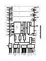
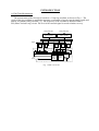
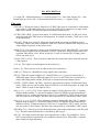
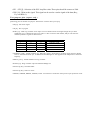
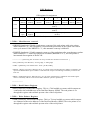
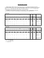
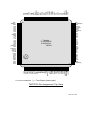
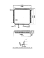
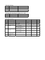
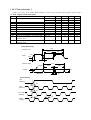
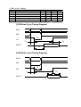
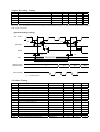
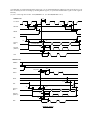
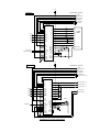
TMC304(TEG3) User's Manual
Yasuo Arai
KEK, National Laboratory for High Energy Physics
1-1 Oho, Tsukuba, Ibaraki 305, Japan
[email protected]
http://www-atlas.kek.jp/~araiy/
Ver 1.5 Jan. 17, 2002
(Chip designed in 1994)
TMC304 (previous name TMCTEG3) is a low-power and high-resolution multi-hit Time to
Digital Converter chip. Input signals are digitized at TMC (Time Memory Cell) circuits in (clock
period)/32 (0.78 ns @40MHz) time bin. The 32 bits of digitized data is then encoded into a hit bit
and 5-bit data, and stored in memories. The memory is dual port memory so write and read can be
performed at the same time and there is no dead time for data conversion. There are 128 words of
dual port memories, and the chip can store 2.56 µs to 12.8 µs data depend on the system clock
frequency.
If user wants to suppress zero data at the output, signal correspond to the hit tag bit can be used as
a strobe signal to next level buffer.
To stabilize the internal delay element, PLL circuit is used. User can select 10 - 50 MHz system
clock (x1 mode) or 2.5 - 12.5 MHz clock (x4 mode). There are 4 Control and Status Registers
(CSR's) which can be read and write from 8 bit CSR bus. TMC304 chip has 4 input channels.
MAIN FEATURES
• Least Time Count
• Time Resolution
• Integral Linearity Error
• Differential Linearity Error
• Stability
• System Clock Frequency
• No. of Channels
• Recording depth
• Double Hit Resolution
• Readout mode
: 0.6 - 3.1 ns/bit
: RMS = 250 ps (@40 MHz)
: < 80 ps @40MHz
: < 60 ps @40MHz
: (3.0 - 3.6 V. 0 - 70 ˚C)
: 10 - 50 MHz (x1 mode)
2.5 - 12.5 MHz (x4 mode)
: 4 Channels
: 128 clock cycle (2.56 - 12.8 µs)
• Data format
• Supply Voltage
• Process
: 25 - 32 ns
: (i) Synchronous read mode (individual channel zero suppress)
(ii) Synchronous read mode (all channel zero suppress)
(iii) Asynchronous read mode (4 channel access)
(iv) Asynchronous read mode (1 channel access)
: dual edge encode (hit tag + 5 bit)
: 3.3 V (3.0 - 3.6V)
: 0.5 µm CMOS Sea-of-Gate
• Power Dissipation
• Package
: ~ 50 mW/Channnel (@40MHz, Input=1MHz)
: 0.5 mm lead pitch, 144 pin plastic QFP
[• Test Circuits
: Ring Oscillator, NMOS and PMOS transistors.]
EDCLK
CLKP
CLKN
ROSC
TSTROSC
DIV4
SF1-2
RESET*
ROOUT
ENRO*
UP,DN
COM
NMOSG,D
PMOSG,D
WTCEN
WTCLK
WSTART
WRUN
RRUN
RSTART
RMOD0-1
RCLK
DCH0
DCH1
RE*
ZSG*
Clock
&
Misc.
Control
Test
Circuit
Write
Control
Read
Control
Output
Control
WS*
6
ED
VGN0
32b RTMC
Latch
F00-04
PLL
F encoder
6
12 bit x 128 word
DPM
T
F05
TMC304(TEG3) Block Diagram
CIO0-7* WR* CS* RA0-1
T
R05 R00-04
R encoder
TIN0P TIN0N
Test&Misc.Reg.
Write Pointer
Read Pointer
CSR I/F
CSR0,3
CSR2
CSR1
RP0-6
TIN1P TIN1N
VGN1
Ch1
TIN2P TIN2N
VGN2
Ch2
1995.11.13 Y.A
TIN3P TIN3N
VGN3
Ch3
R10-15 F10-15 R20-15 F20-15 R30-15 F30-15
INTRODUCTION
A. Fine-Time Measurement
The measurement of the fine time is based on a 32 tap ring oscillator as shown in Fig. 1. The
circuit of the ring oscillator is modified to generate even number of equaly spaced timing signals and
named “Asymmetric Ring Oscilator” [1]. The frequency of the oscillator is stabilized with a
PLL(Phase Locked Loop) circuit. The level of the external signal is stored to latches at every
Rising Edge Data
Falling Edge Data
128W x 6b DPM
128W x 6b DPM
Latch & Encoders
Signal
D Q
D Q
D Q
D Q
D Q
• • •
Asym. Ring Osc.
Phase
Freq.
Detector
Clock
Charge
Pump
PLL circuit
Fig. 1 TMC core circuit.
LPF
VGN
Cvg
PIN DESCRIPTION
[I = Input, DI = Differential Input, O = Normal Output, TO = Three State Output; PU = with
internal pull-up resistor, PD = with internal pull-down resistor, * = negative logic]
TMC pins
• EDCLK [I] : When this signal is High level, CLKP/CLKN pins are connected to a differential
input receiver. When this signal is Low level, the CLKP pin is connected to a single ended
input buffer and the CLKN is disconnected from the internal circuit.
• CLKP,CLKN [DI/I] : System clock inputs. In a differential input mode, CLKP act as a noninverting input and CLKN act as a inverting input. In a single end mode, CLKP pin is used
as the clock input.
• DIV4 [I] : Divide by 4 selection. When this signal is high, the internal oscillation clock is
divided by 4 before the phase comparator of the PLL. Thus the internal clock frequency has
4 times higher frequency of the system clock.
• RESET* [I] : This input pin is used to reset all the internal circuit. When RESET* is asserted,
internal registers and circuit are initialized. The PLL circuit does not be affected in the reset
operation when DIV4 is low. When “divide by 4” mode is selected (DIV4=High), phase
lock is lost at the reset.
• CIO0*~CIO7* [I,TO] : These I/O pins are data lines for control bus which read and write the
CSR registers.
• CS* [I] : This signal is a strobe signal for the control bus.
• RA0~1 [I] : These pins are used as address line to the control bus.
• WR* [I] : This pin is a Read/Write* select signal in the control bus.
• ED [I] : When this signal is High level, TINxP/TINxN (x=0..3) pins are connected to a
differential input receiver. When this signal is Low level, the TINxP pin is connected to a
single ended input buffer and the TINxN pin is disconnected from internal circuit.
• TIN0P ~ TIN3P,TIN0N~3N [DI/I] : Inputs for time measuring signals. In differential input
mode, TINxP act as a non-inverting input and TINxN act as a inverting input. In single end
mode, TINxP is used for the input of clock.
• Rxy (x=0..3, y=0..5) [TO] : These signals are output of rising edge data. The "x" denotes
channel number and the "y" denotes bit number. Bit 0 to 4 indicate encoded data and bit 5
indicates a hit tag. Timing characteristic of the bit 5 is controlled by ZSG* signal, and user
can select pulse or level output. The three-state output buffer is controlled by a RE* signal.
• Fxy (x=0..3, y=0..5) [TO] : These signals are output of falling edge data. The "x" denotes
channel number and the "y" denotes bit number. Bit 0 to 4 indicate encoded data and bit 5
indicates a hit tag. Timing characteristic of the bit 5 is controlled by ZSG* signal, and user
can select pulse or level output. The three-state output buffer is controlled by a RE* signal.
• RP0-RP6 [TO] : These pins provide the Read Pointer value with synchronous to the Rxy and
Fxy. The three-state output buffer is controlled by RE* signal.
• RE* [I] : This input controls the three-state output buffers of Rxy, Fxy and RP0-6. When
RE* is asserted those output buffers are enabled as shown below. When RE* is negated,
those output has high impedance.
RE*
1
0
0
0
0
0
RMODE DCH0, 1
x
x
0, 1, 2
x
3
0
3
1
3
2
3
3
R0y, F0y
Hi Z
enabled
enabled
Hi Z
Hi Z
Hi Z
R1y, F1y
Hi Z
enabled
Hi Z
enabled
Hi Z
Hi Z
R2y, F2y
Hi Z
enabled
Hi Z
Hi Z
enabled
Hi Z
R3y, F3y
Hi Z
enabled
Hi Z
Hi Z
Hi Z
enabled
RP0-RP6
Hi Z
enabled
enabled
enabled
enabled
enabled
• RMOD1~0 [I] : These pins select readout mode as shown below.
RMODE
0
1
2
3
Readout mode
Synchronous read mode (individual channel zero suppress)
Synchronous read mode (all channel zero suppress)
Asynchronous read mode (4 channel access)
Asynchronous read mode (1 channel access)
RMODE = [RMOD1,RMOD0]
RMODE=0 is a synchronous read mode and data will appear at the output at every clock
cycle. Each channel has its own hit tag bit.
RMODE=1 is almost same as the RMODE0 but the R05 indicates ORed signal of all 4
channel hit tag of the rising edge. The F05 indicates ORed signal of all 4 channel hit tag of
the falling edge. In addition, the R15 indicates ORed signal of all 4 channel hit tag of both
rising and falling edge. All other Rx5 signals have same value as in the RMODE=0.
RMODE=2 is an asynchronous read mode, and all 4 channel data are read out
simultaneously controlled by RCLK. In the asynchronous mode, data recording should be
stopped when reading.
RMODE=3 is an asynchronous read mode. In the asynchronous mode, data recording
should be stopped when reading. The data readout is done for each channel selected by
DCH0 and DCH1. Readout timing is controlled by RCLK.
• DCH1~0 [I] : These signals select readout channel when readout mode is 3.
• RCLK [I] : This signal is used to control the data readout timing in the asynchronous read
mode (RMODE=2 or 3).
• ZSG* [I] : This signal controls the timing characteristics of the hit tag outputs (Rx5, Fx5).
When this signal is asserted, the hit tag outputs become pulsed output and can be used to
strobe non-zero data. When this bit is negated, the hit tag outputs has same timing
characteristics as other data line.
• WSTART [I] : This signal starts write cycle of the TMC.
• WRUN [O] : This signal indicates the start of the write cycle in the TMC. This is a
synchronized signal with the system clock.
• RSTART [I] : This signal starts readout cycle of the dual port memory.
• RRUN [O] : This signal indicates the start of the readout cycle of the dual port memory. This
is a synchronized signal with the system clock.
• VGN0-VGN3 [O] : These pins are outputs of PLL loop filter, and must be connected to
external capacitors of ~6800 pF.
• SF1 - SF2 [I] : Selection of the PLL loop filter value.These pins should be connect to Vdd.
• WS* [O] : Write strobe signal. This signal can be used as a strobe signal of the data (Rxy,
Fxy and RP0-6).
Test purpose pins (expert only)
[Following pins are used for test purpose. Normal user can leave those pins open.]
• DN [O] : PLL down signal.
• UP [O] : PLL up signal.
• ROSC [O] : TMC ring oscillator clock output. You can check internal clock signal throgh this pin when
TSTROSC pin is connected to high level. There is a PLL circuit for each channel, and you can select the
channel by DCH0-1 signals as shown below.
TSTROSC
1
1
1
1
0
DCH1
0
0
1
1
x
DCH0
0
1
0
1
x
Ch0
Ch1
Ch2
Ch3
ROSC
PLL Clock
PLL Clock
PLL Clock
PLL Clock
0
• TSTROSC [I, PD] : Enable oscillator test. When this signal is asserted, PLL oscillator output select by DCH0
and 1 is connected to ROSC pin. In addition the selected signal is also supplied to the read pointer to check the
frequency.
• ENRO* [I, PU] : Enable radiation test ring oscillator.
• ROOUT [O] : Ring oscillator output for radiation damage test.
• WTCEN [I, PD] : WTCLK enable.
• WTCLK [I, PD] : Write test clock.
• NMOSG, NMOSD, PMOSG, PMOSD, COM : Test transistor connections. Each pis has input protection circuit.
CSR Registers
CSR registers bit assignment
bit
7
6
5
CSR0
MTEST
(R/W:0)
NRPSYN
(R/W:0)
CSR1
SHIFT
(R/W:0)
0
CSR2
0
CSR3
SOUT
(R:0)
SIN
(R/W:0)
4
3
2
ENRPUP
TCH1
(R/W:0)
(R/W:0)
(R/W:0)
Read Pointer register [RPR]
(R/W:0)
Write Pointer Register [WPR]
(R/W:0)
Test Data Register [TDR]
(R/W:0)
1
0
TCH0
(R/W:0)
F/R*
(R/W:0)
(R/W: x ) --- (Readable/Writeable: Initial value)
* CSR0 : Miscellaneous control.
• NRPSYN [read/write]: Disable synchronous count up of the read pointer with write pointer.
When NRPSYN="0", the read pointer is incremented synchronous to the system clock when
write cycle started. If the NRPSYN="1", this automatic count up is inhibited.
• ENRPUP [read/write] : Enable automatic count up of the read pointer after asynchronous readout.
When ENRPUP="1" and in asynchronous read mode (RMODE=2 or 3), the read pointer is
incremented after negation of the RCLK.
---------------------- [Following bits are used to test chip. Normal user should not set these bits. ]
• F/R* [read/write]: Test data select, =0 rising edge, =1 falling edge.
• TCH0~1 [read/write]: Test channel select. TCH = [TCH1,TCH0].
• MTEST : Memory Test select. When this bit is set, output of the Test Data Register (TDR) is connected to the
input of the DPM and the input of TDR is connected to the output of encoder logic selected by TCH bits and
F/R* bit.
• SHIFT : Enable Shift In/Out. When this bit is set, the value of the SIN bit is shifted into the encode register
which is selected by CH bits at the end of CSR3 read/write operation..[read/write]
------------------------
* CSR1 : Read Pointer Register
• RPR [read/write]: Read Pointer Register. This is a 7-bit loadable up-counter which outputs are
connected to the read addresses of the Dual Port Memory (DPM). The read pointer is set
through this register and read back present value of the read pointer.
* CSR2 : Write Pointer Register
• WPR [read/write]: Write Pointer Register. This is a 7-bit up loadable up-counter which outputs
are connected to the write addresses of the Dual Port Memory (DPM). The write pointer is set
through this register and read back present value of the write pointer.
* CSR3 : Test Data Register
[This register is used to test chip. Normal user should not set this register. ]
• TDR [read/write]: Test Data Register.
• SIN [read/write] : Serial Input bit.
• SOUT [read only] : Serial output bit
Data Encoding Scheme
Digitized data at TMC circuit is encoded before the write operation to the dual port memory.
The data encoding scheme is shown in the following table . Bit position at which the data is changed
from "0" to "1" is encoded in the rising edge data, and bit position of "1" to "0" is encoded in the
falling edge data. Hit tag bit shows the existence of those transition.
In addition to the transition encoding, user can get all "0" or all "1" information by taking the
encoded data at no hit tag. This may help more understanding of the signal behavior.
Rising Edge
row
data
0
0
1
0
x
d
d
:
d
d
1
0
d
1
0
d
d
:
d
d
2
0
d
x
1
0
d
:
d
d
3
0
d
x
x
1
0
:
d
d
4
0
d
x
x
x
1
:
d
d
5
0
d
x
x
x
x
:
d
d
...
•
•
•
•
•
•
:
•
•
•
•
•
•
•
•
:
•
•
...
•
•
•
•
•
•
:
•
•
30
0
d
x
x
x
x
:
0
d
31
0
d
x
x
x
x
:
1
0
next
cycle
0
0
d
x
x
x
x
:
x
1
[Rx5]
Hit
Tag
0
0
1
1
1
1
:
1
1
[Rx4..0]
Comment
Encoded
Data
0
all 0
1
all 1 /no R edge
0
edge at 0-1
1
edge at 1-2
2
edge at 2-3
3
edge at 3-4
:
:
30
edge at 30-31
31
edge at 31-0
31
1
u
x
x
x
x
:
0
1
next
cycle
0
1
u
x
x
x
x
:
x
0
[Fx5]
Hit
Tag
0
0
1
1
1
1
:
1
1
[Fx4..0]
Comment
Encoded
Data
0
all 1
1
all 0 /no F edge
0
edge at 0-1
1
edge at 1-2
2
edge at 2-3
3
edge at 3-4
:
:
30
edge at 30-31
31
edge at 31-0
Falling Edge
row
data
0
1
0
1
x
u
u
:
u
u
1
1
u
0
1
u
u
:
u
u
2
1
u
x
0
1
u
:
u
u
3
1
u
x
x
0
1
:
u
u
d..d = no rising edge
u..u = no falling edge
x = don't care
4
1
u
x
x
x
0
:
u
u
5
1
u
x
x
x
x
:
u
u
...
•
•
•
•
•
•
:
•
•
•
•
•
•
•
•
:
•
•
...
•
•
•
•
•
•
:
•
•
30
1
u
x
x
x
x
:
1
1
TMC304 Pin Assignments
Pin No
1
2
3
4
5
6
7
8
9
10
11
12
13
14
15
16
17
18
19
20
21
22
23
24
25
26
27
28
29
30
31
32
33
34
35
36
Signal Name
VDD
CIO0*
CIO1*
CIO2*
CIO3*
VSS
CIO4*
CIO5*
CIO6*
CIO7*
ZSG*
VSS
R00
R01
R02
R03
R04
VDD
R05
(ROOUT)
WS*
RRUN
TIN0N
TIN0P
TIN1N
TIN1P
VSS
ED
TIN2N
TIN2P
TIN3N
TIN3P
VSS
VDD[PMOSD]
VDD[PMOSG]
(COM)
Pin No Signal Name
37 VSS[NMOSG]
38 VSS[NMOSD]
39 VDD
40 VDD
41 F00
42 F01
43 F02
44 VSS
45 F03
46 F04
47 F05
48 SF1
49 SF2
50 WR*
51 (DN)
52 (UP)
53 VSS
54 CS*
55 DIV4
56 R10
57 R11
58 R12
59 R13
60 VDD
61 R14
62 R15
63 VSS
64 VSS
65 (WTCEN)
66 DCH1
67 DCH0
68 (WTCLK)
69 ROSC
70 VSS
71 (TSTROSC)
72 RE*
)
Pin No
73
74
75
76
77
78
79
80
81
82
83
84
85
86
87
88
89
90
91
92
93
94
95
96
97
98
99
100
101
102
103
104
105
106
107
108
Signal Name
VDD
RMOD0
RMOD1
VSS
F10
F11
F12
F13
VSS
F14
F15
VDD
VGN0
VGN1
VSS
VGN2
VGN3
VDD
R20
R21
VSS
R22
R23
R24
R25
(ENRO*)
RA0
RA1
VSS
F20
F21
VDD
F22
F23
F24
F25
Pin No Signal Name
109 VSS
110 RESET*
111 VDD
112 R30
113 R31
114 R32
115 R33
116 VSS
117 R34
118 R35
119 WRUN
120 VDD
121 F30
122 F31
123 F32
124 F33
125 VSS
126 F34
127 F35
128 VSS
129 RSTART
130 VDD
131 WSTART
132 RCLK
133 EDCLK
134 CLKN
135 CLKP
136 VSS
137 RP0
138 RP1
139 RP2
140 RP3
141 VDD
142 RP4
143 RP5
144 RP6
* --- negative logic
( ) -- Test Signals (leave open)
F25
F24
F23
F22
VDD
F21
F20
VSS
RA1
RA0
(ENRO*)
R25
R24
R23
R22
VSS
R21
R20
VDD
VGN3
VGN2
VSS
VGN1
VGN0
VDD
F15
F14
VSS
F13
F12
F11
F10
VSS
RMOD1
RMOD0
VDD
73
VSS
RESET*
VDD
R30
R31
R32
R33
VSS
R34
R35
WRUN
VDD
F30
F31
F32
F33
VSS
F34
F35
VSS
RSTART
VDD
WSTART
RCLK
EDCLK
CLKN
CLKP
VSS
RP0
RP1
RP2
RP3
VDD
RP4
RP5
RP6
109
Toshiba
TC180G26HS
01019423-xx
JAPAN
37
RE*
(TSTROSC)
VSS
(ROSC)
(WTCLK)
DCH0
DCH1
(WTCEN)
VSS
VSS
R15
R14
VDD
R13
R12
R11
R10
DIV4
CS*
VSS
(UP)
(DN)
WR*
SF2
SF1
F05
F04
F03
VSS
F02
F01
F00
VDD
VDD
(NMOSD)
VSS
VSS
(NMOSG)
VDD
CIO0*
CIO1*
CIO2*
CIO3*
VSS
CIO4*
CIO5*
CIO6*
CIO7*
ZSG*
VSS
R00
R01
R02
R03
R04
VDD
R05
(ROOUT)
WS*
RRUN
TIN0N
TIN0P
TIN1N
TIN1P
VSS
ED
TIN2N
TIN2P
TIN3N
TIN3P
VSS
VDD
(PMOSD)
(PMOSG)
VDD
n.c.
(COM)
1
n.c.=non connection, ( ) = Test Signals (leave open)
TMCTEG3 Pin Assignment (Top View)
95.2.22 Y.Arai
QFP144 Shrink 144-pin Plastic Flat Package (unit : mm)
• Maximum Ratings
Symbol
VDD
VIN
IIN
TSTG
Parameter
DC Supply Voltage
Input Voltage
Input Current
Storage Temperature
Value
-0.3 to +5.0 V
-0.3 to VDD+0.3 V
±10 mA
-40 to +125 ˚C
• Recommended Operating Condition ( VS S = 0V)
Symbol
VDD
Ta
Parameter
DC Supply Voltage
Ambient Temperature
Value
3.0 to 3.6 V
0 to +70 ˚C
• DC Characteristics
Symbol
VIH
VIL
IIH
IIL
VOH
VOL
IOZ
IDDS
Parameter
Input High Voltage
Input Low Voltage
Input High Current
Input Low Current
High-Level Output
Voltage
Low-Level Output
Voltage
3-state Output
Leakage Current
Quiescent Device
Current
Condition
VIN = VDD
VIN = VSS
RRUN, WRUN, ROSC
IOH = -4 mA (B4)
All Signals except above.
IOH = -8 mA (B8)
RRUN, WRUN, ROSC
IOH = 4 mA (B4)
All Signals except above
IOH = 8 mA (B8)
Min
VDD x 0.8
VDD x 0.2
-10
-10
2.4
Unit
10
10
µA
µA
V
2.4
-10
VIN = VDD or VSS
Max
V
0.4
V
0.4
V
10
µA
60
µA
VOH-VDD(V)
-3.0
-2.5
-2.0
-1.5
-1.0
-0.5
0.0
0
-20
-40
B8
-60
-80
Fig.1 Output High Level Current Characteristic
(VDD=3.3V, Ta=25 °C, typ)
80
B8
IOL(mA)
60
B4
40
20
0
0.0
0.5
1.0
1.5
2.0
2.5
VOL(V)
Fig. 2 Output Low Level Current Characteristic
(VDD=3.3V, Ta=25 °C, typ)
3.0
IOH(mA)
B4
[ AC Characteristics ]
( VDD = 3.3 V, Ta = 25 ˚C. ROSC, WRUN, RRUN : Cload = 25 pF, All other output signals : Cload = 50 pF )
• Clock Signal Characteristics
Symbol
f0
Characteristics
CLK frequency
T1
T2L/T2H
Vcenter
∆V
∆V/T3
T4L/T4H
T5
T6
T7
CLK rise and fall time
CLK duty factor
Center voltage of differential clock
Differential clock amplitude
CLK rise and fall rate
CLK duty factor
External clock and PLL clock phase offset
External clock and PLL clock phase offset
Rising edge delay between ROSC output
and PLL clock
Falling edge delay between ROSC output
and PLL clock
T8
Condition
DIV4=L
DIV4=H
EDCLK=L
EDCLK=L
EDCLK=H
EDCLK=H
EDCLK=H
EDCLK=H
DIV4=1
DIV4=0
TSTROSC=1
Min
10
2.5
0.6
1.4
100
0.6
-4
-3
2.5
Typ
1.0
1.0
- 1.7
- 0.7
4.2
Max
50
12.5
3.0
1.4
2.6
1
1.4
1
2
6.3
Unit
MHz
MHz
ns
TSTROSC=1
2.8
4.7
7.1
ns
[Clock Waveforms]
1/f0
• EDCLK=Low
T2H
T2L
2.0V
CLKP
0.8V
T1
T1
• EDCLK=High
1/f0
CLKP
T4L
T4H
Vcenter
DV
T3
CLKN
[Clock Offsets]
CLK
(DIV4=H)
T5
CLK
(DIV4=L)
T6
PLL clock
(internal)
T7
ROSC
(output)
T8
V
mV
V/ns
ns
ns
ns
• CSR Access Timing
Symbol
T1
T2
T3
T4
T5
T6
Characteristics
RA, WR* setup time
RA, WR* hold time
CS* asserted to CIO* asserted
CS* negated to CIO* negated
CIO* setup time
CIO* hold time
Min
1.0
2.0
4.4
2.8
0.0
3.0
Typ
-
Max
12
8
-
Unit
ns
ns
ns
ns
ns
ns
[CSR Read Cycle Timing Diagram]
RA0-1
WR*
T2
CS*
T1
T4
CIO0-7*
T3
[CSR Write Cycle Timing Diagram]
RA0-1
WR*
T2
CS*
T1
CIO0-7*
T5
T6
• Input Recording Timing
Symbol Characteristics
Condition
Min
Typ
Max
Unit
T1
WSTART safety area start timing (*)
1.5
ns
T2
WSTART safety area end timing (*)
0.1
ns
T3
WRUN assert timing
2.8
7.1
ns
T4
WRUN negate timing
2.9
7.3
ns
T5
Input recording timing
∆t=bit width
7∆t
ns
(*) If WSTART is asserted outside of this safety area, it is not guaranteed that the input recording will start from the
next cycle. User can identify the start of recording by checking WRUN signal., or synchronize the WSTART signal to
CLK signal if necessary.
[Input Recording Timing]
(PLL clcok)
T1
T2
T1
T2
WSTART
T3
T4
WRUN
T5
TINx
T5
Data Recording
(Write Pointer)
(Read Pointer)
N
N+1
N+2
N+3
(Write Strobe*)
( ) -- Internal Signal
• Readout Timing
Symbol
T1
T2
T3
T4
T5
T6
T7
T8
T9
T10
T11
T12
T13
T14
T15
T16
Characteristics
RSTART safety area start timing (*)
RSTART safety area end timing (*)
RRUN assert timing
RRUN negate timing
RE* assert to data line enable time
RE* negate to data line disable time
PLL clock high to data assert time
Data change to Rx5, Fx5 assert time
Rx5, Fx5 pulse width (**)
WS* assert to data change time
WS* pulse width (**)
RMOD to RRUN assert time
RCLK high pulse width (=Tch)
RCLK cycle time
RCLK high to data assert time
DCHx to channel data change time
Condition
RMODE=0 or 1
RMODE=0 or 1
RMODE=0 or 1
RMODE=0 or 1
RMODE=0 or 1
ZSG*=L
RMODE=2 or 3
RMODE=2 or 3
RMODE=2 or 3
RMODE=2 or 3
RMODE=3
Min
3.1
2.9
3.4
3.0
3.9
0.8
Tch+0.8
0.8
Tch+0.1
3.1
5
20
4.1
3.7
Max
1.1
0.3
7.8
7.4
9.5
10.2
10.5
3.8
Tch+2.3
3.3
Tch+0.4
7.6
11.6
8.5
Unit
ns
ns
ns
ns
ns
ns
ns
ns
ns
ns
ns
ns
ns
ns
ns
ns
(*) If RSTART is asserted outside of this safety area, it is not guaranteed that the readout will start from the next cycle.
User can identify the start of reading by checking RRUN signal., or synchronize the RSTART signal to CLK signal if
necessary.
(**) Tch : Clock high time of PLL clock(RMODE=0 or 1) or RCLK(RMODE=2 or 3).
Tch
• RMODE=0 & 1
PLL Clock
T1
T2
T1
T2
RSTART
T3
T4
RRUN
RE*
T5
T6
T7
Rxy,Fxy
RPz
previous data
T9
T8
Rx5,Fx5
(ZSG*=L)
T10
T11
WS*
• RMODE=2 & 3
RMODx
RMODE=2 or 3
T12
RRUN
T14
T13 (=Tch)
RCLK
DCHx
T16
RE*
T6
T5
Rxy,Fxy
RPz
T15
previous data
T9
T8
Rx5,Fx5
(ZSG*=L)
T10
WS*
T11
Readout Timing
+3.3V
To Readout Sy s t em
RMODE=0
Reset*
System Clock
CSR Select*
Read/Write*
Address Bus
Data Bus*
TMC304
CIO*
A1
A0
CH3
RA1
RA0
WR*
CS*
TIN3P
TIN3N
TIN2P
TIN2N
TIN1P
TIN1N
TIN0P
TIN0N
ED
CH2
CH1
CH0
CLKP
CLKN
EDCLK
RP
RP
R3
F3
F3
R3
R2
F2
F2
R2
R1
F1
F1
R1
R0
F0
Level2
Buffer
R0
F0
6800pF
VGN3
VGN2
VGN1
VGN0
SF2
SF1
DIV4
WriteStrobe*
ZSG*
WSTART
RSTART
RCLK
DCH1
DCH0
RE*
WS*
RESET
WRUN
RMOD1
RRUN
RMOD0
Write Start
Readout Trigger
+3.3V
RMODE=3
T o Readout Sy st em
Reset*
System Clock
CSR Select*
Read/Write*
Address Bus
Dat a B us ( CIO0 ..7* )
TMC304
CIO*
A1
A0
CH3
RA1
RA0
WR*
CS*
TIN3P
TIN3N
TIN2P
TIN2N
TIN1P
TIN1N
TIN0P
TIN0N
ED
CH2
CH1
CH0
CLKP
CLKN
EDCLK
Write Start
A1
A0
RP
Dat a B us ( RP0.. 6)
R3
Data Bus (R0..5)
F3
Data Bus (F0..5)
R2
F2
Data Read*
R1
Data Strobe
F1
R0
F0
6800pF
VGN3
VGN2
VGN1
VGN0
SF2
SF1
DIV4
ZSG*
WSTART
RSTART
RCLK
DCH1
DCH0
RE*
WS*
RESET
WRUN
RMOD1
RRUN
RMOD0
Exapmles of signal connections.