1
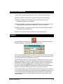
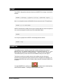
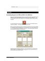
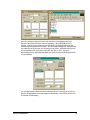
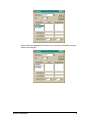
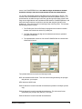
2608 Sweetgum Drive Apex NC 27502 Toll-free: 800-549-9377 International: 919-387-0076 FAX: 919-387-1302 XSTOOLs V4.0 User Manual GUI-Based and Command Line-Based XS Board Utilities RELEASE DATE: 9/21/2001 Copyright ©1997-2001 by X Engineering Software Systems Corporation. All XS-prefix product designations are trademarks of XESS Corp. All XC-prefix product designations are trademarks of Xilinx. All rights reserved. No part of this publication may be reproduced, stored in a retrieval system, or transmitted, in any form or by any means, electronic, mechanical, photocopying, recording, or otherwise, without the prior written permission of the publisher. Printed in the United States of America. XSTOOLS 4.0 USER MANUAL 1 GXSTOOLS Components The XSTOOLs package contains these GUI-based / command line-based utilities: GXSTEST / XSTEST: This utility lets you test an XS Board for proper functioning. GXSSETCLK / XSSETCLK: This utility lets you set the clock frequency of the programmable oscillator on an XS Board. GXSLOAD / XSLOAD: This utility lets you download FPGA and CPLD configuration files and upload/download data files to the RAM and/or Flash on an XS Board. GXSPORT / XSPORT: This utility lets you send logic inputs to an XS Board by toggling the data pins of the PC parallel port. Instructions for using these utilities are presented in the following sections. GXSTEST You start GXSTEST by clicking on the icon placed on the desktop during the XSTOOLS installation. This brings up the window shown below. Next you select the parallel port that your XS Board is connected to from the Port pulldown list. GXSTEST starts with parallel port LPT1 as the default, but you can also select LPT2 or LPT3 depending upon the configuration of your PC. After selecting the parallel port, you select the type of XS Board you are testing from the Board Type pulldown list. Then click on the TEST button to start the testing procedure. GXSTEST will configure the FPGA to perform a test procedure on your XS Board. After several seconds you will see a O displayed on the LED digit if the test completes successfully. Otherwise an E will be displayed if the test fails. A status window will also appear on your PC screen informing you of the success or failure of the test. If your XS Board fails the test, you will be shown a checklist of common causes for failure. If none of these causes applies to your situation, then test the XS Board using another PC. In our experience, 99.9% of all problems are due to the parallel port. If you cannot get your board to pass the test even after taking these steps, then contact XESS Corp for further assistance. XSTOOLS 4.0 USER MANUAL 2 XSTEST The XSTEST utility performs the same functions as GXSTEST, but using a command line interface: XSPORT [-[h|help]] [-[p|port] [1|2|3]] [-[b|board] <type>] Here is an example that tests an XS40-005XL Board connected to the LPT2 parallel port: XSTEST –p 2 –b xs40-005xl XSTEST remembers the parallel port and type of XS Board that was used on the previous run, so the next example re-runs the test on the XS40-005XL Board: XSTEST You can get a synopsis of the XSTEST command arguments as follows: XSTEST -help GXSSETCLK The XS Boards have a 100 MHz programmable oscillator (a Dallas Semiconductor DS1075Z-100). The 100 MHz master frequency can be divided by factors of 1, 2, ... up to 2052 to get clock frequencies of 100 MHz, 50 MHz, ... down to 48.7 KHz, respectively. The divided frequency is sent to the rest of the XS Board circuitry as a clock signal. The divisor is stored in non-volatile memory in the oscillator chip so it will resume operation at its programmed frequency whenever power is applied to the XS Board. You can store a particular divisor into the oscillator chip by using the GUI-based GXSSETCLK as follows. You start GXSSETCLK by clicking on the icon placed on the desktop during the XSTOOLS installation. This brings up the window shown below. XSTOOLS 4.0 USER MANUAL 3 Your next step is to select the parallel port that your XS Board is connected to from the Port pulldown list. GXSSETCLK starts with parallel port LPT1 as the default, but you can also select LPT2 or LPT3 depending upon the configuration of your PC. Then select the type of XS Board from the Board Type pulldown list. Next you enter a divisor between 1 and 2052 into the Divisor text box and then click on the SET button. Then follow the sequence of instructions given by GXSSETCLK for moving shunts and removing and restoring power during the oscillator programming process. At the completion of the process, the new frequency will be programmed into the DS1075. An external clock signal can be substituted for the internal 100 MHz oscillator of the DS1075. Checking the External Clock checkbox will enable this feature in the programmable oscillator chip. If this option is selected, you are then responsible for providing the external clock to the XS Board through an external pin. (Check the manual for your particular XS Board to find the location of the external clock pin.) XSSETCLK The XSSETCLK utility performs the same functions as GXSSETCLK, but using a command line interface: XSSETCLK [-[h|help]] [-[p|port] [1|2|3]] [-[b|board] <type>] [-[d|divisor] <number>] [-[e|external]] Here is an example that sets the oscillator on the XS95-108 Board to 25 MHz (100 MHz / 4 = 25 MHz) through a connection to the LPT1 parallel port: XSSETCLK –p 1 –b xs95-108 –div 4 XSSETCLK remembers the parallel port and type of XS Board that was used on the previous run, so the next example reprograms the oscillator with a divisor of 2 that is applied to an external clock source instead of the internal 100 MHz oscillator: XSSETCLK –div 2 –external You can get a synopsis of the XSSETCLK command arguments as follows: XSTOOLS 4.0 USER MANUAL 4 XSSETCLK -help GXSLOAD Downloading Designs into the FPGA and CPLD of Your XSA Board During the development and testing phases, you will usually connect your XS Board to the parallel port of a PC and download your circuit each time you make changes to it. You can download an FPGA or CPLD design into your XS Board using the GXSLOAD utility as follows. You start GXSLOAD by clicking on the icon placed on the desktop during the XSTOOLS installation. This brings up the window shown below. Next you select the parallel port that your XS Board is connected to from the Port pulldown list. GXSTEST starts with parallel port LPT1 as the default, but you can also select LPT2 or LPT3 depending upon the configuration of your PC. Then select the type of XS Board you are using from the Board Type pulldown list. After setting the board type and parallel port, you can download .BIT or .SVF files to the FPGA or CPLD on your XS Board simply by dragging them to the FPGA/CPLD area of the GXSLOAD window as shown below. XSTOOLS 4.0 USER MANUAL 5 Once you release the left mouse button and drop the file, the highlighted file name appears in the FPGA/CPLD area and the Load button in the GXSLOAD window is enabled. Clicking on the Load button will begin sending the highlighted file to the XS Board through the parallel port connection. .BIT files contain configuration bitstreams that are loaded into the FPGA while .SVF files will go to the CPLD. GXSLOAD will reject any non-downloadable files (ones with a suffix other than .BIT or .SVF). During the downloading process, GXSLOAD will display the name of the file and the progress of the current download. You can drag & drop multiple files into the FPGA/CPLD area. Clicking your mouse on a filename will highlight the name and select it for downloading. Only one file at a time can be selected for downloading. XSTOOLS 4.0 USER MANUAL 6 Double-clicking the highlighted file will deselect it so no file will be downloaded Doing this disables the Load button. XSTOOLS 4.0 USER MANUAL 7 Storing Non-Volatile Designs in Your XSA Board The FPGA on an XS Board stores its configuration in an on-chip SRAM which is erased whenever power is removed. (CPLDs on the XS Boards store their configuration in an internal Flash memory that retains its contents even after power is removed.) Once your design is finished, you may want to store the bitstream in the Flash RAM (for XSA or XSV Boards) or serial EEPROM (for XS40 Boards) on your XS Board. The Flash or EEPROM will configure the FPGA for operation as soon as power is applied. An FPGA .BIT file can be downloaded directly to a serial EEPROM. But before downloading to Flash, the FPGA .BIT file must be converted into a .EXO or .MCS format using one of the following commands: promgen –u 0 file.bit –p exo –s 256 promgen –u 0 file.bit –p mcs –s 256 In the commands shown above, the bitstream in the file.bit file is transformed into an .EXO or .MCS file format starting at address zero and proceeding upward until the upper address limit is reached. (The XSA Board has a 256 KByte Flash while the XSV Boards have a 2 MByte Flash.) Before attempting to program the Flash, you must place all DIP switches on the XSA or XSV Board into the OFF position! The .MCS or .EXO (.BIT) file is loaded into the Flash (EEPROM) device by dragging it into the Flash/EEPROM area and clicking on the Load button. This activates the following sequence of steps: 1. The entire Flash (EEPROM) is erased. 2. The CPLD on the XSA or XSV Board is reprogrammed to create an interface between the Flash device and the PC parallel port. (This FPGA on the XS40 Board is programmed to create an interface between the EEPROM and the PC parallel port.) 3. The contents of the .EXO or .MCS (.BIT) file are downloaded into the Flash (EEPROM) through the parallel port. 4. The CPLD is reprogrammed to create a circuit that configures the FPGA with the contents of the Flash when power is applied to the XSA or XSV Board. (This step is not needed for the XS40 Board.) Multiple files can be stored in the Flash device just by dragging them into the Flash/EEPROM area, highlighting the files to be downloaded and clicking the Load button. (Note that anything previously stored in the Flash will be erased by each new download.) This is useful if you need to store information in the Flash in addition to the FPGA bitstream. Files are selected and de-selected for downloading just by clicking on their XSTOOLS 4.0 USER MANUAL 8 names in the Flash/EEPROM area. The address ranges of the data in each file should not overlap or this will corrupt the data stored in the Flash device! You can also examine the contents of the Flash device by uploading it to the PC. (The contents of the serial EEPROM on the XS40 Board cannot be uploaded to the PC.) To upload data from an address range in the Flash, type the upper and lower bounds of the range into the High Address and Low Address fields below the Flash/EEPROM area, and select the format in which you would like to store the data using the Upload Format pulldown list. Then click on the file icon and drag & drop it into any folder. This activates the following sequence of steps: 1. The CPLD on the XSA or XSV Board is reprogrammed to create an interface between the Flash device and the PC parallel port. 2. The Flash data between the high and low addresses (inclusive) is uploaded through the parallel port. 3. The uploaded data is stored in a file named FLSHUPLD with an extension that reflects the file format. The uploaded data can be stored in the following formats: MCS: Intel hexadecimal file format. This is the same format generated by the promgen utility with the –p mcs option. HEX: Identical to MCS format. EXO-16: Motorola S-record format with 16-bit addresses (suitable for 64 KByte uploads only). EXO-24: Motorola S-record format with 24-bit addresses. This is the same format generated by the promgen utility with the –p exo option. EXO-32: Motorola S-record format with 32-bit addresses. XSTOOLS 4.0 USER MANUAL 9 XESS-16: XESS hexadecimal format with 16-bit addresses. (This is a simplified file format that does not use checksums.) XESS-24: XESS hexadecimal format with 24-bit addresses. XESS-32: XESS hexadecimal format with 32-bit addresses. After the data is uploaded from the Flash, the CPLD on the XSA or XSV Board is left with the Flash interface programmed into it. You will need to reprogram the CPLD with either the parallel port or Flash configuration circuit before the board will function again. Check the manual for your particular board for details on this. Downloading and Uploading Data to/from the RAM in Your XS Board The XS Boards contain various amounts of RAM whose contents can be downloaded and uploaded by GXSLOAD. This is useful for initializing the RAM with data for use by the FPGA or CPLD and then reading the RAM contents after the FPGA or CPLD has operated upon it. The RAM is loaded with data by dragging & dropping one or more .EXO, .MCS, .HEX, and/or .XES files into the RAM area of the GXSLOAD window and then clicking on the Load button. This activates the following sequence of steps: 1. The FPGA or CPLD on the XS Board is reprogrammed to create an interface between the RAM device and the PC parallel port. 2. The contents of the .EXO, .MCS, .HEX or .XES files are downloaded into the RAM through the parallel port. The data in the files will overwrite each other if their address ranges overlap. 3. After the data is downloaded to the RAM, any highlighted bitstream file in the FPGA/CPLD area is downloaded into the FPGA or CPLD on the XS Board. Otherwise the FPGA remains configured as an interface to the RAM. You can also examine the contents of the RAM device by uploading it to the PC. To upload data from an address range in the RAM, type the upper and lower bounds of the range into the High Address and Low Address fields below the RAM area, and select the format in which you would like to store the data using the Upload Format pulldown list. Then click on the file icon and drag & drop it into any folder. This activates the following sequence of steps: 1. The FPGA or CPLD on the XS Board is reprogrammed to create an interface between the RAM device and the PC parallel port. 2. The RAM data between the high and low addresses (inclusive) is uploaded through the parallel port. 3. The uploaded data is stored in a file named RAMUPLD with an extension that reflects the file format. XSTOOLS 4.0 USER MANUAL 10 XSLOAD The XSLOAD utility performs the same functions as GXSLOAD, but using a command line interface: XSLOAD [-[h|help]] [-[p|port] [1|2|3]] [-[b|board] <type>] [-[fpga|cpld] <files>] [-ram <files>] [-[flash|seeprom] <files>] [-[u|upload] <lo> <hi>] [-[f|format] [hex|mcs|exo-[16|24|32]|xess-[16|24|32]]] Here is an example that downloads an SVF file to the CPLD on an XSV-300 Board attached to parallel port LPT2: XSLOAD –p 2 –b xsv-300 –cpld dwnldpar.svf XSLOAD remembers the parallel port and type of XS Board that was used on the previous run, so the next example programs the XCV300 Virtex FPGA with a bitstream file: XSLOAD –fpga test.bit A bitstream can be programmed into the Flash using the following sequence of commands. The first command transforms the .BIT file into a Motorola .EXO file. Then the .EXO file is programmed into the Flash on the XSV Board and the CPLD on the XSV Board is reprogrammed such that it will configure the XCV300 FPGA from the Flash on power-up: XSTOOLS 4.0 USER MANUAL 11 promgen –u 0 test.bit –p exo –s 2048 XSLOAD –flash test.exo The contents of the 2 MByte Flash can be verified by uploading the data in an .EXO format (with 24-bit addresses) into a file called chkflash.exo. XSLOAD –flash chkflash.exo –format exo-24 –upload 0 0x1FFFFF Equivalent operations can be performed to download and upload the contents of the RAM: XSLOAD –ram data.hex XSLOAD –ram chkram.hex –format hex –upload 0 0x1FFFFF You can get a synopsis of the XSLOAD command arguments as follows: XSLOAD -help GXSPORT Once you have loaded the XS Board with a configuration file using GXSLOAD, you can then use GXSPORT to exercise the functions of your design. Click on the to bring up the window shown below. icon The window contains several controls which perform the following functions: The Port pulldown list lets you select the parallel port that your XS Board is connected to just like you did with the GXSLOAD program. There are eight buttons, each of which is associated with one of the eight data bits of the parallel port. On startup, each button is labeled with the binary value currently XSTOOLS 4.0 USER MANUAL 12 output on the associated data pin. When you click one of these buttons, the displayed binary value toggles but this new value does not appear on the data pin until you press the Strobe button (see below). The Strobe button transfers the bit values displayed on the data button to the data pins of the parallel port. The Strobe button is enabled if at least one value on a data button is different from the actual value output on its data pin. The Strobe button is disabled if the value on each data pin matches the value on its associated button, because then there is no need to transfer the values. If you check the Count box, the value output on the data pins will increment every time you click on the Strobe button. In this case, the Strobe button will stay enabled. Clicking the Exit button terminates GXSPORT without updating the data pins with any new values that may have been entered. XSPORT The XSPORT utility performs the same functions as GXSPORT, but using a command line interface: XSPORT [-[h|help]] [-[p|port] [1|2|3]] <binary number> Here is an example that outputs the binary value 00001111 on the LPT2 parallel port: XSPORT –p 2 00001111 XSPORT remembers the parallel port that was used on the previous run, so the following example outputs the value 101 on the lower three bits of the LPT2 parallel port: XSPORT 101 You can get a synopsis of the XSPORT command arguments as follows: XSPORT -help XS Board Information File All the XSTOOLs utilities get their information about the various types of XS Boards from the XSBRDINF.TXT file in the top-level installation folder. All blank lines and lines starting with the # character are ignored. The remaining lines contain ten fields separated by one or more whitespace characters. The ten fields have the following meanings: XSTOOLS 4.0 USER MANUAL 13 Field 1 stores the type name of the XS Board. Field 2 stores the identifier of the type of FPGA or CPLD in the XS Board. Field 3 stores the file name of the bitstream file that is loaded into the XS Board to create an interface between the parallel port and the RAM. Field 4 stores the file name of the bitstream file that is loaded into the XS Board to create an interface between the parallel port and the programmable oscillator. Field 5 stores the file name of the bitstream file that erases the interface circuit between the XS Board and the parallel port. Field 6 stores the file name of the bitstream file that is loaded into the XS Board to create an interface between the parallel port and the Flash or serial EEPROM device. Field 7 stores the file name of the bitstream file that is loaded into the XS Board to enable the configuration of the FPGA from the Flash device on power-up. Field 8 stores the file name of the bistream field that is loaded into the interface CPLD of the XS Board to allow testing of the board. Field 9 stores the file name of the bitstream file that is loaded into the FPGA of the XS Board to perform board tests. Field 10 stores the file name of the data file that is loaded into the RAM of the XS Board before testing begins. XSTOOLS 4.0 USER MANUAL 14