1
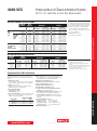
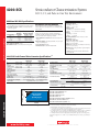
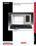
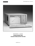
4200-SCS Semiconductor Characterization System The easy-to-use Model 4200-SCS Semiconductor Characterization System performs lab grade DC I-V, C-V, and pulse device characterization, real-time plotting, and analysis with high precision and subfemtoamp resolution. The 4200-SCS offers the most advanced capabilities available in a fully integrated characterization system, including a complete, embedded PC with Windows operating system and mass storage. Its self-documenting, point-and-click interface speeds and simplifies the process of taking data, so users can begin analyzing their results sooner. Additional features enable stress-measure capabilities suitable for a variety of reliability tests. The powerful test library management tools included allow standardizing test methods and extractions to ensure consistent test results. The Model 4200-SCS offers tremendous flexibility with hardware options that include four different switch matrix configurations and a variety of LCR meters and pulse generators. Customer support packages are also available, including applications support, calibration, repair, and training. • Unique Remote PreAmps extend the resolution of SMUs to 0.1fA • C-V instrument makes C-V measurements as easy as DC I-V • Pulse and pulse I-V capabilities for advanced semiconductor testing • Scope card provides integrated scope and pulse measure functionality • Self-contained PC provides fast test setup, powerful data analysis, graphing and printing, and on-board mass storage of test results • Unique browser-style Project Navigator organizes tests by device type, allows access to multiple tests, and provides test sequencing and looping control • Built-in stress/measure, looping, and data analysis for point-and-click reliability testing, including five JEDECcompliant sample tests • Integrated support for a variety of LCR meters, Keithley switch matrix configurations, and both Keithley Series 3400 and Agilent 81110 pulse generators • Includes software drivers for leading analytical probers w w w.keithley.com Applications Packages By combining specific sets of hardware with Keithley-developed code and interconnect, a variety of application packages are offered that expand the Model 4200-SCS’s pulsed testing capabilities. The 4200-PIV-A package performs charge trapping and isothermal testing for leading-edge CMOS research. The 4200-PIV-Q package is designed for higher power pulse testing in III-V, LDMOS, and other higher frequency and higher power FET devices. The 4200-FLASH package tests floating gate FLASH and embedded NVM memory. Extended Measurement Resolution An optional Remote PreAmp, the Model 4200-PA, extends the system’s measurement resolution from 100fA to 0.1fA by effectively adding five current ranges to either SMU model. The PreAmp module is fully integrated with the system; to the user, the SMU simply appears to have additional measurement resolution available. The Remote PreAmp is shipped installed on the back panel of the Model 4200-SCS for local operation. This installation allows for standard cabling to a prober, test fixture, or switch matrix. Users can remove the PreAmp from the back panel and place it in a remote location (such as in a light-tight enclosure or on the prober platen) to eliminate measurement problems due to long cables. Platen mounts and triax panel mount accessories are available. KTE Interactive Software Tools KTE Interactive includes four software tools for operating and maintaining the Model 4200-SCS in addition to the Windows operating system: • The Keithley Interactive Test Environment (KITE) is the Model 4200-SCS Windows device characterization application. It provides advanced test definition, parameter analysis and graphing, and automation capabilities required for modern semiconductor characterization. Built-in looping, stress-measure capabilities, and data management enable many types of reliability testing. A G R E A T E R M E A S U R E O F C O N F I D E N C E SEMICONDUCTOR • Intuitive, point-and-click Windows®-based environment A Total System Solution The Model 4200-SCS provides a total system solution for DC I-V, C-V, and pulse characterization and reliability testing of semiconductor devices, test structures, and materials. This advanced parameter analyzer provides intuitive and sophisticated capabilities for a wide variety of semiconductor tests. The Model 4200-SCS combines unprecedented measurement speed and accuracy with an embedded Windows-based PC and the Keithley Interactive Test Environment (KITE) to provide a powerful singlebox solution. KITE allows users to gain familiarity quickly with tasks such as managing tests and results and generating reports. Sophisticated and simple test sequencing and external instrument drivers simplify performing automated device and wafer testing with combined I-V, C-V, and pulse measurements. The exceptional low current performance of the Model 4200-SCS makes it the perfect solution for research studies of single electron transistors (SETs), molecular electronic devices, and other nanoelectronic devices that require I-V characterization. The Model 4200-SCS can be used to make four-probe van der Pauw resistivity and Hall voltage measurements, eliminating the need for a switch matrix and user-written code. With remote preamps added, resistances well above 1012Ω can be measured. The Model 4200-SCS is modular and configurable. The system supports up to nine Source-Measure Units (SMUs) in any combination of medium and high power SMUs. A high-power SMU provides 1A/20W capability. Also available are the C-V option and the pulse and scope pulse measure modules. The C-V option includes the C-V Power package, which supports high power C-V measurements up to 400V and 300mA, up to 60V of differential DC bias, and quasistatic C-V measurements. Lab grade DC Side device Text characterization DC I-V, C-V, and Pulse in One Test Environment 4200-SCS Semiconductor Characterization System DC I-V, C-V, and Pulse in One Test Environment The Keithley Interactive Test Environment (KITE) is designed to let users understand device behavior quickly. When running a test sequence, users can view results and plots for completed tests while the sequence is still running. As shown here, multiple plots can be viewed at the same time to get a complete picture of device performance. Ordering Information 4200-SCS/F Flat Panel Display Lab grade DC Side device Text characterization 4200-SCS/C Composite Front Bezel; requires an external SVGA display Accessories Supplied Reference and User Manual on CD-ROM 236-ILC-3 Interlock Cable, 3m Note: All 4200-SCS systems and instrument options are supplied with required cables of 2m length. Additional Instrumentation 4210-CVU Integrated C-V Instrument 4205-PG2 Dual-Channel Pulse Generator 4200-SCP2 Dual-Channel Digital Oscilloscope 4200-SCP2HR High Resolution, Dual Channel Integrated Oscilloscope 4200-PIV-A Complete Pulse I-V Package for leading edge CMOS 4200-PIV-Q Pulse I-V Package with Q point and dual-channel pulsing 4200-FLASH Non-volatile Memory Test Package 4200-SCP2-ACC Optional Scope Probe SEMICONDUCTOR Related Products 707A Semiconductor Switching Matrix Mainframe 708A Single Slot Switching Matrix Mainframe 4200-SCP2-ACC 70MHz Scope Probe 7072 8×12 Semiconductor Matrix Card 7072-HV 8×12 High Voltage Semiconductor Matrix Card 7174A 8×12 High Speed, Low Current Matrix w w w.keithley.com • Keithley User Library Tool (KULT)—Allows test engineers to integrate custom algorithms into KITE using Model 4200-SCS or external instruments. • Keithley Configuration Utility (KCON)—Allows test engineers to define the configuration of GPIB instruments, switch matrices, and analytical probers connected to the Model 4200-SCS. It also provides system diagnostics functions. • Keithley External Control Interface (KXCI)—The Model 4200-SCS application for controlling the Model 4200-SCS from an external computer via the GPIB bus. KITE Projects A project is a collection of related tests, organized in a hierarchy that parallels the physical layout of the devices on a wafer. KITE operates on projects using an interface called the project navigator. The project navigator simplifies organizing test files, test execution, and test sequencing. The project navigator organizes tests into a logical hierarchy presented in a browser style format. This structure allows users to define projects around wafer testing: • The project level organizes subsites and controls wafer looping execution. • The subsite level organizes devices and controls subsite test sequencing. • The device level organizes test modules, manages test module libraries, and controls device test sequencing. • The test module level performs tests, analyzes data, and plots results. Prober Control Keithley provides integrated prober control for supported analytical probers when test sequencing is executed on a user-programmable number of probe sites on a wafer. Contact the factory for a list of supported analytical probers. A manual prober mode prompts the operator to perform prober operations during the test sequence. Test Sequencing KITE provides “point and click” test sequencing on a device, a group of devices (subsite, module, or test element group), or a user-programmable number of probe sites on a wafer. One sequence can include DC I-V, C-V, and pulse tests. Keithley User Library Tool (KULT) The Keithley User Library Tool is an open environment that provides you with the flexibility to create your own custom routines as well as use existing Keithley and third-party C-language subroutine libraries. User library modules are accessed in KITE through User Test Modules. Factory supplied libraries provide up and running capability for supported instruments. Users can edit and compile subroutines, then integrate libraries of subroutines with KITE, allowing the Model 4200-SCS to control an entire test rack from a single user interface. KULT is derived from the Keithley S600 and Series S400 Parametric Test Systems. This simplifies migration of test libraries between the Model 4200-SCS and Keithley parametric test systems. A G R E A T E R M E A S U R E O F C O N F I D E N C E 4200-SCS Semiconductor Characterization System DC I-V, C-V, and Pulse in One Test Environment 4210-CVU: Selected C-V Specifications 4210-CVU C-V Instrument C-V measurements are as easy to perform as I-V measurements with the integrated C-V instrument. This optional capacitance-voltage instrument performs capacitance measurements from femtoFarads (fF) to nanoFards (nF) at frequencies from 1kHz to 10MHz. The C-V option includes a new Power package that supports: Measurement Functions Measurement parameters: Cp-G, Cp-D, Cs-Rs, Cs-D, R-jX, Z-theta. Ranging: Auto and fixed. Frequency range: 1kHz to 10MHz. Source Frequency Accuracy: ±0.1%. Signal output level Range: 10mV rms to 100mV rms. Resolution: 1mV rms. Accuracy: ±(10.0% + 1mV rms) unloaded (at rear panel). • High power C-V measurements up to 400V (200V per device terminal)—for testing high power devices, such as MEMs, LDMOS devices, displays, etc. • DC currents up to 300mA—for measuring capacitance when a transistor is on. DC Bias Function DC voltage bias Range: ±30V on both C-V HI and C-V LO (±60V differential). Resolution: 1.0mV. Accuracy: ±(0.5% + 5.0mV) unloaded. Maximum DC Current: 10mA. The innovative design of the 4200-SCS has eight patents pending and is complemented by the broadest C-V test and analysis library available in any commercial C-V measurement solution. It also supplies diagnostic tools that ensure the validity of your C-V test results. Sweep Characteristics With this system, you can configure linear or custom C-V and C-f sweeps with up to 4096 data points. In addition, through the open environment of the 4200-SCS, you can modify any of the included tests, such as: Available sweep parameters: DC bias voltage, frequency, AC drive level. Sweep type: Linear, Custom. Sweep direction: Up sweep, Down sweep. Number of measurement points: 4096 points. • C-V, C-t, and C-f measurements and analysis of: C-V Power Package Typical Performance Characteristics – New! Complete solar cell libraries, including DLCP Measurement Parameters: Cp-Gp, DCV, timestamp. Ranging: 1pF to 1nF. Measurement Terminals: 2-wire SMA, with BNC adapters. Test Signal: 100kHz to 10MHz, 10mV to 100mV. DC Voltage Source: ±200V with 5mV resolution (±400V differential). DC Current: 100mA or 300mA maximum. Typical Cp Accuracy @ 1MHz: 1.0%. DC Current Sensitivity: 10nA/V. SMU Bias Terminals Supported: 4. – High and low k structures – MOSFETs – BJTs – Diodes – III-V compound devices – Carbon nanotube (CNT) devices Lab grade DC Side device Text characterization Test Signal Ramp Rate Quasistatic C-V Typical Performance Characteristics • Doping profiles, TOX, and carrier lifetime tests • Junction, pin-to-pin, and interconnect capacitance measurements Measurement Parameters: Cp, DCV, timestamp. Ranging: 1pF to 1nF. Measurement Terminals: Triaxial guarded. Ramp Rate: 0.1V/s to 1V/s. DC Voltage: ±200V. Typical Cp Accuracy: 5% at 1V/s ramp rate. SEMICONDUCTOR The C-V instrument integrates directly into the Model 4200-SCS chassis. It can be purchased as an upgrade to existing systems or as an option for new systems. w w w.keithley.com A G R E A T E R M E A S U R E O F C O N F I D E N C E 4200-SCS Semiconductor Characterization System DC I-V, C-V, and Pulse in One Test Environment Lab grade DC Side device Text characterization Dual-Channel Pulse Generator The optional, integrated dual-channel pulse generator adds pulsing to the Model 4200-SCS’s DC source and measure capabilities. It supports voltage pulses as short as 10ns or up to ±20V (into 50Ω). Two pulse generators on one card provides you with the flexibility to apply pulses to two points on a DUT, such as the gate and the drain, simultaneously. The 4200-SCS can support up to four synchronized cards per system for eight pulse channels. The 4205-PG2 supports two waveform generation modes in addition to the standard pulse mode. The Arbitrary Waveform mode can generate complex waveforms made up of up to 256K data points at clock speeds up to 25MHz. The Segment ARB™ mode (patent pending) simplifies creating, storing, and generating complex waveforms made from up to 1024 userdefined line segments. Each segment can have a different duration, allowing exceptional waveform generation flexibility. Using a supplied User Test Module, it is simple to incorporate pulse generation into KITE test sequences. The pulse generator can also be used as a stand-alone pulse generator using the pulse generator’s Window’s GUI. This GUI can control a wide range of variables, including pulse frequency, duty cycle, rise/fall time, amplitude, offset, and the ability to trigger single pulses and/or pulse chains. Key Pulse Generator SPECIFICATIONS The dual-channel pulse generator has a wide range of uses. Typical applications Frequency Range 1Hz–50MHz include: Programmable from 10ns to near DC Pulse Width • Charge pumping to characterize interDual independent channels Channels face state densities in MOSFET devices Pulse Amplitude 100mV–20V into 50Ω, 100mV–40V into 1MΩ Range • Using AC stress pulses of varying frequencies to simulate real-world Pulse width, duty cycle, rise time, Programmable fall time, amplitude, offset Parameters AC signals applied to clocked devices • Basic clock generation for test vectoring and failure analysis • Digital triggering The pulse generator can be purchased as an upgrade to existing systems (KTEI version 6.0 or above required) or as an option for new systems. Dual-Channel Digital Oscilloscope The optional dual-channel digital oscilloscopes place more than the performance of a bench-top oscilloscope into your 4200-SCS. They also support time-domain measurements of pulse waveforms and monitor the reactions of devices under test to those pulses. Some of the features of these oscillo scopes include: a broad selection of acquisition modes, triggers, measurements, calculations, and up to four reference waveforms. SEMICONDUCTOR The dual-channel oscilloscopes integrate directly into the Model 4200-SCS chassis. Either can be purchased as an upgrade to existing systems (KTEI version 6.0 or above required) or as an option for new systems. Key Oscilloscope SPECIFICATIONS Bandwidth Channels Maximum Sample Rate w w w.keithley.com 4200-SCP2 4200-SCP2HR (High Resolution) DC to 750MHz DC to 250MHz 2 2 1.25GS/s per channel 200MS/s per channel A G R E A T E R M E A S U R E O F C O N F I D E N C E 4200-SCS Semiconductor Characterization System DC I-V, C-V, and Pulse in One Test Environment 1-year factory warranty extended to 3 years from date of shipment 4200-3Y-CAL 3 (Z540-1 compliant) calibrations within 3 years of purchase for Model 4200-SCS* 4200-FLASH-3Y-EW 1-year factory warranty extended to 3 years from date of shipment 4200-FLASH-3Y-CAL 3 (Z540-1 compliant) calibrations within 3 years of purchase for Model 4200-FLASH* 4200-PA-3Y-EW 1-year factory warranty extended to 3 years from date of shipment 4200-PIV-A-3Y-EW 1-year factory warranty extended to 3 years from date of shipment 4200-PIV-A-3Y-CAL 3 (Z540-1 compliant) calibrations within 3 years of purchase for Model 4200-PIV-A* 4200-PIV-Q-3Y-EW 1-year factory warranty extended to 3 years from date of shipment 4200-PIV-Q-3Y-CAL 3 (Z540-1 compliant) calibrations within 3 years of purchase for Model 4200-PIV-Q* 4200-SCP2-3Y-EW 1-year factory warranty extended to 3 years from date of shipment 4200-SCP2-3Y-CAL 3 (Z540-1 compliant) calibrations within 3 years of purchase for Model 4200-SCP2* 4205-PG2-3Y-EW 1-year factory warranty extended to 3 years from date of shipment 4205-PG2-3Y-CAL 3 (Z540-1 compliant) calibrations within 3 years of purchase for Model 4205-PG2* IMPL-4200 1-day on-site implementation of TRN-42001-C TRN-4200-1-C Course: Optimizing the 4200-SCS for Your Application *Not available in all countries Application Packages Optional application packages combine specific sets of hardware, interconnect, and Keithley developed code. They are described in the following pages. Application packages designed for specific needs 4200-PIV-A For charge trapping and isothermal testing in lower technologies such as CMOS Device FET 4200-PIV-Q For higher power pulse testing in III-V, LDMOS, and other higher frequency and higher power FET devices HEMT, FET Technology Advanced CMOS III-V/LDMOS Source Method Pulse gate, DC bias on drain Measure Method Pulse I-V and DC Measurements Gate voltage, Drain voltage and current Pulse Width Range1 Unique Capability 40ns to 150ns Description 8-bit, 1 gigasample/s measure rate, good for advanced CMOS Pulse I-V testing and high speed single-pulse charge trapping 4200-FLASH For testing FLASH memory devices (NOR and NAND, including MLC technologies) Floating gate FET NAND, NOR, nonvolatile memory Dual pulse for gate and Pulse gate, drain, drain with quiescent source, and substrate point testing Pulse I-V and DC DC only Gate voltage and current, Drain voltage and current 500ns to 999ms Gate voltage and current, Drain voltage and current 250ns to 1s Dual-channel, quiescent point pulsing for scaled-down RF transistors One multi-level pulse channel per DUT pin, integrated High Endurance Output Relay supports endurance testing of NAND and NOR Lab grade DC Side device Text characterization Services Available 4200-3Y-EW SEMICONDUCTOR 1. Full Width Half Maximum (FWHM) w w w.keithley.com A G R E A T E R M E A S U R E O F C O N F I D E N C E 4200-SCS Semiconductor Characterization System DC I-V, C-V, and Pulse in One Test Environment 4200-PIV-A: Pulse I-V Solution Package The 4200-PIV-A Pulse I-V package provides a turnkey pulse I-V solution. It is a comprehensive package of hardware and software, designed to integrate seamlessly with the Model 4200-SCS workstation. It combines the dual-channel pulse generator, dual-channel digital oscilloscope, specialized interconnect, and patented Pulse I-V software. Lab grade DC Side device Text characterization Poly Si Gate Electrode Upper Interfacial Region High κ Film Lower Interfacial Region Bulk Si Pulse I-V measurement capabilities are increasingly critical for high κ gate stack characterization and isothermal testing of new devices. The Pulse I-V software controls sourcing (from the pulse generator) and data acquisition (from the oscilloscope) to automate a variety of Pulse I-V tests. Running in the Model 4200-SCS’s proven interface, the Pulse I-V software provides instrument setup and control, data storage, and presentation. The innovative software includes both cable compensation and a solution to the load-line effect, producing pulsed-based I-V transistor curves, such as the V DS-ID family of curves and VGS-ID for voltage threshold extraction. The Pulse I-V bundle allows the Model 4200-SCS to support a wide range of applications, such as charge trapping for high κ dielectric characterization, isothermal testing of devices and materials subject to self-heating effects, charge pumping, AC stress testing, clock generation, and mixed signal device testing. The specialized interconnect solves most of the problems encountered in high speed pulse testing, such as: DC Source • Combining pulse and DC sources to a single DUT pin to permit both DC and pulse characterization without recabling or switching DC DC Source • Impedance matching for pulse integrity to minimize reflection SEMICONDUCTOR To minimize the signal reflections due to poor impedance matching that often plague “doit-yourself” pulse testing systems, Keithley’s Pulse I-V package includes a system interconnect setup that provides AC/DC coupling to connect the pulse generator and the DC instrumentation. • Straightforward cabling and connection to the DUT for easy setup DC Trigger NEW! 4200-MMPC-X Multi-Measurement Cable Set allows easy changeover from I-V to C-V to PIV AC+DC Out Dual-Channel Pulse Generator The Pulse I-V package includes everything needed to implement a turnkey system for pulsed I-V testing of leading-edge devices and materials. Pieces included in the package are: • Integrated dual-channel pulse generator • Dual-channel digital oscilloscope • Pulse I-V control software (patent pending) • Interconnect designed to minimize the signal reflections common to pulse I-V testing (patent pending) • All required connectors and cables • Sample projects for: - Pulse I-V isothermal testing of FinFETs, SOI devices, and other devices with self-heating problems - Charge-trap testing for high κ gate stack characterization Pulse testing can characterize a device with little to no isothermal degradation. w w w.keithley.com Dual-Channel Digital Oscilloscope for Measurement AC+DC Out A G R E A T E R M E A S U R E O F C O N F I D E N C E 4200-SCS Semiconductor Characterization System DC I-V, C-V, and Pulse in One Test Environment 4200-PIV-Q: Pulsed I-V, Q Point, Dual-Channel, Pulsing Package 4200-FLASH: Non-Volatile Memory Test Package The optional 4200-FLASH application package tests single FLASH memory cells or small arrays quickly and easily using four (or up to eight optional) independent, but synchronized, multi-level pulse channels. It includes all the code and interconnect needed to perform a standard set of FLASH memory tests for NAND and NOR technologies, such as characterization, endurance, and disturb tests. It also supplies the higher pulse voltages that are important for MLC technologies. The 4200-PIV-Q package is designed for quiescent point pulsing of scaleddown RF transistors, such as HEMT and FET devices in III-V or LDMOS technologies. It can be used for a variety of large signal tests on high frequency transistors as well as for investigation of dispersion phenomena and device performance at speed. This package includes multiple 4205-PG2 pulse generators and the 4200-SCP2HR oscilloscope and offers capabilities such as dual-channel pulsing (for pulsing on both the gate and the drain simultaneously), higher power pulsing than the 4200-PIV-A package, and pulsing from a non-zero quiescent point. Some of its features include: • Elimination or characterization of thermal issues • Dual-channel pulse I-V testing for III-V and LDMOS: • Ability to compare DC vs. Pulse for dispersion effects – Pulse voltage on gate and drain • Software and interconnect for Quiescent point testing – Measure gate current, drain voltage, and current • Test code for typical characterization tests – ±20V pulses for the gate, ±38V pulses for the drain • Pulse widths adjustable from 500ns to near-DC (999ms) • Ability to use the same setup for performing true DC tests without re-cabling the system 4200-FLASH takes advantage of the new patent-pending Segment ARB™ waveform generator, which makes typical FLASH program/erase cycles simple to set up and run on a single pulse channel. It also combines the Segment ARB waveform generator with the in-line high endurance relay for Endurance tests. The tight control of this output relay can shorten lifetime test times significantly. 4200-FLASH provides four (or up to Other 4200-FLASH features eight optional) channels of multiinclude: level pulse that support: • Code for performing tests on • ±40V pulsing into a high impefloating gate FLASH and embeddance pin (±20V into 50Ω) ded NVM memory • High endurance output relay • Performs linear or log-based DC which provides fast open/close measurements for Disturb and for pin isolation during an erase Endurance tests based on the pulse number of program/erase cycles • Pulse widths from 200ns to 1s • Controls switching between program/erase and DC charac• Up to 25 pulse levels (100 pulse terization without using a switch segments) matrix • Full support for multi-level cell NEW! 4200-MMPC-X Multi-Measurement Cable Set technology with up to ±40V allows easy changeover from pulsing on the gate I-V to C-V to PIV • Solid state relays with high endurance output relay (HEOR) capability for pin disconnect within Program+Erase waveform Some of the specific tests are: • V DS–ID: Both pulse and DC • VGS–ID: Both pulse and DC • Single-pulse scope view, which is useful for setup validation, pulse width optimization, and prototyping of novel pulse tests w w w.keithley.com A G R E A T E R M E A S U R E O F C O N F I D E N C E SEMICONDUCTOR Typical NOR FLASH gate program/erase cycle Lab grade DC Side device Text characterization Easy setup for program/erase cycles 4200-SCS Semiconductor Characterization System DC I-V, C-V, and Pulse in One Test Environment OPTIONAL APPLICATION PACKAGES 4200-PIV-A Complete Pulse I-V Package for leading edge CMOS 4200-PIV-Q Pulse I-V Package with Q point and dual-channel pulsing 4200-FLASH Non-volatile Memory Test Package OPTIONAL SWITCHING SYSTEMS AND CARDS Systems 707A 6-Slot Switching Matrix Mainframe 708A Single-Slot Switching Matrix Mainframe Cards 7071 7071-4 7072 7072-HV 7075 7173-50 7174A 8×12, General Purpose, Matrix Card Dual 4×12, General Purpose, Matrix Card 8×12, Semiconductor Matrix Card 8×12, High Voltage, Semiconductor Matrix Card Eight 1×12, Two-Pole, Multiplexer Card 4×12, Two-Pole, High Frequency, Matrix Card 8×12, High Speed, Low Leakage Current, Matrix Card SEMICONDUCTOR Lab grade Model DC Side device specifications Text characterization Optional Instrumentation and Accessories OPTIONAL INSTRUMENTATION 4210-CVU Integrated C-V Instrument 4200-SMU Medium Power Source-Measure Unit for 4200-SCS. 100mA to 100fA, 200V to 1μV, 2 Watt 4210-SMU High Power Source-Measure Unit for 4200-SCS. 1A to 100fA, 200V to 1μV, 20 Watt 4200-PA Remote PreAmp Option for 4200-SMU and 4210SMU, extends SMU to 0.1fA resolution 4205-PG2 Dual-Channel Pulse Generator 4200-SCP2 Dual-Channel Integrated Oscilloscope 4200-SCP2HR High Resolution, Dual-Channel Integrated Oscilloscope 4200-SCP2-ACC Optional Scope Probe 1.888.KEITHLEY (U.S. only) w w w.keithley.com OPTIONAL ACCESSORIES Connectors and Adapters CS-565 Female BNC to Female BNC Adapter CS-701 BNC Tee Adapter (female, male, female) CS-719 3-lug Triax Jack Receptacle CS-1247 SMA Female to BNC Male Adapter CS-1249 SMA Female to SMB Plug Adapter CS-1251 BNC Female to SMB Plug Adapter CS-1252 SMA Male to BNC Female Adapter CS-1281 SMA Female to SMA Female Adapter CS-1382 Female MMBX Jack to Male SMA Plug Adapter CS-1390 Male LEMO Triax to Female SMA Adapter CS-1391 SMA Tee Adapter (female, male, female) CS-1479 SMA Male to BNC Male Adapter 237-BAN-3A Triax Cable Center Conductor terminated in a safety banana plug 237-BNC-TRX Male BNC to 3-lug Female Triax Adapter 237-TRX-BAR 3-lug Triax Barrel Adapter (female to female) 237-TRX-T 3-slot Male to Dual 3-lug Female Triax Tee Adapter 7078-TRX-BNC 3-Slot Male Triax to BNC Adapter 7078-TRX-GND 3-Slot Male Triax to Female BNC Connector (guards removed) Cables and Cable Sets NOTE: All 4200-SCS systems and instrument options are supplied with required cables, 2m (6.5 ft.) length. CA-19-2 BNC to BNC Cable, 1.5m CA-404B SMA to SMA Coaxial Cable, 2m CA-405B SMA to SMA Coaxial Cable, 15cm CA-406B SMA to SMA Coaxial Cable, 33cm CA-446A SMA to SMA Coaxial Cable, 3m CA-447A SMA to SMA Coaxial Cable, 1.5m CA-451A SMA to SMA Coaxial Cable, 10.8cm CA-452A SMA to SMA Coaxial Cable, 20.4cm 236-ILC-3 Safety Interlock Cable, 3m 237-ALG-2 Low Noise Triax Input Cable terminated with 3 alligator clips, 2m 4210-MMPC-C Multi-Measurement (I-V, C-V, Pulse) Prober Cable Kit for Cascade Microtech 12000 prober series 4210-MMPC-S Multi-Measurement (I-V, C-V, Pulse) Prober Cable Kit for SUSS MicroTec PA200/300 prober series 4200-MTRX-* Ultra Low Noise SMU Triax Cable: 1m, 2m, and 3m options 4200-PRB-C SMA to SSMC Y Cable with local ground 4200-RPC-* Remote PreAmp Cable: 0.3m, 2m, 3m, 6m options 4200-TRX-* Ultra Low Noise PreAmp Triax Cable: 0.3m, 2m, 3m options 7007-1 Double-Shielded Premium GPIB Cable, 1m 7007-2 Double-Shielded Premium GPIB Cable, 2m A G R E A T E R Fixtures 8101-4TRX 4-Pin Transistor Fixture 8101-PIV Pulse I-V Demo Fixture LR8028 Component Test Fixture Cabinet Mounting Accessories 4200-RM Fixed Cabinet Mount Kit Remote PreAmp Mounting Accessories 4200-MAG-BASE Magnetic Base for mounting 4200-PA on a probe platen 4200-TMB Triaxial Mounting Bracket for mounting 4200PA on a triaxial mounting panel 4200-VAC-BASE Vacuum Base for mounting 4200-PA on a prober platen Computer Accessories 4200-MOUSE Microsoft Ambidextrous 2 Button Mouse (Note: A pointing device is integrated with the 4200SCS keyboard.) Software ACS-BASIC Component Characterization Software Drivers 4200ICCAP-6.0 IC-CAP Driver and Source Code for 4200-SCS: UNIX/Windows Other Accessories EM-50A Modified Power Splitter TL-24 SMA Torque Wrench 4200-CART Roll-Around Cart for 4200-SCS 4200-CASE Transport Case for 4200-SCS 4200-MAN Printed Manual Set Adapter, Cable, and Stabilizer Kits 4200-CVU-PWR CVU Power Package for ±200V C-V 4200-CVU-PROBER-KIT Accessory Kit for connection to popular analytical probers 4200-Q-STBL-KITAddresses oscillation when performing pulse I-V tests on RF transistors SUPPLIED ACCESSORIES Accessories Supplied with each Model 4210-CVU: CA-447A SMA Cables, male to male, 100Ω, 1.5m (5 ft.) (4) CS-1247 Female SMA to Male BNC Adapters (4) CS-701 BNC Tee Adapters (2) TL-24 SMA Torque Wrench Accessories Supplied with each Model 4200-SMU or 4210-SMU: 4200-MTRX-2 Two Ultra Low Noise SMU Triax Cables, 2m (6.6 ft). Not included with SMUs configured with a 4200-PA Remote PreAmp. 4200-TRX-2 Ultra Low Noise PreAmp Triax Cable, 2m (6.6 ft). Two supplied for Ground Unit. Two supplied in replacement of 4200-MTRX-2 cables for each SMU configured with a 4200-PA. 4200-RPC-2 Remote PreAmp Cable, 2m (6.6 ft). One supplied for each PreAmp. 236-ILC-3 Interlock Cable, 3m (10 ft) Line Cord NEMA 5-15P for 100-115VAC or CEE 7/7 (Continental European) for 240VAC M E A S U R E O F C O N F I D E N C E 4200-SCS Semiconductor Characterization System DC I-V, C-V, and Pulse in One Test Environment Current RANGE1 4210-SMU2 High Power SMU 4200-SMU2 Medium Power SMU 4200-SMU and 4210-SMU with optional 4200-PA PreAmp 1 A 100mA 100mA 10mA 1mA 100 µA 10 µA 1 µA 100 nA 10 nA 1 nA 100 pA 10 pA 1 pA Max. VOLTAGE 21 V 210 V 21 V 210 V 210 V 210 V 210 V 210 V 210 V 210 V 210 V 210 V 210 V 210 V MEASURE Resolution3 1 µA 100 nA 100 nA 10 nA 1 nA 100 pA 10 pA 1 pA 100 fA 10 fA 3 fA 1 fA 0.3 fA 100 aA SOURCE Accuracy ±(% rdg + amps) 0.100% +200µA 0.045% + 3µA 0.045% + 3µA 0.037% +300nA 0.035% + 30nA 0.033% + 3nA 0.050% +600pA 0.050% + 100pA 0.050% + 30pA 0.050% + 1pA 0.050% + 100 fA 0.100% + 30 fA 0.500% + 15 fA 1.000% + 10 fA Accuracy ±(% rdg + amps) 0.100% +350 µA 0.050% + 15 µA 0.050% + 15 µA 0.042% + 1.5 µA 0.040% +150 nA 0.038% + 15 nA 0.060% + 1.5 nA 0.060% +200 pA 0.060% + 30 pA 0.060% + 3 pA 0.060% +300 fA 0.100% + 80 fA 0.500% + 50 fA 1.000% + 40 fA Resolution3 50 µA 5 µA 5 µA 500 nA 50 nA 5 nA 500 pA 50 pA 5 pA 500 fA 50 fA 15 fA 5 fA 1.5 fA Specification Conditions Specifications are the performance standards against which the Models 4200-SMU, 4210-SMU, and 4200-PA are tested. The measurement and source accuracy are specified at the termination of the supplied cables. • 23°C ±5°C, within 1 year of calibration, RH between 5% and 60%, after 30 minutes of warm-up. • Speed set to NORMAL. • Guarded Kelvin connection. • ±1°C and 24 hours from ACAL. ModelModel 4200-SCS Side specifications Text specifications DC SMU Current SPECIFICATIONS Voltage Compliance: Bipolar limits set with a single value between full scale and 10% of selected voltage range. DC SMU Voltage SPECIFICATIONS Voltage RANGE1 200 V 4 20 V 2 V 200mV Max. Current 4200-SMU 10.5 mA 105 mA 105 mA 105 mA 4210-SMU 105 mA 1.05 A 1.05 A 1.05 A MEASURE Resolution3 200 µV 20 µV 2 µV 1 µV SOURCE Accuracy ±(% rdg + volts) 0.015% + 3 mV 0.01 % + 1 mV 0.012% +150 µV 0.012% +100 µV Resolution3 5mV 500 µV 50 µV 5 µV Accuracy ±(% rdg + volts) 0.02% + 15mV 0.02% + 1.5mV 0.02% +300 µV 0.02% +150 µV Current Compliance: Bipolar limits set with a single value between full scale and 10% of selected current range. NOTES 1. All ranges extend to 105% of full scale. 2. Specifications apply on these ranges with or without a 4200-PA. 3. Specified resolution is limited by fundamental noise limits. Measured resolution is 61⁄2 digits on each range. Source resolution is 41⁄2 digits on each range. 4. Interlock must be engaged to use the 200V range. Supplemental DC SMU Information w w w.keithley.com Remote Sense: <10Ω in series with FORCE terminal not to exceed a 5V difference between FORCE and SENSE terminals. ±30V maximum between COMMON and SENSE LO. Maximum load Capacitance: 10nF. Maximum GUARD Offset Voltage: 3mV from FORCE. GUARD Output Impedance: 100kΩ. Maximum GUARD Capacitance: 1500pF. Maximum shield Capacitance: 3300pF. 4200-SMU and 4210-SMU Shunt resistance (FORCE to COMMON): >1012Ω (100nA–1µA ranges). 4200-PA Shunt resistance (FORCE to COMMON): >1016Ω (1pA and 10pA ranges), >1013Ω (100pA–100nA ranges). Output Terminal Connection: Dual triaxial connectors for 4200-PA, dual mini-triaxial connectors for 4200-SMU and 4210-SMU. Noise Characteristics (typical): Voltage Source (rms): 0.01% of output range. Current Source (rms): 0.1% of output range. Voltage Measure (p-p): 0.02% of measurement range. Current Measure (p-p): 0.2% of measurement range. Maximum Slew Rate: 0.2V/µs. A G R E A T E R M E A S U R E SEMICONDUCTOR Supplemental information is not warranted but provides useful information about the Models 4200-SMU, 4210-SMU, and 4200-PA. Compliance Accuracy: Voltage compliance equals the voltage source specifications. Current compliance equals the current source specifications. Overshoot: <0.1% typical. Voltage: Full scale step, resistive load, and 10mA range. Current: 1mA step, R L = 10kΩ, 20V range. Range Change Transient: Voltage Ranging: <200mV. Current Ranging: <200mV. Accuracy Specifications: Accuracy specifications are multiplied by one of the following factors, depending upon the ambient temperature and humidity. % Relative Humidity Temperature 5–60 60–80 10°–18°C ×3 ×3 18°–28°C ×1 ×3 28°–40°C ×3 ×5 O F C O N F I D E N C E 4200-SCS Semiconductor Characterization System DC I-V, C-V, and Pulse in One Test Environment Model 4200-SCS Side Text specifications Additional DC SMU Specifications General Max. Output Power: 22 watts for 4210-SMU and 2.2 watts for 4200-SMU (both are four-quadrant source/sink operation). DC Floating Voltage: COMMON can be floated ±32 volts from chassis ground. Differential Voltage Monitor Voltage Monitor (SMU in VMU mode) Ground Unit Voltage Range 200 V 20 V 2 V 200mV Measure Resolution 200 µV 20 µV 2 µV 1 µV Measure Accuracy ±(%rdg + volts) 0.015% + 3 mV 0.01% + 1 mV 0.012% +110 µV 0.012% + 80 µV Input Impedance: >1013Ω. Input Leakage Current: <30pA. Measurement Noise: 0.02% of measurement range (rms). Differential Voltage Monitor is available by measuring with two SMUs in VMU mode or by using the low sense terminal provided with each SMU. Voltage error when using the ground unit is included in the 4200-SMU, 4210-SMU, and 4200-PA specifications. No additional errors are introduced when using the ground unit. Output Terminal Connection: Dual triaxial, 5-way binding post. Maximum Current: 2.6A using dual triaxial connection; 8.5A using 5-way binding posts. Load Capacitance: No limit. Cable Resistance: FORCE ≤1Ω, SENSE ≤10Ω. 4205-PG2 Dual-Channel Pulse Generator Specifications 1, 2 PULSE/LEVEL3 TIMING High Speed –5V to +5V –10V to +10V ±(3% + 50 mV) 1 mV 2 mV SMA 50Ω Nominal 1% ±200 mA High Voltage –20V to +20V –40V to +40V ±(3% + 100 mV) 5 mV 10 mV SMA 50Ω Nominal 1% ±800 mA Frequency Range Timing Resolution RMS Jitter (period, width) Period Range Accuracy Pulse Width Range Accuracy Programmable Transition Time (0–100%) 50 Ω into 50 Ω VOUT 50 Ω into 1 MΩ VOUT Accuracy Amplitude/Level 50 Ω into 50 Ω 50 Ω into 1 MΩ Resolution Output Connectors Source Impedance Accuracy Short Circuit Current Current into 50Ω Load ±100 mA typical ±400 mA typical (at full scale) ±(0.1% + 5 mV) RMS typical ±(0.1% + 5 mV) RMS typical Baseline Noise ±5% of amplitude ±20mV ±5% of amplitude ±80mV Overshoot/Pre-shoot/Ringing Programmable limit to protect the DUT Output Limit Accuracy Transition Slew Rate4 Linearity Typical Minimum Transition Time 10–90% Pulse Vp-p (into 50Ω) Solid State Relay SEMICONDUCTOR Temperature Range Operating: +10° to +40°C. Storage: –15° to +60°C. Humidity Range Operating: 5% to 80% RH, non-condensing. Storage: 5% to 90% RH, non-condensing. Altitude Operating: 0 to 2000m. Storage: 0 to 4600m. Power Requirements: 100V to 240V, 50 to 60Hz. Maximum VA: 1000VA. Regulatory Compliance: Safety: Low Voltage Directive 73/23/EEC. EMC: Directive 89/336/EEC. Dimensions: 43.6cm wide × 22.3cm high × 56.5cm deep (17 5⁄32 in × 83⁄4 in × 221⁄4 in). Weight (approx.): 29.7kg (65.5 lbs) for typical configuration of four SMUs. I/O Ports: USB, SVGA, Printer, RS-232, GPIB, Ethernet, Mouse, Keyboard. 20ns High Speed Range Pulse Period Operating Region 70ns 10 ns–33 ms 100 ns–33 ms ±1% for transition time ±1% for transition time <100 ns <1 µs 3% for transition time 3% for transition time <100 ns <150 ns <15 ns <150 ns Pulse Period and width are variable in 10 ns steps without any output glitches or dropouts Open or close time 100 µs 100 µs Trigger Output Impedance: 50Ω. Trigger Output Level: TTL. Trigger In Impedance: 10kΩ. Trigger In Level: TTL. Trigger In Transition Timing, maximum: <100ns. Trigger In to Pulse out delay: 560ns. Trigger Synchronization/Jitter5: <8ns. Not Permitted 3V High Voltage 1 Hz to 2 MHz 10 ns 0.01 % + 200 ps typical 500 ns to 1 s ±1% 250ns to (period – 100ns) ±(3% + 5ns) TRIGGER 70ns 10V High Speed 1 Hz to 50 MHz 10 ns 0.01 % + 200 ps typical 20 ns to 1 s ±1% 10ns to (period – 10ns) ±(3% + 200 ps) Period 1s Notes Figure 1. Permitted area of operation. 1. Unless stated otherwise, all specifications assume a 50Ω termination. 2. Maximum number of PG2 cards in the 4200 chassis is 4. 3. Level specifications are valid after 50ns typical settling time (after slewing) for the high speed mode and after 500ns typical settling time (after slewing) for the high voltage mode into a 50Ω load. 4. Specifications apply to a 10–90% transition, typical. Minimum slew rate for high speed range = 724mV/ms. For high voltage range = 2.71V/ms, which applies to both the standard pulse and Segment ARB™ mode. 5. For multiple 4205-PG2 cards, when using appropriate cabling and the “trigger per waveform” trigger mode. All specifications apply at 23° ±5°C, within one year of calibration, RH between 5% and 60%, after 30 minutes of warmup. w w w.keithley.com A G R E A T E R M E A S U R E O F C O N F I D E N C E 4200-SCS Semiconductor Characterization System DC I-V, C-V, and Pulse in One Test Environment 4200-PIV-A Pulse I-V Option Specifications1 Channels: 2. TYPICAL PULSE PERFORMANCE (with 4205 Remote Bias Tee4): Measurement Accuracy: <4% of signal ±1mV. Maximum Current Measure: 100mA. Resolution: 100nA 2. Offset: <500nA. Sample Rate: 1GS/s. Duty Cycle: <0.1%. DC Offset: ±200V. Minimum Transition Time (10–90%): <15ns. Pulse Source Voltage Range: 0 to ±5V into gate. Pulse Width: 40ns to 150ns. SMU Typical DC Performance (with 4205 Remote Bias Tee): Leakage: 1–10nA/V3. Noise: 1–10nA RMS. Maximum Voltage: 210V (>40V requires safety interlock and related precautions). Maximum Current: 0.5A. 4200 REMOTE BIAS TEE TYPICAL PERFORMANCE: Band Pass: 3.5kHz–300MHz (3dB). Power Divider Max Power Input: 0.125W DC. ANALOG INPUT1 4200-SCP2HR 2 DC to 250 MHz, typical DC to 125 MHz, typical 0.05, 0.1, 0.25, 0.5, 1, 2, 5, 10 (Vp-p) 0.25, 0.5, 1.25, 2.5, 5, 10, 25, 50 (Vp-p) < ±0.25% of full scale 1 MΩ||12 pF or 50 Ω ±1% DC or AC ±(full scale range/2) ±1% BNC ±5V DC ±210V DC ANALOG-TO-DIGITAL CONVERTER Resolution Sample Rate Memory Depth Acquisition Time Range Acquisition Modes NOTES 4200-SCP2 4200-SCP2HR 8 bit 16 bit 2.5 kS/s to 1.25 GS/s in 10 kS/s to 200 MS/s in 1, 2.5, 5 steps 1, 2.5, 4, 5 steps 2.5 GS/s (1 channel interleaved) 400 MS/s (1 channel interleaved) 1 MS/channel 1 MS/channel 2 MS on 1 channel, interleaved 2 MS on 1 channel, interleaved 50 ns to 419 seconds 250 ns to 3,355 seconds Normal, Average, Envelope, and Normal, Average, Envelope, and Equivalent-time Equivalent-time 1. 2. 3. 4. Unless stated otherwise, all specifications assume a 50 termination. When using Adaptive filtering. Leakage measured after a 5 second settling time. All typical specs apply to the AC+DC output connector of the 4205 Remote Bias Tee and after system compensation. All specifications apply at 23°±5°C, within one year of calibration, RH between 5% and 60%, after 30 minutes of warmup. Ch. 1 SCP2 TRIGGER Trig In Ch. 2 4200-SCP2 4200-SCP2HR Channels 1 or 2, External, Pattern, Channels 1 or 2, External, Pattern, Trigger Source Software Software 0 to 655 seconds 0 to 655 seconds Post-Trigger Delay 0 to waveform time 0 to waveform time Pre-Trigger Delay 0 to 655 seconds 0 to 655 seconds Trigger Hold Off Range Edge or Pulse Width Edge or Pulse Width Trigger Modes Rising or Falling Edge Rising or Falling Edge Edge Trigger Mode 20ns to 655 seconds, 20ns to 655 seconds, Pulse Width Range 10ns resolution 10ns resolution TTL Compatible, TTL Compatible, External Trigger Input 10 kΩ input impedance 10 kΩ input impedance SMB SMB Connector AC Input DC Sense AC + DC DC Force RBT2 Trig Out Trig In PG2 Ch. 1 Ch. 2 SMU2 DUT DC Sense G DC Force S 1 Divider 2 SMU1 OPTIONAL SCOPE PROBE: 4200-SCP2-ACC Bandwidth: 70MHz (4200-SCP2); 15MHz (4200-SCP2HR). Attenuation: 1×. Max DC: 300V DC rated. Loading: 100pF and 1MΩ. Length: 1m. Connector: BNC. S AC Input DC Sense AC + DC DC Force RBT1 DC Sense DC Force Interconnection for 4200-PIV-A for leading edge CMOS, high k, and isothermal testing. PIV-A pulses the voltage on the gate and provides a DC bias on the drain. NOTES 1. Inputs are referenced to 4200 chassis ground All specifications apply at 23°±5°C, within 1 year of calibration, RH between 5% and 60%, after 30 minutes of warmup. w w w.keithley.com D A G R E A T E R M E A S U R E O F C O N F I D E N C E SEMICONDUCTOR 4200-SCP2 2 DC to 750 MHz DC to 350 MHz 0.05, 0.1, 0.25, 0.5, 1, 2, 5, Full Scale Input Range (50 Ω) 10 (Vp-p) 0.1, 0.2, 0.5, 1, 2.5, 5, 10, 20, Full Scale Input Range (1 MΩ) 50, 100 (Vp-p) <±1% of full scale DC Gain Accuracy 1 MΩ||12 pF or 50 Ω Impedance ±1% Impedance Accuracy DC or AC Coupling ±(full scale range/2) Offset Adjust ±(1% offset + 1% full scale) Offset Accuracy BNC Input Connectors ±5V DC Absolute Maximum Input (50 Ω) ±210V DC Absolute Maximum Input (1 MΩ) No. of Channels Bandwidth (50Ω) Bandwidth (1MΩ) Model 4200-SCS Side Text specifications 4200-SCP2 1.25GS Dual-Channel Oscilloscope Card and 4200-SCP2HR 200MS Dual-Channel Oscilloscope Card Specifications1 4200-SCS Semiconductor Characterization System ModelModel 4200-SCS Side specifications Text specifications DC I-V, C-V, and Pulse in One Test Environment 4200-PIV-Q Typical Specifications 1 4200-FLASH Typical Specifications1 Channels: 2. TYPICAL PULSE PERFORMANCE 4: Measurement Accuracy: Gate Current: <50μA offset, 10μA resolution 2. Drain Current: <100μA offset, 10μA resolution 2. Maximum Current Measure:Gate: 100mA (into 50Ω 6). Drain: 760mA (into 50Ω), 1.33A into 5Ω 6. Sample Rate: 200MS/s. Duty Cycle: 0.001% to 99.9%. Minimum Transition Time (10–90%): 150ns. Gate Pulse Source: –20V to +20V. Drain Voltage Range: –38V to +38V (into 50Ω), ±75V (into 1kΩ) 6. Pulse Width: 500ns to 999ms. Pulse Period: 510ns to 1s. SMU Typical DC Performance: Typical DC Leakage, Gate: <20nA offset for <35V. Typical DC Leakage, Drain: <10nA/V 5 for <35V. Typical DC Noise, Gate: < 20nA RMS. Gate Offset: <20nA. Typical DC Noise, Drain: <300pA RMS. Maximum Voltage: 210V (>40V requires safety interlock and related precautions). Maximum Current: 1A 5. Channels: 4 channels (optional 8 channels max.). TYPICAL PULSE PERFORMANCE: Number of Voltage Levels/Waveform: 25. Minimum Transition Time: 150ns. Pulse Source Voltage Range: 0 to ±20V into 50Ω. 0 to ±40V into high impedance. Pulse Width: 250ns to 1s. Trigger Synchronization/Jitter: ±8ns. Switching Time for DUT Pin Isolation: 100µs. HEOR Off Capacitance: 250pF. SMU Typical DC Performance Typical DC Leakage: <10nA/V2 for <35V. Typical DC Noise: <300pA RMS. Maximum Voltage: 200V (>40V requires safety interlock and related precautions). Maximum Current: 1A 3. NOTES 1. Unless stated otherwise, all specifications assume a 50Ω termination 2. Leakage measured after a 5 second settling time 3. For the high power 4210-SMU. For the medium power 4200-SMU, the maximum current is 100 mA NOTES 1. Unless stated otherwise, all specifications assume a 50Ω termination. 2. Offset and resolution specified when using adaptive filtering after system cable compensation and offset correction. 3. Leakage measured after a 5 second settling time. 4. All typical specs apply to the AC+DC output cable (from the SMU Force, connected to the SMA tee attached to Triax to SMA adapter) after system compensation. 5. For the high power 4210-SMU. For the medium power 4200-SMU, the maximum current is 100mA. 6. Drain Pulse Source is a voltage pulser with 55Ω output impedance. To calculate the approximate maximum Drain current for any DUT resistance: Idmax = 80V/55 + R DS. To calculate approximate maximum Drain voltage, input the Imax calculated above: Vdmax = Idmax × R DS SEMICONDUCTOR All specifications apply at 23° ±°5C, within 1 year of calibration, RH between 5% and 60%, after 30 minutes of warmup. Calle del Ebano #16625 Jardines de Chapultepec Tijuana B.C. Mexico Tel. (664) 681 1130 Fax. (664) 681 1150 Tel. 01800 027-4848 www.finaltest.com.mx 1.888.KEITHLEY (U.S. only) w w w.keithley.com A G R E A T E R M E A S U R E O F C O N F I D E N C E