1
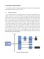
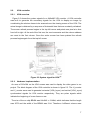
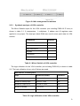
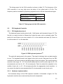
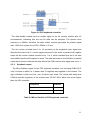
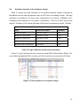
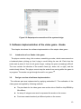
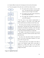
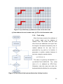
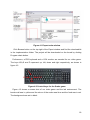
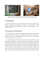
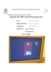
Lund University
Department of Computer Science
EDA 385 the Embedded System Design –
Advanced Course
A Simple Video Game - Snake
Date: 2008-10-18
Students Name: Yuan Mengze ([email protected])
Cai Meng ([email protected])
Project Supervisor: Flavius Gruian & Per Andersson
Abstract
A simple video game ‘snake’ is introduced in this report. The project was based on the
embedded system design which required both hardware and software implementation.
Digilent Nexys2 development board and Xilinx EDK platform were employed in this
project. The project was divided into two parts: the hardware was designed by Yuan
Mengze, which contained a VGA controller and a PS2 keyboard controller, while Cai
Meng programmed the embedded C on the MicroBlaze.
2
CONTENTS
1.
Introduction
5
1.1.Digilent Nexys2 Board
5
1.2.MicroBlaze
5
1.3. EDK
5
2.
Hardware implementation
6
2.1.Hardware overview
6
2.2.VGA controller
7
2.2.1. VGA overview
7
2.2.2. Hardware implementation
7
2.2.3. Synthesis analyzes of VGA controller
9
2.3.PS2 keyboard Controller
2.3.1. PS2 keyboard protocol
10
2.3.2. Hardware implementation
10
2.3.3. Synthesis report
11
2.4.Synthesis analysis of the hardware design
3.
10
Software implementation of the video game - Snake
12
13
3.1.Introduction of our Snake video game
13
3.2.Design overview of software implementation
13
3.3.Detailed descriptions of software design
15
3.3.1. Display
15
3.3.2. Initialization of the game
15
3.3.3. Snake moving function
15
3.3.4. Food eating
16
3.3.5. Delay
17
3.3.6. Game status
17
3.4.Memory size requirement
17
3
4.
Installation and user manual of the video game
17
5.
Contributions
19
6.
Conclusion and future work
19
7.
Reference
20
8.
Acknowledgment
20
4
1. Introduction
This chapter introduces the development board and design tools which were utilized
in this project.
1.1.
Digilent Nexys2 Board
The project was implemented on the Digilent Nexys2 Board which is a powerful digital
system design platform built around a Xilinx Spartan 3E FPGA. The system frequency
of the Nexys2 board is 50 MHz. Figure 1.1 shows the Nexys2 board.
Figure 1.1 Digilent Nexys2 board [2]
1.2.
MicroBlaze
The MicroBlaze is a soft processor core designed for Xilinx FPGAs from Xilinx. As a
soft-core processor, Microblaze is implemented entirely in the general-purpose memory
and logic fabric of Xilinx FPGAs.
1.3.
EDK
Xilinx's EDK (Embedded Development Kit) was employed in this project, which is the
development package for building Microblaze embedded processor systems in Xilinx
FPGAs.
5
2. Hardware implementation
This chapter introduces the hardware implementation in detail. A VGA controller and
a PS2 keyboard controller were built in FPGA.
2.1.
Hardware overview
The on-chip MicroBlaze communicates with the user logics through PLB bus, as
illustrated in figure 2.1. The IP core PLBV4.6 was automatically generated under EDK
platform when a user peripheral was created. The PLBV4.6 generates a simplified PLB
bus for the user logics. The on-chip Block Select RAMs were used to store the pixel
data, which were generated by the MicroBlaze and transferred through PLB bus. The
VGA controller was combined with synchronization counters and address generators.
The counters generated the horizontal and vertical synchronize signals for the VGA
monitor. While the address generator generated the address for reading the pixel data
from the BRAM and sent them to RGB ports of the VGA monitor. The PS2 controller
received the scan code from keyboard in serial and sent it to MicroBlaze through PLB
bus in parallel. XPS_Timer is the IP core provided by Xilinx, which was used to
generate random data for MicroBlaze. More detailed description of XPS_Timer will be
introduced later in the software design.
Figure 2.1 Design overview
6
2.2.
VGA controller
2.2.1.
VGA overview
Figure 2.2 shows the system signals for a 640x480 VGA monitor. A VGA controller
was built to generate the necessary signals for the VGA to display an image by
coordinating the electron beam to be scanned over the viewing screen of the VGA. The
actual image is obtained by a sequence of horizontal lines that are constantly refreshed.
The screen refresh process begins in the top left corner and paints one pixel at a time
from left to right. At the end of the first row, the row increments and the column address
are reset to the first column. Once the entire screen has been painted the refresh
process begins again from the top left corner.
Figure 2.2 System signal for VGA [3]
2.2.2.
Hardware implementation
An area of 512x384 on the VGA screen was used to display the video game in our
project. The block diagram of the VGA controller is shown in figure 2.3. The H_counter
and V_counter were used to generate horizontal (VGA_hsync) and vertical (VGA_vsync)
synchronized signals for VGA monitor respectively. They are pulse signals which
indicate the beginning of a new frame or row.
The size of the on-chip BRAM was 64x48x2 = 6144bit, which indicates that the length
was 3072 and the width of the BRAM was 2 bit. Therefore 4 different colours were
7
available for the VGA. The detailed description of Bram utilization is introduced in
software sections.
Figure 2.3 VGA controller
Reading address for BRAM was provided by the address generator and the read
control signal was given by the control signal component. The address generator was
controlled by Pixel_enable and Clock_divider components. The frequency of the VGA is
25 MHz while the system clock is 50MHz. Therefore a clock divider was applied for
generating 25MHz clock signal to the address generator. Since only an area of 512x384
on the VGA screen were used in this project, the range of the address for BRAM was
from 0 to 512x384 -1, which indicates that the output of the address generator was18 bit
wide. As shown in figure 2.4, the bits from 0 to 8 represent the pixels in a row while the
bits from 9 to 17 represent the vertical lines of the VGA. The length of the BRAM was
64x48 as mentioned previously and the address width for BRAM was 12 bit. Therefore
we extracted appropriate bits from the output of the address generator and combined
them as the address for the BRAM, as shown in figure 2.4. The 3 to 8 bits were
extracted for horizontal lines and 12 to 17 bits were extracted for vertical lines. Then the
data in a memory slot represented 64 pixels on VGA screen instead of 1 pixel as
512x384 is 64 times of 64x48.
The two bits output of the BRAM was the control signal for the colour_gen component
which generated appropriate colours to VGA monitor.
8
Figure 2.4 bits arrangement for address
2.2.3.
Synthesis analyzes of VGA controller
The Micro Statistic report for the VGA controller (not including PLBV4.6 IP core) is
shown in table 2.1. 8 comparators, 1 multiplexer, 3 adders and 43 registers were
applied in our project. The dual port block RAM was used to store pixel data for VGA
monitor.
Components
Utilization
1072x2-bit dual port block RAM
2
4x8-bit ROM
1
Adders/subtractors
3
Registers
43
Comparators
8
Multiplexers
1
Table 2.1 Micro Statistic of VGA controller
The logic utilization for the VGA controller (not including PLBV4.6) is shown in table
2.2. The logic utilization is low, only 66 slices are used.
Select Device: 3s1200efg320-4
Logic
Used and Available
Utilization
Number of slices
66 out of 8672
0%
Number of slice flip flops
42 out of 17344
0%
Number of 4 input LUTs
121 out of 17344
0%
Number of BRAMs
1 out of 24
3%
Number of bonded IOBs
63 out of 250
25%
Table 2.2 Logic Utilization of the VGA controller
9
The timing report for the VGA controller is shown in table 2.3. The frequency of the
VGA controller is not very high since the delay of the critical path is 12.2ns. The
frequency can be increased by pipelining registers and cut off the combinational logics.
Select Device: 3s1200efg320-4
Minimum period
12.201ns
Maximum Frequency
81.961MHz
Table 2.3 Timing report of the VGA controller
2.3.
PS2 keyboard Controller
2.3.1.
PS2 keyboard protocol
The keyboard uses a serial protocol with 11-bit frames, as illustrated in figure 2.5. The
first bit is a start bit which is followed by 8 data bits scan code or released code. The
parity bit is set if there is an even number of 1's in the data bits and reset (0) if there is
an odd number of 1's in the data bits.
Figure 2.5 PS2 keyboard protocol [4]
The parity bit was ignored in the project. The stop bit indicates that one data transfer
is over. The keyboard sends clock signal to the host as well. Data sent from the PS2
controller to the host is read on the falling edge of the clock signal. The clock frequency
must be in the range 10 - 16.7 kHz which means that the clock must be high for 30 - 50
microseconds and low for 30 - 50 microseconds. Data line should be sampled in the
middle of each cell, i.e.15 - 25 microseconds after the appropriate clock transition. In
our project the data line was sampled after 25 microseconds in each clock cycle.
2.3.2.
Hardware implementation
The hardware design of the PS2 keyboard controller is illustrated in figure 2.6. The
keyboard controller was constructed by three sub components.
10
Figure 2.6 PS2 keyboard controller
The data enable module sent an enable signal to the bit counter module after 25
microseconds, indicating that the one bit data can be sampled. The system clock
frequency is 50MHz; therefore the data enable module generated the enable signal
after 1250 clock cycles since 1250 / 50MHz = 25 ms.
The bit counter counted from 0 to 10 according to the keyboard clock signal and
detected the start bit at 0. A store signal was sent to the serial to parallel shift register
when the bit counter module counted from 1 to 8, which indicated that the 8 bit data
were shifted into the shift register in serial. The data were sent to the PLB bus in parallel
when the bit counter detected the stop bit and the PLB read no write signal was set to 1.
2.3.3.
Synthesis report
The Micro Statistic report for the PS2 keyboard controller (not including PLBV4.6 IP
core) is shown in table 2.4. 2 adders and 13 registers were applied in this module. The
logic utilization is also very low, only 43 slices were used. The critical path delay was
6.442ns and the frequency of the module was 155.231 MHz, which was much higher
than the VGA controller.
Components
Utilization
Adders/subtractors
2
Registers
13
Table 2.4 Micro Statistic of PS2 keyboard controller
11
2.4.
Synthesis analysis of the hardware design
Table 2.5 shows the logic utilization of the system hardware design, including the
MicroBlaze and all other peripherals such as XPS timer and debug module. The logic
utilization is increased a lot since more components are involved. 9 BRAMs and 3
multipliers were employed in our project. Furthermore, 1760 out of 8672 slices were
applied. The delay of the critical path was 9.667ns and the frequency was 93.744 MHz.
Select Device: 3s1200efg320-4
Logic
Used and Available
Utilization
Number of slices
1760 out of 8672
20%
Number of slice flip flops
1989 out of 17344
11%
Number of 4 input LUTs
2723 out of 17344
15%
Number of BRAMs
9 out of 28
32%
Number of MULT18X18SIOs
3 out of 28
10%
Table 2.5 Logic utilization of the system hardware
Figure 2.7 and 2.8 shows the bus connection under EDK Xilinx Platform Studio. The
user defined peripherals PS2 controller and VGA controller are connected to PLB bus.
Figure 2.7 Bus interface of the system design
12
Figure 2.8 Output ports connection of the system design
3. Software implementation of the video game - Snake
This chapter introduces the software implementation of the simple video game.
3.1.
Introduction of our Snake video game
The player controls a long, thin creature, resembling a snake, which roams around on
a bordered plane, picking up food, trying to avoid hitting its own tail. Each time the
snake eats a piece of food, its tail grows longer, making the game increasingly difficult.
The user controls the direction of the snake's head (up, down, left, or right), and the
snake's body follows. The player cannot stop the snake from moving while the game is
in progress. The snake can go through the wall in our game. [5]
3.2.
Design overview of software implementation
The software part was implemented by applying embedded C. The realization of the
video game was applied by following methods.
z
The pixel data for the video game were written into a 64x48 on chip BRAM by
MicroBlaze
z
An array of integers was used to represent the snake on the screen
z
Food was created randomly at different points on the screen
13
z
Specify different colours for the background, food, wall and the snake
z
The moving speed of the snake was controlled by a delay function
z
The game will be ended in two way: game
over – the snake hits itself or win the game –
reach the maximum length of the snake
z
The length of the snake will be increased by
one if the snake eats a food
z
The snake was controlled by direction key
on the PS2 keyboard
The flow chart of the software implementation is
shown in figure 3.1. The colour of the border wall,
snake and the food are initialized at Initial Game step.
The snake moves according to the direction keys at
Moving step. The Meet food step detects whether the
snake eat a food after its movement. If yes, then goes
to Node increment & Food generated step. If no, then
goes to key Protected & Delay for moving step.
The length of the snake will increase by one and
generate a new food at Node increment step & Food
generated step.
The Game Over step detect whether the snake hits
itself. If yes, then a new game is started. If no, then
goes to Win the game step.
At Win the game step, if the length of the snake is
equal to the maximum length, then a new game is
started as in Game Over step. If not, the game
continues. The maximum length of the snake in our
design is 100 nodes.
Figure 3.1 System Flow chart
14
3.3.
Detailed descriptions of software design
3.3.1.
Display
The pictures displayed on the VGA screen are realized by setting appropriate pixel
values to the on-chip BRAM. The two bit data in a memory slot represent an 8x8 pixel
area on the VGA screen, named pixel point in this report. Each pixel point on the
screen has its exclusive a and b coordinate and its absolute address in the BRAM is
generated according to equation below
Address = (base address) + a + b x (width of the game)
The base address of the BRAM can be found in xparameter.h file and the term a + b
x (width of the game) is the offset of the base address.
3.3.2.
Initialization of the game
The game is initialled at the Initial game step which includes background initialization,
drawing the border of game area, snake initialization and generating the first food.
First of all, the game background is set to black colour. Then the boarder wall is
drawn as yellow colour, which indicates the area of the video game. The width of the
boarder is 2 pixel points and the area of the video game is 40x30 pixel point.
The snake is initialized by setting the following data: Snake’s head position on the
screen, the moving direction of the snake and the initialized length of the snake. The
positions of the nodes which follow the snake’s head are set according to the address of
the snake’s head and moving direction of the snake.
The first food is initialized by generating a random position on the screen, and food
flag is set to ‘0’, which indicates that a food exists on screen.
3.3.3.
Snake moving function
3 steps are needed for a snake movement, as illustrated in figure 3.2. First of all, the
last node of the snake is set to background colour, as shown in 3.2(b). Each snake
node copies the address from previous node except the first node at second step. The
address of the first snake node is generated according to the moving direction. Then the
first node of the snake is filled with snake colour as shown in 3.2(d)
15
Figure 3.2 (a) Initial step, (b) Remove colour of the last node
(c) New address for each snake node, (d) Fill in the first snake node
3.3.4.
Food eating
Meet food step examine the address of
the snake’s head and the address of
random food. The snake eats the food
when those two addresses are equal, then
the length of the snake increases by one. A
random address for the new food is
generated by my_rand (a, b) function. It
generates a random number between b
and a by using the equation below:
y=x %( b-a) +a
The value x is given by the equation x =
((x+34213)*71411-34267)*59.
The
initial
value of x is obtained by XPS_Timer.
Otherwise, skip this step and enter the
keyboard detection& delay for moving step.
Figure 3.3 Flow chart of the keyboard detection & delay function
16
3.3.5.
Delay
The flow chart for keyboard detection & delay for moving step is shown in figure 3.3.
The moving speed of the snake is set by using a delay function after snake movement.
A counter will count from initial value to 0.
The interrupt based PS2 keyboard controller was not used in this project. Therefore
the keyboard detection is done by keeping reading the registers of the PS2 controller in
the delay function. When a key was pushed and detected, the moving direction will be
changed according to current direction of the snake and the scan code of the pushed
button. Then the program breaks the delay function. Otherwise, the delay function will
not be ended until the counter counts to 0.
3.3.6.
Game status
There are two possible ways to end the video game: game over or win. Game over
step detects whether the snake hits itself, which means that the address of the head is
equal to the address of any other snake node. The game is not over when the snake
hits the well. The snake will go through the well and appear on other side of the game
area. Win the game step detects whether the length of the snake reaches the maximum
value. The Start a new game step initializes the game again if game over or wins the
game happens.
3.4.
Memory size requirement
The memory size for the software is 8 k in total, since the program is small. The BRAM
size occupied for MicroBlaze is 16 KB, which was set in the beginning of the project.
Therefore the memory size is enough for our project.
4. Installation and user manual of the video game
The download.bit file will be generated when the software is complied successfully
and hardware bitstream is generated in EDK Xilinx Platform Studio. In order to
download the project on the Digilent development board, the Digilent Adept Suite needs
to be downloaded from the Digilent home page: www.digilentinc.com. After installing the
Digilent Adept Suite, start the Export as shown in figure 4.1.
17
Figure 4.1 Export main window
Click Browse button on the top right of the Export window and find the download.bit
in the implementation folder. The project will be downloaded on the board by clicking
Program chain button.
Furthermore, a PS2 keyboard and a VGA monitor are needed for our video game.
The keys W,A,S and D represent up, left, down and right respectively, as shown in
figure 4.2.
Figure 4.2 Control keys for the Snake game
Figure 4.3 shows a screen shot of our video game and the lab environment. The
border wall was in yellow and the colour of the snake was blue and the food was in red.
The background was set to black.
18
Figure 4.3 Screen shot and lab environment of the video game Snake
5. Contributions
The project was divided into two parts and we were two people in a group. Yuan
Mengze accomplished the hardware part, including a VGA controller and a PS2
controller. Cai Meng realized the video game Snake by applying embedded C on the
hardware platform.
6. Conclusion and future work
We have completed our knowledge of embedded system design after we finished the
project and obtained more experience of hardware/software co-design. Since it was the
first time that we built an embedded system on our own, a lot of problems were
encountered during our work on the project.
For the hardware part, we took a long time to familiar with the protocol of all the
peripherals and the PLB bus specification. Then the VGA controller was accomplished
in two weeks after reading the reference design provided by the Digilent home page and
the PS2 controller was built in an afternoon. One of the most important problems of our
hardware design was the frequency difference. The system frequency is 50MHz while
the VGA monitor is 25 MHz, therefore a clock divider is needed for our design. We
didn’t notice that in the very beginning and it took a long time to fix the problem. Another
problem was the complexity of the PLB bus interface. We took a long time to familiar
19
with the control signals provided by PLB bus. But now we have more experience of
interfacing the PLB bus with other peripherals.
For the software part, we test our program by applying Visual C at the beginning.
Then we encountered some problems when we implemented our program on the onchip MicroBlaze. Although the basic syntax of the general C and embedded C are
almost the same, the difference between them can not be ignored. The library provided
by MicroBlaze is much less than in PC, therefore we have to write our own functions
instead. For instance, we wrote a function to generate random data which has the same
functionality of the rand () in general C programming. Another difference that needs to
be taken into account is the address of the memory. In general C, the addresses for the
VGA screen are generated by functions, while for embedded system design, we have to
generate the addresses for the BRAM by adding the offset to the base address of the
BRAM.
The project can be extended and optimized if we have enough time. For instance, a
microphone can be used to generate the background music of our video game. 7
segment led can be employed to display the scores of the game and setting bonus food
for the snake can be added as well.
7. Reference
[1] http://www.cs.lth.se/EDA385/
[2] Digilent Nexy2 Board Reference Manual
[3] Digilent VGA Component Reference Design
[4] http://www.computer-engineering.org/ps2protocol/
[5] http://www.wikipedia.org/
8. Acknowledgment
Finally thanks for the help given by the project supervisors Flavius Gruian, Per
Andersson and thanks for the help from our great classmates: Li Jia from Teris group
and Wee Guan Lim & Lay Hong Ang from Zuma group.
20