1
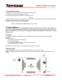
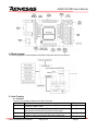
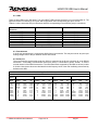
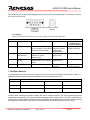
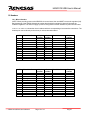
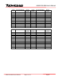
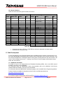
Applications Engineering
3DK2218U USB Kit
User’s Manual
Rev. 1.0
August 2007
H8S/2218 USB User’s Manual
Preface
Cautions
1.
This document may be, wholly or partially, subject to change without notice.
2.
All rights reserved. No one is permitted to reproduce or duplicate, in any form, a part or this entire
document without Renesas Technology Europe Limited’s written permission.
Trademarks
General All brand or product names used in this manual are trademarks or registered trademarks of their
respective companies or organisations.
Document Information
Date: 08/01/2007
Copyright © Renesas Technology America Ltd. 2007. All rights reserved.
Copyright © Renesas Technology Europe Ltd. 2007. All rights reserved.
Website:http://www.america.renesas.com/
3DK2218 USB Kit User’s Manual
Page 2 of 12
Aug-07
H8S/2218 USB User’s Manual
Table of Contents
1. Power Requirements ................................................................................4
2. Power-up Behaviour .................................................................................4
3. Purpose .....................................................................................................4
4. Board Layout.............................................................................................4
5. Block Diagram...........................................................................................5
6. User Circuitry ............................................................................................5
7. Oscillator Sources ....................................................................................7
8. Modes ........................................................................................................8
9. Programming Methods and 2218UF Kernels..........................................8
10 Headers...................................................................................................10
11 Code Development ................................................................................12
3DK2218 USB Kit User’s Manual
Page 3 of 12
Aug-07
H8S/2218 USB User’s Manual
1. Power Requirements
All 3DK boards are centre positive with a 2.5mm barrel power jack.
The diode, D1 provides reverse polarity protection.
A 9V, centre positive supply is suitable for use with this board.
Warning
Check the silkscreen around the power jack (J9) for the minimum and maximum voltage input levels for this 3DK.
The 3DK is neither under nor over voltage protected.
Always use a centre positive supply for this board.
DO NOT USE AN E6000 POWER SUPPLY with this 3DK
2. Power-up Behaviour
The 3DK2218 USB kit has code pre-programmed into the Renesas microcontroller which allows it to
enumerate as a Mass Storage Class USB device. On powering up the board, the red user LEDs will start to
flash in a sequential manner and upon connecting the USB cable the H8S/2218 enumerates as a mass
storage device.
3. Purpose
This 3DK2218 USB kit is an evaluation tool for the H8S/2218 Renesas microcontroller and on-chip USB
peripheral.
Features include:
a. Renesas Microcontroller Programming
b. User Code Debugging
c. User Circuitry such as Switches, LEDs and potentiometer(s)
d. User or Base Board Connectivity
The 3DK board contains all the circuitry required for microcontroller operation.
4. Board Layout
The following diagram shows the component layout top layer component of the board.
Note: The diagram below is for illustrative purposes and does not accurately reflect the 3DK detailed in this
manual.
3DK2218 USB Kit User’s Manual
Page 4 of 12
Aug-07
H8S/2218 USB User’s Manual
5. Block Diagram
The following diagram is representative of the 3DK components and their connectivity.
6. User Circuitry
6.1. Switches
There are four switches located on the 3DK. These are:
Switch
Function
SW1/Boot
This switch is used in conjunction with the RES switch to place
the device in BOOT mode.
SW2
This switch is connected via a 0R link to an IRQ line capable of
waking up the microcontroller device from sleep mode.
SW3
This switch is connected via a 0R link to another IRQ line capable
of waking up the microcontroller device from sleep mode.
RES
This switch when pressed resets the 3DK microcontroller.
3DK2218 USB Kit User’s Manual
Page 5 of 12
Microcontroller
IRQ2 (Pin 97)
IRQ4 (Pin 24)
IRQ7 (Pin 25)
RESn
Aug-07
H8S/2218 USB User’s Manual
6.2. LEDs
There are nine LEDs on the 3DK board. The green BOOT LED indicates the device is in boot mode when lit. The
eight red LEDs are connected to an IO port and will light when their corresponding port pin is set low.
Table 6-1 below, shows the LED pin references and their corresponding microcontroller port pin connections.
LED Reference (As shown on
silkscreen
CLED1
CLED2
CLED3
CLED4
CLED5
CLED6
CLED7
CLED8
Microcontroller Port Pin function
Microcontroller Pin Number
PE0
PE1
PE2
PE3
PE4
PE5
PE6
PE7
Table 6-1: LED Port
Pin 64
Pin 65
Pin 66
Pin 67
Pin 68
Pin 69
Pin 70
Pin 71
6.3. Potentiometer
A single turn potentiometer is connected to AN0 of the microcontroller. This may be used to vary the input
analog voltage value to this pin between AVCC and Ground.
6.4. Serial port
The microcontroller programming serial port (SCI2) is connected to the D.type connector J8 via an RS232
transceiver. A secondary microcontroller serial port (SCI2) is connected to generic header, J6 via the
second channel of the RS232 transceiver. The serial baud rates supported by this 3DK are shown in table
6-2 below. Note: these values are calculated from the frequency value of the main oscillating source fitted by
default on this 3DK.
Baud Rate Settings for Serial Communication Rates
Values are calculated for 24MHz clock
SMR
Setting
Comm.
Baud
110
300
1200
2400
4800
9600
19200
38400
57600
115200
0
BRR
setting
invalid
invalid
invalid
invalid
155
77
38
19
12
6
Actual
Rate
invalid
invalid
invalid
invalid
4808
9615
19231
37500
57692
107143
1
ERR
(%)
invalid
invalid
invalid
invalid
0.16
0.16
0.16
-2.34
0.16
-6.99
BRR
setting
invalid
invalid
155
77
38
19
9
4
2
1
Actual
Rate
invalid
invalid
1202
2404
4808
9375
18750
37500
62500
93750
2
ERR
(%)
invalid
invalid
0.16
0.16
0.16
-2.34
-2.34
-2.34
8.51
-18.62
BRR
setting
Invalid
155
38
19
9
4
1
0
invalid
invalid
Actual
Rate
invalid
300
1202
2344
4688
9375
23438
46875
invalid
invalid
3
ERR
(%)
Invalid
0.16
0.16
-2.34
-2.34
-2.34
22.07
22.07
invalid
invalid
BRR
setting
106
38
9
4
1
0
Invalid
Invalid
Invalid
invalid
Table 6-2: BRR Settings
3DK2218 USB Kit User’s Manual
Page 6 of 12
Aug-07
Actual
Rate
110
300
1172
2344
5859
11719
Invalid
Invalid
Invalid
invalid
ERR
(%)
-0.44
0.16
-2.34
-2.34
22.07
22.07
Invalid
Invalid
Invalid
invalid
H8S/2218 USB User’s Manual
This serial port may be used as a debugging communication port or as a normal serial communication port when
the device is in user mode.
6.5. Jumpers
Table 6-3 below describes the function of the 2-Pin jumpers contained on this 3DK board.
Reference
2-pin jumper settings
Fitted
Jumper Function
J10
RX Disable
PRXD from the RS232 device
to U1 is enabled. This enables
serial port communication.
J11
UVCC power
Measurement
J14
FWE (Flash Write
Enable)
J15
EMLE
Bypasses R11, a 1206 0R
resistor, for current
measurement
Disables all flash
programming, even in BOOT
mode
Disables the E10A interface.
Alternative
Disabled. This
allows the FDM to
program the
microcontroller
R11 must be fitted to
power UVCC
Enables Flash
programming
Enables the E10A
interface
Table 6-3: 2-pin jumpers
Footprint for
Jumper only/
Jumper pins fitted
Jumper pins fitted
(2-way connector)
Footprint only
Footprint only
Jumper pins fitted
(2-way connector)
7. Oscillator Sources
A crystal is fitted on the 3DK and used to supply the main clock input to the Renesas microcontroller. Table 7-1
details the oscillators that are fitted and alternative footprints provided on this 3DK:
Component
Resonator
Crystal
Subclock
Footprint Only (4.1mm x 4.7mm)
Details
24MHz (recommended)
Serial Baud Rate: 115200
Fitted (7.5mm x 5.0mm)
24MHz
Serial Baud Rate: 115200
Yes
32.76KHz
N\A
Table 7-1: Oscillators / Resonators
Warning: When replacing the default oscillator with that of another frequency, the FDT programming kernels
supplied will need rebuilding. The supplied HMON debugging monitor will not function. The user is responsible for
code written to support operating speeds other than the default. See the HMON user manual for details of making
the appropriate modifications in the code to accommodate different operating frequencies of the device
3DK2218 USB Kit User’s Manual
Page 7 of 12
Aug-07
H8S/2218 USB User’s Manual
8. Modes
The 3DK supports User mode and Boot mode. User mode may be used to run, debug and program user code,
while Boot mode may only be used to program the Renesas microcontroller with code. To enter boot mode, the
mode pins are held in their boot states while reset is pressed and released. The BOOT LED will be illuminated to
indicate that the microcontroller is in boot mode.
8.1. Boot Mode
The boot mode settings for this 3DK are shown in Table 8-1 below:
MD2
1
0
MD1
1
1
MD0
LSI State after Reset End
0
User Mode
X (MD0 pin pulled low on 3DK)
Boot Mode
Table 8-1: Mode pin settings
8.2. User Mode
For the device to enter User Mode, reset must be held active while the microcontroller mode pins are held in
states specified for User Mode operation. 100K pull up and pull down resistors are used to set the pin states
during reset. The H8S/2218U supports single advanced mode, advanced mode with ROM enabled and
advanced mode with ROM disabled.
9. Programming Methods and 2218UF Kernels
There are two methods of programming. These are boot mode programming and user mode programming. The
device must be in the boot mode for boot mode programming and in a user mode (with ROM enabled) for user
mode programming.
9.1. Boot Mode
Boot mode may be used to program a blank device. Once in boot mode, the boot loader program stored in
the microcontroller executes and attempts a connection with a host (for example, a PC). The host, on
establishing a connection with the microcontroller, may then transmit program data to the microcontroller via
the appropriate programming port. All data in the flash memory will be erased before programming of the
device will begin. When in boot mode, the H8S/2218UF device attempts communication with a host via the
USB port. The user cannot change this boot programming port to another port.
9.2. User Mode
User mode programming is used to program a microcontroller device when the device is in user mode (with
ROM enabled). This programming method also allows the user to program the device without first erasing all
of its flash memory. To initiate user mode programming, the device must already contain user mode
programming code in its Flash memory. In user mode, the user mode programming code stored in the
device executes and attempts a connection with a host. The host may then erase some of the device’s
memory, perform a blank check, upload data from the device and program the device. The H8S/2218UF
user mode kernels are written to establish a connection with a host via the serial port.
9.3. 2218F Kernels and Programming ports
The H8S/2218UF kernels are designed to program the device via the USB port when in boot mode, and the
serial port when in user programming mode.
3DK2218 USB Kit User’s Manual
Page 8 of 12
Aug-07
H8S/2218 USB User’s Manual
Table 9-1 below shows the programming port for this Renesas Microcontroller and its associated pins
Programming port table – Programming port pins and their 3DK signal names
Boot Mode
USB
D+, pin 32
D-, pin33
programming via the
3DK Signal Name
USD_Plus
USD_Minus
USB port
User Mode
SCI2
TXD2, pin 100
RXD2, pin 99
SCK2, pin 98
programming via the
3DK Signal Name
PTXD
PRXD
PSCK
serial port
Table 9-1: Serial Port Boot Channel
9.4. Boot Programming Procedure
The microcontroller must enter boot mode for boot programming. The programming port (USB) must be
connected to a host for program download. To execute the boot transition, and allow programs to download
to the microcontroller, the user must perform the following procedure:
1.
2.
3.
4.
Connect a USB cable between the host PC and the 3DK board
Depress the RESET switch and keep this held down
Depress the BOOT switch once, and release
Release the RESET switch
9.5. FDM Header
The Renesas FDM (Flash Debug Module) is a USB based programming tool for control and programming of
Renesas microcontrollers, available separately from Renesas.
The FDM is not supported by this 3DK as this device uses the USB port for boot mode programming.
9.6. E10A Header
The Renesas E10A Debugger is a tool for debugging Renesas microcontrollers, available separately from
Renesas. The device may be debugged and programmed using the E10A. The E10A utilises H-UDI pins on
the H8S/2218U device.
To utilise this header the user must make the following changes to the board configuration.
1. Jumper link J15 must be removed
9.7. Off-Board Programming
All 3DKs are capable of programming an alternative microcontroller on a secondary board. The user is
responsible for providing this second board containing the alternative microcontroller, its supporting circuitry
and an FDM or FoUSB header for the microcontroller.
To program the alternative microcontroller, the user should perform the following steps
•
•
Connect a cable between the 3DK programming header and that located on the secondary board.
Slide switch MCU_SEL to the off-board programming position (OFF). This holds the microcontroller
on the 3DK in reset, preventing it from being programmed.
3DK2218 USB Kit User’s Manual
Page 9 of 12
Aug-07
H8S/2218 USB User’s Manual
10 Headers
10.1. Micon Headers
NOTE: When providing power to the 3DK2218 via a user board, the user MUST remove the regulator (U4).
Back-powering of the 3DK2218 board via another board with the regulator in place will damage the
3DK2218 regulator. This does not apply if power is being taken from the 3DK2218 to power a user board.
Table 10-1 to Table 10-4 shows the micon headers and their corresponding microcontroller connections. The
header pins connect directly to the micon pin unless otherwise stated.
J1 Pin
Circuit Net Name
U1 pin
J1 pin
number
number
1
2
3
4
5
6
7
8
9
10
11
12
13
14
15
16
17
18
19
20
21
22
23
24
Table 10-1: J1
Circuit Net Name
U1 pin
number
2
4
6
8
10
12
14
16
18
20
22
24
Circuit Net Name
U1 pin
J2 pin
number
number
25
2
27
4
29
6
31
8
33
10
35
12
37
14
39
16
41
18
43
20
45
22
47
24
49
26
Table 10-2: J2
Circuit Net Name
U1 pin
number
26
28
30
32
34
36
38
40
42
44
46
48
50
1
3
5
7
9
11
13
15
17
19
21
23
J2 Pin
1
3
5
7
9
11
13
15
17
19
21
23
25
Board_Vcc
NC
CON_Vref
3DK2218 USB Kit User’s Manual
Page 10 of 12
NC
Ground
Ground
Board_Vcc
Aug-07
H8S/2218 USB User’s Manual
J3 Pin
1
3
5
7
9
11
13
15
17
19
21
23
J4 Pin
Circuit Net Name
CON_OSC2
Ground
CON_Extal
Circuit Net Name
1
3
5
7
9
11
13
15
17
19
21
23
25
3DK2218 USB Kit User’s Manual
U1 pin
J3 pin
number
number
51
2
53
4
55
6
57
8
59
10
61
12
63
14
65
16
67
18
69
20
71
22
73
24
Table 10-3: J3
U1 pin
J4 pin
number
number
75
2
77
4
79
6
81
8
83
10
85
12
87
14
89
16
91
18
93
20
95
22
97
24
99
26
Table 10-4: J4
Page 11 of 12
Circuit Net Name
CON_OSC1
CON-Xtal
Board_Vcc
Circuit Net Name
Board Vcc
Ground
U1 pin
number
52
54
56
58
60
62
64
66
68
70
72
74
U1 pin
number
76
78
80
82
84
86
88
90
92
94
96
98
100
Aug-07
H8S/2218 USB User’s Manual
10.2. Generic Headers
Table 10-5 below shows the generic header connections
Pin
number
1
19 way generic header
Generic
3DK signal
header name
name
Supply
Supply
2
Xin
3
4
5
6
7
8
9
10
11
12
13
14
15
16
17
18
19
Vcc
Vss
Vcc
Vss
AVcc
AVss
Vref
AN0
AN1
AN2
AN3
AN14
AN15
not connected
not connected
not connected
not connected
•
•
20 way generic header
Generic header
3DK signal
name
name
Spare SCI Tx pin
IOPORT_TXD
RS232 levels
CON_Xtal
61*
2
Spare SCI Tx pin
IOPORT_RXD
RS232 levels
Vcc1
N/A
3
TIOCA1
IOPORT_T1
Ground
N/A
4
TIOCB1
IOPORT_T2
Vcc2
N/A
5
TIOCA2
IOPORT_T3
Ground
N/A
6
TIOCB2
IOPORT_T4
NC
N/A
7
IOPORT_U
NC
Ground
N/A
8
IOPORT_V
NC
CON_Vref
41*
9
IOPORT_W
NC
Pin 45 (AN0) 45
10
PE0
IOPORT_0
Pin 44 (AN1) 44
11
PE1
IOPORT_1
Pin 43 (AN2) 43
12
PE2
IOPORT_2
Pin 42 (AN3) 42
13
PE3
IOPORT_3
NC
N/A
14
PE4
IOPORT_4
NC
N/A
15
PE5
IOPORT_5
NC
N/A
16
PE6
IOPORT_6
NC
N/A
17
PE7
IOPORT_7
NC
N/A
18
/Reset
RESn
NC
N/A
19
/NMI
IOPORT_INT
20
Vss
Ground
Table 10-5: Generic Headers
Micon
pin
N/A
Pin
number
1
Micon
pin
22
23
6
7
8
9
N/A
N/A
N/A
64
65
66
67
68
69
70
71
58
81*
N/A
Connected via either a 0R link or a DNF 0R link, refer to the schematic for further details.
Connected via a transceiver chip
11 Code Development
For all code debugging using Renesas software tools, the 3DK2218 board must be connected to a PC via
the E10A-USB debugger (not supplied with the USB kit). After installing the tools (Compiler and HEW), copy
the included workspaces to C:\Workspace before running them; opening them from any other location will
cause a “This workspace has moved…” warning. If you wish to run the workspace from another location
select “OK” and continue.
11.1. Additional Information
For details on how to use High-performance Embedded Workshop (HEW), refer to the HEW manual
available on the CD or from the website.
For information about the H8S/2218UF series microcontrollers refer to the H8S/2212, 2218 Series
Hardware Manual available on the CD or from the website.
For information about the H8S/2218UF assembly language, refer to the H8S Series Programming Manual
Further information available for this product can be found on the Renesas web site at:
http://www.america.renesas.com/
For technical support/information send an email to [email protected]
3DK2218 USB Kit User’s Manual
Page 12 of 12
Aug-07