1
User Manual
RM3000 & RM2000
Reference Magnetic Sensor Suite
Table of Contents
1
2
3
4
5
6
COPYRIGHT & WARRANTY INFORMATION ............................................................ 4
INTRODUCTION .......................................................................................................... 5
SPECIFICATIONS ....................................................................................................... 6
3.1
RM SENSOR SUITE CHARACTERISTICS .................................................... 6
3.2
SEN-XY AND SEN-Z CHARACTERISTICS.................................................... 7
3.3
3D MAGIC CHARACTERISTICS .................................................................... 8
3.4
TYPICAL SENSOR SUITE OPERATING PERFORMANCE .......................... 9
3.5
DIMENSIONS AND PACKAGING ................................................................. 13
3.5.1 Sen-XY Dimensions & Packaging .................................................... 13
3.5.2 Sen-Z Dimensions & Packaging ....................................................... 14
3.5.1 Sen-Z Shield Dimensions & Packaging ............................................ 16
3.5.2 3D MagIC Dimensions and Packaging ............................................. 17
3.6
SOLDERING ................................................................................................. 19
RM SENSOR SUITE OVERVIEW & SET-UP ............................................................ 21
4.1
OVERVIEW ................................................................................................... 21
4.2
LAYOUT ........................................................................................................ 23
4.2.1 Sensor Orientation ............................................................................ 23
4.2.2 Local Magnetic Field Considerations ............................................... 23
4.2.3 Other Layout Considerations ............................................................ 24
4.3
3D MAGIC PIN-OUT ..................................................................................... 24
4.4
SPI TIMING REQUIREMENTS ..................................................................... 28
4.5
IDLE MODE ................................................................................................... 29
3D MAGIC OPERATION – STANDARD MODE ....................................................... 30
5.1
CYCLE COUNT REGISTERS ....................................................................... 30
5.2
SINGLE-AXIS MEASUREMENT (SAM) OPERATION ................................. 32
5.2.1 SAM SPI Activity Sequence ............................................................. 32
5.2.2 SAM Command Byte ........................................................................ 33
5.2.3 Making a Single-Axis Measurement ................................................. 33
5.3
MULTI-AXIS MEASUREMENT (MAM) OPERATION ................................... 34
5.3.1 MAM SPI Activity Sequence ............................................................. 34
5.3.2 MAM Command Byte ....................................................................... 34
5.3.3 MAM Axes Select Byte ..................................................................... 35
5.3.4 Making a Multi-Axis Measurement ................................................... 35
3D MAGIC OPERATION – LEGACY MODE............................................................. 37
6.1
LEGACY OPERATION .................................................................................. 37
6.1.1 Legacy Operation SPI Activity Sequence......................................... 38
6.1.2 Legacy Command Byte .................................................................... 38
6.1.3 Making a Legacy Measurement ....................................................... 39
6.2
ENHANCED LEGACY OPERATION ............................................................ 40
6.2.1 Clock Divide Command Byte ............................................................ 41
6.2.2 Clock Divide Register ....................................................................... 41
6.2.3 Command Sequence for Setting Clock Divide Value ....................... 42
6.2.4 Changes to the Period Select Value ................................................ 42
List of Figures
Figure 3-1: Sample Rate vs. Resolution – Standard Mode ...................................................... 9
Figure 3-2: Gain vs. Cycle Counts – Standard & Legacy Modes ........................................... 10
Figure 3-3: Single-Axis Sample Rate vs. Cycle Counts – Standard & Legacy Modes .......... 10
Figure 3-4: Gain vs. Cycle Counts – Standard Mode ............................................................. 11
Figure 3-5: Single-Axis Sample Rate vs. Cycle Counts – Standard Mode ............................ 11
Figure 3-6: Current Consumption vs. Cycle Counts – Standard Mode .................................. 12
Figure 3-7: Sen-XY Sensor Dimensions ................................................................................ 13
Figure 3-8: Sen-XY Solder Pad Layout .................................................................................. 13
Figure 3-9: Sen-XY Tape and Reel Dimensions .................................................................... 14
Figure 3-10: Sen-Z Sensor Dimensions ................................................................................. 14
Figure 3-11: Sen-Z Solder Pad Layout ................................................................................... 15
Figure 3-12: Sen-Z Tape and Reel Dimensions ..................................................................... 15
Figure 3-13: Sen-Z Shield Sensor Dimensions ...................................................................... 16
Figure 3-14: Sen-Z Shield Solder Pad Layout ........................................................................ 16
Figure 3-15: Sen-Z Shield Tape and Reel Dimensions .......................................................... 17
Figure 3-16: 3D MagIC MLF Mechanical Drawing ................................................................. 17
Figure 3-17: 3D MagIC MLF Tape Dimensions ...................................................................... 18
Figure 3-18: 3D MagIC Die Pad Layout ................................................................................. 18
Figure 3-19: Example Wire Bonding Layout for Legacy 11096 ASIC Applications ................ 19
Figure 3-20: Recommended Solder Reflow Profile ................................................................ 20
Figure 4-1: RM3000 reference schematic – Standard Mode ................................................. 21
Figure 4-2: LR Oscillator Circuit Biasing Diagram .................................................................. 22
Figure 4-3: RM3000 North-East-Down (NED) Sensor Layout ............................................... 23
Figure 4-4: SPI Timing Diagram ............................................................................................. 28
Figure 5-1: SPI Activity Sequence Diagram for SAM Operation ............................................ 32
Figure 5-2: SPI Activity Sequence Diagram for MAM Operation ........................................... 34
Figure 6-1: SPI Activity Sequence Diagram for Legacy Operation ........................................ 38
List of Tables
Table 3-1:
Table 3-2:
Table 3-3:
Table 3-4:
Table 3-5:
Table 3-6:
Table 4-1:
Table 4-2:
Table 5-1:
Table 5-2:
Table 5-3:
Table 6-1:
Table 6-2:
Table 6-3:
Table 6-4:
RM Sensor Suite Performance ............................................................................... 6
Sen-XY and Sen-Z Absolute Maximum Ratings ..................................................... 7
Sen-XY and Sen-Z Characteristics ......................................................................... 7
3D MagIC Absolute Maximum Ratings ................................................................... 8
3D MagIC Recommended Operating Conditions .................................................... 8
Recommended Solder Processing Parameters .................................................... 20
3D MagIC Pin Assignments .................................................................................. 25
SPI Timing Specifications ..................................................................................... 29
Cycle Count Register Commands ......................................................................... 31
SAM Axis Select Bits ............................................................................................. 33
MAM Axes Select Bits ........................................................................................... 35
Legacy Period Select Bits ..................................................................................... 39
Legacy Axis Select Bits ......................................................................................... 39
Clock Divide Bits ................................................................................................... 41
Enhanced Legacy Mode with CD = 1 .................................................................... 42
RM3000 & RM2000 Sensor Suite User Manual – April 2011
Page 3 of 42
1 Copyright & Warranty Information
© Copyright PNI Sensor Corporation 2010
All Rights Reserved. Reproduction, adaptation, or translation without prior written permission is prohibited, except as allowed under copyright laws.
Revised April 2011: for the most recent version visit our website at www.pnicorp.com
PNI Sensor Corporation
133 Aviation Blvd, Suite 101
Santa Rosa, CA 95403, USA
Tel: (707) 566-2260
Fax: (707) 566-2261
Warranty and Limitation of Liability. PNI Sensor Corporation ("PNI") manufactures its Products from parts and components that are new or
equivalent to new in performance. PNI warrants that each Product to be delivered hereunder, if properly used, will, for ninety (90) days following the
date of shipment unless a different warranty time period for such Product is specified: (i) in PNI’s Price List in effect at time of order acceptance; or (ii)
on PNI’s web site (www.pnicorp.com) at time of order acceptance, be free from defects in material and workmanship and will operate in accordance
with PNI’s published specifications and documentation for the Product in effect at time of order. PNI will make no changes to the specifications or
manufacturing processes that affect form, fit, or function of the Product without written notice to the Customer, however, PNI may at any time, without
such notice, make minor changes to specifications or manufacturing processes that do not affect the form, fit, or function of the Product. This warranty
will be void if the Products’ serial number, or other identification marks have been defaced, damaged, or removed. This warranty does not cover wear
and tear due to normal use, or damage to the Product as the result of improper usage, neglect of care, alteration, accident, or unauthorized repair.
THE ABOVE WARRANTY IS IN LIEU OF ANY OTHER WARRANTY, WHETHER EXPRESS, IMPLIED, OR STATUTORY, INCLUDING, BUT NOT
LIMITED TO, ANY WARRANTY OF MERCHANTABILITY, FITNESS FOR ANY PARTICULAR PURPOSE, OR ANY WARRANTY OTHERWISE
ARISING OUT OF ANY PROPOSAL, SPECIFICATION, OR SAMPLE. PNI NEITHER ASSUMES NOR AUTHORIZES ANY PERSON TO ASSUME
FOR IT ANY OTHER LIABILITY.
If any Product furnished hereunder fails to conform to the above warranty, Customer’s sole and exclusive remedy and PNI’s sole and exclusive liability
will be, at PNI’s option, to repair, replace, or credit Customer’s account with an amount equal to the price paid for any such Product which fails during
the applicable warranty period provided that (i) Customer promptly notifies PNI in writing that such Product is defective and furnishes an explanation of
the deficiency; (ii) such Product is returned to PNI’s service facility at Customer’s risk and expense; and (iii) PNI is satisfied that claimed deficiencies
exist and were not caused by accident, misuse, neglect, alteration, repair, improper installation, or improper testing. If a Product is defective,
transportation charges for the return of the Product to Customer within the United States and Canada will be paid by PNI. For all other locations, the
warranty excludes all costs of shipping, customs clearance, and other related charges. PNI will have a reasonable time to make repairs or to replace
the Product or to credit Customer’s account. PNI warrants any such repaired or replacement Product to be free from defects in material and
workmanship on the same terms as the Product originally purchased.
Except for the breach of warranty remedies set forth herein, or for personal injury, PNI shall have no liability for any indirect or speculative damages
(including, but not limited to, consequential, incidental, punitive and special damages) relating to the use of or inability to use this Product, whether
arising out of contract, negligence, tort, or under any warranty theory, or for infringement of any other party’s intellectual property rights, irrespective of
whether PNI had advance notice of the possibility of any such damages, including, but not limited to, loss of use, revenue or profit. In no event shall
PNI’s total liability for all claims regarding a Product exceed the price paid for the Product. PNI neither assumes nor authorizes any person to assume
for it any other liabilities.
Some states and provinces do not allow limitations on how long an implied warranty lasts or the exclusion or limitation of incidental or consequential
damages, so the above limitations or exclusions may not apply to you. This warranty gives you specific legal rights and you may have other rights that
vary by state or province.
PNI Sensor Corporation
RM3000 & RM2000 Sensor Suite User Manual – April 2011
Doc #1015673 r06
Page 4 of 42
2 Introduction
Thank you for purchasing PNI Sensor Corporation’s RM2000 or RM3000 Reference Magnetic
Sensor Suite (pn 90042 and pn 90043, respectively). The RM2000 is comprised of two Sen-XY
Reference Magnetic Sensors (pn 12683) and a 3D MagIC ASIC MLF controller (pn 12927), and
this forms the basis for a 2-axis (horizontal) digital compass. The RM3000 is the same as the
RM2000 but adds a Sen-Z Reference Magnetic Sensor (pn 12779), such that compassing
measurements are not constricted to the horizontal plane.
When implementing an RM3000 or RM2000 Reference Magnetic Sensor Suite, each Reference
Magnetic Sensor serves as the inductive element in a simple LR relaxation oscillation circuit,
with the sensor’s effective inductance proportional to the magnetic field parallel to the sensor
axis. The LR circuit is driven by the 3D MagIC ASIC. Since the LR circuit’s oscillation
frequency varies with the strength of the magnetic field parallel to the sensor, the 3D MagIC’s
internal clock is used to measure the circuit’s oscillation frequency (cycle counts) and hence the
magnetic field. The 3D MagIC also contains an interface circuitry to communicate with a host
microprocessor on an SPI bus. The 3D MagIC can control and measure up to three PNI
Reference Magnetic Sensors, with each sensor individually selected for measurement and
individually configured for measurement gain (resolution).
Since the Reference Magnetic Sensor Suite works in the frequency domain, resolution and noise
are established cleanly by the number of cycle counts. In comparison, fluxgate and MR
technologies require expensive and complex signal processing to obtain similar resolution and
noise, and in many respects the Reference Magnetic Sensor Suite’s performance simply cannot
be matched. Also, the output from the 3D MagIC is inherently digital and can be fed directly
into a microprocessor, eliminating the need for signal conditioning or an analog/digital interface
between the sensor and a microprocessor. The simplicity of the Reference Magnetic Sensor
Suite combined with the lack of signal conditioning makes it easier and less expensive to
implement than alternative fluxgate or magneto-resistive (MR) technologies.
For more information on PNI’s magneto-inductive sensor technology, see PNI’s whitepaper
“Magneto-Inductive Technology Overview” at http://www.pnicorp.com/technology/papers.
Note: PNI’s Sen-Z Shield is available as an option to provide mechanical protection to the Sen-Z sensor
since the solder joint that attaches the Sen-Z to the user’s PCB may break if the Sen-Z is impacted. The
Sen-Z shield generally should not be required in a well-controlled, high-volume production environment,
but may be advisable for product development and testing or in less-controlled production environments.
RM3000 & RM2000 Sensor Suite User Manual – April 2011
Page 5 of 42
3 Specifications
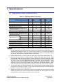
3.1 RM Sensor Suite Characteristics
Table 3-1: RM Sensor Suite Performance1
Parameter
Min
Field measurement range
2
Gain @ 200 Cycle Counts
Typical
-1100
3
Max
Units
+1100
T
45
counts/ T
35
nT
Maximum Sample Rate, Single Axis @
4
200 Cycle Counts
450
Hz
Linearity - best fit over 200 T
0.6
Average Current per Axis @ 35 Hz and
5
@ 200 Cycle Counts
0.3
Noise @ 200 Cycle Counts
Bias Resistance (RB)
3
2.6 V to 3.3 V
68
1.6 V to 2.6V
33 + (V-1.6)*35
1.0
% of 200 T
mA
External Timing Resistor for Clock (REXT)
33
k
Circuit Oscillation Frequency
185
kHz
High Speed Clock Frequency
45
MHz
Operating Temperature
-40
+85
C
Footnotes:
1. Specifications subject to change. Unless otherwise noted, performance characteristics assume
the user implements the recommended bias resistors and external timing resistor for the highspeed clock (as indicated in Figure 4-1 ), the DC supply voltage is 3.3 V, and the 3D MagIC is
operated in Standard Mode. Other bias resistors, external timing resistors and operating voltages
may be used, but performance may differ from the values listed.
2. Field measurement range is defined as the monotonic region of the output characteristic curve.
3. Gain and noise are related to useable resolution. Below ~200 cycle counts the gain setting
dominates the usable resolution (resolution = 1/gain) while above ~200 cycle counts the system
noise dominates. The user establishes the gain value by setting the Cycle Count Register value.
See Figure 3-4 for the typical relationship between cycle counts, gain, and resolution. Above
~200 cycle counts noise is relatively constant and there are diminishing returns in usable
resolution as the cycle count value increases. Also, performance will vary from sensor to sensor:
~50% of the sensors will have performance greater than “Typical” and ~50% less than “Typical”.
4. The maximum sample rate and gain/resolution are inversely related, so higher sample rates can
be obtained by reducing the number of cycle counts, but this also results in reduced gain and
resolution. Also see Figure 3-4 and Figure 3-5.
5. Operating at reduced cycle counts reduces current consumption, but also reduces resolution.
Operating at greater cycle counts increases current consumption but, due to system noise, does
not significantly increase useable resolution. Also see Figure 3-6.
PNI Sensor Corporation
RM3000 & RM2000 Sensor Suite User Manual – April 2011
Doc #1015673 r06
Page 6 of 42
3.2 Sen-XY and Sen-Z Characteristics
Table 3-2: Sen-XY and Sen-Z Absolute Maximum Ratings
Parameter
Minimum
Maximum
Units
50
mA
+85
C
Input Pin Current @ 25 C
Storage Temperature
-40
CAUTION:
Stresses beyond those listed above may cause permanent damage to the device. These
are stress ratings only. Assuming operation with the 3D MagIC per the guidelines in this
manual, these maximum ratings will not be violated.
Table 3-3: Sen-XY and Sen-Z Characteristics1
Parameter
Inductance
Min
1
Max
400-600
DC resistance @ 25C 15C
30
Resistance versus
temperature
Weight
Typical
Units
H
45
0.4
%/C
Sen-XY
0.06 [0.002]
gm [oz]
Sen-Z
0.09 [0.003]
gm [oz]
Operating Temperature
-40
+85
Footnote:
1. 1 V peak-to-peak across the coil @ 100 kHz (sinewave).
Measured orthogonal to Earth’s magnetic field.
RM3000 & RM2000 Sensor Suite User Manual – April 2011
C
No DC bias resistance.
Page 7 of 42
3.3 3D MagIC Characteristics
Table 3-4: 3D MagIC Absolute Maximum Ratings
Parameter
Minimum
Maximum
Units
Analog/Digital DC Supply Voltage (AVDD & DVDD)
-0.3
+3.7
VDC
Input Pin Voltage
-0.3
AVDD or DVDD
VDC
Input Pin Current @ 25C
-10.0
+10.0
mA
Storage Temperature
-40°
+125°
C
CAUTION:
Stresses beyond those listed above may cause permanent damage to the device. These
are stress ratings only. Operation of the device at these or other conditions beyond those
indicated in the operational sections of the specifications is not implied.
Table 3-5: 3D MagIC Recommended Operating Conditions
Parameter
Symbol
Min
Typ
Max
Units
AVDD,
DVDD
1.6
3.3
3.6
VDC
During Operation
∆VDD_OP
-0.1
0
+0.1
VDC
Analog Unpowered
∆VDD_OFF
DVDD-0.1
DVDD
DVDD+0.1
VDC
Supply Voltage Ripple on AVDD or DVDD
VDD_ripple
0.05
VPP
Analog/Digital DC Supply Voltage
Supply Voltage
Difference
(DVDD-AVDD)
High level input voltage
VIH
0.7*DVDD
DVDD
VDC
Low level input voltage
VIL
0
0.3*DVDD
VDC
High level output current
IOH
-1
mA
Low level output current
IOL
1
Idle Mode Current
Leakage Current @ DVDD pin
(AVDD=AVSS=DVSS=0V, DVDD=3.6V)
Operating Temperature
TOP
PNI Sensor Corporation
RM3000 & RM2000 Sensor Suite User Manual – April 2011
-40
mA
1
µA
100
nA
+85
C
Doc #1015673 r06
Page 8 of 42
3.4 Typical Sensor Suite Operating Performance
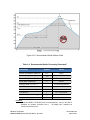
Figure 3-1 plots typical gain-determined resolution as a function of the single axis sample
rate. The plot starts at 300 Hz since the usable resolution is limited by best-case system noise
of ~15 nT. The plot stops at 2400 Hz because this represents a cycle count of ~30, and
operating at cycle counts much lower than this introduces significant quantization error.
(The number of cycle counts is determined by the user, as explained in Sections 5.1 and 6.2.)
Gain-determined Resolution (nT)
150
120
90
60
30
0
300
600
900
1200
1500
1800
2100
2400
Single-Axis Sample Rate (Hz)
Figure 3-1: Sample Rate vs. Resolution – Standard Mode
(Usable resolution will be limited by system noise at lower sample rates)
The plots below are representative of performance as a function of the number of cycle
counts, which is a parameter directly controlled by the user. The first two plots show
performance for operation in both Standard Mode and the default Legacy Mode out to 10,000
cycle counts. The maximum number of cycle counts in Legacy Mode is 4096. In Standard
Mode the maximum cycle counts is 65.5k, but there’s rarely a reason to operate in Standard
Mode much beyond 200 cycle counts, as discussed in the following paragraph.
Figure 3-4, Figure 3-5, and Figure 3-6 show performance when operating in Standard Mode
out to 200 cycle counts. Operation in Standard Mode at more than 200 cycle counts usually
is inefficient since more time and power is consumed per measurement, with diminishing
returns in usable (noise-limited) resolution.
RM3000 & RM2000 Sensor Suite User Manual – April 2011
Page 9 of 42
10000
Standard Mode
Legacy Mode (default config.)
Gain (counts/µT)
1000
100
10
1
0.1
10
100
1000
10000
Cycle Counts
Figure 3-2: Gain vs. Cycle Counts – Standard & Legacy Modes
Maximum Single-Axis Sample Rate (Hz)
(Resolution = 1/Gain, to the system’s noise limit)
10000
Standard Mode
Legacy Mode (default config.)
1000
100
10
1
10
100
1000
10000
Cycle Counts
Figure 3-3: Single-Axis Sample Rate vs. Cycle Counts – Standard & Legacy Modes
PNI Sensor Corporation
RM3000 & RM2000 Sensor Suite User Manual – April 2011
Doc #1015673 r06
Page 10 of 42
50
45
Gain (counts/µT)
40
35
30
25
20
15
10
5
0
0
20
40
60
80
100
120
140
160
180
200
Cycle Counts
Figure 3-4: Gain vs. Cycle Counts – Standard Mode
(Resolution = 1/Gain, to the system’s noise limit)
Maximum Single-Axis Sample Rate (Hz)
3000
2700
2400
2100
1800
1500
1200
900
600
300
0
0
20
40
60
80
100
120
140
160
180
200
Cycle Counts
Figure 3-5: Single-Axis Sample Rate vs. Cycle Counts – Standard Mode
RM3000 & RM2000 Sensor Suite User Manual – April 2011
Page 11 of 42
Current Consumption @ 35 Hz
Single-Axis Sample Rate (mA)
0.40
0.35
0.30
0.25
0.20
0.15
0.10
0.05
0.00
0
20
40
60
80
100
120
140
160
180
200
Cycle Counts
Figure 3-6: Current Consumption vs. Cycle Counts – Standard Mode
PNI Sensor Corporation
RM3000 & RM2000 Sensor Suite User Manual – April 2011
Doc #1015673 r06
Page 12 of 42
3.5 Dimensions and Packaging
3.5.1 Sen-XY Dimensions & Packaging
Figure 3-7: Sen-XY Sensor Dimensions
Figure 3-8: Sen-XY Solder Pad Layout
RM3000 & RM2000 Sensor Suite User Manual – April 2011
Page 13 of 42
Dimensions: mm
Full reel is 5,000 pcs. Smaller quantities on cut-tape.
Tape & Reel meets ANSI/EIA standard EIA-418-B
Figure 3-9: Sen-XY Tape and Reel Dimensions
3.5.2 Sen-Z Dimensions & Packaging
Figure 3-10: Sen-Z Sensor Dimensions
PNI Sensor Corporation
RM3000 & RM2000 Sensor Suite User Manual – April 2011
Doc #1015673 r06
Page 14 of 42
Figure 3-11: Sen-Z Solder Pad Layout
Dimensions: mm
Full reel is 1200 pcs. Smaller quantities on cut-tape.
Tape & Reel meets ANSI/EIA standard EIA-418-B
Figure 3-12: Sen-Z Tape and Reel Dimensions
RM3000 & RM2000 Sensor Suite User Manual – April 2011
Page 15 of 42
3.5.1 Sen-Z Shield Dimensions & Packaging
Figure 3-13: Sen-Z Shield Sensor Dimensions
Figure 3-14: Sen-Z Shield Solder Pad Layout
PNI Sensor Corporation
RM3000 & RM2000 Sensor Suite User Manual – April 2011
Doc #1015673 r06
Page 16 of 42
Dimensions: mm
Full reel is 600 pcs. Smaller quantities on cut-tape.
Tape & Reel meets ANSI/EIA standard EIA-418
Figure 3-15: Sen-Z Shield Tape and Reel Dimensions
3.5.2 3D MagIC Dimensions and Packaging
Figure 3-16: 3D MagIC MLF Mechanical Drawing
RM3000 & RM2000 Sensor Suite User Manual – April 2011
Page 17 of 42
Figure 3-17: 3D MagIC MLF Tape Dimensions
Figure 3-18: 3D MagIC Die Pad Layout
PNI Sensor Corporation
RM3000 & RM2000 Sensor Suite User Manual – April 2011
Doc #1015673 r06
Page 18 of 42
Figure 3-19: Example Wire Bonding Layout for Legacy 11096 ASIC Applications
Note that Figure 3-19 is for illustrative purposes only. The sample bond pad layout was
taken from a PNI product that incorporates the 3D MagIC die. The customer’s bond pad
layout will vary, as will the best layout for the customer’s application.
3.6 Soldering
Figure 3-20 and Table 3-6 provide the recommended solder reflow profile and processing
parameters for RM3000 components. After soldering PNI components to a board, it is
possible to wave solder the opposite side of the PCB.
IMPORTANT: PNI sensors require the use of halide-free solder pastes and processes for
reflow and cleaning. Please contact PNI if you would like recommendations.
RM3000 & RM2000 Sensor Suite User Manual – April 2011
Page 19 of 42
PB
Figure 3-20: Recommended Solder Reflow Profile
Table 3-6: Recommended Solder Processing Parameters1
Parameter
Symbol
Value
Preheat Temperature, Minimum
TSmin
150°C
Preheat Temperature, Maximum
TSmax
200°C
60 – 180 seconds
Preheat Time (TSmin to TSmax)
Solder Melt Temperature
TL
Ramp-Up Rate (TSmax to TL)
Peak Temperature
>218°C
3°C/second maximum
TP
Time from 25°C to Peak (TP)
<260°C
6 minutes maximum
Time above TL
tL
60 – 120 seconds
Soak Time (within 5°C of TP)
tP
10 – 20 seconds
Rampdown Rate
4°C/second maximum
Footnote:
1. Meets IPC/JEDEC J-STD-020 profile recommendations. Sen-XY and Sen-Z
classified as moisture sensitivity level 1. 3D MagIC MLF classified as
moisture sensitivity level 3.
PNI Sensor Corporation
RM3000 & RM2000 Sensor Suite User Manual – April 2011
Doc #1015673 r06
Page 20 of 42
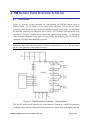
4 RM Sensor Suite Overview & Set-Up
4.1 Overview
Figure 4-1 provides a basic schematic for implementing the RM3000 Sensor Suite in
Standard Mode. The 3D MagIC is at the center of the schematic, as it ties the user’s host
controller (on the left) to the three Reference Magnetic Sensors (on the right). To implement
the RM2000, simply do not connect the Sen-Z sensor. The 3D MagIC also can operate only
one sensor if desired. Unused sensor connections should remain floating. To implement
either Reference Magnetic Sensor Suite in Legacy Mode, the Mode pin (pin #12) should be
connected to DVDD, rather than tied to ground.
Note: RM3000 and RM2000 Reference Magnetic Sensor Suites typically are used in compassing
applications, where each channel represents a Cartesian coordinate axis (x, y, or z). For this reason,
the term “axis” generally is used instead of “channel”.
Figure 4-1: RM3000 reference schematic – Standard Mode
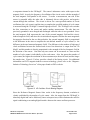
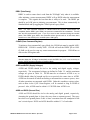
The Sen-XY and/or Sen-Z sensors serve as the inductive element in a simple LR relaxation
oscillation circuit which is composed of an external bias resistor along with digital gates and
RM3000 & RM2000 Sensor Suite User Manual – April 2011
Page 21 of 42
a comparator internal to the 3D MagIC. The sensor’s inductance varies with respect to the
magnetic field. As such, the frequency of oscillation of the circuit varies with the strength of
the total magnetic field parallel to the sensor. To make a measurement, one side of the
sensor is grounded while the other side is alternately driven with positive and negative
current through the oscillator. The circuit is driven for a user-specified number of circuit
oscillations (the cycle counts), and the time to complete the specified number of cycle counts
is measured using the 3D MagIC’s internal high-speed clock. The 3D MagIC next switches
the bias connection to the sensor and makes another measurement. The side that was
previously grounded is now charged and discharged while the other is now grounded. Since
the total magnetic field represents the sum of the external magnetic field and the circuitinduced magnetic field, and since the circuit-induced magnetic field has the same magnitude
but opposite direction for the two bias polarities, the external magnetic field is proportional
to the difference in the time to complete the user-defined number of cycle counts (i.e. the
difference in the total measured magnetic field). The difference in the number of high-speed
clock oscillations between the forward and reverse bias directions is output from the 3D
MagIC, and this number is directly proportional to the strength of the local magnetic field in
the direction of the sensor. Note that only one sensor can be measured at a time and the
number of cycle counts is individually set for each sensor. Also, the greater the number of
cycle counts, the higher the resolution of the measurement (to the noise limit) and the longer
the sample time. Figure 4-2, below, provides a detail of the biasing circuit. For additional
information on PNI’s magneto-inductive sensor technology, please refer to the “MagnetoInductive Technology Overview” white paper found on PNI’s website.
Figure 4-2: LR Oscillator Circuit Biasing Diagram
Since the Reference Magnetic Sensor Suite works in the frequency domain, resolution is
cleanly established by the number of cycle counts. Also, the output from the 3D MagIC is
inherently digital and can be fed directly into a microprocessor, which eliminates the need for
signal conditioning or an analog/digital interface between the sensor and host processor.
PNI Sensor Corporation
RM3000 & RM2000 Sensor Suite User Manual – April 2011
Doc #1015673 r06
Page 22 of 42
4.2 Layout
4.2.1 Sensor Orientation
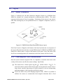
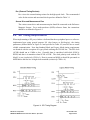
Figure 4-3 indicates how the three Reference Magnetic Sensors in a RM3000 Suite
should be oriented for a system referenced as north-east-down (NED). The arrow
represents the direction of travel or pointing. Positioning of the sensors is not critical,
other than ensuring they are not positioned close to a magnetic component, such as a
speaker.
Figure 4-3: RM3000 North-East-Down (NED) Sensor Layout
If the Sen-Z sensor is flipped to the bottom of the board such that the curved portion of
the sensor still points forward, then to retain NED the Sen-Z’s ZDRVN and ZDRVP pads
should be as shown above, except on the bottom of the board. Since the pads on the
Sen-Z have switched positions, the connections to the Sen-Z sensor will be reversed.
4.2.2 Local Magnetic Field Considerations
Since the sensors measure magnetic field, it is important to consider what items in the
vicinity of the sensors can affect the sensor readings. Specifically:
The sensors have a linear regime of 200 T. (Earth’s field is ~50 T.) To
ensure the sensors operate in their linear regime, do not place the sensors close to
large electric currents, large masses of ferrous material, or devices incorporating
permanent magnets, such as speakers and electric motors.
Locate the sensors away from changing magnetic fields. While it is possible to
calibrate the sensors to accommodate local magnetic distortion that is fixed
RM3000 & RM2000 Sensor Suite User Manual – April 2011
Page 23 of 42
relative to the sensors, changing local magnetic fields generally cannot be
accommodated. When the local magnetic field will change, try to take readings
only when the field is in a known state. For instance, if a motor will be running
part of the time, take readings only when the motor is in a known state (e.g. off).
If you are uncertain about the effect a specific component may have on the
system, the RM3000 Evaluation Board can be used to help ascertain this. Place
the RM3000 Evaluation Board on a firm surface and gradually bring the
component in question close to the board, then note when the magnetic field starts
to change. If the component cannot be moved, then gradually move the RM3000
Evaluation Board towards the component; however it is necessary to ensure the
orientation of the board remains constant while doing this. If an RM3000
Evaluation Board is not available, gradually bring the component in question
closer to one of the Reference Magnetic Sensors and observe when the sensor
reading starts to change. Note that the affect of a local magnetic distortion drops
3
off as 1/distance .
4.2.3 Other Layout Considerations
Other design considerations include:
To minimize the effect of gradients in the magnetic field, position the sensors as
close to each other as possible.
To reduce coupling to and from other signals, keep the two traces from the 3D
MagIC to each sensor as close as possible to each other. (The 3D MagIC can be
located up to 0.5 m away from the sensors.)
Keep capacitors (especially tantalum capacitors) far away from the sensors.
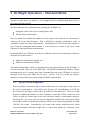
4.3 3D MagIC Pin-Out
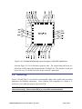
The 3D MagIC’s pin-out is summarized in Table 4-1. Pin numbers run counterclockwise
(when looking from the top), starting at the Pin 1 designator as shown in Figure 3-16.
PNI Sensor Corporation
RM3000 & RM2000 Sensor Suite User Manual – April 2011
Doc #1015673 r06
Page 24 of 42
Table 4-1: 3D MagIC Pin Assignments
MLF
Pin#
Die
Pad#
Pin
Name
Description
SPI interface – Master Output, Slave Input Serial Data
1
1
MOSI
2
2
NC
3
3
SSN
SPI interface – Active low to select port
4
4
AVDD
Supply voltage for analog section of ASIC
5
5
AVSS
Ground pin for analog section of ASIC
6
6
ZDRVP
Z sensor drive output
7
7
ZINP
Z sensor measurement input
8
8
ZINN
Z sensor measurement input
9
9
ZDRVN
Z sensor drive output
10
10
YDRVP
Y sensor drive output
11
11
YINP
12
12
MODE
13
13
YINN
14
14
YDRVN
Y sensor drive output
15
15
XDRVP
X sensor drive output
16
16
XINP
X sensor measurement input
17
17
XINN
X sensor measurement input
18
18
XDRVN
X sensor drive output
19
19
DVSS
Ground pin for digital section of ASIC
--
20
NC
Do not connect
20
21
NC
Do not connect
21
22
NC
Do not connect
22
23
CLEAR
Clear Command Register
23
24
DRDY
Data ready command
24
25
NC
Do not connect
25
26
REXT
External timing resistor for high speed clock.
26
27
DVDD
Supply voltage for digital section of ASIC.
27
28
SCLK
SPI interface - Serial clock input
28
29
MISO
SPI interface – Master Input, Slave Output
Do not connect
Y sensor measurement input
Mode Select: tie to DVSS for Standard, DVDD for Legacy
Y sensor measurement input
RM3000 & RM2000 Sensor Suite User Manual – April 2011
Page 25 of 42
MODE
The MODE pin establishes whether communication with the 3D MagIC will comply
with Standard Mode protocol (see Section 5) or Legacy Mode protocol (see Section
6). The MODE pin should be grounded (connected to DVSS) to operate in Standard
Mode, and set HIGH (connected to DVDD) to operate in Legacy Mode.
SCLK (SPI Serial Clock Input)
SCLK is a SPI input used to synchronize the data sent in and out through the MISO
and MOSI pins. SCLK is generated by the customer-supplied master device and
should be 1 MHz or less. One byte of data is exchanged over eight clock cycles.
Data is captured by the master device on the rising edge of SCLK. Data is shifted out
and presented to the 3D MagIC on the MOSI pin on the falling edge of SCLK, except
for the first bit (MSB) which must be present before the first rising edge of SCLK.
SSN (SPI Slave Select)
This signal sets the 3D MagIC as the operating slave device on the SPI bus. The SSN
pin must be LOW prior to data transfer in either direction, and must stay LOW during
the entire transfer.
The SSN pin must transition from HIGH to LOW prior to initiating a multi-axis
measurement (MAM) command and prior to reading or writing to the Cycle Count
Register or Clock Divide Register. It must stay LOW for the remainder of the
operation.
After communication between the 3D MagIC and master device is finished, the SPI
bus can be freed up (SSN pin set HIGH) to communicate with other slave devices
while the 3D MagIC takes a measurement or is idle.
MISO (SPI Serial Out)
MISO is a SPI output that sends data from the 3D MagIC to the master device. Data
is transferred most significant bit first and is captured by the master device on the
rising edge of SCLK. The MISO pin is placed in a high impedance state if the 3D
MagIC is not selected (i.e. if SSN=1).
MOSI (SPI Serial In)
MOSI is a SPI input that provides data from the master device to the 3D MagIC.
Data is transferred most significant bit first. Data must be presented at least 50 ns
before the rising edge of SCLK, and remain valid for 50 ns after the edge. New data
typically is presented to the MOSI pin on the falling edge of SCLK.
PNI Sensor Corporation
RM3000 & RM2000 Sensor Suite User Manual – April 2011
Doc #1015673 r06
Page 26 of 42
DRDY (Data Ready)
DRDY is used to ensure data is read from the 3D MagIC only when it is available.
After initiating a sensor measurement, DRDY will go HIGH when the measurement
is complete. This signals the host that data is ready to be read. The DRDY pin
should be set LOW prior to initiating a measurement. This is done automatically in
Standard Mode and by toggling the CLEAR pin in Legacy Mode.
Note: If a new command sequence is started before the previous measurement has
completed (before DRDY goes HIGH), the previous command will be overwritten. This will
also stop the measurement cycle. If you try to send a new command during the readout
phase, after DRDY goes HIGH, the command will be ignored until all 16 bits have been
clocked our or the CLEAR pin is set HIGH (then LOW again).
CLEAR (Clear Command Register)
To initiate a clear command in Legacy Mode, the CLEAR pin must be toggled LOWHIGH-LOW. CLEAR is usually LOW. CLEAR will reset the DRDY pin to LOW.
CLEAR can be used to stop any sensor measurement in progress. CLEAR has no
effect on the SPI register state.
Note: The CLEAR pin is similar to the RESET pin on PNI’s legacy ASIC. However in
Standard Mode the 3D MagIC automatically resets the DRDY line, so it is not necessary to
use the CLEAR pin when operating in Standard Mode.
AVDD and DVDD (Supply Voltages)
AVDD and DVDD should be tied to the analog and digital supply voltages,
respectively. The recommend voltages are defined in Table 3-5, and the maximum
voltages are given in Table 3-4. DVDD must be on whenever AVDD is on, so
DVDD should either be brought up first or at precisely the same time as AVDD.
AVDD can be turned off when not making a measurement to conserve power, since
all other operations are supported with DVDD. Under this condition, register values,
such as those in the Cycle Count Register, will be retained as long as DVDD is
powered. Also, AVDD must be within 0.1 V DVDD when AVDD is on.
AVSS and DVSS (Ground Pins)
AVSS and DVSS should be tied to the analog and digital ground, respectively.
Assuming the ground plane is clean, they may share a common ground. They may
have their own ground planes if this is more convenient from the standpoint of the
user’s circuit layout. DVSS and AVSS should be within 0.1 V of each other.
RM3000 & RM2000 Sensor Suite User Manual – April 2011
Page 27 of 42
REXT (External Timing Resistor)
REXT ties to the external timing resistor for the high-speed clock. The recommended
value for the resistor and associated clock speed are defined in Table 3-1.
Sensor Drive and Measurement Pins
The various sensor drive and measurement pins should be connected to the Reference
Magnetic Sensors. For a north-east-down (NED) reference frame, the connections
should be as defined in Figure 4-3.
4.4 SPI Timing Requirements
When implementing a SPI port, whether a dedicated hardware peripheral port or a softwareimplemented port using general purpose I/O (also known as Bit-Banging), the timing
parameters (defined below in Figure 4-4 and specified in Table 4-2) must be met to ensure
reliable communication. Note that Standard Mode and Legacy Mode timing requirements
are identical with the exception of Legacy Mode utilizing the CLEAR line. The SPI clock
(SCLK) should run at 1 MHz or less. Generally data is considered valid while SCLK is
HIGH, and data is in transition when SCLK is LOW. The clock polarity used with the 3D
MagIC is zero (exclusively CPOL=0). Data is present on MISO or should be presented on
MOSI before the first low to high clock transition (exclusively CPHA = 0).
Figure 4-4: SPI Timing Diagram
PNI Sensor Corporation
RM3000 & RM2000 Sensor Suite User Manual – April 2011
Doc #1015673 r06
Page 28 of 42
Table 4-2: SPI Timing Specifications
Symbol
Description
Min
Time from SSN to CLEAR
10
ns
tCMIN
CLEAR duration
100
ns
tSSDV
Time from SSN to Command Byte on MOSI
1
us
tDBSH
Time to setup data before active edge
50
ns
tDASH
Time to setup data after active edge
50
ns
tSHDZ
Time from SSN to data tri-state time
tSC
Max
100
Units
ns
4.5 Idle Mode
The 3D MagIC incorporates an Idle Mode to reduce power consumption, in which the circuit
automatically idles when it is not exchanging data or taking a measurement. The 3D MagIC
starts in the Idle Mode at power-up and remains in Idle Mode until a measurement is needed.
Note: The 3D MagIC starts in Idle Mode when powered on. This is different from the legacy 11096
ASIC, which required cycling through one measurement request operation to put it into Idle Mode.
RM3000 & RM2000 Sensor Suite User Manual – April 2011
Page 29 of 42
5 3D MagIC Operation – Standard Mode
Note: This section discusses how to operate the 3D MagIC in Standard Mode. For a description of
operation in Legacy Mode, see Section 6. The 3D MagIC operates in Standard Mode when pin #12 is
held LOW (grounded to DVSS).
The basic functions to be performed when operating the 3D MagIC are:
Setting the values in the Cycle Count Registers, and
Taking sensor measurements.
The user should first establish the number of cycle counts to be measured for each sensor by
writing to the Cycle Count Registers. This is followed by sending a command or series of
commands to make the sensor measurements. Assuming the user will use the same number of
cycle counts for subsequent measurements, it is not necessary to rewrite to the Cycle Count
Registers for subsequent sensor measurements.
In Standard Mode, the 3D MagIC provides two methods to take sensor measurements, which are
discussed later in this section:
Single-axis measurement (SAM), and
Multi-axis measurement (MAM).
The SAM Command Byte initiates a measurement for one sensor and sets up the 3D MagIC to
write the measured values out on the MISO line. The MAM Command Byte initiates a sensor
measurement for up to 3 sensors, and a later Command Byte sets up the 3D MagIC to write the
measured values out on the MISO line for up to 3 sensors. For two or three axis systems,
normally it is more efficient to operate using the MAM Command Byte.
5.1 Cycle Count Registers
Prior to sending a command to take a sensor measurement, it is necessary to write values to
the Cycle Count Registers. (The default value for the Cycle Count Registers is 512D, but
this was chosen for legacy reasons and is an inefficient value otherwise.) The Cycle Count
Registers establish the number of sensor oscillation cycles that will be counted for each
sensor in both the forward and reverse bias directions during a measurement sequence.
Increasing the cycle count value increases measurement resolution, but system noise limits
the useable resolution such that the maximum efficient cycle count value generally is around
200-300 cycle counts. Lowering the cycle count value reduces acquisition time, which
increases maximum achievable sample rate or, with a fixed sample rate, decreases power
PNI Sensor Corporation
RM3000 & RM2000 Sensor Suite User Manual – April 2011
Doc #1015673 r06
Page 30 of 42
consumption. See Figure 3-4, Figure 3-5, and Figure 3-6 to estimate the appropriate cycle
count value for your application. Once the Cycle Count Registers are set, they do not need to
be repopulated unless the user wants to change the values or the system is powered down (in
which case the default values would populate the register fields when powered up again).
To initiate a read to or write from the Cycle Count Register, the command byte is defined as:
Bit #
7
6
5
4
Value
1
R/W
0
0
3
2
1
0
ADR3 ADR2 ADR1 ADR0
R/W: Read/Write
HIGH signifies a Read operation from the addressed register. LOW signifies a Write
operation to the addressed register.
ADR0 – ADR3: Register Address Bits
Establishes which register will be written to or read from. Each sensor is represented
by two registers, with addresses defined as follows:
Table 5-1: Cycle Count Register Commands
Read Command
Byte
Write Command
Byte
X Axis Cycle Count Value - MSB
C3H
83H
X Axis Cycle Count Value - LSB
C4H
84H
Y Axis Cycle Count Value - MSB
C5H
85H
Y Axis Cycle Count Value - LSB
C6H
86H
Z Axis Cycle Count Value - MSB
C7H
87H
Z Axis Cycle Count Value - LSB
C8H
88H
Register Description
Since the registers are adjacent, it is not necessary to send multiple Command Bytes, as the
3D MagIC automatically will read/write to the next adjacent register.
A sample command sequence is provided below which sets the cycle count value to 100D
(64H) for all 3 axes. This is purely for illustrative purposes and the value could be different
and/or the number of axes to be addressed could be different.
Start with SSN set HIGH, then set SSN to LOW.
Send 83H (this is the Write Command Byte to address the MSB for the X axis)
RM3000 & RM2000 Sensor Suite User Manual – April 2011
Page 31 of 42
Send 0 (value for the MSB for the X axis)
Send 64H (value for the LSB for the X axis - pointer automatically increments)
Send 0 (value for the MSB for the Y axis - pointer automatically increments)
Send 64H (value for the LSB for the Y axis - pointer automatically increments)
Send 0 (value for the MSB for the Z axis - pointer automatically increments)
Send 64H (value for the LSB for the Z axis - pointer automatically increments)
Set SSN to HIGH
5.2 Single-Axis Measurement (SAM) Operation
The SAM Command Byte initiates a sensor measurement on a single sensor, and sets up the
3D MagIC to output the measured values on the MISO line. Generally SAM operation is not
as efficient as MAM operation, except when only one sensor (in total) is to be measured.
5.2.1 SAM SPI Activity Sequence
The SPI activity sequence for SAM operation is given below. SPI timing is discussed in
Section 4.4. The Return Byte is 9AH. Three (3) data bytes will be clocked out for a
single-axis measurement. The Command Byte is discussed below.
Figure 5-1: SPI Activity Sequence Diagram for SAM Operation
PNI Sensor Corporation
RM3000 & RM2000 Sensor Suite User Manual – April 2011
Doc #1015673 r06
Page 32 of 42
5.2.2 SAM Command Byte
The SAM Command Byte is defined as follows:
Bit #
7
6
5
4
3
2
Value
0
0
0
0
0
0
1
0
AS1 AS0
Table 5-2: SAM Axis Select Bits
Axis Measured
AS1
AS0
No axis measured
0
0
X axis
0
1
Y axis
1
0
Z axis
1
1
5.2.3 Making a Single-Axis Measurement
The steps to make a single-axis sensor measurement are given below. The 3D MagIC
will return the result of a complete forward- reverse measurement of the sensor in a 24 bit
2’s complement format (range: -8388608 to 8388607).
SSN pin is set LOW. This enables communication with the master device.
The SAM Command Byte is clocked into the 3D MagIC on the MOSI pin.
Simultaneously, the 3D MagIC will present a fixed 9AH on the MISO pin. Once
the 8 bits have clocked in, the 3D MagIC will execute the command (i.e. take a
measurement).
The SSN input may be returned HIGH at this point to free up host communication
with another device if desired. This will not affect the measurement process.
A measurement is taken.
At the end of the measurement, the DRDY pin is set HIGH, indicating data is
ready, and the 3D MagIC is placed in Idle Mode.
The SSN input should be set LOW, if it is not already, to read the data.
The data is clocked out on the MISO pin with the next 24 clock cycles.
If another measurement is immediately made, SSN can remain LOW and the process
repeated. Otherwise it is recommended that SSN is set HIGH to release the SPI bus.
RM3000 & RM2000 Sensor Suite User Manual – April 2011
Page 33 of 42
5.3 Multi-Axis Measurement (MAM) Operation
An initial MAM Command Byte initiates a sensor measurement for up to 3 sensors. After
the measurements are made and the DRDY line goes HIGH, another MAM Command Byte
sets up the 3D MagIC to output the measured values on the MISO line.
5.3.1 MAM SPI Activity Sequence
The SPI timing sequence is given below for MAM operation. SPI timing is discussed in
Section 4.4. The Return Byte is 9AH. The number of data bytes will be determined by
the number of axes that are to be measured. Each axis is comprised of 3 bytes of data, so
for a 3 axis measurement 9 total bytes would be clocked out to receive all the data. The
Command Byte and Axes Select Byte are discussed below.
Figure 5-2: SPI Activity Sequence Diagram for MAM Operation
5.3.2 MAM Command Byte
The MAM Command Byte either initiates a sensor measurement or initiates placing the
measurement results on the MISO line for the host to read. The MAM Command Byte is
82H to initiate a sensor measurement and is C9H to retrieve the data.
Note: Measurement results are stored in registers within the 3D MagIC. If SCLK continues to run
after the appropriate number of data bytes for the defined number of axes to be measured, then
the information on the MISO line will have little meaning. SCLK should be stopped once the
measurements are clocked out.
PNI Sensor Corporation
RM3000 & RM2000 Sensor Suite User Manual – April 2011
Doc #1015673 r06
Page 34 of 42
5.3.3 MAM Axes Select Byte
The MAM Axes Select Byte establishes which axes are to be measured and is defined as
follows:
Bit #
7
6
5
Value
0
0
0
4
3
AAX1 AAX0
2
1
0
0
0
1
Table 5-3: MAM Axes Select Bits
Axes Measured
AAX1
AAX0
X, Y, and Z
0
0
X and Y
0
1
X only
1
0
No axis measured
1
1
5.3.4 Making a Multi-Axis Measurement
The steps to make a multi-axis sensor measurement are given below. The 3D MagIC will
return the result of a complete forward- reverse measurement of each sensor in a 24 bit
2’s complement format (range: -8388608 to 8388607).
Start with SSN set HIGH, then set SSN to LOW.
Initiate a sensor measurement by sending 82H (MAM Command Byte to write to
the Mode Register) followed by 01H (Mode Register Word to initiate
measurement) on the MOSI pin. The 3D MagIC will now take the prescribed
measurements.
Return SSN to HIGH. This will not affect the measurement process, but will free
up the host to communicate with other devices and ensure the next Command
Byte sent to the 3D MagIC is interpreted properly.
A measurement is taken.
At the end of the measurement, the DRDY pin is set HIGH, indicating data is
ready, and the 3D MagIC is placed in Idle Mode.
When the host is ready to read the measured values, set SSN to LOW. If SSN
already is LOW, then toggle SSN from LOW to HIGH to LOW.
RM3000 & RM2000 Sensor Suite User Manual – April 2011
Page 35 of 42
Send C9H (MAM Command Byte to read from the ) on the MOSI pin to initiate
reading the measurement values. Data is clocked out on the MISO pin. Each
sensor reading consists of 3 bytes of data, clocked out MSB first. X-axis data is
presented first, then y-axis data, then z-axis data. The first nine (9) bytes
represent a complete 3-axis measurement.
Return SSN to HIGH to free up the host to communicate with other devices and
to ensure the next Command Byte sent to the 3D MagIC is interpreted properly.
PNI Sensor Corporation
RM3000 & RM2000 Sensor Suite User Manual – April 2011
Doc #1015673 r06
Page 36 of 42
6 3D MagIC Operation – Legacy Mode
Note: This section discusses how to operate the 3D MagIC in Legacy Mode. For a description of
operation in Standard Mode, see Section 5. The 3D MagIC will operate in Legacy Mode when pin #12 is
held HIGH (connected to DVDD).
The intent of Legacy Mode is to enable the user to easily substitute PNI’s 3D MagIC for PNI’s
legacy 11096 ASIC (p/n 12576).
If the user wishes to simply duplicate the performance of the 11096 ASIC (Legacy Operation),
then a measurement is made by sending the Legacy Command Byte. This command byte is the
same as for the 11096 ASIC. The Legacy Command Byte initiates a sensor measurement on a
single sensor, and sets up the 3D MagIC to output the measured values on the MISO line.
Legacy Operation is covered in Section 6.1
If the user wishes to derive the lower power consumption advantages of the 3D MagIC and is
willing to make some code changes but cannot make hardware changes, then Enhanced Legacy
Operation allows for this. (If the user can make both code and hardware changes, then operation
in Standard Mode is recommended.) For Enhanced Legacy Operation, the user first will write to
the Clock Divide Register and after this follow the same process as for Legacy Operation.
Please review both Sections 6.1 and 6.2, as Section 6.1 still applies and Section 6.2 covers the
additional steps required for Enhanced Legacy Operation.
6.1 Legacy Operation
In Legacy Mode a sensor measurement is initiated with the Legacy Command Byte, and this
command also sets up the 3D MagIC to output measurement data on the MISO line once this
data becomes available.
Note the 3D MagIC’s high-speed clock runs at nominally 45 MHz, but the 11096 ASIC runs
at nominally 2 MHz. Consequently, when the 3D MagIC is in default Legacy Mode, the
clock speed is divided by 16 thus reducing the clock speed to 2.8 MHz. At an effective clock
speed of 2.8 MHz the gain of the 3D MagIC circuit will closely match the gain of the 11096
ASIC circuit operating at 2 MHz. (The effective clock speed of the 3D MagIC is not 2 MHz
for gain matching because of differences in the circuit oscillation frequency between the 3D
MagIC and the 11096 ASIC circuits.) As such, the performance of the 3D MagIC closely
matchs that of the 11096 ASIC circuit with no software coding or hardware changes on the
user’s part. But performance is sub-optimized, and specifically power consumption can be
reduced by up to 90% with software changes on the user’s part, as discussed in Section 6.2.
RM3000 & RM2000 Sensor Suite User Manual – April 2011
Page 37 of 42
6.1.1 Legacy Operation SPI Activity Sequence
The SPI activity sequence is given below for Legacy operation. SPI timing is discussed
in Section 4.4. The Return Byte is 9BH. Two (2) data bytes will be clocked out for a
Legacy measurement. The Command Byte is discussed below.
Figure 6-1: SPI Activity Sequence Diagram for Legacy Operation
6.1.2 Legacy Command Byte
The command byte to initiate a sensor measurement is defined as follows:
Bit #
7
Value
0
6
5
4
PS2 PS1 PS0
3
2
0
0
1
0
AS1 AS0
PS0-PS2: Period Select
Selects the number of sensor circuit oscillation cycles (cycle counts) to be counted
while simultaneously using the internal fixed reference clock to measure the time to
obtain this count.
PNI Sensor Corporation
RM3000 & RM2000 Sensor Suite User Manual – April 2011
Doc #1015673 r06
Page 38 of 42
Table 6-1: Legacy Period Select Bits
Period Select Value
Cycle Counts
PS2
PS1
PS0
0
32
0
0
0
1
64
0
0
1
2
128
0
1
0
3
256
0
1
1
4
512
1
0
0
5
1024
1
0
1
6
2048
1
1
0
7
4096
1
1
1
AS0-AS1: Axis Select
Determines the sensor to be measured.
Table 6-2: Legacy Axis Select Bits
Axis Measured
AS1
AS0
No axis measured
0
0
X axis
0
1
Y axis
1
0
Z axis
1
1
6.1.3 Making a Legacy Measurement
The steps to make a sensor measurement are given below. In Legacy Mode, the 3D
MagIC returns the result of a complete forward- reverse measurement of the sensor in a
16 bit 2’s complement format (range: -32768 to 32767). Note this is different from
Standard Mode, where a 24 bit value is returned.
SSN pin is set LOW. (This enables communication with the master device.)
CLEAR pin is set HIGH, then LOW. This is not required, but is optional to
maintain compatibility with the legacy 11096 ASIC.
A command byte is clocked into the 3D MagIC on the MOSI pin. Simultaneously,
the 3D MagIC will present a fixed 9BH on the MISO pin. Once the 8 bits have
clocked in, the 3D MagIC will execute the command (i.e. take a measurement).
RM3000 & RM2000 Sensor Suite User Manual – April 2011
Page 39 of 42
The SSN input may be returned HIGH at this point to free up host communication
with another device if desired. This will not affect the measurement process.
A measurement is taken, which consists of forward biasing the sensor and making
a period count; then reverse biasing the sensor and counting again; and then
taking the difference between the two directions and presenting this value.
At the end of the measurement, the DRDY pin is set HIGH, indicating data is
ready, and the 3D MagIC is placed in Idle Mode.
The SSN input should be set LOW, if it is not already, to read the data.
The data is clocked out on the MISO pin with the next 16 clock cycles.
If another measurement is to be made immediately, the SSN pin can remain low and the
process repeated. Otherwise, it generally is recommended to set the SSN pin HIGH to
release the SPI serial bus.
6.2 Enhanced Legacy Operation
Note: Enhanced Legacy Operation involves improving performance of a legacy system by
implementing only software changes. If the user can make both software and hardware changes,
then operation in Standard Mode is recommended as it allows for multi-axis measurement operation
and finer granularity in establishing the number of cycle counts.
The 3D MagIC incorporates a Clock Divide Register that effectively divides the 3D MagIC’s
high-speed internal clock by some integer value (Clock Divide Value). In Legacy Mode the
default is 16 as this results in performance matching that of the 11096 ASIC at similar Period
Select values. But for the most efficient operation, the value should be 1 since this gives the
greatest time-based resolution. If a legacy user cannot set pin #12 to DVSS to operate in
Standard Mode, but can make code changes, it is possible to significantly reduce power
consumption (see Table 6-4) by over-writing the Legacy Mode default Clock Divide Value
and using a smaller Period Select value. In this case, the user first will write to the Clock
Divide Register and after this follow the same process as for Legacy Operation, except with a
different Period Select value.
For example, if a user operates in default Legacy Mode and sets the Period Select value to 5,
the cycle count will be 1024 and the effective clock speed with be ~2.8 MHz. By changing
the Clock Divide value from 16 (Legacy Mode default) to 1, the effective clock speed
increases to ~45 MHz. With this significantly higher clock speed, the Period Select value
can be reduced to 1 (64 cycle counts) such that the gain remains unchanged but the time to
take the measurement, and hence power consumption, is dramatically reduced.
PNI Sensor Corporation
RM3000 & RM2000 Sensor Suite User Manual – April 2011
Doc #1015673 r06
Page 40 of 42
6.2.1 Clock Divide Command Byte
The Command Byte to initiate reading or writing to the Clock Divide Register is defined
as follows:
Bit #
7
6
5
4
3
2
1
0
Value
1
R/W
0
0
0
0
0
0
R/W: Read/Write
When HIGH signifies a Read operation from the Clock Divide Register. When LOW
signifies a Write operation to the Clock Divide Register.
6.2.2 Clock Divide Register
The Clock Divide Register is defined as follows:
Bit #
7
6
5
4
3
Value
0
0
0
0
0
2
1
0
CD2 CD1 CD0
Table 6-3: Clock Divide Bits
Clock Divide Value
CD2
CD1
CD0
1
(Standard Mode default)
0
0
0
2
0
0
1
4
0
1
0
8
0
1
1
16
(Legacy Mode default)
1
0
0
16
1
0
1
16
1
1
0
16
1
1
1
RM3000 & RM2000 Sensor Suite User Manual – April 2011
Page 41 of 42
6.2.3 Command Sequence for Setting Clock Divide Value
A sample command sequence is given below which sets the Clock Divide Value to “1”.
Set SSN to LOW.
Send 80H (this is the Command Byte to write to the Clock Divide Register)
Send 0 (this sets the Clock Divide Value to “1”)
Set SSN to HIGH
6.2.4 Changes to the Period Select Value
Since the high-speed clock is running faster, the time resolution of the measurement is
increased. Consequently, the number of cycle counts required to achieve a desired
magnetic field resolution is substantially reduced, and the Period Select value in the
Legacy Command Byte should be altered. Generally speaking, the best performance will
be obtained with the Clock Divide Value set to 1.
Table 6-4: Enhanced Legacy Mode with CD = 1
Default Legacy
Enhanced Legacy with CD = 1
Period
Select
Cycle
Counts
Equivalent1
Period Select
Cycle
Counts
Power
Consumption
Gain
0
32
0
32
same
16x greater
1
64
0
32
~40% reduction
8x greater
2
128
0
32
~65% reduction
4x greater
3
256
0
32
~80% reduction
2x greater
4
512
1
64
~90% reduction
Same
5
1024
2
128
~90% reduction
Same
6
2048
3
256
~90% reduction
Same
7
4096
4
512
~90% reduction
Same
Footnote:
1. Equivalent Period Select is defined as the Period Select Value that provides equivalent gain to
the default Legacy Mode. If the Equivalent Period Select Value cannot be reduced (i.e. is at 0),
then the improvement in Gain is shown.
PNI Sensor Corporation
RM3000 & RM2000 Sensor Suite User Manual – April 2011
Doc #1015673 r06
Page 42 of 42