1
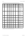
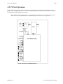
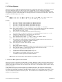
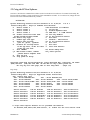
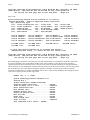
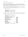
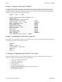
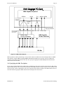
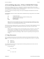
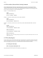
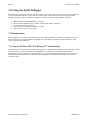
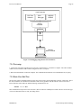
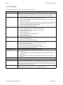
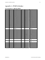
PCCtest 250/270/273/370/373 User’s Manual M200006-08 December 2002 Preliminary Sycard Technology 1180-F Miraloma Way Sunnyvale, CA 94085 (408) 749-0130 (408) 749-1323 FAX http://www.sycard.com PCCtest User’s Manual Page 1 1.0 Introduction The PCCtest 2xx and 3xx series of PC Card socket testers is designed to provide manufacturers of PC Card based hosts a quick method of testing and verifying the operation of PC Card sockets. The PCCtest 2xx and 3xx socket testers are 16-bit PC Cards. They are designed to test the sockets 16-bit interface. The PCCtest unit is a Type II PC Card that plugs into a standard Type II or III socket. The test unit is designed for both automated GO/NO-GO testing and component level debug. Test software resides on both the host PC and PCCtest unit. Simple command line invocation allows tests to be embedded into batch test files. An on-board microcontroller provides the intelligence for the PCCtest unit. The microcontroller is responsible for verifying I/O signals and also provides test stimulus to the PC card socket. The microcontroller can determine the type of error and can even narrow the error down to a specific pin or group of pins. The PCCtest contains an on-board A/D to provide accurate measurement of VCC and VPP voltages. A digital audio test provides a standard 1KHz tone to test the audio function when the PC card is configured for I/O mode. PCCtest is compatible with any Type II or III socket designed to support the PCMCIA Release 2.1 or higher standard. Software included with the PCCtest unit supports a wide variety of socket controllers based on the Intel 82365SL or Databook architecture. The latest release of the software supports a wide variety of PCI based socket controllers including CardBus controllers. For other socket controller architectures, Sycard Technology can provide technical documentation describing how to create custom test programs for the PCCtest series of socket controllers. 1.1 The PCCtest Models Sycard Technology supplies several different configurations of the PCCtest socket tester for various test needs. The different models test various levels of PC Card compliance. PCCtest 250 PCCtest 350 PCCtest 230 & PCCtest 260 PCCtest 360 PCCtest 270 Release 2.1 compliant tester. Designed for 5.0V sockets that comply with PCMCIA Release 2.1 specification. Can also be used for PC Card ‘95 based designs that do not support 3.3V or DMA. Same as the Model 250 with the addition of a debug serial port. Similar to the Model 250 but with the addition of DMA support. PCCtest 373 Similar to the Model 260 with the addition of a debug serial port. PCMCIA Release 5.0 compliant tester. Designed for mixed voltage sockets (3.3/5.0V) that comply with the PC Card specification. Supports DMA testing and voltage sense (VS1#, VS2#) testing. Same as Model 270, but with serial debug port. Same as the Model 270, but without the capability to test card detects. For use with socket controllers that turn remove power from card socket when card detects are de-asserted. The PCCtest 273 may be used to test the 16-bit interface of CardBus controllers Same as Model 273 with the addition of a debug serial port. M200006-08 1994-2002 Sycard Technology PCCtest 370 PCCtest 273 Page 2 PCCtest User’s Manual The following table summarizes the various PCCtest models and the feature sets for each: Model Support DMA 3.3V VS Pins No Card Detect No Serial Port Debug No 230 Release 2.1 No No 250 Release 2.1 No No No Yes No 350 Release 2.1 No No No Yes Yes 260 Release 2.1 Yes No No Yes No 360 Release 2.1 Yes No No Yes Yes 270 Release 2.1 and above Yes Yes Yes Yes No 370 Release 2.1 and above Yes Yes Yes Yes Yes 273 Release 2.1 and above Yes Yes Yes No No 373 Release 2.1 and above Yes Yes Yes No Yes Recommended Socket Controllers Vadem VG-230 and 5V implementations of the VG-469 5 volt implementations of Intel 82365SL, Vadem VG365/465/468, Ricoh RF5C266/366/296/396 Cirrus Logic 6710/20/22/29/30 Databook 86082 5 volt implementations of Intel 82365SL, Vadem VG365/465/468, Ricoh RF5C266/366/296/396 Cirrus Logic 6710/20/22/29/30 Databook 86082 5 Volt implementations of VLSI 82C146A, Omega 82C722, Cirrus 6722 5 volt implementations of VLSI 82C146A, Omega 82C722, Cirrus 6722 Cirrus PD6722/29/30 Ricoh RF5C296/396 VLSI 82C146A, TI PCI1050/1060 Cirrus PD6722/29/30 Ricoh RF5C296/396 VLSI 82C146A, TI PCI1050/1060 Vadem VG-469, CardBus Controllers, TI PCI-1031 Vadem VG-469, CardBus Controllers, TI PCI-1031 Table 1.1-1 PCCtest model matrix * Contact factory for information on Vadem VG-469 support. 1994-2002 Sycard Technology M200006-08 PCCtest User Manual Page 3 1.2 Compatibility PCCtest has been designed to be compatible with a wide variety of host socket controllers. Host test software is compatible with most PC compatible machines. The current software supports the following socket controllers: • • • • • • • • • • • • • • • • • All Intel 16-bit Socket Controllers All Vadem Single and dual slot socket controllers All Cirrus Logic/Basis/Intel 16b-ti Single/Dual socket controller Cirrus Logic/Basis/Intel CL-PD6832/6833/6834 CardBus Controller ** All Ricoh 16-bit PC Card socket controller Ricoh RF5C466 Dual socket CardBus - PCI Interface** Ricoh RF5C465/475 Single socket CardBus - PCI Interface ** Ricoh RF5C476/478 Dual socket CardBus - PCI Interface ** VLSI Technology 82C146/82C146A socket controllers Omega Micro 82C365G/82C722G/92C094 Dual socket controllers Omega/Trident 82C196 Dual socket CardBus controller - PCI Interface TI PCI1050/1031 – PC Card-16 PCI Interface All TI CardBus controllers ** All O2 Micro CardBus controller ** All ENE CardBus controllers ** Databook DB86082A Dual socket controller Other socket controllers fully compatible with the Intel 82365SL ** The PCCtest 2xx and 3xx support testing of the 16-bit portion of the CardBus controller only ** CardBus controllers supported with PCCtest 273 and 373 only ** DMA testing is not supported on CardBus controllers 1.3 Specifications Electrical Supply Voltage Supply Current 5V ±10% (All PCCtest models) 3.3V ± 5% (PCCtest 270/370/273/373 only) 90mA max Physical Height 5.0mm Length 85.6mm Width 54mm Environmental Temperature 0 - 50 degrees C Humidity 0 - 95 % Non condensing Reliability Connector Life Rated at 10,000 insertion/removal cycles (PCMCIA specification). Actual life is estimated to be 20,000+ cycles. M200006-08 1994-2002 Sycard Technology Page 4 PCCtest User’s Manual 1.4 Packing List The PCCtest package includes the following: • • • • PCCtest Test Unit PCCtest Test Software Diskette PCCtest User’s Manual Serial Interface Cable (PCCtest 350/370/373 only) 1.5 Related Documentation PCMCIA PC Card Specification, Release 2.1 PCMCIA PC Card Specification, Release 5.0 The PCMCIA Developer’s Guide, 3rd Edition - Sycard Technology Exchangeable Card Architecture (ExCA) release 1.5 Vadem VG-365, 465, 468, 469 Data Manual Cirrus Logic CL-PD6710/PD672X Data Sheet Cirrus Logic CL-PD6729 Data Sheet Cirrus Logic CL-PD6730 Data Sheet Cirrus Logic CL-PD6832 Data Sheet VLSI Technology 82C146 Functional Specification VLSI Technology 82C146A Functional Specification Intel 82365SL Data Sheet Intel 82368SL-DF Data Sheet Intel 82092AA Data Sheet Intel Architecture Development Lab - PCI to PCMCIA CardBus Bridge Specification O2 Micro 6832/6833/6860/6812/6912/6633 Data Sheets Ricoh RF5C266/366 Data Sheet Ricoh RF5C296/396 Data Sheet Ricoh RF5C466 Data Sheet Ricoh RF5C476 Data Sheet Texas Instruments PCI1050 Data Sheet Texas Instruments PCI1130/1131 Data Sheet Texas Instruments PCI1031 Data Sheet Texas Instruments PCI1220/1250/1221/1210/1410/1420/4450 Data Sheet Databook TCIC-2/N Hardware Design Guide Databook PCMCIA Design Variations Engineering Report 1.6 Installing the PCCtest Software The PCCtest software consists of a single executable program. PCT250.EXE is the executable for PCCtest models 230/250/330 and 350. PCT250.EXE supports 5V host sockets. PCT270.EXE is the executable for PCCtest models 260/360/270/273/370/373. PCT270.EXE support 3.3V and/or 5V host sockets. PCT270.EXE also supports DMA and voltage sense pin testing. To install the PCCtest software simply copy the PCT250.EXE or PCT270.EXE to your hard disk. Both programs may also be executed directly from the floppy disk. Also included on the diskette is a READ.ME file containing information on any recent changes in the PCCtest software. Updates to the software may be downloaded from the Sycard Technology WEB page at http://www.sycard com. Technical support may be addressed to [email protected]. 1994-2002 Sycard Technology M200006-08 PCCtest User Manual Page 5 2.0. PCCtest Operation The procedure for testing the desired socket is simple. Inserting the PCCtest unit into the socket and invoke the test program. The test program will execute a variety of tests automatically and return PASS or FAIL status. If any errors are detected, they will be displayed on the screen. Note: The PCCtest will not operate correctly with Socket and Card Services present. Remove all PCMCIA driver software from AUTOEXEC.BAT or CONFIG.SYS files and re-boot before using PCCtest. Vcc A/D Converter Vpp1 Vpp2 CPU Serial I/O A[25..3] Latches Address Latches A[0..2] D[0..15] Test Gate Array REG# CE1# CE2# WE# OE# WAIT# READY / IREQ# WP/IOIS16# IORD# IOWR# BVD1/STSCHG BVD2/SPKR# CD1# CD2# INPACK# RESET VS1# VS2# Figure 2.0-1 PCCtest 370 Block Diagram M200006-08 1994-2002 Sycard Technology Page 6 PCCtest User’s Manual 2.1 PCCtest Software The PCCtest software is a MS-DOS application distributed on a single floppy diskette. There are different versions of the software depending on the type of PCCtest unit in use. PCT250.EXE is for use with the PCCtest Models 250/350/230. The PCT270.EXE is for use with the PCCtest Models 270/370/273/373. Included on the diskette is the test application program(s), and a READ.ME file containing information not contained in this document. The PCCtest program has the following run time switches: Syntax PCT270 -0 -1 -2 -3 -a -bxx -c -gx -h -i -jx -k -lx -nxxx -p -q -rx -t -v -w -z PCT250 -0 -1 -2 -3 -a -bxx -c -h -i -jx -lx -nxxx -p -q -t -v -w -z Switches -0 -1 -2 -3 -ax -bxx(b) Test socket 0 - primary socket controller at base address 3E0-3E1H Test socket 1 - primary socket controller at base address 3E0-3E1H Test socket 2 - second socket controller at base address 3E0-3E1H Test socket 3 - second socket controller at base address 3E0-3E1H PCIC Controller address select -a1 = 3E2-3E3H, -a2 = 3E3-3E4H, -a3 = 3E5-3E6H Select Socket controller xx = Socket controller b = Select external voltage switch clock for TI/ENE See help menu in section 2.2 for a list of currently supported socket controllers -c Select common Vpp (Vpp1 = Vpp2) -gx Test Vcc select (3.3V available on PCCtest 270/273/370/373 only) -g3 = Test at Vcc = 3.3 volts, -g5 = Test at Vcc = 5.0 volts (default), -ga = Test at Vcc = 3.3/5V -hx -h Bypass Vcc and Vpp tests, -h1 No Vpp test, -h2 = No Vcc test -i Test INPACK# (Selected socket controllers only) -jx Select alternate memory window. -j1 = C800:0 - CFFF:0, -j2 = E000:0 - E7FF:0 -jsxxxx Select alternate memory window, xxxx = Memory Segment. -k Test voltage sense (VS[2:1]#) pins (VS pin testing only available on PCCtest 270/370/273/373) ( Voltage Sense tests not supported on CardBus controllers) -lx Long power on delay (x = integer 1-32768) -nxxx Select alternate I/O window address (default = 150H) -p 5V / 12V Vpp. -q Quiet mode - Disables speaker test -rx Execute DMA Tests (x = DMA channel) (DMA Tests available on PCCtest 270/273/373/370 only) -sx Select PCI chip number. -s2 selects the 2nd occurrence of the selected (-bxx) chip. -tx x% tolerance on Vpp measurements (default = 5%). -v Verbose mode. Displays test progress and error messages -wx x% tolerance on Vcc measurements (default = 5%) -z Test Card Detects (Not available on PCCtest 230, 273 and 373) ( Card Detect tests not supported on CardBus controllers) Note: Switches can be entered in any order and must be separated by a space. 2.1.1 PCCtest Host Software Environment The PCCtest software is designed to run under DOS 3.0 or higher. During the test PCCtest software makes direct I/O and memory accesses to PCCtest resources. Any software or operating system that blocks or allocates resources that conflicts with the PCCtest software will cause the test to fail. See section 3.1 for information on the resources used by the PCCtest software. Under Windows the PCCtest software should be run in a MSDOS Safe mode. This assures that sufficient upper memory areas are available for the test windows. Operation in a “DOS Box” under windows is not recommended. To enable a Safe mode DOS environment, reboot the computer and enter <F8> as the computer starts to boot. A user can select a MSDOS Safe Mode from the startup menu. For O/S that don’t have a MSDOS safe mode, try booting MSDOS from a floppy diskette. 1994-2002 Sycard Technology M200006-08 PCCtest User Manual Page 7 2.2 Using the PCCtest Software Section 2.1 describes the command line switches used to invoke the PCCtest software. If a manual is not handy, the PCCtest software includes a single screen listing of the command line switches. To view this screen, simply enter the PCT270 or PCT250 command without any switches: PCT270<CR> Sycard Technology PCCtest 27x/37x software v1.57 11/20/02 m d b t PCCtest Help Menu - Page 1/3 Command Line Switches -0 Select socket 0 -nxxx Alternate I/O Address -1 Select socket 1 -p 5V/12V Vpp -2 Select socket 2 -q Disable Speaker Test -3 Select socket 3 -rx DMA Test - x = DMA Channel -ax Socket Controller base addr -sx PCI Chip Number a1=3E2,a2=3E4,a3=3E8,a4=3E6 -tx x% Vpp Tolerance def=5% -bxx Select Chip Type -u Not Used -c Common Vpp1 and Vpp2 -v Verbose - Show Errors -g Select Test Voltage -wx x% Vcc Tolerance def=5% g3=3.3V, g5=5V, -ga=Both -x Not Used -h Disable all Voltage Tests -y Not Used h1-No Vpp Test, h2-No Vcc Test -z Test Card Detects h3-No Vpp 12V Test -i Test INPACK-m$ Enter debug menu -jx Mem window 1=C800, 2=E000 -mx:y Test options jsxxxx Select Segment xxxx -k Test VS pins -lx Long power-on delay Copyright 1994-2002 Sycard Technology 1180-F Miraloma Way, Sunnyvale, CA 94085 (408)749-0130 (408)749-1323 FAX On the Web at http://www.sycard.com Hit any key for next page, ESC to exit help menu... (Page 1/3) Page 2 help Sycard Technology PCCtest 27x/37x software v1.57 11/20/02 PCCtest Help Menu - Page 2/3 Supported Socket Controllers -bxy Select chip type -b40 - Ricoh RF5C266/366 -b41 - Ricoh RF5C296/396 -b42 - Ricoh RF5C466 -b43 - Ricoh RF5C465 -b44 -b45 - Ricoh 5C478/478M2 -b46 - Ricoh 5C475/475A -b46 -b45 - Ricoh R5C522 -b46 - Ricoh R5C551 -b44 -b44 - Ricoh R5C554 -b44 - Ricoh R5C576A -b44 -b44 - Ricoh R5C592 -b44 - Ricoh R5C593 -b60-TI -b64-TI -b68-TI -b72-TI -b76-TI -b80-TI -b85-TI PCI1050 PCI1031** PCI1210** PCI1211** PCI1410** PCI1520** PCI1510** -b61-TI -b65-TI -b69-TI -b73-TI -b77-TI -b82-TI PCI1030 PCI1250** PCI1225** PCI1251B** PCI1451** PCI1620** -b62-TI -b66-TI -b70-TI -b74-TI -b78-TI -b83 TI Ricoh Ricoh Ricoh Ricoh PCI1130** PCI1220** PCI1251A** PCI4450** PCI4451** PCI4510** 5C476/476M2 R5C521 R5C552 R5C590 -b63-TI -b67-TI -b71-TI -b75-TI -b79-TI -b84-TI PCI1131** PCI1221** PCI1450** PCI1420** PCI4410** PCI7510** ** Chips that require PCCtest 273 or grounded card detects TI PCI12xx,14xx,44xx,15xx,45xx series, 'b' suffix for ext volt switch clock M200006-08 1994-2002 Sycard Technology Page 8 PCCtest User’s Manual Copyright 1994-2002 Sycard Technology 1180-F Miraloma Way, Sunnyvale, CA 94085 (408)749-0130 (408)749-1323 FAX On the Web at http://www.sycard.com Hit any key for next page, ESC to exit help menu... (Page 2/3) Page 3 help Sycard Technology PCCtest 27x/37x software v1.57 11/20/02 PCCtest Help Menu - Page 3/3 Supported Socket Controllers -bxy Select chip type -b10 - Cirrus CL/PD6710/20 -b11 - Cirrus 6722 -b12 - Cirrus 6729 -b13 - Cirrus CL/PD6730 -b14 - Cirrus 6832** -b16 - Cirrus 6833** -b20 - Vadem VG-365 -b21 - VG-465/468 -b22 - Vadem VG-469** -b30 - Intel 82365SL-DF -b31 - Intel 82092AA (PPEC) -b50 - VLSI 82C146 -b51 - VLSI 82C146A -ba0-O2 -ba5-O2 -ba6-O2 -bac-O2 OZ6832C** OZ6812** OZ711E1** OZ711E2** -bc0-ENE 1225** -bc5-ENE 710** -ba2-O2 -ba6-O2 -ba9-O2 -bad-O2 OZ6836C** OZ6933** OZ711EC1/M1 OZ711M2** -bc1-ENE 1420** -bc6-ENE 720** -ba3-O2 -ba7-O2 -baa-O2 -bae-O2 OZ6860** OZ6912/711E0 OZ711EC1** OZ711M3** -bc2-ENE 1211** -ba4-O2 -ba8-O2 -bab-O2 -baf-O2 OZ6833** OZ6922** OZ711M1** OZ6933E** -bc3-ENE 1410** ** Chips that require PCCtest 273 or grounded card detects ENE PCI12xx,14xx series, 'b' suffix for ext volt switch clock Copyright 1994-2002 Sycard Technology 1180-F Miraloma Way, Sunnyvale, CA 94085 (408)749-0130 (408)749-1323 FAX On the Web at http://www.sycard.com Hit any key for next page, ESC to exit help menu... (Page 3/3) Before attempting to test the PC Card socket, the user must first determine several parameters about their socket. The first item to determine is the vendor and part number of the socket controller. Verify that the socket controller is supported in the list shown in the help screen. If the part is not listed, call Sycard Technology for testing information. The second step is to start building the command line string used to invoke the PCCtest software. The user must specify the slot number, the various test options and display options. For example, when testing the Vadem VG-468 the following command line is used. This command line will test slot 1 of the VG-468 and display the test progress and all errors. The -c option specifies common Vpp control. PCT250 -b21 -v -1 -c<CR> Sycard Technology PCCtest software v1.57 Testing Slot 1 Socket Controller = Vadem VG-465/468 Checking Socket Controller...............Passed Power on delay (Vcc = 5 volt)............Complete Basic operational test...................Passed Data pattern test........................Passed Address pattern test.....................Passed Status bit pattern test..................Passed Wait bit test............................Passed Reset test...............................Passed Card voltage test........................Passed Audio out test...........................Complete Test completed with 0 errors - PASSED 1994-2002 Sycard Technology M200006-08 PCCtest User Manual Page 9 Example 1 - Testing the Vadem VG-468 The Vadem VG-468 is a single chip, dual socket PC Card controller. The VG-468 supports the PCMCIA release 2.1 specification and therefore does not support 3.3V, DMA or voltage sense pins. The VG-468 is a fully compatible with the Intel 82365SL and supports dual independent VPP per socket. The following examples illustrate various command line options used to test the various system implementation of the VG-468. 1. GO/NO-GO test of slot 0 of a dual slot portable computer using the Vadem VG-468. PC Card slot has independent Vpp control with dual levels (5V and 12V). The following command line will execute the test on slot 0 and suppress error listings. A final Pass/Fail message will be output after the test is complete. PCT250 -0 -b21 -p Sycard Technology PCCtest software v1.57 Testing Slot 1 Socket Controller = Vadem VG-465-468 Test completed with 0 errors - PASSED 2. The following command line is for testing slot 1 of another VG-468 based portable. The PC Card slot has common Vpp control with three levels (0V, 5V and 12V). The following command line will test card detects and INPACK#. PCT250 -1 -b20 -v -c -z -i<CR> Sycard Technology PCCtest software v1.57 Testing Slot 1 Socket Controller = Vadem VG-465/468 Checking Socket Controller...............Passed Power on delay (Vcc = 5 volt)............Complete Basic operational test...................Passed Data pattern test........................Passed Address pattern test.....................Passed Status bit pattern test..................Passed Wait bit test............................Passed Reset test...............................Passed INPACK test..............................Passed Card detect test.........................Passed Card voltage test........................Passed Audio out test...........................Complete Test completed with 0 errors - PASSED M200006-08 1994-2002 Sycard Technology Page 10 PCCtest User’s Manual Example 2 - Testing the Cirrus Logic CL-PD6722 1. GO/NO-GO test of a dual slot portable computer using the Cirrus Logic CL-PD6720. Since the Cirrus 672x series only supports common Vpp (Vpp1=Vpp2), the PCCtest software will automatically set the common Vpp option (-c) when the CL-PD6722 is selected. Vpp supports three levels (0V, 5V, and 12V). The -z option will also command the software to test the Card Detect (CD1# and CD2#) signals. PCT250 -0 -b11 -v -z<CR> Sycard Technology PCCtest software v1.57 Testing Slot 1 Socket Controller = Cirrus 6722 Checking Socket Controller...............Passed Power on delay (Vcc = 5 volt)............Complete Basic operational test...................Passed Data pattern test........................Passed Address pattern test.....................Passed Status bit pattern test..................Passed Wait bit test............................Passed Reset test...............................Passed Card detect test.........................Passed Card voltage test........................Passed Audio out test...........................Complete Test completed with 0 errors - PASSED Example 3 - Embedding PCCTEST.EXE in a Batch File PCT250.EXE can be embedded in a batch file or called from a test executive. The following illustrates a batch file that will continue to test socket 0 until a failure is detected. echo off :loop PCT250 -0 -b11 -v if errorlevel 1 goto exit goto loop :exit echo on 2.3 Testing 3.3V Operation (For PCCtest 27x/37x only) The PCCtest Models 270/273/370/373 are capable of running at 3.3V and 5.0V. The following socket controllers support 3.3V operation when used with the PCT270.EXE software. • • • • • • • • Cirrus Logic CL-PD6710/20/22/29/30 Cirrus Logic CL-PD6832 ** ENE CardBus Controllers ** Intel 82365SL-DF Omega Micro 82C094/80C196 O2 Micro OZ6832/OZ6836/OZ6860/OZ6833/OZ6812/OZ69xx ** Ricoh RF5C266/366/296/396 Ricoh CardBus Controllers ** 1994-2002 Sycard Technology M200006-08 PCCtest User Manual Page 11 • Texas Instruments PCI1050/1030/1031 • Texas Instruments CardBus Controllers ** • Vadem VG-469 • VLSI 82C146/146A ** Note: Use PCCtest 273 for CardBus Controllers It is important to note that while these chips support 3.3V operation, multiple Vcc support is a system design option. Before attempting to test 3.3V operation, the user should determine if the host adapter design supports it. The -rx switch specifies the operational voltage of the test. The -rx option in conjunction with the chip type (-bxx switch) will determine how the software controls the power control bits in the socket controller. The -r3 or -ra options are only valid when used with chips that support 3.3 volt operation. These are as follows: -r3 specifies that the full test will be run at 3.3V -r5 specifies that the full test will be run at 5.0V (Default if option is not specified) -ra specifies that the first portion of the test will be run at 5.0V. After the 5.0V portion of the test has been completed, the software will power-down the slot and re-power the slot at 3.3V. The software will then verify that the slot power has correctly been changed by running the Vcc measurement portion of the test. If the -r3 or -r5 option is specified, the PCT270.EXE will display at which voltage Vcc is set during the testing process: If -r5 or -rx not specified: Power on delay (Vcc = 5 volt)............Complete If -r3 specified: Power on delay (Vcc = 3.3 volt)..........Complete If the -ra option is specified, the PCT270.EXE will complete the full test at Vcc=5 volts and then re-power the interface to 3.3 volts and command the PCCtest’s microcontroller to measure the Vcc voltage. The following output shows the test progress when the following command line is specified: PCT270 -1 -b11 -v -ra<CR> Sycard Technology PCCtest software v1.57 Testing Slot 1 Socket Controller = Cirrus 6722 Checking Socket Controller...............Passed Power on delay (Vcc = 5 volt)............Complete Basic operational test...................Passed Data pattern test........................Passed Address pattern test.....................Passed Status bit pattern test..................Passed Wait bit test............................Passed Reset test...............................Passed Card voltage test........................Passed Audio out test...........................Complete Power on delay (Vcc = 3.3 volt)..........Complete Card voltage test (Vcc = 3.3 volt).......Passed Test completed with 0 errors - PASSED 2.4 Testing the Voltage Sense Pins (For PCCtest 27x/37x only) Release 5.0 of the PC Card Standard specifies two pins as Voltage Sense pins. These pins are driven by the PC Card and specify the initial power-up voltage to be applied to the card. When the Voltage Sense option is enabled (-k option), the PCT270.EXE software will force the PCCtest card to drive VS1# and VS2# to their active, then inactive M200006-08 1994-2002 Sycard Technology Page 12 PCCtest User’s Manual states. Only a few of the newer socket controllers support VS1# and VS2#. Several controllers only support VS1# and not VS2#. The following table lists the VS1# and VS2# support for various socket controllers: Vendor Socket Controller VS1 VS2 Cirrus Logic CL-PD6722 Yes No Cirrus Logic CL-PD6729/30 Yes Yes Intel 82092AA (PPEC) Yes Yes Omega Micro 82C722G Yes No Omega Micro 82C094 Yes Yes Ricoh RF5C296/396 Yes No Texas Instruments PCI1050 Yes Yes VLSI 82C146A Yes No Table 2.5-1 Socket Controller Voltage Sense Support The -k option in conjunction with the chip type (-bxx switch) will determine how the software monitors the status of the VS pins. Only the PCCtest Models 270/273/370/373 support voltage sense pin testing. Note: Voltage Sense testing not supported on CardBus controllers 2.5 Testing the Input Acknowledge Pin (INPACK#) All PCCtest socket testers are capable of testing INPACK#. However, INPACK# is not supported on many socket controllers including the industry standard Intel 82365SL. The PCCtest software supports INPACK# testing on the following socket controllers: • • • • Vadem VG-465/468/469 Cirrus Logic CL-PD6710/20/22 Ricoh RF5C296/396 Databook 82082 INPACK# testing is enabled via the -i switch. The -i option in conjunction with the chip type (-bxx switch) will determine how the software controls the enabling of INPACK# in the socket controller. Note: INPACK# testing not supported on CardBus controllers 2.6 Testing DMA Operation (For PCCtest 260/360/27x/37x only) The PCMCIA Release 5.0 standard outlines the support for ISA style DMA in a PC Card environment. The PCCtest 260/360/27x/37x supports testing of DMA in certain DMA capable socket controllers. The following socket controllers are supported in the PCCtest’s DMA test software. • • • • Cirrus Logic CL-PD6722 Ricoh RF5C296/396 Vadem VG-469 VLSI Technology 82C146A The PCMCIA specification describes the timing and data transfer requirements for DMA operation. However, the actual register implementation varies from vendor to vendor. It is important to note that the -bxx (socket controller chip selection) option must be correctly specified in order for the PCT270.EXE to correctly configure the DMA hardware. 1994-2002 Sycard Technology M200006-08 PCCtest User Manual Page 13 DMA Capable Peripheral DREQ# DACK TC# IOWR# IORD# PC Card uses one of three signals for DREQ# Control Logic PC Card Interface Host must support all three DREQ# signal options SPKR# INPACK# IOIS16# REG# WE# OE# Socket DMA Routing Hardware DMA1 DMA2 DMA3 DMA4 DMA5 DMA6 IOWR# IORD# DMA Capable Socket Controller TC ISA Bus Figure 2.6-1 DMA Block Diagram DMA operation is tested by transferring a 256 byte block of data via a DMA write and verifying the data via a DMA read operation. All three DREQ routings (SPKR#, INPACK# and IOIS16#) are tested for a total of 3 DMA write operations and 3 DMA read operations. The user must specify the appropriate DMA DREQ/DACK channel that is routed to the socket controller. 2.6.1 Specifying the DMA Test Options The -rx option enables DMA testing. DMA testing is enabled only if the socket controller (selected by the -bxx switch) supports DMA operation. The user must first determine which DMA channel is being used by the socket controller and correctly specify it in the command line switch. For systems that allow different routings of the DMA channel, the user must first enable the appropriate DMA channel before running the PCT270 software. M200006-08 1994-2002 Sycard Technology Page 14 PCCtest User’s Manual The following example tests the DMA on the Cirrus Logic CL-PD6722 socket controller. The DMA channel is hardwired to DMA channel 1. PCT270 -b11 -1 -v -r1<CR> Sycard Technology PCCtest software v1.57 Testing Slot 1 Socket Controller = Cirrus 6722 Checking Socket Controller...............Passed Power on delay (Vcc = 5 volt)............Complete Basic operational test...................Passed Data pattern test........................Passed Address pattern test.....................Passed Status bit pattern test..................Passed Wait bit test............................Passed Reset test...............................Passed Card detect test.........................Passed Card voltage test........................Passed Audio out test...........................Complete DMA Test-Cirrus 6722, DMA Channel 1......Passed Test completed with 0 errors - PASSED Note: DMA testing not supported on CardBus controllers 2.7 Testing PCI-PCMCIA Controllers The PCCtest software is designed to test several different PCI-PCMCIA based socket controllers. The user simply selects the appropriate socket controller using the -bxx switch. If the selected socket controller is PCI based, the PCCtest software will automatically search the PCI bus for the selected chip. All accesses to PCI hardware are via the host’s PCI BIOS. Both PCT250.EXE and PCT270.EXE support PCI socket controllers. Note: PCCtest software will not work with hosts that do not provide PCI BIOS support. A message similar to the following will be returned if a PCI BIOS is not present: Sycard Technology PCCtest software v1.57 Looking for Cirrus 6729 PCI Controller #1... Error! - PCI BIOS not present Once PCCtest software detects the presence of a PCI BIOS, it will search the PCI bus for the selected socket controller. If the software detects the socket controller, it will place the socket controller chip into an Intel 82365SL compatible I/O address space (3E0/3E1H). Note: PCI socket controllers will be placed in an 82365SL compatible 3E0/3E1H I/O address space. No other addresses are supported. The -ax option will have no effect in a PCI environment. PCT270 -b12 -1 -v -z -ra<CR> Sycard Technology PCCtest software v1.57 Looking for Cirrus 6729 PCI Controller #1... Cirrus CL-PD6729 Found at Bus 00, Function 00, Device 0E Cirrus CL-PD6729 Successfully Configured for I/O address 3E0/3E1 Testing Slot 1 Socket Controller = Cirrus 6729/30 Checking Socket Controller...............Passed Power on delay (Vcc = 5 volt)............Complete Basic operational test...................Passed 1994-2002 Sycard Technology M200006-08 PCCtest User Manual Page 15 Data pattern test........................Passed Address pattern test.....................Passed Status bit pattern test..................Passed Wait bit test............................Passed Reset test...............................Passed Voltage Sense............................Passed Card detect test.........................Passed Card voltage test........................Passed Audio out test...........................Complete Power on delay (Vcc = 3.3 volt)..........Complete Card voltage test (Vcc = 3.3 volt).......Passed Test completed with 0 errors - PASSED 2.8 Notes On Vpp Testing The method in which the programming voltage (Vpp) is switched to the PC Card socket depends on the socket controller chip and the system design. There are two Vpp pins on the 68 pin PC Card interface, Vpp1 and Vpp2. On the host side, these pins can be tied together and supplied by a single power source (common) or left independent with two power sources (independent). The Vpp power supply can typically support two or more voltage levels. Most designs can support two (Vcc, and 12V) or three (0V, Vcc and 12V) levels. In a majority of designs system designers provide a single common Vpp supply that supports three levels (0V, Vcc and 12V). However, there are many designs that deviate from this de-facto standard. The PCCTEST software supports all combinations of Vpp support with a -c and -p option. The following table lists the various socket controllers and their Vpp support capabilities. Vendor Cirrus Logic Cirrus Logic Cirrus Logic Intel Intel Omega O2 Micro Ricoh Ricoh Ricoh Texas Inst Texas Inst Texas Inst Texas Inst Vadem Vadem Vadem VLSI Socket Controller Independent Common CL-PD6710/20/22 NO YES CL-PD6729/30 NO YES CL-PD6832 NO YES 82365SL YES YES 82365SL-DF NO YES 82C722/094 NO YES CardBus NO YES RF5C266/366 NO YES RF5C296/396 NO YES CardBus NO YES PCI1050 NO YES PCI1130/1131 NO YES CardBus NO YES PCI1031 NO YES VG-365 YES YES VG-465/468 YES YES VG-469 NO YES 82C146/146A NO YES Table 2.8-1 Socket Controller Vpp support -c option available NO NO NO YES NO NO NO NO NO NO NO NO NO NO YES YES NO NO -p option available YES YES YES YES YES YES YES YES YES YES YES YES YES YES YES YES YES YES Note: Most newer socket controllers only support common Vpp control. M200006-08 1994-2002 Sycard Technology Page 16 PCCtest User’s Manual 2.8.1 Common vs Independent Vpp Control The Intel 82365SL socket controller supports independent Vpp control. This means that Vpp1 and Vpp2 can be individually controlled. This support required two pins per Vpp supply. Newer socket controllers, in an effort to reduce pin-count, combined Vpp1 and Vpp2 control (common Vpp). Socket controllers that support Independent Vpp control can be configured as independent or common Vpp, depending on the system design. The user of the PCCtest socket controller must determine if the socket supports independent or common Vpp. Table 2.8-1 summarizes the Vpp support of the various socket controllers. If the column in the “-c option available” is labeled “YES,” then the corresponding socket controller can have either common or independent Vpp control. The following error message can be associated with either incorrectly specifying the -c or omitting the -c option. Card voltage test........................ Vpp2 tolerance error (12V) = 0.00) Vpp2 tolerance error (5V) = 0.00) 2.8.2 Two vs. Three Level Vpp Control Most Vpp switch designs allow the socket to supply 0V, Vcc and 12V to the socket. In order to reduce cost, some designers have opted for two-level Vpp control (Vcc and 12V). The PCT250/PCT270 -p switch configures the software to test two levels of Vpp instead of three. The following error message is output when the -p switch is not specified when testing a socket with two-level Vpp: Card voltage test........................ Vpp1 tolerance error (0V) = 5.00) Vpp2 tolerance error (0V) = 5.00) 2.9 Testing CardBus Controllers CardBus controllers support both 16-bit and 32-bit (CardBus) operation. The PCCtest 2xx and 3xx series of socket testers support testing of the 16-bit portion of the CardBus controller chip. Because the CardBus controllers determine the card type prior to powering the slot, Card Detects must be grounded in order for the PCCtest to be recognized. Sycard offers several models of the PCCtest that internally ground Card Detects. These models are the PCCtest 230, 273 and 373. The user may also externally ground Card Detects. This can be accomplished by using an extender card and wiring the CD1- and CD2- signals to ground. The following signals cannot be tested by the PCCtest 2xx/3xx series on a CardBus controller: • • • CD1- and CD2VS1 and VS2 -INPACK For testing the 32-bit portion of the interface, Sycard recommends the PCCtest 460 series of CardBus socket testers. The PCCtest 460 supports 16-bit, CardBus and Zoomed video testing. Contact Sycard Technology for more details. Note: CardBus socket controllers from TI and ENE may require a special option switch depending on the hardware implementation of the external voltage switch. See appendix C for complete details. 1994-2002 Sycard Technology M200006-08 PCCtest User Manual Page 17 3.0 Hardware Notes The PCCTEST software is designed to test the Intel PCIC and compatible architectures. Both sockets on the primary and secondary adapter at I/O address 3E0/3E1H can be tested. The -a option allows testing of controllers at the primary, secondary, etc. addresses. Note: VLSI Technology 82C146 host socket controller each controls a single PC card socket. Because of the chip’s architecture, each socket controller has an independent index and data register. The following table lists the I/O addresses and the Index offsets for a typical configuration: Socket I/O Address Index Range PCCtest switches 0 3E0/3E1H 00 to 3FH -0 1 3E4/3E5H 80 to BFH -2 -a2 2 3E2/3E3H 00 to 3FH -0 -a1 3 3E6/3E7H 80 to BFH -2 -a3 Table 2.2-1 VLSI Technology 82C146/146A socket mapping Note: PCCtest supports the Databook controllers at an I/O address 240H only. 3.1 System Resource Required The PCCtest software requires certain I/O and memory address space resources to carry out its test. For the full duration of the test, the PCCtest program will open up an I/O window at 150-15FH. The -nxxx option allows the user to specify an alternate 16 byte I/O window. In addition, a 32K byte memory window at D000:0 - D7FF:F is used for common and attribute memory testing. The -jx option allows the user to specify an alternate memory mapped window. The user must verify that other users of high memory, such as EMS drivers, do not use the D000:0 - D7FF:F area. M200006-08 1994-2002 Sycard Technology Page 18 PCCtest User’s Manual 4.0 Test Coverage PCCtest is designed to provide high test coverage of the PC Card interface. This document will detail the test procedure used to test the PC Card interface and provide information on the test coverage. 4.1 Test Subsections The PCCtest software is designed to run under a DOS environment in a PC architecture machine. A simple command line invocation starts the PCCtest software. Several command line options configure the test for host options. The following output illustrates the test flow for the PCCtest software. Sycard Technology PCCtest software v1.57 Testing Slot 1 Socket Controller = Cirrus 6722 Checking Socket Controller...............Passed Power on delay (Vcc = 5 volt)............Complete Basic operational test...................Passed Data pattern test........................Passed Address pattern test.....................Passed Status bit pattern test..................Passed Wait bit test............................Passed Reset test...............................Passed INPACK test..............................Passed Voltage Sense............................Passed Card detect test.........................Passed Card voltage test........................Passed Audio out test...........................Complete DMA Test-Cirrus 6722, DMA Channel 7......Passed Test completed with 0 errors - PASSED The following sections will describe the tests performed in each test module. 4.1.1 Socket Controller Verification - Test 1 The Socket Controller verification test is intended to provide a basic read/write test of the socket controller’s registers. 8 bit read/write tests with all data patterns and verifies the connection of the data bus, system I/O read and write strobes and addressing required to access the socket controllers registers. This test is not designed to test the functionality of the socket controller, but only to verify sufficient operation to continue the test of the socket interface. If this test fails, it indicates that communication between the systems and socket controller’s registers and no further testing is possible. 1994-2002 Sycard Technology M200006-08 PCCtest User Manual Page 19 4.1.2 Basic Operational Test - Test 2 The first part of the Basic Operational test verifies that after a power-on delay, card detects are active. If CD1# and CD2# are not low, then the card is not inserted or the card slot is not powered and further testing is not possible. Once card detects are active the Basic Operational Test tests basic read/write functionality of the interface. This test insures that the PC Card interface has enough functionality to continue with the reset of the tests. 1. 2. 3. 4. 8 bit I/O write/read test with the following patterns - 00H, AAH, 55H,5AH,FFH and 11H. 16 bit I/O write/read test with the following patterns - 0000H, AAAAH, AA55H, 55AAH, FFFFH and 1234H. 16 bit memory write/read test with the following patterns - 0000H, AAAAH,AA55H, 55AAH, FFFFH and 1234H. Memory - I/O transfer test - Verifies that a pattern can be written via a memory write and read back via an I/O read. This test will verify if EMS or other memory is mapped to the PC Card memory window. If an error occurs, a message similar to the following will be returned: ERROR! - Check EMS or other high memory conflict. 4.1.3 Data Pattern Test - Test 3 The Data Pattern Test is designed to test a full range of data patterns. a. b. c. Walking 1 pattern Walking 0 pattern 64K patterns. 4.1.4 Address Pattern Test - Test 4 The Address Pattern Test utilizes the PCCtest’s address latches. Addresses are latched on the PCCtest’s on-board address latches and read back and compared with the address accessed. All 26 address and the REG# signal are latched. The address test consists of the following: a. b. c. d. Walking 1 pattern Walking 0 pattern 64K patterns on lower address lines 64K patterns on upper address lines 4.1.5 Status Bit Pattern Test - Test 5 Status bit pattern test is designed to test the following status bits: BVD1/STSCNG# BVD2/SPKR# WP/IOIS16# READY/IREQ# A series of patterns is setup on the PCCtest’s output latch and read back through the socket controller’s status register. M200006-08 1994-2002 Sycard Technology Page 20 PCCtest User’s Manual 4.1.6 Wait Bit Test - Test 6 The Wait Bit Test tests the WAIT# signal. WAIT# is tested for both I/O and memory accesses. Utilizing the PCCtest’s timing measurement circuit, the PCCtest program will measure the duration of a zero wait state I/O and memory read. The socket controller’s wait state generator is setup to add 700ns of wait states. The measurement circuit is armed and both I/O and memory strobes are measured with the added wait states and compared to the zero wait state access. If wait states are added, the test passes. Note: If a basic (non-wait state) I/O or memory cycle time is greater that 700nS, the wait bit test will be bypassed. 4.1.7 Reset Test - Test 7 The Reset Test tests the RESET signal. RESET will be forced low, then high. The status will be verified through the PCCtest’s status register. 4.1.8 INPACK Test - Test 8 (optional) The INPACK Test tests the INPACK# signal. The software will instruct the PCCtest card to assert INPACK# on any I/O read. Software will then configure the particular socket controller to enable INPACK# operation. See section 2.5 for a listing of socket controllers that support INPACK#. 4.1.9 Voltage Sense Pins - Test 9 (optional - For PCCtest 270/370 only) The PC Card ‘95 standard specifies two pins as Voltage Sense pins, VS1# and VS2#. These pins are driven by the PC Card and specify the initial power-up voltage to be applied to the card. When the Voltage Sense option is enabled (-k option), the PCCTEST software will force the PCCtest card to drive VS1# and VS2# to their active, then inactive states. The Voltage Sense pin tests are available on the PCCtest 270/370/273/373 units only. See section 2.4 for a listing of socket controllers that support VS1 and VS2. 4.1.10 Card Detect Test - Test 10 (optional) Card Detects (CD1# and CD2#) are often difficult to test on PC Card interface. Some host socket implementations will tri-state the interface when Card Detects are de-asserted. PCCtest gets around this problem by taking advantage of the on-board microcontroller. The test software will command the PCCtest’s microcontroller to force card detects inactive for a short period of time. The test software can detect the change in status of the card detect, thus verifying these signals. Card Detects cannot be tested with the PCCtest 230/273/373. 1994-2002 Sycard Technology M200006-08 PCCtest User Manual Page 21 4.1.11 Card Voltage Test - Test 11 The Card Voltage Test utilizes the PCCtest’s internal A/D converter. The A/D converter is capable of measuring Vcc, Vpp1 and Vpp2. Vcc is measured with a 5% tolerance. An optional switch allows the user to select the tolerance for Vcc. Vpp1 and Vpp2 can usually be set to two or three levels. Software switch options allow the test to be configured for the appropriate Vpp configurations. Switch -c -p Name Common Vpp Two level Vpp Description Vpp1 and Vpp2 on host tied together Vpp only capable of 5V and 12V levels. Otherwise three level (0V, 5V and 12V) -tx x% Vpp tolerance Vpp checked to x% tolerance (Not recommended) -wx x% Vcc tolerance Vcc checked to x% tolerance (Not recommended) Table 4.1-1 Voltage Measurement options Note: When common Vpp option selected, both Vpp1 and Vpp2 will be tested. 4.1.12 Audio Out Test - Test 12 The audio out test utilizes the PCCtest internal 1KHZ audio generator. A 1 second 1KHZ burst will be placed on the SPKR signal to test the host system’s speaker circuit. The -q option disables the Audio Out test. 4.1.13 Direct Memory Access (DMA) Test - Test 13 (Optional - For PCCtest 260/360/27x/37x only) The DMA test verifies the operation of the socket controller’s and system’s DMA capabilities. See section 2.6 for a full description of the tests performed during DMA operation. M200006-08 1994-2002 Sycard Technology Page 22 PCCtest User’s Manual 4.2 Test Coverage Table Pin Name Description 1 2 2,3 4 5 6 7 8 9 10 11 12 13 14 15 16 Test Pin Name Description Test 2,3,13 2,3,13 2,3,13 2,3,13 2,3,13 2,3,13 4 2,3,13 4 4 4 4 4 2,3,13 5 35 36 37 38 39 40 41 42 43 44 45 46 47 48 49 50 GND CD1# D11 D12 D13 D14 D15 CE2# VS1 IORD# IOWR# A17 A18 A19 A20 A21 Ground Card Detect 1 Data Bit 11 Data Bit 12 Data Bit 13 Data Bit 14 Data Bit 15 Card Enable 2 Voltage Sense 1 I/O Read Strobe I/O Write Strobe Address Bit 17 Address Bit 18 Address Bit 19 Address Bit 20 Address Bit 21 10 2,3 2,3 2,3 2,3 2,3 2,3,13 9 2,3,13 2,3,13 4 4 4 4 4 11 11 51 52 VCC VPP2 4 4 4 4 4 4 4 4 4 4 53 54 55 56 57 58 59 60 61 62 Card Power 11 Programming Supply 11 Voltage 2 Address Bit 22 4 Address Bit 23 4 Address Bit 24 4 Address Bit 25 4 Voltage Sense 2 9 Card Reset 7 Extend Bus Cycle 6 Input Port Acknowledge 8,13 Register Select 4,13 Battery Voltage Detect 2 5,12,13 Speaker Battery Voltage Detect 1 5 Status Change Data Bit 8 2,3 Data Bit 9 2,3 Data Bit 10 2,3 Card Detect 2 10 Ground 17 18 GND D3 D4 D5 D6 D7 CE1# A10 OE# A11 A9 A8 A13 A14 WE# READY IREQ# VCC VPP1 19 20 21 22 23 24 25 26 27 28 A16 A15 A12 A7 A6 A5 A4 A3 A2 A1 Ground Data Bit 3 Data Bit 4 Data Bit 5 Data Bit 6 Data Bit 7 Card Enable 1 Address Bit 10 Output Enable Address Bit 11 Address Bit 9 Address Bit 8 Address Bit 13 Address Bit 14 Write Enable Ready/Busy Interrupt Request Card Power Programming Supply Voltage 1 Address Bit 16 Address Bit 15 Address Bit 12 Address Bit 7 Address Bit 6 Address Bit 5 Address Bit 4 Address Bit 3 Address Bit 2 Address Bit 1 29 A0 Address Bit 0 4 63 30 31 32 33 D0 D1 D2 WP/ IOIS16# GND Data Bit 0 Data Bit 1 Data Bit 2 Write Protect 2,3 2,3 2,3 5,13 64 65 66 67 A22 A23 A24 A25 VS2 RESET WAIT# INPACK# REG# BVD2/ SPKR# BVD1/ STSCHG# D8 D9 D10 CD2# 68 GND 34 Ground 1994-2002 Sycard Technology M200006-08 PCCtest User Manual Page 23 5.0 - Common Problems This section will describe some of the common problems encountered while trying to use the PCCtest socket tester on a known good host socket. Interference with Card or Socket Services - Card and Socket Services must be disabled for the PCCtest unit to work correctly. The PCCtest software must have full control over the socket controller hardware. Interference with EMS drivers - EMS drivers may use upper memory resources that conflict with the PCCtest software. PCCtest requires the memory range from D000:0 to D7FFH during the test. Refer to your EMS driver documentation for information on excluding this memory range. Interference from Core Logic BIOS shadowing - Make sure that your core logic is not shadowing high memory in the range from D000:0 to D7FF:0. Check your BIOS setup. Socket Controller Test Fails - Socket controller not found. If this test fails, no further testing is possible. There are several possible problems: 1. 2. 3. 4. User did not specify the correct socket User did not specify the correct socket controller Socket controller may be at a non-standard I/O address Socket controller may not be PCIC compatible Note: The PCCtest unit does not need to be inserted for the Socket Controller test to pass. Basic Test Fails - The basic test attempts simple I/O and memory read/write patterns. A failure here will prevent further testing. A failure on a known good socket can be cause by the following: 1. 2. 3. 4. 5. 6. PCCtest unit not inserted into the correct socket. Non-standard socket controller Card and Socket Services enabled EMS driver allocating D000:0 memory space. Chipset setup shadowing D000:0 memory space. ISA Bus speed to high. Set the ISA bus speed to 8.33MHz Vpp tests fail - There are several configurations for Vpp control in existence. The -c, -p, -t options should be able to configure PCCTEST for your particular configuration. Also make sure that the correct socket controller is being selected with the -bxx option. See section 2.8 for a discussion of Vpp and Vcc tests. Basic Test Failures - Card Detect Failure - Verify if power is being applied to slot during test. PCCtest software will attempt to apply power to slot. After a power-on delay, the PCCtest unit will assert card detects. If no card detect are detected after this short delay, then check to see if power is being applied to socket. Signal Quality Problems - These problems usually appear as address pattern or data pattern test failures. These problems can appear as random or pattern related. See section 7.4 for a discussion on signal quality problems. Using the Wrong PCCtest Software - PCCtest Models 260/360/27x/37x should use PCT270.EXE. Models 250/350/230 should use PCT250.EXE. M200006-08 1994-2002 Sycard Technology Page 24 PCCtest User’s Manual Testing CardBus controllers without grounding CD1- and CD2- - Most CardBus controllers require that Card Detects be grounded prior to powering the slot. Use the PCCtest 230/273 or externally ground Card Detects. BIOS initialization of socket controller registers – Most of the newer CardBus controller have several programmable I/O pins. These pins control such functions as Zoomed Video control bits, interrupt type, activity LEDs and power control. These I/O pins are controlled by internal registers and are hardware design specific. They must be configured by the system BIOS or other software prior to running any of the PCCtest software. 1994-2002 Sycard Technology M200006-08 PCCtest User Manual Page 25 6.0. Serial Debug Operation - PCCtest 350/360/370/373 Only The PCCtest serial debugger allows the user to debug the PC Card interface when the interface may not be fully functional. The serial cable supplied connects to a standard 9 pin COM port available on most PCs. The serial interface drives standard RS-232 levels and has a baud rate fixed at 9600 baud. On power-up, the PCCtest will output a message to the serial port identifying the model number and version of the PCCtest firmware. Serial commands to the PCCtest consist of single character commands followed by a single parameter. The commands are as follows: Vx Gx I Rx Wx=yy Voltage Measurements Arm PCCtest automatic address, data and strobe latching circuitry Information about the PCCtest unit Read data registers Write data registers Note: In order to use the serial debug option, power to the PC card socket must be enabled. The user must enable power to the socket manually, via a debugger or some other method. The PCCtest program will only enable power to the socket through the duration of its testing. The PCCtest serial port is designed to provide a way to monitor the PC Card interface without changing the state of the PC Card interface. Many tasks usually accomplished with a logic analyzer and voltmeter can be done with the PCCtest’s serial port. Note: The PCCtest serial debugger requires technical knowledge of the PC Card interface, socket controller operation and host system debuggers. The software included with the PCCtest software provides only a pass/fail indication of the PC Card interface. Debug via the serial port is a manual interaction between the serial debugger and the host system debugger. Chapter 7 discusses a typical debug session using the serial debugger. 6.1 Voltage Measurements The Vx command, instructs the PCCtest’s microcontroller to make the selected voltage measurements. The voltage measurement circuitry is implemented with an 8 bit A/D converter. Three supplies can be measured - Vcc, Vpp1 and Vpp2. V0 V1 V2 Measure Vcc Measure Vpp1 Measure Vpp2 The command returns a hex value of the voltage measured. The following calculations can be used to convert the returned value into actual voltages: For Vpp1 and Vpp2 Vpp = value * 0.055 For Vcc Vcc = value * 0.023 M200006-08 1994-2002 Sycard Technology Page 26 PCCtest User’s Manual 6.2 PCCtest Address, Data and Strobe Latching Command The G command will instruct the PCCtest to wait for the first memory or I/O strobe. On receipt of the strobe the PCCtest will latch the address, strobe status and data and output this information to the serial debug port. If the GC command is entered, the PCCtest will continue to arm, latch and display this information to the serial debug port until the user cancels by pressing any key on the serial debug terminal. Example 1 - I/O read from address 355H G<CR> Armed and Waiting... 8L bit I/O Read 0000355 Example 2 - 8 bit memory read from attribute memory address 00D1000H G<CR> Armed and Waiting... 8L bit Mem Read 00D1000-A 00 Example 3 - 16 bit memory read/write from/to common memory address 00D1000H and 00D1002H. Continuous Mode. GC<CR> Armed and Waiting... 16 bit Mem Read 00D1000-C 1234 Armed and Waiting... 16 bit Mem Write 00D1002-C 55aa Armed and Waiting... Note: Because of the certain design tradeoffs, the PCCtest does not provide the data field for I/O accesses and odd byte data accesses. 6.3 PCCtest Data Registers PCCtest contains a single 16 bit R/W memory data register. This data register is read/written on attribute and common memory reads to the PCCtest card. Access to this register is through the PC Card interface or through the serial debug port. The serial debug port allows the user to set/read the data port to debug data read/write problems. R0 - Reads low byte of data register R1 - Reads high byte of data register W0=xx - Set lower byte of data register to xxH W1=xx - Set upper byte of data register to xxH These data registers are also accessible via I/O reads/writes to I/O address xxx0. 1994-2002 Sycard Technology M200006-08 PCCtest User Manual Page 27 6.4 Other Commands The PCCtest provides additional commands to access the internal registers of the PCCtest unit. These command require knowledge of the internal architecture of the PCCtest unit. A technical reference guide for the PCCtest unit may be obtained directly from Sycard Technology. This guide will explain the internal workings of the PCCtest unit and information on creating custom test programs. M200006-08 1994-2002 Sycard Technology Page 28 PCCtest User’s Manual 7.0 Using the Serial Debugger PCMCIA sockets can reside in a variety of hardware and system environments. It is beyond the scope of this document to provide debug information for all PC Card environments. This section will describe how to debug an 82365SL compatible socket controller in a IBM PC compatible environment. The following assumptions will apply: • • • • • IBM PC based host running MSDOS 3.3 or higher Intel 82365SL compatible socket controller residing at I/O Address 3E0/3E1H I/O window at 150-15FH available Memory window at 0D000:0 to 0D7FF:F available Socket and Card Services NOT loaded 7.1 Documentation Before using the PCCtest in the serial debug mode, the user should be familiarize themselves with the PCCtest user’s manual and the PCCtest Technical Reference Manual. The user should also be familiar with the architecture of the socket controller that is being used. 7.2 Using the PCCtest 350/370 to Debug a PC Card Interface. The following section describes the procedure for debugging a PC Card interface using the PCCtest model 350/370 and a serial terminal. A step-by-step procedure for debugging a PC Card interface will be presented. Software for debugging the interface may need to be provided by the user. Sycard includes the PCIC debugger (PCIC.EXE) for use with Intel 82365SL compatible socket controllers. Other debuggers may be obtained commercially or from socket controller vendors. 1994-2002 Sycard Technology M200006-08 PCCtest User Manual Page 29 Host Computer PCCTest Software PCIC Debugger MSDOS DEBUG Socket Controller PCCtest RS-232 Serial Terminal Figure 7.1-1 Debugging using the PCCtest’s Serial Port 7.2.1 Test setup 1. Connect the serial cable from the PCCtest 350/370’s serial interface to a terminal or computer. The cable included with the PCCtest includes a DB-9 female configured for a PC’s serial port. 2. Run a terminal emulator on the host computer. The communications should be set to 9600 Baud, 8 bits, no parity. 7.2.2 Basic Pass/Fail Test The PCCtest software included with the PCCtest units will provide a pass/fail indication of the PC Card socket. This is the first test that the user should run to determine if there are any problems with the interface. The PCCtest unit is inserted into the socket under test and the following command line is run: PCT250 -0 -V -B11 This command line will perform a test on socket 0. The test software will dump test results to the user screen. The type of error will determine where to start your debug efforts. M200006-08 1994-2002 Sycard Technology Page 30 PCCtest User’s Manual 7.2.2.1 Test Failures The type of test failure can point to a specific problem or a general area. Failure Type Socket Controller Failure Card Detect Error Basic Test Data Pattern Test Address Pattern Test Status Bit Pattern Test Wait Bit Test Reset Test Card Voltage Test Audio Out Test Card Detect Test Description of Possible Error Conditions The host interface to the socket controller is not working. This can be related to a number of problems from open or shorted pins to incorrect addressing. The socket controller test only accesses the registers in the host socket controller and not the PCCtest hardware. Card Detects are not active. Can be caused by a variety of problems: 1. Card Detect Pins open - Check PCB, solder joints or bent pins 2. Power not properly applied to PCCtest. The PCCtest must be powered for it to drive the Card Detect pins low. 3. Bad power-on reset to PCCtest. The PCCtest is reset on a low to high transition of the Vcc power. If the power to the interface is not switched, the only way to reset the PCCtest card is by physically removing the card. 4. Not specifying the -bxx option correctly. Basic Read/Write operation to the PCCtest. Executes a simple I/O and memory read/write test. A failure on this test may be related to one of the following: 1. Problem with IORD#, IOWR#, OE#, WE#, CE1#, CE2# 2. Problem with A0, A1 or A2 3. Problem with D[0-15] 4. Socket Controller address mapping problem 5. Power supply problem 6. Socket Services not disabled Data Pattern Test - Data pattern failures can be caused by the following problems: 1. Open or shorted data signals 2. Signal quality problems (See section 4.0) Address Pattern Test - If only one or two bits of error, the usual cause is shorted or open address pins. If many bits are failing, then several possibilities exist: 1. Socket Services not disabled 2. EMS mapping not disabled in D000:0 D7FF:F range 3. BIOS shadowing not disabled in the D000:0 to D7FF:F range 4. Signal quality problems (See section 4.0) Tests the following bits, BVD1, BVD2, WP and READY. Verifies that the WAIT# bit extends the I/O or memory cycle. Failure of this test indicates one of the following: 1. WAIT# signal has no effect, either open WAIT# line or socket controller wait logic not working. 2. Basic (non-wait state) cycle is greater that 700ns. PCCtest can only insert a 700ns wait state. Test the RESET signal. RESET will be forced low then high. Verifies the Vcc and Vpp supplies. The Audio Out test will always pass. It simply outputs a 1KHz tone to the SPKR# pin on the PC Card interface. The PCCtest software assumes that the SPKR# pin is connected to audio driver circuits. Socket controllers that require the enabling of the SPKR# output are not supported by the PCCtest software. The Card Detect is enabled with the -z option. It will momentarily open the CD1# and CD2# signals and check the status in the socket controller’s registers. 1994-2002 Sycard Technology M200006-08 PCCtest User Manual Page 31 Once the error has been detected with the PCCtest software, debugging may begin. The following sections describe the procedure for various failures. The PCCtest software contains a simple debugging routine that may assist in finding the problem. To enter the PCCtest debugging mode enter the following: PCT250 -M$ -B11<CR> A menu similar to the following will appear on the PC’s screen: Sycard Technology PCCtest software v1.57 Tester I/O base = 150 Socket Controller = Cirrus 6722 VCC = 5.0 Volts 1. Power up socket 0 2. Power up socket 1 3. Power up PCIC socket 2 4. Power up PCIC socket 3 5. Power down all sockets 6. Init socket 0 7. Init socket 1 8. Init PCIC socket 2 9. Init PCIC socket 3 A. Reset socket 0 B. Reset socket 1 C. Card test sub-menu X. Exit ==> 7.2.3 Checking the Interface Power One of the more common problem on the PC Card interface is the power control logic. The PCCtest units require 5 volt power before they are able to operate. Before any testing is to occur, verify the setup described in section 2.1 and enter the PCCtest debugging mode shown above. The PCCtest unit should removed from the socket. a. Verify that the host software has turned off power to the host socket. ( Enter “5” in the PCCtest debugger) b. Insert the PCCtest unit into the host socket. Verify that no message is sent to the serial terminal. If the following sign-on message is returned to the serial terminal, then this indicates that the power is not properly turned-off to the PC Card interface. PCCtest 370 Ver 1.07 Copyright 1994 Sycard Technology c. If no message is returned, then power-up the appropriate socket. (Enter “0” or “1” in the PCCtest debug menu). The PCCtest sign-on message should be displayed as follows: PCCtest 370 Ver 1.07 Copyright 1994 Sycard Technology This verifies that power is being applied to the PCCtest unit. To verify the voltage the following command may be entered: V0<CR> M200006-08 1994-2002 Sycard Technology Page 32 PCCtest User’s Manual The returned value will be a hex representation of the Vcc voltage. The actual Vcc value (in volts) can be obtained by multiplying the returned value by 0.023. For a 10% tolerance on Vcc, the returned hex value should be between 0C3h (4.5 volts) and 0EFh (5.5 volts). For a 5% tolerance on Vcc, the returned hex value should be between 0CEh (4.75 volts) and 0E4h (5.25 volts). Note: If erratic operation of the PCCtest occurs through the serial, then verify the voltage of the interface with a voltmeter. Operational voltage of less than 4.5 volts may cause erratic operation of the PCCtest unit. Also verify the voltage when the power is turned off on the interface. If the off voltage is greater than about 0.4 volts, then the PCCtest unit may not be able to do a proper power-on reset. 7.2.4 Checking Card Detects If the PCCtest’s Card Detect test fails, there are several thing to look at. The PCCtest requires power to drive Card Detects. If no power is being applied to the PCCtest unit, then the CD1# and CD2# signals will be floating. The PCCtest software forces power to the slot and waits for the PCCtest unit to initialize. After this delay (about 1 second), the PCCtest software will check card detects to verify that the PCCtest unit is installed. If Card Detects fails investigate the following: 1. 2. 3. Is power being applied to the card when the PCCtest software is run? If not check the PCCtest software switches for correct configuration. If the switches are correct and still no power, verify the power switching circuit on the host adapter. If power is applied and Card Detects are still failing, insure that the PC Card socket’s power is correctly being turned off. The PCCtest software will force power off to the interface before re-powering the slot. This cycle provides a power-on reset to the card. If Vcc power to the slot is always enabled, via design or circuit problem, it is impossible to reset the PCCtest unit without removing it from the slot. 7.2.5 Checking Basic Read/Write Tests Failure of the Basic test indicates that a read/write of the PCCtest’s internal registers have failed. The PCCtest software will abandon the test since it is pointless to continue without being able to communicate with the PCCtest card. If this test fails, this indicates that the software has detected (via the card detects) that the PCCtest has been inserted into the correct slot. A failure of the basic test can be traced to one or more of the following problems: 1. 2. 3. 4. 5. The I/O window The Memory window I/O read or write strobes missing Memory read or write strobes missing Address or Data bus bad The G command will instruct the PCCtest to wait for the first memory or I/O strobe. On receipt of the strobe the PCCtest will latch the address, strobe status and data and output this information to the serial debug port. If the GC command is entered, the PCCtest will continue to arm, latch and display this information to the serial debug port until the user cancels by pressing any key on the serial debug terminal. 7.2.5.1 Verifying I/O Accesses to the Interface The first step in debugging a Basic Test failure is to power up the slot and open up a memory and I/O window to the PC Card. This can be accomplished by using the PCIC program or by using the PCCtest debug menu. Enter the PCCtest debug menu by entering PCCTEST -M$ -B11<CR> Sycard Technology PCCtest software v1.57 Tester I/O base = 150 Socket Controller = Cirrus 6722 VCC = 5.0 Volts 1. Power up socket 0 1994-2002 Sycard Technology M200006-08 PCCtest User Manual 2. 3. 4. 5. 6. 7. 8. 9. A. B. C. X. ==> Page 33 Power up socket 1 Power up PCIC socket 2 Power up PCIC socket 3 Power down all sockets Init socket 0 Init socket 1 Init PCIC socket 2 Init PCIC socket 3 Reset socket 0 Reset socket 1 Card test sub-menu Exit Enter “1” or “2” to power-up the socket and then enter “6” or “7” to initialize the appropriate socket. Once these steps have been executed, a memory window to the 0D000:0 - 0D7FF:F and an I/O window to 150-15Fh are opened to the PC Card. The following two sections will describe how to use MSDOS DEBUG to access the PC Card interface. 7.2.5.2 Testing I/O Reads and Writes Using the PCCtest debug menu, apply power to the slot and initialize it. Exit the PCCtest debug menu (using X) and enter MSDOS DEBUG or equivalent. Enter GC<CR> on the serial terminal. The PCCtest will return the following message to the terminal: Armed and Waiting... Execute an I/O write to address 150H with a data pattern of AAh. Using MSDOS DEBUG enter the following command line: -O 150 AA<CR> PCCtest should return the following message to the serial terminal: 8L bit I/O Write 0000150 AA This status indicates that a 8 bit I/O write on the lower 8 bits occurred to PC Card address 150H in I/O space and a data pattern of 0AAH was written. Execute an I/O read from address 150H. Using MSDOS DEBUG enter the following command line: -I 150<CR> PCCtest should return the following message to the serial terminal: 8L bit I/O Read 0000150 AA This status indicates that a 8 bit I/O read on the lower 8 bits occurred to PC Card address 150H in I/O space and a data pattern of 0AAH should be returned. If DEBUG returns another value, then the data is not being correctly read from the card. All subsequent I/O accesses to this I/O windows (150H - 15FH) will be displayed to the serial terminal. Using different data patterns the user can verify the data bus is properly functioning. The user may also wish to change the mapping of the I/O windows to the PCCtest card. By changing the I/O windows, other address ranges can be used. M200006-08 1994-2002 Sycard Technology Page 34 PCCtest User’s Manual 7.2.5.3 Testing Memory Reads and Writes Using the PCCtest debug menu, apply power to the slot and initialize it. Exit the PCCtest debug menu and enter MSDOS DEBUG or equivalent. Enter GC<CR> on the serial terminal. The PCCtest will return the following message to the terminal Armed and Waiting... Execute an Memory read from address D000:0. Using MSDOS DEBUG enter the following command line: -E D000:0<CR> D000:0000 AA. PCCtest should return the following message to the serial terminal: 8L bit Mem Read 00D0000-C AA This status indicates that a 8 bit memory read on the lower 8 bits occurred to PC Card address 00D0000 in common memory and a data pattern of 0AAH should be returned. If DEBUG returns another value, then the data is not being correctly read from the card. Execute an Memory write to address 0D000:0. Using MSDOS DEBUG enter 55 and <CR>: -E D000:0<CR> D000:0000 AA.55<CR> PCCtest should return the following message to the serial terminal: 8L bit Mem Write 00D0000-C 55 This status indicates that a 8 bit memory write on the lower 8 bits occurred to PC Card address 00D0000 in common memory and a data pattern of 55H was written. All subsequent memory accesses to this memory windows (D000:0 - D7FF:F) will be displayed to the serial terminal. Using different data patterns the user can verify the data bus is properly functioning. The user may also wish to change the mapping of the Memory windows to the PCCtest card. By changing the Memory windows, other address ranges can be used. 7.3 Using the PCCtest Serial Port for Automated Debug The PCCtest’s serial port allows for full debugging of a non-functional PC Card interface. The host machine can access and monitor the status of the PC Card interface through the PCCtest’s serial interface. Access to the PCCtest registers and command are via a terse command language described in the PCCtest User’s Manual. A description of the various test registers are described in the PCCtest Technical Reference Manual. The procedure for debugging a non-working interface requires a thorough knowledge of the PC Card interface and socket controller. The actual procedure depends on the system implementation and the test requirements of the OEM. But in general it follows these guideline: 1. 2. 3. 4. 5. 6. 7. Verify that power is correctly being applied to the slot by checking the PCCtest’s serial Sign-on message. Verify the slot power by using the “V” command. Verify I/O reads and writes Verify memory reads and writes Verify the data bus Verify the address bus Verify the control signals 1994-2002 Sycard Technology M200006-08 PCCtest User Manual Page 35 Each step in the process requires the software inquire the state of the PCCtest unit through the serial port. The host test software will provide stimulus through the PC Card interface and monitor the results through the PCCtest’s serial port. The host software may also provide stimulus to the PC Card interface and monitor the results of that stimulus through the socket controller’s registers. Sycard Technology does not provide software for this loopback testing. Because of the many platforms and operating systems in use, it is up to the OEM to develop their own software. Sycard provides a technical reference with the model 350/370 that allows a user to create a custom test program. A thorough understanding of the PC Card interface and socket controller are required to create such a test program. 7.4 Signal Quality and Noise Problems A very common problem with the PC Card interface is related to noise and signal quality. The large number of simultaneously switching signals creates a large load on the ground and power pins. Socket controller vendors try to reduce the problem through slew rate limiting and double-bonding of power pins. The designer must use proper grounding and signal conditioning techniques to insure that the interface complies with the PC Card specification. The PC Card Specification states that the interface signals remain within 0.0 volts and Vcc+0.25 volts. One of the most common signal quality problem is over and under shoot on the interface signals. The PC Card Specification dictates that the maximum Vih be no higher than Vcc+0.25 volts and the Vil be no lower than -0.3volts. Operation beyond these limits often times cause unreliable and unexpected errors with the PCCtest series of socket testers. Why the problem? CMOS I/O pins are clamped against Vcc and Ground through protection diodes. When the input voltage exceeds Vcc, the Vcc protection diode will start conducting. The current induced through this clamping action may be quite high (depending on the magnitude over Vcc or below ground). This current may effect adjacent logic areas and cause unpredictable failures. Caution: Do not ignore these failures. While many PC cards are tolerant of such over and undershoots, many are not. M200006-08 1994-2002 Sycard Technology Appendix A-PCMCIA Interface A-1 Appendix A - PCMCIA Interface PC Card Pinout - Memory Mode Pin Name Description Pin Name Description 1 2 3 4 5 6 7 8 9 10 11 12 13 14 15 16 17 18 GND D3 D4 D5 D6 D7 CE1# A10 OE# A11 A9 A8 A13 A14 WE# READY VCC VPP1 35 36 37 38 39 40 41 42 43 44 45 46 47 48 49 50 51 52 GND CD1# D11 D12 D13 D14 D15 CE2# VS1# RFU RFU A17 A18 A19 A20 A21 VCC VPP2 19 20 21 22 23 24 25 26 27 28 A16 A15 A12 A7 A6 A5 A4 A3 A2 A1 Ground Data Bit 3 Data Bit 4 Data Bit 5 Data Bit 6 Data Bit 7 Card Enable 1 Address Bit 10 Output Enable Address Bit 11 Address Bit 9 Address Bit 8 Address Bit 13 Address Bit 14 Write Enable Ready/Busy Card Power Programming Supply Voltage 1 Address Bit 16 Address Bit 15 Address Bit 12 Address Bit 7 Address Bit 6 Address Bit 5 Address Bit 4 Address Bit 3 Address Bit 2 Address Bit 1 53 54 55 56 57 58 59 60 61 62 A22 A23 A24 A25 VS2# RESET WAIT# RFU REG# BVD2 29 A0 Address Bit 0 63 BVD1 30 31 32 33 34 D0 D1 D2 WP GND Data Bit 0 Data Bit 1 Data Bit 2 Write Protect Ground 64 65 66 67 68 D8 D9 D10 CD2# GND Ground Card Detect 1 Data Bit 11 Data Bit 12 Data Bit 13 Data Bit 14 Data Bit 15 Card Enable 2 Voltage Sense 1 Reserved Reserved Address Bit 17 Address Bit 18 Address Bit 19 Address Bit 20 Address Bit 21 Card Power Programming Supply Voltage 2 Address Bit 22 Address Bit 23 Address Bit 24 Address Bit 25 Voltage Sense 2 Card Reset Extend Bus Cycle Reserved Register Select Battery Voltage Detect 2 Battery Voltage Detect 1 Data Bit 8 Data Bit 9 Data Bit 10 Card Detect 2 Ground M200006-08 1994-2002 Sycard Technology A-2 Appendix A-PCMCIA Interface PC Card Pinout - I/O Mode Pin Name Description Pin Name Description 1 2 3 4 5 6 7 8 9 10 11 12 13 14 15 16 17 18 GND D3 D4 D5 D6 D7 CE1# A10 OE# A11 A9 A8 A13 A14 WE# IREQ# VCC VPP1 35 36 37 38 39 40 41 42 43 44 45 46 47 48 49 50 51 52 GND CD1# D11 D12 D13 D14 D15 CE2# VS1# IORD# IOWR# A17 A18 A19 A20 A21 VCC VPP2 19 20 21 22 23 24 25 26 A16 A15 A12 A7 A6 A5 A4 A3 Ground Data Bit 3 Data Bit 4 Data Bit 5 Data Bit 6 Data Bit 7 Card Enable 1 Address Bit 10 Output Enable Address Bit 11 Address Bit 9 Address Bit 8 Address Bit 13 Address Bit 14 Write Enable Interrupt Request Card Power Programming Supply Voltage 1 Address Bit 16 Address Bit 15 Address Bit 12 Address Bit 7 Address Bit 6 Address Bit 5 Address Bit 4 Address Bit 3 53 54 55 56 57 58 59 60 A22 A23 A24 A25 VS2# RESET WAIT# INPACK# 27 A2 Address Bit 2 61 REG# 28 A1 Address Bit 1 62 SPKR# 29 30 31 32 33 34 A0 D0 D1 D2 IOIS16# GND Address Bit 0 Data Bit 0 Data Bit 1 Data Bit 2 IO Port is 16 bits Ground 63 64 65 66 67 68 STSCHG# D8 D9 D10 CD2# GND Ground Card Detect 1 Data Bit 11 Data Bit 12 Data Bit 13 Data Bit 14 Data Bit 15 Card Enable 2 Voltage Sense 1 I/O Read Strobe I/O Write Strobe Address Bit 17 Address Bit 18 Address Bit 19 Address Bit 20 Address Bit 21 Card Power Programming Supply Voltage 2 Address Bit 22 Address Bit 23 Address Bit 24 Address Bit 25 Voltage Sense 2 Card Reset Extend Bus Cycle Input Port Acknowledge Register and I/O select enable Digital Audio Waveform Card Status Changed Data Bit 8 Data Bit 9 Data Bit 10 Card Detect 2 Ground 1994-2002 Sycard Technology M200006-08 Appendix B-Connector Drawings B-1 Appendix B - Connector Drawings Pin 1 Pin 34 Surface A Surface B Pin 35 Pin 68 Pin 34 Pin 1 Pin 68 Pin 35 #1 #33 #34 #2 #67 #35 #36 #68 INSERT CARD #33 #1 #34 #2 #67 #35 #36 #68 INSERT CARD M200006-08 1994-2002 Sycard Technology Appendix C-Testing the TI PCI Controllers C-1 Appendix C - Testing Texas Instruments CardBus Controllers Texas Instrument’s series of socket controllers supports a serial controlled voltage switch to control the Vcc and Vpp to the PC Card socket. Three signal lines, DATA, CLOCK and LATCH are used to control the outputs of the voltage switch. On TI’s PCI12xx demo boards, the CLOCK is configured as an output from the PCI12xx socket controller. However, in some implementations the CLOCK signal is externally generated and is an input to the PCI12xx socket controller. A control bit in PCI configuration space address 80H called P2CCLK (Bit 27) enables the voltage switch clock output (CLOCK) from the PCI12xx chip. CLOCK is derived from the PCI clock. In the original PCCtest software, this bit was set to enable CLOCK as an output. This was required for the PCI12xx demo boards. Designs that have an externally generated CLOCK will see two sources driving the CLOCK signal when running the PCCtest software. The latest version of the PCCtest 250 and 270 software supports either an externally or internally generated voltage switch clock (CLOCK) signal. The user of the PCCtest software can specify this via a command line switch. By adding a “B” suffix to the “-B6x” switch, the user specifies that the voltage switch clock is internally generated from the PCI clock. Command line for external voltage switch clock: PCT270 -B65 -v -0 Command line for internally generated voltage switch clock: PCT270 -B65B -v -0 The following software revisions support this new scheme. TESTCB.EXE Version 2.04 and above PCT450.EXE Version 1.16 and above ZVTEST.EXE Version 1.06 and above PCT270.EXE Version 1.53 and above PCT250.EXE Version 1.53 and above M200006-08 1994-2002 Sycard Technology