
1
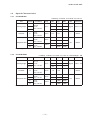
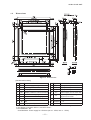
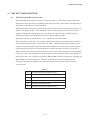
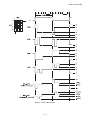
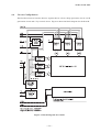
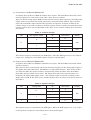
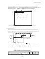
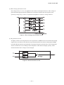
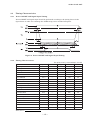
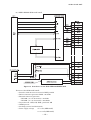
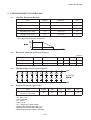
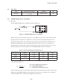
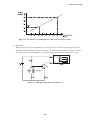
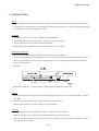
AN.No.G191D-460E LIQUID CRYSTAL DISPLAY MODULE G 1 9 1 D USER’S MANUAL Seiko Instruments Inc. AN.No.G191D-460E NOTICE This manual describes the technical information, as well as the functions and operation of the G191D Liquid Crystal Display Module made by Seiko Instruments Inc. Please read this manual carefully to familiarize yourself with the functions so you can make the best use of them. The descriptions here are subject to change without notice. Revision Record Edition Revision Date 1 Original June 1994 Seiko Instruments Inc. 1994 Printed in Japan i AN.No.G191D-460E CONTENTS G191D00P000, G191DB1P000 1. SPECIFICATIONS 1.1 General ................................................................................................................. 1 1.2 Features ............................................................................................................... 1 1.3 Absolute Maximum Ratings (excluding LED backlight) .................................... 2 1.4 Mechanical Characteristics ................................................................................. 2 1.5 Electrical Characteristics (excluding LED backlignt) ........................................ 2 1.6 Optical Characteristics ........................................................................................ 3 1.7 LCD Panel Life Time ........................................................................................... 4 1.8 Dimensions .......................................................................................................... 5 2. CIRCUIT CONFIGURATION 2.1 Liquid Crystal Driving Circuit ............................................................................ 6 2.2 Circuit Configuration .......................................................................................... 8 2.3 Timing Characteristics ...................................................................................... 12 2.4 Interface Circuit ................................................................................................ 14 G191DB1P000 3. LED BACKLIGHT 3.1 Absolute Maximum Ratings .............................................................................. 18 3.2 Electrical and Optical Characteristics .............................................................. 18 3.3 LED Backlight Connection Diagram ................................................................ 18 3.4 Brightness (panel upper side) ........................................................................... 18 3.5 Life Time ............................................................................................................ 19 3.6 LED Backlight Driver Examples ...................................................................... 19 4. PRECAUTIONS ........................................................................................................ 21 INDEX ii AN.No.G191D-460E 1. SPECIFICATIONS 1.1 General The G191D is a very thin LCD module on which a full-dot matrix LCD panel and a CMOS IC driver are integrated. The LCD panel used here features wide viewing angle and high contrast. This full dot configuration allows a wide variety of patterns to be displayed depending upon the input data. The display position is the intersection point of the matrix transparent electrodes. This prevents display distortion and displacement. 1.2 Features G191D00P000/G191DB1P000 192 × 192 full dot matrix configuration 1/192 duty, 1/12 bias Four-bit parallel data input A wide temperature range, gray mode STN LCD panel Positive display Display data H : Display ON : blue display color Display data L : Display OFF : gray background G191D00P000 Two types of power supply : VDD = +5V, VLC = -24V (for driving liquid crystal) Reflective type Weight : Approx. 62g G191DB1P000 Three types of power supply : VDD = +5V, VLC = -24V, LEDA (for driving LED) Transflective type A built-in LED backlight (color : yellow-green) Weight : Approx. 80g 1 AN.No.G191D-460E 1.3 Absolute Maximum Ratings (excluding LED backlight) Item Symbol Power supply voltage Max. Unit VDD 0 7.0 V VLC VDD-30.0 VDD V VDD-30.0 VDD V -0.3 VDD+0.3 V -20 +70 °C -30 +80 °C ≤ 48 hrs +20 +85 %RH ≤ 1000 hrs +20 +65 %RH Input voltage VIN Operating temperature Topr Storage temperature Tstg Storage humidity 1.4 VO≥VLC ≤65%RH Mechanical Characteristics Item Standard 192×192 dots Dot configuration Module dimensions (H × V × T) [mm] G191D00P000 : 86.0×95.0×7.0 G191DB1P000 : 86.0×95.0×9.0 Viewing area (H × V) [mm] 67.4×67.4 Active display area (H × V) [mm] 63.33×63.33 Dot dimensions (H × V) [mm] 0.3×0.3 Dot pitch (H × V) [mm] 0.33×0.33 Weight [g] G191D00P000 : 75 max. G191DB1P000 : 100 max. H : Horizontal 1.5 VSS=0V Min. VO Conditions V : Vertical T : Thickness (max.) Electrical Characteristics (excluding LED backlignt) VDD=5V±5%, VSS=0V, Ta=-20°C to +70°C Item Symbol Conditions VDD Power supply voltage VLC VO VDD=5V VO≥VLC Min Typ. Max. Unit 4.75 5.00 5.25 V -24.5 -24.0 -23.5 V -23.0 -5.0 V High VIH 0.8VDD VDD V Low VIL 0 0.2VDD V 5.0 10.0 mA 4.5 9.0 mA 65 70 75 Hz Input voltage IDD Current consumption*1 ILC Frame frequency VDD=5V, Ta=25°C VO=-18.9V fFLM=70Hz fFLM *1 Display patterns : checkered patterns. Display data shift clock frequency : fCL2=3.0MHz 2 AN.No.G191D-460E 1.6 Optical Characteristics 1.6.1 G191D00P000 1/192 duty, 1/12 bias, fFLM=70Hz, Vopr=VDD-VO Item Symbol θ1 Viewing angle θ2 θ2-θ1 Contrast C ton toff Response time Conditions Temp. C≥2.0 ∅=0° Vopr =23.9V 25°C θ=0° ∅=0° Vopr =23.9V 25°C θ=0° ∅=0° Vopr =23.9V 25°C θ=0° -20°C ∅=0° toff Vopr =26.0V Measuring instrument : Canon illuminometer LC-3S ton 1.6.2 G191DB1P000 Item Symbol θ2 θ2-θ1 Contrast Typ. Max. -5 35 40 2.5 3.0 200 320 130 210 1800 2900 1000 1600 Unit Reference Degree Notes 1 & 2 Note 3 ms Note 4 1/192duty, 1/12bias, fFLM=70Hz, Vopr=VDD-VO, LED backlight : ON θ1 Viewing angle Min. C ton toff Response time Conditions Temp. C≥1.4 ∅=0° Vopr =23.9V 25°C θ=0° ∅=0° Vopr =23.9V 25°C θ=0° ∅=0° Vopr =23.9V 25°C θ=0° -20°C ∅=0° toff Vopr =26.0V Measuring instrument : Canon illuminometer LC-3S ton 3 Min. Typ. Max. -15 30 45 1.5 2.0 200 320 130 210 1800 2900 1000 1600 Unit Reference Degree Notes 1 & 2 Note 3 ms Note 4 AN.No.G191D-460E Note 1 : Definition of angles θ and ∅ θ ′ ∅ Note 2 : Definition of viewing angles θ1 and θ2 ° θ θ ° θ ′ ∅ ° θ ∅ ′ ∅ θ ° ° θ θ Note 3 : Definition of contrast (C) Note 4 : Definition of response time Figure 1 Definition 1.7 LCD Panel Life Time Item Conditions Standard Unit Life time* 25°C±10°C <65%RH 100, 000 or more hrs * Definition of life time : the time up to occurrence of any of the following: · Contrast reduces to 30% of the initial value. · Current consumption becomes three times the initial value. · Orientation deteriorates significantly. · The display malfunctions. 4 AN.No.G191D-460E 1.8 Dimensions ± ± ± ± ± ± ± × ± ± ± Figure 2 Dimensions [I/O terminal functions] No. Symbol Functions No. Symbol Functions 1 VDD Power supply for logic : +5V 10 D1 Display data input 2 FGND Frame ground*1 11 D2 Display data input 3 CL2 Display data shift clock 12 D3 Display data input 4 INH Display ON/OFF control terminal*2 13 VLC Power supply for LC drive:-24V 5 FLM One-frame timing signal 6 CL1 One-common-line timing signal 14 VO Liquid crystal drive voltage adjustment terminal 7 VSS GND : 0V 15 VSS GND : 0V 8 M NC 16 NC/LEDA * 3 9 D0 Display data input 17 NC/LEDC *3 *1 The FGND terminal is connected to the module metal frame. Use this terminal to ground the frame. *2 The display is ON when INH is H, and OFF when L. *3 G191D00P000 : NC G191DB1P000 : Power supply for LED drive (NO.16 : LEDA, NO.17 : LEDC) 5 AN.No.G191D-460E 2. CIRCUIT CONFIGURATION 2.1 Liquid Crystal Driving Circuit The G191D LCD panel drive waveform is shown in Figure 3. Since DC voltage will damage the liquid crystal, AC voltage is applied between the two frames. The signal controlling this is the liquid crystal AC drive control signal M. Depending on the LCD panels, increasing the liquid crystal AC drive waveform frequency may improve the display quality. The G191D contains a circuit that generates AC drive control signal M, which has a higher frequency than that of M. The frequency of the M signal is adjusted according to the LCD panel to provide the best display quality. The frame frequency is normally set to 70 ± 5 Hz to prevent screen flicker. The G191D has a 1/192 duty cycle, and the common electrodes are selected within a frame by time division from electrode 1 to electrode 192. This is called line sequential scanning. The voltage level of the segment electrodes determines whether or not the dots at the intersection of the segment electrodes are selected when the common electrode is selected. As shown in Table 1, there are six drive waveform voltage levels, V a to Vf. The voltage level is determined by the bias value. The voltage between the segment and common electrode is then applied to the liquid crystal. The selection waveform for SEG0-COM0 and the non-selection waveform for SEG1-COM1 are shown in Figure 3. The size of the effective voltage of the waveform determines whether the liquid crystal under the selected dots is in the selection or nonselection state. Table 1 Va Common and segment selection level Vb Common non-selection level Vc Segment non-selection level Vd Segment non-selection level Ve Common non-selection level Vf Common and segment selection level 6 AN.No.G191D-460E Figure 3 Drive Waveform 7 AN.No.G191D-460E 2.2 Circuit Configulation The G191D consists of common drivers, segment divers, a bias voltage generation circuit, an M generation circuit and a Vopr control circuit. Figure 4 shows the block diagram for the G191D. ′ ′ × Figure 4 Block Diagram for G191D 8 AN.No.G191D-460E (1) Common driver (HITACHI HD66205TF) A common driver (CD) is a CMOS IC with 80 drive outputs. The G191D has three CDs, whose internal registers are connected to each other. They operate as follows. Input one-frame timing signal (FLM) is taken into the internal shift register by the falling edge trigger of the one-common-line timing signal (CL1), and sequentially shifted. After 192-CL1 input, the next FLM is input and the same operation is repeated. As shown in Table 2, the common output is selected according to the shift register contents and the internally-generated liquid crystal AC drive control signal (M) in the drive circuit, and the common drive waveform are formed. Table 2 Common Output INH Shift register content M' COM output H Va L Vf H Ve L Vb × Va Display H ON H L L × OFF × : Invalid The common output is controlled by the INH signal ; when the INH signal is low, the common output is Va, irrespective of the shift register contents or the M signal. (2) Segment driver (HITACHI HD66204TF) A segment driver (SD) is a CMOS IC with 80 drive outputs. The G191D has three SDs, which operate as follows. Input four-bit data is sequentially taken into the internal register by the falling edge trigger of the display data shift clock (CL2). The SDs have a chip enable function. After 80 bits of data are taken into SD1, the next bit of data is automatically taken into SD2. Since G191D has three SDs, 192 bits of data can be taken. The display data taken into internal register are latched by the falling edge trigger of CL1. The segment output is selected according to this display data and M in the drive circuit, and the segment drive waveform is formed as shown in the Table 3. Table 3 Segment Output INH Display data M' SEG output H Vf L Va H Vd L Vc × Va Display H ON H L L × OFF × : Invalid The segment output is controlled by the INH signal. When the INH signal is low, Va is output to the segment, irrespective of the display data and of the M signal. 9 AN.No.G191D-460E Therefore, by bringing the INH signal to low, Va is output both to the common and to the segment electrodes, making the voltage applied to the liquid crystal zero, and the display goes off. The relationship between the display data and display screen is shown below. Figure 5 Relationship between the Display Data and Display Screen (3) Vopr control circuit Display screen contrast and viewing angle are affected by changes in the liquid crystal operating voltage (Vopr). As shown in Figure 6, external VLC is supplied to the operational amplifier and Vopr (Va to Vf) is generated and applied to the LCD panel. Ω Ω Ω Figure 6 Vopr Control Circuit Also, display screen contrast and viewing angle are influenced by the ambient temperature. The recommended Vopr level at different temperatures is as follows. Table 4 Liquid Crystal Operating Voltage Temperature (°C) -20 0 25 50 70 Liquid crystal operating voltage(Vopr)* (V) 26.0 25.0 24.0 22.5 21.0 *Vopr ≈VDD-VO 10 AN.No.G191D-460E (4) Bias voltage generation circuit Six voltage levels, Va to Vf, are applied to the common and segment drivers. The voltage is generated through operational amplifiers by resistance division from the liquid crystal operating voltage (Vopr). Here, an operational amplifier is used as a voltage follower. Figure 7 Bias Voltage Generation Circuit (5) M generation circuit As Figure 8 shows, the M generation circuit performs an XOR on the one-common-line timing signal (CL1) (on which A time division is performed) and the one-frame timing signal (FLM) (on which B time division is performed), and outputs liquid crystal AC drive control signal M. Values A and B are set according to the LCD panel so that the best display quality can be obtained and the drive voltage can be changed. ′ Figure 8 M Generation Circuit 11 AN.No.G191D-460E 2.3 Timing Characteristics 2.3.1 Power ON/OFF and Signal Input Timing Power ON/OFF and signal input should be performed according to the timing shown in the figure below in order not to damage the LCD driving circuit and the LCD panel. + + + ≥ ≥ ≥ Figure 9 Power ON/OFF and Signal Input Timing 2.3.2 Timing Characteristics Item Symbol Ta=-20°C to 70°C, VDD=5.0V±5%, VSS=0V Min. Typ. Max. Unit FLM cycle time tCFLM 13.3 14.3 15.4 ms CL1 cycle time tCCL1 10 74.4 µs CL1 high level width tWCL1H 50 ns CL1 low level width tWCL1L 1 µs CL1 rise time tRCL1 30 CL1 fall time tFCL1 30 ns FLM setup time tFLMS 100 ns FLM hold time tFLMH 100 ns tDM ns tCCL2 125 300 ns CL2 high level width tWCL2H 45 ns CL2 low level width tWCL2L 45 ns CL2 rise time tRCL2 50* ns CL2 fall tim tFCL2 Allowable M delay time CL2 cycle time ns 50* ns tDS 20 Data setup time ns Data hold time tDH 20 ns CL2 rise to CL1 rise tLD ns CL2 fall to CL1 fall tSL 80 ns CL1 rise to CL2 rise tLS ns CL1 fall to CL2 fall tLH 80 ns *tRCL2, tFCL2 < tCCL2 - tWCL2H - tWCL2L 2 12 AN.No.G191D-460E Timing Chart 1 : Timing of Signal Input Into Common Driver Figure 10 Timing Chart 2 : Timing of Signal Input Into Segment Driver Figure 11 13 AN.No.G191D-460E 2.4 Interface Circuit 2.4.1 Interface with MPU signal The G191D is controlled by the MPU circuit, whose interface is easily set up when the LCD controller is used. The LCD controller has basic functions such as receiving information related to the display from the MPU circuit, sending display timing signals and display data to the LCD module, as well as other functions such as cursor display. The G191D must use an LCD controllers conforming to the following : For a full dot-matrix LCD module Where data is transferred to the LCD module in four-bit parallel Where G191D display screen has 1/192 duty The following section gives examples of interfaces using the Oki MSM6255GSK, Seiko Epson SED1330F/1335F, and Hitachi HD64646FS controllers. 14 AN.No.G191D-460E (1) OKI MSM6255GSK Ω Ω Ω Figure 12 Interface Circuit With MSM6255GSK Features of the MSM6255GSK : Interface with 80-series MPU possible Cursor ON/OFF Blinking speed, form, and position are programmable Scrolling and paging CMOS process Power supply voltage 5V±10% 15 AN.No.G191D-460E (2) SEIKO EPSON SED1330F/1335F Ω Ω Ω Figure 13 Interface Circuit With SED1330F/SED1335F Features of the SED1330F/1335F : Interface with 80-series or 68-series MPU possible Built-in character generator ROM : 160 kinds External character generator CG RAM : (8 × 16 dot matrix) × 64 kinds CG ROM : (8 × 16 dot matrix) × 256 kinds Layered mode : AND, OR, XOR, preferred OR CMOS process Scrolling (vertical and horizontal) Power supply voltage 5V ± 10% (SED1330F) 2.7 to 5.5V (SED1335F) 16 AN.No.G191D-460E (3) HITACHI HD64646FS Ω Ω Ω Figure 14 Interface Circuit With HD64646FS Features of the HD64646FS : Interface with 80-series MPU possible Layered mode : OR (character and graphics) Character reverse, blinking, all black, all white Cursor ON/OFF Blinking speed, form and position are programmable 17 Character font Vertical : 1 to 32 dots Horizontal : 8 dots Scrolling Vertical : smooth or character unit Horizontal : character unit CMOS process Power supply voltage 5V ± 10% AN.No.G191D-460E 3. LED BACKLIGHT (G191DB1P000) 3.1 Absolute Maximum Ratings Item Symbol Standard Unit DC forward current IF 200* mA DC reverse voltage VR 8 V Allowable dissipation PD 950 mW Operating temp. range Topr -20 to +70 °C Storage temp. range Tstg -30 to +80 °C * Forward current reduction characteristics : The absolute maximum rating of the forward current varies depending on ambient temperature. ° 3.2 Electrical and Optical Characteristics Ta=25°C Item Symbol Meas. Condition Min. Typ. Max. Unit Forward voltage VF IF=100mA 3.7 4.1 4.5 V Reverse current IR VR=8V 0.3 mA 3.3 LED Backlight Connection Diagram 3.4 Brightness (panel upper side) Item Symbol Min. Typ. Max. Unit Surface brightness (Center of LCD panel) BP 1.0 2.0 nit Measurement conditions and a measuring instrument are : Ta = 25°C ± 3°C 30% to 85%RH IF = 100mA fFRM = 70Hz VLC = Optimum LC drive voltage Display OFF (Entire display data = “L”) Measured 30 minutes after LED lights Measuring instrument : BM-7 (TOPCON) 18 AN.No.G191D-460E 3.5 Life Time Item Measurement conditions Standard Unit Ta=25°C±10°C 50,000 or more hrs IF =100mA *Definition of life time : The time until the brightness decreases to half of the initial brightness. Life time* 3.6 LED Backlight Driver Examples (1) Example 1 A basic LED backlight driver example is shown in Figure 15. Ω Figure 15 LED Backlight Driver Example 1 Where resistance R is the limit resistance of the LED forward current. The forward current depends upon the temperature. Especially, it must be decreased at high temperature. For temperature dependence, refer to forward current reduction characteristics described in 3.1. The operating temperature for the G191D ranges from -20°C to +70°C. It is necessary to determine limit resistance R so that the forward current becomes 50 mA or lower at +70°C. Forward voltage VF at each temperature of the LED backlight is shown in Table 5. Table 5 Forward Voltage At Temperatures Temperature (Ta) Conditions VF min. VF typ. VF max. -20°C IF=100mA 3.9V 4.3V 4.7V +25°C IF=100mA 3.7V 4.1V 4.5V +70°C IF=50mA 3.4V 3.6V 3.9V Limit resistance R is calculated using the following equation. The resistance becomes the value shown in Figure 15. VIN - VF R= (Ω) IF VIN = Input voltage (power voltage) (V) VF = LED forward voltage (V) IF = Allowable LED forward current (A) For this resistance value, the forward current becomes lower than 50 mA at 25°C. The surface brightness of the LED backlight varies with the forward current. See Figure 16. Compared with 3.4 brightness (IF = 100 mA), the brightness is about 30%. 19 AN.No.G191D-460E Figure 16 Forward Current-Brightness Characteristics (Ta = 25°C) (2) Example 2 When you want to keep the brightness (2 nit) at 25°C, use a thermosensitive element, like a thermistor, and a transistor as shown in Figure 17. Set the thermosensitive element to about IF = 100 mA at 25°C and configure it so that IF will be reduced as the temperature rises. Figure 17 LED Backlight Driver Examples 2 20 AN.No.G191D-460E 4. PRECAUTIONS Safety If the LCD panel breaks, be careful not to get the liquid crystal material in your mouth and not to be injured by crushed glasses. If the liquid crystal material touches your skin or clothes, wash it off immediately using soap and plenty of water. Handling Avoid static electricity, as this can damage the CMOS LSI. The LCD panel is made of plate glass ; do not hit or press against it. Do not remove the panel or frame from the module. The polarizer on the display is very fragile; handle it very carefully. Mounting and Design Mount the module using the specified installation sections and holes. To protect the module from external pressure, put a plate of transparent material such as acrylic or glass over the display surface, frame, and polarizer. Leave a small gap between the transparent plate and the module. YExample Keep the module dry. Condensation can damage the transparent electrodes. Storage Store the module in a dark place where the temperature is 25°C ± 10°C and the humidity is below 65% RH. Do not store the module near organic solvents or corrosive gases. Do not crush, shake, or jar the module or its components. Cleaning Do not wipe the polarizer with a dry cloth, as it may scratch the surface. Wipe the module gently with a soft cloth soaked with a petroleum benzine. Do not use ketonic solvents (ketone and acetone) or aromatic solvents (toluene and xylene), as they may damage the polarizer. 21 AN.No.G191D-460E Index A Allowable dissipation .................................................................................................... 18 B Bias value ....................................................................................................................... 6 Bias voltage generation circuit ................................................................................ 8, 11 Block diagram ................................................................................................................. 8 Brightness .......................................................................................................... 18, 19, 20 C Chip enable function ...................................................................................................... 9 Cleaning ........................................................................................................................ 21 Common drive waveform ............................................................................................... 9 Common driver ...................................................................................................... 8, 9, 13 Contrast ...................................................................................................................... 3, 4 Current consumption ..................................................................................................... 2 D Definition of contrast ...................................................................................................... 4 Definition of response time ............................................................................................ 4 Definition of viewing angles ........................................................................................... 4 Display data input .......................................................................................................... 5 Display data shift clock .......................................................................................... 2, 5, 9 Display ON/OFF control terminal ................................................................................. 5 Drive waveform .......................................................................................................... 6, 7 E Effective voltage ............................................................................................................. 6 F Flicker ............................................................................................................................. 6 Forward current ..................................................................................................... 18, 19 Forward current reduction characteristics ............................................................ 18, 19 Forward voltage ...................................................................................................... 18, 19 Frame frequency ..................................................................................................... 2, 4, 6 Frame ground ................................................................................................................. 5 H HITACHI HD64646FS ........................................................................................... 14, 17 I Input voltage ............................................................................................................... 1, 2 Interface ........................................................................................................................ 14 I/O terminal functions .................................................................................................... 4 AN.No.G191D-460E L LCD controller .............................................................................................................. 14 Life time .................................................................................................................... 4, 19 Limit resistance ............................................................................................................ 19 Liquid crystal drive voltage adjustment terminal ........................................................ 5 Liquid crystal AC drive control signal .................................................................. 6, 9, 11 Liquid crystal operating voltage .................................................................................. 10 M M generation circuit ................................................................................................ 8, 11 N Non-selection waveform ............................................................................................. 5, 6 O OKI MSM6255GSK ................................................................................................ 14, 15 One-common-line timing signal ............................................................................ 5, 9, 11 One-frame timing signal ....................................................................................... 5, 9, 11 Operating temperature ............................................................................................ 2, 18 Operational amplifier ............................................................................................. 10, 11 P Positive display ............................................................................................................... 1 Power supply voltage ............................................................................. 15, 16, 17, 18, 20 R Resistance division ....................................................................................................... 11 Response time (fall) ........................................................................................................ 4 Response time (rise) ....................................................................................................... 4 Reverse current ...................................................................................................... 18, 19 Reverse voltage ....................................................................................................... 18, 19 S Segment drive waveform ................................................................................................ 9 Segment drive ........................................................................................................8, 9, 13 SEIKO EPSON SED1330F/1335F ......................................................................... 14, 16 Selection waveform .................................................................................................... 6, 7 Storage .......................................................................................................................... 21 Storage humidity ............................................................................................................ 2 Storage temperature ................................................................................................ 2, 18 T Timing characteristics .................................................................................................. 12 V Viewing angle ................................................................................................................. 3 Vopr control circuit ................................................................................................... 8, 10 Seiko Instruments Inc. Head Office Components Sales Division 1-8, Nakase, Mihama-Ku. Chiba-shi, Chiba 261-8507. Japan Phone : 043-211-1216 FAX : 043-211-8032 Seiko Instruments U.S.A. Inc. Electronic Components Division 2990 W. Lomita Blvd., Torrance Calif. 90505, USA Phone : 310-517-7770 FAX : 310-517-8131 Seiko Instruments GmbH Siemensstrasse 9b, 63263 Neu-Isenburg, Germany Phone : 49-6102-297-122 FAX : 49-6102-297-116 Seiko Instruments (H.K.) Ltd. Sales Division 4-5/F, Wyler Centre 2, 200 Tai Lin Pai Road, Kwai Chung, N. T., Kowloon, Hong Kong Phone : 852-24218611 FAX : 852-24805479 Seiko Instruments Taiwan Inc. 4FL, No.40, Sec.2, Min Chuan E., Taipei, Taiwan, R.O.C. Phone : 886-2-563-5001 FAX : 886-2-521-9519 Seiko Instruments Singapore Pte. Ltd 2, Marsiling Lane Singapore 739144 Phone : 65-2691370 FAX : 65-2699729


![取扱説明書[総合 デジタル]](http://vs1.manualzilla.com/store/data/006685889_2-1b0f2c4846877645fa42fa549f2a320c-150x150.png)