1
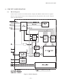
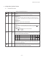
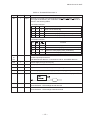
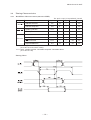
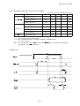
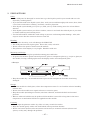
AN.No.G121C-C-561E LIQUID CRYSTAL DISPLAY MODULE G121C00P00C G121CB1P00C USER’S MANUAL Seiko Instruments Inc. AN.No.G121C-C-561E NOTICE This manual provides technical information covering functions and operational instructions for the G121C liquid crystal display modules with a built-in LCD controller. Please read through this manual before operating the product. Distribution of this manual to third parties for any purpose other than operation of the product is prohibited. The descriptions herein are subject to change without prior notice. Application information is intended solely for general guidance. Use of the information contained herein for the users application is done at the users risk. Revision Record Version Revision Date 1 Original September 1994 2 June 1995 Copyright 1994 by Seiko Instruments Inc. Printed in Japan i AN.No.G121C-C-561E CONTENTS G121C00P00C, G121CB1P00C 1. SPECIFICATIONS 1.1 General ................................................................................................................. 1 1.2 Features ............................................................................................................... 1 1.3 Absolute Maximum Ratings (excluding LED backlight) .................................... 2 1.4 Mechanical Characteristics ................................................................................. 2 1.5 Electrical Characteristics (excluding LED backlight) ........................................ 3 1.6 Optical Characteristics ........................................................................................ 4 1.7 LCD Panel Lifetime ............................................................................................. 6 1.8 Dimensions .......................................................................................................... 7 2. CIRCUIT CONFIGURATION 2.1 Block Diagram ..................................................................................................... 8 2.2 LCD Controller (SEIKO EPSON SED1335F) .................................................... 9 2.3 Common Driver (HITACHI HD66205TF) .......................................................... 9 2.4 Segment Drivers (HITACHI HD66204TF) ......................................................... 9 2.5 Vopr Control Circuit .......................................................................................... 10 2.6 Bias Voltage Generator ..................................................................................... 11 2.7 M Generator ...................................................................................................... 11 3. OPERATING INSTRUCTIONS 3.1 Terminal Functions ........................................................................................... 12 3.2 Timing Characteristics ...................................................................................... 14 3.3 Reset ................................................................................................................... 16 3.4 Setting the Power Supply and the Signals to On or Off .................................. 16 3.5 Commands ......................................................................................................... 17 3.6 Display Data RAM ............................................................................................. 18 3.7 Example of an Initial Setting ............................................................................ 18 3.8 Example of MPU Interface ................................................................................ 23 G121CB1P00C 4. LED BACKLIGHT 4.1 Absolute Maximum Ratings .............................................................................. 24 4.2 Electro-optical Characteristics .......................................................................... 24 4.3 LED Backlight Diagram .................................................................................... 24 4.4 Brightness (Top surface of LCD) ....................................................................... 24 4.5 Lifetime .............................................................................................................. 25 4.6 Examples of LED Backlight Drivers ................................................................. 25 G121C00P00C, G121CB1P00C 5. PRECAUTIONS ........................................................................................................ 27 INDEX ii AN.No.G121C-C-561E 1. SPECIFICATIONS 1.1 General The G121C is a very thin LCD module which incorporates a full-dot matrix LCD panel and CMOS IC driver. G121C can be used within a wide temperature range. The built-in LCD controller (SED1335F) also interfaces easily with an MPU. This full-dot configuration allows a wide variety of patterns to be displayed depending upon the input data. There is no distortion or displacement in the display because the display position is the point on the matrix where the transparent electrodes intersect. 1.2 Features G121C00P00C/G121CB1P00C : 128 × 128 full dot matrix configuration 1/128 duty, 1/10 bias Built-in LCD controller SED1335F Selectable interface between an 80 series MPU and a 68 series MPU 8KB internal display data RAM Built-in 160 character (5 × 7 dots) CGROM STN LCD with a wide operating temperature range and gray mode Positive display Display data H : Display ON : blue display color Display data L : Display OFF : gray background color G121C00P00C : Dual power supplies : VDD = +5V, VLC = -24V (LCD driving voltage) Reflective Weight : Approximately 64g G121CB1P00C : Triple power supplies : VDD = +5V, VLC = -24V (LCD driving voltage), LEDA (LED anode) Transflective Built-in LED backlight (color : yellow-green) Weight : Approximately 81g 1 AN.No.G121C-C-561E 1.3 Absolute Maximum Ratings (excluding LED backlight) Item Symbol Power supply voltage Min. Max. Unit VDD -0.3 7.0 V VLC VDD-30.0 VDD V VDD-30.0 VDD V -0.3 VDD+0.3 V -20 +70 °C -30 +80 °C ≤ 48 hrs 20 85 %RH ≤ 1000 hrs 20 65 %RH VO Input voltage VIN Operating temperature Topr Storage temperature Tstg Storage humidity 1.4 Conditions VSS=0V VO ≥ VLC ≤ 65%RH Mechanical Characteristics Item Standard 128×128 dot Dot configuration Module dimensions (H × V × T) [mm] G121C00P00C : 86.0×95.0×8.0 max. G121CB1P00C : 86.0×95.0×10.0 max. Viewing area (H × V) [mm] 67.4×67.4 Active display area (H × V) [mm] 62.69×62.69 Dot dimensions (H × V) [mm] 0.46×0.46 Dot pitch (H × V) [mm] 0.49×0.49 Weight [g] G121C00P00C : 75 max. G121CB1P00C : 100 max. H : Horizontal V : Vertical T : Thickness (max.) 2 AN.No.G121C-C-561E 1.5 Electrical Characteristics (excluding LED backlight) Item Symbol Conditions VDD Power supply voltage VLC VO 4.75 5.00 5.25 V -24.5 -24.0 -23.5 V -23.0 -5.0 V Input (CMOS) High VIHC 0.8VDD VDD V Low VILC 0 0.2VDD V Input voltage2 (TTL) High VIHT 0.5VDD VDD V Low VILT 0 0.2VDD V Input voltage3 (RES) High VT+ 0.5VDD 0.7VDD 0.8VDD V Low VT- 0.2VDD 0.3VDD 0.5VDD V High VOH IOH=-5.0mA 2.4 V Low VOL IOL=5.0mA VDD=5V, Ta=25°C VO=-15.0V fFLM=71.4Hz 0.4 V 10.0 15.0 mA 4.1 6.2 mA 71.4 Hz voltage1 Output voltage4 Current consumption5 Frame frequency 1 2 3 4 5 VDD=5V VO≥VLC VDD=5V±5%, VSS=0V, Ta=-20°C to +70°C Min Typ. Max. Unit IDD ILC fFLM Applied to SEL1 and SEL2. Applied to INH, A0, CS, RD, WR, and D0 to D7. Applied to RES. Applied to D0 to D7. Display patterns : Checkered patterns, Display data shift clock frequency : fCL2 = 6.0MHz 3 AN.No.G121C-C-561E 1.6 Optical Characteristics 1.6.1 G121C00P00C 1/128 duty, 1/10 bias, fFLM=71.4Hz, Vopr=VDD-VO Item Sym. θ1 Viewing angle θ2 θ2-θ1 Contrast C ton toff ton Response time toff ton toff Conditions Temp. C≥2.0 ∅=0° Vopr =20.0V 25°C θ=0° ∅=0° Vopr =20.0V 25°C θ=0° ∅=0° Vopr =20.0V 25°C θ=0° ∅=0° Vopr =21.5V -10°C θ=0° ∅=0° Vopr =22.0V -20°C Min. Typ. Max. -5 50 55 2.5 3.5 150 240 110 180 1060 1700 500 800 2860 4600 780 1300 Unit Remark Degree Refer to Notes 1 and 2 Note 3 ms Note 4 Measuring instrument : Canon illuminometer LC-3S 1.6.2 G121CB1P00C Item 1/128 duty, 1/10 bias, fFLM=71.4Hz, Vopr=VDD-VO, backlight : ON Sym. θ1 Viewing angle θ2 θ2-θ1 Contrast C ton toff ton Response time toff ton toff Conditions Temp. C≥1.4 ∅=0° Vopr =20.0V 25°C θ=0° ∅=0° Vopr =20.0V 25°C θ=0° ∅=0° Vopr =20.0V 25°C θ=0° ∅=0° Vopr =21.5V -10°C θ=0° ∅=0° Vopr =22.0V -20°C Min. Typ. Max. -20 30 50 2.0 2.4 150 240 110 180 1060 1700 500 800 2860 4600 780 1300 Unit Remark Degree Refer to Notes 1 and 2 Note 3 ms Note 4 Measuring instrument : Canon illuminometer LC-3S 4 AN.No.G121C-C-561E Note 1 : Definition of angle θ and ∅ θ ′ ∅ Note 2 : Definition of viewing angles θ1 and θ2 ° θ θ ° θ ′ ∅ ° θ ∅ ′ ∅ θ ° ° θ θ Note 3 : Definition of contrast (C) Note 4 : Definition of response time Figure 1 Definition 5 AN.No.G121C-C-561E 1.7 LCD Panel Lifetime Item Conditions Standard Unit Lifetime* 25°C±10°C <65%RH 100,000 or more hrs * Definition of lifetime : the time up to occurrence of any of the following : ·Contrast reduces to 30% of the initial value. ·Current consumption becomes three times the initial value. ·Orientation deteriorates significantly. ·The display malfunctions. 6 AN.No.G121C-C-561E 1.8 Dimensions ± ± ± ± ± ± ± ± × ± ± Figure 2 Dimensions I/O terminal functions No. Sym. Functions 1 RES Reset signal input 80 series MPU ⋅⋅⋅ Read signal 2 RD 68 series MPU ⋅⋅⋅ "E" clock 80 series MP ⋅⋅⋅ Write signal 3 WR 68 series MP ⋅⋅⋅ R/W signal 80/68series MPU bus switching 4 S E L2 terminal 80/68series MPU bus switching 5 S E L1 terminal 6 CS Chip select input Identifying signal for data bus 7 A0 signal 8 D0 Data bus line 9 D1 Data bus line 10 D2 Data bus line No. 11 12 13 14 15 Sym. D3 D4 D5 D6 D7 Data Data Data Data Data 16 VDD Power supply for logic circuit (+5V) 17 V SS 18 VO 19 V LC GND (0V) Adjustment terminal for liquid crystal driving voltage Power supply terminal for driving liquid crystal display (-24V) Display on/off control terminal 20 INH1 21 NC/LEDA 22 NC/LEDC Functions bus bus bus bus bus line line line line line 2 2 1 After powering on, DC voltage is not applied to LCD by setting INH "L" until the initialization of LCD controller is completed. After DISP ON command is executed, the display is set to on by setting INH "H" and set to off by setting INH "L". 2 G121C00P00C : NC G121CB1P00C : Power supply for LED backlight (No.21 : LEDA, No.22 : LEDC) 7 AN.No.G121C-C-561E 2. CIRCUIT CONFIGURATION 2.1 Block Diagram G121C**P**C consists of an LCD controller, display data RAM, common drivers, segment drivers, a Vopr control circuit, a bias voltage generator, M generator and so forth. Figure 3 shows the block diagram. ′ ′ × Figure 3 Block Diagram 8 AN.No.G121C-C-561E 2.2 LCD Controller (SEIKO EPSON SED1335F) The LCD controller (SED1335F) is located between the MPU and the LCD panel. The LCD controller stores the character codes and the bit-mapped graphics data from the MPU in the display data RAM (8KB), and then periodically reads out the stored data, converts it, and sends the converted signal to the LCD module. Also, through many command functions, it is possible to overlap the character screen with the graphics screen and scroll the screen in all directions. 2.3 Common Driver (HITACHI HD66205TF) The common driver (CD) is an 80 drive output CMOS IC. Two CDs are used in conjunction with each other in the G121C and operate as follows : The CDs read the input one-frame timing signal (FLM) into the internal register at the onecommon line timing signal (CL1) fall edge trigger and shift it sequentially. The common drive waveform is formed by the contents of this shift register and the signal to make the liquid crystal drive waveform AC (M). There are six voltage levels (Va to Vf) in the waveform. Table 1 shows the description of each level. Note that FLM signal and CL1 signal are input from LCD controller. After CL1 is input 128 times, the next FLM is input and the same operation is repeated. Table 1 Description of each voltage level Va Common, segment selection level Vb Common non-selection level Vc Segment non-selection level Vd Segment non-selection level Ve Common non-selection level Vf Common, segment selection level INH signal and YDIS signal from the LCD controller control COM output. When INH signal or YDIS signal is set to L, Va is output to COM output regardless of the contents of the shift register and M signal. 2.4 Segment Driver (HITACHI HD66204TF) The segment driver is an 80 drive output CMOS IC. Two segment drivers are used in the G121C and operate as follows : 4 bit input display data is read sequentially into the internal register at the display data shift clock (CL2) fall edge trigger. This display data and CL2 signal are input from the LCD controller. Because a chip enable function is built into the segment driver, when the 80 bit 9 AN.No.G121C-C-561E display data is input to SD1, the next data is automatically sent to segment driver 2. The two segment drivers read 128 bit display data. Thus the input display data in the internal register is latched at the one-common line timing signal (CL1) fall edge trigger. The segment drive waveform is formed by the display data and the signal to make the liquid crystal drive waveform AC (M). The INH signal and the YDIS signal from the LCD controller control SEG output. When the INH signal or the YDIS signal is set to L, Va is output to SEG output regardless of the contents of the shift register and M signal. Consequently, when the INH at the input terminal or the YDIS signal from the LCD controller is set to L, Va is applied to COM output and SEG output, 0V is applied to the liquid crystal and the display is set to off. 2.5 Vopr control circuit The viewing angle of the LCD panel and the shade of the screen depends on the liquid crystal operating voltage (Vopr). With the G121C, VLC is applied from outside. This VLC, as shown in Figure 4, is supplied with an operational amplifier and the voltage Vopr (Va to Vf ) applied to the LCD panel is generated. Ω Ω Ω Figure 4 Vopr Control Circuit Also, the viewing angle of the LCD panel and shade of the screen depend on the ambient temperature. The recommended values of the Vopr for the ambient temperature are as follows : Table 2 LC operating voltage Temperature (°C) -20 0 25 50 70 Voltage(Vopr)* (V) 22.0 21.5 20.0 19.0 18.0 *Vopr ≈VDD-VO 10 AN.No.G121C-C-561E 2.6 Bias Voltage Generator Six levels of voltage Va to Vf are applied to the drivers as a bias voltage. This voltage is generated from Vopr by dividing the resistance and driven by a voltage follower through an operational amplifier. Figure 5 Bias Voltage Generator 2.7 M Generator M generator outputs the Ex-ORed signal between the divided signal of the one-common line timing signal (CL1) to A and the divided signal of the one-frame timing signal (FLM) to B as M, which makes up the LC drive waveform AC. The values of A and B are set according to the LC panel to allow for the best quality display and to allow the drive voltage to be converted to AC. ′ Figure 6 M generator 11 AN.No.G121C-C-561E 3. OPERATING INSTRUCTIONS 3.1 Terminal Functions Table 3 Terminal Functions 1 Signal Q’ty I/O Functions RES 1 Input Active “L” Executes initial reset to the LCD controller by hardware. RD 1 Input 80 series MPU Active “L” Strobe signal when MPU reads out the data or the status flag from the LCD controller. The data bus of LCD controller is set to the output status during “L” 68 series MPU Active “H” Enable clock input terminal of 68 series MPU WR 1 Input 80 series MPU Active “L” Strobe signal when 80 series MPU writes the data or the parameters into LCD controller. LCD controller fetches the data bus signal at the WR rise edge. 68 series MPU R/W control signal input terminal of 68 series MPU. R/W= “H” : READ R/W= “L” : WRITE SEL1 SEL2 1 1 Input Input MPU interface can be switched by the combination of SEL1 and SEL2, and can be connected directly to both 80 series MPU (Z80, 8085, etc.) data bus and 68 series MPU (6809, 6802) data bus. SEL1 SEL2 Interface A0 RD WR CS 0 0 80 series A0 RD WR CS 1 0 68 series A0 E R/W CS 0 1 * * * * * 1 1 * * * * * * : Prohibited Normally SEL1 and SEL2 are directly connected to either power supply VDD or VSS to prevent noise. CS 1 Input Active “L” Inputs the chip select signal normally acquired by decoding the address bus signal when the MPU accesses the LCD controller. 12 AN.No.G121C-C-561E Table 4 Terminal Functions 2 Signal Q’ty I/O A0 1 Input Functions Normally connected to the least significant bit of MPU address. The data bus signal is identified by the combination of RD and WR or R/W and E as shown in the following tables: <80 series interface> A0 RD WR functions 0 0 1 Reads out the status flag 1 0 1 Reads out the data (display data, cursor address) 0 1 0 Writes the data (display data, parameters) 1 1 0 Writes commands (only codes) <68 series interface> RD WR A0 functions (E) (R/W) 0 1 1 Reads out the status flag 1 1 1 Reads out the data (display data, cursor address) 0 1 0 Writes the data (display data, parameters) 1 1 0 Writes commands (only codes) D0 to D7 8 I/O Active “H” Tristate input/output terminal 8 bit bidirectional data bus. Connected to 8 bit or 16 bit MPU data bus. VDD 1 Power supply for logic circuit (+5V) VSS 1 GND (0V) V0 1 Adjustment terminal for liquid crystal driving voltage VLC 1 Power supply terminal for driving liquid crystal display (-24V) INH 1 Input LEDA 1 G121C00P00C : NC G121CB1P00C : LED backlight anode terminal LEDC 1 -G121C00P00C : NC G121CB1P00C : LED backlight cathode terminal When INH= “H’, the display is ON and when INH= “L’, the display is OFF. 13 AN.No.G121C-C-561E 3.2 Timing Characteristics 3.2.1 Read/Write Characteristics (80 series MPU) Signal Item Ta= -20°C~+70°C, VDD=5.0V±5%, VSS=0V Symbol Min. Typ. Max. Unit Address hold time tAH8 10 ns Address setup time tAW8 0 ns System cycle time tCYC8 * ns Control pulse width tCC 120 ns Data hold time tDH8 5 ns Data setup time tDS8 120 ns RD access time tACC8 50 ns Output disable time tOH8 10 50 ns A 0, C S WR, RD D0 to D7 *tCYC8 = 785 : Applies to "Memory control command" and "System control command." (tCYC8=2tC+tCC+tCEA+75>tACT+245) tCYC8 = 820 : Applies to all the commands except the commands above. (tCYC8=4tC+tCC+30) Timing Chart 14 AN.No.G121C-C-561E 3.2.2 Read/Write Characteristics (68 series MPU) Signal A0, CS, WR Item Ta= -20°C~+70°C, VDD=5.0V±5%, VSS=0V Symbol Min. Typ. Max. Unit Address hold time tAH6 0 ns Address setup time tAW6 0 ns System cycle time tCYC6 * ns Data hold time tDH6 0 ns Data setup time tDS6 100 ns Access time tACC6 85 ns Output disable time tOH6 10 50 ns Enable pulse width tRDW 120 ns D0 to D7 RD *tCYC6 = 785 : Applies to "Memory control command" and "System control command." (tCYC6=2tC+tRDW+tCEA+75>tACV+245) tCYC6 = 820 : Applies to all the commands except the commands above. (tCYC6=4tC+tCC+30) Note : tCYC6 indicates the cycle of RD(E) signal while CS·RD(E)="H." It doesn't unconditionally indicate the cycle of RD(E) signal. Timing Chart 15 AN.No.G121C-C-561E 3.3 Reset × × Figure 7 Reset Inputting reset pulse resets the internal status of the LCD controller after powering on. The width of the pulse input must be 1 msec or more. The control signal for the LCD is cut off when in the reset status. Consequently, the LCD is driven by DC and the display quality deteriorates. Therefore, set INH to L to reset in the status in which DC is not applied to LCD. The instructions from the CPU cannot be accepted during this period. After resetting, set the default values immediately in order to set the internal registers after resetting. 3.4 Setting the Power Supply and the Signals to On or OFF Set the power supply and the signals to on or off according to the following timing chart list to avoid malfunctions of the drive circuit and the LC panel. + + + + ≥ ≥ ≥ Figure 8 Timing of setting the power supply and the signals to on and off 16 AN.No.G121C-C-561E 3.5 Commands Table 5 Commands Purpose System Control Display Control Drawing Control Memory Control Command C ode HEX Description Parameters Remarks RD WR A0 D7 D6 D5 D4 D3 D2 D1 D0 SYSTEM SET 101 01000000 Setting the 40 initial operation and the window P1 to P8 SLEEP IN 101 01010011 53 Sleep Operation 0 DISP ON/OFF 101 0101100D 58 Display on/off, 59 flashing screen P1 SCROLL 101 01000100 Setting display 44 start address and the display area CSRFORM 101 01011101 5D Setting the shape of thecursor, etc. P 1, P 2 CGRAM ADR 101 01011100 5C Setting CG RAM start address P 1, P 2 CSDIR 101 HDOT SCR 101 01011010 OVLAY 101 01011011 5B Display overlaying mode CSRW 101 01000110 46 Setting cursor address P 1, P 2 Note 1 CSRR 101 01000111 47 Reading cursor address P 1, P 2 Note 1 MWRITE 101 01000010 42 Writing into display memory MREAD 101 01000011 43 Reading display memory data Note 1) CD CD 01001110 4C Setting the cursor to movement direction 4F Setting the scrolling 5A position per dot in the horizontal direction P1 to P10 Note 1 Note 1 Note 1 0 P1 P1 A command is executed every time each parameter is input to the LCD controller and completed when the following parameters (P) or command (C) is entered. Consequently, the MPU can abort sending the parameters and send the following command. In this case the parameters which have been sent are effective and the values of the remaining parameters which have not been sent remain unchanged. Note that 2 byte parameters are handled as follows : 1) CSRW and CSRR commands : Parameters are executed per byte. Consequently only the lower bytes can be changed or checked. 2) All the commands but CSRW and CSRR commands : Executed after the second byte of the parameter is entered. (SYSTEM SET, SCROLL, CGRAM ADR) * 2 byte parameter indicates 1 data with 2 bytes such as APL and APH. For a description of commands and their parameters, refer to “SED1335F/1336F LCD Controller IC Application Manual” (Seiko Epson Corporation). 17 AN.No.G121C-C-561E 3.6 Display Data RAM The built-in LCD controller can control 512 Kbit (0000H to FFFFH) of the VRAM area. However, because the G121C has only 64 Kbit of built-in VRAM, the upper 3 bits are not effective. Consequently, when you define the addresses over 2000H, the display data is destroyed because the data is mapped to the VRAM area defined by the lower 13 bits. Do not map the data onto addresses over 2000H. When you define 65 or more customized character fonts (max. 256 characters) on CGRAM and display them simultaneously, you must map them onto VRAM addresses F000H through FFFFH. Note that this corresponds to 1000H through 1FFFH in VRAM of the G121C. Because all the character codes are assigned to CGRAM, the built-in CGROM cannot be used together with CGRAM. Figure 9 Display Data RAM 3.7 Example of an Initial Setting 18 AN.No.G121C-C-561E In the combination of characters and graphics Requirements 128 × 128 dots : 1 screen driving method (1/128 duty) First layer : Character screen Second layer : Graphics screen Character font : 8 × 8 dots CG RAM unused fOSC = 6 MHz, Frame frequency = 71.2 Hz Assigning display memory First layer (Character screen) Characters in the horizontal direction = 128/8 = 16 Characters in the vertical direction = 128/8 = 16 Consequently, the required memory size is 16 × 16 = 256 bytes Second layer (Graphics screen) Characters in the horizontal direction = 128/8 = 16 Characters in the vertical direction= 128/1 = 128 Consequently, the required memory size is 16 × 128 = 2048 bytes [Display and memory] Figure 11 Display and memory 19 AN.No.G121C-C-561E No. Command Operation 1 POWER ON 2 WAIT FOR POWER SUPPLY TO BE STABILIZED Sets VDD ≥ 4.5V and waits more than 3 msec after completing external resetting. 3 SYSTEM SET C = 40H P1 = 30H Initializes LCD controller 4 M0 : Internal CG ROM M1 : No compensation in bit D6 (CG RAM 32 characters MAX.) M2 : Character font size in the Y direction (8 dots) W/S : 1 screen driving method IV : No compensation in the top line P2 = 87H FX : Character field in the X direction (8 dots) WF : 2-frame AC drive P3 = 07H FY : Character field in the Y direction (8 dots) P4 = 0FH C/R : Characters in the X direction (Number of addresses) (16 characters/line) P5 = 49H TC/R : Total characters in the X direction (Number of addresses) (73 characters/line) fOSC = 6 MHz, Frame frequency = 71.2Hz P6 = 7FH L/F : Display lines in the Y direction (128) P7 = 10H P8 = 00H AP : Addresses in the X direction of virtual screen (16 addresses) SCROLL C = 44H P1 = 00H P2 = 00H Sets the start address of the first block screen to 0000H. P3 = 7FH Sets the display lines of the first block screen to 128. P4 = 00H P5 = 01H Sets the start address of the second block screen to 0100H. P6 = 7FH Sets the display lines of the second block screen to 128. 20 AN.No.G121C-C-561E No. 5 6 7 8 Command Operation HDOT SCR C = 5AH P1 = 00H Sets the dot shift in the X direction to 0. OVLAY C = 5BH P1 = 00H MX1, MX0 : Simple overlay (OR) DM1 : First block screen (Character mode) DM2 : Third block screen (Character mode) OV : Combination of character mode and graphics mode DISP ON/OFF C = 58H P1 = 16H D : All screen display OFF FC1, FC0 : Blinking with cursor ON (Approx. 2 Hz) FP1, FP0 : First block screen display ON FP3, FP2 : Second block screen display ON FP5, FP4 : Third block screen display OFF CLEAR FIRST LAYER DISPLAY DATA Writes space character code 20H onto the corresponding first layer memory (character screen). CSRW C = 46H P1 = 00H P2 = 00H Sets the VRAM address corresponding to the start address of the first block screen (home address). CSR DIR C = 4CH Sets “+1” to the automatic shift direction of the address counter. MWRITE C = 42H P1 = 20H P2 = 20H ⋅ ⋅ ⋅ Pn = 20H, Sets the space code. Sets the space code. ⋅ ⋅ ⋅ Sets the space code. (n = 256) 21 AN.No.G121C-C-561E No. 9 Command CLEAR SECOND LAYER DISPLAY DATA Writes blank data 00H (dot light OFF) onto the corresponding memory of the second layer (graphics screen). CSRW C = 46H P1 = 00H P2 = 01H Sets the VRAM address corresponding to the start address of the second block screen (home address). MWRITE C = 42H P1 = 00H P2 = 00H ⋅ ⋅ ⋅ Pm = 00H, 10 11 12 13 14 Operation (m = 2048) Sets the blank data. Sets the blank data. ⋅ ⋅ ⋅ Sets the blank data. CSRW C = 46H P1 = 00H P2 = 00H Sets the cursor address to the start address of the first block screen (home position). CSR FORM C = 5DH P1 = 04H P2 = 86H CRX : Cursor size in the X direction (5 dots) CRY : Cursor size in the Y direction (7 dots) CM : Block cursor DISP ON/OFF C = 59H Cancels “All screen display OFF”. CSR DIR C = 4CH Sets the cursor shift direction to right. MWRITE C = 42H P1 = 20H P2 = 53H P3 = 49H P4 = 49H ⋅ ⋅ ⋅ ⋅ ⋅ ⋅ Sets the space code. Sets the character code of “S.” Sets the character code of “I.” Sets the character code of “I.” ⋅ ⋅ ⋅ ⋅ ⋅ ⋅ 22 AN.No.G121C-C-561E 3.8 Example of the MPU Interface 3.8.1 80 series Figure 12 3.8.2 68 series Figure 13 23 AN.No.G121C-C-561E 4. LED BACKLIGHT 4.1 Absolute Maximum Ratings Item Symbol Standard Unit DC forward current IF 200* mA DC reverse voltage VR 8 V Allowable dissipation PD 950 mW Operating temperature range Topr -20 to +70 °C Storage temperature range Tstg -30 to +80 °C * Forward current reduction characteristics : The absolute maximum ratings of forward current depends on the ambient temperature. ° 4.2 Electro-optical Characteristics Ta=25°C Item Symbol Conditions Min. Typ. Max. Unit Forward voltage VF IF=100mA 3.7 4.1 4.5 V Reverse current IR VR=8V 300 µA 4.3 LED Backlight Diagram 4.4 Brightness (Top surface of LCD) Item Symbol Min. Typ. Max. Unit Surface brightness 1.0 1.7 nit BP (Center part of LCD panel) Measurement conditions and measuring instruments Ta = 25°C ± 3°C 30 to 85%RH IF = 100mA fFLM = 71.4Hz VLC = Optimum LCD driving voltage Display OFF (AII display data = “L”) The measurements must be made after LED lights for 30 minutes. Measuring instrument : BM-7 (TOPCON) 24 AN.No.G121C-C-561E 4.5 Lifetime Item Measurement conditions Standard Unit Ta=25°C±10°C 50,000 or more hrs IF =100mA *Definition of lifetime : Time required for the brightness to be reduced to 1/2 of the initial brightness. Lifetime* 4.6 Examples of LED Backlight Drivers (1) Circuit Example1 Figure 14 shows an example of a basic LED backlight driver. Ω Figure 14 LED Backlight Driver Example 1 The resistance R in the figure is a limiting resistor for the LED forward current and determines the current that flows into the LEDs. The forward current is temperaturedependent. Therefore the current must be reduced, especially at higher temperatures. Refer to Forward Current reduction characteristics in 4.1 for the temperature-dependency. Because the operating temperature range of the G121C is -20°C through +70°C, the limiting resistance must be determined so that the forward current is 50 mA or less at +70°C. Table 6 shows forward voltage VF of LED backlight at each temperature. Table 6 Forward voltage at each temperature Temperature (Ta) Requirements VF min. VF typ. VF max. -20°C IF=100mA 3.9V 4.3V 4.7V +25°C IF=100mA 3.7V 4.1V 4.5V +70°C IF=50mA 3.4V 3.6V 3.9V The resistance value R is calculated using the following equation. See Figure 14. VIN - VF R= (Ω) IF VIN = Input voltage (power supply voltage) (V) VF = LED forward voltage (V) IF = Allowable LED forward current (A) The forward current on the above value of the resistance is 50 mA or less at 25°C. The surface brightness of the LED backlight varies according to the forward current as shown in Figure 15. Consequently, the brightness becomes 30% compared to the case described in 4.4 brightness (IF = 100 mA). 25 AN.No.G121C-C-561E Figure 15 Forward Current-Brightness Characteristics (Ta = 25°C) (2) Circuit Example 2 Using a thermo-sensitive device such as a thermister and a transistor, set them to approximately IF = 100 mA at 25°C and design the circuit so that I F becomes less as the temperature rises to assure the brightness at 25°C (2 nit). Figure 16 LED Backlight Driver Example 2 26 AN.No.G121C-C-561E 5. PRECAUTIONS Safety If the LCD panel is damaged, be careful not to get the liquid crystal in your mouth and not to be injured by crushed glasses. If you should swallow the liquid crystal, first, wash your mouth thoroughly with water, then, drink a lot of water and induce vomiting ; and then, consult a physician. If the liquid crystal should get in your eye, flush your eye with running water for at least fifteen minutes. If the liquid crystal touches your skin or clothes, remove it and wash the affected part of your skin or clothes with soap and running water. Use the LCD module within the rated voltage to prevent overheating and/or damage. Also, take steps to ensure that the connector does not come off. Handing Avoid static electricity, as it will damage the CMOS LSI. The LCD panel is made of plate glass. Do not hit, crush, or bend it. Do not remove the panel or frame from the module. The polarizer of the display is very fragile. Handle it with care. Mounting and design Mount the module using the specified mounting parts and holes. To protect the module against external pressure, place a transparent plate (e.g., acrylic or glass) on the module, leaving a small gap between the display surface and transparent plate. YExample Keep the module dry. Avoid condensation to prevent the transparent electrodes from being damaged. Storage Store the module in a dark place, where the temperature is 25°C ± 10°C and the relative humidity is below 65%. Do not store the module near organic solvents or corrosive gases. Keep the module (including accessories) safe from vibration, mechanical shock and external pressure. Black or white air-bubbles may be produced if the module is stored for a long time in the lower temperature or mechanical shocks are applied onto the module. Cleaning Do not wipe the polarizer with a dry cloth, as it may scratch the surface. Wipe the module gently with a soft cloth soaked with a petroleum benzine. Do not use ketonic (ketone) solvents (ketone and acetone) or aromatic solvents (toluene and xylene), as they may damage the polarizer. 27 AN.No.G121C-C-561E Index A Adjustment terminal for liquid crystal driving voltage ................................................ 7 Allowable dissipation.................................................................................................... 24 B Bias ........................................................................................................................1, 4, 11 Bias voltage generator.............................................................................................. 8, 11 Block diagram ................................................................................................................. 8 Brightness .......................................................................................................... 24, 25, 26 C CG RAM .................................................................................................................. 18, 19 CG ROM .................................................................................................................... 1, 18 Cleaning ........................................................................................................................ 27 Commands ....................................................................................... 13, 14, 15, 17, 18, 20 Common drive waveform ............................................................................................... 9 Common driver ........................................................................................................... 8, 9 Contrast ...................................................................................................................... 4, 5 Current consumption ..................................................................................................... 3 D Definition of angle .......................................................................................................... 5 Definition of contrast ...................................................................................................... 5 Definition of response time ............................................................................................ 5 Definition of viewing angles ........................................................................................... 5 Display data RAM .................................................................................................1, 8, 18 Display data shift clock .................................................................................................. 9 Display on/off .................................................................................................................. 7 Dot dimensions ............................................................................................................... 2 Dot pitch ......................................................................................................................... 2 Drive waveform .............................................................................................................. 9 F Forward current ................................................................................................ 24, 25, 26 Forward voltage ...................................................................................................... 24, 25 Frame frequency .............................................................................................. 3, 5, 19, 20 I I/O terminal functions .................................................................................................... 7 Initialize ............................................................................................................... 7, 16, 18 AN.No.G121C-C-561E Input voltage ............................................................................................................. 3, 25 Interface ......................................................................................................... 1, 12, 13, 24 L LCD controller ................................................................. 1, 7, 8, 9, 10, 12, 13, 16, 17, 18 LC operating voltage ...........................................................................................7, 10, 13 Lifetime ..................................................................................................................... 6, 25 Limiting resistor ........................................................................................................... 25 M M generator .............................................................................................................. 8, 11 O One-common line timing signal ............................................................................... 9, 11 One-frame timing signal .......................................................................................... 9, 11 Operating temperature ............................................................................................ 2, 24 Operational amplifier ............................................................................................. 10, 11 P Power supply voltage ................................................................................................ 2, 25 R Forward current reduction characteristics............................................................ 24, 25 Reset.......................................................................................................................... 7, 16 Resistance division ....................................................................................................... 11 Response time ............................................................................................................. 4, 5 Reverse current ............................................................................................................ 24 S SED1335F .......................................................................................................... 1, 8, 9, 17 Segment drive waveform.............................................................................................. 10 Segment driver ........................................................................................................... 8, 9 Storage .......................................................................................................................... 27 Storage humidity ............................................................................................................ 2 Storage temperature ................................................................................................ 2, 24 T Timing ................................................................................................................ 14, 15, 16 V Viewing angle ................................................................................................................. 4 Viewing area ................................................................................................................... 2 Vopr control circuit .................................................................................................... 8, 10 Seiko Instruments Inc. Head Office Components Sales Division 1-8, Nakase, Mihama-Ku. Chiba-shi, Chiba 261-8507. Japan Phone : 043-211-1216 FAX : 043-211-8032 Seiko Instruments U.S.A. Inc. Electronic Components Division 2990 W. Lomita Blvd., Torrance Calif. 90505, USA Phone : 310-517-7770 FAX : 310-517-8131 Seiko Instruments GmbH Siemensstrasse 9b, 63263 Neu-Isenburg, Germany Phone : 49-6102-297-122 FAX : 49-6102-297-116 Seiko Instruments (H.K.) Ltd. Sales Division 4-5/F, Wyler Centre 2, 200 Tai Lin Pai Road, Kwai Chung, N. T., Kowloon, Hong Kong Phone : 852-24218611 FAX : 852-24805479 Seiko Instruments Taiwan Inc. 4FL, No.40, Sec.2, Min Chuan E., Taipei, Taiwan, R.O.C. Phone : 886-2-563-5001 FAX : 886-2-521-9519 Seiko Instruments Singapore Pte. Ltd 2, Marsiling Lane Singapore 739144 Phone : 65-2691370 FAX : 65-2699729