1
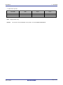
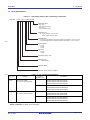
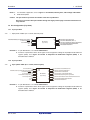
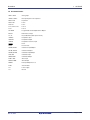
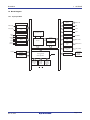
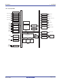
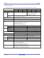
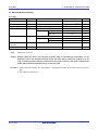
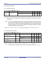
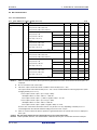
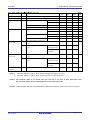
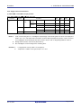
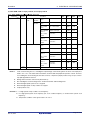
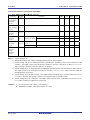
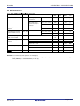
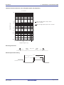
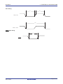
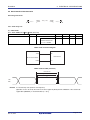
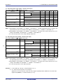
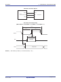
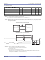
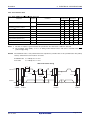
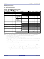
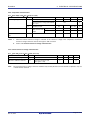
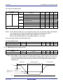
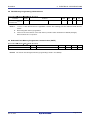
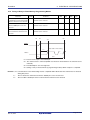
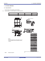
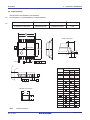
Datasheet RL78/G10 R01DS0207EJ0300 Rev.3.00 Nov 19, 2014 RENESAS MCU True Low Power Platform (as low as 46 µA/MHz), 2.0 to 5.5V Operation, 1 to 4 Kbyte Flash for General Purpose Applications 1. OUTLINE 1.1 Features Ultra-Low Power Technology 2.0 to 5.5 V operation from a single supply Stop (RAM retained): 0.56 µA Operating: 46 µA /MHz Extended-Function Timers Multi-function 16-bit timers: Up to 4 channels Interval timer: 12-bit, 1 channel (only for 16-pin product) 15 kHz watchdog timer : 1 channel RL78-S1 Core Instruction execution: 78 % of instructions can be executed in 1 to 2 clock cycles CISC architecture (Harvard) with 3-stage pipeline Multiply: 8 x 8 to 16-bit result in 2 clock cycles 16-bit barrel shifter for shift & rotate in 2 clock cycle 1-wire on-chip debug function Rich Analog ADC: Up to 7 channels, 10-bit resolution, 3.4 µs conversion time Supports 2.4 V Internal reference voltage (0.815 V (typ.)) Comparator: 1 channel (only for 16-pin product) Main Flash Memory Density: 1 to 4 Kbyte Flash memory rewritable voltage: 4.5 to 5.5 V RAM 128 to 512 Byte size options Supports operands or instructions Back-up retention in all modes High-speed On-chip Oscillator 20 MHz with +/-2 % accuracy over voltage (2.0 to 5.5 V) and temperature (-20 to +85°C) Pre-configured settings: 20 MHz, 10 MHz, 5 MHz, 2.5 MHz, and 1.25 MHz Reset and Supply Management Selectable power-on reset (SPOR) generator with 4 setting options Safety Features Detects execution of illegal instruction Detects watchdog timer program loop General Purpose I/O High-current (up to 20 mA per pin) Open-drain, internal pull-up support External Interrupt External interrupt input: Up to 4 Key interrupt input: 6 Operating Ambient Temperature Standard: -40 to +85°C Package Type and Pin Count SSOP: 10 and 16 pin Multiple Communication Interfaces 2 1 x I C master 1 x I2C multi-master (only for 16-pin product) 1 x UART (7-, 8-bit) Up to 2 x CSI/SPI (7-, 8-bit) R01DS0207EJ0300 Rev.3.00 Nov 19, 2014 Page 1 of 32 RL78/G10 1. OUTLINE ROM, RAM capacities Note Flash ROM RAM 10 pins 16 pins 4 KB 512 B R5F10Y17 R5F10Y47 2 KB 256 B R5F10Y16 R5F10Y46 1 KB 128 B R5F10Y14 R5F10Y44 16-pin products only Remark The functions mounted depend on the product. See 1.6 Outline of Functions. R01DS0207EJ0300 Rev.3.00 Nov 19, 2014 Page 2 of 32 RL78/G10 1. OUTLINE 1.2 List of Part Numbers Figure 1-1. Part Number, Memory Size, and Package of RL78/G10 Part No. R 5 F 1 0 Y 1 6 A S P #V0 Packaging style #V0: Tray #X0: Embossed Tape #30: Tray #50: Embossed Tape Package type: SP: 10-pin, LSSOP, 0.65 mm pitch 16-pin, SSOP, 0.65 mm pitch Classification: A: Consumer applications, operating ambient temperature : -40°C to +85°C D: Industrial applications, operating ambient temperature : -40°C to +85°C <R> ROM capacity: 4: 1 KB 6: 2 KB 7: 4 KB Pin count: 1: 10-pin 4: 16-pin RL78/G10 group: 10Y Memory type: F: Flash memory Renesas MCU Renesas semiconductor product <R> Table 1-1. List of Ordering Part Numbers Pin count Fields of Package Application 10 pins 10-pin plastic LSSOP Part Number Note 1 R5F10Y17ASP#30, R5F10Y17ASP#50 A (4.4 3.6 mm, 0.65 mm pitch) R5F10Y16ASP#V0, R5F10Y16ASP#X0 R5F10Y14ASP#V0, R5F10Y14ASP#X0 D Note 2 R5F10Y17DSP#30, R5F10Y17DSP#50 R5F10Y16DSP#V0, R5F10Y16DSP#X0 R5F10Y14DSP#V0, R5F10Y14DSP#X0 16 pins 16-pin plastic SSOP R5F10Y47ASP#30, R5F10Y47ASP#50 A (4.4 5.0 mm, 0.65 mm pitch) R5F10Y46ASP#30, R5F10Y46ASP#50 R5F10Y44ASP#30, R5F10Y44ASP#50 D Note 2 R5F10Y47DSP#30, R5F10Y47DSP#50 R5F10Y46DSP#30, R5F10Y46DSP#50 R5F10Y44DSP#30, R5F10Y44DSP#50 (Notes and Caution are listed on the next page.) R01DS0207EJ0300 Rev.3.00 Nov 19, 2014 Page 3 of 32 RL78/G10 Notes 1. 2. 1. OUTLINE For the fields of application, refer to Figure 1-1 Part Number, Memory Size, and Package of RL78/G10. Under development Caution The part number represents the number at the time of publication. Be sure to review the latest part number through the target product page in the Renesas Electronics Corp.website. 1.3 Pin Configuration (Top View) 1.3.1 10-pin products <R> 10-pin plastic LSSOP (4.4 × 3.6 mm, 0.65 mm pitch) P40/KR0/TOOL0/(PCLBUZ0)/(TI01/TO01) P125/KR1/RESET P137/TI00/INTP0 VSS VDD 1 2 3 4 5 RL78/G10 (Top View) 10 9 8 7 6 P04/ANI3/TI01/TO01/KR5 P03/ANI2/TO00/KR4/(INTP1) P02/ANI1/SCK00/SCL00/PCLBUZ0/KR3 P01/ANI0/SI00/RXD0/SDA00/KR2 P00/SO00/TXD0/INTP1 Remarks 1. For pin identification, see 1.4 Pin Identification. 2. Functions in parentheses in the above figure can be assigned via settings in the peripheral I/O redirection register (PIOR). See Figure 4-6 Format of Peripheral I/O Redirection Register (PIOR) in the RL78/G10 User’s Manual. 1.3.2 16-pin products <R> 16-pin plastic SSOP (4.4 × 5.0 mm, 0.65 mm pitch) P41/TI03/INTP2 1 16 P07/SDAA0/TO03/ANI6/SCK01 P40/KR0/TOOL0/(PCLBUZ0)/(TI01/TO01) P125/KR1/RESET 2 3 15 14 P06/SCLA0/INTP3/ANI5/SI01 P05/ANI4/TI02/TO02/SO01 P137/TI00/INTP0 4 5 6 13 12 11 P04/ANI3/TI01/TO01/KR5/IVREF0 P03/ANI2/TO00/KR4/(INTP1)/IVCMP0 10 9 P01/ANI0/SI00/RXD0/SDA00/KR2 P00/SO00/TXD0/INTP1 P122/X2/EXCLK/(INTP2) P121/X1/(INTP3) VSS VDD 7 8 RL78/G10 (Top View) P02/ANI1/SCK00/SCL00/PCLBUZ0/KR3/VCOUT0 Remarks 1. For pin identification, see 1.4 Pin Identification. 2. Functions in parentheses in the above figure can be assigned via settings in the peripheral I/O redirection register (PIOR). See Figure 4-6 Format of Peripheral I/O Redirection Register (PIOR) in the RL78/G10 User’s Manual. R01DS0207EJ0300 Rev.3.00 Nov 19, 2014 Page 4 of 32 RL78/G10 1. OUTLINE 1.4 Pin Identification ANI0 to ANI6 : Analog Input INTP0 to INTP3 : Interrupt Request From Peripheral KR0 to KR5 : Key Return P00 to P07 : Port 0 P40, P41 : Port 4 P121, P122, P125 : Port 12 P137 : Port 13 PCLBUZ0 : Programmable Clock Output/ Buzzer Output EXCLK : External Clock Input X1, X2 : Crystal Oscillator (Main System Clock) IVCMP0 : Comparator Input VCOUT0 : Comparator Output IVREF0 : Comparator Reference Input RESET : Reset RxD0 : Receive Data SCK00, SCK01 : Serial Clock Input/Output SCL00, SCLA0 : Serial Clock Output SDA00, SDAA0 : Serial Data Input/Output SI00, SI01 : Serial Data Input SO00, SO01 : Serial Data Output TI00 to TI03 : Timer Input TO00 to TO03 : Timer Output TOOL0 : Data Input/Output for Tool TxD0 : Transmit Data VDD : Power Supply VSS : Ground R01DS0207EJ0300 Rev.3.00 Nov 19, 2014 Page 5 of 32 RL78/G10 1. OUTLINE 1.5 Block Diagram 1.5.1 10-pin products PORT 0 5 P00 to P04 TAU0 (2 ch) TI00 /TO00 ch00 TI01 /TO01 ch01 SAU0 (1 ch) RxD0 TxD0 UART0 SCK00 SI00 SO00 CSI00 SCL00 SDA00 IIC00 TOOL0 PORT 4 P40 PORT 12 P125 PORT 13 P137 Code flash: 4 KB Buzzer/clock output control Interrupt control PCLBUZ0 Key return 6 ch 6 KR0 to KR5 Interrupt control 2 ch 2 INTP0, INTP1 8-/10-bit A/D converter 4 ch 4 ANI0 to ANI3 RL78-S1 RAM 512 B On-chip debugger Clock generator + Reset generator BCD adjustment Selectable power-onreset Low-speed on-chip oscillator 15 kHz VDD R01DS0207EJ0300 Rev.3.00 Nov 19, 2014 RESET Watchdog timer Low-speed on-chip oscillator High-speed on-chip oscillator 1.25 to 20 MHz VSS Page 6 of 32 RL78/G10 1. OUTLINE 1.5.2 16-pin products TAU0 (4 ch) TI00 / TO00 ch00 TI01 / TO01 ch01 TI02 / TO02 ch02 TI03 / TO03 ch03 PORT 0 8 P00 to P07 PORT 4 2 P40, P41 PORT 12 3 P121, P122, P125 PORT 13 SAU0 (1 ch) RxD0 TxD0 UART0 SCK00 SI00 SO00 CSI00 SCK01 SI01 SO01 CSI01 SCL00 SDA00 IIC00 TOOL0 Code flash: 4 KB Buzzer/clock output control Interrupt control RL78-S1 RAM 512 B RESET Clock generator + Reset generator On-chip debugger Main OSC 1 to 20 MHz BCD adjustment SCLA0 SDAA0 IICA0 PCLBUZ0 Key return 6 ch 6 KR0 to KR5 Interrupt control 4 ch 4 INTP0 to INTP3 8-/10-bit A/D converter 7 ch 7 ANI0 to ANI6 Watchdog timer 12-bit interval timer Low-speed on-chip oscillator X1 X2/EXCLK Selectable power-onreset Low-speed on-chip oscillator 15 kHz VDD IVREF0 IVCMP0 VCOUT0 P137 High-speed on-chip oscillator 1.25 to 20 MHz VSS COMP R01DS0207EJ0300 Rev.3.00 Nov 19, 2014 Page 7 of 32 RL78/G10 1. OUTLINE 1.6 Outline of Functions This outline describes the function at the time when Peripheral I/O redirection register (PIOR) is set to 00H. Item 10-pin R5F10Y14 R5F10Y16 16-pin R5F10Y17 Code flash memory 1 KB 2 KB 4 KB RAM 128 B 256 B 512 B Main High-speed system system R5F10Y44 — R5F10Y46 R5F10Y47 1 KB 2 KB 4 KB 128 B 256 B 512 B X1, X2 (crystal/ceramic) oscillation, external clock main system clock input (EXCLK): 1 to 20 MHz: VDD = 2.7 to 5.5 V clock 1 to 5 MHz: VDD = 2.0 to 5.5 V High-speed on-chip oscillator clock Low-speed on-chip oscillator Note 3 1.25 to 20 MHz (VDD = 2.7 to 5.5 V) 1.25 to 5 MHz (VDD = 2.0 to 5.5 V Note 3 ) 15 kHz (TYP) clock General-purpose register 8-bit register 8 Minimum instruction execution 0.05 s (20 MHz operation) time Instruction set Data transfer (8 bits) Adder and subtractor/logical operation (8 bits) Multiplication (8 bits 8 bits) Rotate, barrel shift, and bit manipulation (set, reset, test, and Boolean operation), etc. I/O port Timer Total 8 14 CMOS I/O 6 (N-ch open-drain output (VDD tolerance): 2) 10 (N-ch open-drain output (VDD tolerance): 4) CMOS input 2 4 16-bit timer 2 channels 4 channels Watchdog timer 1 channel 12-bit interval timer — 1 channel Timer output 2 channels (PWM output: 1) 4 channels (PWM outputs: 3 Clock output/buzzer output 1 Comparator — 8-/10-bit resolution A/D converter 4 channels Serial interface [10-pin products] CSI: 1 channel/simplified I C: 1 channel/UART: 1 channel Note 1 ) 2.44 kHz to 10 MHz: (Peripheral hardware clock: fMAIN = 20 MHz operation) 1 7 channels 2 2 [16-pin products] CSI: 2 channels/simplified I C: 1 channel/UART: 1 channel 2 I C bus — 1 channel Vectored Internal 8 14 interrupt External 3 5 sources Key interrupt 6 Reset Reset by RESET pin Internal reset by watchdog timer Internal reset by selectable power-on-reset Internal reset by illegal instruction execution Note 2 Internal reset by data retention lower limit voltage Selectable power-on-reset circuit Detection voltage Rising edge (VSPOR): 2.25 V/2.68 V/3.02 V/4.45 V (max.) Falling edge (VSPDR): 2.20 V/2.62 V/2.96 V/4.37 V (max.) R01DS0207EJ0300 Rev.3.00 Nov 19, 2014 Page 8 of 32 RL78/G10 1. OUTLINE Item 10-pin R5F10Y14 R5F10Y16 On-chip debug function Provided Power supply voltage VDD = 2.0 to 5.5 V Operating ambient temperature TA = - 40 to + 85 C 16-pin R5F10Y17 R5F10Y44 R5F10Y46 R5F10Y47 Note 3 Notes 1. The number of outputs varies, depending on the setting of channels in use and the number of the master 2. The illegal instruction is generated when instruction code FFH is executed. Reset by the illegal instruction 3. Use this product within the voltage range from 2.25 to 5.5 V because the detection voltage (VSPOR) of the (see 6.9.4 Operation as multiple PWM output function in the RL78/G10 User’s Manual). execution not issued by emulation with the on-chip debug emulator. selectable power-on-reset (SPOR) circuit should also be considered. R01DS0207EJ0300 Rev.3.00 Nov 19, 2014 Page 9 of 32 RL78/G10 2. ELECTRICAL SPECIFICATIONS 2. ELECTRICAL SPECIFICATIONS Cautions 1. The RL78 microcontrollers have an on-chip debug function, which is provided for development and evaluation. Do not use the on-chip debug function in products designated for mass production, because the guaranteed number of rewritable times of the flash memory may be exceeded when this function is used, and product reliability therefore cannot be guaranteed. Renesas Electronics is not liable for problems occurring when the on-chip debug function is used. 2. The pins mounted depend on the product. Refer to 2.1 Port Functions and 2.2.1 Functions for each product in the RL78/G10 User’s Manual. 3. Use this product within the voltage range from 2.25 to 5.5 V because the detection voltage (VSPOR) of the selectable power-on-reset (SPOR) circuit should also be considered. R01DS0207EJ0300 Rev.3.00 Nov 19, 2014 Page 10 of 32 RL78/G10 2. ELECTRICAL SPECIFICATIONS 2.1 Absolute Maximum Ratings (TA = 25C) Parameter Symbols Conditions Ratings VDD 0.5 to +6.5 Input Voltage VI1 0.3 to VDD + 0.3 Output Voltage VO1 Output current, high IOH1 Supply Voltage Output current, low IOL1 V V 40 mA P40, P41 70 mA P00 to P07 100 mA Per pin 40 mA P40, P41 70 mA P00 to P07 100 mA TA 40 to +85 C Tstg 65 to +150 C Total of all pins Operating ambient V Note 0.3 to VDD + 0.3 Per pin Total of all pins Unit temperature Storage temperature Note Must be 6.5 V or lower. Caution Product quality may suffer if the absolute maximum rating is exceeded even momentarily for any parameter. That is, the absolute maximum ratings are rated values at which the product is on the verge of suffering physical damage, and therefore the product must be used under conditions that ensure that the absolute maximum ratings are not exceeded. Remarks 1. Unless specified otherwise, the characteristics of alternate-function pins are the same as those of the port pins. 2. The reference voltage is VSS. R01DS0207EJ0300 Rev.3.00 Nov 19, 2014 Page 11 of 32 RL78/G10 2. ELECTRICAL SPECIFICATIONS 2.2 Oscillator Characteristics 2.2.1 X1 oscillator characteristics (TA = 40 to +85C, 2.0 V VDD 5.5 V, VSS = 0 V) Parameter Resonator Conditions MIN. TYP. MAX. Unit X1 clock Ceramic resonator/ 2.7 V VDD 5.5 V 1 20 MHz oscillation crystal resonator 2.0 V VDD < 2.7 V 1 5 MHz frequency (fX) Note Note Indicates only permissible oscillator frequency ranges. Refer to AC Characteristics for instruction execution time. Request evaluation by the manufacturer of the oscillator circuit mounted on a board to check the oscillator characteristics. Caution Since the CPU is started by the high-speed on-chip oscillator clock after a reset release, check the X1 clock oscillation stabilization time using the oscillation stabilization time counter status register (OSTC) by the user. Determine the oscillation stabilization time of the OSTC register and the oscillation stabilization time select register (OSTS) after sufficiently evaluating the oscillation stabilization time with the resonator to be used. Remark When using the X1 oscillator, refer to 5.4 System Clock Oscillator in the RL78/G10 User’s Manual. 2.2.2 On-chip oscillator characteristics (TA = 40 to +85C, 2.0 V VDD 5.5 V, VSS = 0 V) Oscillators High-speed on-chip oscillator oscillation clock frequency Parameters Conditions fIH MIN. TYP. MAX. Unit 1.25 20 MHz Notes 1, 2 High-speed on-chip oscillator oscillation TA = -20 to +85C -2.0 +2.0 % clock frequency accuracy TA = -40 to -20C -3.0 +3.0 % Low-speed on-chip oscillator oscillation fIL 15 kHz clock frequency Low-speed on-chip oscillator oscillation -15 +15 % clock frequency accuracy Notes 1. 2. High-speed on-chip oscillator frequency is selected by bits 0 to 2 of option byte (000C2H). This only indicates the oscillator characteristics. Refer to AC Characteristics for instruction execution time. R01DS0207EJ0300 Rev.3.00 Nov 19, 2014 Page 12 of 32 RL78/G10 2. ELECTRICAL SPECIFICATIONS 2.3 DC Characteristics 2.3.1 Pin characteristics (TA = 40 to +85C, 2.0 V VDD 5.5 V, VSS = 0 V) Parameter Symbol Output current, high IOH1 Note 1 (1/2) Conditions MAX. Unit Per pin for MIN. TYP. -10.0 mA 10-pin products: P00 to P04, P40 Note 2 16-pin products: P00 to P07, P40, P41 Total of 4.0 V VDD 5.5 V -20.0 mA 10-pin products: P40 2.7 V VDD 4.0 V -4.0 mA 16-pin products: P40, P41 2.0 V VDD 2.7 V -3.0 mA Total of 4.0 V VDD 5.5 V -60.0 mA 10-pin products: P00 to P04 2.7 V VDD 4.0 V -12.0 mA 16-pin products: P00 to P07 2.0 V VDD 2.7 V -9.0 mA Total of all pins (When duty 70% Note 3) -80.0 mA Per pin for 20.0 mA 10-pin products: P00 to P04, P40 Note 2 (When duty 70% Note 3) (When duty 70% Note 3) Output current, low IOL1 Note 4 16-pin products: P00 to P07, P40, P41 Total of 4.0 V VDD 5.5 V 40.0 mA 10-pin products: P40 2.7 V VDD 4.0 V 6.0 mA 16-pin products: P40, P41 2.0 V VDD 2.7 V 1.2 mA Total of 4.0 V VDD 5.5 V 80.0 mA 10-pin products: P00 to P04 2.7 V VDD 4.0 V 12.0 mA 16-pin products: P00 to P07 2.0 V VDD 2.7 V 2.4 mA 120.0 mA (When duty 70% Note 3) (When duty 70% Note 3) Total of all pins (When duty 70% Note 3) Notes 1. Value of current at which the device operation is guaranteed even if the current flows from the VDD pin to an output pin. 2. Do not exceed the total current value. 3. This is the output current value under conditions where the duty factor 70%. The output current value when the duty factor 70% can be calculated with the following expression (when changing the duty factor to n%). Total output current of pins = (IOH × 0.7)/(n × 0.01) <Example> Where n = 80 % and IOH = - 10.0 mA Total output current of pins = (- 10.0 × 0.7)/(80 × 0.01) - 8.7 mA Total output current of pins = (IOL × 0.7)/(n × 0.01) <Example> Where n = 80 % and IOL = 10.0 mA Total output current of pins = (10.0 × 0.7)/(80 × 0.01) 8.7 mA However, the current that is allowed to flow into one pin does not vary depending on the duty factor. A current higher than the absolute maximum rating must not flow into one pin. 4. Value of current at which the device operation is guaranteed even if the current flows from an output pin to the VSS pin. Caution P00, P01, P06, and P07 do not output high level in N-ch open-drain mode. Remark Unless specified otherwise, the characteristics of alternate-function pins are the same as those of the port. R01DS0207EJ0300 Rev.3.00 Nov 19, 2014 Page 13 of 32 RL78/G10 2. ELECTRICAL SPECIFICATIONS (TA = 40 to +85C, 2.0 V VDD 5.5 V, VSS = 0 V) Parameter Symbol Input voltage, high VIH1 Input voltage, low VIL1 Output voltage, high VOH1 (2/2) Conditions 4.0 V VDD 5.5 V VOL1 0.8 VDD VDD V 0 0.2 VDD V IOH = -3.0 mA VDD - 0.7 V 2.7 V VDD 5.5 V IOH = -2.0 mA VDD - 0.6 V 2.0 V VDD 5.5 V IOH = -1.5 mA VDD - 0.5 V 4.0 V VDD 5.5 V IOL = 20 mA 1.3 V IOL = 8.5 mA 0.7 V IOL = 3.0 mA 0.6 V IOL = 1.5 mA 0.4 V IOL = 0.6 mA 0.4 V 1 µA 2.0 V VDD 5.5 V current, high Unit V 2.7 V VDD 5.5 V ILIH1 MAX. VDD - 1.5 Note 2 Input leakage TYP. IOH = -10 mA Note 1 Output voltage, low MIN. P00 to P07, P40, P41, P125, P137 VI = VDD ILIH2 P121, P122 (X1, X2, EXCLK) In input port or VI = VDD external clock input 1 In resonator 10 connection ILIL1 Input leakage current, low -1 P00 to P07, P40, P41, P125, P137 µA VI = VSS ILIL2 P121, P122 (X1, X2, EXCLK) In input port or VI = VSS external clock input -1 In resonator -10 connection On-chip pull-up RU VI = VSS 10 20 100 k resistance Notes 1. 2. The value under the condition which satisfies the high-level output current (IOH1). The value under the condition which satisfies the low-level output current (IOL1). Caution The maximum value of VIH of P00, P01, P06, and P07 is VDD even in N-ch open-drain mode. P00, P01, P06, and P07 do not output high level in N-ch open-drain mode. Remark Unless specified otherwise, the characteristics of alternate-function pins are the same as those of the port. R01DS0207EJ0300 Rev.3.00 Nov 19, 2014 Page 14 of 32 RL78/G10 2. ELECTRICAL SPECIFICATIONS 2.3.2 Supply current characteristics (1) Flash ROM: 1 and 2 KB of 10-pin products (TA = 40 to +85C, 2.0 V VDD 5.5 V, VSS = 0 V) Parameter Symbol Supply current IDD1 Note 1 I Note 2 DD2 Note 3 IDD3 Notes 1. Conditions Operating Basic mode operation HALT mode STOP mode MIN. TYP. MAX. fIH = 20 MHz VDD = 3.0 V, 5.0 V 0.91 Normal fIH = 20 MHz VDD = 3.0 V, 5.0 V 1.57 2.04 operation fIH = 5 MHz VDD = 3.0 V, 5.0 V 0.85 1.15 fIH = 20 MHz VDD = 3.0 V, 5.0 V 350 820 fIH = 5 MHz VDD = 3.0 V, 5.0 V 290 600 0.56 2.00 VDD = 3.0 V Unit mA µA µA Total current flowing into VDD, including the input leakage current flowing when the level of the input pin is fixed to VDD or VSS. The values below the MAX. column include the peripheral operation current. However, not including the current flowing into the A/D converter, I/O port, and on-chip pull-up/pull-down resistors. 2. During HALT instruction execution by flash memory. 3. Not including the current flowing into the watchdog timer. Remarks 1. 2. fIH: High-speed on-chip oscillator clock frequency Temperature condition of the typical value is TA = 25C R01DS0207EJ0300 Rev.3.00 Nov 19, 2014 Page 15 of 32 RL78/G10 2. ELECTRICAL SPECIFICATIONS (2) Flash ROM: 4 KB of 10-pin products, and 16-pin products (TA = 40 to +85C, 2.0 V VDD 5.5 V, VSS = 0 V) Parameter Supply current Symbol Note 1 IDD1 Conditions Operating Basic fIH = 20 MHz mode operation Note 4 Normal fIH = 20 MHz operation Note 4 fIH = 5 MHz MIN. TYP. MAX. VDD = 3.0 V, 5.0 V 0.92 VDD = 3.0 V, 5.0 V 1.59 2.14 VDD = 3.0 V, 5.0 V 0.87 1.20 Square wave input 1.43 1.93 Resonator 1.54 2.13 Square wave input 0.67 1.02 Resonator 0.72 1.12 VDD = 3.0 V, 5.0 V 360 900 VDD = 3.0 V, 5.0 V 310 660 Unit mA Note 4 fMX = 20 MHz Notes 5, 6 VDD = 3.0 V, connection 5.0 V fMX = 5 MHz Notes 5, 6 VDD = 3.0 V, 5.0 V I Note 2 DD2 HALT mode fIH = 20 MHz connection µA Note 4 fIH = 5 MHz Note 4 fMX = 20 MHz Square wave input 200 700 Resonator 300 900 Square wave input 100 440 Resonator 150 540 0.61 2.25 Notes 5, 6 VDD = 3.0 V, connection 5.0 V fMX = 5 MHz Notes 5, 6 VDD = 3.0 V, connection 5.0 V I Notes 1. Note 3 DD3 STOP mode VDD = 3.0 V µA Total current flowing into VDD, including the input leakage current flowing when the level of the input pin is fixed to VDD or VSS. The values below the MAX. column include the peripheral operation current. However, not including the current flowing into the A/D converter, comparator (16-pin products only), I/O port, and onchip pull-up/pull-down resistors. 2. During HALT instruction execution by flash memory. 3. Not including the current flowing into the 12-bit interval timer and watchdog timer. 4. When the high-speed system clock is stopped. 5. When the high-speed on-chip oscillator is stopped. 6. 16-pin products only Remarks 1. fIH: High-speed on-chip oscillator clock frequency 2. fMX: High-speed system clock frequency (X1 clock oscillator frequency or external main system clock frequency) 3. Temperature condition of the typical value is TA = 25C R01DS0207EJ0300 Rev.3.00 Nov 19, 2014 Page 16 of 32 RL78/G10 2. ELECTRICAL SPECIFICATIONS (3) Peripheral Functions (Common to all products) (TA = 40 to +85C, 2.0 V VDD 5.5 V, VSS = 0 V) Parameter Symbol Low-speed on- IFIL Conditions MIN. Note 1 TYP. MAX. Unit 0.30 A 0.01 A 0.01 A chip oscillator operating current 12-bit interval ITMKA timer operating Notes 1, 2, 3 current Watchdog timer IWDT operating Notes 1, 4 current A/D converter operating current Notes 1, 5 IADC Comparator operating current Notes 1, 6 ICMP Internal reference voltage operating current IVREG VDD = 5.0 V 1.30 VDD = 3.0 V 0.50 mA In high-speed mode VDD = 5.0 V 6.50 A In low-speed mode VDD = 5.0 V 1.70 A 10 A When conversion at maximum speed Note 1 1.90 mA Notes 1. Current flowing to VDD. 2. When high speed on-chip oscillator and high-speed system clock are stopped. 3. Current flowing only to the 12-bit interval timer (excluding the operating current of the low-speed on-chip oscillator). The supply current of the RL78 microcontrollers is the sum of the values of either IDD1, IDD2 or IDD3 and IFIL and ITMKA, when the 12-bit interval timer is in operation. 4. Current flowing only to the watchdog timer (excluding the operating current of the low-speed on-chip oscillator). The supply current of the RL78 microcontrollers is the sum of IDD1, IDD2 or IDD3 and IFIL and IWDT when the watchdog timer is in operation. 5. Current flowing only to the A/D converter. The supply current of the RL78 microcontrollers is the sum of IDD1 or IDD2 and IADC when the A/D converter operates in an operation mode or the HALT mode. 6. Current flowing only to the comparator. The supply current of the RL78 microcontrollers is the sum of IDD1, IDD2 or IDD3 and ICMP when the comparator is in operation. Remarks 1. fIL: Low-speed on-chip oscillator clock frequency 2. Temperature condition of the typical value is TA = 25C R01DS0207EJ0300 Rev.3.00 Nov 19, 2014 Page 17 of 32 RL78/G10 2. ELECTRICAL SPECIFICATIONS 2.4 AC Characteristics (TA = 40 to +85C, 2.0 V VDD 5.5 V, VSS = 0 V) Items Instruction cycle (minimum Symbol TCY instruction execution time) Conditions MIN. TYP. MAX. Unit When high-speed on- 2.7 V VDD 5.5 V 0.05 0.8 µs chip oscillator clock (fIH) 2.0 V VDD < 2.7 V 0.2 0.8 µs When high-speed 2.7 V VDD 5.5 V 0.05 1.0 µs system clock (fMX) is 2.0 V VDD < 2.7 V 0.2 1.0 µs 2.7 V VDD 5.5 V 1.0 20 MHz 2.0 V VDD < 2.7 V 1.0 5 MHz 2.7 V VDD 5.5 V 24 ns 2.0 V VDD < 2.7 V 95 ns 1/fMCK + ns is selected selected External system clock TEX frequency External system clock input TEXH, TEXL high-level width, low-level width TI00 to TI03 input high-level tTIH, tTIL Noise filter is not used width, low-level width TO00 to TO03 output 10 fTO frequency PCLBUZ0 output frequency RESET low-level width fPCL 4.0 V VDD 5.5 V 10 MHz 2.7 V VDD 4.0 V 5 MHz 2.0 V VDD 2.7 V 2.5 MHz 4.0 V VDD 5.5 V 10 MHz 2.7 V VDD 4.0 V 5 MHz 2.0 V VDD 2.7 V 2.5 MHz tRSL 10 µs Remark fMCK: Timer array unit operation clock frequency (Operation clock to be set by the timer clock select register 0 (TPS0) and the CKS0n1 bit of timer mode register 0nH (TMR0nH). n: Channel number (n = 0 to 3)) R01DS0207EJ0300 Rev.3.00 Nov 19, 2014 Page 18 of 32 RL78/G10 2. ELECTRICAL SPECIFICATIONS Minimum Instruction Execution Time during Main System Clock Operation TCY vs VDD 10 When the high-speed on-chip oscillator clock is selected Cycle time TCY [µs] 1.0 0.8 When the high-speed system clock is selected 0.2 0.1 0.05 0.01 0 1.0 2.0 3.0 2.7 4.0 5.0 6.0 5.5 Supply voltage VDD [V] AC Timing Test Points VIH/VOH VIH/VOH Test points VIL/VOL VIL/VOL External System Clock Timing 1/fEX tEXL tEXH EXCLK R01DS0207EJ0300 Rev.3.00 Nov 19, 2014 Page 19 of 32 RL78/G10 2. ELECTRICAL SPECIFICATIONS TI/TO Timing tTIH tTIL TI00 to TI03 1/fTO TO00 to TO03 RESET Input Timing tRSL RESET R01DS0207EJ0300 Rev.3.00 Nov 19, 2014 Page 20 of 32 RL78/G10 2. ELECTRICAL SPECIFICATIONS 2.5 Serial Interface Characteristics AC Timing Test Points VIH/VOH VIH/VOH Test points VIL/VOL VIL/VOL 2.5.1 Serial array unit (1) UART mode (TA = 40 to +85C, 2.0 V VDD 5.5 V, VSS = 0 V) Parameter Symbol Conditions MIN. Transfer rate Theoretical value of the TYP. MAX. Unit fMCK/6 bps 3.3 Mbps maximum transfer rate fCLK = fMCK = 20 MHz UART mode connection diagram Rx TxD0 User's device RL78 microcontroller RxD0 Tx UART mode bit width (reference) 1/Transfer rate High-/Low-bit width Baud rate error tolerance TxD0 RxD0 Remark fMCK: Serial array unit operation clock frequency (Operation clock to be set by the serial clock select register 0 (SPS0) and the CKS0n bit of the serial mode register 0nH (SMR0nH). n: Channel number (n = 0, 1)) R01DS0207EJ0300 Rev.3.00 Nov 19, 2014 Page 21 of 32 RL78/G10 2. ELECTRICAL SPECIFICATIONS (2) CSI mode (master mode, SCKp... internal clock output) (TA = 40 to +85C, 2.0 V VDD 5.5 V, VSS = 0 V) Parameter Symbol Conditions MIN. 2.7 V VDD 5.5 V TYP. MAX. Unit SCKp cycle time tKCY1 tKCY1 4/fCLK 800 ns SCKp high-/low-level width tKH1, tKL1 2.7 V VDD 5.5 V tKCY1/2 - 18 ns 2.0 V VDD 5.5 V tKCY1/2 - 50 ns 2.7 V VDD 5.5 V 47 ns 2.0 V VDD 5.5 V 110 ns 19 ns 200 2.0 V VDD 5.5 V SIp setup time (to SCKp) Note 1 SIp hold time (from SCKp) Note 1 Delay time from SCKp to SOp output tSIK1 tKSI1 tKSO1 C = 30 pF ns Note 3 25 ns Note 2 Notes 1. When DAP0n = 0 and CKP0n = 0, or DAP0n = 1 and CKP0n = 1. The SIp setup time becomes “to SCKp” and SIp hold time becomes “from SCKp” when DAP0n = 0 and CKP0n = 1, or DAP0n = 1 and CKP0n = 0. 2. When DAP0n = 0 and CKP0n = 0, or DAP0n = 1 and CKP0n = 1. The delay time to SOp output becomes “from SCKp” when DAP0n = 0 and CKP0n = 1, or DAP0n = 1 and CKP0n = 0. 3. C is the load capacitance of the SCKp and SOp output lines. (3) CSI mode (slave mode, SCKp... external clock input) (TA = 40 to +85C, 2.0 V VDD 5.5 V, VSS = 0 V) Parameter Symbol SCKp cycle time <R> tKCY2 SCKp high-/low-level width tKH2, Conditions 2.7 V VDD 5.5 V MIN. TYP. MAX. Unit fMCK > 16 MHz 8/fMCK ns fMCK 16 MHz 6/fMCK ns 2.0 V VDD 5.5 V 6/fMCK ns 2.0 V VDD 5.5 V tKCY2/2 - 18 ns 2.7 V VDD 5.5 V 1/fMCK + 20 ns 2.0 V VDD 5.5 V 1/fMCK + 30 ns 2.0 V VDD 5.5 V 1/fMCK + 31 ns tKL2 Note 1 SIp setup time (to SCKp) SIp hold time (from SCKp) Note 1 Delay time from SCKp to SOp output tSIK2 tKSI2 tKSO2 C = 30 pF Note 3 Note 2 2.7 V VDD 5.5 V 2/fMCK + 50 ns 2.0 V VDD 5.5 V 2/fMCK + 110 ns Notes 1. When DAP0n = 0 and CKP0n = 0, or DAP0n = 1 and CKP0n = 1. The SIp setup time becomes “to SCKp” and the SIp hold time becomes “from SCKp” when DAP0n = 0 and CKP0n = 1, or DAP0n = 1 and CKP0n = 0. 2. When DAP0n = 0 and CKP0n = 0, or DAP0n = 1 and CKP0n = 1. The delay time to SOp output becomes “from SCKp” when DAP0n = 0 and CKP0n = 1, or DAP0n = 1 and CKP0n = 0. 3. C is the load capacitance of the SOp output lines. Remarks 1. p: CSI number (p = 00, 01), n: Channel number (n = 0, 1) 2. fMCK: Serial array unit operation clock frequency (Operation clock to be set by the serial clock select register 0 (SPS0) and the CKS0n bit of the serial mode register 0nH (SMR0nH). n: Channel number (n = 0, 1)) R01DS0207EJ0300 Rev.3.00 Nov 19, 2014 Page 22 of 32 RL78/G10 2. ELECTRICAL SPECIFICATIONS CSI mode connection diagram SCK SCK00 RL78 SI00 microcontroller SO SO00 User's device SI CSI mode serial transfer timing (When DAP0n = 0 and CKP0n = 0, or DAP0n = 1 and CKP0n = 1.) t KCY1, 2 t KL1, 2 t KH1, 2 SCK00 t SIK1, 2 SI00 t KSI1, 2 Input data t KSO1, 2 SO00 Remark Output data p: CSI number (p = 00, 01), n: Channel number (n = 0, 1) R01DS0207EJ0300 Rev.3.00 Nov 19, 2014 Page 23 of 32 RL78/G10 2. ELECTRICAL SPECIFICATIONS 2 (4) Simplified I C mode (TA = 40 to +85C, 2.0 V VDD 5.5 V, VSS = 0 V) Parameter Symbol Conditions MIN. MAX. 400 Note 1 Unit SCLr clock frequency fSCL Cb = 100 pF, Rb = 3 k Hold time when SCLr = "L" tLOW Cb = 100 pF, Rb = 3 k 1150 ns Hold time when SCLr = "H" tHIGH Cb = 100 pF, Rb = 3 k 1150 ns Data setup time (reception) tSU: DAT Cb = 100 pF, Rb = 3 k 1/fMCK + ns 145 Data hold time (transmission) Notes 1. 2. tHD: DAT Cb = 100 pF, Rb = 3 k kHz Note 2 0 355 ns The value must also be equal to or less than fMCK/4. Set the fMCK value to keep the hold time of SCLr = "L" and SCLr = "H". Caution Select the N-ch open drain output (VDD tolerance) mode for the SDAr pin by using the port output mode register 0 (POM0). 2 Simplified I C mode connection diagram Vb Rb SDA SDA00 RL78 microcontroller User's device SCL SCL00 2 Simplified I C mode serial transfer timing 1/fSCL tLOW tHIGH SCL00 SDA00 tHD:DAT tSU:DAT Remarks 1. Rb []: Communication line (SDAr) pull-up resistance, Cb [F]: Communication line (SCLr, SDAr) load capacitance 2. r: IIC number (r = 00) 3. fMCK: Serial array unit operation clock frequency (Operation clock to be set by the serial clock select register 0 (SPS0) and the CKS0n bit of the serial mode register 0nH (SMR0nH). n: Channel number (n = 0)) R01DS0207EJ0300 Rev.3.00 Nov 19, 2014 Page 24 of 32 RL78/G10 2. ELECTRICAL SPECIFICATIONS 2.5.2 Serial interface IICA (TA = 40 to +85C, 2.0 V VDD 5.5 V, VSS = 0 V) Parameter Symbol Conditions Standard Mode MIN. SCLA0 clock frequency fSCL Fast mode: fCLK 3.5 MHz Standard mode: fCLK 1 MHz Setup time of restart condition MAX. 0 Fast Mode MIN. MAX. 0 400 100 Unit kHz kHz tSU:STA 4.7 0.6 s tHD:STA 4.0 0.6 s Hold time when SCLA0 = “L” tLOW 4.7 1.3 s Hold time when SCLA0 = “H” tHIGH 4.0 0.6 s tSU:DAT 250 100 ns Data hold time (transmission) tHD:DAT 0 Setup time of stop condition tSU:STO 4.0 0.6 s Bus-free time tBUF 4.7 1.3 s Hold time Note 1 Data setup time (reception) Note 2 Notes 1. 2. Remark 3.45 0 0.9 s The first clock pulse is generated after this period when the start/restart condition is detected. The maximum value (MAX.) of tHD:DAT is during normal transfer and a wait state is inserted in the ACK (acknowledge) timing. The maximum value of Cb (communication line capacitance) and the value of Rb (communication line pull-up resistor) at that time in each mode are as follows. Standard mode: Cb = 400 pF, Rb = 2.7 k Fast mode: Cb = 200 pF, Rb = 1.7 k IICA serial transfer timing tLOW tR SCLA0 tHD:DAT tHD:STA tHIGH tF tSU:STA tHD:STA tSU:STO tSU:DAT SDAA0 tBUF Stop condition Start condition R01DS0207EJ0300 Rev.3.00 Nov 19, 2014 Restart condition Stop condition Page 25 of 32 RL78/G10 2. ELECTRICAL SPECIFICATIONS 2.6 Analog Characteristics 2.6.1 A/D converter characteristics (Target pin: ANI0 to ANI6, internal reference voltage) (TA = 40 to +85C, 2.4 V VDD 5.5 V, VSS = 0 V) Parameter Symbol Resolution Conditions MIN. RES Notes 1, 2, 3 Overall error AINL Conversion time tCONV TYP. 8 10-bit resolution MAX. Unit 10 bit VDD = 5 V 1.7 3.1 LSB VDD = 3 V 2.3 4.5 LSB 3.4 18.4 µs 4.6 18.4 µs 4.6 18.4 µs VDD = 5 V 0.19 %FSR VDD = 3 V 0.39 %FSR VDD = 5 V 0.29 %FSR VDD = 3 V 0.42 %FSR VDD = 5 V 1.8 LSB VDD = 3 V 1.7 LSB VDD = 5 V 1.4 LSB VDD = 3 V 1.5 LSB VDD V 10-bit resolution 2.7 V VDD 5.5 V Target pin: ANI0 2.4 V VDD 5.5 V Note 5 to ANI6 10-bit resolution 2.4 V VDD 5.5 V Target pin: internal reference voltage Notes 1, 2, 3, 4 Zero-scale error Full-scale error Notes 1, 2, 3, 4 Integral linearity error Notes 1, 2, 3 Differential linearity error EZS EFS ILE DLE Note 6 10-bit resolution 10-bit resolution 10-bit resolution 10-bit resolution Notes 1, 2, 3 Analog input voltage VAIN Target pin: ANI0 to ANI6 Target pin: internal reference voltage 0 Note 6 VREG Note 7 V Notes 1. TYP. Value is the average value at TA = 25C. MAX. value is the average value 3σ at normal distribution. 2. These values are the results of characteristic evaluation and are not checked for shipment. 3. Excludes quantization error (1/2 LSB). 4. This value is indicated as a ratio (%FSR) to the full-scale value. 5. Set the LV0 bit in the A/D converter mode register 0 (ADM0) to 0 when conversion is done in the operating voltage range of 2.4 V ≤ VDD < 2.7 V. 6. Set the LV0 bit in the A/D converter mode register 0 (ADM0) to 0 when the internal reference voltage is selected as the target for conversion. 7. Refer to 2.6.3 Internal reference voltage characteristics. Cautions 1. Arrange wiring and insert the capacitor so that no noise appears on the power supply/ground line. 2. Do not allow any pulses that rapidly change such as digital signals to be input/output to/from the pins adjacent to the conversion pin during A/D conversion. 3. Note that the internal reference voltage cannot be used as the reference voltage of the comparator when the internal reference voltage is selected as the target for A/D conversion. R01DS0207EJ0300 Rev.3.00 Nov 19, 2014 Page 26 of 32 RL78/G10 2. ELECTRICAL SPECIFICATIONS 2.6.2 Comparator characteristics (TA = 40 to +85C, 2.0 V VDD 5.5 V, VSS = 0 V) Parameter Input voltage range Symbol IVREF Conditions IVREF0 pin input (when C0VFR bit = 0) MIN. 0 Internal reference voltage (when C0VRF bit = 1) Output delay TYP. VREG MAX. Unit VDD - 1.4 V Note 2 V Note 1 IVCMP IVCMP0 pin input -0.3 td VDD = 3.0 V, High-speed mode input slew rate > 50 Low-speed mode VDD + 0.3 V 0.5 µs 2.0 µs mV/µs Operation stabilization wait tCMP 100 µs time Notes 1. 2. When the internal reference voltage is selected as the reference voltage of the comparator, the internal reference voltage cannot be used as the target for A/D conversion. Refer to 2.6.3 Internal reference voltage characteristics. 2.6.3 Internal reference voltage characteristics (TA = 40 to +85C, 2.0 V VDD 5.5 V, VSS = 0 V) Parameter Symbol Internal reference voltage VREG Operation stabilization wait time tAMP Conditions When A/D converter is used MIN. TYP. MAX. Unit 0.74 0.815 0.89 V 5 µs (ADS register = 07H) Note The internal reference voltage cannot be simultaneously used by the A/D converter and the comparator; only one of them must be selected. R01DS0207EJ0300 Rev.3.00 Nov 19, 2014 Page 27 of 32 RL78/G10 2. ELECTRICAL SPECIFICATIONS 2.6.4 SPOR circuit characteristics (TA = 40 to +85C, VSS = 0 V) Parameter Symbol Detection Power supply voltage voltage level MIN. TYP. MAX. Unit Power supply rise time 4.08 4.28 4.45 V Power supply fall time 4.00 4.20 4.37 V VSPOR1 Power supply rise time 2.76 2.90 3.02 V Power supply fall time 2.70 2.84 2.96 V VSPOR2 Power supply rise time 2.44 2.57 2.68 V Power supply fall time 2.40 2.52 2.62 V Power supply rise time 2.05 2.16 2.25 V Power supply fall time 2.00 2.11 2.20 V VSPOR0 VSPOR3 Minimum pulse width Note Note Conditions TLSPW 300 µs Time required for the reset operation by the SPOR when VDD becomes under VSPOR. Caution Set the detection voltage (VSPOR) in the operating voltage range. The operating voltage range depends on the setting of the user option byte (000C2H). The operating voltage range is as follows: When the CPU operating frequency is from 1 MHz to 20 MHz: VDD = 2.7 to 5.5 V When the CPU operating frequency is from 1 MHz to 5 MHz: VDD = 2.0 to 5.5 V 2.6.5 Power supply voltage rising slope characteristics (TA = 40 to +85C, VSS = 0 V) Parameter Power supply voltage rising slope Symbol Conditions MIN. TYP. SVDD MAX. Unit 54 V/ms MAX. Unit 5.5 V <R> 2.7 RAM Data Retention Characteristics (TA = 40 to +85C, VSS = 0 V) Parameter Data retention power supply voltage Symbol Conditions VDDDR MIN. 1.9 TYP. Caution Data in RAM is retained until the power supply voltage becomes under the minimum value of the data retention power supply voltage (VDDDR). Note that data in the RESF register might not be cleared even if the power supply voltage becomes under the minimum value of the data retention power supply voltage (VDDDR). STOP mode SPOR reset period (Retain data in RAM and RESF) Normal operation V DD Rising of V SPOR STOP instruction execution Falling of V SPDR VDDDR R01DS0207EJ0300 Rev.3.00 Nov 19, 2014 Page 28 of 32 RL78/G10 2. ELECTRICAL SPECIFICATIONS 2.8 Flash Memory Programming Characteristics (TA = 0 to + 40C, 4.5 V VDD 5.5 V, VSS = 0 V) Parameter Code flash memory rewritable times Notes 1. Symbol Cerwr Conditions Retained for 20 years. MIN. TA = +85C TYP. MAX. 1000 Unit Times Notes 1, 2, 3 1 erase + 1 write after the erase is regarded as 1 rewrite. The retaining years are until next rewrite after the rewrite. 2. When using flash memory programmer. 3. These are the characteristics of the flash memory and the results obtained from reliability testing by Renesas Electronics Corporation. 2.9 Dedicated Flash Memory Programmer Communication (UART) (TA = 0 to + 40C, 4.5 V VDD 5.5 V, VSS = 0 V) Parameter Symbol Conditions MIN. Transfer rate Remark TYP. 115,200 MAX. Unit bps The transfer rate during flash memory programming is fixed to 115,200 bps. R01DS0207EJ0300 Rev.3.00 Nov 19, 2014 Page 29 of 32 RL78/G10 2. ELECTRICAL SPECIFICATIONS 2.10 Timing of Entry to Flash Memory Programming Modes Parameter Symbol Time to complete the tSUINIT Conditions MIN. TYP. SPOR reset must be released before the MAX. Unit 100 ms external reset is released. communication for the initial setting after the external reset is released Time to release the external reset tSU SPOR reset must be released before the 10 µs 1 ms external reset is released. after the TOOL0 pin is set to the low level Time to hold the TOOL0 pin at the tHD low level after the external reset is SPOR reset must be released before the external reset is released. released <1> <2> <4> <3> RESET t HD 1-byte data for mode setting TOOL0 t SU t SUINIT <1> The low level is input to the TOOL0 pin. <2> The external reset is released (SPOR reset must be released before the external reset is released.). <3> The TOOL0 pin is set to the high level. <4> Setting of entry to the flash memory programming mode by UART reception is completed. Remark tSUINIT: Communication for the initial setting must be completed within 100 ms after the external reset is released during this period. tSU: Time to release the external reset after the TOOL0 pin is set to the low level tHD: Time to hold the TOOL0 pin at the low level after the external reset is released R01DS0207EJ0300 Rev.3.00 Nov 19, 2014 Page 30 of 32 RL78/G10 3. PACKAGE DRAWINGS 3. PACKAGE DRAWINGS 3.1 10-pin products R5F10Y17ASP, R5F10Y16ASP, R5F10Y14ASP <R> R5F10Y17DSP Note, R5F10Y16DSP Note, R5F10Y14DSP Note JEITA Package Code RENESAS Code Previous Code MASS (TYP.) [g] P-LSSOP10-4.4x3.6-0.65 PLSP0010JA-A P10MA-65-CAC-2 0.05 V detail of lead end 6 10 T I P 5 1 L U V A W W F H G J S E B C N S D M M NOTE Each lead centerline is located within 0.13 mm of its true position (T.P.) at maximum material condition. K (UNIT:mm) ITEM A B DIMENSIONS 3.60 ±0.10 0.50 C 0.65 (T.P.) D 0.24 ± 0.08 E 0.10 ± 0.05 F 1.45 MAX. G 1.20 ± 0.10 H I 6.40 ± 0.20 4.40 ± 0.10 L 1.00 ± 0.20 + 0.08 0.17 − 0.07 0.50 M 0.13 N 0.10 J K T +5 ° 3° 3 ° − 0.25 (T.P.) U 0.60 ± 0.15 V 0.25 MAX. W 0.15 MAX. P 2012 Renesas Electronics Corporation. All rights reserved. Note Under development R01DS0207EJ0300 Rev.3.00 Nov 19, 2014 Page 31 of 32 RL78/G10 3. PACKAGE DRAWINGS 3.2 16-pin products R5F10Y47ASP, R5F10Y46ASP, R5F10Y44ASP <R> R5F10Y47DSP Note, R5F10Y46DSP Note, R5F10Y44DSP Note JEITA Package code RENESAS code Previous code MASS(TYP.)[g] P-SSOP16-4.4x5-0.65 PRSP0016JC-B P16MA-65-FAB-1 0.08 <R> D1 D detail of lead end L1 9 16 B INDEX MARK 1 E HE c 8 L ZD A bp x M S AB A Referance Symbol A2 S Dimension in Millimeters Min e y S D 4.85 5.00 5.15 5.05 5.20 5.35 E 4.20 4.40 4.60 0.075 0.125 0.17 0.24 0.14 0.17 A1 1.50 A bp c b1 c1 c 0.20 0.15 θ 0° HE 6.20 e 8° 6.40 6.60 0.65 x 0.13 y 0.10 ZD L L1 Note 0.32 0.22 c1 bp 0.175 1.725 b1 Terminal cross section Max D1 A2 A1 Nom 0.225 0.35 0.50 0.65 1.00 Under development R01DS0207EJ0300 Rev.3.00 Nov 19, 2014 Page 32 of 32 Revision History RL78/G10 Datasheet Description Rev. Date Page Summary 1.00 2.00 Apr 15, 2013 Jan 10, 2014 1, 2 3 4 8, 9 11 12 13, 14 First Edition issued Modification of descriptions in 1.1 Features Modification of description in 1.2 List of Part Numbers Modification of remark 2 in 1.3.1 10-pin products and 1.3.2 16-pin products Addition of description of R5F10Y17ASP in 1.6 Outline of Functions Modification of description in 2.1 Absolute Maximum Ratings Modification of description in 2.2 Oscillator Characteristics Modification of description, notes 1 to 4, and caution in 2.3.1 Pin characteristics Addition of description, notes 1 to 6, and remarks 1 and 2 in (2) Flash ROM: 4 KB of 10-pin products, and 16-pin products Addition of description, notes 1 to 6, and remarks 1 to 3 in (3) Peripheral Functions (Common to all products) Modification of description in 2.4 AC Characteristics Addition of figure of Minimum Instruction Execution Time during Main System Clock Operation Addition of figure of External System Clock Timing Modification of TI/TO Timing Addition of description in 2.5.2 Serial interface IICA Modification of description and notes 1 to 6 in 2.6.1 A/D converter characteristics Addition of description, notes 1 and 2 in 2.6.2 Comparator characteristics Addition of description and note in 2.6.3 Internal reference voltage characteristics Addition of caution in 2.6.4 SPOR Circuit characteristics Addition of figure in 2.6.6 Data retention power supply voltage characteristics Addition of R5F10Y17ASP in 3.1 10-pin products Modification of package drawing in 3.2 16-pin products Addition of industrial applications in Figure 1-1 Part Number, Memory Size, and Package of RL78/G10 Addition of industrial applications in Table 1-1 List of Ordering Part Numbers Addition of description to pin configuration in 1.3.1 10-pin products and 1.3.2 16-pin products Correction of error in 2.5.1 Serial array unit, (3) CSI mode (slave mode, SCKp... external clock input) Renamed to 2.7 RAM Data Retention Characteristics and modification of figure Addition of industrial application in 3.1 10-pin products Addition of industrial application in 3.2 16-pin products and modification of package drawing 16 17 18 19 19 20 25 26 27 27 3.00 Nov 19, 2014 28 28 31 32 3 3 4 22 28 31 32 All trademarks and registered trademarks are the property of their respective owners. SuperFlash is a registered trademark of Silicon Storage Technology, Inc. in several countries including the United States and Japan. Caution: This product uses SuperFlash® technology licensed from Silicon Storage Technology, Inc. C-1 NOTES FOR CMOS DEVICES (1) VOLTAGE APPLICATION WAVEFORM AT INPUT PIN: Waveform distortion due to input noise or a reflected wave may cause malfunction. If the input of the CMOS device stays in the area between VIL (MAX) and VIH (MIN) due to noise, etc., the device may malfunction. Take care to prevent chattering noise from entering the device when the input level is fixed, and also in the transition period when the input level passes through the area between VIL (MAX) and VIH (MIN). (2) HANDLING OF UNUSED INPUT PINS: Unconnected CMOS device inputs can be cause of malfunction. If an input pin is unconnected, it is possible that an internal input level may be generated due to noise, etc., causing malfunction. CMOS devices behave differently than Bipolar or NMOS devices. Input levels of CMOS devices must be fixed high or low by using pull-up or pull-down circuitry. Each unused pin should be connected to VDD or GND via a resistor if there is a possibility that it will be an output pin. All handling related to unused pins must be judged separately for each device and according to related specifications governing the device. (3) PRECAUTION AGAINST ESD: A strong electric field, when exposed to a MOS device, can cause destruction of the gate oxide and ultimately degrade the device operation. Steps must be taken to stop generation of static electricity as much as possible, and quickly dissipate it when it has occurred. Environmental control must be adequate. When it is dry, a humidifier should be used. It is recommended to avoid using insulators that easily build up static electricity. Semiconductor devices must be stored and transported in an anti-static container, static shielding bag or conductive material. All test and measurement tools including work benches and floors should be grounded. The operator should be grounded using a wrist strap. Semiconductor devices must not be touched with bare hands. Similar precautions need to be taken for PW boards with mounted semiconductor devices. (4) STATUS BEFORE INITIALIZATION: Power-on does not necessarily define the initial status of a MOS device. Immediately after the power source is turned ON, devices with reset functions have not yet been initialized. Hence, power-on does not guarantee output pin levels, I/O settings or contents of registers. A device is not initialized until the reset signal is received. A reset operation must be executed immediately after power-on for devices with reset functions. (5) POWER ON/OFF SEQUENCE: In the case of a device that uses different power supplies for the internal operation and external interface, as a rule, switch on the external power supply after switching on the internal power supply. When switching the power supply off, as a rule, switch off the external power supply and then the internal power supply. Use of the reverse power on/off sequences may result in the application of an overvoltage to the internal elements of the device, causing malfunction and degradation of internal elements due to the passage of an abnormal current. The correct power on/off sequence must be judged separately for each device and according to related specifications governing the device. (6) INPUT OF SIGNAL DURING POWER OFF STATE : Do not input signals or an I/O pull-up power supply while the device is not powered. The current injection that results from input of such a signal or I/O pull-up power supply may cause malfunction and the abnormal current that passes in the device at this time may cause degradation of internal elements. Input of signals during the power off state must be judged separately for each device and according to related specifications governing the device. Notice 1. Descriptions of circuits, software and other related information in this document are provided only to illustrate the operation of semiconductor products and application examples. You are fully responsible for the incorporation of these circuits, software, and information in the design of your equipment. Renesas Electronics assumes no responsibility for any losses incurred by you or third parties arising from the use of these circuits, software, or information. 2. Renesas Electronics has used reasonable care in preparing the information included in this document, but Renesas Electronics does not warrant that such information is error free. Renesas Electronics 3. Renesas Electronics does not assume any liability for infringement of patents, copyrights, or other intellectual property rights of third parties by or arising from the use of Renesas Electronics products or assumes no liability whatsoever for any damages incurred by you resulting from errors in or omissions from the information included herein. technical information described in this document. No license, express, implied or otherwise, is granted hereby under any patents, copyrights or other intellectual property rights of Renesas Electronics or others. 4. You should not alter, modify, copy, or otherwise misappropriate any Renesas Electronics product, whether in whole or in part. Renesas Electronics assumes no responsibility for any losses incurred by you or 5. Renesas Electronics products are classified according to the following two quality grades: "Standard" and "High Quality". The recommended applications for each Renesas Electronics product depends on third parties arising from such alteration, modification, copy or otherwise misappropriation of Renesas Electronics product. the product's quality grade, as indicated below. "Standard": Computers; office equipment; communications equipment; test and measurement equipment; audio and visual equipment; home electronic appliances; machine tools; personal electronic equipment; and industrial robots etc. "High Quality": Transportation equipment (automobiles, trains, ships, etc.); traffic control systems; anti-disaster systems; anti-crime systems; and safety equipment etc. Renesas Electronics products are neither intended nor authorized for use in products or systems that may pose a direct threat to human life or bodily injury (artificial life support devices or systems, surgical implantations etc.), or may cause serious property damages (nuclear reactor control systems, military equipment etc.). You must check the quality grade of each Renesas Electronics product before using it in a particular application. You may not use any Renesas Electronics product for any application for which it is not intended. Renesas Electronics shall not be in any way liable for any damages or losses incurred by you or third parties arising from the use of any Renesas Electronics product for which the product is not intended by Renesas Electronics. 6. You should use the Renesas Electronics products described in this document within the range specified by Renesas Electronics, especially with respect to the maximum rating, operating supply voltage range, movement power voltage range, heat radiation characteristics, installation and other product characteristics. Renesas Electronics shall have no liability for malfunctions or damages arising out of the use of Renesas Electronics products beyond such specified ranges. 7. Although Renesas Electronics endeavors to improve the quality and reliability of its products, semiconductor products have specific characteristics such as the occurrence of failure at a certain rate and malfunctions under certain use conditions. Further, Renesas Electronics products are not subject to radiation resistance design. Please be sure to implement safety measures to guard them against the possibility of physical injury, and injury or damage caused by fire in the event of the failure of a Renesas Electronics product, such as safety design for hardware and software including but not limited to redundancy, fire control and malfunction prevention, appropriate treatment for aging degradation or any other appropriate measures. Because the evaluation of microcomputer software alone is very difficult, please evaluate the safety of the final products or systems manufactured by you. 8. Please contact a Renesas Electronics sales office for details as to environmental matters such as the environmental compatibility of each Renesas Electronics product. Please use Renesas Electronics products in compliance with all applicable laws and regulations that regulate the inclusion or use of controlled substances, including without limitation, the EU RoHS Directive. Renesas Electronics assumes no liability for damages or losses occurring as a result of your noncompliance with applicable laws and regulations. 9. Renesas Electronics products and technology may not be used for or incorporated into any products or systems whose manufacture, use, or sale is prohibited under any applicable domestic or foreign laws or regulations. You should not use Renesas Electronics products or technology described in this document for any purpose relating to military applications or use by the military, including but not limited to the development of weapons of mass destruction. When exporting the Renesas Electronics products or technology described in this document, you should comply with the applicable export control laws and regulations and follow the procedures required by such laws and regulations. 10. It is the responsibility of the buyer or distributor of Renesas Electronics products, who distributes, disposes of, or otherwise places the product with a third party, to notify such third party in advance of the contents and conditions set forth in this document, Renesas Electronics assumes no responsibility for any losses incurred by you or third parties as a result of unauthorized use of Renesas Electronics products. 11. This document may not be reproduced or duplicated in any form, in whole or in part, without prior written consent of Renesas Electronics. 12. Please contact a Renesas Electronics sales office if you have any questions regarding the information contained in this document or Renesas Electronics products, or if you have any other inquiries. (Note 1) "Renesas Electronics" as used in this document means Renesas Electronics Corporation and also includes its majority-owned subsidiaries. (Note 2) "Renesas Electronics product(s)" means any product developed or manufactured by or for Renesas Electronics. http://www.renesas.com SALES OFFICES Refer to "http://www.renesas.com/" for the latest and detailed information. Renesas Electronics America Inc. 2880 Scott Boulevard Santa Clara, CA 95050-2554, U.S.A. Tel: +1-408-588-6000, Fax: +1-408-588-6130 Renesas Electronics Canada Limited 1101 Nicholson Road, Newmarket, Ontario L3Y 9C3, Canada Tel: +1-905-898-5441, Fax: +1-905-898-3220 Renesas Electronics Europe Limited Dukes Meadow, Millboard Road, Bourne End, Buckinghamshire, SL8 5FH, U.K Tel: +44-1628-651-700, Fax: +44-1628-651-804 Renesas Electronics Europe GmbH Arcadiastrasse 10, 40472 Düsseldorf, Germany Tel: +49-211-65030, Fax: +49-211-6503-1327 Renesas Electronics (China) Co., Ltd. 7th Floor, Quantum Plaza, No.27 ZhiChunLu Haidian District, Beijing 100083, P.R.China Tel: +86-10-8235-1155, Fax: +86-10-8235-7679 Renesas Electronics (Shanghai) Co., Ltd. Unit 301, Tower A, Central Towers, 555 LanGao Rd., Putuo District, Shanghai, China Tel: +86-21-2226-0888, Fax: +86-21-2226-0999 Renesas Electronics Hong Kong Limited Unit 1601-1613, 16/F., Tower 2, Grand Century Place, 193 Prince Edward Road West, Mongkok, Kowloon, Hong Kong Tel: +852-2886-9318, Fax: +852 2886-9022/9044 Renesas Electronics Taiwan Co., Ltd. 13F, No. 363, Fu Shing North Road, Taipei, Taiwan Tel: +886-2-8175-9600, Fax: +886 2-8175-9670 Renesas Electronics Singapore Pte. Ltd. 80 Bendemeer Road, Unit #06-02 Hyflux Innovation Centre Singapore 339949 Tel: +65-6213-0200, Fax: +65-6213-0300 Renesas Electronics Malaysia Sdn.Bhd. Unit 906, Block B, Menara Amcorp, Amcorp Trade Centre, No. 18, Jln Persiaran Barat, 46050 Petaling Jaya, Selangor Darul Ehsan, Malaysia Tel: +60-3-7955-9390, Fax: +60-3-7955-9510 Renesas Electronics Korea Co., Ltd. 12F., 234 Teheran-ro, Gangnam-Gu, Seoul, 135-080, Korea Tel: +82-2-558-3737, Fax: +82-2-558-5141 © 2014 Renesas Electronics Corporation. All rights reserved. Colophon 3.0