1
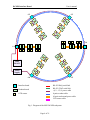
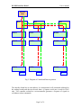
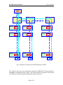
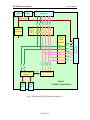
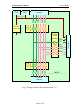
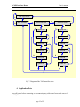
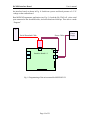
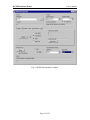
ENDCAP Alignment
CMS CCD OPTICAL POSITION SENSOR
INTERFACE BOARD
User’s Manual
FNAL – PNPI
2003
DCOPS Interface Board
User’s manual
Contents
1. Introduction
3
2. Construction
7
3. Circuit Diagram
11
4. Application Notes
12
5. Functioning
13
6. CPLD Programming
13
7. Debugging and Testing
16
8. Troubleshooting and Maintenance
18
9.
20
Specification
Page 2 of 21
DCOPS Interface Board
User’s manual
1. Introduction
The DCOPS interface boards provide the following features for each chamber layer:
• Low voltage distribution between other interface boards (periphery link),
• Low voltage distribution to a group of the readout board (radial link),
• RS-422 / LVDS interface for DAQ (both periphery and radial links),
• RS-422 / LVDS interface for JTAG (both periphery and radial links),
• Test Access Port (TAP) control.
Intended for the work with long cables the interface boards perform the conditioning of
signals.
To understand purpose of the interface boards it is necessary to issue from a general
organization of the DCOPS readout subsystem. Its structure for the ME2 chamber layer is
shown in Fig. 1. Other subsystems contain various numbers of elements, but they are
similar to this one. Communication of the layer subsystem is realized by means of a hub
connected to a host with an optical Ethernet. On the other hand, the hub has eight ports
programmed for RS-422 serial protocol. As it seen from Fig. 1, the first interface board
has a connection with the RS-422 hub ports while all others are connected together
through the LVDS serial links. In addition, the first interface board only contains the TAP
controller; others pass LVDS/JTAG signals through. Thus, the first interface board
differs from others.
The interface board provides two links for the readout boards: a data acquisition (DAQ)
link and a JTAG link for in-system programming of CPLDs. The DAQ link (see Fig. 2)
supplies all readout boards connected to it with host commands. These commands are
translated also to the next interface boards with their readout boards. A group control is
achieved by such way. The only readout board can be active in the same time, so this
single board can transfer data to the host. No arbitrary is required. The interface boards
transfer data from the active readout board to the host. Really, all transferred to the host
data are mixed with OR; error do not occur due to a single source of data.
The JTAG link contains four signal wires: Test Mode Select (TMS), Test Clock (TCK),
Test Data In (TDI), and Test Data Out (TDO). The TMS and TCK signals are transferred
to all readout boards like a command in DAQ link The TDI and TDO signals form a
daisy chain, as it shown in Fig. 3. The last TDO signal returns to the host through all
interface boards. To provide a return of TDO to the host the last interface board should
differ form others.
Thus, three kinds of the interface boards should exist: the first one (# 1), middle (# 2 – 5),
and the last (# 6). All these kinds of the interface boards are shown in Fig. 4 – 6.
Page 3 of 21
DCOPS Interface Board
User’s manual
#2
#3
#4
#1
Hub
RS-422
Power
Supply
#6
#5
Interface board
RS-422 DAQ serial link
RS-422 JTAG serial link
+(12…15) V power cable
Readout board
CCD sensor
8-pairs readout cable
10-pair readout and power cable
CCD sensor cable
Fig. 1. Diagram of the ME2 DCOPS subsystem
Page 4 of 21
DCOPS Interface Board
User’s manual
RS-422
Hub
IF#1
IF#2
IF#6
RO#11
RO#21
RO#61
RO#12
RO#22
RO#62
RO#16
RO#26
RO#66
T
T
T
Fig. 2. Diagram of Control and Data acquisition
The interface board has no own address. It is transparent for all commands addressed to
the readout boards and does not decode them. A separate serial port is used for JTAG
only. TAP controller realized in a microcontroller generates a sequence of signals in
accordance to host commands.
Page 5 of 21
DCOPS Interface Board
User’s manual
RS-422
Hub
IF#1
RO#11
RO#12
RO#16
IF#2
CPLD
CPLD
CPLD
T
RO#21
RO#22
RO#26
CPLD
CPLD
CPLD
IF#6
RO#61
RO#62
RO#66
T
CPLD
CPLD
CPLD
T
Fig.3. Diagram of Verification and Downloading of CPLDs
The interface board has one programmed component (MSP430F112I microcontroller)
that must be programmed before using it. The microcontroller is mounted to the printed
circuit board; it can be programmed through the input connector J3.
Page 6 of 21
DCOPS Interface Board
User’s manual
2. Construction
To decrease a cost all three kinds of the interface boards are realized at the same printed
circuit board with a selective assembly. There are four rectangular areas on the board
marked as:
• Install on the board # 1 only
It contains RS-422/CMOS interface with J1, J2 serial port connectors and
the TAP controller with J3 connector for download.
• Do not install on the board # 1
It contains LVDS/CMOS interface.
• Install on the board # 6 only
It contains RS-422/CMOS interface with J8 connector and TAP controller
for JTAG.
• Do not install on the board # 6
It contains two resistors only: R17 (22k ohm) pulls up RXN signal from
the non-existing next board to high level, and R18 (1.0 ohm) connects TDI
and TDO lines to provide a return path for TDO.
All other components must be assembled on all kinds of the boards.
There are eight connectors on the board (not all of them are assembled):
J1
– DAQ serial port, marked as “DAQ”,
J2
– JTAG serial port, marked as “JTAG”,
J3
– Download port for the microcontroller,
J4, J5 – Power distribution connectors,
J6
– input data exchange connector (upstream), marked as “Previous IFB”,
J7
– readout data exchange connector, marked as “Readout board”,
J8
– output data exchange connector (downstream), marked as “Next IFB”,
Page 7 of 21
DCOPS Interface Board
PWR
User’s manual
Downstream
connector
PWR
+3.3 V
TX
RX
RS-422/CMOS
interface
DAQ
port
GND
TX
RX
TMS
TCK
TDO
TDI
TMS
TCK
TDO
TDI
CMOS
/LVDS
interface
Tx, Rx
TAP controller
DCOPS
INTERFACE BOARD # 1
JTAG
port
Fig. 4. Diagram of the DCOPS interface board # 1
Page 8 of 21
Readout
connector
DC-DC
converter
CMOS
/LVDS
interface
TX
RX
TMS
TCK
TDO
TDI
+(10...15) V
DCOPS Interface Board
PWR
PWR
User’s manual
Downstream
connector
+3.3 V
GND
TX
RX
TMS
TCK
TDO
TDI
TX
RX
TMS
TCK
TDO
TDI
LVDS
/CMOS
interface
CMOS
/LVDS
interface
Readout
connector
DC-DC
converter
CMOS
/LVDS
interface
TX
RX
TMS
TCK
TDO
TDI
+(10...15) V
DCOPS
INTERFACE BOARD # 2 - 5
Upstream
connector
Fig. 5. Diagram of the DCOPS interface boards # 2 – 5
Page 9 of 21
DCOPS Interface Board
PWR
User’s manual
PWR
+(10...15) V
+3.3 V
GND
TX
RX
TMS
TCK
TDO
TDI
TX
RX
TMS
TCK
TDO
TDI
LVDS
/CMOS
interface
CMOS
/LVDS
interface
Readout
connector
DC-DC
converter
DCOPS
INTERFACE BOARD # 6
Upstream
connector
Fig. 6. Diagram of the DCOPS interface board # 6
Page 10 of 21
DCOPS Interface Board
User’s manual
3. Circuit Diagram
The interface board consists of the following basic parts:
◊ RS-422/CMOS interface (see Fig. 3)
◊ LVDS/CMOS interface (see Fig. 4, 5)
◊ One or two CMOS/LVDS interfaces (see Fig. 3 - 5)
◊ TAP controller (see Fig. 3)
◊ DC-DC converter
RS-422/CMOS interface (see scheme, page 1) provides RS-422/CMOS and reverse
level conversion for DAQ (U1) and JTAG (U2) operations. A connection with a host
(hub) is realized through RJ11 connectors J1, J2. This circuitry is used at the interface
board # 1 only. All others operate with LVDS signals.
LVDS/CMOS interface (see scheme, page 1) provides LVDS/CMOS and reverse level
conversion for received/transmitted data and JTAG signals. It includes LVDS receivers
U5, U7 and LVDS drivers U6. Connector J6 is upstream. Signals from the RS422/CMOS and LVDS/CMOS interfaces are mixed with wired OR. Outputs of the U1
and U5 do not permit wired OR, therefore only one of these interfaces can present on the
board.
CMOS/LVDS interface (see scheme, page 2) translates signals to the readout board
through U9, U11 drivers, U10 receivers, and J7 connector. Another branch of the
CMOS/LVDS interface translate the same transmitted signals apart from TDI to the next
interface board through U12, U14 drivers, U13 receivers and J8 connector. TDI and TDO
signals form a daisy chain as shown in Fig. 2. Data received from the readout boards and
the next interface board are mixed with OR at U8. There is now collision due to the only
readout board can transfer data at the same time. The interface board #6 has a pull up
resistor R17 to enable data flow through U8 because U13 receiver is absent.
TAP controller (see scheme, page 1) is implemented into the MSP430F112I
microcontroller (U3). It provides CPLDs arranged on the readout boards with JTAG
signals in accordance with data and commands coming from the port J2. JTAG signals
include TMS (Test Mode Select), TCK (Test Clock), TDI (Test Data In), and TDO (Test
Data Out). The TAP controller passes input data TDI to the CPLDs and receives from
them output data TDO. The TMS signal is used to select a certain register inside of the
CPLD as shown in Fig. 7. The TAP controller changes the TMS signal in accordance
with commands from a host. Both data and command always contain two bytes; the first
byte defines is it command or data. The TAP controller produces the clock signal TCK
also.
DC-DC converter (see scheme, page 1) provides +3.3V to supply digital circuitry on the
board. It uses the LTC1474 step-down converter U4. Using an air core inductor permits it
to work in a strong magnetic field. The converter is switched on always.
Page 11 of 21
DCOPS Interface Board
1
User’s manual
Test-Logic-Reset
0
0
Run-Test/Idle
1
1
Select-DR-Scan
0
1
0
1
Capture-DR
Capture-IR
0
Shift-DR
0
Shift-IR
0
1
Exit1-DR
1
Exit1-IR
Pause-IR
0
Exit2-DR
1
0
Exit2-IR
1
1
Update-DR
1
0
Update-IR
1
0
Fig. 7. Diagram of the TAP controller states
4. Application Note
Turn off power before connecting or disconnecting any cable apart from serial ones at J1
and J2 jacks.
Page 12 of 21
1
0
1
0
0
1
0
Pause-DR
1
Select-IR-Scan
0
DCOPS Interface Board
User’s manual
5. Functioning
The DCOPS interface board is a passive transparent device for a host. It has no control
and passes commands and data through itself in any direction.
The DAQ commands arrive from jack J1 and transceiver U1 (at the board # 1) or from
connector J6 and receiver U5A (at the other boards) to connectors J7 and J8 through
drivers U9B and U12B respectively. The board # 6 does not contain the connector J8 and
associated with it circuitry.
Data from the readout boards connected to the current interface board arrive from the
connector J7 and receiver U10A. Data from the readout boards connected to the next
interface board arrive from the connector J8 and receiver U13A. These data are mixed by
OR for negative signals. There is no conflict due to the only readout board can transfer
data at the same time. Data are transferred to the host directly through the transceiver U1
and jack J1 if this interface board has # 1. Otherwise, data are transferred to the upstream
connector J6 through the driver U6B.
The TMS and TCK signals from the TAP controller (or from the upstream connector J6)
translated both to the connector J7 and to the downstream connector J8. The TDI signal is
directed to the connector J7 only in accordance with Fig. 3. The TDO output of the
nearest readout board is used as TDI for the downstream connector J8 forming a daisy
chain for subsystem in whole. The TDI signal from the downstream connector is
translated to the upstream connector J6 as TDO closing a daisy chain.
6. Microcontroller Programming
Necessary equipment:
o
o
o
o
o
Computer running under Windows (9x, NT, 2000)
MSP430 serial download cable
Power cable for JTAG adapter
10 – 15 V power supply
Digital voltmeter
Software to be used:
o MSP430 Programmer application
Warning:
Before programming of the microcontroller, check +3.3V on the board.
Connect the MSP430 serial download cable to the serial port of a computer and to a
power supply. Connect an output connector of the download cable to the J3 connector of
Page 13 of 21
DCOPS Interface Board
User’s manual
the interface board, as shown in Fig. 8. Switch on a power and check presence of +3.3V
voltage on the readout board.
Run MSP430 Programmer application (see Fig. 9). Load the file JTAG.s43, select serial
port connected to the download cable, and select baud rate 9600 bps. Then select a mode
“Program”.
PC
Serial Download Cable
Power Cables
P2
Interface board # 1
Fig. 8. Programming of the microcontroller MSP430F112I
Page 14 of 21
Power
Supply
DCOPS Interface Board
User’s manual
Fig. 9. MSP430 Programmer window
Page 15 of 21
DCOPS Interface Board
User’s manual
7. Debugging and Testing
Necessary equipment:
Computer running under Windows (9x, NT, 2000)
RS-232/RS-422 adapter
Interface board #1
Reference readout board
RS-232 serial link DB9/DB9 cable
RS-422 serial link RJ11/RJ11 cable
Power cable for RS-232/RS-422 adapter
Power cable for the interface board
Three 20-conductor ribbon cables for connection of the readout board to the
interface board, reference sensor, and reference readout board
o 10 – 15 V power supply
o Digital voltmeter
o
o
o
o
o
o
o
o
o
Software to be used:
o Hyper Terminal application
Properly manufactured readout boards do not require any adjustments. They should work
at once after programming of the CPLD and flash memory. This procedure is planned for
the worst case. If you have any problem, it is recommended to perform all operations
sequentially. The Quick-Fit male terminal P4 can be used as a ground pin during
measurements.
1. Check the assembled board visually. It must not have visible damages. All
components and their values must be in accordance with documents.
2. Program the microcontroller as described in a chapter 6.
3. Connect the reference readout board to the tested interface board as shown in Fig. 10
and switch on power. Check +3.3V output voltage of the DC-DC converter.
4. Run Hyper Terminal application and configure the serial port COM1 as 8N1 with
115,200 bps baud rate.
5. Turn on power; input the board number followed by “Enter”. You should receive a
prompt containing the board number as a response. If response is not received, try
once more in the following sequence: “Enter”, the board number, “Enter” (you could
input illegal character). If response is not received again, see chapter 8.
Warning:
All reconnections must be performed with power turned OFF
Page 16 of 21
User’s manual
RS-232
RS-232/RS-422
Adapter
RS-422
PC
Interface
Board # 1
Adapter Power Cable
DCOPS Interface Board
Power Cable
Power
Supply
P2
P1
Reference Readout Board
P3
Fig. 10. Diagram of connections
Page 17 of 21
DCOPS Interface Board
User’s manual
8. Troubleshooting and Maintenance
Necessary equipment:
o Computer running under Windows (9x, NT, 2000)
o RS-232/RS-422 adapter
o Interface board #1
o Reference interface board
o Reference readout board
o RS-232 serial link DB9/DB9 cable
o RS-422 serial link RJ11/RJ11 cable
o Power cable for RS-232/RS-422 adapter
o Power cable for the interface board
o 20-conductor ribbon cable for connection of the readout board to the interface
board
o 16-conductor ribbon cable for connection to the reference interface board
o 10 – 15 V power supply
o Digital voltmeter
o Oscilloscope
Software to be used:
o Hyper Terminal application
Warning:
All reconnections must be performed with power turned OFF
1. Output voltage of the +3.3V DC-DC converter is wrong.
•
•
•
•
•
•
Check an input voltage; it must be 10 to 15 V.
Check soldering points.
Check values of the R45 and R46 resistors.
Check polarity of the V3 diode (a silver band marks a negative pad).
Check polarity of the C11 and C17 tantalum capacitors (a white band marks a
positive pad).
If the previous checks do not discover a reason of failure, replace the U17
LTC1474 integrated circuit.
2. There is no communication with the readout board connected to J7
•
•
•
•
•
•
•
•
Connect the reference readout board to the readout connector J7.
Set the reference readout board number to 0, press the Reset button. The
readout board produces the continuous prompt until any key pressed.
Follow TX signal from the J7 connector to the J1 or J6 connector.
Replace found invalid components.
If the previous test has no result, check RX signal.
Set the reference readout board number to 1, press the Reset button.
Press and hold key “1” on a keyboard.
Follow RX signal from the J1 or J6 connector to the J7 connector.
Page 18 of 21
DCOPS Interface Board
User’s manual
• Replace found invalid components.
3. There is no communication with the readout board connected to J8 through the
reference interface board
•
•
•
•
•
•
•
•
•
•
Connect the reference readout board to the readout connector J7 of the
reference interface board.
Connect the reference interface board to the downstream connector J8 of the
board under test.
Set the reference readout board number to 0, press the Reset button. The
readout board produces the continuous prompt until any key pressed.
Follow TX signal from the J8 connector to the J1 or J6 connector.
Replace found invalid components.
If the previous test has no result, check RX signal.
Set the reference readout board number to 1, press the Reset button.
Press and hold key “1” on a keyboard.
Follow RX signal from the J1 or J6 connector to the J8 connector.
Replace found invalid components.
Page 19 of 21
DCOPS Interface Board
9.
User’s manual
Specification
General
Dimensions of the board
DAQ serial port connector J1
JTAG serial port connector J2
Download port connector J3
Power connectors J4, J5
Upstream connector J6
Readout connector J7
Downstream connector J8
6.7” x 2.9”
Modular jack 6-4 Tyco 555979-1
Modular jack 6-4 Tyco 555979-1
5 x 1 single row socket strip
Mill-Max 801-93-050-10-001 (modified)
Molex Sabre 43160-3102
8 x 2 header 3M 3408-6002
10 x 2 header 3M 3428-6002
8 x 2 header 3M 3408-6002
Power characteristics
Minimum input voltage
+10 V
Maximum input voltage
+15 V
Power consumption
150 mW @ 15.0 V
On board power protection:
Fuse
0.5 A
DC-DC converter limits its output current
Output current threshold
0.4 A
Communication features
Protocol
Transfer format
Signal levels
Baud rate
Termination
asynchronous serial
8N1 (8 bits, Non-parity, 1 stop bit)
LVDS
115,200 bps
118 Ohm
Page 20 of 21
DCOPS Interface Board
User’s manual
Specification of connectors
J1 (Serial Port 1 - DAQ)
Pin
Net
1
GND
2
TX
3
RX
4
GND
J2 (Serial Port 2 - JTAG)
Pin
Net
1
GND
2
TX
3
RX
4
GND
J4 (Power Input)
Pin
Net
1
+12V
2
GND
Pin
1
3
5
7
9
11
13
15
17
19
Pin
1
3
5
7
9
11
13
15
17
19
J6 (Previous IFB)
Net
Net
TCK+
TCKTDO+
TDOTMS+
TMSGND
TDI+
TDIGND
GND
RX+
RXTX+
TXGND
GND
+12V
+12V
J7 (Radial Readout Link)
Net
Net
TCK+
TCKTDO+
TDOTMS+
TMSGND
TDI+
TDIGND
GND
TX+
TXRX+
RXGND
GND
+12V
+12V
J3 (Download Port)
Pin
Net
1
GND
2
TEST
3
0RST
4
RCV
5
TRF
J5 (Power Output)
Pin
Net
1
+12V
2
GND
Pin
2
4
6
8
10
12
14
16
18
20
Pin
1
3
5
7
9
11
13
15
17
19
Pin
2
4
6
8
10
12
14
16
18
20
Page 21 of 21
J8 (Next IFB)
Net
Net
TCK+
TCKTDI+
TDITMS+
TMSGND
TDO+
TDOGND
GND
TX+
TXRX+
RXGND
GND
+12V
+12V
Pin
2
4
6
8
10
12
14
16
18
20