1
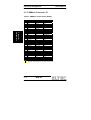
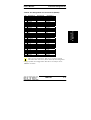
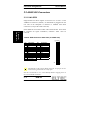
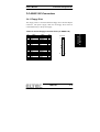
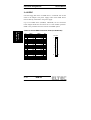
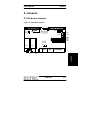
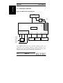
BAB 740
Basic Automation Board with PowerPC 740
manual
Revision 2C
Revision
Revision Changes
Date / Name
1A
First Edition, Valid for Hardware revision 1A
03.01.2000 AR
2A
Valid for Hardware revision 3A
24.04.2001 G.M.
2B
Valid for Hardware revision 3A
Valid for Software revision W-O9B7-106C
26.09.2001 rae
- I/O-Address-Map changed 2C
Disclaimer new
08.11.06 hh
DISCLAIMER
Copyright
© 2006 ELTEC Elektronik AG. The information, data, and figures in this
document including respective references have been verified and
found to be legitimate. In particular in the event of error they may,
therefore, be changed at any time without prior notice. The complete
risk inherent in the utilization of this document or in the results of its
utilization shall be with the user; to this end, ELTEC Elektronik AG shall
not accept any liability. Regardless of the applicability of respective
copyrights, no portion of this document shall be copied, forwarded or
stored in a data reception system or entered into such systems without
the express prior written consent of ELTEC Elektronik AG, regardless of
how such acts are performed and what system is used (electronic,
mechanic, photocopying, recording, etc.). All product and company
names are registered trademarks of the respective companies.
Our General Business, Delivery, Offer, and Payment Terms and
Conditions shall otherwise apply.
Federal communications commission statement
Þ This device complies with FCC Rules Part 15. Operation is subject
to the following two conditions:
Þ This device may not cause harmful interference, and
Þ This device must accept any interference received including
interference that may cause undesired operation.
Þ This equipment has been tested and found to comply with the
limits for a Class B digital device, pursuant to Part 15 of the FCC
Rules. These limits are designed to provide reasonable protection
against harmful interference in a residential installation. This
equipment generates, uses and can radiate radio frequency
energy and, if not installed and used in accordance with
Þ
Þ
Þ
Þ
Þ
manufacturer’s instructions, may cause harmful interference to
radio communications. However, there is no guarantee that
interference will not occur in a particular installation. If this
equipment does cause harmful interference to radio or television
reception, which can be determined by turning the equipment off
and on, the user is encouraged to try correct the interference by
one or more of the following measures:
Reorient or relocate the receiving antenna.
Increase the separation between the equipment and receiver.
Connect the equipment to an outlet on a circuit different from
that to which the receiver is connected.
Consult the dealer or an experienced radio/TV technician for help.
The us of shielded cables for connection of the monitor to the
graphics card is required to assure compliance with FCC
regulations. Changes or modifications to this unit not expressly
approved by the party responsible for compliance could void the
user’s authority to operate this equipment.
Canadian department of communications statement
Þ This digital apparatus does not exceed the Class B limits for radio
noise emissions from digital apparatus set out in the Radio
Interference Regulations of the Canadian Department of
Communications.
Þ This class B digital apparatus complies with Canadian ICES-003
SAFETY INFORMATION
Electrical safety
Þ To prevent electrical shock hazard, disconnect the power cable
from the electrical outlet before reloading the system.
Þ When adding or removing devices to or from the system, ensure
that the power cables for the devices are unplugged before the
signal cables are connected. If possible, disconnect all power
cables from the existing system before you add device.
Þ Before connecting or removing signals cables from motherboard,
ensure that all power cables are unplugged.
Þ Make sure that your power supply is set to the correct voltage in
your area. If you are not sure about the voltage of the electrical
outlet you are using, contact your local power company.
Þ If the power supply is broken, do not try to fix it by yourself.
Contact a qualified service technician or your retailer.
Operation safety
Þ Before installing the motherboard and adding devices on it,
carefully read the manuals that came with the package.
Þ Before using the product, make sure all cables are correctly
connected and the power cables are not damaged. If you detect
any damage, contact your dealer immediately.
Þ To avoid short circuits, keep paper clips, screws, and staples away
from connectors, slots sockets and circuitry.
Þ Avoid dust, humidity, and temperature extremes. Do not place the
product in any area where it may become wet.
Þ Place the product on a stable surface.
Þ If you encounter technical problems with the product, contact a
qualified service technician or your retailer.
EMC Rules
This unit has to be installed in a shielded housing. If not installed in a
properly shielded enclosure, and used in accordance with the
instruction manual, this product may cause radio interference in which
case the user may be required to take adequate measures at his or her
own expense.
IMPROTANT INFORMATION
This product is not an end user product. It was developed and
manufactured for further processing by trained personnel.
RECYCLING
Please recycle packaging environmentally friendly:
Packaging materials are recyclable. Please do not dispose
packaging into domestic waste but recycle it.
Please recycle old or redundant devices environmentally
friendly:
Old devices contain valuable recyclable materials that should
be reutilized. Therefore please dispose old devices at collection points
which are suitable.
User's Manual
Table of Contents
Table of Contents
1 Specification .................................................................... 1—1
1.1 Main Features ............................................................. 1—1
1.2 Specification Details.................................................... 1—2
1.2.1 CPU Kernel .......................................................... 1—2
1.2.2 Flash Memory....................................................... 1—2
1.2.3 PCI Devices.......................................................... 1—2
1.2.4 VMEbus Interface................................................. 1—3
1.2.5 Mechanical ........................................................... 1—3
1.2.6 I/O......................................................................... 1—3
1.2.7 Software ............................................................... 1—4
1.2.8 Compatibility......................................................... 1—4
1.2.9 Related Documents.............................................. 1—4
2 Installation........................................................................ 2—1
2.1 BAB 740 I/O ................................................................ 2—1
2.1.1 VMEbus Installation ............................................. 2—2
2.1.2 What‘s needed for Installation.............................. 2—2
2.1.3 SODIMM Installation ............................................ 2—3
2.1.4 Activity LEDs ........................................................ 2—4
BAB 740
I
Table of Contents
User's Manual
3 Connector Assignments ................................................. 3—1
3.1 On-board Connectors ................................................. 3—1
3.1.1 Keyboard and Mouse Connector ......................... 3—1
3.1.2 Ethernet Connector .............................................. 3—2
3.1.3 Serial Ports 1 and 2 Connectors .......................... 3—2
3.1.4 Parallel I/O Connector.......................................... 3—3
3.1.5 VMEbus Connector P1......................................... 3—4
3.2 ADAP-200 Connectors................................................ 3—6
3.2.1 8-bit SCSI ............................................................. 3—6
3.2.2 Additional I/O........................................................ 3—7
3.3 CONV-300 Connectors ............................................... 3—8
3.4 ADAP-740 Connectors................................................ 3—9
3.4.1 Floppy Disk........................................................... 3—9
3.4.2 EIDE ................................................................... 3—10
3.4.3 COM3 and COM4 .............................................. 3—11
3.4.4 Speaker .............................................................. 3—11
3.5 PMCE-740 Connectors ............................................. 3—12
3.5.1 PMCE-740 VMEbus Connector P1 .................... 3—12
3.5.2 PMCE-740 PCI Mezzanine Card Connectors.... 3—13
II
BAB 740
User's Manual
Table of Contents
3.5.3 PMCE-740 PCI Mezzanine Card I/O Routing .... 3—14
3.5.4 PMCE-740 Power Connector............................. 3—15
4 Board Parameters............................................................ 4—1
4.1 Host Bus...................................................................... 4—1
4.2 VMEbus....................................................................... 4—1
4.3 PCI Local Bus ............................................................. 4—4
4.4 Network ....................................................................... 4—4
4.5 SCSI............................................................................ 4—5
4.6 Serial I/O ..................................................................... 4—5
4.7 Keyboard:.................................................................... 4—5
4.8 Mouse ......................................................................... 4—6
4.9 Parallel I/O .................................................................. 4—6
4.10 MTBF Values ............................................................ 4—6
4.11 ESD Values............................................................... 4—6
4.12 Environmental Conditions ......................................... 4—6
4.13 Maximum Operating Humidity: ................................. 4—7
4.14 Power Requirements ................................................ 4—7
5 Jumpers............................................................................ 5—1
5.1 On-board Jumpers ...................................................... 5—1
BAB 740
III
Table of Contents
User's Manual
5.1.1 User-settable Jumpers ......................................... 5—2
5.2 PMCE-740 Jumpers.................................................... 5—5
5.2.1 PMCE-740 User-settable Jumpers ...................... 5—6
6 Booting ............................................................................. 6—1
6.1 Printout of Boot Screen............................................... 6—1
6.2 Booting OS-9 .............................................................. 6—2
6.2.1 Entering Boot Parameters.................................... 6—2
6.2.2 Printout of Boot Screen ........................................ 6—2
6.2.3 Ethernet Boot Printout.......................................... 6—3
7 Appendix .......................................................................... 7—1
7.1 Description of On-board Devices ................................ 7—1
7.1.1 SMI Ticker ............................................................ 7—1
7.1.2 Enhanced Serial Communications Controller
(ESCC) ................................................................. 7—3
7.1.3 Interrupt Controller ............................................... 7—4
7.1.4 SRAM/RTC........................................................... 7—5
7.1.5 GPIO Use ............................................................. 7—6
7.1.6 Super-I/O Power-on Strappings ........................... 7—6
7.1.7 I/O Address Map .................................................. 7—7
7.1.8 Memory Address Map .......................................... 7—8
IV
BAB 740
User's Manual
Table of Contents
7.1.9 PCI IDSEL ............................................................ 7—9
7.2 Factory-settable Jumpers ........................................... 7—9
BAB 740
V
Table of Contents
User's Manual
List of Tables
Table 1: Activity LEDs .......................................................... 2—4
Table 2: KEYB (6-pin miniature circular connector) ............. 3—1
Table 3: MOUSE (6-pin miniature circular connector) ......... 3—1
Table 4: ETHERNET (8-pin telephone jack connector) ....... 3—2
Table 5: COM1, COM2 (9-pin min-D connector).................. 3—2
Table 6: PRN (25-pin min-D connector) ............................... 3—3
Table 7: VMEbus Connector P1 (X2001) ............................. 3—4
Table 8: Pin Assignment of Connector P2 (X2002) ............. 3—5
Table 9: SCSI Connector 8-bit X103 (on ADAP-200) .......... 3—6
Table 10: 50-Pin I/O Connector X102 (on ADAP-200)......... 3—7
Table 11: COM3, COM4 (9-pin min-D connector)................ 3—8
Table 12: Pinout Floppy Connector X101 (on ADAP-740)... 3—9
Table 13: Pinout EIDE Connector X105 (on ADAP-740) ... 3—10
Table 14: COM3 and COM4 Connectors X103 and X104
(on ADAP-740) ................................................... 3—11
Table 15: Speaker Connector X106 (on ADAP-740) ......... 3—11
Table 16: PMCE-740 VMEbus Connector P1 (X402) ........ 3—12
Table 17: PMCE-740 PCI Mezzanine Card Connectors
(X101, X102, X201, X202). ................................ 3—13
VI
BAB 740
User's Manual
Table of Contents
Table 18: PCI Mezzanine Card Back Plane I/O Routing.... 3—14
Table 19: PMCE-740 Power Connector (X403) ................. 3—15
Table 20: Boot ROM Select (J114) ...................................... 5—2
Table 21: SCSI Termination (J1601) .................................... 5—2
Table 22: SMI Interrupt Routing (J1701) .............................. 5—3
Table 23: Universe PCI Interrupt Routing (J1702...J1705) .. 5—3
Table 24: VMEBus SYSRESET (J1706, J1902) .................. 5—3
Table 25: VMEBus SYSFAIL (J1901) .................................. 5—4
Table 26: COM3 Configuration (J2201, J2202, X2201) ....... 5—4
Table 27: COM4 Configuration (J2203, J2204, X2202) ....... 5—4
Table 28: PMC Slot 1 PCIREQ and PCIGNT Routing ......... 5—6
Table 29: PMC Slot 1 Interrupt Routing ............................... 5—6
Table 30: SMI Status Register read/write............................. 7—2
Table 31: ESCC Address Assignment: ................................ 7—3
Table 32: Interrupt ................................................................ 7—5
Table 33: SRAM/RTC Address Assignment......................... 7—5
Table 34: GPIO Usage ......................................................... 7—6
Table 35: Super-I/O Wake Up Configuration:....................... 7—6
Table 36: I/O Address MAP.................................................. 7—7
BAB 740
VII
Table of Contents
User's Manual
Table 37: Memory Address Map
(default used by VxWorks) ................................... 7—8
Table 38: IDSEL Connection ................................................ 7—9
Table 39: CPU Drive Strength Configuration (J101, J102) .. 7—9
Table 40: CPU PLL Configuration (J103...J106) ................ 7—10
Table 41: System Clock (J111, J112, J113)....................... 7—10
Table 42: MPC106 PLL Configuration (J110...J107) ......... 7—11
Table 43: Cache Size (J601, J602, J603) .......................... 7—11
Table 44: Hardware Debugger Configuration (J1301) ....... 7—12
Table 45: Revision EEPROM Write Protection (J1302) ..... 7—12
VIII
BAB 740
User's Manual
Table of Contents
List of Figures
Figure 1: Block Diagram ....................................................... 1—5
Figure 2: Connection Diagram ............................................. 2—1
Figure 3: Parts Side Jumpers ............................................... 5—1
Figure 4: Solder Side Jumpers ............................................. 5—2
Figure 5: PMCE-740 Jumpers .............................................. 5—5
Figure 6: BAB 740 Interrupt Diagram ................................... 7—4
BAB 740
IX
Table of Contents
X
BAB 740
User's Manual
Specification
Specification
User's Manual
1 Specification
1.1 Main Features
· VMEbus board with two PMC daughter card slots (opt.). Two
VMEbus slots used.
· PowerPC CPU 740 with 266 MHz.
· RAM: 8..256 MB DRAM (2 * 64-bit SO DIMMs)
EDO/SDRAM 50ns.
· Cache: 512kB on-board.
· PCI host bridge: Motorola MPC106.
· PCI-ISA-Bridge: W83C553.
· PCI-to-VME bridge Universe II for fast, global VMEbus
transfers, decoupled from board-internal PCI transfers.
· Flash Eprom: 2 MB onboard, Flash programmable, byte
access implemented in hardware.
· Network interface: Ethernet using DEC21143 (10/100 Mbps)
with PCI-DMA, 10BaseT connector at front panel.
· Serial synchronous (optional): 2 * RS422 / 3 Mb/s
synchronous using Zilog 85230 ESCC.
· Serial asynchronous: 2 * RS232 with PC97307.
· Real-time clock: MK48T59
· SCSI (optional): Symbios 860
· OS-9 operating system with FasTrak cross development
system. - VxWorks operating system with Tornado cross
development system.
· I/O-compatible with BAB-40/60 where applicable.
BAB 740
1—1
Specification
User's Manual
Specification
1.2 Specification Details
1.2.1 CPU Kernel
The CPU kernel consists of the PowerPC-740 CPU with clock rates
of 266 MHz and host bus clocks of 66 MHz. The CPU contains two
parallel 32-bit integer execution units with an additional floating
point unit for 8 SPECint95 and 6.2 SPECfp95 at 200 MHz. It has an
external second-level cache (2-1-1- 1 clocks) and main memory
attached directly to the CPU’s host bus. Memory is controlled by the
host bridge MPC106 which contains the bridge between host bus and
on-board PCI itself as well as the memory interface for EDO or
SDRAM modules in SO DIMM format (144-pin SO DIMM
modules; 64-bit data bus). Memory size can be anywhere between 8
and 128 MB, depending on the DIMM modules used. Two sockets
can be equipped with SO DIMM modules but the board is also
running with only one module.
1.2.2 Flash Memory
Up to 2 MB of user flash memory are supplied for storing usergenerated programs. Thus, diskless systems can be built.
1.2.3 PCI Devices
The board-internal PCI bus is used for all I/O devices as well as the
PCI-to-VME bridge. The PCI bus is of the master/slave type, capable
of DMA transfers as source and target.
Two single-size PMC slots allow for flexible interfacing, e.g. using a
VGA display adapter PMC module and additionally a frame grabber
interface. Due to the bus-master DMA capabilities of the PMC
implementation of the PCI standard, frame grabber can be
implemented efficiently without frame buffers.
1—2
BAB 740
Specification
An Ethernet controller for either 10 Mbps or 100 Mbps Ethernet with
PCI DMA capabilities is provided on-board. Front panel interface is
10/100BaseT.
The last interface on the local PCI bus is the ISA bridge (Winbond
W83C553), interfacing to the internal ISA bus with additional onboard components. Additionally, there are the standard PC
components real-time clock, keyboard controller, dual serial I/O and
parallel controller.
1.2.4 VMEbus Interface
The VMEbus interface uses the Universe II bridge controller,
connecting the internal PCI bus and the external VMEbus. It
supports 8-, 16-, and 32-bit data transfers in master and slave mode.
Additionally, bus controller (arbiter) functionality is available.
Use of the BAB 740 without VMEbus is possible; only power must
be supplied through VME connectors.
1.2.5 Mechanical
The board format is double Eurocard (6HU) using two VMEbus
slots. The VMEbus connectors are mounted at the position of the
second VMEbus slot (the slot on the right) of the two slots the board
is using. Two slots for single-size PMC modules are available.
1.2.6 I/O
8-bit SCSI is routed over the VME P2 connector. Additionally, the
serial I/O channels 2 .... 4 and the parallel I/O are also routed via P2.
On the front panel the Ethernet 10BaseT connector is located as well
as the separate front panel for PMC I/O signals. The keyboard
connector and two serial RS232 channel are also routed to the front
panel (9-pin D connector).
BAB 740
1—3
Specification
User's Manual
Specification
User's Manual
Specification
1.2.7 Software
The standard operating system is OS-9/VxWorks for the PowerPC.
The development environment is FasTrak for Windows, so that the
user can write and debug programs on the Windows 95 or Windows
NT platform. Debug and program download can be done via
Ethernet or through the PCI bus.
BIOS functionality is supplied in the form of the boot program, used
to start the operating system OS-9/VxWorks. It also contains poweron self test routines and PCI device address setup.
1.2.8 Compatibility
The BAB 740 has been designed to be software-compatible to the
PowerPC reference platform (“Yellowknife”) as much as possible.
1.2.9 Related Documents
PowerPC 750 Programmer's Reference: This is the CPU
manufacturer's description of the PowerPC itself and the assembly
language command set.
1—4
BAB 740
Specification
Specification
User's Manual
Figure 1: Block Diagram
PowerPCTM
RISC Microprocessor
(MPC603r, 604r, 740)
68 MHz/64 Bit
Processor Bus
L2 Cache
PCI-/MEM-Controller
(MPC106)
PCI Bus
Memory
(SO-DIMM Sockets)
33 MHz/32 Bit
PCI/PMC
Slot #1
PCI to VME Bridge
(Tundra Universe II)
VMEbus
PCI/PMC
Slot #2
Ethernet Controller
(DEC21143)
Ethernet
Interface
SCSI Controller
(SYM53C860)
SCSI
Interface
IDE
Interface
PCI to ISA Bridge
(W83C553)
ISA Bus
Real Time Clock
(MK48T59)
Enhanced Serial
Comm Controller
(Z85230)
Super I/O Controller
(PC97307)
Serial #3/4
Serial #1/2 Parallel
PS2 Mouse, Keyboard
I2C Bus
Flash EPROM
(512 KB Boot)
(* MB User)
EEPROM
(Config. Info)
BAB 740
1—5
Specification
User's Manual
Specification
1—6
BAB 740
User's Manual
Installation
2 Installation
Installation
2.1 BAB 740 I/O
Figure 2: Connection Diagram
Status/
Control
Keyboard
Mouse
Ethernet
PMC Slot
SCSI
Serial #1
Serial #2
PMC I/O
Serial #3
(syncron)
PMC Slot
Parallel I/O
Serial #4
(syncron)
BAB 740
2—1
Installation
User's Manual
2.1.1 VMEbus Installation
WARNING: Due to the power dissipation of the MPC740
CPU it is not recommended to operate the BAB 740 without
forced air cooling.
Installation
The BAB 740 needs two VMEbus slots, when used with the PMCE
carrier board. Since the two boards (BAB 740 and PMCE) have an
internal connection, be sure to install resp. remove the two-board
package carefully and simultaneously!
2.1.2 What‘s needed for Installation
The BAB 740 must be installed into a 32-bit VMEbus rack. A
terminal (or a PC with a terminal emulator program), set to 9600
baud, 8 bit, no parity, is needed to check boot messages and to
change boot settings. A SCSI hard disk must be attached via an
ADAP-200/220 if the operating system is booted from disk; if it is
booted from Ethernet, this network connection is needed.
2—2
BAB 740
User's Manual
Installation
All 144-pin SO-DIMMs up to 64 MByte and some 128 Mbyte SODIMMs that fit into X701 and X702 can be used with the BAB 740.
The firmware reads the type and size of the SO-DIMM from the SPD
(Serial Presence Detect) EEPROM installed on the memory module.
However there are some restrictions and recommendations:
· SDRAMs should be 100 MHz or faster.
· FPMODE or EDO RAMs should be 60 ns or faster.
· X701 must be populated with a memory module.
· If two memory modules are installed they should be of the
same type but may have different size. Otherwise the
firmware uses only the module installed in X701.
· Due to performance reasons the use of SDRAM is strongly
recommended (50% advantage).
After reset the firmware tests the memory modules. If the test fails or
the firmware reports the wrong size - the module may not be suitable
for the BAB 740.
BAB 740
2—3
Installation
2.1.3 SODIMM Installation
Installation
User's Manual
2.1.4 Activity LEDs
There are four activity LEDs on the front panel of the BAB 740. The
LEDs have a pulse stretcher to make short pulses visible.
Installation
Table 1: Activity LEDs
LED
RUN
DISK
LNK
Color
Green
Yellow
Green/Yellow
ACT
Yellow
2—4
Description
CPU data bus in usage
access to IDE or SCSI bus
green = 100 Mbit link pulses present
yellow = 10 Mbit link pulses present
network activity
BAB 740
User's Manual
Connector Assignments
3 Connector Assignments
Please check the connector assignments before making any
connections!
3.1 On-board Connectors
Connector
Assignments
3.1.1 Keyboard and Mouse Connector
Table 2: KEYB (6-pin miniature circular connector)
Pin
1
2
3
4
5
6
Signal
KBDATA
nc
GND
+5V
KBCLK
nc
Front View
6
5
4
3
2
1
Table 3: MOUSE (6-pin miniature circular connector)
Pin
1
2
3
4
5
6
Signal
MDATA
nc
GND
+5V
MCLK
nc
Front View
6
5
4
3
2
1
BAB 740
3—1
Connector Assignments
User's Manual
3.1.2 Ethernet Connector
Table 4: ETHERNET (8-pin telephone jack connector)
Pin
1
2
3
4
5
6
7
8
1
Signal
TXD+
TXDRXD+
nc
nc
RXDnc
nc
8
Front View
Connector
Assignments
3.1.3 Serial Ports 1 and 2 Connectors
Table 5: COM1, COM2 (9-pin min-D connector)
Pin
1
2
3
4
5
6
7
8
9
3—2
Signal
DCD
RXD
TXD
DTR
GND
DSR
RTS
CTS
RI
Front View
Pin 1
BAB 740
User's Manual
Connector Assignments
3.1.4 Parallel I/O Connector
Table 6: PRN (25-pin min-D connector)
Front View
1
2
3
4
5
6
7
8
9
10
11
12
13
14
15
16
17
18-25
Signal
/STROBE
D1
D2
D3
D4
D5
D6
D7
D8
/ACK
BUSY
PE (Paper End)
SLCT
/AUTO FEED
/ERROR
/INIT
/SLCT IN
GND
Pin 1
Connector
Assignments
Pin
BAB 740
3—3
Connector Assignments
User's Manual
3.1.5 VMEbus Connector P1
Table 7: VMEbus Connector P1 (X2001)
Connector
Assignments
Pin
1
2
3
4
5
6
7
8
9
10
11
12
13
14
15
16
17
18
19
20
21
22
23
24
25
26
27
28
29
30
31
32
Row A
D00
D01
D02
D03
D04
D05
D06
D07
GND
SYSCLK
GND
/DS1
/DS0
/WRITE
GND
/DTACK
GND
/AS
GND
/IACK
/IACKIN
/IACKOUT
AM4
A07
A06
A05
A04
A03
A02
A01
-12 V
+5V
Row B
/BBSY
/BCLR
/ACFAIL
/BG0IN
/BG0OUT
/BG1IN
/BG1OUT
/BG2IN
/BG2OUT
/BG3IN
/BG3OUT
/BR0
/BR1
/BR2
/BR3
AM0
AM1
AM2
AM3
GND
(SERCLK)
(SERDAT)
GND
/IRQ7
/IRQ6
/IRQ5
/IRQ4
/IRQ3
/IRQ2
/IRQ1
+5STDBY
+5V
Row C
D08
D09
D10
D11
D12
D13
D14
D15
GND
/SYSFAIL
/BERR
/SYSRESET
/LWORD
AM5
A23
A22
A21
A20
A19
A18
A17
A16
A15
A14
A13
A12
A11
A10
A09
A08
+12 V
+5V
Signals in parentheses are not connected
3—4
BAB 740
User's Manual
Connector Assignments
Table 8: Pin Assignment of Connector P2 (X2002)
Signal Row A
SPKROUT
SCSIDB0
SCSIDB2
SCSIDB4
SCSIDB6
SCSIDBP0
SCSIDP
IDEDA(0)
IDEDA(1)
IDEDA(2)
IDEDB(13)
/IDEIOCS16
/INDEX
/DR1
/STEP
/WGATE
IDEDB(15)
/SCSIACK
/SCSIMSG
/SCSIC/D
/SCSII/O
C4GND1
C4CTS
C4RTS
C4DCD
C3GND1
C3CTS
C3RTS
C3DCD
/WP
/HDSEL
DRATE0
Signal Row B
+5V
GND
Reserved
A24
A25
A26
A27
A28
A29
A30
A31
GND
+5V
D16
D17
D18
D19
D20
D21
D22
D23
GND
D24
D25
D26
D27
D28
D29
D30
D31
GND
+5V
Signal Row C
SCSIDB1
SCSIDB3
SCSIDB5
SCSIDB7
IDEDB(8)
IDEDB(9)
IDEDB(10)
IDEDB(11)
IDEDB(12)
DENSEL
/DSKCHG
/MTR0
/DR0
/DIR
/SCSIATN
IDEDB(14)
/SCSIBSY
/SCSIRST
/SCSISEL
/SCSIREQ
C4GND4
C4DTR
C4TXD
C4RXD
C3GND4
C3DTR
C3TXD
C3RXD
+5V
/WDATA
/TRK0
/RDATA
Connector
Assignments
Pin
1
2
3
4
5
6
7
8
9
10
11
12
13
14
15
16
17
18
19
20
21
22
23
24
25
26
27
28
29
30
31
32
Lines on rows A and C are TTL-level, except Cx signals
which have RS 232C level (SILC-200 used). Pin assignment
changes for RS 422 configuration. Row B is reserved for 32-bit
VMEbus extension
BAB 740
3—5
Connector Assignments
User's Manual
3.2 ADAP-200 Connectors
3.2.1 8-bit SCSI
Single-ended 8-bit SCSI signals are fed into row A and C of the
VMEbus P2 connector (X2002). An ADAP-200 is plugged onto the
rear side of the backplane to interface to standard 8-bit SCSI
connectors (a 50-pin flat cable connector)
Connector
Assignments
If the BAB 740 is located at either end of the SCSI bus. J1601 must
be installed for signal termination, otherwise J1601 must be
removed.
Table 9: SCSI Connector 8-bit X103 (on ADAP-200)
Front View
1
Pin
2
4
6
8
10
12
14
16
18
20
22
24
26
Description
DB0
DB1
DB2
DB3
DB4
DB5
DB6
DB7
DB8
GND
GND
GND
TERM-PWR
Pin
28
30
32
34
36
38
40
42
44
46
48
50
2
Description
GND
GND
ATN
GND
BSY
ACK
RST
MSG
SEL
CIO
REQ
I/O
49
50
All odd pins of the 50-pin SCSI connector except pin 25 are
connected to ground. Pin 25 is left open.
Pin 26 is connected to +5 V via a Shottky diode to supply power to
an external SCSI terminator.
3—6
BAB 740
User's Manual
Connector Assignments
3.2.2 Additional I/O
Table 10: 50-Pin I/O Connector X102 (on ADAP-200)
Dir
I/O
I
O
O
I
I
O
O
I
-
Description
reserved
Serial Channel 4
Serial Channel 4
Serial Channel 4
Serial Channel 4
Serial Channel 4
Serial Channel 4
Serial Channel 4
not connected
not connected
Serial Channel 3
Serial Channel 3
Serial Channel 3
Serial Channel 3
Serial Channel 3
Serial Channel 3
Serial Channel 3
not connected
not connected
reserved
Remark
GND2
GND1
nc
CTS
TXD
RTS
RXD
GND2
GND1
nc
CTS
TXD
RTS
RXD
Front View
1
2
(may be changed if a
non standard levelconverter board SILC is
installed)
Connector
Assignments
Pin
1..23
24
25
26
27
28
29
30
31
32
33
34
35
36
37
38
39
40
41
42..50
(may be changed if a
non standard levelconverter board SILC is
installed)
49
BAB 740
3—7
50
Connector Assignments
User's Manual
3.3 CONV-300 Connectors
Front View
Pin 1
Table 11: COM3, COM4 (9-pin min-D connector)
Pin
Connector
Assignments
1
2
3
4
5
6
7
8
9
3—8
RS232
async.Signal
(default)
DCD
RXD
TXD
DTR
GND
nc
RTS
CTS
nc
RS232
sync.Signal
DCD
RXD
TXD
DTR
GND
nc
TCLK
RCLK
nc
BAB 740
RS422
async. Signal
CTSRXD+
TXD+
RTSTXDnc
RTS+
CTS+
RXD-
RS422
sync. Signal
RCLKRXD+
TXD+
TCLKTXDnc
TCLK+
RCLK+
RXD-
User's Manual
Connector Assignments
3.4 ADAP-740 Connectors
3.4.1 Floppy Disk
The floppy cable is connected between floppy drive and the adapter
connector. The power supply cable for the floppy drive must be
connected directly to the power supply.
Pin
1
3
5
7
9
11
13
15
17
19
21
23
25
27
29
31
33
Name
Gnd
Gnd
Gnd
Gnd
Gnd
Gnd
Gnd
Gnd
Gnd
Gnd
Gnd
Gnd
Gnd
Gnd
Gnd
Gnd
Gnd
Name
DRVDEN0
nc
DRVDEN1
/INDEX
/MTR0
/DS1
/DS0
MTR1
/DIR
/STEP
/WDATA
/WGATE
/TRK0
/WRTPRT
/RDATA
/HDSEL
/DSKCHG
Pin
2
4
6
8
10
12
14
16
18
20
22
24
26
28
30
32
34
BAB 740
Connector
Assignments
Table 12: Pinout Floppy Connector X101 (on ADAP-740)
Front View
1
2
33
34
3—9
Connector Assignments
User's Manual
3.4.2 EIDE
Like the floppy disk drive an EIDE drive is connected with its flat
cable to the adapter. The power supply cable of the EIDE device
must be directly connected to the power supply.
Up to two EIDE drives (harddisk, CD-ROM) can be connected.
Cable length should not exceed 40 cm to avoid instable operation.
EIDE is only available on board versions with EIDE option.
Table 13: Pinout EIDE Connector X105 (on ADAP-740)
Connector
Assignments
Pin
1
3
5
7
9
11
13
15
17
19
21
23
25
27
29
31
33
35
37
39
3—10
Name
/RST
D7
D6
D5
D4
D3
D2
D1
D0
GND
REQ
/IOW
/IOR
IORDY
/ACK
IRQ14
A1
A0
/CS1
/ACT
Name
GND
D8
D9
D10
D11
D12
D13
D14
D15
nc
GND
GND
GND
nc
GND
nc
nc
A2
/CS3
GND
BAB 740
Pin
2
4
6
8
10
12
14
16
18
20
22
24
26
28
30
32
34
36
38
40
Front View
1
2
39
40
User's Manual
Connector Assignments
3.4.3 COM3 and COM4
Table 14: COM3 and COM4 Connectors X103 and X104
(on ADAP-740)
1
2
3
4
5
6
7
8
9
10
RS232
async.
Signal
(default)
DCD
nc
RXD
RTS
TXD
CTS
DTR
nc (+5V)
GND
nc
RS232
sync.
Signal
RS422
async.
Signal
RS422
sync.
Signal
DCD
nc
RXD
TCLK
TXD
RCLK
DTR
nc (+5V)
GND
nc
CTSnc
RXD+
RTS+
TXD+
CTS+
RTSRXDTXDnc
RCLKnc
RXD+
TCLK+
TXD+
RCLK+
TCLKRXDTXDnc
Front View
1
2
9
10
The pinout of X103 and X104 on ADAP-740 is such that a
crimped cable with a 10 pin edge connector and a 9 pin Min-D
male connector results in the same pinout as Table 11.
3.4.4 Speaker
Table 15: Speaker Connector X106 (on ADAP-740)
Pin
1
2
3
4
+5V
nc
nc
Speaker
Front View
1
4
BAB 740
3—11
Connector
Assignments
Pin
Connector Assignments
User's Manual
3.5 PMCE-740 Connectors
Via the PMC Extension Board (PMCE-740) the BAB 740 can be
expanded by two PMC Modules.
3.5.1 PMCE-740 VMEbus Connector P1
Only GND, +5V and +12V are routed from the VMEbus Connector
P1 to the Power Connector X403. No VMEbus Signals are used.
Connector
Assignments
Table 16: PMCE-740 VMEbus Connector P1 (X402)
Pin
1...8
9
10
11
12..14
15
16
17
18..30
31
32
3—12
Row A
nc
GND
nc
GND
nc
GND
nc
GND
nc
nc
+ 5 V (Cam)
Row C
nc
GND
nc
nc
nc
nc
nc
nc
nc
+ 12 V (Cam)
+ 5 V (Cam)
BAB 740
User's Manual
Connector Assignments
3.5.2 PMCE-740 PCI Mezzanine Card
Connectors
Table 17: PMCE-740 PCI Mezzanine Card Connectors
Jn11, Jn12, Jn21, Jn22 (X101, X102, X201, X202).
X101, X201
Signal Name
Signal Name
TCK
-12V
GND
INTA#
INTB#
INTC#
BUSMODE1#
+5V
INTD#
PCI-RSVD*
GND
PCI-RSVD*
CLK
GND
GND
GNT'
REQ#
+5V
V(I/O)
AD(31)
AD(28)
AD(27)
AD(25)
GND
GND
C/BE(3)#
AD(22)
AD(21)
AD(19)
+5V
V(I/O)
AD(17)
FRAME#
GND
GND
IRDY#
Signal
+5V
GND
LOCK#
SDONE#
SBO#
PAR
GND
V(I/O)
AD(15)
AD(12)
AD(11)
AD(9)
+5V
GND
C/BE(0)#
AD(6)
AD(5)
AD(4)
GND
V(I/O)
AD(3)
AD(2)
AD(1)
AD(0)
+5V
GND
REQ64#
Pin
2
4
6
8
10
12
14
16
18
20
22
24
26
28
30
32
34
36
38
40
42
44
46
48
50
52
54
56
58
60
62
64
Pin
1
3
5
7
9
11
13
15
17
19
21
23
25
27
29
31
33
35
37
39
41
43
45
47
49
51
53
55
57
59
61
63
X102, X202
Signal Name
Signal Name
+12V
TRST#
TMS
TDO
TDI
GND
GND
PCI-RSVD
PCI-RSVD*
PCI-RSVD
BUSMODE2#
+3,3V
RST#
BUSMODE3#
+3,3V
BUSMODE4#
PCI-RSVD
GND
AD(30)
AD(29)
GND
AD(26)
AD(24)
+3,3V
IDSEL
AD(23)
+3,3V
AD(20)
AD(18)
GND
AD(16)
C/BE(2)#
GND
PMC-RSVD
TRDY#
+3,3V
GND
STOP#
PERR#
GND
+3,3V
SERR#
C/BE(1)#
GND
AD(14)
AD(13)
GND
AD(10)
AD(8)
3,3V
AD(7)
PMC-RSVD
+3,3V
PMC-RSVD
PMC-RSVD
GND
PMC-RSVD
PMC-RSVD
GND
PMC-RSVD
ACK64#
+3,3V
GND
PMC-RSVD
BAB 740
3—13
Pin
2
4
6
8
10
12
14
16
18
20
22
24
26
28
30
32
34
36
38
40
42
44
46
48
50
52
54
56
58
60
62
64
Connector
Assignments
Pin
1
3
5
7
9
11
13
15
17
19
21
23
25
27
29
31
33
35
37
39
41
43
45
47
49
51
53
55
57
59
61
63
Connector Assignments
User's Manual
3.5.3 PMCE-740 PCI Mezzanine Card I/O Routing
Table 18 shows the routing of the PMC I/O Connectors to the
VMEbus P2 Connector
Table 18: PCI Mezzanine Card Back Plane I/O Routing
Connector
Assignments
(X203)
Host Jn24
33
34
35
36
37
38
39
40
41
42
43
44
45
46
47
48
49
50
51
52
53
54
55
56
57
58
59
60
61
62
63
64
3—14
(X103)
Host Jn14
1
2
3
4
5
6
7
8
9
10
11
12
13
14
15
16
17
18
19
20
21
22
23
24
25
26
27
28
29
30
31
32
(X401)
VMEbus P2
1C
1A
2C
2A
3C
3A
4C
4A
5C
5A
6C
6A
7C
7A
8C
8A
9C
9A
10C
10A
11C
11A
12C
12A
13C
13A
14C
14A
15C
15A
16C
16A
BAB 740
(X103)
Host Jn14
33
34
35
36
37
38
39
40
41
42
43
44
45
46
47
48
49
50
51
52
53
54
55
56
57
58
59
60
61
62
63
64
(X401)
VMEbus P2
17C
17A
18C
18A
19C
19A
20C
20A
21C
21A
22C
22A
23C
23A
24C
24A
25C
25A
26C
26A
27C
27A
28C
28A
29C
29A
30C
30A
31C
31A
32C
32A
User's Manual
Connector Assignments
3.5.4 PMCE-740 Power Connector
Table 19: PMCE-740 Power Connector (X403)
Description
+5V out
GND
GND
+12V out
Connector
Assignments
Pin
1
2
3
4
BAB 740
3—15
Connector Assignments
Connector
Assignments
3—16
BAB 740
User's Manual
User's Manual
Board Parameters
4 Board Parameters
4.1 Host Bus
66MHz
4.2 VMEbus
VMEbus interface according to specification ANSI/IEEE STD 10141987 (Rev. D1.4)
VMEbus Master/Slave Capabilities:
Board
Parameters
Single cycle:
A16/A24/A32/A64:D08(EO)/D16/D32/UAT
A40:D08(EO)/D16/MD32
RMW (Master only):
A16/A24/A32:D08(EO)/D16/D32
A40:D08(EO)/D16/MD32
BLT: A24/A32/A64:D08(EO)/D16/D32
A40:D08(EO)/D16/MD32
MBLT: A24/A32/A64:D64
ADO: A16/A24/A32/A40/A64/CR/CSR
ADOH: A16/A24/A32/A40/A64
BAB 740
4—1
Board Parameters
User's Manual
System Controller Options:
Arbiter:
BTO(16/32/64), forever
IACK daisy-chain driver
SYSCLK driver
Arbiter Options:
PRI, RRS, SGL
BBSY filter
Requester Options:
Any one of BR(0-3)
RWD, ROR, ROC
Board
Parameters
Bus ownership timer 16 ms... 1024 ms, forever
Interrupt Handler Options:
IH(1-7)
D08(O), D16, D32
Interrupter Options:
I(1-7)
D08(O), D16, D32
Auto Configuration:
FSD, ASI
4—2
BAB 740
User's Manual
Board Parameters
Address Range:
Four PCI target/VME master windows: base and size programmable,
64 KB to 4 GB window size, any of specified address capabilities or
user-defined.
Board
Parameters
Four VME slave/PCI initiator windows: base and size
programmable, 64 KB to 4 GB window size, any of specified
address capabilities or user-defined.
BAB 740
4—3
Board Parameters
User's Manual
4.3 PCI Local Bus
CPU to PCI Transfer Options:
Write post buffer
Max. 120 MB/s (peak)
PCI to Memory Transfer Options:
Max. 120 MB/s (peak)
Clock Speed:
33.3 MHz
IRQs:
Board
Parameters
Four PCI interrupts rerouted to selectable ISA interrupts
4.4 Network
10BaseT/100BaseTx (twisted-pair)
Transfer Speed:
max. 10/100 Mbit/s
4—4
BAB 740
User's Manual
Board Parameters
4.5 SCSI
Ultra SCSI (8 bit)
Transfer Speed:
asynchronous transfer 7 MB/s
synchronous transfer 20 MB/s (ultra SCSI)
4.6 Serial I/O
2 Channels (PC97307):
Full duplex, asynchronous
Board
Parameters
50 b/s - 115,2 KB/s
RS232 level
2 Channels (Z85230 ESCC):
Full duplex
50 b/s - 230,4 KB/s asynchronous
up to 3 MB/s synchronous
RS232 or RS422 level
4.7 Keyboard:
MF2/AT mode
PS/2 mode
BAB 740
4—5
Board Parameters
User's Manual
4.8 Mouse
PS/2 mode
Serial mouse at channel 1 or channel 2
4.9 Parallel I/O
Centronics bidirectional, unbuffered TTL
Transfer Rate: max. 2 MB/s
4.10 MTBF Values
Includes one 64 Mbyte SODIMM:
18900 h (computed after MIL HDBK-217E)
Board
Parameters
253270 h (realistic value from industry stand experience)
4.11 ESD Values
2 kV (Human body method)
4.12 Environmental Conditions
Storage Temperature: -40° C - +70° C (non condensing)
Operating Temperature: 0° C - +50° C (1 m/s forced air cooling)
4—6
BAB 740
User's Manual
Board Parameters
4.13 Maximum Operating Humidity:
85% relative
4.14 Power Requirements
Total Power Requirements (without PCI extensions)
3,8 A max. 3.0 A typ. +5 VDC +/-5%
100 mA max. 30 mA typ. +12 VDC +/-10%
100 mA max. 10 mA typ. -12 VDC +/-10%
Battery
Board
Parameters
Type M4T28-BR12SH1
Approx. 8 years life time
BAB 740
4—7
Board Parameters
Board
Parameters
4—8
BAB 740
User's Manual
User's Manual
Jumpers
5 Jumpers
5.1 On-board Jumpers
Figure 3: Parts Side Jumpers
X2001
J1706
J1301
J1705
J1704
J1703
J1702
J1701
X1301
X2201
X2202
J2203
J2201
J2204
J2202
X201
X202
X203
X204
X205
J1201
J114
J1302
J1601
J1901
J1902
X2001
S1201
S1001
X701
X2101
X1101
X1104
X1105
X1103
X1102
Jumpers
X702
BAB 740
5—1
Jumpers
User's Manual
J107
J108
J109
J110
J111
J112
J113
J103
J104
J105
J106
J602
J601
J603
J102
J101
Figure 4: Solder Side Jumpers
5.1.1 User-settable Jumpers
Table 20: Boot ROM Select (J114)
J114
open
Short
Description
Boot from Boot-ROM
Boot from User-ROM (default)
Jumpers
Table 21: SCSI Termination (J1601)
J1601
Open
short
5—2
Operation
disable termination
enable termination (default)
BAB 740
User's Manual
Jumpers
Table 22: SMI Interrupt Routing (J1701)
J1701
1-3
2-4
4-6
3-5
7-8
Function
no SMI interrupt
route Universe INT0 to SMI
route Universe INT0 to SMI
route Universe INT0 to SMI
route Universe INT0 to SMI
route SMITICK to SMI (default)
J1702
1-2
2-3
Function
no Universe INT0, INT1 on PCI
route Universe INT0 to PCI IRQ A
route Universe INT1 to PCI IRQ A
J1703
1-2
2-3
Function
no Universe INT2, INT3 on PCI
route Universe INT2 to PCI IRQ B
route Universe INT3 to PCI IRQ B
J1704
1-2
2-3
Function
no Universe INT4, INT5 on PCI
route Universe INT4 to PCI IRQ C
route Universe INT5 to PCI IRQ C
J1705
1-2
2-3
Function
no Universe INT6, INT7 on PCI
route Universe INT6 to PCI IRQ D
route Universe INT7 to PCI IRQ D (default)
Jumpers
Table 23: Universe PCI Interrupt Routing (J1702...J1705)
Table 24: VMEBus SYSRESET (J1706, J1902)
J1706
short
Short
J1902
short
Short
Function
no VMEbus SYSRESET
VMEbus SYSRESET is input
VMEbus SYSRESET is output (default)
not allowed
BAB 740
5—3
Jumpers
User's Manual
Table 25: VMEBus SYSFAIL (J1901)
J1901
Open
short
Function
no VMEbus SYSFAIL
VMEbus SYSFAIL output enable (default)
Table 26: COM3 Configuration (J2201, J2202, X2201)
J2201
1-2
3-5
6-8
2-4
6-8
6-8
4-6
J2202
1-2
5-6
1-2
4-6
1-2
2-4
X2201
SILC-200
Configuration
RS232 async.
(default)
SILC-200
RS232 sync.
SILC-300
SILC-300
RS422 async.
RS422 sync.
Table 27: COM4 Configuration (J2203, J2204, X2202)
J2203
1-2
3-5
6-8
2-4
6-8
6-8
4-6
J2204
1-2
5-6
1-2
4-6
1-2
2-4
X2202
SILC-200
Configuration
RS232 async.
(default)
SILC-200
RS232 sync.
SILC-300
SILC-300
RS422 async.
RS422 sync.
Jumpers
5—4
BAB 740
User's Manual
Jumpers
5.2 PMCE-740 Jumpers
R101
R102
R103
R104
X402
X102
J201
J202
J204
Figure 5: PMCE-740 Jumpers
X103
X101
X401
X202
X203
X201
SLOT 0
SLOT 1
Jumpers
X403
BAB 740
5—5
Jumpers
User's Manual
5.2.1 PMCE-740 User-settable Jumpers
Table 28: PMC Slot 1 PCIREQ and PCIGNT Routing
J201
1-2
3-4
J202
1-2
3-4
Description
Use PCIREQ, PCIGNT of PMC Slot 0
Use PCIREQ, PCIGNT of BAB 740 Onboard SCSI Controller
Warning: PCIREQ and PCIGNT of PMC Slot 0 or SCSI
Controller can only be used, if the corresponding device is
not equipped!
Table 29: PMC Slot 1 Interrupt Routing
J204
1-2
3-4
5-6
7-8
Description
Route PMC IRQ A to PCI IRQ A
Route PMC IRQ A to PCI IRQ B
Route PMC IRQ A to PCI IRQ C
Route PMC IRQ A to PCI IRQ D
Jumpers
5—6
BAB 740
User's Manual
Booting
6 Booting
6.1 Printout of Boot Screen
This chapter shows how the terminal screen looks like on a BAB 740
after power-on.
*** ELTEC Elektronik, Mainz ***
BAB-PPC Monitor Version 1.2/2
Init MPU/MSR/FPU/Segment registers.
Init SuperIO (polled output on COM1).
Activating 1st level cache .................... OK
Setting MPC106 register ....................... OK
Reading SPD of bank0/1 ........................ OK
RAM-Type: SDRAM
Reading SPD of bank2/3 .................... FAILED
Activating 64 MByte.
PowerPC 74x/75x Ver.0008 Rev.3202 at 292 / 83 MHz
PCI devices on local bus ...
No. VendorId DeviceId Device Class
Sub-Class
__________________________________________________
00 1057
0002
Bridge device
00
0B 10AD
0565
Bridge device
01
0D 1000
000F
Mass storage controller 00
0E 1011
0019
Network controller
00
13 1011
0024
Bridge device
04
Press any key to skip memory test :
65536 KByte
Booting
After this screen output, the standard VxWorks monitor will be
started. To modify boot parameter follow the instructions provided
by VxWorks development documentation.
BAB 740
6—1
Booting
User's Manual
6.2 Booting OS-9
6.2.1 Entering Boot Parameters
The BAB 740 is prepared for booting over Ethernet using BOOTP
protocol.
6.2.2 Printout of Boot Screen
*** ELTEC Elektronik GmbH, Mainz ***
BAB 740 Monitor Version 1.0/1
Init MPU/MSR/FPU/Segment registers.
Init SuperIO (polled output on COM1).
Activating 1st level cache --------------------------Setting MPC106 register -----------------------------Reading SPD of bank0/1 ------------------------------RAM-Type: SDRAM
Reading SPD of bank2/3 ------------------------------Activating 32 MByte.
OK
OK
OK
FAILED
OS-9000 Bootstrap for the PowerPC(tm)
Ethernet 10 Mbit selected
BOOTING PROCEDURES AVAILABLE -----------------------<INPUT>
Boot loaded system in-place (copy User-ROM to RAM) -<bo>
Boot over Ethernet (DEC 21143) ---------------------<eb>
Scan SCSI devices ----------------------------------<ioi>
PCI View Utility -----------------------------------<pciv>
Enter ROM Debugger ---------------------------------<break>
Restart the System ---------------------------------<q>
Select a boot method from the above menu:
(Booting procedure up to boot menu may take about half a minute in
this release.)
Booting
6—2
BAB 740
User's Manual
Booting
6.2.3 Ethernet Boot Printout
If a BOOTP server is available in the local network and the BAB
740 is known by this server, the BAB 740 will boot over Ethernet
after entering ‚eb‘ at the boot menu prompt.
Note: The BOOTP server must send the response directly to the BAB
740. Broadcasts will not be analyzed by the BAB 740 in this case.
Select a boot method from the above menu: eb
Bootp: sending bootp request for Address 00:00:5b:00:37:39
Bootp: Got Response from server: c2.00.00.38
My IP Address will be: c2.00.00.b8
My Bootfile is: /tftpboot/B740/os9boot
Bootp: My bootfile size is: 00000cc3 (512-byte) blocks
My subnet mask is: ff.ff.ff.00 <<no timeoffset tag>>
Tftp: Sending tftp Request...
................................................................
o
o
o
.................................................................
.................................................................
Tftp: received file with 0019840c bytes
Bootfile received from server c2.00.00.38
Now searching for an OS-9000 Kernel...
A valid OS-9000 bootfile was found.
[1]$
Booting
After the boot file is transferred, OS-9 is booting.
BAB 740
6—3
Booting
User's Manual
Booting
6—4
BAB 740
Appendix
Appendix
User's Manual
7 Appendix
7.1 Description of On-board Devices
This chapter describes how the on-board devices are accessed by
operating system drivers. When an operating system, such as OS-9
and VxWorks, is used, there should be no need to address these
devices with user-written code.
7.1.1 SMI Ticker
The output of counter/timer 2 of the W83C553F may be routed to the
System Management Interrupt input of the CPU when J1701 is set to
position 7-8. This can be used to generate a periodic interrupt with
higher priority than normal interrupts. A negative edge of the PCSpeaker output triggers the SMI when enabled via bit 7 of I/O
address $809.
Writing to I/O address $808 clears the SMI.
BAB 740
7—1
Appendix
User's Manual
Appendix
Table 30: SMI Status Register read/write
Register
SMI Status register
D7
SMIPE
D6
D5
D4
D3
D2
D1
D0
Read:
SMISR: I/O Address: $808
SMIPE = 0: no SMI pending
SMIPE = 1: SMI pending
Write:
Clears pending SMI
Register
SMI Status register
D7
SMIPE
D6
Write:
SMICR: I/O Address: $809
ENSMI = 0: disable SMI
ENSMI = 1: enable SMI
7—2
BAB 740
D5
D4
D3
D2
D1
D0
Appendix
Appendix
User's Manual
7.1.2 Enhanced Serial Communications
Controller (ESCC)
In addition to the two serial controllers COM1 and COM2 that are
incorporated in the PC97307 Super-I/O the BAB 740 features
another two serial lines that are realized with a Z85230 ESCC. The
ESCC is clocked with 12 MHz or 14.7456 MHz. This allows transfer
rates up to 3 MBaud synchronous and 230.4 KBaud asynchronous.
Channel A can be operated with DMA to reduce interrupt load of the
CPU for synchronous block protocols. DMA channel 0 is used for
receive and Channel 1 for transmit. The DMA controller must be
programmed to type A or B mode. The Interrupt request of the
ESCC is connected to INT9 input of the interrupt controller.
Table 31: ESCC Address Assignment:
I/O Address
$800
$801
$802
$803
Description
ESCC Channel B Control
ESCC Channel A Control
ESCC Channel B Data
ESCC Channel A Data
BAB 740
7—3
Appendix
User's Manual
Appendix
7.1.3 Interrupt Controller
Figure 6: BAB 740 Interrupt Diagram
PowerPC
INT
SMI
VME
Timer #2
INT OUT
Timer #1
INT 0
Timer #0
IDE #1
W83C553
IDE #0
PCI
INT A INT B INT C INT D
INT 9
INT 5
INT 1; 3..12; 14; 15
...........
PMC #1
ESCC
(Z85230)
PMC #2
RTC
(MK48T59)
Super I/O
(PC97307)
SCSI
Network
VME
This diagram shows how the on-board interrupt sources are
connected to the interrupt controller, located logically in the
W83C553 chip. This chip then prioritizes and drives the two CPU
interrupt inputs. The priority scheme used is shown below:
7—4
BAB 740
User's Manual
Appendix
Priority
1
2
3
4
5
6
7
8
9
10
11
12
13
14
15
ISA IRQ
INT 0
INT 1
INT 8
INT 9
INT10
INT 11
INT 12
INT 13
INT 14
INT 15
INT 3
INT 4
INT 5
INT 6
INT 7
PCI IRQ
INT A
INT B
INT C
INT D
Appendix
Table 32: Interrupt
Source
Timer 0 (Ticker)
Keyboard
ESCC
PMC #1
SCSI or PMC #2
Ethernet
VME
Serial #2
Serial #1
RTC
Floppy
Parallel Port
7.1.4 SRAM/RTC
A indirect addressing scheme is used to access the M48T59Y
SRAM/RTC. To access the SRAM/RTC the desired address first
must be written to I/O address $70 and $71. Then the data can be
accessed via I/O address $76. The interrupt output of the M48T59Y
is connected with the INT5 input of the interrupt controller. It may
be used to generate periodic interrupts or watchdog interrupts.
Table 33: SRAM/RTC Address Assignment
I/O Address
$070
$071
$076
Description
SRAM/RTC LSB Address
SRAM/RTC MSB Address
SRAM/RTC Data
BAB 740
7—5
Appendix
User's Manual
Appendix
7.1.5 GPIO Use
The GPIOs of the Super-I/O are used for the following purposes:
Table 34: GPIO Usage
Name
GPIO10
GPIO11
GPIO12
GPIO13
GPIO14
GPIO15
GPIO16
GPIO17
Type
I
I
I/O
O
I/O
O
-
GPIO20
GPIO21
GPIO22
GPIO23
GPIO24
GPIO25
GPIO26
GPIO27
I
I
I
I
Function
not used
CPU Bus Speed (0 = 83 MHz; 1 = 66MHz)
L2 Cache Size (0 = 256 KByte; 1 = 512KByte)
I2C Data for SPD of 2nd SODIMM
I2C Clock for SPD of 2nd SODIMM
I2C Data for SPD of 1st SODIMM, ELTEC Revision EEPROM
I2C Clock for SPD of 1st SODIMM, ELTEC Revision EEPROM
not used
not used
not used
not used
not used
HEX Switch LSB
HEX Switch
HEX Switch
HEX Switch MSB
7.1.6 Super-I/O Power-on Strappings
The Super-I/O wakes up in the following configuration:
Table 35: Super-I/O Wake Up Configuration:
Pin
CFG0
CFG1
CFG3,2
BADDR1,0
SELCS
7—6
Configuration
FDC, KBC and RTC inactive
No X-Bus Data Buffer
Clock source is 24 MHz fed via X1 Pin
PnP Motherboard, Wake in Config state, Index 015Ch
/CS0 on /CS0 pin
BAB 740
Appendix
7.1.7 I/O Address Map
After initialization the following I/O address map becomes effective:
Table 36: I/O Address Map
I/O Address
$000-$00F
$020-$021
$040-$043
$060
$061
$064
$070
$071
$076
$078-$07B
$081-$082
$087
$089-$08B
$092
$0A0-$0A1
$0C0-$0DE
$15C
$15D
$220-$223
$224-$227
$278-$27F
$2F8-$2FF
$3F0-$3F7
$3F8-$3FF
$3C2-$3C9
$3CE-$3CF
$3D4-$3D5
$4D0-$4D1
$808
$809
$800
$801
$802
$803
Device
W83C553F
W83C553F
W83C553F
PC97307
W83C553F
PC97307
M48T59Y
M48T59Y
M48T59Y
W83C553F
W83C553F
W83C553F
W83C553F
W83C553F
W83C553F
W83C553F
PC97307
PC97307
PC97307
PC97307
PC97307
PC97307
PC97307
PC97307
SM810
SM810
SM810
W83C553F
MACH210
MACH210
Z85230
Z85230
Z85230
Z85230
Description
DMA Controller 1
Interrupt Controller 1
Counter/Timer
Keyboard Data
Port B
Keyboard Control
SRAM/RTC LSB Address
SRAM/RTC MSB Address
SRAM/RTC Data
BIOS Timer
DMA Page
DMA Page
DMA Page
Port 92
Interrupt Controller 2
DMA Controller 2
SuperI/O Index
SuperI/O Data
GPIO Port 1
GPIO Port 2
Parallel Port
COM2
Floppy
COM1
VGA Controller
VGA Controller
VGA Controller
Interrupt Mode
SMI Status Register
SMI Control Register
ESCC Channel B Control
ESCC Channel A Control
ESCC Channel B Data
ESCC Channel A Data
BAB 740
7—7
Appendix
User's Manual
Appendix
User's Manual
Appendix
7.1.8 Memory Address Map
The BAB 740 uses address map B (CHRP) of the MPC106. After
initialization the following address map becomes effective:
Table 37: Memory Address Map
(default used by VxWorks)
CPU Address
$0000.0000-$07FF.FFFF
$0800.0000-$7FFF.FFFF
$8000.0000-$F9FF.FFFF
$FA00.0000-$FAFF.FFFF
$F903.0000-$F903.EFFF
$F904.0000-$F904.FFFF
PCI Address
$8000.0000-$F9FF.FFFF
$FA00.0000-$FAFF.FFFF
$F903.0000-$F903.EFFF
$F904.0000-$F904.FFFF
$FB00.0000-$FCFF.FFFF
$FD00.0000-$FDFF.FFFF
$FE00.0000-$FE00.FFFF
$FE01.0000-$FE7F.FFFF
$FE80.0000-$FE80.FFFF
$FE81.0000-$FE81.FFFF
$FB00.0000-$FCFF.FFFF
$0000.0000-$00FF.FFFF
$0000.0000-$0000.FFFF
$0080.0000-$0080.FFFF
$0081.0000-$0081.FFFF
$FE82.0000-$FE82.FFFF
$0082.0000-$0082.FFFF
$FE83.0000-$FEBF.FFFF
$FEC0.0000-$FEDF.FFFF
$0083.0000-$00BF.FFFF
CONFIG_ADDR
$FEE0.0000-$FEEF.FFFF
CONFIG_DATA
$FEF0.0000-$FEFF.FFFF
$FF00.0000-$FF7F.FFFF
J114 open:
$FF80.0000-$FF9F.FFFF
$FFA0.0000-$FFBF.FFFF
$FFC0.0000-$FFC7.FFFF
$FFC8.0000-$FFFF.FFFF
J114 closed:
$FF80.0000-$FF87.FFFF
$FF88.0000-$FFBF.FFFF
$FFC0.0000-$FFDF.FFFF
$FFE0.0000-$FFEF.FFFF
$FFF0.0000-$FFFF.FFFF
$FEF0.0000-$FEFF.FFFF
-
Device
local RAM
reserved
PCI memory space
PCI memory space (PMVIEW)
PCI memory space (PMGRAB)
PCI memory space
(UniverseII)
PCI memory space (VMEbus)
PCI/ISA memory space
PCI/ISA I/O space
reserved
PCI I/O space
PCI I/O space (SCSI
Controller)
PCI I/O space (LAN
Controller)
PCI I/O space
PCI configuration address
register
PCI configuration data
register
PCI interrupt acknowledge
reserved
$FF80.0000-$FF9F.FFFF
$FFA0.0000-$FFBF.FFFF
$FFC0.0000-$FFC7.FFFF
$FFC8.0000-$FFFF.FFFF
User Flash EPROM
Mirrored User Flash EPROM
System Flash EPROM
Mirrored System Flash EPROM
$FF80.0000-$FF87.FFFF
$FF88.0000-$FFBF.FFFF
$FFC0.0000-$FFDF.FFFF
$FFE0.0000-$FFEF.FFFF
$FFF0.0000-$FFFF.FFFF
System Flash EPROM
Mirrored System Flash EPROM
User Flash EPROM
2nd MByte User Flash EPROM
2nd MByte User Flash EPROM
7—8
BAB 740
Appendix
7.1.9 PCI IDSEL
The IDSEL input of each PCI device is connected to one of the PCI
address/data lines for individual addressing in configuration space.
Table XX shows the connection of the IDSEL signal for the various
devices on the BAB 740 and the PMC carrier board.
Table 38: IDSEL Connection
Device
Number
0
11
13
14
15
16
30
IDSEL
AD(11)
AD(13)
AD(14)
AD(15)
AD(16)
AD(30)
Device
MPC106
W83C553F
SYM53C860
21143
PMC Slot 0
PMC Slot 1
Universe II
Note that the device numbers differ from Intel convention where
number 0 corresponds to AD(11) and number 20 corresponds to
AD(31). Configuration cycles with device number 0 are handled
internally in the MPC106 and therefore don‘t correspond with a
address/data line.
7.2 Factory-settable Jumpers
Table 39: CPU Drive Strength Configuration (J101, J102)
J102
short
short
-
J101
short
short
-
Description
disabled
normal (default)
strong
herculean
SMD jumper for factory use only
Note: Implementation specific settings; do not change!
BAB 740
7—9
Appendix
User's Manual
Appendix
User's Manual
Appendix
Table 40: CPU PLL Configuration (J103...J106)
J106
short
short
short
short
short
short
short
short
-
J105
short
short
short
short
short
short
short
short
-
J104
short
short
short
short
short
short
short
short
-
J103
short
short
short
short
short
short
short
short
-
Bus Mult.
x7
bypass
x2
x 6,5
x 2,5
x 4,5
x3
x 5,5
x4
x5
x6
x 3,5
off
Bus Clock
25-33
60-83
25-40
50-83
33-60
40-83
25-40
33-66 (default)
25-50
25-40
40-75
off
SMD jumper for factory use only
Note: Implementation specific settings; do not change!
Table 41: System Clock (J111, J112, J113)
J111
short
short
short
short
J112
short
short
J113
short
short
short
short
short
CPU Bus Clock
30
60
62,5
66
75
83
PCI Bus Clock
25
30
25
33 (default)
37,5
33
SMD jumper for factory use only!
Note: Implementation specific settings; do not change!
7—10
BAB 740
User's Manual
Appendix
J110
short
short
short
short
short
short
short
short
-
J109
short
short
short
short
short
short
short
short
-
J108
short
short
short
short
short
short
short
short
-
J107
short
short
short
short
short
short
short
short
-
Mult.
x1
x1
bypass
x2
x2
x 2,5
x 2,5
x3
x3
off
Bus Clock
33
16-25
66
33-50
83
41-50
75-100
50
-
Appendix
Table 42: MPC106 PLL Configuration (J110...J107)
PCI Clock
33
16-25
33 (default)
16-25
33
16-20
25-33
16
-
SMD jumper for factory use only
Note: Implementation specific settings; do not change!
Table 43: Cache Size (J601, J602, J603)
J601
1-2
2-3
J602
1-2
2-3
J603
open
short
PCI Bus Clock
512 Cache (default)
256 Cache
SMD jumper for factory use only!
Note: Implementation specific settings; do not change!
BAB 740
7—11
Appendix
User's Manual
Appendix
Table 44: Hardware Debugger Configuration (J1301)
J1301
1-2
2-3
Operation
normal operation (default)
enable COP
Note: Implementation specific settings; do not change!
Table 45: Revision EEPROM Write Protection (J1302)
J1302
open
short
7—12
Operation
write protect
write enable (default)
BAB 740
BAB 740 Revision
BAB 740 version:
Memory size:
Hardware revision:
Serial number:
BSP revision:
System monitor revision:
BAB 740 Configuration
BAB 740 IP address:
Host IP address:
User name:
Ftp password:
Boot file:
Boot configuration (ftp, bootp, ...)
Host Configuration
Ethernet IP address:
Development tool revision
(VxWorks, OS-9, ...)
Operating system and revision
(WinNT, ...)
Error Description
What must be done to reproduce the error:
Editional configuration (VxWorks: config.h)
Send the completed form to:
ELTEC Elektronik AG
Support, Mainz/Germany
Phone:
+49 (6131) 918-500
Fax:
+49 (6131) 918-196
E-Mail:
[email protected]
Web:
http://www.eltec.com
NOTES: