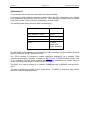
1
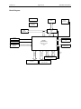
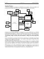
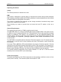
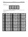
SMT395E User Manual User Manual (QCF42); Version 3.0, 5/2/01; © Sundance Multiprocessor Technology Ltd. 2001 Version 2.1 Page 2 of 30 SMT395Q User Manual Revision History Date Comments Engineer Version 02/11/2005 First rev, based on 395Q AL 1.0 08/04/2006 Added: Power connector SM 2.0 06/06/2006 Minor corrections SM 2.1 Version 2.1 Page 3 of 30 SMT395Q User Manual Table of Contents Revision History ....................................................................................................... 2 Contacting Sundance............................................................................................... 4 Notational Conventions ........................................................................................... 5 C60 ......................................................................................................................... 5 Register Descriptions .............................................................................................. 5 Outline Description .................................................................................................. 6 Block Diagram .......................................................................................................... 7 Architecture Description.......................................................................................... 8 TMS320C6416T ......................................................................................................... 9 Boot Mode............................................................................................................. 10 Flash Boot........................................................................................................ 10 EMIF Control Registers......................................................................................... 11 SDRAM .................................................................................................................... 12 FLASH ..................................................................................................................... 12 FLASH Paging ................................................................................................. 12 Virtex-II Pro FPGA .................................................................................................. 13 External Clock......................................................................................................... 13 Version control ....................................................................................................... 13 Reprogramming the firmware and boot code ...................................................... 13 FPGA resources ..................................................................................................... 14 Interrupts............................................................................................................... 14 Communication ports ............................................................................................ 14 SDB ...................................................................................................................... 14 SDB Clock selection .......................................................................................... 14 RSL ....................................................................................................................... 14 Global bus............................................................................................................. 14 CONFIG & NMI ..................................................................................................... 14 Timer..................................................................................................................... 14 IIOF interrupt......................................................................................................... 15 LED ....................................................................................................................... 15 TTL ....................................................................................................................... 15 Version 2.1 Page 4 of 30 SMT395Q User Manual System Control ....................................................................................................... 16 Board Operating Parameters ................................................................................ 19 Code Composer Studio.......................................................................................... 22 3L Diamond DSP..................................................................................................... 22 Operating Conditions ............................................................................................. 23 Safety.................................................................................................................... 23 EMC ...................................................................................................................... 23 General Requirements .......................................................................................... 23 Power Consumption.............................................................................................. 23 PCB description...................................................................................................... 24 Component Side ................................................................................................... 24 Solder Side ........................................................................................................... 25 Power Connector.................................................................................................... 26 Jumpers/Links ........................................................................................................ 26 JP3 – Prog Sel. ..................................................................................................... 26 JP1 – FPGA JTAG ................................................................................................ 26 JP2- TTL I/O ......................................................................................................... 27 SHB pin-out........................................................................................................... 27 RSL pin-out ........................................................................................................... 28 Virtex Memory Map................................................................................................. 29 FPGA Pin-Out.......................................................................................................... 30 Bibliography............................................................................................................ 30 Contacting Sundance You can contact Sundance for additional information by logging onto the support forum. Version 2.1 Page 5 of 30 SMT395Q User Manual Notational Conventions C60 The terms C60, C64xx and TMS320C64xx will be used interchangeably throughout this document. Register Descriptions The format of registers is described using diagrams of the following form: 31–24 23–16 15–8 7–0 R,00000000 R,10000000 LEVEL R,00000000 RW,10000000 The digits at the top of the diagram indicate bit positions within the register and the central section names bits or bit fields. The bottom row describes what may be done to the field and its value after reset. Shaded fields are reserved and should only ever be written with zeroes. R Readable by the CPU W Writeable by the CPU RW Readable and writeable by the CPU Binary digits indicate the value of the field after reset. Version 2.1 Page 6 of 30 SMT395Q User Manual Outline Description The SMT395E is Sundance’s 4th generation of Texas Instruments ‘C6x DSP TIM (Texas Instruments Module). This module uses one TMS320C6416T DSP which have clock speeds of up to 1GHz. The module also includes a Xilinx Virtex-II/Pro (XC2VP70FF1704) FPGA which is configured to provide ‘C4x style ComPorts, a TIM compatible enhanced Global bus, two Sundance High-Speed Busses (SHBs), 14 Sundance RSL, and other control functions. The SMT395E is, from the user’s perspective, a single-DSP version of the SMT395Q Module. The SMT395E is supported by the TI Code Composer Studio, 3L Diamond DSP and 3L Diamond FPGA to enable full Multi-processor systems with minimum efforts by the programmers. The SMT395E is a C64xx-based size 2 TIM offering the following features: One TMS320C6416T processors running at 1GHz Four 20MB/s communication ports (ComPorts) 128MB of SDRAM (120MHz) 8MBytes of Flash ROM for boot code and FPGA programming Global expansion connector High bandwidth data I/O via 2 Sundance High-speed Buses (SHB). Fourteen 2.5Gbit/sec Rocket Serial Links (RSL) for InterModule communications Power and temperature monitoring Version 2.1 Page 7 of 30 SMT395Q User Manual Block Diagram Oscillators Flash (CE1) 64Mbit Power monitoring voltage convertors 1.5V & 1.2V EMIFA A 'C6416T DSP 16 bit 64 bit DRAM 128MBytes HPI Serial port 14 LEDs & 4 I/O pins J3 Global Expansion Connector 256MBytes DDR memory Timer & Control 2x Comm-Ports 24 I/O pins 2x Comm-Ports 24 I/O pins VirtexII-Pro, FF1704 996 I/O Pins 1.5V 120 I/O Pins; 16-bit Data Global Bus 74 I/O pins Sundance HighSpeed Bus 60-way x2 Sundance RSL x14 FPGA (XC2VP70) JTAG Header J1 Top Primary TIM Connector Comm-Port 0 & 3 J2 Bottom Primary TIM Connector Comm-Port 1 & 4 JTAG chain Version 2.1 Page 8 of 30 SMT395Q User Manual Architecture Description The SMT395E TIM consists of a Texas Instruments TMS320C6416T running at up to 1GHz. Modules are populated with 128MBytes of SDRAM for the DSP, and 256MBytes of DDRSDRAM for the FPGA. A Field Programmable Gate Array (FPGA) is used to manage Global bus accesses and implement four ComPorts, and two Sundance High Speed Buses. This is a Xilinx VirtexII/Pro device. Version 2.1 Page 9 of 30 SMT395Q User Manual TMS320C6416T The processor will run with zero wait states from internal SRAM. An on-board crystal oscillator provides the clock used for the C60. Alternatively, an on-board clock synthesiser provides the clock for the C60. The synthesiser frequency can be altered under DSP control. These clocks are multiplied by 20 by the DSP. The following table shows the main DSP characteristics. Feature C6416T DMA / McBSP / Timer 64/3/3 On-chip memory 1056k bytes Speed 1GHz Others UTOPIA Viterbi and Turbo decoders The SMT395E implementation using this DSP provides interfaces using the EMIFs (External Memory Interfaces A & B), timers and JTAG. The JTAG interface is provided to enable application debugging via a suitable JTAG controller and software. Typically, this will be a SMT310 and TI Code Composer Studio. This is an invaluable interface which enables the application programmer to quickly debug a ‘chain’ of processors in single or multi-processor situations. The EMIF_A is used to connect to a 120MHz, 128MBytes bank of SDRAM, and the VirtexII/Pro. The flash is connected via EMIF_B as a 16-bit device. The EMIF_A supplies 4 ‘chip selects’ which are used for these selections. Version 2.1 Page 10 of 30 SMT395Q User Manual Boot Mode The SMT395E is configured to boot from flash after a reset. Flash Boot 1. The processor copies a bootstrap program from the first part of the flash memory into internal program RAM starting at address 0. 2. Execution starts at address 0. The standard bootstrap supplied with the SMT395E then performs the following operations: 1. All relevant C60 internal registers are set to default values; 2. The FPGA is configured from data held in flash memory and sets up the ComPorts, the Global bus and the Sundance High-speed Buses. This step must have been completed before data can be sent to the ComPorts from external sources such as the host or other TIMs; 3. A C4x-style boot loader is executed. This will continually examine the four ComPorts until data appears on one of them. The bootstrap will then load a program in boot format from that port; the loader will not read data arriving on other ports. See “Application Development” for details of the boot loader format; 4. Finally, control is passed to the loaded program. The delay between the release of the board reset and the FPGA configuration is around 2s for a SMT395E. A typical time to wait after releasing the board reset should be in excess of this delay, but no damage will result if any of the I/Os are used before they are fully configured. In fact, the ComPorts will just produce a not ready signal when data is attempted to be transferred during this time, and then continue normally after the FPGA is configured. Version 2.1 Page 11 of 30 SMT395Q User Manual EMIF Control Registers The C6416 has two external memory interfaces (EMIFs). EMIF_A is 64 bits wide, the EMIF_B is 16 bits wide. The C60 contains several registers that control the external memory interfaces (EMIFs). A full description of these registers can be found in the C6000 Peripherals Reference Guide. The standard bootstrap will initialise these registers to use the following resources: Memory space Resource Address range (EMIF_A) Internal program memory (1M) 0x00000000 - 0x000FFFFF CE0 SDRAM (64MB) 0x80000000 - 0x83FFFFFF CE1 SDRAM (64MB) DSP_A only 0x90000000 - 0x93FFFFFF CE2 Virtex-II 0xB0000000 - 0xBFFFFFFF Memory space Resource Address range (EMIF_B) CE0 HPI of adjacent DSP 0x60000000 - 0x600000FF CE1 2MB section of flash (DSP_A only) 0x64000000 – 0x640FFFFF CE2 FPGA PROG controls (DSP_A only). Write to this address to assert PROG and clear the FPGA configuration. 0x68000000 CE3 FPGA CCLK control (DSP_A only) 0x6C000000 The boot code sets-up the EMIF as follows: GCTLB = 0x0001277C; CECTL0B = 0x10d20415; CECTL0A = 0x000000D0; CECTL1B = 0xFFF50D13; CECTL1A = 0x000000D0; CECTL2B = 0xFFFFFF23; CECTL2A = 0xFFFFFF23 CECTL3B = 0x105FFF23; CECTL3A = 0x00000030; SDEXTA = 0x53227000; SDCTRLA = 0x53227000; SDRAM The DSP has access to 128MBytes of SDRAM. The SDRAM operates at the EMIF clock speed. It is typically 120MHz for the SMT395E. It has 128MBytes with 64MBytes at address 0x80000000, and 64MBytes at 0x90000000. FLASH An 8MBytes flash memory is provided with direct access by DSP_A. This device contains boot code for the DSP_A and the configuration data for the FPGA. This is a 16-bit wide device. The flash device can be re-programmed by the DSP at any time. There is a software protection mechanism to stop most errant applications from destroying the device’s contents. Note that the flash memory is connected as a 16-bit device, but during a C6x boot (internal function of the C6x) only the bottom 8 bits are used. As the C60 only provides 20 address lines on its EMIF_B, two GPIO lines (9 and 10) are used to access this device. So the device should be seen as divided in 4x 2MBytes pages. FLASH Paging Selecting the visible flash memory page (4 pages of 2MBytes) involves setting up the GPIO registers bits 9 and 10. Make sure that the setup of the other GPIO is kept untouched as they are used for external interrupt, and LEDs. User Manual (QCF42); Version 3.0, 5/2/01; © Sundance Multiprocessor Technology Ltd. 2001 Version 2.1 Page 13 of 30 SMT395Q User Manual Virtex-II Pro FPGA This device, Xilinx XC2VP70, is responsible for the provision of the SHBs, RSLs, 4 ComPorts and the Global bus. On power-up, this device is un-configured (SRAM based FPGA technology). During the DSP boot process, the FPGA is configured for normal operation from the Flash ROM. Note that the ComPorts and Global bus interfaces provided by the FPGA are NOT 5V tolerant and can thus not be interfaced with older systems using the ‘C40 based modules and TIM carriers. All of the external interfaces provided by the FPGA are fully described in the SMT6400 help file. The Sundance High-speed BUS (SHB) specification can be found here. The SDL specification can be found here. The RSL specification (Xilinx Rocket IO) can be found here. The FPGA configuration is done in two steps: First asserting the prog line clears the FPGA configuration. This is simply done by an access in EMIF_B CE2. Then after the FPGA configuration has cleared the FPGA configuration is programmed serially by writing the data from the flash in EMIF_B CE3. At the end of the programming a register is polled to wait until the FPGA is configured and proceed with the application loading process. External Clock An external clock input is provided to the FPGA. This signal is directly connected to the secondary TIM connector user defined pin 12. Version control Version number for FPGA firmware and boot code is stored in the Flash ROM during programming as zero-terminated ASCII strings. These are displayed when using the SMT6001 utility. Reprogramming the firmware and boot code The reprogramming of the module is done using the SMT6001. It contains the latest boot code and FPGA firmware for it and allows storing a user application in it. Version 2.1 Page 14 of 30 SMT395Q User Manual FPGA resources Interrupts See SMT6400 help file. Communication ports The SMT395E provides 4 ComPorts. They are ComPort 0, 1, 3, and 4. See SMT6400 help file. SDB The SMT395E provides two SHB which are 32-bit SDB. They are numbered SDB_0 for SHB_A, SDB_1 for SHB_B. See SMT6400 help file. SDB Clock selection The SDB clock selection is not implemented. The clock is running at the EMIF speed i.e. 120MHz. RSL This interface is still under test. It needs to be standardized across the Sundance module range. The status so far: -5 FPGA are limited to 2Gb/s serial links (see Xilinx datasheet). -6 FPGA theoretical limit is 3.125Gb/s. This has not been verified on the hardware yet. Tests have been performed with aurora protocol with on-board 100MHz clock. A single lane solution gives around 170MB/s between DSPs. The first tests on the 4 lanes interface have been performed and we are evaluating the best architecture. The board also includes a differential oscillator (EG-2121CA LV-PECL) for faster speed rate. The interface is not fixed and not provided yet. Global bus The SMT395E provides one global bus interface. See SMT6400 help file. CONFIG & NMI See SMT6400 help file. Timer See SMT6400 help file. Version 2.1 Page 15 of 30 SMT395Q User Manual IIOF interrupt The firmware can generate pulses on the external interrupt lines of the TIM. See SMT6400 help file. LED The SMT395E has 31 LEDs. The LED adjacent to the FPGA always displays the state of the FPGA DONE pin. This LED is OFF when the FPGA is properly configured (DONE=1) and ON when it is not configured (DONE=0). This LED should go ON when the board is first powered up and go OFF when the FPGA has been successfully programmed (this is the standard operation of the boot code resident in the flash memory device). If the LED does not light at power-on, check that you have the mounting pillars and screws fitted properly. If it stays on, the DSP is not booting correctly, or is set to boot in a non-standard way. In this case check the Flash ROM is properly programmed with the SMT6001. Fourteen of the LEDs can be controlled with the LED register. Writing ‘1’ will illuminate the LED; writing ‘0’ will turn it off. LED Register LED 0xB00D0000 31–4 17-6 5-2 1 0 LED D102..D113 TTL3-0 LED D101 LED D100 RW,0 RW,0 RW,0 RW,0 The remaining 4 LEDs are connected to the DSP’s GPIO pins 12..15. (Writing 0xF000 to the GPVAL register will turn them ON) TTL The SMT395E has 4 LVTTL (3.3V only) signals available on connector JP2. TTL0 to TTL3 have been mapped in the LED register. Version 2.1 Page 16 of 30 SMT395Q User Manual System Control Control of the system is provided via a TI MPS430 micro-controller. This is run at 8MHz, and provides several dozen user-defined pins. These are connected as shown below. OSC 50MHz DS1805 Programmable pot for DSP core PSU OSC 50MHz Fit one only DS1085L programmable oscillator OSC 120MHz SCL,SDA Core clk CLKMODE BEA17-14 EMIFB clk DSP DSP DSP DSP EMIFA clk RESET (with pull-down) PROGRAM OR OSC 8MHz MPS430 Micro-Controller Data and strobes Int RS232 connector FPGA (XC2VP70) OSC 125MHz LVPECL VirtexII-Pro, FF1704 996 I/O Pins 1.5V Tx/Rx DXN/P 3-wire serial MAX1617 Temperature sensor Starting at the top, the MPS430 is connected via an I2C serial bus to a DS1805 programmable potentiometer. This pot is inserted into the DC-DC converter feedback, and thus can be used to adjust the DC-DC’s output. The output is pre-set to 1.25V on power-up. The minimum value is 0.9V, and the maximum is above the Texas Instruments recommended voltage. Exceeding the absolute maximum voltage will cause damage to the DSP. Also a fixed oscillator connected to the I2C bus is alternatively, a DS1085L programmable oscillator can be provided (build option). This enables a wide range of frequencies to be generated for the DSP core clock input. The DSP shares two oscillators for the EMIF bus speed. EMIF_B is run at 50MHz, whereas EMIF_A is run at 120MHz. The MPS430 is able to hold the DSPs in a reset state, and then it can change the CLKMODE (PLL multiplier), and EMIF bus speed options (via pins BEA1714). The assertion of the FPGA’s PROGRAM pin (clears the configuration) is under control of both the MPS430 and the DSP (connected to BCE2). The MPS430 will assert this pin if it detects that the FPGA’s core temperature has risen to an unacceptable level. Version 2.1 Page 17 of 30 SMT395Q User Manual There is an 8-wire interface between the MPS430 and the FPGA. The signal functionality is shown here; Signal Function F0 Data 0 F1 Data 1 F2 Data 2 F3 Data 3 F4 RD strobe F5 WR strobe F6 Reset F7 Int Power and temperature measurements are passed over this bus and into the FPGA. The following table shows the values and register locations: Location Value 00-03 Gen. Purpose 1 04-07 Gen. Purpose 2 08-0B DSP_A 3.3V 0C-0F DSP_A core 10-13 DSPB 3.3V 14-17 DSPB core 18-1B DSPC 3.3V 1C-1F DSPC core 20-23 DSPD 3.3V 24-27 DSPD core 28-2B DDR high 2C-2F DDR low 30-33 FPGA high 34-37 FPGA low 38-3B DSP core PSU 3C-3F FPGA temp Version 2.1 Page 18 of 30 SMT395Q User Manual These registers can be read from the BOARD_PARAMS offset in the FPGA. DSP_A 3.3V is a value that equates to the corresponding voltage using this equation; V = ( DSPn3.3V / 4096 ) * 3.3 DSP_A core is a value that equates to the corresponding voltage using this equation; V = ( DSPn core / 4096 ) * 2.5 The DDR, FPGA, and DSP core PSU voltages are also referenced to a fraction of 2.5V. i.e. V = ( value / 4096 ) * 2.5 The DSP_A 3.3V supply is passed through a 0.150 Ohm resistor. The DSP_A core supply is passed through a 0.056 Ohm resistor. Knowing the voltage drop across these resistors, the current (and hence the power) can be calculated. Version 2.1 Page 19 of 30 SMT395Q User Manual Board Operating Parameters Various board operating parameters can be set using the following registers: Location Value (hex) 00-03 ~Gen. Purpose 1 04-07 ~Gen. Purpose 2 08-0B Rsvd 0C-0F Rsvd 10-13 OS 14-17 DAC 18-1B MUX 1C-1F Rsvd 20-23 Core vltg 24-27 ~Core vltg 28-2B Core PLL mult. 2C-2F EMIF_A speed 30-33 EMIF_B speed 34-37 Rsvd 38-3B Rsvd 3C-3F Rsvd Once the register values have been written (all registers must contain valid data), then the BOARD_PARAM_UPDATE register is written to. This will indicate to the MSP430 that new parameters are available to read, and that it should alter the necessary hardware controls. The OS, DAC and MUX values are written directly into the DS1085L registers (programmable clock generator). Reference to the Maxim datasheet is recommended. The Core voltage value is written directly into the DS1805E device (programmable pot controlling the DSP core voltage). A value of 126 (decimal) will produce a core voltage of 1.2V. The power-on value provides a core voltage of 0.9V (until the micro-controller finishes its power-on sequence, when the voltage will be set to 1.25V). Values greater than 126 will produce a voltage in excess of the TI recommended absolute maximum, and should therefore be avoided. The ~Core voltage value is the complement of Core voltage. If ~Core vltg is not the complement of Core voltage, then no core voltage setting will take place. The maximum core voltage value is stored in non-volatile memory and cannot be erased. Version 2.1 Page 20 of 30 SMT395Q User Manual The General Purpose registers are read by the MPS430. When the MPS430 reads these registers, it checks to see if they contain the values 0x0055 and 0x00AA. The MPS430 uses this as a check to see if the FPGA has been configured and thus can determine the validity of the other read data. A MAX1617 temperature sensor is connected to the MPS430 to enable it to monitor the FPGA’s core temperature. Power Measurement Several of the major power supplies can be measured using an 8 channels ADC which is part of a micro-controller. The schematic is shown below. Version 2.1 Page 21 of 30 SMT395Q User Manual Series resistors are fitted inline with the output of the power supplies (DSP core and SDRAM) to be measured. The value of these is chosen so that the voltage drop will not exceed 5% under maximum load. The other two power supplies (DDR and FPGA core) have series resistors, but the output from the resistor is fed back to the power supply. This ensures that the device always receives the correct voltage. The voltage on the power supply side of the resistor will therefore be higher. The ADC within the MSP430 allows for several different voltage references (internal and external). It is a 12 bit converter, so can produce 4096 codes over the input voltage range Vref- to Vref+. The table below shows the ADC parameters. ‘#’ refers to the number of different ADC codes produced over the series resistor voltage drop range. Device Voltage Current Resistor voltage drop Vref+ Vref- # SDRAM & DSP I/O 3.3 0.165 3.3 0 205 FPGA core 1.5 10.00 0.1* 2.5 0 164 DDR 2.5 1.00 0.1* 2.5 0 124 DSP core 1.2 1.00 0.060 2.5 0 164 1.00 (5% of 3.3) (5% of 1.2) *Voltage drop is set and then the resistor value calculated. E.g. For FPGA, set voltage drop to 0.1V, then R = 0.1/10 = 10mOhms. Larger voltage drops may be possible which would increase #. The micro-controller (MPS430F148) continuously monitors all parameters. All voltage measurements (and the FPGA core temperature) are via the 4-bit data bus to the FPGA. A pre-set maximum FPGA core temperature is programmed into the micro-controller. If this temperature is exceeded, then the micro-controller will force the FPGA into an un-configured and non-operational state. For greater power measurement accuracy, the voltages across the series resistors can be monitored using an external volt-meter. Alternatively, the resistors could be removed and ammeters inserted for direct current measurement. It is suggested that this is NOT undertaken, as failure to ensure all power supplies are within tolerances (i.e. If an ammeter is not in circuit when power is applied), may result in device damage. Version 2.1 Page 22 of 30 SMT395Q User Manual Code Composer Studio This module is fully compatible with the Code Composer Studio (CCS) debug environment (version 2.20 or later). This extends to both the software and JTAG debugging hardware. The name of the C64xx CCS device driver is tixds64xx_11.dvr, and should be obtained from Texas Instruments. In case of difficulty please contact the Technical Support team. 3L Diamond DSP The SMT395E is essentially the same as the SMT395. A new processor type SMT395_NOEX is therefore defined, and an SMT395E configuration would look like: PROCESSOR root SMT395E_VP70 Version 2.1 Page 23 of 30 SMT395Q User Manual Operating Conditions Safety The module presents no hazard to the user. EMC The module is designed to operate within an enclosed host system that provides adequate EMC shielding. Operation within the EU EMC guidelines is only guaranteed when the module is installed within an appropriate host system. The module is protected from damage by fast voltage transients introduced along output cables from outside the host system. Short-circuiting any output to ground does not cause the host PC system to lock up or reboot. General Requirements The module must be fixed to a TIM40-compliant carrier board. The SMT395E TIM is in a range of modules that must be supplied with a 3.3V power source. In addition to the 5V supply specified in the TIM specification, these new generation modules require an additional 3.3V supply to be presented on the two diagonally-opposite TIM mounting holes. The lack of this 3.3V power supply should not damage the module, although it will obviously be inoperable; prolonged operation under these circumstances is not recommended. The SMT395E is compatible with all Sundance TIM carrier boards. It is a 5V tolerant module, and as such, it may be used in mixed systems with older TIM modules, carrier boards and I/O modules. Use of the TIM on SMT327 (cPCI) motherboards may require a firmware upgrade. If the top right LED on the SMT395E remains illuminated once the TIM is plugged in and powered up, the SMT327 needs the upgrade. The latest firmware is supplied with all new boards shipped. Please contact Sundance directly if you have an older board and need the upgrade. The external ambient temperature must remain between 0°C and 40°C, and the relative humidity must not exceed 95% (non-condensing). Power Consumption The power consumption of this TIM is dependent on the operating conditions in terms of core activity and I/O activity. The maximum power consumption is 10W. Version 2.1 PCB description Component Side Page 24 of 30 SMT395Q User Manual Version 2.1 Solder Side Page 25 of 30 SMT395Q User Manual Version 2.1 Page 26 of 30 SMT395Q User Manual Power Connector The external power connector EXTPWR is described below: Pin_1 +5V VCC Pin_2 GND Pin_3 GND Pin_4 Not connected Jumpers/Links JP3 – Prog Sel. The position of this jumper determines the way the FPGA’s PROG pin is controlled. With the jumper to the right (towards pin 1, factory default), the PROG pin can be asserted by either DSP_A or the micro-controller (over temperature condition). With the jumper to the left, the PROG pin will be asserted low continuously. This can be useful if a non-functioning bitstream has been loaded which could potentially prevent reprogramming of either the FPGA or flash memory. With the jumper removed, the PROG pin cannot be asserted, and thus the FPGA can be configured only once (until power cycled). This is strongly advised against as the overtemperature control is also bypassed. [Note that future versions of this module will allow the over-temperature condition to assert PROG regardless of the jumper setting] JP1 – FPGA JTAG This table shows the pin-out and organisation of the FPGA’s JTAG header. Signal Pin Pin Signal GND 6 3 TCK TDO 5 2 TMS TDI 4 1 Vcc Connect this header to a Xilinx Parallel Cable IV, for directly loading custom bitstream. Version 2.1 Page 27 of 30 SMT395Q User Manual JP2- TTL I/O This table shows the pin-out and organisation of the TTL I/O header. Signal Pin Pin Signal GND 6 3 TTL1 TTL3 5 2 TTL0 TTL2 4 1 3.3V These pins are directly connected to the FPGA and can be used as either input or output of LVTTL (3.3V) signals. Useful for test/probe points. SHB pin-out Pin Signal Pin Signal Pin Signal 1 CLK0 21 D19 41 D39 2 D0 22 D20/ WEN1 42 D40 3 D1 23 D21/ REQ1 43 D41 4 D2 24 D22/ ACK1 44 D42 5 D3 25 D23/ CLK2 45 D43 6 D4 26 D24 46 D44/ WEN3 7 D5 27 D25 47 D45 REQ23 8 D6 28 D26 48 D46/ ACQ3 9 D7 29 D27 49 D47/ CLK3 10 D8/ WEN0 30 D28 50 D48 11 D9/ REQ0 31 D29 51 D49 12 D10/ ACK0 32 D30 52 D50 13 D11/CLK1 33 D31 53 D51 14 D12 34 D32/WEN2 54 D52 15 D13 35 D33/REQ2 55 D53 16 D14 36 D34/ ACK2 56 D54 17 D15 37 D35/ CLK3 57 D55 18 D16 38 D36 58 D56/ WEN4 19 D17 39 D37 59 D57/ REQ4 20 D18 40 D38 60 D58/ ACK4 Version 2.1 Page 28 of 30 RSL pin-out The RSL pinout (Xilinx Rocket IO) can be found in this specification. The board has 4 RSL pairs per connectors (8 Links). SMT395Q User Manual Version 2.1 Page 29 of 30 Virtex Memory Map The memory mapping is as follows: #define CP0 (volatile unsigned int *)0xB0000000 #define CP1 (volatile unsigned int *)0xB0008000 #define CP3 (volatile unsigned int *)0xB0018000 #define CP4 (volatile unsigned int *)0xB0020000 #define CP0_STAT (volatile unsigned int *)0xB0004000 #define CP1_STAT (volatile unsigned int *)0xB000C000 #define CP3_STAT (volatile unsigned int *)0xB001C000 #define CP4_STAT (volatile unsigned int *)0xB0024000 #define GB_STAT (volatile unsigned int *)0xB0034000 #define SDB_STAT (volatile unsigned int *)0xB0038000 #define STAT (volatile unsigned int *)0xB003C000 #define SDBA (volatile unsigned int *)0xB0040000 #define SDBB (volatile unsigned int *)0xB0050000 #define SDBC (volatile unsigned int *)0xB0060000 #define SDBD (volatile unsigned int *)0xB0070000 #define SDBA_STAT (volatile unsigned int *)0xB0048000 #define SDBB_STAT (volatile unsigned int *)0xB0058000 #define SDBA_INPUTFLAG (volatile unsigned int *)0xB0044000 #define SDBB_INPUTFLAG (volatile unsigned int *)0xB0054000 #define SDBA_OUTPUTFLAG (volatile unsigned int *)0xB004C000 #define SDBB_OUTPUTFLAG (volatile unsigned int *)0xB005C000 #define GLOBAL_BUS (volatile unsigned int *)0xB00A0000 #define GLOBAL_BUS_CTRL (volatile unsigned int *)0xB0080000 #define GLOBAL_BUS_START (volatile unsigned int *)0xB0088000 #define GLOBAL_BUS_LENGTH (volatile unsigned int *)0xB0090000 #define TCLK (volatile unsigned int *)0xB00C0000 #define TIMCONFIG (volatile unsigned int *)0xB00C8000 #define LED (volatile unsigned int *)0xB00D0000 #define INTCTRL4 (volatile unsigned int *)0xB00E0000 #define INTCTRL4_EXT (volatile unsigned int *)0xB00E4000 #define INTCTRL5 (volatile unsigned int *)0xB00E8000 #define INTCTRL5_EXT (volatile unsigned int *)0xB00EC000 #define INTCTRL6 (volatile unsigned int *)0xB00F0000 #define INTCTRL6_EXT (volatile unsigned int *)0xB00F4000 #define INTCTRL7 (volatile unsigned int *)0xB00F8000 #define INTCTRL7_EXT (volatile unsigned int *)0xB00FC000 #define BOARD_PARAMS (volatile unsigned int *)0xB0?????? #define BOARD_PARAM_UPDATE (volatile unsigned int *)0xB0?????? SMT395Q User Manual Version 2.1 Page 30 of 30 SMT395Q User Manual FPGA Pin-Out Available in Xilinx UCF file or, see board schematics. Bibliography 1. Peripherals Reference Guide (literature number SPRU190) Describes common peripherals available on the TMS320C6x digital signal processors. This book includes information on the internal data and program memories, the external memory interface (EMIF), the host port, multichannel-buffered serial ports, direct memory access (DMA), clocking and phase-locked loop (PLL), and the power-down modes. 2. TIM-40 MODULE SPECIFICATION Including TMS320C44 Addendum 3. SDB Technical Specification 4. SHB Technical Specification 5. TMS320C4x User's Guide (literature number SPRU063) Describes the C4x 32-bit floating-point processor, developed for digital signal processing as well as parallel processing applications. Covered are its architecture, internal register structure, instruction set, pipeline, specifications, and operation of its six DMA channels and six communication ports. Software and hardware applications are included. 6. Xilinx Virtex-II Pro data sheet 7. DSP support package: SMT6400 help file 8. FPGA support package: SMT6500 help file 9. Flash Programming Utility: SMT6001 help file 10. General knowledge: Sundance help file