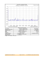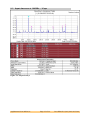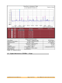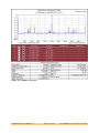
1
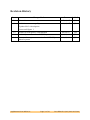
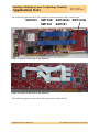
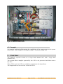
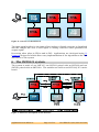
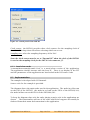
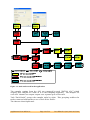
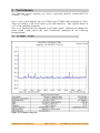
Sundance Multiprocessor Technology Limited
Application Note
Unit / Module Description:
1Gsps development platform
Unit / Module Number:
SMT8121
Document Issue Number:
1.4
Issue Date:
19/02/09
Original Author:
Jean-Philippe Arnaud
Form : QCF32
Date : 6 July 2006
Application Note
for
SMT8121
Sundance Multiprocessor Technology Ltd, Chiltern House,
Waterside, Chesham, Bucks. HP5 1PS.
This document is the property of Sundance and may not be copied
nor communicated to a third party without prior written
permission.
© Sundance Multiprocessor Technology Limited 2006
Application Note SMT8121
Last Edited: 19/02/2009 16:32:00
Revision History
Issue
Changes Made
Date
Initials
1.0
First release
15/06/07
JPA
1.1
Added resource usage figures
08/08/07
JPA
Updated kit’s description
Corrected figure 1
1.2
Added system power consumption
09/08/07
SM
1.3
Added system based on SMT395Q
30/10/08
JPA
1.4
Corrected comport connection for SMT395Q
based system
19/02/09
JPA
Application Note SMT8121
Page 2 of 26
Last Edited: 19/02/2009 16:32:00
Table of Contents
1
Introduction ..................................................................................................................... 5
2
Related Documents ........................................................................................................ 6
2.1
Referenced Documents.............................................................................................. 6
2.2
Applicable Documents............................................................................................... 6
3
Acronyms, Abbreviations and Definitions .............................................................. 6
3.1
Acronyms and Abbreviations ................................................................................... 6
3.2
Definitions.................................................................................................................... 6
4
Quick start........................................................................................................................ 7
4.1
What’s in the kit? ........................................................................................................ 7
4.2
Assembling the boards .............................................................................................. 8
4.3
Example....................................................................................................................... 11
5
Overview ........................................................................................................................ 11
6
The SMT8121 system .................................................................................................. 12
6.1
Sampling clock .......................................................................................................... 13
7
Hardware ........................................................................................................................ 14
8
A simple example ......................................................................................................... 15
8.1
Running the example ............................................................................................... 15
8.1.1 Connections........................................................................................................... 15
8.1.2 Running the software .......................................................................................... 15
8.1.3 Stand alone mode................................................................................................. 18
8.2
Implementation ......................................................................................................... 18
8.3
Building the example................................................................................................ 20
8.4
Resource usage.......................................................................................................... 20
9
Performance................................................................................................................... 21
9.1
No input – 1Gsps....................................................................................................... 21
9.2
Input sinewave at 100MHz – 1Gsps ...................................................................... 23
9.3
Input sinewave at 250MHz – 1Gsps ...................................................................... 24
10
System power consumption ...................................................................................... 26
11
Summary......................................................................................................................... 26
Application Note SMT8121
Page 3 of 26
Last Edited: 19/02/2009 16:32:00
Table of Figures
Figure 1: assembling the boards (SMT395) .......................................................................... 8
Figure 2: assembling the boards (SMT395Q)........................................................................ 9
Figure 3: picture of the front of the SMT8121................................................................... 10
Figure 4: picture of the back of the SMT8121 ................................................................... 10
Figure 5: SMT8121 inside the PC.......................................................................................... 11
Figure 6: overview of the SMT8121...................................................................................... 12
Figure 7: hardware description of the SMT8121 ............................................................... 12
Figure 8: SMT8121 control panel ......................................................................................... 16
Figure 9: control panel of the SMT391................................................................................ 17
Figure 10: control panel of the SMT381.............................................................................. 18
Figure 11: main tasks used in the application................................................................... 19
Figure 12: no input/1Gsps (J1) ............................................................................................. 21
Figure 13: no input/1Gsps (J2) ............................................................................................. 22
Figure 14: output from J1...................................................................................................... 23
Figure 15: output from J2...................................................................................................... 24
Figure 16: 250MHz/1Gsps (J1).............................................................................................. 25
Figure 17: 250MHz/1Gsps (J2) ............................................................................................ 26
Application Note SMT8121
Page 4 of 26
Last Edited: 19/02/2009 16:32:00
Sundance Multiprocessor Technology Limited
Application Note
Form : QCF32
Date : 6 July 2006
1 Introduction
The Sundance SMT8121 development platform is a modular system made of
multiple FPGAs and DSPs that can be used for multi-carrier / multi-standard cellular
systems, High Direct-IF infrastructures and test equipments.
It accommodates two input channels and two output channels each sampling at
1Gsps. Three Xilinx FPGAs (Virtex4 and VirtexII-pro) and one TI C64 DSP running at
1GHz are available for the processing of the signals.
The SMT8121 is fully supported by 3L Diamond design environment. Diamond
allows to easily and efficiently implement algorithms on the multiple DSPs and
FPGAs available in the system.
Application Note SMT8121
Last Edited: 19/02/2009 16:32:00
Sundance Multiprocessor Technology Limited
Application Note
Form : QCF32
Date : 6 July 2006
2 Related Documents
2.1 Referenced Documents
2.2 Applicable Documents
SMT310Q user manual
SMT391 user manual
SMT381 user manual
SMT368 user manual
SMT395 user manual
3L Diamond
Sundance Help File
3 Acronyms, Abbreviations and Definitions
3.1 Acronyms and Abbreviations
3.2 Definitions
Application Note SMT8121
Last Edited: 19/02/2009 16:32:00
Sundance Multiprocessor Technology Limited
Application Note
Form : QCF32
Date : 6 July 2006
4 Quick start
4.1 What’s in the kit?
The Smt8121 is made of the following hardware:
Name
Qty
Description
SMT310Q
1
PCI carrier board
SMT395-VP30
1
DSP board
SMT381
1
DAC board
SMT368A
1
FPGA board
SMT391
1
ADC board
SMT368
1
FPGA board
SMT500
5
FMS cables
SMT506
SMT507
or 4
MMBX—BNC or
analogue cable.
MMBX-SMA
SMT509-100
1
MMBX—MMBX cable (10 cm)
SMT596-H
1
Dual SHB<-> SHB module
SMT531-320
1
SHB cable, right angled
SMT516
1
SHB<-> SHB module
The Smt8121 requires the following software:
Name
Qty
Description
TI CCS
1
TI development environment
Xilinx ISE
1
Xilinx FPGA development environment
Diamond
1xDSP+2xFPGA
1
3L development environment
Diamond
1xFPGA
1
Optional – to target the FPGA of the SMT395
Application Note SMT8121
Last Edited: 19/02/2009 16:32:00
Sundance Multiprocessor Technology Limited
Application Note
Form : QCF32
Date : 6 July 2006
4.2 Assembling the boards
The following diagram shows the position of the boards on the SMT310Q and the
cable connections.
S
H
B
CP0
S
H
B
CP1
CP4
CP5
S
H
B
S
H
B
S
H
B
S
H
B
S
H
B
S
H
B
S
H
B
S
H
B
CP0
CP1
CP3
CP4
CP0
CP1
CP3
Figure 1: assembling the boards (SMT395)
Application Note SMT8121
Last Edited: 19/02/2009 16:32:00
Figure 2: assembling the boards (SMT395Q)
Application Note SMT8121
Page 9 of 26
Last Edited: 19/02/2009 16:32:00
Sundance Multiprocessor Technology Limited
Application Note
Form : QCF32
Date : 6 July 2006
The following pictures show the complete system with all cable connections.
SMT395
SMT368/ SMT368A/ SMT310Q
SMT391 SMT381
Figure 3: picture of the front of the SMT8121
Figure 4: picture of the back of the SMT8121
The following picture shows how the system fits inside the PC.
Application Note SMT8121
Last Edited: 19/02/2009 16:32:00
Figure 5: SMT8121 inside the PC
4.3 Example
An example application illustrating the capabilities of the components in the system
is provided. The example is developed using 3L Diamond design tool.
5 Overview
The SMT8121 system is made of a 1Gsps dual channel ADC and a 1Gsps dual
channel DAC.
The system allows samples captured by the ADC to be processed and then sent to
the DAC.
Three FPGAs and one DSP are available to implement the algorithms.
The diagram shows an overview of the SMT8121.
Application Note SMT8121
Page 11 of 26
Last Edited: 19/02/2009 16:32:00
Figure 6: overview of the SMT8121
The input signal applied to the input of the Analog to Digital converter is digitalized
and the samples are sent to the Digital to Analog Converter which generates the
output signal.
Processing takes place in FPGAs and in DSP. Applications are developed using 3L
Diamond design tool which allows easy implementation of the algorithm on the DSP
and FPGAs of the system.
6 The SMT8121 system
The system is made of one SMT395, one SMT391 paired with an SMT368 and one
SMT381 paired with an SMT368A. The modules are held on an SMT310Q PCI carrier
board.
Figure 7: hardware description of the SMT8121
Application Note SMT8121
Page 12 of 26
Last Edited: 19/02/2009 16:32:00
Samples are sent from the ADC to the DAC via SDB connection. Two 32-bits SDBs
running at 1/8 of the sampling frequency are used to transport the samples of each
channel.
A snapshot of the samples captured by the ADC is also sent to the DSP via two
comport connections. The DSP computes the FFT of the data and sends the raw
data and the result of the FFT to host to be displayed.
6.1 Sampling clock
For the system to work without loss of sample the sampling clocks of the ADC and
the DAC need to be the same.
There are two ways to supply the sampling clock to the ADC and the DAC. You can
either use the SMT391 on-board VCO or use an external signal generator.
1. Use the SMT391 on-board VCO
The SMT391 is configured to use its on-board VCO. The SMT381 is configured to
use external RF clock source.
The sampling clock generated on the SMT391 is provided to the SMT381 by
connecting SMT391-J8 to SMT381-J5.
The range of frequencies available goes from 600Msps to 1Gsps.
2. Use external clock
Both SMT391 and SMT381 are configured to use external sampling clock.
external signal generator is used to generate the sampling clock.
Application Note SMT8121
Page 13 of 26
An
Last Edited: 19/02/2009 16:32:00
Sundance Multiprocessor Technology Limited
Application Note
Form : QCF32
Date : 6 July 2006
7 Hardware
SMT395
SMT395 is based on the 1GHz 64-bit TMS320C6416T DSP, manufactured on the
latest 90nm wafer technology and offers the highest fixed-point processing power
ever. Sundance have not stopped here and have implemented a scalable solution
using Xilinx Virtex II Pro FPGAs .
SMT381
The SMT381 is a single width Daughter Module that plugs onto SLB base module
SMT368A (Virtex4 FPGA). It is capable of converting two external digital inputs
coming from the Virtex4 FPGA, using the SLB interface on the SMT368A, with a
resolution of 14 bits at 1Gsps. A Fujitsu dual channel DAC (MB86064) performs the
digital to analogue conversion.
SMT391
The SMT391 is a single width expansion TIM that plugs onto SLB base module
SMT368 (Virtex4 FPGA).
It is capable of sampling two analog inputs at 1 GSPS with a resolution of 8 bits. An
Atmel duel channel ADC (AT84AD001) performs the analogue to digital conversion.
SMT310Q
The SMT310Q is a quad (4) site module carrier developed to provide access to TIM
Modules over the PCI bus running.
The card has an ‘on-board’ JTAG controller allowing Code Composer Studio and 3L
Diamond applications to be used to debug/upload software to Modules.
Application Note SMT8121
Last Edited: 19/02/2009 16:32:00
Sundance Multiprocessor Technology Limited
Application Note
Form : QCF32
Date : 6 July 2006
8 A simple example
This simple example illustrates the functioning of the SMT8121. This example can
be used as a starting point for users to develop their own applications on the
SMT8121.
The samples of the ADC are looped back to the DAC. A copy of the samples is
routed to the DSP which computes an FFT on them and displays both the raw data
and the FFT result.
8.1 Running the example
8.1.1 Connections
Make sure all connections described in the “Quick start” section are made.
Connect a signal generator to the input of the SMT391 and a scope or spectrum
analyser to the output of the SMT381.
The amplitude of the input signal should be less than 400mV.
8.1.2 Running the software
Select project “com.sundance.example.smt8121”.
In the Diamond IDE click the run button to compile and run the example.
If you are using Diamond in command line, double click the .app file to run the
example.
The following windows should appear. The top two windows show the raw data
samples captured by the ADC. The bottom two windows display their FFT.
Application Note SMT8121
Last Edited: 19/02/2009 16:32:00
Figure 8: SMT8121 control panel
A graphical user interface allows the user to control the system.
SMT391 Control
The window “SMT391 control” allows configuring some of the settings of the
SMT391 board.
Application Note SMT8121
Page 16 of 26
Last Edited: 19/02/2009 16:32:00
Figure 9: control panel of the SMT391
Clock source: the SMT391 provides three clock sources for the sampling clock of
the ADC. This drop-down list allows selecting which one to use.
Sampling rate: select the sampling frequency of the ADC.
Channel I only: when selected, input J1 is sampled by both channels of the ADC.
When un-selected, inputs J1 and J2 are each sampled by one channel of the ADC.
Base board: select the base board used.
The section advanced should not be used when on-board clocks are used.
DRDA: the DRDA value depends on the sampling frequency and the base board
used. You may need to change this value if you are using external sampling clock as
the application then doesn’t know the sampling frequency. Refer to function
“calcDRDA()” in task ”Smt391Control.c” for the value to use.
SMT381 control
The window “SMT381 control” allows configuring some of the settings of the
SMT381 board.
Application Note SMT8121
Page 17 of 26
Last Edited: 19/02/2009 16:32:00
Figure 10: control panel of the SMT381
Clock source: the SMT391 provides three clock sources for the sampling clock of
the ADC. This drop-down list allows selecting which one to use.
Sampling rate: select the sampling frequency of the DAC.
Note: the clock source must be set to “External RF” when the clock of the SMT391
is used as the sampling clock for the SMT381 via connector J5.
8.1.3 Stand alone mode
“com.sundance.example.smt8121.sa” is a stand alone version of the application.
The application doesn’t interact with the host PC. There is no display of the FFT
and the parameters of the application are hard-coded in the DSP source code.
8.2 Implementation
The example is developed with 3L Diamond.
Source code for the example is provided.
The diagram shows the main tasks used in the application. The tasks in yellow run
on the DSP of the SMT395; the tasks in red run on the FPGA of the SMT368/391;
the tasks in blue run on the FPGA of the SMT368A/381.
To keep the diagram clear only the tasks playing a major role in the application are
shown.
The functionality and use of the tasks which don’t appear can usually be
deduced from their name and connection in the application.
Application Note SMT8121
Page 18 of 26
Last Edited: 19/02/2009 16:32:00
Figure 11: main tasks used in the application
The samples coming from the ADC are captured by task “SMT391_ADC” which
outputs four samples at a time at ¼ of the sampling frequency. The samples for
each ADC channel are output output on a separate port of the task.
Task “Pack32to64” groups the samples eight by eight. This grouping enables the
tasks connected afterwards to use a clock twice slower.
The data are then duplicated.
Application Note SMT8121
Page 19 of 26
Last Edited: 19/02/2009 16:32:00
One copy is sent to the storage task which captures a snapshot of the samples and
sends them to the “main” task for display and FFT processing. This is a non real
time loop.
The other copy is sent to task “split” which separates the samples coming on its
input channel on two output channels each having four samples. Each output
channel is mapped onto one SDB link linking the SMT368 to the SMT368A. Each
SDB runs at 1/8th the sampling frequency producing a data rate of 500MB/s.
On the SMT368A the samples are received by tasks “unsplit” which merges the data
arriving on its two input ports onto one output port.
The samples are then packed on 2 samples at a time and accelerated to 500MHz by
the task “pack64to16”.
Because the samples coming from the SMT391 are 8-bits and the DAC of the
SMT381 expects 14-bits samples, the task “scaler” multiplies each sample by a
constant value.
The samples are finally sent to task DAC381 which forwards them to the DAC on
the SMT381.
8.3 Building the example
Make sure that you have Xilinx ISE9.2sp4 as well as Diamond V3.1.10 or later
installed on your PC.
In the Diamond IDE, press CNTRL+B to build the application.
When using Diamond in command line, run the MAKE in directory
“com.sundance.example.smt8121\export” or
“com.sundance.example.smt8121.sa\export”.
8.4 Resource usage
The resource usage for the FPGA of the SMT391 is as follow:
BUFG
DCM
RAM16
SLICES
8 out of 32
1 out of 8
44 out of 192
2267 out of 15360
25%
12%
22%
14%
The resource usage for the FPGA of the SMT381 is as follow:
BUFG
DCM
RAM16
SLICES
8 out of 32
1 out of 8
16 out of 192
1998 out of 15360
25%
12%
8%
13%
Application Note SMT8121
Page 20 of 26
Last Edited: 19/02/2009 16:32:00
9 Performance
The following screen captures are from a spectrum analyser Anritsu-MS2717A
(100KHz – 7.1GHz).
Note 1: the system displays rays at 125MHz and 375MHz when sampling at 1Gsps.
These are images of the clock used by the SDB interfaces. They appear always at
1/8th of the sampling frequency.
Note 2: no filtering has been applied to the input signal. Filtering accordingly the
input signal could reduce the spur frequencies displayed in the following
measurements.
9.1 No input – 1Gsps
Figure 12: no input/1Gsps (J1)
Application Note SMT8121
Page 21 of 26
Last Edited: 19/02/2009 16:32:00
Figure 13: no input/1Gsps (J2)
Application Note SMT8121
Page 22 of 26
Last Edited: 19/02/2009 16:32:00
9.2 Input sinewave at 100MHz – 1Gsps
Figure 14: output from J1
Application Note SMT8121
Page 23 of 26
Last Edited: 19/02/2009 16:32:00
Figure 15: output from J2
9.3 Input sinewave at 250MHz – 1Gsps
Application Note SMT8121
Page 24 of 26
Last Edited: 19/02/2009 16:32:00
Figure 16: 250MHz/1Gsps (J1)
Application Note SMT8121
Page 25 of 26
Last Edited: 19/02/2009 16:32:00
Figure 17: 250MHz/1Gsps (J2)
10 System power consumption
The SMT8121 system power rail measurements show:
Power rail
Running the application
+12V
85mA
-12V
92mA
+5V
350mA
+3.3V
8.4A
11 Summary
Application Note SMT8121
Page 26 of 26
Last Edited: 19/02/2009 16:32:00