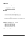
1
RCU Firmware V2.1
User Manual
Started: 15th April 2010
Last Update: 13th August 2010
DRAFT 0.1
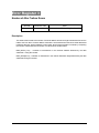
0.1 Index of Contents
RCU Firmware V2.1_______________________________________________ 1
User Manual ____________________________________________________ 1
0.1
Index of Contents ________________________________________________ 2
0.2
List of Tables ____________________________________________________ 3
0.3
List of Figures ___________________________________________________ 4
0.4
Updates (w.r.t) RCU_FW v2.0 _______________________________________ 5
Chapter 1 _______________________________________________________ 6
1.1
Functionality ____________________________________________________ 6
1.2
RCU/FEC Instruction Format _______________________________________ 8
1.3
Register Table ___________________________________________________ 9
1.4
RCU Memories and Address space _________________________________ 26
1.5
Instruction Sequencer Commands _________________________________ 27
1.6
front End Card Instructions _______________________________________ 32
1.7
RCU Commands ________________________________________________ 39
Chapter 2 ______________________________________________________ 50
2.1 Common Data Header (CDH) ____________________________________________ 51
2.2 Pay Load (ALTRO Read out Data) ________________________________________ 54
2.3 RCU Trailer ___________________________________________________________ 55
Appendix _____________________________________________________________ 66
0.2 List of Tables
1.1
IS Instruction Format _____________________________________________ 7
1.2
IS Internal Instruction Codes _______________________________________ 7
1.3
IS Internal Instruction format _______________________________________ 7
1.4
Configuration Registers of RCU ____________________________________ 8
1.5
Status & Error Registers of RCU ___________________________________ 20
1.6
Trigger Interface module Register set ______________________________ 22
1.7
Addressable Memories of RCU ____________________________________ 23
1.8
Structure of LOOP Instruction _____________________________________ 25
1.9
Content of Result Memory for Successful Loop Execution _____________ 25
1.10
Content of Result Memory for Failed Loop Execution _________________ 25
1.11
Structure of WAIT Instruction _____________________________________ 26
1.12
Content of Result Memory for WAIT Execution _______________________ 26
1.13
Structure of ENDSEQ Instruction __________________________________ 27
1.14
Content of Result Memory for ENDSEQ Execution ____________________ 27
1.15
Structure of ENDMEM Instruction __________________________________ 28
1.16
Content of Result Memory for ENDMEM Execution ___________________ 28
1.17
Structure of FEC_RD Instruction ___________________________________ 28
1.18
Content of Result Memory for Successful FEC_RD Execution __________ 31
1.19
Content of Result Memory for Failed FEC_RD Execution Execution _____ 31
1.20
Description of AIM error code in result memory for FEC RD ____________ 31
1.21
Description of Inst. Analyzer error code in result memory FEC_RD ______ 31
1.22
Structure of FEC_WR Instruction __________________________________ 32
1.23
Content of Result Memory for Successful FEC_WR Execution __________ 33
1.24
Content of Result Memory for Failed FEC_WR Execution Execution _____ 33
1.25
Description of AIM error code in result memory for FEC_WR ___________ 33
1.26
Description of Inst. Analyzer error code in result memory FEC_WR _____ 33
1.27
Structure of FEC_CMD Instruction _________________________________ 34
1.28
Content of Result Memory for Successful FEC_CMD Execution_________ 35
1.29
Content of Result Memory for Failed FEC_CMD Execution Execution ____ 35
1.30
RCU Commands ________________________________________________ 36
1.31
Structure of Event data block _____________________________________ 46
2.1
Common Data Header (CDH) ______________________________________ 47
2.2
Error & Status Bit in CDH 4[27:12] _________________________________ 49
2.3
Order of 10 bit words in 32 bit data packet __________________________ 50
2.4
RCU Trailer_____________________________________________________ 51
.3
List of Figures
1.1
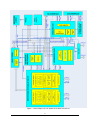
Block Diagram of Top Level Module of the RCU Firmware ______________ 6
1.2
FEC Read Chronogram ___________________________________________ 30
1.3
FEC Write Chronogram ___________________________________________ 32
1.4
CONFGFEC - Chronogram ________________________________________ 40
1.5
Software Triger Chronogram ______________________________________ 43
Updates w.r.t Version 2.0
1) Readout List Memory (ROLM)
Read out list memory is split into two separate memories, one is specified for each branch A
and B. Size of each memory is 12 * 2048.
Address space allocated to the ROLM – A is 0x1000 – 0x17FF
Address space allocated to the ROLM – A is 0x1800 – 0x1FFF
2) Hit List Memory (HLM)
Hit list memory is split into two separate memories, one is specified for each branch A and B.
Size of each memory is 32 * 64 (four consecutive locations specified for each FEC).
Address space allocated to the HLM – A is 0x 5000 – 0x 503F
Address space allocated to the HLM – B is 0x 5040 – 0x 507F
3) SCEVL Delay
Time to perform the scan event length command is configurable. This is the time taken
by the board controller to read the content of ADEVL register from ALTROs . This register is
set to a default value of 90 usec: = 0xE10 for TPC.
Address of this register is 0x510A and its 13 bit wide.
4) Configurable Frequency of Slow Control Clock
Slow control clock is provided from RCU to the FECs , the frequency of this clock is
configurable.
Address of this register is 0x800C and its 2 bit wide.
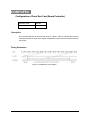
Chapter
0B
1
Top Level Unit
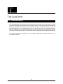
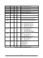
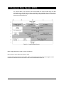
1.1 functionality
2B
The data/configuration transfer between the RCU and front-end cards is performed with the ALTRO
protocol as described in the ALTRO Chip User’s Manual. From the User’s point of view the ALTROs are
not directly accessible from the RCU. The link is made through a controller-like procedure that will
execute sequentially a set of pre-loaded instructions. In this way the user can send large portions of
front-end configuration in an instruction memory in the RCU and execute the sequence with a single
command. These sequences can be composed with ALTRO instructions and RCU-specific instructions.
This manual contains full information on all accessible memories and registers along with the
executable commands.
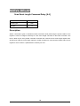
6
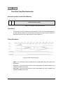
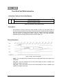
Figure 1.1: Block Diagram of TOP Module of the RCU Firmware 2.1
7
1.2 RCU/FEC Instruction Format
3B
An important difference between v1 and v2 of the RCU firmware regards the
Instruction Sequencer (IS). In the new version the IS can execute ALTRO
Instructions but not RCU Instructions. In addition the IS recognizes a set of 4 internal
instructions that can be used to condition the execution of the ALTRO instructions.
The Instruction Memory (IM) of the IS has in RCU v2 a depth of 4096 x 22-bit wide
words. The format of the Instructions for the IS is illustrated in tables 1.1, 1.2 and 1.3.
21
IS/FEC
20
19
INSTRUCTION PARAMETERS
00, FEC_RD
ALTRO Instruction
01, FEC_CMD
ALTRO Instruction
ALTRO Instruction (Address)
10, FEC_WR (*)
11, IS_CMD
0
ALTRO Instruction (Data)
IS Internal Code parameter (16
bits)
IS Internal Code (4 bits)
Table 1.1 IS Instruction Format
Name
Access
Inst. Code
Description
LOOP
W
0x1
Execute the instructions in loop for defined number of times
WAIT
W
0x2
Wait for defined number of clock cycles
ENDSEQ
W
0x8
End of specific sequence (set of instructions)
ENDMEM
W
0xF
End of Instruction Memory
Table 1.2. IS internal instructions codes.
IS/FEC
IS CMD
CMD PARAMETER
11
Wait
Number of wait cycles
11
Loop
11
ENDSEQ
X
11
ENDMEM
X
No of loops
[15:12]
Loop return address[11:0]
Table 1.3. IS internal instruction format.
8
1.3
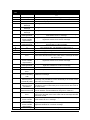
Configuration Registers
The register Table 1.4, incorporates various registers that are used for configuration of the
RCU. Table 1.5 and table 1.6 describes the status and error register which can be read
externally for RCU and trigger module respectively.
Name
Addres
s
Width
Access
Description
ACTFECLIST
0x5100
32
W/R
Active FEC List
ALTROIF
0x5101
18
W/R
Nr. Samples / channel ≡ [9:0];
Tsampling / TLHC ≡ [13:10];
CSTB programmable delay ≡ [15:14] ;
Instruction error check selection [17:16]
TRGCONF
0x5102
17
W/R
Trigger Source ≡ [16:14], Trigger Mode ≡
[13], L2 latency wrt L1 ≡ [12:0].
RDOMOD
0x 5103
4
W/R
[3] Mask RDYRX ;Sparse readout enable
≡ [2]; execute sequencer on SOE/EOE ≡
[1] ;
MEB mode [0].
ALTROCFG1
0x5104
20
W/R
Copy of the ALTROCFG1 register of the
ALTRO chip (see ALTRO manual pags.
36-37). The content of this register will be
copied in one of the words of the event
data block trailer.
ALTROCFG2
0x5105
25
W/R
Copy of the ALTROCFG2 register of the
ALTRO chip (see ALTRO manual pags.
36-37). The content of this register will be
copied in one of the words of the event
data block trailer.
RCU_VERSION
0x5106
24
R
BP_VERSION
0x5107
1
W/R
Mapping of ACTFECLIST to cardswitch
lines. 0 for TPC and FMD, 1 for PHOS.
RCUID
0x5108
9
W/R
RCU ID Register
SCEVL_DLY
0x510A
13
W/R
Time to perform SCEVL command
SCLK_FREQ
0x800C
2
W/R
Frequency of the slow control clock is
configured in this register.
RCU version (ASCII coding of version
number).
Table 1.4 Configuration Registers of RCU
9
ACTFECLIST
Active Front End Card List [31:0]
Address
Access Type
Bit Width
0x5100
R/W
31
Description:
Front end cards are set turned on and off by configuring this register.
FEC – Branch A [15:0]
FEC – Branch B [31:16]
10
ALTROIFQQ
ALTRO Interface Register [17:0]
Address
0x5101
Access Type
Bit Width
R/W
18
Description:
Instruction error check selection ≡ [17:16]
“00”:= Contents of Instruction memory are not Checked
“01”:= Contents of Instruction memory will be checked against TPC instruction set.
“10”:= Contents of Instruction Memory will be checked against PHOS instruction set.
“11”:= Contents of Instruction Memory will be checked against FMD instruction set
CSTB programmable delay ≡ [15:14]
This is the delay between the assertion of “cstb” and altro bus to avoid any possibility of glitch on
hand shake
signals due to 40 bit ALTRO bus driving.
Sampling Clock Dividing Ratio: T sampling / TLHC ≡ [13:10]
“00”:= divide by 2; Period of sampling clock = 50nsec
“01”:= divide by 4; Period of sampling clock = 100nsec
“10”:= divide by 8; Period of sampling clock = 200nsec
“11”:= divide by 16; Period of sampling clock = 400nsec
Nr. Samples / channel ≡ [9:0]
11
TRGCONFQQ
Trigger Configuration Register [16:0]
Address
0x5102
Access Type
R/W
Bit Width
17
Description:
Trigger Source [16:14]
i)
ii)
iii)
iv)
“100” ≡ CTP – Triger Enabled
“110” ≡ L1 pulse is used as Trigger input. Serial B input is ignored.
“001” ≡ Software Trigger Enable (0x5306)
“010” ≡ Auxiliary Trigger Enable. This trigger pulse is directly injected to RCU.
Trigger Mode [13]
‘0’ ≡ Trigger mode is TPC {L1 from CTP is mapped to L1 to FEC}
‘1’ ≡ Trigger mode is PHOS {L0 from CTP is delivered as L1 to FEC}
L1 – L2 Latency [12:0]
For trigger sources (ii, iii and iv) the latency between L1 and L2 is set here.
12
RDOMODQQ
Readout Mode Configuration Register [3:0]
Address
0x5103
Access Type
Bit Width
R/W
5+2(Debug mode)
Description:
Skip Empty Channel [6]
[6] = “1” ≡ RCU will skip the empty channel while performing “Full Readout”
[5] = “0” ≡ RCU will not skip the empty channel while performing “Full Readout”
Mask Check of [Channel Address / Block Length] Mismatch [5][4]
[5] = “1” ≡ check of Channel address mismatch will be masked (not checked)
[5]= “0” ≡ check of Channel address mismatch will not be masked (checked)
[4] = “1” ≡ check of Block Length mismatch will be masked (not checked)
[4]= “0” ≡ check of Block Length mismatch will not be masked (checked)
Mask Read to Receive “RDYEX” [3]
“1” ≡ Ready to receive command is masked, means even if the ready to receive
command is not given from DDL still data will be delivered from RCU to SIU.
{Used for debugging purposes}
“0” ≡ Ready to receive command (open link) must be given before data is to be
received.
Sparse Readout Mode [2]
‘0’ ≡ Read out mode is “full readout” according to readout list memory.
‘1’ ≡ Read out mode is “sparse readout” according to readout list memory.
U
U
U
U
SOE/EOE Instruction Memory Execution [1]
‘0’ ≡ Sequence in the instruction memory will not be executed on SOE/EOE.
‘1’ ≡ Sequence in the instruction memory will be executed on SOE/EOE and
result from result memory will be sent as payload.
MEB (multi event buffer) Mode [0]
‘0’ ≡ Multi event buffer mode is set to 4
‘1’ ≡ Multi event buffer mode is set to 8
13
ALTROCFG111GGQQ
ALTRO Configuration Register 1 [19:0]
Address
0x5104
Access Type
R/W
Bit Width
20
Description:
This register is copy of ALTRO configuration register. Parameters in this register are used to
record in the RCU trailer word. Refer to ALTRO manual pages 36, 37.
First Baseline Correction Mode ≡ RDO_
CFG1 [3:0]
Polarity. When set, the ADC data is inverted (1’s C) [4]
nd
Nr. Of pre-samples excluded from 2 baseline corr. ≡ RDO_CFG1 [6:5]
nd
Nr. Of post-samples excluded from 2 baseline corr. ≡ RDO_CFG1 [10:7]
Enable second baseline correction ≡ RDO_CFG1 [11]
Glitch filter configuration for zero suppression ≡ RDO_CFG1 [13:12]
Nr. Of post-samples excluded from suppression
Nr. Of pre-samples excluded from suppression
≡ RDO_CFG1[16:14]
≡ RDO_CFG1[18:17]
Enable Zero Suppression ≡ RDO_
CFG1 [19]
14
ALTROCFG2Q
Altro Configuration Register 2 [24:0]
Address
Access Type
Bit Width
0x5105
R/W
25
Description:
Nr of ALTRO Buffers (copy of RCU register ALTROCFG2[4]) = RDO_CFG2[24]
Nr of pre-trigger samples (copy of RCU register ALTROCFG2[[3:0]) = RDO_CFG2[23:20]
Nr. Samples / channel (copy of RCU register ALTROIF[9:0]) = RDO_CFG2[19:10]
Sparse Readout = RDO_CFG2[9]
Tsampling / TLHC = RDO_CFG2[8:5]
Phase of L1 trigger w.r.t. LHC bunch crossing = RDO_CFG2 [4:0].
The phase is calculated in terms of bunch crossing cycles for example if the T sampling/TLHC
is equal 01 (10MHz sampling rate), only the two least significant bits are meaningful and the phase
can take values 0, 1, 2, 3.
15
RCU_VERSIONQQ
RCU Version Register [23:0]
Address
0x5106
Access Type
R
Bit Width
24
Description:
This register describes the RCU version along with the revision, format is “MM-YY-AE-VERSION”
read as X"07-08-AE-20"
Month Year: = 0708
Version: = 2.0
Identification: = AE
16
BP_VERSIONQQ
Back Plane Version Register [0]
Address
0x5107
Access Type
R
Bit Width
1
Description:
This register set the mapping structure of ACTFECLIST to card switch lines.
‘0’:= TPC and FMD.
‘1’:= PHOS.
17
RCUIDQQ
RCU Identification Register [8:0]
Address
Access Type
Bit Width
0x5108
R/W
9
Description:
This register identifies the physical location of RCU.
RCUID [8] = 0 for A-side, 1 for C-side
RCUID [7:3] = sector number (0:17)
RCUID [2:0] = readout partition number (0:5)
18
SCEVL DELAY
Scan Event Length Command Delay [8:0]
Address
Access Type
Bit Width
0x510A
R/W
13
Description:
SCEVL command is given in broadcast mode to all FECs while performing the sparse readout. This
register is used to configure the delay for scan event length command to the board controller. This
time is taken by the every board controller to transfer the contents of the event length register from
ALTRO and build the event length register in board controller for 128 channels. Default value of this
register is set to “0xE10”:= (3600*25nsec= 90usec) for TPC.
19
SCLK_FREQ
Frequency of the Slow control clock [1:0]
Address
0x800C
Access Type
R/W
Bit Width
2
Description:
Slow control clock is provided to board controller to perform the readout of monitoring parameters.
The frequency of this clock is configurable as described below:
Value
Frequency(MHz)
0x0
5.0
0x1
2.5
0x2
1.25
0x3
0.625
20
Name
Address
Width
Access
FECERRA
0x 5110
20
R
FECERRB
0x 5111
20
R
Description
Error code , transactions on branch A
[ 0] Altro Error is asserted.
FSM_WR
[ 1] Altro assert error before ”cstb” assert
[ 2] “ack” assert before “cstb”
[ 3] Altro assert error during ‘waitack’
[ 4] “ack” not asserted & time out
[ 5] Altro error asserted during ‘waitdone’
[ 6] “ack” not released by Altro
[ 7] Altro Assert the error while waiting for broad cast
command
FSM_RD
[ 8] Altro error is asserted during ‘assertbus’
[ 9] Altro error is asserted while waiting for “ack”
“chlack”
[10] Altro assert “ack” before “cstb” assert
[11] Altro error is asserted while waiting for “ack”
[12] Altro does not assert ack
[13] Altro error is asserted while waiting for release
of “ack”
[14] “ack” never released by Altro
FSM_RDO
[15] Fsm wr error when started by FSM RDO
[16] Altro error asserted before transfer asserted.
[17] Transfer not asserted
[18] Altro error asserted while data being transferred
[19] Transfer not released
Error code , transactions on branch A
[ 0] Altro Error is asserted.
FSM_WR
[ 1] Altro assert error before ”cstb” assert
[ 2] “ack” assert before “cstb”
[ 3] Altro assert error during ‘waitack’
[ 4] “ack” not asserted & time out
[ 5] Altro error asserted during ‘waitdone’
[ 6] “ack” not released by Altro
[ 7] Altro Assert the error while waiting for broad cast
command
FSM_RD
[ 8] Altro error is asserted during ‘assertbus’
[ 9] Altro error is asserted while waiting for “ack”
“chlack”
[10] Altro assert “ack” before “cstb” assert
[11] Altro error is asserted while waiting for “ack”
[12] Altro does not assert ack
[13] Altro error is asserted while waiting for release
of “ack”
[14] “ack” never released by Altro
FSM_RDO
[15] Fsm wr error when started by FSM RDO
[16] Altro error asserted before transfer asserted.
[17] Transfer not asserted
[18] Altro error asserted while data being transferred
21
[19] Transfer not released
Errors related to Event Read out
[0]Error occur during send command
[1]Atlro error when wait trsf assert
[2]Trsf not assert
[3]Altro not give four dstb data
[4]Trsf not release
[5]Error occur during send scan event length
command
[6] RD_RX not asserted or de-asserted during event
readout
[7] Channel Address mismatch
[8] Data Block Length mismatch
Debug
[31:28] FSMWR_ST_B
[27:24] FSMWR_ST_A
[23:20] FSMEVLEN_ST
ALTRO bus status refreshed every clock cycle:
[0] CSTB, branch A
[1] ACK, branch A
[2] TRSF, branch A
[3] CSTB, branch B
[4] ACK, branch B
[5] TRSF, branch B
[6] L1 of ALTRO
[7] L2 of ALTRO
ALTRO bus status(when TRSF_A or TRSF_B is
asserted):
[0] CSTB, branch A
[1] ACK, branch A
[2] TRSF, branch A
[3] CSTB, branch B
[4] ACK, branch B
[5] TRSF, branch B
[6] L1 of ALTRO
[7] L2 of ALTRO
RCU bus is busy(running instruction sequencer)
[0] instruction sequencer busy
[1] Last instruction sequence completed with errors
[3:0] MEB status counter
Debug
[7:4] DATA_READY
[9:8] DM_SEL :- it shows which of memory
block(out of A0,A1,B0,B1) is being read by the data
assembler.
RDOERR
0x5112
9
R
ALTBUSST
ATUS
0x5114
8
R
ALTBSST_
TRSF
0x5115
8
R
BUSBSY
0x5116
2
R
MEBST
CNT
0x511B
4
R
SWTTRGC
NT
0x511C
20
R
Software Trigger counter
AUXTRGC
NT
0x511D
20
R
Auxiliary Trigger counter
TTCL2_AC
NT
0x511E
20
R
TTC L2 Accept Counter
TTCL2_RC
NT
0x511F
20
R
TTC L2 Reject Counter
DSTB_A
CNT
0x5120
20
R
Branch A DSTB Assert Counter
DSTB_B
CNT
0x5121
20
R
Branch B DSTB Assert Counter
22
TRSFA CNT
0x5122
12
R
Branch A TRSF Assert Counter
TRSFB CNT
0x5123
12
R
Branch B TRSF Assert Counter
ACKA CNT
0x5124
12
R
Branch A ACK Assert Counter
ACKB CNT
0x5125
12
R
Branch B ACK Assert Counter
CSTBA CNT
0x5126
12
R
Branch A CSTB Assert Counter
CSTBB CNT
0x5127
12
R
Branch B CSTB Assert Counter
DSTB_NUM
A
0x5128
9
R
Block length of last data written from Branch A
DSTB_NUM
B
0x5129
9
R
Block length of last data written from Branch B
ADD_MM_C
NT
0x512A
12
R
Number of address mismatches between ALTRO
trailer and addressed channel from ROLM.
BLTH_MM_
CNT
0x512B
12
R
ABDFSMPR
_ST
0x512C
22
R
RDOFSMPR
_ST
0x512D
15
R
INSSEQ
PR_ST
0x512E
15
R
EVMNGPR_
ST
0x512F
12
R
DA_FSM
0x5130
RDO_TIME*
0x5132
Number of block length mismatches between
ALTRO trailer word and the (data strobe counter –
1)
ABD state machines status
[21:19] FSM_RDO status of branch B
[18:15] FSM_RD status of branch B
[14:11] FSM_WR status of branch B
[10:8]
FSM_RDO status of branch A
[7:4]
FSM_RD status of branch A
[3:0]
FSM_WR status of branch A
Readout state machines status
[14:12] SCEVLEN_FSM status
[11:8] EVLEN_FSM status
[7:4]
FSM_EVRDO_CTRL status
[3:2]
FSM_SEL_BR status of branch B
[1:0]
FSM_SEL_BR status of branch A
Execute instruction sequencer state machines
status
[14:10] FSM_INSTSEQ status
[9:5]
FSM_INSTLOOP status
[4:0]
FSM_RU status
Event manager state machines status
[11:10] FSM_TST_TRG status
[9:6]
FSM_TTC_TRG status
[5:3]
FSM_EV status
[2:0]
FSM_INSSEQ status
[29:25] fsmrdrm_st ,
[ 24:20] fsmrdpar_st ,
[19:15] fsmrddm_st ,
[14:10] fsmrdcdhsoft_st ,
[9:5] fsmrdcdh_st ,
[0:4] fsmdamain_st
Time taken by last event readout (L2 ---- EOEV)
[RDO_TIME*25= TIME IN nsec)
R
32
R
Table 1.5 Status & Error Registers of RCU
23
Name
Address
Access
Description
Control[23:0]
0x 4000
RW
Module Reset
0x4001
T
RoI_Config1[17:0]
0x4002
RW
Definition of what region of interest the RCU is a part of
(depends on the sector). Bit 17:0
RoI_Config2[17:0]
0x4003
RW
Definition of what region of interest the RCU is a part of
(depends on the sector). Bit 35:18
Reset Counters
0x4004
T
Write to this registers will reset the counters in the module
Issue Testmode
0x4005
T
Debug: Issues testmode sequence. Note that serialB
channel input MUST be disabled when using this feature.
L1_Latency[15:0]
0x4006
RW
L2_Latency[31:0]
0x4007
RW
RoI_Latency[31:0]
0x4009
RW
L1_msg_latency[31:0]
0x400A
RW
Pre_pulse_counter[15:0]
0x400B
R
[15:12] Uncertainty region +- N. default value 0x2 (50 ns)
[11:0] Latency from L0 to L1, default value 0x0D4 (5.3 us)
[15:0] Max Latency from BC0 to L2, default
value 0x4E20 (500 us)
[31:16] Min Latency from BC0 to L2, default
value 0x0C80 (80 us)
[15:0] Max Latency from BC0 to RoI msg
[31:16] Min Latency from BC0 to RoI msg
[15:0] Max Latency from BC0 to L1 msg, default value
0x0028 (1 us)
[31:16] Min Latency from BC0 to L1 msg, default value
0x0F8 (6,2 us)
Number of decoded pre-pulses.
BCID_Local[11:0]
0x400C
R
Number of bunchcrossings at arrival of L1 trigger.
L0_counter[15:0]
0x400D
R
L1_counter[15:0]
0x400E
R
Number of L1 triggers
L1_msg_counter[15:0]
0x400F
R
Number of successfully decoded L1 messages
L2a_counter[15:0]
0x4010
R
Number of successfully decoded L2a messages
L2r_counter[15:0]
0x4011
R
Number of successfully decoded L2r messages
RoI_counter[15:0]
0x4012
R
Number of successfully decoded RoI messages
Bunchcounter[11:0]
0x4013
R
Debug: Number of bunchcrossings
[0] Serial B channel on/off Default: 1
[1] Disable_error_masking 0
[2] Enable RoI decoding 0
[3] L0 support 1
[4:7] (Not Used)
[8] L2a FIFO storage mask 1
[9] L2r FIFO storage mask 1
[10] L2 Timeout FIFO storage mask 1
[11] L1a message mask 1
[12] Trigger Input Mask Enable 0
[13:15] (Not Used)
[16] Bunch_counter overflow [17] Run Active [18] Busy (receiving sequence) [19] Not Used
[23:20] CDH version 0x2
[31:24] Trigger Receiver Version 0x13
Reset Module
Number of L0 triggers
24
Name
Address
Access
ErrorCnt[31:0]
0x4017
R
Buffered_events[4:0]
DAQ_Header01[31:0]
DAQ_Header02[31:0]
DAQ_Header03[31:0]
DAQ_Header04[31:0]
DAQ_Header05[31:0]
DAQ_Header06[31:0]
DAQ_Header07[31:0]
Event_info[17:0]
0x4020
0x4021
0x4022
0x4023
0x4024
0x4025
0x4026
0x4027
0x4028
R
R
R
R
R
R
R
R
R
Event_error [24:0]
0x4029
R
hammingErrorCnt[31:0]]
0x4016
R
Description
[15:0] Number of single bit hamming errors
[31:16]Number of double bit hamming errors
[15:0] Number of message decoding errors [31:16]
Number of errors related to sequence and timeouts.
Number of events stored in the FIFO.
Latest received DAQ Header 1
Latest received DAQ Header 2
Latest received DAQ Header 3
Latest received DAQ Header 4
Latest received DAQ Header 5
Latest received DAQ Header 6
Latest received DAQ Header 7
Latest Received Event information:
[0] RoI enabled
[1] Region of Interest announced (=ESR)
[2] RoI received
[3] Within region of interest
[4:7] Calibration/SW trigger type (= RoC)
[8] Software trigger event
[9] Calibration trigger event
[10] Event has L2 Reject trigger
[11] Event has L2 Accept trigger
[12] Include payload
[17:13] SCLK phase when (L0/L1)trigger arrives
[0] Serial B Stop Bit Error
[1] Single Bit Hamming Error Individually Addr.
[2] Double Bit Hamming Error Individually Addr.
[3] Single Bit Hamming Error Broadcast.
[4] Double Bit Hamming Error Broadcast.
[5] Unknown Message Address Received
[6] Incomplete L1 Message
[7] Incomplete L2a Message
[8] Incomplete RoI Message
[9] TTCrx Address Error (not X”0003”)
[10] Spurious L0
[11] Missing L0
[12] Spurious L1
[13] Boundary L1
[14] Missing L1
[15] L1 message arrives outside legal timeslot
[16] L1 message missing/timeout
[17] L2 message arrives outside legal timeslot
[18] L2 message missing/timeout
[19] RoI message arrives outside legal timeslot
[20] RoI message missing/timeout
[21] Pre pulse error (=0; possible future use)
[22] L1 message content error
[23] L2 message content error
[24] RoI message content error
Table 1.6 Trigger interface module register set
25
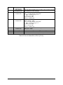
1.4 RCU Memories and Address space
5B
RCU contains a number of memories to execute the block transactions and to
perform the event readout. These memories and their description are given in
table 1.7
Name
Address
Size
Access
Description
Instruction Memory
0x 0000 – 0x 0FFF
*SPM
22x4K
W/R
Contains instructions to be
executed by *IS
Read out List
Memory Branch -A
0x 1000– 0x 17FF
SPM
12x2K
W/R
Configured with the channel
addresses for event readout
Read out List
Memory Branch –B
0x 1800– 0x 1FFF
SPM
12x2K
W/R
Result Memory
0x 2000 – 0x 37FF
SPM
25x 6K
W/R
It contains result of each
transaction by IS
TTCRx Register set
0x 4000 – 0x 4FFF
Register
s of
various
sizes
W/R
These registers are used in
TTCRx module
Hit List Memory
Branch - A
0x 5000 – 0x 503F
*DPM
32x64
Hit List Memory
Branch - B
0x 5040 – 0x 507F
*DPM
32x64
W/R
Configured by Board
Controllers with list of active
channels for all FECs in
Branch B
Data Memories
0x 5800 – 0x 5FFF
DPM
8*(20x2
56)
W/R
Contains the event data, from
FECs
Configured by Board
Controllers with list of active
channels for all FECs in
Branch A
Table 1.7 Addressable Memories of RCU
26
1.5 Instruction Sequencer Commands
6B
There are four internal instructions for the Instruction Sequencer (IS) which controls the
execution of instructions from instruction memory. Result of these internal commands is
loaded in the result memory as well. In this section detail structure of these commands in the
instruction memory and the respective result in the result memory is described.
27
LOOPInstruction Sequencer Loop
Instruction Coding in Instruction Memory
21
20
1
1
19
16 15
12
Number of
Loops
0001
0
11
Loop Return Address
Table 1.8 Structure of LOOP instructions.
Description
This command is used as internal instruction of the sequencer to repeat a set of instructions
for specific number of times. The iteration is made for the specific number of times till the loop
return address. Parametric structure for loop command is shown in table 1.8
Result of “LOOP” in the Result Memory
Result of this instruction is loaded in the result memory. Status bit [20] shows the success or
failure of the execution. 0: success; 1: failure. Table 1.9 and 1.10 shows the result of
execution for successful or failed execution respectively.
24
21
0100
20
19
0
16
15
12
0
11
Number of
Loops
Zeros
Loop Return Address
Table 1.9: Content of result memory for successful execution of loop.
24
21
0100
20
1
19
14
Zeros
13
0
10 9
Error Loop
Number
Number of Errors
Table 1.10: Content of result memory for failed execution of loop.
28
WAITInstruction Sequencer Wait
Instruction Coding in Instruction Memory
21
20
1
19
1
16
15
0
Number of wait cycles (40MZ CLK)
0010
Table 1.11: Structure of WAIT instruction
Description
This command is used as internal instruction of the sequencer to wait for specified number of
clock cycles. Parametric structure for WAIT command is shown in table 1.11
Result of “WAIT” in the Result Memory
Result of this instruction is loaded in the result memory. Table 1.12 shows the result of
execution.
24
21
0101
20
0
19
16 15
Zeros
0
Number of wait cycles (40MZ CLK)
Table 1.12: Content of result memory for the execution of Wait
29
ENDSEQQQ
End OF Sequence
Instruction Coding in Instruction Memory
21
20
1
1
19
0
16 15
1000
X
Table 1.13: Structure of ENDSEQ instruction.
Description
This command is used as internal instruction of the sequencer to end a set of instructions.
Parametric structure for ENDSEQ command is shown in table 1.13
Result of “ENDSEQ” in the Result Memory
Result of this instruction is loaded in the result memory along with the address of last
instruction executed. Table 1.14 shows the result of execution for ENDSEQ.
24
21
0111
20
0
19
0
12 11
Zeros
Address of last executed instruction
Table 1.14: Content of result memory for ENDSEQ.
30
ENDMEMQQ
Instruction Sequencer End of memory
Instruction Coding in Instruction Memory
21
20
1
1
19
0
16 15
1111
X
Table 1.15 Structure of ENDMEM instruction.
Description
This command is used to declare that end of memory has reached. Parametric structure for
ENDMEM command is shown in table 1.15
Result of “ENDMEM” in the Result Memory
Result of this instruction is loaded in the result memory along with the address of last
instruction executed. Table 1.16 shows the result of execution for ENDMEM.
24
21
0111
20
0
19
0
12 11
Zeros
Address of last executed instruction
Table 1.16 Content of result memory for ENDSEQ.
31
1.6 Front End Card Instructions
There are three instructions which can be executed through the instruction sequencer. These
instructions are to perform three different functions in FECs, read, write or command. Results
of these instructions are loaded in the result memory regardless of successful or failed
execution. In this section detail structure of these instructions for the instruction memory and
the respective result in the result memory is described.
32
FEC_RDFront End Card Read Instruction
Instruction Coding in Instruction Memory
21
20
0
0
19
0
Altro Instruction Format
Table 1.17: Structure of FEC_RD instruction.
Description
This instruction is used to perform the read operation on FEC. Any addressable location of
ALTRO or Board controller can be read using this instruction through instruction sequencer.
Parametric structure for FEC_RD instruction is shown in table 1.17
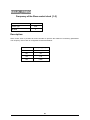
Timing Parameters
Figure1.2 FEC- read chronogram.
Pgdly = The command strobe is asserted after this programmable delay with respect to the
ALTRO bus.
Tout_ack1 = This is the maximum time for which acknowledge from FEC is awaited to get
asserted, 40 readout clock cycles.
Tout_ack2 = This is the maximum time for which acknowledge from FEC is awaited to get
released, 40 readout clock cycles.
33
Result of “FEC_RD” in the Result Memory
Result of this instruction is loaded in the result memory. Result of each read instruction
comprises of two locations of the result memory. Status bit [20] shows the success or failure
of the execution. 0: success; 1: failure. Table 1.18 ad 1.19 shows the result of execution for
successful or failed execution respectively.
24
21
20
0000
19
0
FEC Address from instruction memory for current instruction
0
Data Read from FEC
Table 1.18: Content of result memory for successful execution of FEC_RD.
24
21
20
0000
19
1
0
FEC Address from instruction memory for current instruction
“0000000”; AIM Error Code [10:6] ; Instr error code [5 :0]
Table 1.19: Content of result memory for failed execution of FEC_RD.
AIM Error
Code [10:6]
Description
01001
Altro Error line is asserted before “cstb” is asserted from RCU
01010
Altro Error line is asserted before the “ack” from FEC
01011
Altro asserts the “ack” before “cstb” ” is asserted from RCU
01100
Altro asserts error while RCU wait for “ack”
01101
Altro does not assert “ack” time out 1 occurs.
01110
Altro error is asserted while waiting the release of “ack”
01111
ALTRO doesn’t release the “ack” time out 2 occurs.
Table 1.20: Description f the AIM error code in the result memory for read transaction.
Bit Number
Instr error code [5 :0] Description
0
This bit is set if there has been an error in loop instruction
1
This error bit is set if the format of instruction sequencer command is not
correct.
2
This bit is set if the format of instruction to board controller is not correct.
3
This bit is set if the board controller at “Off FEC” is addressed, checked
w.r.t. FEC_ACTIVE LIST
4
This bit is set if the format of instruction to ALTRO is not correct.
5
This bit is set if ALTRO at “Off FEC” is addressed, checked w.r.t.
FEC_ACTIVE LIST
Table 1.21: Description of the instruction Analyzer error code in the result memory for read
transaction.
34
FEC_WRFront End Card Write Instruction
Instruction Coding in Instruction Memory
21
20
1
0
0
19
Altro Instruction Format
Data to be written to FEC
Table 1.22: Structure of FEC_WR instruction.
Description
This instruction is used to perform the write operation on FEC. Any write able location of
ALTRO or Board controller can be written using this instruction through instruction sequencer.
Each write instruction consists of two locations, first one contains the instruction parameters
same as ALTRO, next subsequent location contains the data for the write transaction.
Parametric structure for FEC_WR instruction is shown in table 1.22
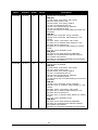
Timing Parameters
Figure 1.3 FEC- write Chronogram.
Pgdly = The command strobe is asserted after this programmable delay with respect to the
ALTRO bus.
Tout_ack1 = this is the maximum time for which acknowledge from FEC is awaited to get
asserted, 40 readout clock cycles.
Tout_ack2 = This is the maximum time for which acknowledge from FEC is awaited to get
released, 40 readout clock cycles.
35
Result of “FEC_WR” in the Result Memory
Result of this instruction is loaded in the result memory. Result of each write instruction
comprises of two locations of the result memory. Status bit [20] shows the success or failure
of the execution. ‘0’: success; ‘1’: failure. Table 1.23 ad 1.24 shows the result of execution for
successful or failed execution respectively.
24
21
20
0010
0
0
19
FEC Address from instruction memory for current instruction
Data written to FEC from Instruction memory
Table 1.23: Content of result memory for successful execution of FEC_WR.
24
21
20
0010
1
0
19
FEC Address from instruction memory for current instruction
“0000000” ; AIM Error Code[10:6] ; Instr Anlz. Code [5 :0]
Table 1.24: Content of result memory for failed execution of FEC_WR.
AIM Error
Code [10:6]
Description
00001
Altro Error line is asserted before “cstb” is asserted from RCU
00010
Altro “ack” is asserted before the “cstb” from RCU
00011
Altro asserts error while RCU wait for “ack”
00100
Altro does not assert “ack” time out 1 occurs.
00101
Altro error is asserted while waiting the release of “ack”
00110
ALTRO doesn’t release the “ack” time out 2 occurs.
00111
ALTRO asserts the error line while broadcast write is being executed.
Table 1.25: Description of the error code in the result memory for write transaction.
Bit Number
Instr error code [5 :0] Description
0
This bit is set if there has been an error in loop instruction
1
This error bit is set if the format of instruction sequencer command is not
correct.
2
This bit is set if the format of instruction to board controller is not correct.
3
This bit is set if the board controller at “Off FEC” is addressed, checked
w.r.t. FEC_ACTIVE LIST
4
This bit is set if the format of instruction to ALTRO is not correct.
5
This bit is set if ALTRO at “Off FEC” is addressed, checked w.r.t.
FEC_ACTIVE LIST
Table 1.26: Description of error codes in the result memory for write transaction.
36
FEC_CMDFront End Card Command Instruction
Instruction Coding in Instruction Memory
21
20
0
1
19
0
Altro Instruction Format
Table 1.27: Structure of FEC_CMD instruction.
Description
This instruction is used to execute FEC command operation. Parametric structure for
FEC_CMD instruction is shown in table 1.27.
Timing Parameters
The timing behaviour for this instruction is same as the FEC write instruction. There is one
exception for the “EVLRDO” command which is issued while making the sparse readout. The
exception is related to acknowledge signal “ACK” from FEC. For this command ACK is not
checked for its assertion.
37
Result of “FEC_CMD” in the Result Memory
Result of this instruction is loaded in the result memory. Result of each command instruction
comprises of two locations of the result memory. Status bit [20] shows the success or failure
of the execution. 0: success; 1: failure. Table 1.28 and 1.29 shows the result of execution for
successful or failed execution respectively.
24
21
20
0001
0
19
0
FEC Address from instruction memory for current instruction
XXXXXX
Table 1.28: Content of result memory for successful execution of FEC_CMD.
24
21
20
0001
1
19
0
FEC Address from instruction memory for current instruction
“0000000” ; **AIM Error Code [10:6] ; * Instr Anlz. Code [5 :0]
Table 1.29: Content of result memory for failed execution of FEC_CMD.
Explanation of the error codes is same as the FEC – write transaction please refer to table 1.25
and table 1.26.
38
1.7 RCU Commands
8B
There are eleven commands which can be executed directly on RCU means that its not
loaded in the instruction sequencer. These commands are to initialize different functions in
RCU. Results of these instructions are not available in the result memory In this section detail
structure of these commands is described. Please not that the instruction for the resets is
different for DDL and DCS side.
Name
Access Inst. Code
Description
0x 5300
Global reset. Resets RCU and FECs
0x2*
*Value for DDL send command
0x 5301
Front end card reset
0x8
*Value for DDL send command
0x 5302
RCU Reset
0x4
*Value for DDL send command
W
0x 5303
Re-configures the BC of the FEC.
EXESEQ
W
0x 5304
Start Execution of Instruction Sequencer
ABRTSEQ
W
0x 5305
Abort the Execution cycle of Instruction Sequencer
SWTTRG
W
0x 5306
Issue Software Trigger
CLERRSTREG
W
0x 5307
Clear Error & Status Registers
0x10000
*Value for DDL send command
CLEARRDRXREG
W
0x 5308
Clear RD_RX error register
CLRCNT
W
0x 5309
Clear Counters
ARBITERIRQ
W
0x 5310
DCS BUS INTERRUPT REQUEST
GRESET
W
FECRST
W
RCURST
W
CONFGFEC
Note: In DCS interface
ARM_SYNCH
W
Arm Synchronization with L0 of SOD
0x 530A
Table 1.30: RCU Commands
39
GRESETGlobal Reset
Instruction Code
0x5300
Access Type
Command
Description
This command will reset the full RCU, including configuration registers, error and status
registers and front end cards. The code 0x5300 is specific to be used from DCS only. The
coding of this command from DDL is different. DDL send command function is used to issue
this command and value passed to the function must be (0x2)
40
FECRSTFEC Reset
Instruction Code
0x5301
Access Type
Command
Description
This command is used to send a reset pulse to Front end cards. The coding of this command
from DDL is different. DDL send command function is used to issue this command and value
passed to the function must be (0x8)
41
RCURSTRCU Reset
Instruction Code
0x5302
Access Type
Command
Description
This command will reset the RCU for state machines. Configuration registers, error and
status registers will not have any effect from this command. The code 0x5302 is specific to be
used from DCS only. The coding of this command from DDL is different. DDL send command
function is used to issue this command and value passed to the function must be (0x4)
42
CONFGFECConfiguration of Front End Card (Board Controller)
Instruction Code
0x5303
Access Type
Command
Description
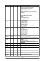
This command will turn off the front end cards for 4.0uSec. After the 4.0uSec the front end
cards will be turned on same as the original configuration of active front end card list as shown
in the figure
Timing Parameters
Figure 1.4 CONFGFEC- Chronogram.
43
EXESEQExecute Sequence (Start Sequencer)
Instruction Code
0x5304
Access Type
Command
Description
This command will start the execution of Instruction sequencer. Instruction sequencer will execute
the sequence loaded in the instruction memory.
44
ABRTSEQ
Abort Sequence (Stop Sequencer)
Instruction Code
0x5305
Access Type
Command
Description
This command will abort the execution of current sequence which is being executed by the
sequencer. Instruction sequencer will exit from the sequence loaded in the instruction memory
to idle state.
45
SWTTRGSoftware Trigger
Instruction Code
0x5306
Access Type
Command
Description
This command will issue sequence of L1a and L2a to front end cards. The latency between
L1 and L2 is programmable through the Altro interface configuration register (ALTROIF).
Timing Parameters
Latency between L1 and L2 is programmable with Altro interface register. Total of 13 bits can
be assigned to set this latency. L1 is synchronized with respect to sampling clock asserted for
two clock cycle. Similar way L2 to FEC is synchronized with read out clock as shown in figure
1.4
Figure 1.5 software trigger chronogram.
46
CLRERSTREGClear Error and Status Registers
Instruction Code
0x5307
Access Type
Command
Description
This command clears all the error status registers. The coding of this command from DDL is
different. DDL send command function is used to issue this command and value passed to
the function must be (0x10000)
47
CLRCNTClear Error and Status Registers
Instruction Code
0x5309
Access Type
Command
Description
This command clears all the counters in the RCU.
48
ARM_SYNCHArm Synchronization of Sampling Clock
Instruction Code
0x530A
Access Type
Command
Description
This command will set the RCU for Synchronization with L0 of SOD. Sampling Clock is reset
upon receiving the first L0 after this command has been received.
49
Chapter
1B
2
RCU Data Format
In the RCU, the 40-bit wide ALTRO data packets are formatted into 32-bit wide packet.
Structure of event data is described in table 1.26 The 32-bit data packet is completed by a
trailer (table 1.1) to form the RCU data block. The trailer consists of 2 fixed words, the first and
the last one in the trailer, and N optional words that carry information on the settings and
status of the FECs and RCU.
The two fixed trailer words define respectively: 1) the Payload Length, which specifies the
number of 40-bit data words; 2) the RCU Address and the Trailer Length in 32-bit words.
The optional words that compose the trailer consist of a parameter code (the 6 MSB), and the
parameter itself that consists of 26 bits. The parameters to be appended to the Event Trailer
will be stored in a dedicated RCU memory (Trailer Memory) that contains a maximum of 64
words. The actual number of parameter that will be included in the Trailer is variable and is
defined by the first word in the Trailer Memory. Hereunder, detail of each parameter is
described in table 1.32, that will be included in the RCU Firmware V2.0).
Common Data Header (8 words)
Payload (Variable nr. of words, minimum 0)
RCU Trailer (9 words)
Table 1.31 Structure of the Event data block
50
9B
2.1 Common Data Header (CDH)
The various fields of the common data format header are either loaded using the data
transmitted by the ALICE Trigger system or created locally by the RCU when running without
the ALICE Trigger system (e.g. for standalone tests). The parameters which are set at the
RCU level are described here.
Table 2.1 Common Data Header
Block Length parameter in CDH 0 is set to “FFFFFFFF”
RCU Version is set in CDH3 [31:24] set to “0X2”
In CHD4 status & Error bits are set by RCU. RCU receives total of 25 bits of errors from trigger receiver
module and code them into these 15 bits. These errors are described in table 2.2.
51
Error Bit
No
0
1
2
3
4
5
6
7
8
9
10
11
12
Name
Spurious L0
Missing L0
0
0
Incomplete L1
Message
Incomplete L2a
Message
Incomplete RoI
Message
L1 message
missing/timeout
L2 message
arrives outside
legal timeslot
RoI message
missing/timeout
0
0
0
0
TTCrx Address
Error
L2 message
arrives outside
legal timeslot
L2 message
missing/timeout
Prepulse error
Serial B Stop Bit
Error
SingleBit Hamming
Error Individually
Addr
Double Bit
Hamming Error
Individually Addr
Double Bit
Hamming Error
Broadcast
Unknown Message
Address Received
TTCrx Address
Error
L1 message
arrives outside
legal timeslot
L2 message
arrives outside
legal timeslot
RoI message
Explanation
High if a L0 trigger comes outside of the legal time window for a
L0.
High if the L0 trigger is missing
Data parity error: Not handled in RCU set to ‘0’
Control parity error : Not handled in RCU set to ‘0’
High when less than 4 L1 data words follows a L1 header
High when less than 7 L2a data words follows a L2a header
High when less than 3 RoI data words follows a RoI header
High if the L1 message does not start to arrive within the legal
time window for a L1 message.
High if all or part of the L2a/L2r message arrives outside of the
legal time window for a L2a/L2r message.
High if the RoI message does not start to arrive within the legal
time window for a RoI message.
Front-end electronics error Not Handled in RCU set to ‘0’
HLT decision flag : Not Handled in RCU set to ‘0’
HLT payload flag: Not Handled in RCU set to ‘0’
DDG payload flag: Not Handled in RCU set to ‘0’
High if the TTCrx address is unequal to 0x8001. The message
will not be decoded if this is this case and the message decoder
will return to idle.
High if all or part of the L2a/L2r message arrives outside of the
legal time window for a L2a/L2r message.
High if the L2a/L2r message does not start to arrive within the
legal time window for a L2a/L2r message
Not Used.
Serial B stop bit is 0 when it is expected to be 1
Single bit hamming error found and corrected in individually
addressed message.
Double bit hamming error found in individually addressed
message, not possible to correct. Most likely a lot of other errors
will come as a result of this.
Double bit hamming error found in broadcast message, not
possible to correct. Most likely a lot of other errors will come as
a result of this.
If an individually addressed message has arrived with a not
known address. Known addresses are given in Table 5-7.
High if the TTCrx address is unequal to 0x8001. The message
will not be decoded if this is this case and the message decoder
will return to idle.
High if all or part of the L1 message arrives outside of the legal
time window for a L1 message.
High if all or part of the L2a/L2r message arrives outside of the
legal time window for a L2a/L2r message.
High if all or part of the RoI message arrives outside of the legal
52
arrives outside
legal timeslot
RoI message
missing/timeout
L1 message
content error
L2 message
content error
13
14
15
RoI message
content error
Missing L1
0
0
time window for a RoI message.
High if the RoI message does not start to arrive within the legal
time window for a RoI message.
High if a combination of the following occur:
CIT_L1 = 0 after arrival of pre-pulse
L1_SwC = 0 when CIT_L1 = 1
L1_SwC /= L2_SwC
CIT_L1 /= CIT_L2a
ESR_L1 /= ESR_L2a
High if a combination of the following occur:
BCID_L2a/L2r > 3563
CIT_L2 = 0 after arrival of pre-pulse
L2_SwC = 0 when CIT_L2 = 1
L1_SwC /= L2_SwC
CIT_L1 /= CIT_L2a
ESR_L1 /= ESR_L2a
High if a combination of the following occur:
BCID_RoI > 3563
High if the L1 trigger is missing
Multi-event buffer error: Not Handled in RCU set to ‘0’
Reserved (Not used) ‘0’
Table 2.2 Error & Status Bit in CDH 4 [27:12]
53
2.2 Pay Load (ALTRO Read out Data)
10B
ALTRO data is sent in 32 bit format from RCU to DDL. Each 32 bit word consists of three 10 bit
words. The data is sent from RCU to DDL in LIFO manner (reverse order) as it is received from FEC.
Order of 10 bit words in 32 bit data packet is shown in table 2.3
31 30 29
20 19
01 E
10 9
0
Altro channel header 1
00
DW9
DW8
DW7
00
DW6
DW5
DW4
00
DW3
DW2
DW1
00
DW0
0x00
0x00
01 E
Altro channel header 2
00
DW4
DW3
DW2
00
DW1
DW2
0x00
01 E
00
Altro channel header 3
DW3
DW2
DW1
Table 2.3 Order of 10 bit words in 32 bit data packet
Altro channel header [11:0]: [Channel Address from Altro]
Altro channel header [25:16]: [Block Length Number of 10 bit words from Altro]
Altro channel header [29]: E: Channel Error Bit, it is set to “1” if there has been a mismatch for channel
address or block length received from ALTRO trailer. RCU will add a corrected Altro channel header
followed by the data received from corresponding channel.
Altro channel header [31:30]: Word ID = “01” to mark ALTRAO Header : “00” for payload
Altro channel header [15:12] – [28:26]: Reserved = “0000”
DW: 10 bit data word.
0x00: Padding
54
2.3 RCU Trailer
11B
Event data is followed by RCU trailer. This trailer comprises of 9 words of 32 bits. Start and end of
RCU trailer is marked by two most significant bits. Each trailer word consists of parameter code and its
value. RCU trailer format is shown in table 2.4. detail of each parameter is described as followed.
31
30 29
Word ID
26 25
0
Parameter
Value
10
Pay Load Length
0000
Number of 32 bit words
10
Error Register 1
0001
Error Registers for Branch A and B
10
Error Register 2
0010
Read out Errors
10
Error Register 3
0011
Number of Altro Trailer Errors
10
Act FEC A
0100
Active Front End Cards for Branch A
10
Act FEC B
0101
Active Front End Cards for Branch B
10
RDO CONFIG 1
0110
Readout configuration Register1 of Altro
10
RDO CONFIG 2
0111
Readout configuration Register2 of Altro
11
RCU ID
1000
RCU
FW
version
RCU address
Table 2.4 RCU Trailer
[31:30]: Word ID: two most significant bits are used to identify the start and end of RCU trailer.
Word ID= “10” shows that the word belong to RCU Trailer where as “11” shows that this is the last word of
the RCU trailer.
[29:26]: Parameter: four bits field is used to mark different words in the RCU trailer
[25:0]: Value: These 26 bits are used to record the status of the parameters listed in the table for
the event.
55
Pay Load lengthNumber of 32 bit words transmitted from RCU
Word ID
Parameter Code
Value
10
0000
Number of 32 bit words
Description
This trailer words contains the number of data words sent from RCU to SIU. It’s the first word in trailer and
the parameter code is 0x0. The Word ID is two most significant bits set to “10” showing that the word is part
of RCU trailer.
56
Error Register 1Error Register from Branch A and Branch B
Word ID
Parameter Code
Value
10
0001
Error Registers for Branch A and B
Description
This trailer words contains information about errors occurred during normal read / write / command
operation on FEC for branch A and branch B. Mapping of these bit with respect to branches is described
below.
Error Register1 [25:13] = FECERRA[19 :7];
Error Register1[12:0] = FECERRB[19 :7];
FECERRA and FECERRB are two status registers, copy of these registers are mapped in this trailer word.
List of the errors in FEC ERRA and FEC ERRB and respective bits are given as under.
FECERR[18]: ALTRO error signal asserted while data being transferred;
FECERR[17]:transfer not asserted;
FECERR[16]: ALTRO error asserted before transfer;
FECERR[15]: Write FSM error when started by RDO FSM;
FECERR[14]: ackn not released by ALTRO;
FECERR[13]: ALTRO error asserted while waiting for ackn to be released;
FECERR[12]: ALTRO does not assert ackn;
FECERR[11]: ALTRO error asserted while waiting for ackn;
FECERR[10]: ALTRO asserts ackn before assertion of cstb;
FECERR[09]: ALTRO error asserted while waiting for ackn in state “chkack”;
FECERR[08]: ALTRO error asserted in state “assertbus”
FECERR[07]: ALTRO error asserted in the execution of a broadcast command
57
Error Register 2Readout Errors
Word ID
Parameter Code
Value
10
0010
Read out Error Register
Description
This trailer words contains the errors occurred during readout process. Bit number 7 and 8 shows that
there has been at least one channel address or block length mismatch in the event data.
SCANEVENLEN error and EVLENRDO errors are related to the errors occurred during sparse readout.
ERR_REG2[8] :
Block Length mismatch
ERR_REG2[7]:
Channel Address mismatch;
ERR_REG2[6]:
RDYRX error;
ERR_REG2[5]:
SCANEVLEN error;
ERR_REG2[4:0]:
EVLENRDO error;
58
Error Register 3Number of Altro Trailers Errors
Word ID
Parameter Code
Value
10
0011
Count address & block length mismatch
Description
This trailer words contains the number of channel address and block length mismatches found in the
trailers sent from Altro. Channel address mismatch is incremented when the last channel addressed
is different than the channel address in Altro trailer. block length mismatch is marked by comparing
the number of data strobes and number of 10 bit words in the Altro trailer.
ERR_REG3 [11:0] = Number of mismatches in the channels address detected by the data
assembler during the readout
ERR_REG3[24:12] = Number of mismatches in the channel data block length detected by the data
assembler during the readout
59
Act FEC AActive Front End Card List for Branch A
Word ID
Parameter Code
Value
10
0100
Active Front End Cards on Branch A
Description
This trailer words contains the of Active Front End Cards(FECs) in branch A. This information
is copied same as configured during RCU configuration for readout. The Word ID is two most
significant bits set to “10” showing that the word is part of RCU trailer.
60
Act FEC BActive Front End Card List for Branch B
Word ID
Parameter Code
Value
10
0101
Active Front End Cards on Branch B
Description
This trailer words contains the list of Active Front End Cards (FECs) in branch B. This
information is copied same as configured during RCU configuration for readout. The Word ID
is two most significant bits set to “10” showing that the word is part of RCU trailer where as the
parameter code is 0101.
61
RDO CONFIG 1Read out Configuration 1(Copy of ALTRO Register DPCFG 1)
Word ID
Parameter Code
Value
10
0110
Copy of ALTRO Register
Data Path Configuration 1
Description
This trailer words is copy of Altro Register DPCFG 1 for TPC application for details please see
ALTRO manual page 36, 37. This register can be written as ALTROCFG1 at 0x5104. This
register can be configured for any detector related information please consult page 13 of this
manual.
62
RDO CONFIG 2Read out Configuration 2 (Copy of ALTRO Register DPCFG 2)
Word ID
Parameter Code
Value
10
0111
Copy of ALTRO Register
Data Path Configuration 2
Description
This trailer words is copy of Altro Register DPCFG 2 for TPC application for details please see
ALTRO manual page 36, 37. This register can be written as ALTROCFG2 at 0x5105. This
register can be configured for any detector related information please consult page 14 of this
manual.
[4 :0] Phase of sampling clock with respect to Arrival of the trigger
63
RCU IDRCU Identification Register
Word ID
Parameter Code
Value
11
1000
RCU Identification
Description
This trailer words contains the parameters related to the RCU in terms of its location. This
parameter contains the firmware version as well. Details of the this parameter is given as
under:[25:16] = 0x2 RCU Firmware Version;
[15:7] = RCU Address
RCU Address [8] = 0 for A-side, 1 for C-side
RCU Address [7:3] = sector number (0:17)
RCU Address [2:0] = readout partition number (0:5)
[6:0] = Trailer length (no. of 32-bit words related to trailer words)
64
Chapter
1B
3
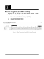
Monitoring Unit (SLOW Control)
Monitoring unit can read all of the status registers available in board
controller. Read process is done in three steps:i)
Write address in the SC Address Register (0x8005)
ii)
Give Execute Command 0x8010
iii)
Read the result Register 0x8002
Figure 3.1 Read Transaction from MSM to Board Controller
65
Appendix
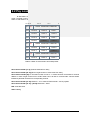
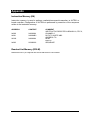
Instruction Memory (IM)
Instruction memory is used to perform read/write/command transaction to ALTRO or
board controller. Configuration of ALTROs is performed by execution of the sequence
written in the instruction memory.
ADDRESS
CONTENT
0x000
0x001
0x20000A
0x000ABC
0X002
0x00000A
0x003
0X380000
COMMENT
WRITE ALTRO REGISTER A BRANCH A, FEC 0 ,
CHANNEL 0
DATA TO WRITE:ABC
ADDRESS TO
READ
END OF
SEQUENCE
Readout List Memory (ROLM)
Readout list memory is configured with channel addresses for event readout.
66
67