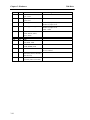
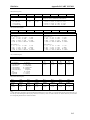
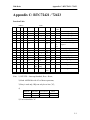
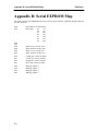
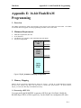
1
i386-Drive™
C/C++ programmable, 32-bit microprocessor module with
70+ I/Os, UARTs, ADC, DAC, and quadrature decoders
based on the Intel386EX
Technical Manual
1724 Picasso Avenue, Suite A, Davis, CA 95616-0547, USA
Tel: 530-758-0180
Fax: 530-758-0181
Internet Email: [email protected]
http://www.tern.com
COPYRIGHT
i386-Drive, i386-Engine, i386-Engine-P, MemCard-A, NT-Kit, and ACTF are trademarks
of TERN, Inc.
Intel386EX and Intel386SX are trademarks of Intel Corporation.
Borland C/C++ is a trademark of Borland International.
Microsoft, MS-DOS, Windows, Windows95, and Windows98 are trademarks of
Microsoft Corporation.
IBM is a trademark of International Business Machines Corporation.
Version 2.02
August 13, 1999
No part of this document may be copied or reproduced in any form or by any means
without the prior written consent of TERN, Inc.
© 1999
1724 Picasso Avenue, Suite A, Davis, CA 95616-0547, USA
Tel: 530-758-0180 Fax: 530-758-0181
Internet Email: [email protected]
http://www.tern.com
Important Notice
TERN is developing complex, high technology integration systems. These systems are
integrated with software and hardware that are not 100% defect free. TERN products are
not designed, intended, authorized, or warranted to be suitable for use in life-support
applications, devices, or systems, or in other critical applications. TERN and the Buyer
agree that TERN will not be liable for incidental or consequential damages arising from
the use of TERN products. It is the Buyer's responsibility to protect life and property
against incidental failure.
TERN reserves the right to make changes and improvements to its products
without providing notice.
i386-Drive
Table of Contents
Table of Contents
Chapter
page
1. Introduction ..................................................1-1
1.1 Functional Description ..........................1-1
1.2 Features .................................................1-2
1.3 Physical Description ..............................1-3
1.4 i386-Drive Programming Overview........1-4
1.4.1 Step 1.............................................1-5
1.4.1 Step 2.............................................1-6
1.4.1 Step 3.............................................1-6
1.5 Minimum Requirements ........................1-7
1.5.1 Minimum Hardware Requirements.1-7
1.5.2 Minimum Software Requirements ..1-7
2. Installation ...................................................2-1
2.1 Software Installation ..............................2-1
2.2 Hardware Installation ............................2-1
2.2.1 Connecting the i386-Drive to
the PC .............................................2-2
2.2.2 Powering-on the i386-Drive ..........2-3
3. Hardware ......................................................3-1
3.1 Intel386EX Processor ............................3-1
3.2 Intel386EX I/O Lines ............................3-1
3.3 External Interrupts and Schmitt-Trigger
Input Buffer ............................................3-3
3.4 Timer Control Unit................................3-4
3.5 Clock.....................................................3-4
3.6 Serial Ports............................................3-4
3.7 Power-Save Mode ..................................3-5
3.8 Memory Map for RAM/ROM .................3-5
3.9 I/O Mapped Devices ..............................3-6
3.9.1 I/O Space ......................................3-6
3.9.2 Programmable Peripheral Interface
(82C55A).........................................3-7
3.9.3 Real-time Clock RTC72423............3-9
3.9.4 UART SCC2691 ............................3-9
3.9.5 UART SCC2692 ............................3-9
3.10 Other Devices.......................................3-9
3.10.1 On-board Supervisor with
Watchdog Timer ..............................3-9
3.10.2 EEPROM ...................................3-10
3.10.3 12-bit ADC, TLC2543 ...............3-11
3.10.4 24-bit ADC, LTC2400 ...............3-11
3.10.5 100 KHz 16-bit ADC, LTC1605 3-11
Chapter
page
3.10.6 Dual 12-bit DAC, LTC1446 ...... 3-12
3.10.7 Parallel 12-bit DAC, LTC1450 . 3-12
3.10.8 16-bit DAC, LTC1655 .............. 3-12
3.10.9 HCTL2020 ................................ 3-12
3.11 Headers and Connectors..................... 3-13
3.11.1 Expansion Headers J1 and J2 ..... 3-13
3.11.2 Expansion Headers P1 and P2.... 3-15
3.11.3 Jumpers and Headers ................. 3-15
4. Software ....................................................... 4-1
4.1 IE.LIB .................................................. 4-2
4.2 Functions in IE.OBJ .............................. 4-2
4.2.1 i386-Drive Initialization ................ 4-2
4.2.2 External Interrupt Initialization ..... 4-4
4.2.3 I/O Initialization ............................ 4-5
4.2.4 Analog-to-Digital Conversion ....... 4-6
4.2.5 Digital-to-Analog Conversion ........ 4-7
4.2.6 Other Library Functions................. 4-7
4.3 Functions in SER0.OBJ/SER1.OBJ ....... 4-9
4.4 Functions in SCC.OBJ ........................ 4-14
4.5 Functions in IEEE.OBJ ....................... 4-16
Appendices:
A. i386-Drive Layout ................................ A-1
B. UART SCC2691 ...................................B-1
C. RTC72421/72423 ................................ C-1
D. Serial EEPROM Map .......................... D-1
Schematics:
i386-Drive (sheets 1 and 2)
i
i386-Drive
Chapter 1: Introduction
Chapter 1: Introduction
1.1 Functional Description
The i386-Drive (ID) is a compact, low-cost, high performance controller based on the 33 MHz, 32-bit
Intel386EX. It combines the powerful i386EX CPU and numerous peripherals on a single PCB measuring
4.7 by 4.5 inches.
The ID supports up to 512 KB 8-bit SRAM, 512 KB 8-bit Flash, 1 MB 16-bit SRAM, and 1 MB 16-bit
Flash. A 512-byte serial EEPROM, which does not require a battery backup, can be used as an additional
memory device to store important data. An optional real-time clock (RTC) provides information on the
year, month, date, hour, minute, second, 1/64 second. A lithium coin battery can be installed to back up
both the SRAM and RTC.
ROM/FLASH
8-bit SRAM
16-bit SRAM
16-bit FLASH
512 KB
512 K B
512 KB x 2
1MB 29F800
A8-A25
ADC U14
100KHz 16-bit
ADC U21
24-bit
ADC U010
11 Ch. 12-bit
ADC U011
11 Ch. 12-bit
691 U6
HP2020U08
HP2020U06
512-BYTE
DAC U09
DAC U24
100KHz 12-bit
16-bit
D0-D7
A0-A7
U5
EEPROM
RTC
Intel386EX
CPU
33 MHz
U4
DAC U23
2 ch. 12-bit
DMA (2)
16-Bit Timers (3)
Ext. Interrupts (10)
8x3 I/O lines
UART
U8
SCC2961
SIO0
SIO1
SSIO
UART U04
SCC2962
P1
32x2
P2
32x2
J8
& J7
18x1
H2
SER0 RS232
J1
20x2
H3
SER1 RS232
PIO, TXD
24 I/O PPI
U01
82C55
J2
20x2
24 I/O PPI
H4 SCC2691
H1 SCC2692A
H5 SCC2692B
U02
82C55
Figure 1.1 Functional block diagram of the i386-Drive
Two asynchronous serial ports from the i386EX support reliable DMA-driven serial communication at up
to 115,200 baud with RS-232 drivers. The i386EX also offers one synchronous serial port. An optional
UART SCC2691 and a dual UART SCC2692 can be added for an additional three asynchronous serial
ports with RS-232 or RS-485 drivers.
Three PC-compatible 16-bit programmable timers/counters can generate interrupts or count external
events, at a rate of up to 8 MHz, or can generate pulse outputs. Three 8-bit, multifunctional, userprogrammable I/O ports are included in the i386EX. Four external interrupts are buffered by Schmitttrigger inverters and provide active low inputs. A supervisor chip (LTC691) with a watchdog timer is onboard.
Two PPI chips (82C55) provide 48 user-programmable I/O lines totally free for application use. The
optional SCC2692 UART provides 15 additional I/O lines.
The ID supports many optional ADC and DACs. Up to 22 channels of 12-bit ADC (LTC2543, 0-5V, 10
KHz), one 16-bit ADC (LTC1605, ±10V, 100 KHz), and one 24-bit ADC (LTC2400, 0-5V, 5 Hz) can be
1-1
Chapter 1: Introduction
i386-Drive
installed. Two 12-bit DACs (LTC1446, 0-4.095V, 10 KHz), one 100 KHz 12-bit DAC (LTC1450,
0-4.095V), and one 16-bit DAC (LTC1655, 0-4.095V, 10 KHz) are available.
Two quadrature decoders (HP2020) can interface to optical encoders for motion control. Schmitt-trigger
inverters are provided.
On-board expansion headers provide data lines, address lines, control signals, and pre-decoded chip select
lines.
By default, a 5V switching regulator (up to 35V DC input) is installed to reduce power consumption and
heat. The switching regulator introduces more noise than a linear regulator: a linear regulator can be
installed upon request.
In “power-off” mode, the ID consumes very low (µA) power. Users can turn off the switching regulator
via software, and use the RTC or an external signal to turn it on.
A MemCard-A can be installed on the ID to provide an additional 33 12-bit ADC, 6 24-bit ADC, 420 MB
PCMCIA memory, and an Ethernet interface.
Figure 1.2 An i386-Drive with a MemCard-A installed
1.2 Features
Standard Features:
•
•
•
•
•
•
•
•
•
•
•
1-2
Dimensions:
4.7 x 4.5 x 0.6 inches
Easy to program in C/C++
Power consumption: 300/160/80/30 mA at 8.5/12/24/35V
Power input:
+8.5 to +35 V
Temperature range:
-40°C to +80°C
32-bit CPU (Intel i386EX, 33 MHz), C/C++ programmable
24 multiplexed I/Os
interrupts, DMA
512-byte serial EEPROM
48 bi-directional I/O lines from 2 PPIs
Up to 3 MB SRAM/Flash supported
i386-Drive
•
•
Chapter 1: Introduction
2 asynchronous serial ports with RS-232 drivers, 1 synchronous serial port
Supervisor chip (691) for power failure, reset and watchdog
Optional Features (* surface-mounted components):
•
•
•
•
•
•
•
•
•
•
•
•
•
32KB, 128KB, or 512KB 8-bit SRAM*
256KB or 1 MB 16-bit SRAM*
512KB or 1MB 16-bit Flash*
up to 22 channels of 12-bit ADC, sample rate up to 10 KHz*
16-bit ADC (LTC1605, ±10V, 100 KHz)*
24-bit ADC (LTC2400, 0-5V, 5 Hz)*
2 channels of 12-bit DAC, 0-4.095V output*
100 KHz 12-bit DAC (LTC1450, 0-4.095V)*
16-bit DAC (LTC1655, 0-4.095V, 10 KHz)*
SCC2691 UART (on-board) supports 8-bit or 9-bit networking, with RS-232* or RS-485 drivers
SCC2692 dual UART, with RS-232* or RS-485 drivers
up to 2 quadrature decoders (HP2020)
Real-time clock RTC72423*, lithium coin battery*
1.3 Physical Description
The physical layout of the i386-Drive is shown in Figure 1.3.
P2
H1
H5
H2
U012
232/
485
U013
232
U16
2400 U21
H4
485
U19
232/
485
U20
U014
SCC2692
PPI
U04
U02
LTC
1450
H3
U09
LTC1605
U14
J7
J8
J5
J1
U3
U1
U4
U8
U18
UART
ROM/
Flash
16-bit SRAM
U05
HC138
16-bit SRAM
U15
U2
HC14
K1
U06
HP2020
U08
PPI
HC14
U01
J0
U5 EE
U7
HP2020
H0
HC259
U10
U13
Flash
29Fx00
66 MHz
J2
U17
691
U6
U23
U24
1446
1655
2543
2543
U011
U010
PAL
i386
H7
J4
8-bit SRAM
H10
J3
RTC
I1
U9
U07
P1
Figure 1.3 Physical layout of the i386-Drive
1-3
Chapter 1: Introduction
i386-Drive
1.4 i386-Drive Programming Overview
Development of application software for the i386-Drive consists of three easy steps, as shown in the block
diagram below.
STEP 1 Serial link PC and i386-Drive, program in C/C++
Debug C/C++ program on the i386-Drive with Remote Debugger
STEP 2
Test i386-Drive in the field, away from PC
Application program resides in the battery-backed SRAM
STEP 3
Make application ROM or Download to Flash
Replace DEBUG ROM, project is complete
You can program the i386-Drive from your PC via serial link with an RS232 interface. Your C/C++
program can be remotely debugged over the serial link at a rate of 115,000 baud. The C/C++ Evaluation
Kit (EV) or Development Kit (DV) from TERN provides a Borland C/C++ compiler, TASM, LOC31,
Turbo Remote Debugger, I/O driver libraries, sample programs, and batch files. These kits also include a
DEBUG ROM (TDREM_i386EX) to communicate with Turbo Debugger, a PC-V25 cable to the connect
the controller to the PC, and a 9-volt wall transformer. See your Evaluation/Development Kit Technical
Manual for more information on these kits.
After you debug your program, you can test run the i386-Drive in the field, away from the PC, by
changing a single jumper, with the application program residing in the battery-backed SRAM. When the
field test is complete, application ROMs can be produced to replace the DEBUG ROM. The .HEX or .BIN
file can be easily generated with the makefile provided. You may also use the DV Kit or ACTF Kit to
download your application code to on-board Flash.
The three steps in the development of a C/C++ application program are explained in detail below.
1-4
i386-Drive
Chapter 1: Introduction
1.4.1 Step 1
STEP 1: Debugging
•
Write your C/C++ application program in C/C++.
•
Connect your controller to your PC via the PC-V25 serial link cable.
•
Use the batch file m.bat to compile, link, and locate, or use t.bat to compile, link locate,
download, and debug your C/C++ application program.
IDE10
H5
485
U01
J3
DB9
RTC
J4
J5
U1
i386
PC
J2
HC1
U2
PPI
U04
U02
U1
J1
U3
U8
U18
UART
RO
M/
16-bit
691
U6
66
MHz
K1
U1
HC1
Flash
29Fx0
0
U05
HC1
To COM1
or COM2
U0
U0
HP2020
U0
U0
H0
U EE
U2 U2
144 165
PPI
254
U01
DC
power
jack
U17
16-bit
HC2
U1
U
HP2020
U0
LTC160
J7
8-bit SRAM
U4
SCC2692
H
To H2
U01
232/
485
U01
232
U16
J8
240 U2
U19
232/
485
U20
U1
H2
H4
H1
H1
LTC
1450
P2
H
J0
PAL
RED edge of cable
connects to pin 1
of SER0 (H2)
254
U01
I1
U
P1
Wall transformer
+9V 500 mA
center negative
Figure 1.4 Step 1 connections for the i386-Drive
1-5
Chapter 1: Introduction
i386-Drive
1.4.2 Step 2
STEP 2: Standalone Field Test.
•
Set the jumper on J2 pins 38-40 on the i386-Drive (Figure 1.5).
•
At power-on or reset, if J2 pin 38 (RI1) is low, the CPU will run the code that resides in the batterybacked SRAM.
•
If a jumper is on J2 pins 38-40 at power-on or reset, the i386-Drive will operate in Step Two mode. If
the jumper is off J2 pins 38-40 at power-on or reset, the i386-Drive will operate in Step One mode.
The status of J2 pin 38 (signal RI1) of the Intel386EX is only checked at power-on or at reset.
P2
H1
H5
H2
U012
232/
485
U013
232
U16
2400 U21
H4
485
U19
232/
485
U20
U014
SCC2692
PPI
U04
U02
LTC
1450
H3
U09
LTC1605
U14
J7
J8
RTC
J5
J1
U3
8-bit SRAM
U8
U4
J2: pins 38=40
U18
UART
ROM/
Flash
16-bit SRAM
U05
HC138
16-bit SRAM
Flash
29Fx00
K1
PPI
HC14
U01
HP2020
U08
J0
U5 EE
U7
U06
U13
U10
U15
U2
HP2020
H0
HC259
66 MHz
J2
U17
691
U6
U23
U24
1446
1655
2543
2543
U011
U010
PAL
i386
HC14
(Note: Step2 jumper
should be off for
debugging in step 1)
U1
H7
J4
H10
Step 2 Jumper:
J3
I1
U9
U07
P1
Figure 1.5 Location of Step 2 jumper on the i386-Drive
1.4.3 Step 3
STEP 3: Generate the application .BIN or .HEX file, make production ROMs or download your program
to FLASH via ACTF.
•
If you are happy with your Step 2 test, you can go back to your PC to generate your application ROM
to replace the DEBUG ROM (TDREM_i386EX). You need to change DEBUG=1 to DEBUG=0 in the
makefile.
You need to have the DV Kit to complete Step 3.
Please refer to the Tutorial of the Technical Manual of the EV/DV Kit for further details on programming
the i386-Drive.
1-6
i386-Drive
Chapter 1: Introduction
1.5 Minimum Requirements for i386-Drive System Development
1.5.1 Minimum Hardware Requirements
•
•
•
•
PC or PC-compatible computer with serial COMx port that supports 115,200 baud
i386-Drive controller with DEBUG ROM TDREM_i386EX
PC-V25 serial cable (RS-232; DB9 connector for PC COM port and IDE 2x5 connector for controller)
center negative wall transformer (+9V 500 mA)
1.5.2 Minimum Software Requirements
• TERN EV/DV Kit installation diskettes
• PC software environment: DOS, Windows 3.1, Windows95, or Windows98
The C/C++ Evaluation Kit (EV) and C/C++ Development Kit (DV) are available from TERN. The EV
Kit is a limited-functionality version of the DV Kit. With the EV Kit, you can program and debug the
i386-Drive in Step Three and Step Two, but you cannot run Step Three. In order to generate an
application ROM/Flash file, make production version ROMs, and complete a project, you will need the
Development Kit (DV).
1-7
i386-Drive
Chapter 2: Installation
Chapter 2: Installation
2.1 Software Installation
Please refer to the Technical manual for the “C/C++ Development Kit and Evaluation Kit for TERN
Embedded Microcontrollers” for information on installing software.
The README.TXT file on the TERN EV/DV disk contains important information about the installation
and evaluation of TERN controllers.
2.2 Hardware Installation
Hardware installation for the i386-Drive consists primarily of connecting the microcontroller to your PC.
Overview
• Connect PC-V25 cable:
For debugging (STEP 1), place the 5x2 pin header on SER0 (H2)
with red edge of cable at pin 1 of H2
• Connect wall transformer:
Connect 9V wall transformer to power and plug into power jack
2-1
Chapter 2: Installation
i386-Drive
2.2.1 Connecting the i386-Drive to the PC
The following diagram (Figure 2.1) illustrates the connection between the i386-Drive and the PC. The
i386-Drive is linked to the PC via a serial cable (PC-V25).
The TDREM_i386EX DEBUG ROM communicates through SER0 by default. Install the 5x2 IDE
connector on the SER0 header (H2). IMPORTANT: Note that the red side of the cable must point to pin
1 of the H2 header. The DB9 connector should be connected to one of your PC's COM Ports (COM1 or
COM2).
SER0
U01
232/
485
U01
232
To H2
U16
J8
J3
RTC
J4
PC
Figure 2.1 Connecting the i386-Drive to the PC
U02
HC1
U2
HP2020
U0
U1
J1
U8
U18
16-bit
UART
ROM
/
691
U6
66
MHz
K1
U1
HC1
Flash
29Fx0
0
U05
P1
U0
U17
16-bit
H0
HC2
U1
U EE
U2 U2
144 165
PPI
U0
HP2020
U0
LTC160
U3
U
U0
2-2
J5
U1
J2
HC1
To COM1
or COM2
PPI
U04
J7
i386
Step2 jumper
should NOT
be installed
for debugging
240 U2
U19
232/
485
U20
SCC2692
8-bit SRAM
U4
H4
H
H2
485
U01
U1
DB9
H5
254
254
U01
U01
H1
H1
LTC
1450
P2
H
PAL
RED edge of cable
corresponds to pin 1
of SER0 header (H2)
(H2)
Pin 1
IDE10
I1
U
J0
i386-Drive
Chapter 2: Installation
2.2.2 Powering-on the i386-Drive
Connect a wall transformer +9V DC output to the DC power jack.
The on-board LED should blink twice and remain on after the i386-Drive is powered-on or reset, as
shown in Figure 2.2.
H5
485
U01
RTC
J4
J5
8-bit SRAM
U1
U4
HC1
U2
U1
J1
U3
U8
U18
UART
16-bit
691
U6
66
MHz
K1
U1
HC1
Flash
29Fx0
0
U05
HC1
U0
U0
U0
HP2020
U0
H0
U EE
U2 U2
144 165
PPI
254
U01
DC power jack
U17
16-bit
HC2
U1
U
HP2020
U0
LTC160
RO
M/
i386
J2
U02
J7
J8
J3
PPI
U04
U1
232
U16
SCC2692
H
U01
232/
485
U01
240 U2
U19
232/
485
U20
254
U01
H1
H2
H4
J0
PAL
H1
LTC
1450
P2
H
I1
U
P1
Red LED
Wall transformer
+9V 500 mA
center negative
Figure 2.2 The LED blinks twice after the i386-Drive is powered-on or reset
2-3
i386-Drive
Chapter 3: Hardware
Chapter 3: Hardware
3.1 Intel386EX Processor
The Intel386EX is based on the Intel386SX processor. This highly integrated device retains PC functions
that are useful in embedded applications and adds peripherals that are typically needed in embedded
systems. The Intel386EX has new peripherals and an on-chip system interface logic that can minimize
total system cost. The Intel386EX has two asynchronous serial ports, one synchronous serial port, 24 I/Os,
a watchdog timer, interrupt pins, three 16-bit timers, DMA to and from serial ports, and enhanced chipselect functionality. The i386-Drive provides a PC-compatible development platform optimized for
embedded applications.
3.2 Intel386EX I/O Lines
The Intel386EX has 24 I/O lines in three 8-bit I/O ports: P1, P2, and P3. The 24 I/O pins on the
Intel386EX are multiplexed with peripheral pin functions, such as serial ports, timer outputs, and chipselect lines. Each of these pins can be used as a user-programmable input or output signal if the normal
shared peripheral pin function is not needed. Any I/O line can be configured to operate as a highimpedance input, open-drain output, or complementary output.
After power-on or reset, the I/O pins default to various configurations. The initialization routine provided
by TERN libraries reconfigures some of these pins as needed for specific on-board usage as well. These
configurations, as well as the processor-internal peripheral usage configurations, are listed in Table 3.1.
PIO
P10
P11
P12
P13
P14
P15
P16
P17
P20
P21
P22
P23
P24
P25
P26
P27
P30
P31
P32
P33
P34
P35
P36
P37
Peripheral
DCD0#
RTS0#
DTR0#
DSR0#
RI0#
LOCK#
HOLD
HLDA
CS0#
CS1#
CS2#
CS3#
CS4#
RXD0
TXD0
CTS0#
TOUT0
TOUT1
INT0
INT1
INT2
INT3
PWDOWN
COMCLK
Power-On/Reset
weak pullup
weak pullup
weak pullup
weak pullup
weak pullup
weak pullup
Input with pulldown
Output with pulldown
Output with pullup
Output with pullup
Output with pullup
Output with pullup
Output with pullup
Input with pulldown
Output with pulldown
Input with pullup
Output with pulldown
Output with pulldown
Input with pulldown
Input with pulldown
Input with pulldown
Input with pulldown
Input with pulldown
Input with pulldown
i386-Drive Pin No.
J2 pin 14
J2 pin 27
J2 pin 18
J2 pin 20
J2 pin 12
EE U5.5&ADC U10.16
J2 pin 11
J2 pin 13
LT691 U6.13
J2 pin 37
J2 pin 5
J2 pin 10
J2 pin 3
J2 pin 32
J2 pin 34
J2 pin 36
J2 pin 17
J2 pin 19
J2 pin 21
J2 pin 23
J2 pin 24
J2 pin 29
J2 pin 30
J2 pin 35
i386-Drive Initial
Input with pullup
Output
Input with pullup
Input with pullup
Input with pullup
I/O with pullup
Input with pulldown
Input with pulldown
8-bit SRAM select
U15 Flash select
SCC & RTC I/O select
16-bit SRAM select
16-bit ADC/DAC select
RXD0
TXD0
Input with pullup
Input with pulldown
Input with pulldown
Input with pulldown
Input with pulldown
Input with pulldown
Input with pulldown
Input with pulldown
Input with pulldown
Table 3.1 I/O pin default configuration after power-on or reset
3-1
Chapter 3: Hardware
i386-Drive
The 24 PIO lines, P10-P17, P20-P27, and P30-P37 are configurable via 8-bit registers, PnDIR and
PnLTC. The value settings are listed as follows:
Pin Configuration
Desired Pin State
PnDIR
PnLTC
High-impedance input
high impedance
1
1
Open-drain output
0
1
0
Complementary Output
1
0
1
Complementary Output
0
0
0
Table 3.2 Value settings for PIO lines
TERN libraries can be used to manipulate these IO pins for you. C functions provided in the library
ie.lib and found in the header file ie.h can be used to initialize these PIO pins at run-time. Details
for these can be found in the Software chapter.
Some of the I/O lines are used by the i386-Drive system for on-board components (Table 3.3). We suggest
that you do not use these lines unless you are sure that you are not interfering with the operation of such
components (i.e., if the component is not installed).
Signal
Pin
Function
P21 = /CS1
P22 = /CS2
P23 = /CS3
P24 = /CS4
/CS5
RI1
P15
J2.37
J2.5
J2.10
J2.3
(N/A)
J2.38 and P2.3
U5.5
P20 = /CS0
P26 = TxD0
P25 = RxD0
DSR1
(N/A)
J2.34
J2.32
J2.4
DCD1
P30
/INT4
/INT5
/INT6
J2.1
J2.17
J2.33
J2.8
J2.6
16-bit Flash U15
8-bit I/O for U4 RTC, U8 SCC, PPIs, SCC2692, /HP1, /HP2
16-bit SRAM U17+U18
16-bit I/O for high speed ADC/DAC
U10 74HC259 chip for internal signals T0 to T7
STEP 2 jumper
EEPROM SDA = U010 pin 16 ADC DOUT
Shared with U010 TLC2543 ADC and U5 24C04 EE data input
The ADC and EE data output can be tri-state, while disabled.
U6.13 for SRAM chip select, base memory address 0x0000
SER0 transmit for default debug ROM
SER0 receive for default debug ROM
U011 TLC2543 ADC DOUT or U08 HCTL2020 U/D to i386EX
They cannot be used at the same time.
U06 HCTL2020 U/D to i386EX
Timer0 out as HCTL2020 clock
U14 16-bit ADC LTC1605 Busy
U8 SCC2691 UART interrupt
U04 SCC2692 DUAL UART interrupt
Table 3.3 Functions of reserved I/O lines on the i386-Drive
At reset, the internal PC/AT-compatible peripherals are mapped into DOS I/O space, of which only
1 Kbyte is used. The DEBUG ROM and ie_init() enables Expanded I/O space. The registers
associated with the integrated peripherals are mapped in the address range of 0f000 to 0f8ffh.
There are four additional external interrupt lines (/INT4, /INT5, /INT6, /INT7) which are not shared with
PIO pins. These active-low-only lines are all buffered by Schmitt-triggers. For further details regarding
these external interrupt pins, refer to the External Interrupt section below (3.3).
3-2
i386-Drive
Chapter 3: Hardware
The specifications for these I/O pins state that they can sink up to 8 mA.
If you need further details regarding the Input/Output Ports, please refer to Chapter 16 of the Intel386EX
Embedded Microprocessor User’s Manual.
3.3 External Interrupts and Schmitt-Trigger Input Buffer
There are 10 external interrupt inputs that the user can adapt for his/her own use.
The master interrupt controller 82C59A supports six ACTIVE HIGH pins on the header J2:
INT0 = P32 = J2.21, vector=0x41
INT1 = P33 = J2.23, vector=0x45
INT2 = P34 = J2.24, vector=0x46
INT3 = P35 = J2.29, vector=0x47, IR7 share with Spurious Interrupts
INT8 = P31 = J2.19, vector=0x43 share with SIO1
INT9 = P30 = J2.17, vector=0x44 share with SIO0
The slave interrupt controller 82C59A has six pins, ACTIVE LOW at J2 header:
/INT4 = J2.33, vector=0x48
/INT5 = J2.8, vector=0x49
/INT6 = J2.6, vector=0x4c
/INT7 = J2.15, vector=0x4e
The WDTOUT (Watchdog Timer) interrupt uses vector=0x4f, and the NMI (Non-Maskable Interrupt) at
pin J2.7 uses vector=0x2. The NMI interrupt can not be disabled by software, and is raised on a rising
edge. /INT5, J2 pin 8, is used by the on-board optional SCC2691 UART if installed. /INT6, J2 pin 6, is
used by the on-board optional SCC2692 Dual UART if installed.
You must provide a low-to-high (rising) edge to generate an interrupt for the ACTIVE HIGH interrupt
inputs and a high-to-low (falling) edge to generate an interrupt for the ACTIVE LOW interrupt inputs.
A spurious interrupt is defined as an interrupt that is "Not Valid." A spurious interrupt on any IR line
generates the same vector number as an IR7 request. The spurious interrupt, however, does not set the inservice bit for IR7. Therefore, an IR7 interrupt service routine must check the interrupt service routine
register to determine if the interrupt source is either a valid IR7 (the in-service bit is set) or a spurious
interrupt (the in-service bit is cleared).
Four external interrupt inputs, /INT4-7, are buffered by Schmitt-trigger inverters (U7) in order to increase
noise immunity and transform slowly-changing input signals to fast-changing and jitter-free signals.
3-3
Chapter 3: Hardware
i386-Drive
/INT4=J2.33
/INT5=J2.8
/INT6=J2.6
/INT7=J2.1
5
INT4 =U2.93
U7D
INT5 =U2.94
U7C
INT6 =U2.95
U77
INT7 =U2.96
U7A
5
Figure 3.1 External interrupt inputs
The i386-Drive uses vector interrupt functions to response to external interrupts. Please refer to the
Intel386EX User’s Manual for detailed information about interrupt vectors, and to the Software chapter of
this manual (Chapter 4) on how to associate these interrupt vectors with your own interrupt service
routine.
3.4 Timer Control Unit
The timer/counter unit has three 16-bit programmable counters: timer0, timer1, and timer2. They can be
driven by a pre-scaled value of the processor clock or by external timers. The counters support six
different operating modes. Only mode2 and mode3 are periodic modes, in which the counters are reloaded
with the user-selected count value when they reach terminal count. For details regarding the modes in
which the timers operate, please refer to Chapter 10 of the Intel386EX manual.
The timers provided can be used in several applications. They can be used to act as counters, generate
interrupts, and to output repeating pulses with user-specified widths.
Timers can generate pulse outputs at the J1/J2 headers:
Timer 0 output=TOUT0=P30=J2 pin 17 (Use for U06/U08 HCTL2020(s), if installed)
Timer 1 output=TOUT1=P31=J2 pin 19
Timer 2 output=TOUT2=J1 pin 4
Timers can use internal or external clock as clock inputs.
To count external events, the timer clock inputs are routed to the J2 headers:
Timer 0 clock in=/INT4=J2 pin 33
Timer 1 clock in=/INT6=J2 pin 6
Timer 2 clock in=TCLK2=J2 pin 9
These timers can be used to count or time external events.
To use the timers to generate interrupts, a few different options are available. Timer 1 has its output
signal, OUT1, connected to IR2 of the slave 82C59. The Timer 2 output, OUT2, is connected to IR3 of
the slave 82C59. The Timer 0 output, OUT0, is connected to IR0 of the master 82C59.
The maximum external pulses input rate is 8.25 MHz. Please see the sample program timer.c and
counter0.c in c:\tern\386\samples\ie for details regarding the timers, counters, and their
applications.
3-4
i386-Drive
Chapter 3: Hardware
3.5 Clock
With an on-board 66 MHz oscillator, the i386-Drive operates at 33 MHz system processor clock speed.
The 66 MHz clock signal is routed to a 4-pin header H1 pin 1, next to the oscillator. The processor clock
is used by serial ports and timers. The default SERCLK for serial ports is 16.5 MHz, and the default prescaled PSCLK for the timers is 16.5 MHz. The maximum timer output is 8.25 MHz. For details regarding
how to change the PSCLK pre-scale register, see the sample programs timer.c and counter0.c in
c:\tern\386\samples\ie.
3.6 Serial Ports
The i386-Drive can provide up to five asynchronous serial channels. Two are Intel386EX-internal: SER0,
SER1. One external UART SCC2691 can be installed underneath the ROM. One optional dual UART
SCC2692 can be installed. All of the UARTs can operate in full-duplex communication mode. SER0 and
SER1 use DMA for receiving and for interrupt-driven transmit. The UART SCC2691 and Dual UART
SCC2692 are interrupt-driven for both transmitting and receiving. For more information about the
external SCC2691/2 UARTs, refer to Appendix C and the datasheets from the IC manufacturer (Philips
Semiconductor, Sunnyvale, California, tel. 408-991-3737).
With the DEBUG ROM (TDREM_i386EX) installed, the internal serial port SER0 is used by the
i386-Drive for DEBUG programming with the PC. It uses 115,000 Baud rate, as default, for
programming. SER0 and SER1 can both be used in applications: the user can use SER0 to debug an
application program for SER1, and then convert the SER1 code to SER0, since they are identical. The
application programs can be combined and downloaded via SER0 in STEP1, and then run in STEP2.
Application programs can use both SER0 and SER1 at the same time, but it cannot be debugged over
SER0 at the same time.
Complete interrupt/DMA-driven software serial port drivers are included in the EV/DV Kit. Please refer
to Chapter 4 (Software) for more details regarding the implementation of the serial port drivers, as well as
their application.
3.7 Power-Save-Mode
The i386-Drive can serve as a high-performance processor module for applications that require low power
consumption. The power-save mode of the Intel386EX processor reduces power consumption and heat
dissipation, thereby extending battery life in portable systems. In power-save mode, operation of the CPU
and internal peripherals continues at a slower clock rate. When an interrupt occurs, it automatically
returns to its normal operating rate.
The RTC72423 on the i386-Drive has a VOFF signal routed to J1 pin 9 and H0. The VOFF is controlled
by the battery-backed RTC72423. It will be in tri-state for the external power-off and become active-low at
the programmed time interrupt. The user may use the VOFF line to control an external switching power
supply that turns the power supply on/off.
See the sample program poweroff.c in the c:\tern\386\samples\ie directory.
3.8 Memory Map for RAM/ROM
The Intel386EX supports a memory space of up to 64 MB with 26 address lines (A0-A25).
At power-on, the i386EX operates in Real-mode, which offers only 1 MB of memory space using
segmentation. The DEBUG ROM operates in Real-mode as well, and does not use A20-A25.
3-5
Chapter 3: Hardware
i386-Drive
The lower memory chip select /CS0 is mapped into memory space of 0x00000 to 0x7ffff. This is used for
up to 512K of 8-bit SRAM, U1. The default wait state on the RAM is set to 3 cycles, but can be shortened
if desired.
The upper memory chip select /UCS is mapped into memory space of 0x80000 to 0xfffff and is used for up
to 512K of 8-bit ROM, U3. The U3 ROM socket supports both 8-bit ROM and 8-bit Flash chips. The
default wait state for this component is two cycles, to allow use with ROM components with speeds of up
to 120 ns. The preferred ROM speed is 70 ns, and if your environment is relatively noise free you can
reduce the wait state to one cycle using this component.
For details regarding how these components are initialized in ie_init() with these specifications,
please refer to the chapter on Software in the i386-Engine technical manual.
In certain applications, you might also choose to re-map the memory address space differently to other
chip select lines. An optional 16-bit FLASH (29F400, U15) can be installed. The default setting uses
P21=/CS1 as chip select. See the sample program id_f.c in the c:\tern\386\samples\id directory.
Two optional 8-bit SRAM chips can be installed in U17 and U18 to form up to 1MB 16-bit SRAM for the
i386EX, using P23=/CS3 as chip select.
See the sample file id_ram.c in the c:\tern\386\samples\id directory.
During development, your code and data segments will be mapped to specific locations within this
memory space. Details regarding how this is done during product development can be found in the
Technical Manual of the C/C++ EV/DV Software Kit.
3.9 I/O Mapped Devices
3.9.1 I/O Space
External I/O devices can use I/O mapping for access. You can access such I/O devices with inportb(port)
or outportb(port,dat). These functions will transfer one byte of data to the specified I/O address.
The external I/O space size is 64KB, ranging from 0x0000 to 0xffff.
The default I/O access time is 15 wait states. You may modify the wait states by re-programming the
Chip-select Low Address register from 0-15 cycles. The system clock speed is 33 MHz. Details regarding
this can be found in the Software chapter, and in the Intel386EX Embedded Microprocessor User’s
Manual. Slower components, such as most LCD interfaces, might find the maximum programmable wait
state of 15 cycles still insufficient.
For details regarding the chip select unit, please see Chapter 14 of the Intel386EX Embedded
Microprocessor User’s Manual.
The table below shows more information about I/O mapping:
3-6
I/O space
Select Signal
Location
Usage
0x8000-0x80ff
0xa000-0xa001
0xa002-0xa003
0xa004-0xa005
0xa006-0xa007
0xa080-0xa08f
0xa090-0xa09f
0xa0a0-0xa0af
0xa0b0-0xa0bf
/CS6
/CS2
/CS2
/CS2
/CS2
/CS2
/CS2
/CS2
/CS2
J1 pin 19 = /CS6
J2 pin 5 = P22
J2 pin 5 = P22
J2 pin 5 = P22
J2 pin 5 = P22
J2 pin 5 = P22
J2 pin 5 = P22
J2 pin 5 = P22
J2 pin 5 = P22
User or MemCard-A
Select U06 HP2020-1
Select U08 HP2020-2
RST1 for U06 HP2020-1
RST2 for U06 HP2020-2
/LD for DAC U09 LTC1450
UART, SCC2691
RTC 72423
/S1 for PPI1
i386-Drive
Chapter 3: Hardware
I/O space
Select Signal
Location
Usage
0xa0c0-0xa0cf
0xa0e0-0xa0ef
0xa0f0-0xa0ff
0xb000-0xb0ff
Not mapped
0x????
0x????
0xc000
/CS2
/CS2
/CS2
/CS5
/CS0
/CS1
/CS3
/CS4
J2 pin 5 = P22
J2 pin 5 = P22
J2 pin 5 = P22
None (U9-74HC259)
N/A
J2 pin 37 = P21
J2 pin 10 = P23
J2 pin 3 = P24
/S2 for PPI2
/S4 for SCC2692
/CLR for DAC U09 LTC1450
Internal Usage (T0-T7)
SRAM
16-bit Flash U15
16-bit SRAM, U17 and U18
Read/write 16-bit ADC/DAC
A total of eight pre-decoded chip-select lines are available on the ID. These include the UCS (upper chip
select), and signals CS0-6. The upper chip select is dedicated for boot-up ROM use.
The pre-decoded chip select lines listed in the table above can be used for application, if the on-board
optional corresponding device is not installed.
To use one of the chip select lines, you must map the appropriate line to a free base I/O address. After
configuring the PIO pin appropriately for this peripheral function (normal-mode operation), you can
directly outport to that address with appropriate data. The address bus and data bus should then be
connected to your I/O component if needed.
To illustrate how to interface the i386-Drive with external I/O boards, a simple decoding circuit for
interfacing to an external 82C55 I/O chip is shown in Figure 3.2.
82C55
74HC138
A4
A5
A6
1
2
3
/CS6=J1.19
A7
4
5
6
A
B
C
G2A
G2B
G1
Y0
Y1
Y2
Y3
Y4
Y5
Y6
Y7
15
14
13
12
11
10
9
7
RST
SEL8080
/SEL8090
/SEL80A0
/SEL80B0
/SEL80C0
/SEL80D0
/SEL80E0
/SEL80F0
P00-P07
A0/BLE
A1
/SEL8090
/CS
/WR
/WR
/RD
/RD
D0-D7
P10-P17
P20-P27
Figure 3.2 Interface i386-Drive to external I/O devices
The function ie_init() by default initializes the /CS6 line at base I/O address starting at 0x8000. You
can read from the 82C55 with inportb(0x8090) or write to the 82C55 with outportb(0x8090,dat). The
call to inportb will activate /CS6, as well as putting the address 0x8090 over the address bus. The
decoder will select the 82C55 based on address lines A4-6, and the data bus will be used to read the
appropriate data from the off-board component.
3.9.2 Programmable Peripheral Interface (82C55A)
U02 and U01 PPIs (82C55, or uPD81055L) are low-power CMOS programmable parallel interface units
for use in microcomputer systems. They each provide 24 I/O pins that may be individually programmed
in two groups of 12 and used in three major modes of operation.
In MODE 0, the two groups of 12 pins can be programmed in sets of 4 and 8 pins to be inputs or outputs.
In MODE 1, each of the two groups of 12 pins can be programmed to have 8 lines of input or output. Of
the 4 remaining pins, 3 are used for handshaking and interrupt control signals. MODE 2 is a strobed bidirectional bus configuration.
3-7
Chapter 3: Hardware
7
6
i386-Drive
5
4
3
2
1
0
GROUP 1
P o rt 2
(L o w e r)
P o rt 1
M ode
0
O u tp u t
1
In p u t
0
O u tp u t
1
In p u t
0
M ode 0
1
M ode 1
GROUP 2
P o rt 2
( U p p e r)
P o rt 0
M ode
C om m and
S e le c t
0
1
0
O u tp u t
1
In p u t
0
O u tp u t
1
In p u t
00
M ode 0
01
M ode 1
1X
M ode 2
B it
m a n ip u la tio n
M ode
S e le c t
Figure 3.3 Mode Select Command Word
The i386-Drive maps U01, the PPI1 82C55/uPD71055, at base I/O address PPI1=0xa0b0.
The i386-Drive maps U02, the PPI2 82C55/uPD71055, at base I/O address PPI2=0xa0c0.
Use PPI1 as example, all ports/registers are offsets of this I/O base address.
The Command Register = PPI1+3; Port 0 = PPI1; Port 1 = PPI1+1; and Port 2 = PPI1+2.
The following code example will set all ports to output mode:
outportb(PPI1+3,0x80); /*
outportb(PPI1+0,0x55); /*
outportb(PPI1+1,0x55); /*
outportb(PPI1+2,0x55); /*
To set all ports to input mode:
outportb(PPI1+3,0x9f);
Mode
Sets
Sets
Sets
0 all output selection. */
port 0 to alternating high/low I/O pins. */
port 1 to alternating high/low I/O pins. */
port 2 to alternating high/low I/O pins. */
/* Mode 0 all input selection. */
You can read the ports with:
inportb(PPI1+0); /* Port 0 */
inportb(PPI1+1); /* Port 1 */
inportb(PPI1+2); /* Port 2 */
This returns an 8-bit value for each port, with each bit corresponding to the appropriate line on the port.
There are a total of 48 TTL level I/O pins are free to use for your applications. These I/O lines are
specified as 4 mA driving current capability.
See schematics for PPI connection headers of P1 and P2.
3-8
i386-Drive
Chapter 3: Hardware
3.9.3 Real-time Clock RTC72423
If installed, a real-time clock RTC72423 (EPSON, U4) is mapped in the I/O address space 0xa0a0. It must
be backed up with a lithium coin battery. The RTC may be accessed via software drivers rtc_init() or
rtc_rd(); (see Chapter 4, Software, for details).
3.9.4 UART SCC2691
The UART SCC2691 (Signetics, U8) is mapped into the I/O address space at 0xa090. The SCC2691 has a
full-duplex asynchronous receiver/transmitter, a quadruple buffered receiver data register, an interrupt
control mechanism, programmable data format, selectable baud rate for the receiver and transmitter, a
multi-functional and programmable 16-bit counter/timer, an on-chip crystal oscillator, and a multipurpose input/output including RTS and CTS mechanism. The MPO is routed to J1 pin 3.
For more detailed information, refer to the Appendix B. The SCC2691 on the i386-Drive may be used as a
network 9-bit UART (for the TERN NT-Kit).
The RxD (J1 pin 5), TxD (J1 pin 7), and MPO (J1 pin 3) are TTL-level signals. You may choose to have
RS-232 (U19) or RS-485 (U20) drivers installed on the ID board. The RS-232/485 signal is routed to H4.
3.9.5 UART SCC2692
The UART SCC2692 (Signetics, U04) is a 44-pin PLCC chip mapped into the I/O address space at
0xa0e0. The SCC2692 includes two independent full-duplex asynchronous receiver/transmitters, a
quadruple buffered receiver data register, an interrupt control mechanism, programmable data format,
selectable baud rate for the receiver and transmitter, a multi-functional and programmable 16-bit
counter/timer, an on-chip crystal oscillator, and a multi-purpose input/output including RTS and CTS
mechanism.
A 3.6864 MHz external crystal can be installed on the ID, as the default crystal for the dual UART.
For more detailed information, refer to the SCC2692 data sheets (Signetics, tel. 408-991-3737).
Either RS-232 (default) or RS-485 drivers are supported for the Dual UART. The RS-232/485 signals for
channel A are routed to the H1 header. The RS-232/485 signals for channel B are routed to the H5 header.
3.10 Other Devices
A number of other devices are also available on the i386-Drive. Some of these are optional, and might not
be installed on the particular controller you are using. For a discussion regarding the software interface
for these components, please see the Software chapter.
3.10.1 On-board Supervisor with Watchdog Timer
The MAX691/LTC691 (U6) is a supervisor chip. With it installed, the i386-Drive has several functions:
watchdog timer, battery backup, power-on-reset delay, power-supply monitoring, and power-failure
warning. These will significantly improve the system reliability.
3-9
Chapter 3: Hardware
i386-Drive
Watchdog Timer
J9 = Watchdog
timer enable
J9
P2
P2
H1
H5
U19
232/
485
U20
U014
H2
U012
232/
485
U013
232
U16
2400 U21
H4
485
SCC2692
PPI
U04
U02
LTC
1450
H3
U09
LTC1605
U14
J7
J8
RTC
J5
J1
U3
8-bit SRAM
U8
U1
U4
U18
UART
ROM/
Flash
16-bit SRAM
U05
HC138
16-bit SRAM
66 MHz
U15
U2
K1
HC14
H0
HC259
U10
U13
Flash
29Fx00
J2
U17
691
U6
U23
U24
1446
1655
U7
HP2020
U06
PPI
HC14
U01
HP2020
U08
J0
U5 EE
2543
2543
U011
U010
PAL
i386
Intel386EX
H7
J4
H10
J3
I1
U9
U07
P1
Figure 3.4 Location of watchdog timer enable jumper
The watchdog timer is activated by setting a jumper on J9 of the i386-Drive. The watchdog timer provides
a means of verifying proper software execution. In the user's application program, calls to the function
hitwd() (a routine that toggles the T6=HWD pin of the 691) should be arranged so that the HWD pin is
accessed at least once every 1.6 seconds. If the J9 jumper is on and the HWD pin is not accessed within
this time-out period, the watchdog timer pulls the WDO pin low, which asserts /RESET. This automatic
assertion of /RESET may recover the application program if something is wrong. After the i386-Drive is
reset, the WDO remains low until a transition occurs at the WDI pin of 691. When controllers are shipped
from the factory the J9 jumper is off, which disables the watchdog timer.
The Intel386EX has an internal watchdog timer. This is disabled by default with ie_init().
Power-failure Warning and Battery Backup
When the on-board supervisor chip 691 senses power failure, it will reset the board if the VCC is less than
4.5V. The battery-switchover circuit compares VCC to VBAT (+3 V lithium battery positive pin), and
connects whichever is higher to the VRAM (power for SRAM and RTC). Thus, the SRAM and the realtime clock RTC72423 are backed up. In normal use, the lithium battery should last about 3-5 years
without the external power being supplied. When the external power is on, the battery-switch-over circuit
will select the VCC to connect to the VRAM.
3.10.2 EEPROM
A serial EEPROM of 128 bytes (24C01), 512 bytes (24C04), or 2 Kbytes (24C16) can be installed in U5
(512-byte 24C04 is default). The i386-Drive uses the T7=SCL (serial clock) and P15=SDA (serial data)
to interface with the EEPROM. The EEPROM can be used to store important data, such as a node
address, calibration coefficients, and configuration codes. It has typically 1,000,000 erase/write cycles.
The data retention is more than 40 years. The EEPROM can be read and written to by simply calling
functions ee_rd() and ee_wr().
A range of lower addresses in the EEPROM is reserved for TERN use. Details regarding which addresses
are reserved, and for what purpose, can be found in Appendix D of this manual.
3-10
i386-Drive
Chapter 3: Hardware
3.10.3 12-bit ADC, TLC2543
Up to two 12-bit ADC surface-mount chips (TLC2543, TI) can be installed (U101, U011). The TLC2543
is a 12-bit, switched-capacitor, successive-approximation, 11-channel, serial interface, analog-to-digital
converter. Four TTL I/O lines are required to handle the ADC: /CS (chip select=T2 or T5); SCK (clock to
the chip=T0); DIN (serial command data to the chip=T1); and D12 (12-bit serial data output from the
chip=P15 for U010, and DSR1 for U011). If the chip select line is low, the TLC2543 will have output on
D12. If the chip select line is high, the TLC2543 is disabled and D12 is in high-impedance state. The
serial access allows a conversion rate of up to approximately 10 KHz for a 33 MHz i386-Drive.
A reference voltage of VCC (+5V) can be provided to the 12-bit ADC REF+ via P1 pin 59=pin 60. An
external precision 2.5V-5.0V reference can be connected to the REF+ pin via P1 pin 59.
The CLK signal to the ADC is toggled through an I/O pin, and the serial access allows a conversion rate
of up to approximately 10 KHz.
Analog signal inputs are routed at the P1 37-58. A total of 22 channels of 12-bit ADC inputs are all
routed to P1.
See the sample program id_ad12.c in the c:\tern\386\samples\id directory.
3.10.4 24-bit ADC, LTC2400
A single-channel 24-bit ADC surface-mount chip (LTC2400, Linear Technology) can be installed on the
ID U21. The LTC2400 is a 24-bit analog-to-digital converter with an integrated oscillator. It uses deltasigma technology, providing a typical conversion time of 160 ms. Based on the LTC2400 data sheets, it
can provide 24-bit ADC data, with 4 ppm full-scale error with no missing codes.
A F0 signal is at P2 pin 57 to configure the LTC2400 for better than 110 dB noise rejection at 50 Hz
(F0=GND, P2.57=P2.59) or at 60 Hz (F0=VCC, P2.57-P2.58). The 24-bit ADC REFA pin, U21 pin 2, is
not connected. User may connect REFA=U21 pin 2 to the 5V at U21 pin1. The 24-bit ADC can also use
an on-board external reference of 2.5V from DAC LT1450 U09 pin 19, or the 16-bit ADC LTC1605,
U14.4. The 24-bit ADC communicates with i386EX via a 3-wire digital interface. Three TTL lines are
required to drive a LTC2400: SCK=T6 (clock to the chip), /CS (chip select=T1), and D24=P35 (24-bit
serial data output from the chip). If the chip select line (T1) is high, the TLC2400 is disabled, and
D24=P35 line is in high-impedance state.
See sample program c:\tern\386\samples\id\id_ad24.c.
3.10.5 100 KHz 16-bit ADC, LTC1605
The LTC1605 (U14) is a 100 ksps, sampling 16-bit A/D converter that draws only 55 mW from a single
5V supply. This device includes sample-and-hold, precision reference, switched capacitor successive
approximation A/D and trimmed internal clock.
The LTC1605 has an industry standard ±10V input range. Maximum DC specs include ±2.0 LSB INL
and 16-bit no missing codes over temperature. An external reference can be used if greater accuracy is
needed.
The ADC has a microprocessor compatible, 16-bit or two-byte parallel output port. The ID uses T6 to
control the ADC’s R/C pin and directly interface the full 16-bit data bus for maximum data transfer rate.
The LTC1605 requires 8 µs AD conversion time. The busy signal has an 8 µs low period indicating the
conversion in process.
In order to get the 100 KHz sample rate, The ID can not use interrupt operation to acquire data. A polling
method is demonstrated in the sample program id_ad16.c located in the c:\tern\386\samples\id
directory.
3-11
Chapter 3: Hardware
i386-Drive
3.10.6 Dual 12-bit DAC, LTC1446
The LTC1446 is a dual 12-bit digital-to-analog converter (DAC) in an SO-8 package. It is complete with
a rail-to-rail voltage output amplifier, an internal reference and a 3-wire serial interface. The LTC1446
outputs a full-scale of 4.096V, making 1 LSB equal to 1 mV.
The buffered outputs can source or sink 5 mA. The outputs swing to within a few millivolts of supply rail
when unloaded. They have an equivalent output resistance of 40 Ω when driving a load to the rails. The
buffer amplifiers can drive 1000 pf without going into oscillation.
The DAC is installed in U23 on the i386-Drive. The outputs are routed to header P1 pins 61 and 62 for
channels A and B. The DAC uses T0 as CLK, T1 as DI, and T4 as LD/CS. Please contact Linear
Technology (tel. 408-432-1900) for LT1446 technical data sheets.
See the sample program ie_da.c in the c:\tern\386\samples\ie directory.
3.10.7 Parallel 12-bit DAC, LTC1450
The LTC1450 (U09) is a 12-bit parallel DAC with an internal reference. It has a voltage output of
0-4.095V at 12-bit resolution. The ID can write a full 12-bit data into the LTC1450 in a single I/O
instruction. The typical voltage output slew rate is 1 V/µs, and the typical voltage output settling time is
14 µs. Please contact Linear Technology (tel. 408-432-1900) for LT1450 technical data sheets.
See the sample program id_da12.c in the c:\tern\386\samples\id directory.
3.10.8 16-bit DAC, LTC1655
The LTC1655 is a single 16-bit digital-to-analog converter (DAC) in an SO-8 package. It is complete
with a rail-to-rail voltage output amplifier, an 2.048V internal reference and a 3-wire serial interface. The
LTC1655 outputs a full-scale of 4.096V, making 1 LSB equal to 1/16 mV.
The buffered outputs can source or sink 5 mA. The outputs swing to within a few millivolts of supply rail
when unloaded. They have an equivalent output resistance of 40Ω when driving a load to the rails. The
buffer amplifiers can drive 1000 pf without going into oscillation.
The 16-bit DAC is installed in U24 on the i386-Drive. The outputs are routed to header P1 pins 63=V3.
The DAC uses T0 as CLK, T1 as DI, and T3 as LD/CS. Please contact Linear Technology (tel. 408-4321900) for LT1655 technical data sheets.
See the sample program id_da16.c in the c:\tern\386\samples\id directory.
3.10.9 HCTL2020
Two quadrature decoder/counter interface chips, (HCTL2020, Hewlett Packard, U08 and U06) can be
installed on the ID. The quadrature decoder is used to interface incremental motion encoders with the
microprocessor system or to improve system performance for digital closed-loop motion control systems.
The HCTL2020 includes a quadrature decoder, a 16-bit counter, and an 8-bit bus interface. It features full
4x decoding, up to 14 MHz clock operation, high noise immunity due to the use of Schmitt-trigger inputs
and digital noise filters, quadrature decoder output signals, up/down signal, count signals, and cascade
output signal. Many types of optical incremental encoder modules, such as the HEDS-9000, HEDS-9100,
and HEDS-9200 from HP, can be directly interfaced to the HCTL2020.
Channel A and B signals buffered with Schmitt trigger inputs (U07, 74HC14, CHA1/2, CHB1/2) are
routed at pin 5, 6, 9, and 10 on headers P1. The HCTL2020 has built-in filters, which allow reliable
operation in noisy environments.
3-12
i386-Drive
Chapter 3: Hardware
Two software functions (found in c:\tern\386\samples\id\id_hp.c) are available to operate
the quadrature decoders:
unsigned int pd_hp_rd(char ch);
void pd_hp_reset(char ch);
3.11 Headers and Connectors
3.11.1 Expansion Headers J1 and J2
Two 20x2, 0.1 spacing headers are installed on the i386-Drive for expansion. Most signals are directly
routed to the Intel386EX processor. These signals are 5V only, and any out-of-range voltages will most
likely damage the board.
J9
P2
H1
H5
U19
232/
485
U20
U014
H2
U012
232/
485
U013
232
U16
2400 U21
H4
485
SCC2692
PPI
U04
U02
LTC
1450
H3
U09
LTC1605
U14
J7
J8
RTC
J5
J1
J1
U3
8-bit SRAM
U8
U1
U4
U18
UART
ROM/
Flash
16-bit SRAM
U05
HC138
16-bit SRAM
H0
HC259
U10
U13
Flash
29Fx00
66 MHz
U15
U2
K1
U23
U24
1446
1655
U7
HP2020
U06
PPI
HC14
U01
HP2020
U08
J0
U5 EE
2543
2543
U011
U010
PAL
J2
J2
HC14
J2
pin 1
J1
pin 1
U17
691
U6
i386
Intel386EX
H7
J4
H10
J3
I1
U9
U07
P1
Figure 3.5 Pin 1 locations for J1 and J2
VCC
MPO
RxD
TxD
VOFF
BHE
D15
/RST
RST
/CS6
D14
D13
M/IO
D12
/WR
/RD
D11
D10
D9
D8
J1 Signal
1
2
3
4
5
6
7
8
9
10
11
12
13
14
15
16
17
18
19
20
21
22
23
24
25
26
27
28
29
30
31
32
33
34
35
36
37
38
39
40
GND
TOUT2
GND
D0
D1
D2
D3
D4
D5
D6
D7
GND
A7
A6
A5
A4
A3
A2
A1
BLE
GND
RI1
P27
TxD0
RxD0
P36
TxD1
RxD1
P34
/CTS1
P13
P12
R/W
P10
P14
P23
/INT5
/INT6
DSR1
GND
J2 Signal
40
39
38
37
36
35
34
33
32
31
30
29
28
27
26
25
24
23
22
21
20
19
18
17
16
15
14
13
12
11
10
9
8
7
6
5
4
3
2
1
VCC
P21
P37
/INT4
/RTS1
P35
P11
DTR1
P33
P32
P31
P30
/INT7
P17
P16
TCLK2
NMI
P22
P24
DCD1
Table 3.4 J1 and J2, 20x2 expansion ports
3-13
Chapter 3: Hardware
i386-Drive
Signal definitions for J1:
VCC
GND
TOUT2
RxD
TxD
MPO
MPI
VOFF
D0-D15
A1-A7
/RST
RST
/CS6
M/IO
BHE
/WR
/RD
+5V power supply
Ground
Intel386EX pin 91, timer2 output, 8.25 MHz maximum
data receive of UART SCC2691, U8
data transmit of UART SCC2691, U8
Multi-Purpose Output of SCC2691, U8
Multi-Purpose Input of SCC2691, U8
real-time clock output of RTC72423 U4, open collector
Intel386EX 16-bit external data lines
Intel386EX lower address lines
reset signal, active low
reset signal, active high
/CS6, Intel386EX pin 2, ie_init(); set it up as I/O chip select line at
address 0x8000
Intel386EX pin 27, high for memory, low for I/O operation
Intel386EX pin 39, high byte enable
Intel386EX pin 35, active low when write operation
Intel386EX pin 34, active low when read operation
Signal definitions for J2:
VCC
GND
Pxx
R/W
TxD0
RxD0
TxD1
RxD1
P27=/CTS0
/CTS1
P11=/RTS0
/RTS1
/INT4-7
P32-35=INT0-3
TCLK2
NMI
DSR1, DCD1,
RI1, DTR1
RI1
3-14
+5V power supply, < 300 mA
ground
Intel386EX PIO pins
inverted from Intel386EX pin 30, W/R
Intel386EX pin 131, transmit data of serial channel 0
Intel386EX pin 129, receive data of serial channel 0
Intel386EX pin 112, transmit data of serial channel 1
Intel386EX pin 118, receive data of serial channel 1
Intel386EX pin 132, Clear-to-Send signal for SER0
Intel386EX pin 113, Clear-to-Send signal for SER1
Intel386EX pin 102, Request-to-Send signal for SER0
Intel386EX pin 110, Request-to-Send signal for SER1
Schmitt-trigger buffered active low interrupt inputs
active high interrupt inputs
timer2 clock input
Non-mask interrupt
Serial port 1 handshake lines
J2 pin 38 Used as Step Two jumper
i386-Drive
Chapter 3: Hardware
3.11.2 Expansion Headers P1 and P2
AD24A
T6
VADC
E07
E06
WDI
GND
E05
E04
VDAC
E03
E02
GND
E01
VCC
VCC
E00
GND
E27
GND
E25
E26
E20
E24
E22
E21
OP6
OP4
E10
OP2
E12
IP6
IP2
OP0
E11
IP4
IP5
E13
IP1
IP3
E14
OP1
OP3
E16
OP5
OP7
E15
/RST
P35
/INT4
GND
RI1
GND
VCC
GND
Two 32x2 pin headers, P1, and P2, provide signals for the ADCs, DACs, PPI, and quadrature decoders, as
shown in Figure 3.6.
H5
J5
U012
232/
485
U013
U16
SCC2692
PPI
U04
U02
U09
LTC1605
U14
J7
H7
J8
RTC
J3 1-2* SRAM 32/128KB,
J3 2-3 SRAM 512KB
J4 1-2* ROM/FLASH 256/512KB,
J4 2-3 32/64/128KB
J5 1-2 512KB ROM, others 2-3*
* default trace on-board
J5
J1
J1
U3
8-bit SRAM
U1
U4
U8
U18
UART
ROM/
Flash
16-bit SRAM
U05
HC138
691
U6
16-bit SRAM
Flash
29Fx00
HC14
K1
PPI
U06
HC14
U01
HP2020
J0
U5 EE
U7
P1
pin 1
U13
U10
U15
U2
HP2020
H0
HC259
66 MHz
J2
J2
H7 1-2* 16-bit SRAM 128K x2,
H7 2-3 16-bit SRAM 512K x2
* default trace on-board
U17
U08
U23
U24
1446
1655
2543
2543
U011
U010
PAL
i386
Intel386EX
H7
J4
H10
J3
F0
E23
U19
232/
485
U20
U014
232
2400 U21
H4
485
LTC
1450
H1
H2
J4
J9
P2
H3
P2
pin 1
J3
GND
E17
P2
I1
U9
U07
AD5
AD6
GND
AD3
AD4
V2
AD1
AD2
V3
AD9
AD0
V1
ADA
AD19
REF+
AD1A
AD18
AD7
AD17
AD16
VQ
AD15
AD8
AD13
AD14
B10
B11
AD12
B22
B23
AD11
B20
B21
GND
B24
B25
GND
B26
B27
AD10
B00
B01
B16
B02
B03
B14
B04
B05
B17
B06
B07
B15
CHB1
CHB2
B12
VCC
VCC
B13
CHA1
CHA2
GND
P1
AD24B
+VI
P1
Figure 3.6 Signals on headers P1 and P2; SRAM and ROM/Flash selection headers
3.11.3 Jumpers and Headers
The jumpers and connectors on the i386-Drive are listed below.
Name
J1
J2
J3
Size
20x2
20x2
3x1
Function
main expansion port
main expansion port
SRAM selection:
J4
3x1
ROM/Flash size selection:
J5
3x1
512K ROM selection:
Possible Configuration
(same as the i386-Engine and i386-Engine-P)
(same as the i386-Engine and i386-Engine-P)
pin 2-3 256K-512KB
pin 1-2, 32K-128KB default
pin 1-2, 32K-128K, default
pin 2-3, 256K-512K
pin 1-2, 512KB ROM
pin 2-3, all others, default
3-15
Chapter 3: Hardware
Name
Size
Function
J7
6x1
J8
12x1
J9
2x1
Address lines A20 to A25,
pin 1=A25
High address lines, A8-A19,
pin1=A19
Watchdog timer
H0
2x1
Switching power regulator
H1
5x2
H2
H3
H4
5x2
5x2
5x2
H5
5x2
H7
3x1
SCC2692 channel A:
TXDA, RXDA, GND,
485A-, 485A+
SER0 (DEBUG)
SER1
SCC2691:
TXD, RXD, GND
SCC2692 channel B:
TXDB, RXDB, GND
16-bit SRAM selection:
P1
32x2
P2
32x2
3-16
HCTL2020, PPI, ADC
(TLC2543), DAC (LTC1446
and LTC1655)
PPI, ADC (LTC2400 and
LTC1605), DAC (LTC1450)
i386-Drive
Possible Configuration
Enabled if jumper is on;
Disabled is jumper is off
Enabled if jumper is on;
Disabled is jumper is off
VOFF = GND
pin 1-2, 128K x2, default
pin 2-3, 512K x2
i386-Drive
Chapter 4: Software
Chapter 4: Software
Please refer to the Technical Manual of the “C/C++ Development Kit for TERN 16-bit Embedded
Microcontrollers” for details on debugging and programming tools.
Guidelines, awareness, and problems in an interrupt driven environment
Although the C/C++ Development Kit provides a simple, low cost solution to application engineers, some
guidelines must be followed. If they are not followed, you may experience system crashes, PC hang-ups,
and other problems.
The debugging of interrupt handlers with the Remote Debugger can be a challenge. It is possible to debug
an interrupt handler, but there is a risk of experiencing problems. Most problems occur in multi-interruptdriven situations. Because the remote kernel running on the controller is interrupt-driven, it demands
interrupt services from the CPU. If an application program enables interrupt and occupies the interrupt
controller for longer than the remote debugger can accept, the debugger will time-out. As a result, your
PC may hang-up. In extreme cases, a power reset may be required to restart your PC.
For your reference, be aware that our system is remote kernel interrupt-driven for debugging.
The run-time environment on TERN controllers consists of an I/O address space and a memory address
space. I/O address space ranges from 0x0000 to 0xffff, or 64 KB. Memory address space ranges from
0x00000 to 0xfffff in real-mode, or 1 MB. These are accessed differently, and not all addresses can be
translated and handled correctly by hardware. I/O and memory mappings are done in software to define
how translations are implemented by the hardware. Implicit accesses to I/O and memory address space
occur throughout your program from TERN libraries as well as simple memory accesses to either code or
global and stack data. You can, however, explicitly access any address in I/O or memory space, and you
will probably need to do so in order to access processor registers and on-board peripheral components
(which often reside in I/O space) or non-mapped memory.
This is done with four different sets of similar functions, described below.
poke/pokeb
Arguments: unsigned int segment, unsigned int offset, unsigned int/unsigned char data
Return value: none
These standard C functions are used to place specified data at any memory space location. The segment
argument is left shifted by four and added to the offset argument to indicate the 20-bit address within
memory space. poke is used for writing 16 bits at a time, and pokeb is used for writing 8 bits.
The process of placing data into memory space means that the appropriate address and data are placed on
the address and data-bus, and any memory-space mappings in place for this particular range of memory
will be used to activate appropriate chip-select lines and the corresponding hardware component
responsible for handling this data.
peek/peekb
Arguments: unsigned int segment, unsigned int offset
Return value: unsigned int/unsigned char data
These functions retrieve the data for a specified address in memory space. Once again, the segment
address is shifted left by four bits and added to the offset to find the 20-bit address. This address is then
output over the address bus, and the hardware component mapped to that address should return either a
4-1
Chapter 4: Software
i386-Drive
8-bit or 16-bit value over the data bus. If there is no component mapped to that address, this function will
return random garbage values every time you try to peek into that address.
outport/outportb
Arguments: unsigned int address, unsigned int/unsigned char data
Return value: none
This function is used to place the data into the appropriate address in I/O space. It is used most often
when working with processor registers that are mapped into I/O space and must be accessed using either
one of these functions. This is also the function used in most cases when dealing with user-configured
peripheral components.
inport/inport
Arguments: unsigned int address
Return value: unsigned int/unsigned char data
This function can be used to retrieve data from components in I/O space. You will find that most
hardware options added to TERN controllers are mapped into I/O space, since memory space is valuable
and is reserved for uses related to the code and data. Using I/O mappings, the address is output over the
address bus, and the returned 16 or 8-bit value is the return value.
For a further discussion of I/O and memory mappings, please refer to the Hardware chapter of this
technical manual.
4.1 IE.LIB
IE.LIB is a C library for basic i386-Drive operations. It includes the following modules: IE.OBJ,
SER0.OBJ, SER1.OBJ, SCC.OBJ, and IEEE.OBJ. You need to link IE.LIB in your applications and
include the corresponding header files. The following is a list of the header files:
Include-file name
Description
IE.H
ID.H
SER0.H
SER1.H
SCC.H
IEEE.H
PIO, timer/counter, ADC, DAC, RTC, Watchdog,
PPI, ADC, DAC, HCTL2020
internal serial port 0
internal serial port 1
external UART SCC2691
on-board EEPROM
4.2 Functions in IE.OBJ
4.2.1 i386-Drive Initialization
ie_init
This function should be called at the beginning of every program running on i386-Drive core controllers.
It provides default initialization and configuration of the various I/O pins, interrupt vectors, sets up
expanded DOS I/O, and provides other processor-specific updates needed at the beginning of every
program.
4-2
i386-Drive
Chapter 4: Software
There are certain default pin modes and interrupt settings you might wish to change. With that in mind,
the basic effects of ie_init are described below. For details regarding register use, you will want to refer to
the Intel386EX Embedded Processor User’s manual.
Initialize the upper chip select to support the default ROM. The CPU registers are configured such
that:
Address space for the ROM is from 0x80000-0xfffff.
512K ROM operation (this works for the 32K ROM provided, also)
Two wait state operation (allowing it to support up to 120 ns ROMs). With 70 ns ROMs, this can
actually be set to zero wait state.
outport(0xf43a,
outport(0xf438,
outport(0xf43e,
outport(0xf43c,
0x0008);
0x0102);
0x0007);
0xfc01);
//
//
//
//
UCSADH, 0x80000-0xfffff, 512K ROM
UCSADL, bs8, 2 wait states
UCSMSKH
UCSMSKL, enable UCS
Initialize CS0 for use with the SRAM. It is configured so that:
Address space starts 0x00000, with a maximum of 512K RAM.
8 bit operation with 3 wait states. Once again, you can set the same register to a lower wait state if
you desire faster operation.
outport(0xf402, 0x0000); // CS0ADH, base Mem address 0x0000
outport(0xf400, 0x0103); // CS0ADL, bs8, 3 wait states
outport(0xf406, 0x0007); // CS0MSKH
outport(0xf404, 0xfc01); // CS0MSKL, 512K, enable CS0 for RAM
Initialize the chip select used for RTC and SCC (UART).
The I/O Address for the RTC is at 0xa0a0. (See samples\ie\rtc_init.c and rtc.c for RTC usage.
The I/O Address for the SCC is at 0xa090. (See samples\ie\ie_scc.c).
These are initialized to 16 wait states.
outport(0xf412, 0x0280); // CS2ADH, RTC/SCC I/O addr=0xa0a0/0xa090
outport(0xf410, 0x000f); // CS2ADL, 0x000f=16 wait
outport(0xf416, 0x0003); // CS2MSKH
outport(0xf414, 0xfc01); // CS2MSKL, 32 enable CS2=RTC/SCC
Initialize chip select U9, which is used for internal signals T0-T7.
I/O address is 0xb000.
outport(0xf42A, 0x02c0); // CS5ADH, 259 base I/O address 0xb000
outport(0xf428, 0x0001); // CS5ADL, 0x0001=1 wait
outport(0xf42E, 0x0003); // CS5MSKH
outport(0xf42C, 0xfc01); // CS5MSKL, 256 enable CS5=259
This chip select line, CS6, is provided for the user’s use. Many users choose to attach peripheral
boards to the headers provided on the controllers. It is possible to attach a 74HC259 decoder, for
example, which could then be used to select a number of off-board user components. This line is
at pin 19 of header J1. For details regarding this and the other chip select line, refer to the
Hardware chapter of this manual.
I/O address for this is 0x8000. A wait-state of 32 has been set initially for easier interface with
slower devices. This value can be decreased as well by changing the value of the register.
outport(0xf432, 0x0200); // CS6ADH, base I/O address 0x8000
outport(0xf430, 0x001f); // CS6ADL, 0x001f=32 wait
outport(0xf436, 0x0003); // CS6MSKH
outport(0xf434, 0xfc01); // CS6MSKL, 256 enable CS6
Configure the three PIO ports for default operation.
outportb(0xf820, 0x00); // P1CFG
outportb(0xf822, 0x65); // P2CFG,TXD0,RXD0,CS2=P22=RTC/SCC, 0=RAM
outportb(0xf824, 0x00); // P3CFG
4-3
Chapter 4: Software
i386-Drive
Configure serial port 1, DMA, interrupts, timers.
outportb(0xf826, 0x1f); // PINCFG,CS5,CTS1,TXD1,DTR1,RTS1
outportb(0xf830, 0x00); // DMACFG
outportb(0xf832, 0x00); // INTCFG
outportb(0xf834, 0x00); // TMRCFG
outportb(0xf836, 0x01); // SIOCFG,SIO0 use SERCLK
Configure PIO ports as input
outportb(0xf862, 0xff);
outportb(0xf864, 0xff);
outportb(0xf86a, 0xff);
outportb(0xf86c, 0xff);
outportb(0xf872, 0xff);
outportb(0xf874, 0xff);
//
//
//
//
//
//
P1LTC
P1DIR
P2LTC
P2DIR
P3LTC
P3DIR
4.2.2 External Interrupt Initialization
The i386-Drive offers two cascaded interrupt controllers to handle internal and external interrupts. Each
interrupt controller is functionally identical to a 82C59A. Combined, the cascaded interrupt controllers
can handle up to 10 external interrupts, and eight internal interrupts. For a detailed discussion involving
the ICUs, the user should refer to Chapter 9 of the Intel386EX Embedded Microprocessor User’s Manual.
Figure 9-1, in particular, shows interrupts that share the same IR and thus cannot be used at the same
time.
You should note that if an IR on the slave 82C59 is activated, IR2 on the master must also be activated
before the interrupt handler is called.
TERN provides functions to enable/disable all of the 10 external interrupts. The user can call any of the
interrupt init functions listed below for this purpose. The first argument indicates whether the particular
interrupt should be enabled, and the second is a function pointer to an appropriate interrupt service
routine that should be used to handle the interrupt. The TERN libraries will set up the interrupt vectors
correctly for the specified external interrupt line.
If you are dealing with external interrupts, you might need to disable the particular interrupt being
handled while processing within the interrupt service routine. The interrupt control unit is sensitive to
certain non-qualified external interrupts that come from sources such as mechanical switches. In such a
situation, repeated interrupts (in the thousands) might be generated, crashing the system. Disabling such
an interrupt for a length of time will make sure that you isolate such interrupts.
At the end of interrupt handlers, the appropriate in-service bit for the IR signal currently being handled
must be cleared. This can be done using the Nonspecific EOI command. At initialization time, interrupt
priority was placed in Fully Nested mode. This means the current highest priority interrupt will be
handled first, and a higher priority interrupt will interrupt any current interrupt handlers. Thus, if the
user chooses to clear the in-service bit for the interrupt currently being handled, the interrupt service
routine just needs to issue the nonspecific EOI command to clear the current highest priority IR.
On the i386-Drive, the overhead of executing the interrupt service routine is approximately 30 µs using a
33 MHz controller.
To send the nonspecific EOI command, you need to write the OCW2 word with 0x20 (see Figure 9-14 in
the Intel386EX manual for details regarding this command word).
To clear the master 82C59, you will need to do:
outportb(0xf020, 0x20);
If the IR that has just been handled is on the slave 82C59, you must clear its in-service bit first. After this,
you must also send another Nonspecific EOI command to the master 82C59, since the slave interrupt was
4-4
i386-Drive
Chapter 4: Software
only transmitted to the core after IR2 on the master 82C59 was raised. So, you will need to have code
similar to:
outportb(0xf0a0, 0x20) ;
outportb(0xf020, 0x20) ;
void intx_init
Arguments: unsigned char i, void interrupt far(* intx_isr) () )
Return value: none
These functions can be used to initialize any one of the external interrupt channels (for pin locations and
other physical hardware details, see the Hardware chapter). The first argument i indicates whether this
particular interrupt should be enabled or disabled. The second argument is a function pointer, which will
act as the interrupt service routine.
By default, the interrupts are all disabled after initialization. To disable them again, you can repeat the
call but pass in 0 as the first argument.
The NMI (Non-Maskable Interrupt) is special in that it can not be masked (disabled). The default ISR
will return on interrupt.
void
void
void
void
void
void
void
void
void
void
void
int0_init( unsigned char i,
int1_init( unsigned char i,
int2_init( unsigned char i,
int3_init( unsigned char i,
int4_init( unsigned char i,
int5_init( unsigned char i,
int6_init( unsigned char i,
int7_init( unsigned char i,
int8_init( unsigned char i,
int9_init( unsigned char i,
nmi_init(void interrupt far
void interrupt far(*
void interrupt far(*
void interrupt far(*
void interrupt far(*
void interrupt far(*
void interrupt far(*
void interrupt far(*
void interrupt far(*
void interrupt far(*
void interrupt far(*
(* nmi_isr)());
int0_isr)()
int1_isr)()
int2_isr)()
int3_isr)()
int4_isr)()
int5_isr)()
int6_isr)()
int7_isr)()
int8_isr)()
int9_isr)()
);
);
);
);
);
);
);
);
);
);
4.2.3 I/O Initialization
There are three ports of 8 I/O pins available on the i386-Drive. Hardware details regarding these PIO lines
can be found in the Hardware chapter.
There are several functions provided for access to the PIO lines. At the beginning of any application
where you choose to use the PIO pins as input/output, you will probably need to initialize these pins in one
of the four available modes. Before selecting pins for this purpose, make sure that the peripheral mode
operation of the pin is not needed for a different use within the same application.
You should also confirm the PIO usage that is described above within ie_init(). During initialization,
several lines are reserved for TERN usage and you should understand that these are not available for your
application. There are several PIO lines that are used for other on-board purposes. These are all described
in some detail in the Hardware chapter of this technical manual. For a detailed discussion toward the I/O
ports, please refer to Chapter 16 of the Intel386EX Embedded Processor User’s Manual.
Please see the sample program ie_pio.c in tern\386\samples\ie. You will also find that these
functions are used throughout TERN sample files, as most applications do find it necessary to re-configure
the PIO lines.
The function pio_wr and pio_rd can be slower when accessing the PIO pins. The maximum efficiency
you can get from the PIO pins occur if you instead modify the PIO registers directly with an outport
instruction Performance in this case will be around 1-2 us to toggle any pin.
4-5
Chapter 4: Software
void pio_init
Arguments:
Return value:
i386-Drive
char port, char bit, char mode
none
Port and bit refer to the specific PIO line you are dealing with. P10-P17 are in port 1, P20-P27 are in port
2, and P30-P37 are in port 3. Bit 0 refers to Pn0 in each port, while bit 7 is used for Pn7.
Mode refers to one of four modes of operation.
•
•
•
•
0, High-impedance Input operation
1, Open-drain output operation
2, output
3, peripheral mode
unsigned char pio_rd:
Arguments:
char port
Return value: byte indicating PIO status
Each bit of the returned byte value indicates the current I/O value for the PIO pins in the selected port.
void pio_wr:
Arguments:
Return value:
char port, char bit, char dat
none
Writes the passed in dat value (either 1/0) to the selected PIO.
4.2.4 Analog-to-Digital Conversion
The two 12-bit ADC units (TLC2543, U010 and U011) each provide 11 channels of analog inputs based
on the reference voltage supplied to REF+. For details regarding the hardware configuration, see the
Hardware chapter.
The U010 ADC shares a common data line (P15) with the EEPROM. As a result, before using the ADC
for this purpose, the EEPROM is placed in stop mode. This is done within the function interface to the
ADC. This means that if you are developing an interrupt-driven application, you must be careful of
situations where the ADC is in use and the EEPROM is used simultaneously through an interrupt service
routine. If this occurs, the calls will block and the application will deadlock. You should also make sure
that you do not re-program P15 for any other use if you are using the ADC.
For a sample files demonstrating the use of these ADC, please see ie_ad12.c in
c:\tern\386\samples\ie (for U010), and id_ad12.c in c:\tern\386\samples\id (for
U011).
int ie_ad12
Arguments: char c
Return values: int ad_value
The argument c selects the channel from which to do the next Analog to Digital conversion. A value of 0
corresponds to channel AD0, 1 corresponds to channel AD1, and so on.
4-6
i386-Drive
Chapter 4: Software
The return value ad_value is the latched-in conversion value from the previous call to this function. This
means each call to this function actually returns the value latched-in from the previous analog-to-digital
conversion.
For example, this means the first analog-to-digital conversion done in an application will be similar to the
following:
ie_ad12(0); // Read from channel 0
chn_0_data = ie_ad12(0); // Start the next conversion, retrieve value.
4.2.5 Digital-to-Analog Conversion
One dual 12-bit DAC (LTC1446) mad be installed on the i386-Drive in positions U23. It offers two
channels, A and B, for digital-to-analog conversion. Details regarding hardware, such as pin-outs and
performance specifications, can be found in the Hardware chapter.
A sample program demonstrating the U23 DAC can be found in ie_da12.c in the directory
tern\386\samples\ie.
void ie_da
Arguments: int dat1, int dat2
Return value: none
Ie_da() is used for the DAC chip installed in position U23.
Argument dat1 is the current value to drive to channel A, while argument dat2 is the value to drive
channel B.
These argument values should range from 0-4095, with units of millivolts. This makes it possible to drive
a maximum of 4.906 volts to each channel.
4.2.6 Other library functions
On-board supervisor MAX691 or LTC691
The watchdog timer offered by the MAX691 or LTC691 offers an excellent way to monitor improper
program execution. If the watchdog timer (J9) is connected, the function hitwd() must be called every 1.6
seconds of program execution. If this is not executed because of a run-time error, such as an infinite loop
or stalled interrupt service routine, a hardware reset will occur.
void hitwd
Arguments: none
Return value: none
Resets the supervisor timer for another 1.6 seconds.
void led
Arguments: int ledd
Return value: none
Turns the on-board LED on or off according to the value of ledd.
4-7
Chapter 4: Software
i386-Drive
Real-Time Clock
The real-time clock can be used to keep track of real time. Backed up by a lithium-coin battery, the real
time clock can be accessed and programmed using two interface functions.
The real time clock only allows storage of two digits of the year code, as reflected below. As a result,
application developers should be careful to account for a rollover in digits in the year 2000. One solution
might be to store an offset value in non-volatile storage such as the EEPROM.
There is a common data structure used to access and use both interfaces.
typedef struct{
unsigned char sec1; One second digit.
unsigned char sec10; Ten second digit.
unsigned char min1; One minute digit.
unsigned char min10; Ten minute digit.
unsigned char hour1; One hour digit.
unsigned char hour10; Ten hour digit.
unsigned char day1; One day digit.
unsigned char day10; Ten day digit.
unsigned char mon1; One month digit.
unsigned char mon10; Ten month digit.
unsigned char year1; One year digit.
unsigned char year10; Ten year digit.
unsigned char wk; Day of the week.
} TIM;
int rtc_rd
Arguments: TIM *r
Return value: int error_code
This function places the current value of the real time clock within the argument r structure. The
structure should be allocated by the user. This function returns 0 on success and returns 1 in case of error,
such as the clock failing to respond.
Void rtc_init
Arguments: char* t
Return value: none
This function is used to initialize and set a value into the real-time clock. The argument t should be a
null-terminated byte array that contains the new time value to be used.
The byte array should correspond to { weekday, year10, year1, month10, month1, day10, day1, hour10,
hour1, minute10, minute1, second10, second1, 0 }.
If, for example, the time to be initialized into the real time clock is June 5, 1998, Friday, 13:55:30, the
byte array would be initialized to:
unsigned char t[14] = { 5, 9, 8, 0, 6, 0, 5, 1, 3, 5, 5, 3, 0 };
Delay
In many applications it becomes useful to pause before executing any further code. There are functions
provided to make this process easy. For applications that require precision timing, you should use
hardware timers provided on-board for this purpose.
4-8
i386-Drive
Chapter 4: Software
void delay0
Arguments: unsigned int t
Return value: none
This function is just a simple software loop. The actual time that it waits depends on processor speed as
well as interrupt latency. The code is functionally identical to:
While(t) { t--; }
Passing in a t value of 600 causes a delay of approximately 1 ms.
void delay_ms
Arguments: unsigned int
Return value: none
This function is similar to delay0, but the passed in argument is in units of milliseconds instead of loop
iterations. Again, this function is highly dependent upon the processor speed.
unsigned int crc16
Arguments: unsigned char *wptr, unsigned int count
Return value: unsigned int value
This function returns a simple 16-bit CRC on a byte-array of count size pointed to by wptr.
void ie_reset
Arguments: none
Return value: none
This function is similar to a hardware reset, and can be used if your program needs to re-start the board
for any reason. Depending on the current hardware configuration, this might either start executing code
from the DEBUG ROM or from some other address.
4.3 Functions in SER0.OBJ/SER1.OBJ
The functions described in this section are prototyped in the header file ser0.h and ser1.h in the directory
tern\include.
The internal asynchronous serial ports are functionally identical. SER0 is used by the DEBUG ROM
provided as part of the TERN EV/DV software kits for communication with the PC. As a result, you will
not be able to debug code directly written for serial port 0.
Two asynchronous serial ports are integrated in the i386EX CPU: SER0 and SER1. Both ports by default
use the signal SERCLK to drive communication, which is based on the 66 MHz system clock signal
CLK2. By default, SER0 is used by the DEBUG ROM for application download/debugging in STEP 1
and STEP 2. We will use SER1 as the example in the following discussion; any of the interface functions
that are specific to SER1 can be easily changed into function calls for SER0. While selecting a serial port
for use, please realize that some pins might be shared with other peripheral functions. This means that in
certain limited cases, it might not be possible to use a certain serial port with other on-board controller
functions. For details, you should see both chapter 11 of the Intel 386EX Embedded Microprocessor
User’s Manual and the schematic of the i386-Drive provided at the end of this manual.
4-9
Chapter 4: Software
i386-Drive
TERN interface functions make it possible to use one of a number of predetermined baud rates. These
baud rates are achieved by specifying a divisor for SERCLK (1,031,250 hz).
The following table shows the function arguments that express each baud rate, to be used in TERN
functions. These are based on a 33 MHz system clock.
Function Argument
Divisor Value
Baud Rate
1
6875
150
2
3438
300
3
1719
600
4
859
1200
5
430
2400
6
215
4800
7
107
9600
8
72
14,400
9
54
19,200 (default)
10
27
38,400
11
18
57,600
12
9
115,200
13
4
275,812
14
2
515,625
15
1
1,031,250
Table 4.1 Baud rate values
After initialization by calling s1_init(), SER1 is configured as a full-duplex serial port and is ready to
transmit/receive serial data at one of the specified 15 baud rates.
An input buffer, ser1_in_buf (whose size is specified by the user), will automatically store the
receiving serial data stream into the memory by DMA1 operation. In terms of receiving, there is no
software overhead or interrupt latency for user application programs even at the highest baud rate. DMA
transfer allows efficient handling of incoming data. The user only has to check the buffer status with
serhit1() and take out the data from the buffer with getser1(), if any. The input buffer is used as a
circular ring buffer, as shown in Figure 4.1. However, the transmit operation is interrupt-driven.
ibuf
in_tail
Figure 4.1 Circular ring input buffer
4-10
in_head
ibuf+isiz
i386-Drive
Chapter 4: Software
The input buffer (ibuf), buffer size (isiz), and baud rate (baud) are specified by the user with s1_init()
with a default mode of 8-bit, 1 stop bit, no parity. After s1_init() you can set up a new mode with
different numbers for data-bit, stop bit, or parity by directly accessing the Serial Line Control Register
(LCR1) if necessary, as described in the Intel386EX manual for asynchronous serial ports.
Due to the nature of high-speed baud rates and possible effects from the external environment, serial input
data will automatically fill in the buffer circularly without stopping, regardless of overwrite. If the user
does not take out the data from the ring buffer with getser1() before the ring buffer is full, new data
will overwrite the old data without warning or control. Thus it is important to provide a sufficiently large
buffer if large amounts of data are transferred. For example, if you are receiving data at 9600 baud, a 4KB buffer will be able to store data for approximately four seconds.
However, it is always important to take out data early from the input buffer, before the ring buffer rolls
over. You may designate a higher baud rate for transmitting data out and a slower baud rate for receiving
data. This will give you more time to do other things, without overrunning the input buffer. You can use
serhit1() to check the status of the input buffer and return the offset of the in_head pointer from the
in_tail pointer. A return value of 0 indicates no data is available in the buffer.
You can use getser1() to get the serial input data byte by byte using FIFO from the buffer. The in_tail
pointer will automatically increment after every getser1() call. It is not necessary to suspend external
devices from sending in serial data with /RTS. Only a hardware reset or s1_close() can stop this
receiving operation.
For transmission, you can use putser1() to send out a byte, or use putsers1() to transmit a
character string. You can put data into the transmit ring buffer, s1_out_buf, at any time using this
method. The transmit ring buffer address (obuf) and buffer length (osiz) are also specified at the time of
initialization. The transmit interrupt service will check the availability of data in the transmit buffer. If
there is no more data (the head and tail pointers are equal), it will disable the transmit interrupt.
Otherwise, it will continue to take out the data from the out buffer, and transmit. After you call
putser1() and transmit functions, you are free to do other tasks with no additional software overhead
on the transmitting operation. It will automatically send out all the data you specify. After all data has
been sent, it will clear the busy flag and be ready for the next transmission.
The sample program ser1_0.c demonstrates how a protocol translator works. It would receive an input
HEX file from SER1 and translate every ‘:’ character to ‘?.’ The translated HEX file is then transmitted
out of SER0. This sample program can be found in tern\386\samples\ie.
Software Interface
Before using the serial ports, they must be initialized.
There is a data structure containing important serial port state information that is passed as argument to
the TERN library interface functions. The COM structure should normally be manipulated only by
TERN libraries. It is provided to make debugging of the serial communication ports more practical.
Since it allows you to monitor the current value of the buffer and associated pointer values, you can watch
the transmission process.
The two serial ports have similar software interfaces. Any interface that makes reference to either s0 or
ser0 can be replaced with s1 or ser1, for example. Each serial port should use its own COM structure, as
defined in ie.h.
typedef struct
unsigned char
unsigned char
unsigned char
unsigned char
unsigned char
int in_tail;
{
ready;
baud;
mode;
iflag;
/* TRUE when ready */
/* interrupt status
*/
*in_buf;
/* Input buffer */
/* Input buffer TAIL ptr */
4-11
Chapter 4: Software
i386-Drive
int in_head;
/* Input buffer HEAD ptr */
int in_size;
/* Input buffer size */
int in_crcnt;
/* Input <CR> count */
unsigned char
in_mt;
/* Input buffer FLAG */
unsigned char
in_full;
/* input buffer full */
unsigned char
*out_buf;
/* Output buffer */
int out_tail;
/* Output buffer TAIL ptr */
int out_head;
/* Output buffer HEAD ptr */
int out_size;
/* Output buffer size */
unsigned char out_full;
/* Output buffer FLAG */
unsigned char out_mt;
/* Output buffer MT */
unsigned char tmso;
// transmit macro service operation
unsigned char rts;
unsigned char dtr;
unsigned char en485;
unsigned char err;
unsigned char node;
unsigned char cr; /* scc CR register
*/
unsigned char slave;
unsigned int in_segm;
/* input buffer segment */
unsigned int in_offs;
/* input buffer offset */
unsigned int out_segm;
/* output buffer segment */
unsigned int out_offs;
/* output buffer offset */
unsigned char byte_delay;
/* V25 macro service byte delay */
} COM;
sn_init
Arguments: unsigned char b, unsigned char* ibuf, int isiz, unsigned char* obuf, int osiz, COM* c
Return value: none
This function initializes either SER0 or SER1 with the specified parameters. b is the baud rate value
shown in Table 4.1. Arguments ibuf and isiz specify the input-data buffer, and obuf and osiz specify the
location and size of the transmit ring buffer.
The serial ports are initialized for 8-bit, 1 stop bit, no parity communication.
There are a couple different functions used for transmission of data. You can actually place data within
the output buffer manually, incrementing the head and tail buffer pointers appropriately. If you do not
call one of the following functions, however, the driver interrupt for the appropriate serial-port will be
disabled, which means that no values will be transmitted. This allows you to control when you wish the
transmission of data within the outbound buffer to begin. Once the interrupts are enabled, it is dangerous
to manipulate the values of the outbound buffer, as well as the values of the buffer pointer.
putsern
Arguments: unsigned char outch, COM *c
Return value: int return_value
This function places one byte outch into the transmit buffer for the appropriate serial port. The return
value returns one in case of success, and zero in any other case.
putsersn
Arguments: char* str, COM *c
Return value: int return_value
4-12
i386-Drive
Chapter 4: Software
This function places a null-terminated character string into the transmit buffer. The return value returns
one in case of success, and zero in any other case.
DMA transfer automatically places incoming data into the inbound buffer. serhitn() should be called
before trying to retrieve data.
serhitn
Arguments: COM *c
Return value: int value
This function returns 1 as value if there is anything present in the in-bound buffer for this serial port.
getsern
Arguments: COM *c
Return value: unsigned char value
This function returns the current byte from sn_in_buf, and increments the in_tail pointer. Once again,
this function assumes that serhitn has been called, and that there is a character present in the buffer.
getsersn
Arguments: COM c, int len, char* str
Return value: int value
This function fills the character buffer str with at most len bytes from the input buffer. It also stops
retrieving data from the buffer if a carriage return (ASCII: 0x0d) is retrieved.
This function makes repeated calls to getser, and will block until len bytes are retrieved. The return
value indicates the number of bytes that were placed into the buffer.
Be careful when you are using this function. The returned character string is actually a byte array
terminated by a null character. This means that there might actually be multiple null characters in the
byte array, and the returned value is the only definite indicator of the number of bytes read. Normally, we
suggest that the getsers and putsers functions only be used with ASCII character strings. If you are
working with byte arrays, the single-byte versions of these functions are probably more appropriate.
Miscellaneous Serial Communication Functions
One thing to be aware of in both transmission and receiving of data through the serial port is that TERN
drivers only use the basic serial-port communication lines for transmitting and receiving data. Hardware
flow control in the form of CTS (Clear-To-Send) and RTS (Ready-To-Send) is not implemented. There
are, however, functions available that allow you to check and set the value of these I/O pins appropriate
for whatever form of flow control you wish to implement. Before using these functions, you should once
again be aware that the peripheral pin function you are using might not be selected as needed. For details,
please refer to chapter 11 of the Intel386EX Embedded Microprocessor User’s Manual.
For an example on implementing your own flow control, please see s0_rts.c in tern\samples\ie.
char sn_cts(void)
Retrieves value of CTS pin.
void sn_rts(char b)
Sets the value of RTS to b.
4-13
Chapter 4: Software
i386-Drive
void sn_dtr(char b)
Sets the value of DTR to b.
Completing Serial Communications
After completing your serial communications, there are a few functions that can be used to reset default
system resources.
sn_close
Arguments: COM *c
Return value: none
This closes down the serial port, by shutting down the hardware as well as disabling the interrupt.
clean_sern
Arguments: COM *c
Return value: none
This flushes the input buffer by resetting the tail and header buffer pointers.
The asynchronous serial I/O ports available on the Intel386EX Embedded Processor have many other
features that might be useful for your application. If you are truly interested in having more control,
please read Chapter 11 of the manual for a detailed discussion of other features available to you.
4.4 Functions in SCC.OBJ
The functions found in this object file are prototyped in scc.h in the tern/include directory.
The SCC is a component that is used to provide a third asynchronous port. It uses a 8 MHz crystal,
different from the system clock speed, for driving serial communications. This means the divisors and
function arguments for setting up the baud rate for this third port are different than for SER0 and SER1.
4-14
Function Argument
Baud Rate
1
110
2
150
3
300
4
600
5
1200
6
2400
7
4800
8
9600 (default)
9
19,200
10
31,250
i386-Drive
Chapter 4: Software
Function Argument
Baud Rate
11
62,500
12
125,000
13
250,000
Unlike the other serial ports, DMA transfer is not used to fill the input buffer for SCC. Instead, an
interrupt-service-routine is used to place characters into the input buffer. If the processor does not respond
to the interrupt—because it is masked, for example—the interrupt service routine might never be able to
complete this process. Over time, this means data might be lost in the SCC as bytes overflow.
Special control registers are used to define how the SCC operates. For a detailed description of registers
MR1 and MR2, please see Appendix C of this manual. In most TERN applications, MR1 is set to 0x57,
and MR2 is set to 0x07. This configures the SCC for no flow control (RTS, CTS not used/checked), no
parity, 8-bit, normal operation. Other configurations are also possible, providing self-echo, even-odd
parity, up to 2 stop bits, 5 bit operation, as well as automatic hardware flow control.
Initialization occurs in a manner otherwise similar to SER0 and SER1. A COM structure is once again
used to hold state information for the serial port. The in-bound and out-bound buffers operate as before,
and must be provided upon initialization.
scc_init
Arguments: unsigned char m1, unsigned char m2, unsigned char b, unsigned char* ibuf, int isiz,
unsigned char* obuf, int osiz, COM *c
Return value: none
This initializes the SCC2691 serial port to baud rate b, as defined in the table above. The values in m1
and m2 specify the values to be stored in to MR1 and MR2. As discussed above, these values are
normally 0x57 and 0x07, as shown in TERN sample programs.
ibuf and isiz define the input buffer characteristics, and obuf and osiz define the output buffer.
After initializing the serial port, you must also set up the interrupt service routine. The SCC2691 UART
takes up external interrupt /INT5 on the CPU, and you must set up the appropriate interrupt vector to
handle this. An interrupt service routine, scc_isr(), has been written to handle the interrupt, and it
enables/disables the interrupt as needed to transmit and receive data with the data buffers. So, after
initialization, you will need to make a call to do this:
int5_init(1, scc_isr);
By default, the SCC is disabled for both transmit and receive. Before using the port, you will need to
enable these functionalities.
When using RS232 in full-duplex mode, transmit and receive functions should both be enabled. Once
this is done, you can transmit and receive data as needed. If you do need to do limited flow control, the
MPO pin on the J1 header can be used for RTS. For a sample file showing RS232 full duplex
communications, please see ie_scc.c in the directory tern\samples\ie.
RS485 is slightly more complex to use than RS232. RS485 operation is half-duplex only, which means
transmission does not occur concurrently with reception. The RS485 driver will echo back bytes sent to
the SCC. As a result, assuming you are using the RS485 driver installed on another TERN peripheral
board, you will need to disable receive while transmitting. While transmitting, you will also need to
place the RS485 driver in transmission mode as well. This is done by using en485(1). This uses pin
MPO (multi-purpose output) found on the J1 header. While you are receiving data, the RS485 driver will
need to be placed in receive mode using en485(0). For a sample file showing RS485 communication,
please see ie_rs485.c in the directory tern\samples\ie.
4-15
Chapter 4: Software
i386-Drive
en485
Arguments: int i
Return value: none
This function sets the pin MPO either high (i = 1) or low (i = 0). The function scc_rts() actually has a
similar function, by pulling the same pin high or low, but is intended for use in flow control.
scc_send_e/scc_recv_e
Arguments: none
Return value: none
This function enables transmission or reception on the SCC2691 UART. After initialization, both of
these functions are disabled by default. If you are using RS485, only one of these two functions should be
enabled at any one time.
scc_send_reset/scc_recv_reset
Arguments: none
Return value: none
This function resets the state of the send and receive function of the SCC2691. One major use of these
functions is to disable send and receive. If you are using RS485, you will need to use this feature when
transitioning from transmission to reception, or from reception to transmission.
Transmission and reception of data using the SCC is in most ways identical to SER0 and SER1. The
functions used to transmit and receive data are similar. For details regarding these functions, please refer
to the previous section.
putser_scc
See: putsern
putsers_scc
See: putsersn
getser_scc
See: getsern
getsers_scc
See: getsersn
Flow control is also handled in a mostly similar fashion. The CTS pin corresponds to the MPI pin, which
is not connected to either one of the headers. The RTS pin corresponds to the MPO pin found on the J1
header.
scc_cts
See: sn_cts
scc_rts
See: sn_rts
Other SCC functions are similar to those for SER0 and SER1.
ser_close
4-16
i386-Drive
Chapter 4: Software
See: sn_close
ser_hit
See: sn_hit
clean_ser_scc
See: clean_sn
Occasionally, it might also be necessary to check the state of the SCC for information regarding errors
that might have occurred. By calling scc_err, you can check for framing errors, parity errors (if parity is
enabled), and overrun errors.
scc_err
Arguments: none
Return value: unsigned char val
The returned value val will be in the form of 0ABC0000 in binary. Bit A is 1 to indicate a framing error.
Bit B is 1 to indicate a parity error, and bit C indicates an over-run error.
4.5 Functions in IEEE.OBJ
The 512-byte serial EEPROM (24C04) provided on-board provides easy storage of non-volatile program
parameters. This is usually an ideal location to store important configuration values that do not need to be
changed often. Access to the EEPROM is quite slow, compared to memory access on the rest of the
controller.
Part of the EEPROM is reserved for TERN use specifically for this purpose.
Addresses 0x00 to 0x1f on the EEPROM is reserved for system use, including configuration information
about the controller itself, jump address for Step 2, and other data that is of a more permanent nature.
The rest of the EEPROM memory space, 0x20 to 0x1ff, is available for your application use.
The EEPROM also shares line P15 with the U010 ADC on the i386-Drive, if installed. As described
above, when the ADC is in use, the EEPROM is placed in stop mode. When using the EEPROM, be
careful when trying to use the ADC concurrently.
ee_wr
Arguments: int addr, unsigned char dat
Return value: int status
This function is used to write the passed in dat to the specified addr. The return value is 0 in success.
ee_rd
Arguments: int addr
Return value: int data
This function returns one byte of data from the specified address.
4-17
i386-Drive
Appendix A: i386-Drive Layout
Appendix A: i386-Drive Layout
The i386-Drive measures 4.7 x 4.5 inches. Its layout is shown below.
All dimensions are in inches.
(0.70, 4.50)
(0.35, 4.55)
Step2
(4.15, 4.55)
(alternate)
(0.39, 4.24)
(3.22, 4.24)
(1.04, 4.24)
SCC2692-A
RST
(4.50, 4.70)
watchdog
SCC2691
SCC2692-B
(0.09, 4.58)
J9
P2
H1
H5
(0.09, 3.86)
U19
232/
485
U20
U014
SER0
DEBUG H2
U012
232/
485
U013
232
(0.35, 3.25)
U16
Step2
(default)
2400 U21
H4
485
SCC2692
PPI
U04
U02
LTC
1450
H3
(3.20, 3.25)
U14
J8
J4
J5
J1
U3
8-bit SRAM
U1
U4
U8
(3.39, 3.21)
U18
UART
ROM/
Flash
16-bit SRAM
U05
HC138
U10
U15
K1
(0.13, 1.16)
U06
HCTL2020
U08
PPI
U01
U07
(0.00, 0.00)
J0
U5 EE
U7
HCTL2020
H0
HC259
U13
Flash
29Fx00
U2
Switching
power
ON
16-bit SRAM
66 MHz
J2
U17
691
U6
U23
U24
1446
1655
2543
2543
U011
U010
PAL
i386EX
EX
H7
J3
RTC
(0.19, 1.31)
U09
LTC1605
J7
H10
SER1
I1
(4.4, 1.5)
U9
P1
(0.70, 0.10)
(4.15, 0.16)
(0.35, 0.15)
A-1
Appendix B: UART SCC2691
i386-Drive
Appendix B: UART SCC2691
1. Pin Description
D0-D7
/CEN
/WRN
/RDN
A0-A2
RESET
INTRN
X1/CLK
X2
RxD
TxD
MPO
MPI
Vcc
GND
Data bus, active high, bi-directional, and having 3-State
Chip enable, active-low input
Write strobe, active-low input
Read strobe, active-low input
Address input, active-high address input to select the UART registers
Reset, active-high input
Interrupt request, active-low output
Crystal 1, crystal or external clock input
Crystal 2, the other side of crystal
Receive serial data input
Transmit serial data output
Multi-purpose output
Multi-purpose input
Power supply, +5 V input
Ground
2. Register Addressing
A2
0
0
0
0
1
1
1
1
A1
0
0
1
1
0
0
1
1
A0
0
1
0
1
0
1
0
1
READ (RDN=0)
MR1,MR2
SR
BRG Test
RHR
1x/16x Test
ISR
CTU
CTL
WRITE (WRN=0)
MR1, MR2
CSR
CR
THR
ACR
IMR
CTUR
CTLR
Note:
ACR = Auxiliary control register
BRG = Baud rate generator
CR = Command register
CSR = Clock select register
CTL = Counter/timer lower
CTLR = Counter/timer lower register
CTU = Counter/timer upper
CTUR = Counter/timer upper register
MR = Mode register
SR = Status register
RHR = Rx holding register
THR = Tx holding register
3. Register Bit Formats
MR1 (Mode Register 1):
Bit 7
Bit 6
Bit 5
Bit 4
Bit 3
Bit 2
Bit 1
Bit 0
RxRTS
RxINT
Error
___Parity Mode___
Parity Type
Bits per Character
0 = no
1 = yes
0=RxRDY
1=FFULL
0 = char
1 = block
00 = with parity
01 = Force parity
10 = No parity
11 = Special mode
0 = Even
1 = Odd
00 = 5
01 = 6
10 = 7
11 = 8
B-1
In Special
mode:
0 = Data
1 = Addr
i386-Drive
Appendix B: UART SCC2691
MR2 (Mode Register 2):
Bit 7
Bit 6
Bit 5
Channel Mode
TxRTS
00 = Normal
01 = Auto echo
10 = Local loop
11 = Remote loop
0 = no
1 = yes
Bit 4
CTS Enable
Tx
0 = no
1 = yes
Bit 3
Bit 2
Bit 1
Bit 0
Stop Bit Length
(add 0.5 to cases 0-7 if channel is 5 bits/character)
0 = 0.563 4 = 0.813 8 = 1.563 C = 1.813
1 = 0.625 5 = 0.875 9 = 1.625 D = 1.875
2 = 0.688 6 = 0.938 A = 1.688 E = 1.938
3 = 0.750 7 = 1.000 B = 1.750 F = 2.000
CSR (Clock Select Register):
Bit 7
Bit 6
Bit 5
Bit 4
Bit 3
Receiver Clock Select
Bit 2
Bit 1
Bit 0
Transmitter Clock Select
when ACR[7] = 0:
0 = 50
1 = 110
4 = 300
5 = 600
8 = 2400 9 = 4800
C = 38.4k D = Timer
2 = 134.5
6 = 1200
A = 7200
E = MPI-16x
3 = 200
7 = 1050
B = 9600
F = MPI-1x
when ACR[7] = 0:
0 = 50
1 = 110
4 = 300
5 = 600
8 = 2400 9 = 4800
C = 38.4k D = Timer
2 = 134.5
6 = 1200
A = 7200
E = MPI-16x
3 = 200
7 = 1050
B = 9600
F = MPI-1x
when ACR[7] = 1:
0 = 75
1 = 110
4 = 300
5 = 600
8 = 2400 9 = 4800
C = 19.2k D = Timer
2 = 134.5
6 = 1200
A = 7200
E = MPI-16x
3 = 150
7 = 2000
B = 1800
F = MPI-1x
when ACR[7] = 1:
0 = 75
1 = 110
4 = 300
5 = 600
8 = 2400 9 = 4800
C = 19.2k D = Timer
2 = 134.5
6 = 1200
A = 7200
E = MPI-16x
3 = 150
7 = 2000
B = 1800
F = MPI-1x
CR (Command Register):
Bit 7
Bit 6
Bit 5
Bit 4
Miscellaneous Commands
0 = no command
1 = reset MR pointer
2 = reset receiver
3 = reset transmitter
4 = reset error status
5 = reset break change
INT
6 = start break
7 = stop break
8 = start C/T
9 = stop counter
A = assert RTSN
B = negate RTSN
C = reset MPI
change INT
D = reserved
E = reserved
F = reserved
Bit 3
Bit 2
Bit 1
Bit 0
Disable
Tx
0 = no
1 = yes
Enable
Tx
0 = no
1 = yes
Disable
Rx
0 = no
1 = yes
Enable
Rx
0 = no
1 = yes
Bit 3
Bit 2
Bit 1
Bit 0
TxEMT
TxRDY
FFULL
RxRDY
0 = no
1 = yes
0 = no
1 = yes
0 = no
1 = yes
0 = no
1 = yes
SR (Channel Status Register):
Bit 7
Bit 6
Bit 5
Bit 4
Received
Break
0 = no
1 = yes
*
Framing
Error
0 = no
1 = yes
*
Parity
Error
0 = no
1 = yes
*
Overrun
Error
0 = no
1 = yes
Note:
* These status bits are appended to the corresponding data character in the receive FIFO. A read of the status register provides these bits [7:5]
from the top of the FIFO together with bits [4:0]. These bits are cleared by a reset error status command. In character mode they are reset when
the corresponding data character is read from the FIFO.
B-2
Appendix B: UART SCC2691
i386-Drive
ACR (Auxiliary Control Register):
Bit 7
Bit 6
Bit 5
Bit 4
BRG Set
Select
Counter/Timer Mode and Source
0 = Baud
rate set 1,
see CSR
bit format
0 = counter, MPI pin
1 = counter, MPI pin divided by
16
2 = counter, TxC-1x clock of the
transmitter
3 = counter, crystal or external
clock (x1/CLK)
4 = timer, MPI pin
5 = timer, MPI pin divided by
16
6 = timer, crystal or external
clock (x1/CLK)
7 = timer, crystal or external
clock (x1/CLK) divided by 16
1 = Baud
rate set 2,
see CSR
bit format
ISR (Interrupt Status Register):
Bit 7
Bit 6
MPI Pin
Change
MPI Pin
Current
State
0 = no
1 = yes
0 = low
1 = high
Bit 5
Not Used
Bit 3
PowerDown
Mode
0 = on,
power
down
active
1 = off
normal
Bit 4
Counter
Ready
0 = no
1 = yes
Bit 3
Delta
Break
Bit 2
Bit 1
Bit 0
MPO Pin Function Select
0 = RTSN
1 = C/TO
2 = TxC (1x)
3 = TxC (16x)
4 = RxC (1x)
5 = RxC (16x)
6 = TxRDY
7 = RxRDY/FFULL
Bit 2
RxRDY/
FFULL
Bit 1
TxEMT
Bit 0
TxRDY
0 = no
1 = yes
0 = no
1 = yes
0 = no
1 = yes
0 = no
1 = yes
Bit 3
Bit 2
Bit 1
Bit 0
IMR (Interrupt Mask Register):
Bit 7
Bit 6
Bit 5
Bit 4
MPI
Change
Interrupt
MPI
Level
Interrupt
Not Used
Counter
Ready
Interrupt
Delta
Break
Interrupt
RxRDY/
FFULL
Interrupt
TxEMT
Interrupt
TxRDY
Interrupt
0 = off
1 = 0n
0 = off
1 = 0n
0 = off
1 = 0n
0 = off
1 = 0n
0 = off
1 = 0n
0 = off
1 = 0n
0 = off
1 = 0n
Bit 3
Bit 2
Bit 1
Bit 0
C/T [10]
C/T [9]
C/T [8]
CTUR (Counter/Timer Upper Register):
Bit 7
Bit 6
Bit 5
C/T [15]
C/T [14]
C/T [13]
CTLR (Counter/Timer Lower Register):
Bit 7
Bit 6
Bit 5
C/T [7]
B-3
C/T [6]
C/T [5]
Bit 4
C/T [12]
C/T [11]
Bit 4
Bit 3
Bit 2
Bit 1
Bit 0
C/T [4]
C/T [3]
C/T [2]
C/T [1]
C/T[0]
i386-Drive
Appendix C: RTC72421 / 72423
Appendix C: RTC72421 / 72423
Function Table
Address
A1 A0
A3
A2
0
0
0
0
0
0
0
0
0
Data
D2
D1
D0
Register
D3
s4
s2
s1
Count
Value
0~9
0
S1
s8
1
S10
1
0
MI1
s40
s20
s10
0~5
10-second digit register
mi4
mi2
mi1
0~9
1-minute digit register
0
1
1
MI10
mi40
mi20
mi10
0~5
10-minute digit register
0
1
0
0
H1
h4
h2
h1
0~9
1-hour digit register
0
1
0
1
H10
PM/AM
h20
h10
PM/AM, 10-hour digit
register
d4
d2
d1
0~2
or
0~1
0~9
0
1
1
0
D1
0
1
1
1
D10
d20
d10
0~3
10-day digit register
1
0
0
0
MO1
1
0
0
1
MO10
mo2
mo1
0~9
1-month digit register
mo10
0~1
10-month digit register
1
0
1
0
Y1
y8
y4
y2
y1
0~9
1-year digit register
1
0
1
1
Y10
y80
y40
y20
y10
0~9
10-year digit register
1
1
0
0
W
w4
w2
w1
0~6
Week register
1
1
0
1
Reg D
IRQ
Flag
t0
Busy
Hold
Control register D
Reg E
30s
Adj
t1
1
1
1
0
Mask
Control register E
Reg F
Test
24/ 12
INT/
STD
Stop
1
1
1
1
Rest
Control register F
mi8
h8
d8
mo8
mo4
Remarks
1-second digit register
1-day digit register
Note: 1) INT/STD = Interrupt/Standard, Rest = Reset;
2) Mask AM/PM bit with 10's of hours operations;
3) Busy is read only, IRQ can only be set low ("0");
4)
Data bit
PM/AM
INT/STD
24/12
1
0
PM
AM
INT
STD
24
12
5) Test bit should be "0".
C-1
Appendix D: Serial EEPROM Map
i386-Drive
Appendix D: Serial EEPROM Map
Part of the on-board serial EEPROM locations are used by system software. Application programs must not
use these locations.
0x00
0x01
Node Address, for networking
Board Type
00
VE
10
CE
01
BB
02
PD
03
SW
04
TD
05
MC
0x02
0x03
0x04
0x05
0x06
0x07
SER0_receive, used by ser0.c
SER0_transmit, used by ser0.c
SER1_receive, used by ser1.c
SER1_transmit, used by ser1.c
0x10
0x11
0x12
0x13
CS high byte, used by ACTR™
CS low byte, used by ACTR™
IP high byte, used by ACTR™
IP low byte, used by ACTR™
0x18
0x19
0x1a
0x1b
MM page register 0
MM page register 1
MM page register 2
MM page register 3
D-1
i386-Drive
Appendix E: 16-bit Flash/RAM Programming
Appendix E: 16-bit Flash/RAM
Programming
1. Overview
The TERN i386-Engine-P (IE-P) and i386-Drive (ID) support 16-bit Flash and 16-bit RAM. The TERN
ACTF Flash Kit now supports on-board programming/execution of the 16-bit Flash.
2. Minimum Requirements
§
§
§
§
TERN Development Kit (DV-Kit)
ACTF Flash Kit
i386-Engine-P or i386-Drive with 256K Flash and 256K RAM
TD_IE_16 Debug ROM
TD_IE_16
32K
0xFFFFF
16-bit
Flash
256K
0x81FFF
0xF8000
0x80000
0x7FFFF
16-bit
SRAM
512K
0x00000
Figure 1 TD_IE_16 memory mapping configuration
3. Memory Mapping
Memory for the 16-bit Flash configuration is shown in 2. Figure 1. The TD_IE_16 Debug ROM is located at
the top of the memory map and is the first block to execute after power-on/reset. At power-on/reset,
TD_IE_16 selects the dual chip 16-bit SRAM as memory.
3.1 Generating a HEX File
You must modify the MAKEFILE to generate a HEX for the 16-bit Flash. Modify the
BOARD flag to IEP16 or ID16 respectively. Use the flash512.rm configuration file when
E-1
Appendix E: 16-bit Flash/RAM Programming
i386-Drive
generating HEX files. See the ACTF Flash Kit manual for the rest of the details about
generating a HEX file.
3.2 Downloading a HEX file into the 16-bit Flash
Be sure that the step 2 address is set up correctly. If you are not sure, run step2.c in the
debugger.
The downloading process requires an intermediate loading program, l_f16.c, to prepare the
16-bit flash and receive the final HEX file. l_f16.c is located in C:\TERN\ACTF386. Copy
l_f16.c into the C:\TERN\386 directory.
•
•
•
•
•
•
•
•
E-2
Install TD_IE_16 Debug ROM in ROM socket..
Use t.bat to download l_f16.c via Turbo Debugger. Do not run the code in the
debugger.
Exit the debugger and set the Step 2 jumper.
Exit DOS and open a terminal window. Set baud rate for 19200.
Reset the board by shorting J1 pin15 = /RST and J1 pin 13 GND. The 16-bit SRAM is
not battery-backed. Do not power off the board to reset the board.
The l_f16 program will request your hex file. Use Send Text File to transfer your
HEX file to the board.
The program will modify your step 2 address to 0x80000.
Power off and on the board to reset. With the Step 2 jumper on, your code should be
executing from the 16-bit flash.
i386-Drive
Appendix E: 16-bit Flash/RAM Programming
Figure 2 shows a sample session with l_f16.
Figure 2 Sample session
E-3
Appendix F: DCD1 and Multi-function Pins
i386-Drive
Appendix F:
Special TDREM_IE DCD1 and Multi-function Pins
A special debug ROM TDREM_IE DCD1 is designed to use J2 pin 1=DCD1 as STEP2
jumper.
There are several pins are sharing functions on i386-Drive design. Please check and modify
your hardware and software to suit your application.
DCD1=J2.1=U06.5 (HP2020 U/D)=STEP2
DSR1=J2.4=U08.5 (HP2020 U/D) = U011.16 (ADC data out)
T5 = LED = U011.15 (ADC chip enable)
The DCD1 must be pull up to VCC via a 10K resistor, so it is high at power-on.
The U06.5 HP2020 pin 5 must be cut, in order to allow DCD1 STEP2 work.
DSR1 is shared with U08 HP2020 pin 5, U011 ADC pin 16, and STXCLK.
If you want to use DSR1 as STXCLK, you must cut HP2020 U08 pin 5, and
Use software to disable U011 ADC with T5 high, or LED off.
Some of your problem may be related to the above conflict. Please remember, the
DCD1 ROM is only special developed, and is not used or tested by many users.
In order to use SSIO, use DCD1 DEBUG ROM, and run STEP2,
1) You may have to cut off HP2020 pin 5.
2) Try to run c:\tern\386\samples\ie\step2.c once to setup a correct jump
address.
3) Download led.c program, power off.
4) Setup STEP2 jumper at J2 pin 1=2 for DCD1=GND, then power on.
5) Led should running in STEP2. If you can not make STEP2 work and tested in
Standalone, there is no chance or reason that you can make ACTF work.
6) Make sure you can make the "led.c" works in STEP2.
7) You must turn the LED off, or T5 high, in order to disable the U011 ADC (if installed).
8) If the ADC is installed, and if you are turn ON the LED, which means
T5=low, the ADC will be enabled and hold ADC data out pin = DSR1 low, then
The SSIO transmit will not work.
Please refer to i386-Drive schematics for details.
1
RN2
RN1
RXD
GND
MPO
TXD
C11
VDD
A15
CE2
R/W
A13
A8
A9
A11
/OE
A10
/CE1
D7
D6
D5
D4
D3
LTC485
U20
RO
/RE
DE
DI
1K 1
2
3
4
5
6
7
8
9
10
GND
RDY
NMI
TCLK2
P35
P34
P33
P32
P31
P30
CTS
RTS
1
2
3
4
5
6
7
8
1
2
3
4
5
6
7
8
9
10
11
12
13
14
16
15
14
13
12
11
10
9
RST
/RST
WDO
/CS0
/RAM
WDI
/PFO
VCC
C20
0.1UF
REF
R2
1
2
3
4
/INT7
INT7
/INT6
INT6
/INT5
INT5
GND
C4
X4
1
2
3
4
5
6
7
1
8
7
6
5
V
6A
6Y
5A
5Y
4A
4Y
T0
T1
T3
1
2
3
VCC
4
BLE 5
6
7
A1
8
A2
9
A3 10
/RD 11
12
V2
VCC
GND
V1
1
/RD
RXD
TXD
MPO
MPI
A2
A1
BLE
X4
X3
RST
1
2
3
4
U4
STD
/CS
NC
ALE
A0
NC
A1
NC
A2
A3
/RD
G
1
2
3
4
1
2
3
4
5
6
7
8
9
10
11
12
R0
VCC
/WR
D0
D1
D2
D3
D4
D5
D6
D7
/EN
/INT
8 VCC
7 V3
6
5 GND
D1
D2
D3
/WR
/RST
D0
A0
VCC
A1
WP
A2
SCL
VSS
SDA
24C04S
U5
8
7
6
5
VCC
GND
T7
P15
VCC
24
23 /WR
22 D0
21 D1
20 D2
19 D3
18 D4
17 D5
16 D6
15 D7
14 /SCC
13 /INT5
C3+
V+
C3C4+
C4V/TXD
/RXD
C1+
V+
C1C2+
C2V/TXD0
/RXD0
A4 1
A5 2
A6 3
1
2
3
13
/CS5 14
/RST 15
BLE
A1
A2
D0
Y0
Y1
Y2
Y3
Y4
Y5
Y6
Y7
74HC259
Q0
Q1
S0 Q2
S1 Q3
S2 Q4
Q5
G
Q6
CLR Q7
D
U10
C1-
VC1+
GND
V+
C4-
T0
T1
T2
T3
T4
T5
T6
T7
/S4
/CLR
/LD
/SCC
/RTC
/S1
/S2
4
5
6
7
9
10
11
12
15
14
13
12
11
10
9
7
VCC
16
15 GND
14 RTS
13 CTS
12 MPI
11 MPO
10 TXD
9 RXD
74HC138
G1
G2A
G2B
U05
A
B
C
U19
C1+ VCC
V+ GND
C1- T1O
C2+ R1I
C2- R1O
V- T1I
T2O T2I
R2I R2O
MAX232A
C3C4+
C2C3+
A19
A18
A17
A16
A15
A14
A13
A12
A11
A10
A9
A8
C15
C22
C21
C12
C13
C14
TG2
RI1
P35
/INT4
P34
/INT7
+VI
VADC
RI1
T5
WDI
VCCQ
/S4
/CLR
/DAC
/HP1
/HP2
/RST1
/RST2
V+
RST
/INT6
/WR
/RD
/TXD1
/RXD1
P30
VT6
/LD
/S1
/S2
C2+
VCC
/LD
GND
/S1
P23
/S2
D7
D6
/S4
D5
/CLR
D4
/DAC
D3
/HP1
D2
/HP2
D1 /RST1
D0 /RST2
D8
V+
D9
RST
D10 /INT6
D11
/WR
BLE
/RD
A1 /TXD1
A2 /RXD1
T0
P30
T1
VT2
T6
P15
A3
TG2
P10
RI1
P14
P35
P16 /INT4
P17
P34
/RST/INT7
TCLK2 +VI
V1
VADC
V2
RI1
V3
T5
DCD1 WDI
DSR1 VCCQ
PPI+HP
VCC
16
15 GND
14 /TXD1
13 /RXD1
12 RXD1
11 TXD1
10 TXD0
9 RXD0
VCC
GND
P23
D7
D6
D5
D4
D3
D2
D1
D0
D8
D9
D10
D11
BLE
A1
A2
T0
T1
T2
P15
A3
P10
P14
P16
P17
/RST
TCLK2
V1
V2
V3
DCD1
DSR1
C1+ VCC
V+ GND
C1- T1O
C2+ R1I
C2- R1O
V- T1I
T2O T2I
R2I R2O
MAX232A
U16
32
31
30
29
28
27
26
25
24
23
22
21
20
19
18
17
3
A17
A7 6
P22 4
M/IO 5
1
2
3
4
5
6
7
8
1
2
3
4
5
6
7
8
RAM271024
U1
A18
VDD
A16
A15
A14
CE2
A12
R/W
A7
A13
A6
A8
A5
A9
A4
A11
A3
/OE
A2
A10
A1
/CE1
A0
D7
D0
D6
D1
D5
D2
D4
GND
D3
VCC
1
2
3
4
5
6
7
8
9
10
11
12
13
14
15
16
VRAM
SCC2691
U8
/RD
RXD
TXD
MPO
MPI
A2
A1
A0
X1
X2
RST
GND
CK 5V
DI VO
LD REF
DO GND
LTC1655
LTC1655S
J3
2 3
1 2
A17 VRAM
VCC
VRAM
C17 220
GND
VCCQ
72423
VCC 24
23
X2
X1 22
NC 21
CS1 20
D0 19
18
NC 17
NC 16
D1 15
D2
14
D3 13
/WR
32
31
30
29
28
27
26
25
24
23
22
21
20
19
18
17
U24
C24
GND
AI+
J4
3
1
/WR VCC
/WR
2
PROM1024
U3
VCC
/PGM
NC
A14
A13
A8
A9
A11
/OE
A10
/CE
D7
D6
D5
D4
D3
VCC
14
13 W/R
12 R/W
11 /RST
10 RST1
9 /INT4
8 INT4
2 T6
HDRD2
A18
J5
VPP
A16
A15
A12
A7
A6
A5
A4
A3
A2
A1
A0
D0
D1
D2
GND
VOFF
/RTC
2 GND
HDRD2
74HC14
U7
1A
1Y
2A
2Y
3A
3Y
G
J9
H0
1
2
3
4
5
6
7
8
9
10
11
12
13
14
15
16
RCO
CTS
8MHZ
C5
XTAL2
X3
VCCQ
VCCQ
/INT4
/ADC
T6
GND
D0
D1
D2
D3
D4
D5
D6
D7
CK VB
DI 5V
LD
G
DO VA
LTC1446
U23
28
27
26
25
24
23
22
21
20
19
18
17
16
15
AI+
33K
R7
220
VCC
A16
VCC
/WR
A14
A9
A10
A12
/RD
A11
/RAML
D7
D6
D5
D4
D3
WDI 1
VOFF
T0
T1
T4
LTC1605
C19
0.1UF
VCC
32
31
30
29
28
27
26
25
24
23
22
21
20
19
18
17
RTS
U14
VI
VD
AGD
VA
REF BSY
CAP
CS
AGD R/C
D15 BYT
D14
D0
D13
D1
D12
D2
D11
D3
D10
D4
D9
D5
D8
D6
DGD
D7
VADC
VDD
A15
CE2
R/W
A13
A8
A9
A11
/OE
A10
/CE1
D7
D6
D5
D4
D3
C18
10UF35V
RCO
AI+
GND
REF
RCO
GND
D15
D14
D13
D12
D11
D10
D9
D8
GND
U6
MAX691
VB RST
VO /RST
VCC WDO
GND CEI
BON CEO
/LL WDI
OSI PFO
OSS PFI
10K
R3
10K
R1 VCC
VCC
8
7 CTS
6 RTS
5
VCC
20
19 /ADC
18 /DAC
17 /HP1
16 /HP2
15 /RST1
14 /RST2
13 /RAML
12 /RAMH
11 A2
A18
A16
A14
A12
A7
A6
A5
A4
A3
A2
A1
A0
D0
D1
D2
GND
R8
AI+
220
VCC A19
1
A16 A17
2
3
VCC A15
/WR
A13 4
A8
A14
5
A9
A7 6
A6 7
A10
A5 8
A12
A4 9
/RD
A11
A3 10
/RAMH
A2 11
D15
A1 12
D14
D0 13
D13
D1 14
D12
D2 15
D11
16
VBAT
VRAM
VCC
GND
VCC
B
A
GND
PAL16V8
I0/CLK VCC
I1
I/O7
I2
I/O6
I3
I/O5
I4
I/O4
I5
I/O3
I6
I/O2
I7
I/O1
I8
I/O0
GND /OE/I9
U13
A18
A16
A14
A12
A7
A6
A5
A4
A3
A2
A1
A0
D0
D1
D2
GND
RAM271024
32
31
30
29
28
27
26
25
24
23
22
21
20
19
18
17
C1
/RST VRAM
C7
C8
RAM271024
C2
C6
C9
C3
U18
VCC
1K 1
2 P21
3 /INT7
4 /INT6
5 /INT5
6 /INT4
7 P23
8 /RST
9 P15
10 RI1
1
2
3
4
1
P23
P24
2
BLE 3
P22
4
5
A1
6
A7
/RD
7
/WR
8
BHE 9
GND 10
C10
GND
RCO
A19
1
A17
2
3
A15
A13 4
A8
5
A7 6
A6 7
A5 8
A4 9
A3 10
A2 11
A1 12
13
D8
D9
14
D10 15
16
3 CLK2
VCC
4
U17
66MHZ
OS
K1
1 NC
+5V
2 GND CLK
1 H4
3
5
7
9
HDRS12
J8
1
2
3
4
5
6
7
8
9
10
11
12
1K
VCC R6
1
A16
A15
A14
A13
A12
A11
A10
A9
J2
VCC
P21
P37
/INT4
/RTS1
P35
P11
DTR1
P33
P32
P31
P30
/INT7
P17
P16
TCLK2
NMI
P22
P24
DCD1
+
+
A18
i386-Drive
TERN/STE
April 12, 1999 Sheet
Size Document Number
B
ID1-MAN.SCH
Date:
VCC
1 of
H7
1
2
3
330 uH C01
C16
10UF35V
+12V
I1
VCC
+12V
R5
1M
VOFF
VCC
GND
12 345
O
F
V
F
VOG /
IUN FO
NTD BN
LX1
1N5817
3 VBAT
2
U9
A17
VCC
GND
D15
D7
D14
D6
D13
D5
D12
D4
VCC
D11
D3
D10
D2
D9
D1
D8
D0
/RD
GND
P21
A1
GND
TOUT2
GND
D0
D1
D2
D3
D4
D5
D6
D7
GND
A7
A6
A5
A4
A3
A2
A1
BLE
U15 29F800
A15
A16 48
A14
/BY 47
A13
GND 46
A12
D15 45
A11
D7 44
A10
D14 43
A9
D6 42
A8
D13 41
40
NC
D5
NC
D12 39
/WR
D4 38
/RST VCC 37
NC
D11 36
35
NC
D3
RY
D10 34
NC
D2 33
A17
D9 32
A7
D1 31
30
A6
D8 29
A5
D0
A4
/OE 28
A3
GND 27
A2
/CE 26
25
A1
A0
+12V
D4
2
4
6
8
10
12
14
16
18
20
22
24
26
28
30
32
34
36
38
40
HDRD40
VCC J1
1
VCC
3
MPO
RXD
5
7
TXD
VOFF 9
BHE 11
D15 13
/RST 15
RST 17
/CS6 19
D14 21
D13 23
M/IO 25
D12 27
/WR 29
/RD 31
D11 33
D10 35
37
D9
D8
39
BTH1
1
2 BT
L2
3 +VI
DJ-005
1N5817
-
B1
T5
2
4
6
8
10
LED
J7
L1
Title
J0
VC
1 H3
/TXD1 3
/RXD1 5
7
GND
9
GND
/TXD
/RXD
1 H2
/TXD0 3
/RXD0 5
7
9
GND
A25
A24
A23
A22
A21
A20
39
37
35
33
31
29
27
25
23
21
19
17
15
13
11
9
7
5
3
1
1
2
3
1
4
2
5
3
6
4
7
5
8
6
9
HDRS6
10
/WR 11
/RST 12
13
14
2
4
15
6
A19 16
8
A18 17
10
A8 18
A7 19
A6 20
A5 21
2
A4 22
4 CTS A3 23
6 RTS A2 24
8
10
GND 40
RI1 38
P27 36
TXD0 34
RXD0 32
P36 30
TXD1 28
RXD1 26
P34 24
/CTS1 22
P13 20
P12 18
R/W 16
P10 14
P14 12
P23 10
/INT5 8
/INT6 6
DSR1 4
GND
2
HDRD40
2
REV
/WR 40
B07 41
B06 42
B05 43
B04 44
1
B03 2
B02 3
B01 4
B00 5
/RD 6
1
2
3
4
5
6
7
8
9
10
1
2
3
4
5
6
7
8
9
10
AD0
AD1
AD2
AD3
AD4
AD5
AD6
AD7
AD8
AD10
AD11
AD12
AD13
AD14
AD15
AD16
AD17
AD18
D0
D1
D2
D3
D4
D5
D6
D7
D8
1
2
3
4
5
6
7
8
9
10
11
12
/WR
/DAC
VCC
RN02 10K 1
2 B27
3 B26
4 B25
5 B24
6 B20
7 B21
8 B22
B12
B11
B10
B23
B22
B17
B16
B15
B14
B13
P2543
P2543
AD0
AD1
AD2
AD3
AD4
AD5
AD6
AD7
AD8
GND
U011
U010
AD0
AD1
AD2
AD3
AD4
AD5
AD6
AD7
AD8
GND
P2543
P2543
VCC
EOC
CLK
DIN
DOUT
CS
REF+
REFAD10
AD9
VCC
EOC
CLK
DIN
DOUT
CS
REF+
REFAD10
AD9
LTC1450
LT1450S
/WR
/LD
CSL
CLR
CSM
X1
D0
VO
D1
VCC
D2
REFO
D3
REFH
D4
REFL
D5
GND
D6
D11
D7
D10
D8
D9
U09
20
19
18
17
16
15
14
13
12
11
T0
T1
DSR1
T5
REF+
GND
AD1A
AD19
VQ
T0
T1
P15
T2
REF+
GND
ADA
AD9
VQ
GND
D11
D10
D9
/LD
/CLR
GND
VDAC
VCC
REFD
20
19
18
17
16
15
14
13
12
11
24
23
22
21
20
19
18
17
16
15
14
13
200
RESV
R01 VCC
TXDA
OP0
OP2
OP4
OP6
/LD
/CLR
/DAC
/S1
/S2
/S4
/HP1
/RST1
/HP2
/RST2
1
2
3
4
1
2
3
4
1
2
3
4
/LD
/CLR
/DAC
/S1
/S2
/S4
/HP1
/RST1
/HP2
/RST2
GND
CHA1
CA1
CHB1
CB1
IDX1
1
2
3
4
5
6
7
VCC
B
A
GND
F0
T6
P35
T1
1A
V
1Y 6A
2A 6Y
2Y 5A
3A 5Y
3Y 4A
G
4Y
74HC14
U07
8
7
6
5
GND
D7
D5
D3
D1
D0
D2
D4
D6
/INT6
GND
+VI
GND
VQ
C26
VCC
8
7 485B6 485B+
5
VCC
8
7 485A6 485A+
5
28
27
26
25
24
23
22
21
20
19
18
GND
VQ
C25
H10
1
2
HDRD2
HDRD2
XTAL4
XO
XM
C020
C019
10PF
3.6864M
VCC
14
13 CHA2
12 CA2
11 CHB2
10 CB2
9 IDX2
8
RO
VCC
/RE
B
DE
A
DI
GND
LTC485
U014
LTC485
U013
RO
/RE
DE
DI
U21
VCC F0
REF CK
VIN DO
GND CS
LTC2400
LTC2400
RXDB
GND
OP1
TXDB
RXDA
GND
OP0
TXDA
11111 111
789 01234 567
A3
OP7
IP0
OP5
/WR
OP3
/RD
OP1
RXDB
TXDB
/RX XRNTO OOO
IP2 C S 2 1 X C X P P P P D0
D D 0 2 4 6 D2
IP6 E T
A A
IP5
D4
IP4
U04
D6
VCC
/INT
SCC2692
NC
NC
A0
GND
IP3
D7
A1
D5
R T
IP1
D3
/ / X X O O O O D1
A2 A I
PW RDNDP PPP
30R DBCB1 357
333 33333 332
987 65432 109
RXDA
XM
XO
RST
/S4
VCCQ
REFA
AD24A
GND
40
41
42
43
44
1
BLE 2
IP3 3
A1
4
IP1 5
A2
6
IP2
IP6
IP5
IP4
VCC
/WR /WR
/RD /RD
/TXD1 /TXD1
/RXD1
/RXD1
P30
/INT6 P30
/INT6
T0 T0
T1
T1
P15 P15
T2 T2
T6 T6
RI1 RI1
T5
T5
VADC
VADC
WDI
V1 WDI
V1
V2
V2
V3
V3
DSR1
DSR1
DCD1
DCD1
VCCQ
VCCQ
TCLK2
TCLK2
/INT4
/INT4
/INT7
P10 /INT7
P10
P14 P14
P16 P16
P17 P17
P34
P35 P34
P35
TG2 TG2
+VI
V+
VCC
GND
VD7
D6
D5
D4
D3
D2
D1
D0
D8
D9
D10
D11
BLE
A1
A2
A3
RST
/RST
E12
E11
E10
E23
E22
E17
E16
E15
E14
E13
+VI
V+
VCC
GND
VD7
D6
D5
D4
D3
D2
D1
D0
D8
D9
D10
D11
BLE
A1
A2
A3
RST
/RST
28
27
26
25
24
23
22
21
20
19
18
U02
R DDDDN DDDDV
S 0 1 2 3 C 4 5 6 7 D P17
T
D P16
P15
PPI8255
P14
PPIS
P13
NC
P12
P11
P10
P23
/G
P P P P P P P22
C NAA2N 22222
S D107C 65401
33333 33333 2
98765 43210 9
D4
D5
D6
D7 VCC
VCC
11 11111 1
78901 23456 7
/S2
E21
GND
E20
A1
E24
BLE
E25
E27
E26
/WR
P07
P06
P05
P04
NC
P03
P02
P01
P00
/RD
RST
D3
D2
D1
D0
VCC
RN01 10K 1
2 TG2
3 B07
4 B06
5 B05
6 B04
7 B03
8 B02
9 B01
10 B00
/WR 40
E07 41
E06 42
E05 43
E04 44
1
E03 2
E02 3
E01 4
E00 5
/RD 6
VCC
RN3 10K 1
2 B17
3 B16
4 B15
5 B14
6 B13
7 B12
8 B11
9 B10
10 B23
28
27
26
25
24
23
22
21
20
19
18
U01
R DDDDN DDDDV
S 0 1 2 3 C 4 5 6 7 D P17
T
D P16
P15
PPI8255
P14
PPIS
P13
NC
P12
P11
P10
P23
/G
P P P P P P P22
C NAA2N 22222
S D107C 65401
3 33333 33332
9 87654 32109
D4
D5
D6
D7
VCC
111 11111
7 89012 34567
/S1
B21
GND
B20
A1
B24
BLE
B25
B27
B26
/WR
P07
P06
P05
P04
NC
P03
P02
P01
P00
/RD
RST
D3
D2
D1
D0
1
2
3
4
5
6
/RST1 7
CB1
8
CA1
9
10
D0
P30
BLE
/HP1
DCD1
2
4
6
8
10
12
14
16
18
20
22
24
26
28
30
32
34
36
38
40
42
44
46
48
50
52
54
56
58
60
62
64
CHA1
VCC
CHB1
B06
B04
B02
B00
B26
B24
B20
B22
B10
B12
B14
B16
GND
AD11
AD13
AD15
AD17
AD1A
ADA
AD9
AD1
AD3
AD5
AD7
REF+
V2
GND
GND
i386-DRIVE
STE/TERN
Date:
April 12, 1999 Sheet
Size Document Number
B
ID2-MAN.SCH
Title
1
2
3
4
5
6
/RST2 7
CB2
8
CA2
9
10
D0
P30
BLE
/HP2
DSR1
2 of
VCC
20
19 D1
18 D2
17 D3
16
15
14 D4
13 D5
12 D6
11 D7
2
4 485B6 485B+
8
10
C012
C013
U08
D0
VCC
CLK
D1
SEL
D2
/OE
D3
U/D CNTC
NC
CAS
/RST
D4
CHB
D5
CHA
D6
VSS
D7
HP2020
C6-
C6+
C5-
1 H5
/TXDB 3
/RXDB 5
7
GND
9
VCC
2
4 GND
6 /RST
8 P35
10
12 OP5
14 OP1
16 IP1
18 IP4
20 IP6
22 OP2
24 OP6
26
28 E16
30 E14
32 E12
34 E10
36
38 E22
40 E20
42 E25
44 E27
46 VCC
48 E01
50 E03
52 E05
54 E07
56 T6
58 VCC
60 VDAC
62 VADC
64 AD24A
HDRD64
P2
C5+
1
3
5
7
9
OP7 11
OP3 13
IP3 15
IP5 17
IP2 19
OP0 21
OP4 23
25
E17 27
E15 29
E13 31
E11 33
GND 35
E23 37
E21 39
E24 41
E26 43
GND 45
E00 47
E02 49
E04 51
E06 53
WDI 55
57
F0
GND 59
GND 61
GND 63
GND
RI1
GND
/INT4
VCC
16
15 GND
14 /TXDB
13 /RXDB
12 RXDB
11 TXDB
10 TXDA
9 RXDA
VCC
20
19 D1
18 D2
17 D3
16
15
14 D4
13 D5
12 D6
11 D7
2
4 485A6 485A+
8
10
C1+ VCC
V+
GND
C1- T1O
C2+ R1I
C2- R1O
VT1I
T2O T2I
R2I R2O
MAX232A
U012
U06
D0
VCC
CLK
D1
SEL
D2
/OE
D3
U/D CNTC
NC
CAS
/RST
D4
CHB
D5
CHA
D6
VSS
D7
HP2020
1
2
3
4
5
6
7
8
HDRD64
P1
C5+
V+
C5C6+
C6V/TXDA
/RXDA
1
3
5
7
9
11
13
15
17
19
21
23
25
27
29
31
33
35
37
39
41
43
45
47
49
51
53
55
57
59
61
63
1 H1
/TXDA 3
/RXDA 5
7
GND
9
+VI
AD24B
CHA2
VCC
CHB2
B07
B05
B03
B01
B27
B25
B21
B23
B11
B13
B15
B17
GND
AD10
AD12
AD14
AD16
AD18
AD19
AD0
AD2
AD4
AD6
AD8
VQ
V1
V3
2
REV