1
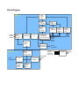
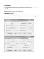
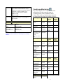
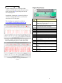
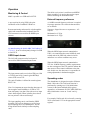
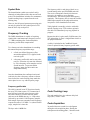
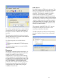
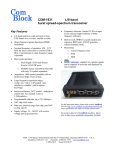
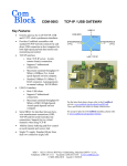
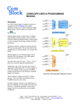
COM-1826 RECEIVER FOR TDRSS DEMAND ACCESS SERVICE o Key Features TDRSS DAS receiver including o SDDS-formatted input stream parsing o BPSK and SQPN spread-spectrum demodulation o Viterbi error correction 30-bin parallel code search for fast code acquisition. False code lock prevention. K=7 Rate ½ Viterbi decoding Built-in Bit Error Rate measurement for PRBS11 test sequences. Demodulation performances: within 1.5 dB from theory at threshold Eb/No of 2 dB. Demodulated bits encapsulated in UDP frames and sent out to the LAN. Support for IGMPv2 multicast addressing. Monitoring: ComScope –enabled: key internal signals can be captured in real-time and displayed on host computer. 90VAC – 264VAC power supply Programmable 2047-chip periodic I and Q Gold codes Programmable bit rates from 1 to 150 Kbits/s on each channel. Two independent bit synchronizers to acquire and track each channel bit stream. Receiver lock, Carrier frequency error, SNR For the latest data sheet, please refer to the ComBlock web site: http://www.comblock.com/download/com1826.pdf. These specifications are subject to change without notice. For an up-to-date list of ComBlock modules, please refer to http://www.comblock.com/product_list.html . MSS • 845-N Quince Orchard Boulevard • Gaithersburg, Maryland 20878 • U.S.A. Telephone: (240) 631-1111 Facsimile: (240) 631-1676 www.ComBlock.com © MSS 2014 Issued 8/6/2015 Block Diagram DSSS demodulator Code timing NCO Skip 1/2 chips State machine Code replica generation baseband complex samples Digital frequency translation Re-sampling LPF Carrier NCO PSK demodulator to PSK demodulator Despreading Coherent I&D Non-coherent I&D Despreading with on-time code replica Symbol timing NCO PSK symbol decoding Symbol timing loop Demodulated data bits False code lock detection Code tracking loop 3 x NACQ parallel detection circuits early center late bins to PSK demodulator Frequency error Code lock Carrier lock Noise power Carrier tracking loop (PLL+AFC) I&D Code acquisition Monitoring Monitoring Info Configuration This ComBlock assembly comprising several ComBlock modules can be monitored and controlled centrally over a single connection with a host computer. Connection types include built-in types: USB TCP-IP/LAN The module configuration is stored in non-volatile memory. Configuration (Basic) The easiest way to configure the COM-1826 is to use the ComBlock Control Center software supplied with the module on CD. In the ComBlock Control Center window detect the ComBlock module(s) by clicking the Detect button, next click to highlight the COM-1826 module to be configured, next click the Settings button to display the Settings window shown below. 3 Configuration (Advanced) Alternatively, users can access the full set of configuration features by specifying 8-bit control registers as listed below. These control registers can be set manually through the ComBlock Control Center or by software using the ComBlock API (see www.comblock.com/download/M&C_reference.pdf) All control registers are read/write. Definitions for the Control registers and Status registers are provided below. 4 Control Registers The module configuration parameters are stored in volatile (SRT command) or non-volatile memory (SRG command). All control registers are read/write. Several key parameters are computed on the basis of the 125 MHz internal processing clock fclk_p: frequency translation, chip rate, etc. Parameters SDDS-formatted stream input selection I Code Q Code Chip rate (fchip rate) Configuration 1 = UDP port 0x0500 = 1280 0 = TCP port 0x0400 = 1024 REG0(0) Linear feedback shift register initialization. As per [1] REG1 LSB REG2(2:0) MSb REG3 LSB REG4(2:0) MSb The nominal chip rate is 3.077799479166 Mchips/s. However, the design is somewhat more flexible. Alternative chip rates can be entered here 32-bit integer expressed as fchip rate * 232 / fclk_p. The maximum practical chip rate is fclk_p / 2. gain) Q channel spreading factor (Processing gain) Nominal input center frequency (fc) Reserved Spectrum inversion fsymbol_rate REG26(0) 0 = BPSK 1 = SQPN SQPN single/double source REG26(1) 0 = dual source: independent symbol rates on I and Q channels 1 = identical data on I and Q channels (prior to coherent sum) The maximum allowed error between transmitted and received chip rate is +/100ppm. Encoding REG5 (LSB) – REG8 (MSB) The I-channel symbol rate can be set independently of the spreading code period as fsymbol_rate * 232 / fclk_p AGC response time Example: “00346DC6” represents 100 Ksymbols/s. Q channel symbol rate fsymbol_rate I channel spreading factor (Processing REG9 (LSB) – REG12 (MSB) The Q-channel symbol rate can be set independently of the spreading code period as fsymbol_rate * 232 / fclk_p REG13 (LSB) – REG16 (MSB) Approximate (i.e rounded) ratio of chip rate / symbol rate REG17 (LSB) In addition to this fixed value, an optional time-dependent frequency profile can be entered. See frequency profile table. REG21 (LSB) – REG24 (MSB) REG25 Invert Q bit 0 = off 1 = on BPSK / SQPN Nominal chip rate: 0x064DA741 I channel symbol rate REG18(4:0) MSb Approximate (i.e rounded) ratio of chip rate / symbol rate REG19 (LSB) REG20(4:0) MSb The nominal center frequency is a fixed frequency offset applied to the SDDS input samples. It is used for fine frequency corrections, for example to correct clock drifts. 32-bit signed integer (2’s complement representation) expressed as fc * 232 / fclk_p REG26(2) 0 = NRZ-L 1 = NRZ-M 2 = NRZ-S 4 = Biphase-L REG26(5:3) Users can to optimize AGC response time while avoiding instabilities (depends on external factors such as gain signal filtering at the RF front-end and chip rate). The AGC_DAC gain control signal is updated as follows 0 = every chip, 1 = every 2 input chips, 2 = every 4 input chips, 3 = every 8 input chips, etc…. 10 = every 1000 input chips. Valid range 0 to 14. REG28(4:0) Viterbi decoding Disable (0) / Enable (1) REG27(1) Viterbi decoder G2 parity bit No (0) / Yes (1) REG27(2) 5 inversion Built-in test modulator (when instantiated) Parameters Configuration Digital Signal 16-bit amplitude scaling factor for the gain modulated signal. The maximum level should be adjusted to prevent saturation. The settings may vary slightly with the selected symbol rate. Therefore, we recommend checking for saturation when changing either the symbol rate or the signal gain. REG29 = LSB REG30 = MSB Additive White 16-bit amplitude scaling factor for Gaussian Noise additive white Gaussian noise. gain Because of the potential for saturation, please check for saturation when changing this parameter. REG31 = LSB REG32 = MSB Network Interface Parameters Configuration MAC addresses In order to ensure the uniqueness of LSB MAC addresses, users can define bits 7:1 through REG0(7:1). The MAC addresses upper bits (47:42) and (39:8) are automatically tied to the nearly unique FPGA DNA_ID. MAC address bit 0 is either 0 (LAN1) or 1 (LAN2). REG0(7:1). IP1 multicast 4-byte IPv4 address used for SDDS address input stream. (left LAN Example : 0x E1 00 00 01 designates connector on address 225.0.0.1 backpanel) Use 0.0.0.0 to signify that multicasting is not supported. REG33 (MSB) – REG36 (LSB) IP1 static address 4-byte IPv4 address used for SDDS (left LAN input stream. connector on Example : 0x AC 10 01 80 designates backpanel) address 172.16.1.128 The new address becomes effective immediately (no need to reset the ComBlock). REG37 (MSB) - REG40 (LSB) IP2 address (right 4-byte IPv4 address used for receiver LAN connector on output, monitoring and control. backpanel) Example : 0x AC 10 01 80 designates address 172.16.1.128 The new address becomes effective immediately (no need to reset the ComBlock). REG41 (MSB) - REG44 (LSB) Destination IP 4-byte IPv4 address address Destination IP address for UDP frames with decoded data. Example : 0x AC 10 01 80 designates address 172.16.1.128 The new address becomes effective immediately (no need to reset the ComBlock). REG45 (MSB) – REG48(LSB) Destination ports I-channel data is routed to this userdefined port number: REG49(LSB) – REG50(MSB) Q-channel data is routed to the incremented port number. Subnet mask REG51 (MSB) – REG54(LSB) Gateway IP address REG55 (MSB) – REG58(LSB) (Re-)Writing to the last control register REG58 is recommended after a configuration change to enact the change. 6 Status Registers Parameters Hardware selfcheck External 10 MHz presence Input sampling rate Time tag Input frame counter Missing input frame counter LAN1 MAC bad CRC counter MAC address Demodulator carrier lock status Code lock status Viterbi decoder1 synchronized Viterbi decoder2 synchronized Signal presence Decoder1 builtin BER Monitoring At power-up, the hardware platform performs a quick self check. The result is stored in status registers SREG0-9 Properly operating hardware will result in the following sequence being displayed: SREG0-SREG9 = 01 F1 1D xx 1F 93 10 22 22 03 1 = detected 0 = missing SREG9(0) The sampling rate, as read from the SDDS input stream. Format: sampling_rate/fclk *2^32 SREG10 = bit 7-0 (LSB) SREG11 = bit 15 – 8 SREG12 = bit 23 – 16 SREG13(3:0) = bit 27 – 24 (MSB) Last valid timetag read from the SDDS input header. Expressed in 250ps units. SREG14 (LSB) – SREG21(MSB) Cumulative SDDS frame counter. Each frame contains 1024 bytes = 256 complex samples. SREG22 (LSB) – SREG25(MSB) Cumulative number of missing SDDS frames. Should be zero. SREG26 (LSB) – SREG27(MSB) SREG28 (LSB) – SREG29(MSB) Unique 48-bit hardware address (802.3). In the form SREG30:SREG31:SREG32: …:SREG35 SREG36(0) 0 = unlocked or no input 1 = locked SREG36(1) 0 = unlocked or no input 1 = locked (1 s hysteresis) SREG36(2) 0 = not synchronized or no input 1 = synchronized SREG36(3) 0 = not synchronized or no input 1 = synchronized SREG36(4) 0 = no carrier detected in FFT 1 = carrier detected in FFT The Viterbi decoder computes the BER on the received (encoded) data stream Decoder2 builtin BER Nominal center frequency Carrier frequency offset1 Carrier frequency offset2 Despread signal power S Noise power N SNR irrespective of the transmitted bit stream. Encoded stream bit errors detected over a 1000-bit measurement window. SREG37 LSB SREG38 MSB The Viterbi decoder computes the BER on the received (encoded) data stream irrespective of the transmitted bit stream. Encoded stream bit errors detected over a 1000-bit measurement window. SREG39 LSB SREG40 MSB Expected center frequency: sum of the fixed center frequency and the dynamic frequency profile table. SREG41 (LSB) – SREG44 (MSB) Residual frequency offset with respect to the nominal carrier frequency (i.e. after frequency profile correction). Part 1/2. 32-bit signed integer expressed as fcerror * * 232 / fclk_p SREG45 (LSB) – SREG48 (MSB) Residual frequency offset with respect to the nominal carrier frequency (i.e. after frequency profile correction). Part 2/2. 32-bit signed integer expressed as fcerror * * 231 / fchip_rate SREG49 (LSB) – SREG52 (MSB) Average signal power after despreading. Compute the signal to noise ratio after despreading as S/N. The absolute value is meaningless because of multiple agcs. SREG53 (LSB) – SREG54 (MSB) Average noise power. Used to compute the SNR after despreading. The absolute value is meaningless because of multiple agcs. SREG55 (LSB) – SREG56 (MSB) 2*(S+N)/N ratio, valid only during code lock. Linear (not in dBs) Fixed point format 14.2 SREG57 (LSB) – SREG58 (MSB) 7 Bit error rate BER tester synchronized Monitors the BER (number of bit errors on the I-channel at the demodulator output, counted over 10,000 received bits) when the modulator is sending a PRBS-11 test sequence. Assume no FEC encoding. SREG59: LSB SREG60: MSB SREG36(5): 1 when the BER tester is synchronized with the received PRBS-11 test sequence. Built-in modulator SNR calibration Parameters Monitoring Measured SREG61(LSB) modulated signal SREG62 power SREG63(MSB) Measured AWGN SREG64(LSB) power (Noise SREG65 bandwidth is 6.25 SREG66(MSB) MHz) Multi-byte status variables are latched upon (re-)reading SREG7. ComScope Monitoring Key internal signals can be captured in real-time and displayed on a host computer using the ComScope feature of the ComBlock Control Center. Click on the button to start, then select the signal traces and trigger are defined as follows: Trace 1 signals Format Nominal sampling rate Input sampling rate 1 sample / symbol 1 sample/code epoch fclk Buffer length (samples) 512 1: Input signal Ichannel 8-bit signed 2: Demodulated Q-channel 8-bit signed 8-bit unsigned Nominal sampling rate Input sampling rate 2 samples/chip Buffer length (samples) 512 8-bit signed 8-bit signed 1 sample / symbol fclk 512 Trace 3 signals Format 1: Code tracking phase correction (accumulated) 2: Carrier fine tracking phase 3: I-Symbol tracking phase (accumulated) 4: Averaged noise power (valid only during code tracking) 8-bit signed Nominal sampling rate 2 samples / symbol Buffer length (samples) 512 8-bit signed 8-bit signed fclk 512 1 sample / symbol 512 8-bit signed fclk 512 Trigger Signal 1: Start of code replica Format Binary 3: Parallel correlator output 4: 2(S+N)/N after despreading. Valid only if code is locked. Linear (i.e. not in dBs) 8-bit unsigned Trace 2 signals Format 1: Input signal Qchannel 8-bit signed 2: Code replica. Compare with spread input signals 3: Demodulated Ichannel 8-bit signed 4: Averaged signal power (valid only during code tracking) 8 512 512 512 512 512 2. Code Lock Binary Signals sampling rates can be changed under software control by adjusting the decimation factor and/or selecting the fclk processing clock as realtime sampling clock. In particular, selecting the fclk processing clock as real-time sampling clock allows one to have the same time-scale for all signals. The ComScope user manual is available at www.comblock.com/download/comscope.pdf. Digital Test Points Test Point Definition A1 UDP/TCP input data activity. SDDS receive data valid flag from UDP or TCP. (8ns per input byte) SDDS input buffer underflow condition. ‘1’ when the sender is not fast enough. Recovered carrier/center frequency (coarse) Carrier lock Code lock Signal present Recovered chip clock Recovered I-channel symbol clock I-code start I-code replica I-channel before despreading (compare with code replica) Demodulated bit (I) Demodulated bit (Q) BER tester synchronized (I) when no FEC Byte error detected by BER tester (I) when no FEC Viterbi decoder (I) synchronized (pulse every 1K bits) Viterbi decoder (Q) synchronized (pulse every 1K bits) A2 A3 A4 A5 A6 A7 A8 A9 A10 A11 ComScope example, showing code lock with aligned: received spread signal (green) vs code replica (red) A12 A13 A14 A15 A16 A17 ComScope example: showing demodulated Ichannel 9 Operation Monitoring & Control M&C is possible over USB and LAN/TCP. The 64-bit receiver time is read from each SDDS frame preamble. It is used to time-tag the output frames containing the demodulated bits. External frequency reference A pre-requisite for using USB is the prior installation of the ComBlock USB driver. Remote monitoring and control is only through the right LAN connector on the backpanel (the left LAN connector is reserved for the SDDS input stream). At manufacturing, the default M&C LAN address is 172.16.1.1. It can be subsequently changed via USB or LAN/TCP. SDDS input stream The left LAN connector on the back panel is reserved for SDDS-formatted input stream. The input stream can be received on UDP port 1280 or TCP-IP port 1028. Control register REG0(0) selects UDP versus TCP. The static IP address is defined in control registers REG37-40. Note: It is important to ensure that the data source is fast enough to send 200 Mbits/s of UDP or TCP data with latency less than 2.5ms (the receiver input elastic buffer depth). When in doubt, please check the test point A2 with an oscilloscope. The input sampling rate is read from the SDDS preamble. The receiver design was verified at an input sampling rate of 6.25 MSamples/s, but the design should work similarly at other sampling rates. A 10 MHz external frequency reference is required for proper operation. The electrical characteristics are as follows: Sinewave, clipped sinewave or squarewave. ACcoupled. Minimum level: 2Vpp. Maximum level: 5Vpp. When the SDDS input stream is transmitted as UDP, it is essential that the same 10 MHz be used at both ends of the UDP link, otherwise buffer underflow or overflow conditions may occur. When the SDDS input stream is transmitted as TCP, the 10 MHz frequency stability requirements are not as stringent as the TCP protocol informs the data source of flow-control conditions at the data sink. In this case, the data source is responsible for timing adjustments in the data throughput. Spreading codes The demodulator is designed to acquire all Return Mode 2 link codes. The Gold code selection is performed by entering two 11-bit initialization vectors for the linear feedback shift registers. Appendix A of document 451-PN CODE-SNIP lists these initialization vectors as ‘I-code’ and ‘Qcode”. For example, NASA code 40 is selected by entering 2225o (octal) and 1337o in the appropriate control registers. 10 Symbol Rate The demodulation symbol rates on the I and Q channels are independent of the chip rate and code period. The demodulator includes two autonomous symbol tracking loops, separate from the code tracking loop. However, the full spread-spectrum processing gain can only be achieved if the symbol period is less than the 2047-chip code period. Frequency Tracking The DSSS demodulator is capable of acquiring signals with a maximum center frequency error of +/- 5 KHz remaining after fixed and dynamic (frequency profile table) compensation. The frequency table is read (played-back) every second starting at the specified SDDS start time. The receiver interpolates linearly 64x between successive 1s samples so as to minimize discontinuities. This ensures phase and frequency continuity. This frequency bias is removed from the SDDS input samples for the playback duration, irrespective of the demodulator lock status. Table playback is mutually exclusive with table upload. Opening a new TCP session to upload a new table will immediately stop any playback in progress. Because the table is quite small (131Kbits max), the TCP upload time (2-5ms) is insignificant relative to the playback duration. A utility is included in the ComBlock Control Center to upload a binary frequency profile table: Two features assist the demodulator in extending this natural frequency acquisition range: 1. a fixed user-defined frequency offset, entered through the GUI, is applied to the received signal. 2. a frequency profile table can be sent to the receiver. It consists of a start time followed by 32-bit frequency offset samples read at 1 second intervals. To prevent sudden frequency jumps, the table entries are interpolated linearly. Once the demodulator has confirmed carrier and code lock, the above frequency offsets are frozen. Once locked, the carrier tracking loops tracks the carrier phase over a very wide frequency range. Frequency profile table The table is entered in one TCP session whereby the user (TCP client) opens a TCP connection to port 1024 and writes the entire frequency table. The table consists of a 64-bit start time (same reference as the SDDS time tag, i.e. 250ps units) followed by up to 4096 32-bit frequency samples. Each sample represents a nominal center frequency expressed in units of 125 MHz / 232 (about 29 mHz steps), sampled at 1s intervals. The byte order is MSB first. Code Tracking Loop The code tracking loop is a coherent delay lock loop (DLL) of the 1st order. Code Acquisition 30 parallel detectors search for code aligment during the code acquisition phase. During the subsequent code tracking phase, 3 detectors track 11 the early/center/late code while the other 27 detectors scan for false lock. The detectors are staggered ½ chip apart. To manually update the software, highlight the ComBlock and click on the Swiss army knife button. Detection is performed in two steps: first a coherent detector averages the despread signal over ½ a symbol period. The result is squared and further averaged over 100 symbols. The received chip rate must be within +/- 4ppm of the nominal 3.077799479166 Mchips/s value. Demodulated data output The receiver can store multiple personalities. The list of personalities stored within the ComBlock Flash memory will be shown upon clicking on the Swiss army knife button. Demodulated data is encapsulated within variablelength UDP frames and send to the specified destination IP/Port. The output format is as follows: - fixed-length preamble consisting of (in the order of transmission) - 2-byte length of payload data (excluding preamble). In the range 1 to 1024 bytes. - 2-byte frame counter, modulo 216 - 4-byte currently undefined - 8-byte timestamp (last timestamp read from the SDDS input frames, latched at the first demodulated byte in the transmit frame). The output frames are sent when one of two trigger conditions is met: - at least 1024 demodulated data bytes are waiting in the transmit queue, or - at least 0.5second has elapsed since the last output frame and at least one demodulated data byte is waiting in the transmit queue. The default personality loaded at power up or after a reboot is identified by a ‘D’ in the Default column. Any unprotected personality can be updated while the Default personality is running. Select the personality index and click on the “Add/Modify” button. The payload data size is thus variable in the range 1 through 1024 bytes. Bytes are packed MSb first. Only full bytes are transmitted (no partially filled bytes). Load Software Updates From time to time, ComBlock software updates are released. 12 UDP Reset Port 1029 is open as a UDP receive-only port. This port serves a single purpose: being able to reset the modem (and therefore the TCP-IP connection) gracefully. This feature is intended to remedy a common practical problem: it is a common occurrence for one side of a TCP-IP connection to end abnormally without the other side knowing that the connection is broken (for example when a client ‘crashes’). In this case, new connections cannot be established without first closing the previous ones. The problem is particularly acute when the COM1826 is at a remote location. The software configuration files are named with the .bit extension. The bit file can be downloaded via the Internet, from the ComBlock CD or any other local file. The option and revision for the software currently running within the FPGA are listed at the bottom of the advanced settings window. The command “@001RST<CR><LF>” sent as a UDP packet to this port will reset all TCP-IP connections within the COM-1826. TCP-IP connections can also be cleared remotely from the ComBlock Control Center as illustrated below: Two firmware options are available for this receiver: -A firmware uses an internal VCTCXO frequency reference. -B firmware option requires an external 10 MHz frequency reference. Recovery This module is protected against corruption by an invalid FPGA configuration file (during firmware upgrade for example) or an invalid user configuration. To recover from such occurrence, connect a jumper in J3 and during power-up. This prevents the FPGA configuration and restore USB communication [LAN communication is restored only if the IP address is known/defined for the personality index selected as default]. Once this is done, the user can safely re-load a valid FPGA configuration file into flash memory using the ComBlock Control Center. 13 Troubleshooting Checklist Receiver does not communicate with the ComBlock Control Center: Make sure an external 10 MHz frequency reference is present prior to powering up the receiver. This applies only when the –B firmware option (external 10 MHz frequency reference) is selected by default. Demodulator can’t achieve lock even at high signalto-noise ratios: Make sure the modulator baseband I/Q signals do not saturate, as such saturation would strongly distort the modulation phase information. (this is a phase demodulator!) Demodulator can demodulate BPSK but not QPSK: A spectrum inversion may have occurred in the RF transmission chain. If so, invert the spectrum inversion flag at the demodulator. Configuration Management This specification is to be used in conjunction with VHDL software revision 0 and ComBlock control center revision 3.09a and above. It is possible to read back the option and version of the FPGA configuration currently active. Using the ComBlock Control Center, highlight the COM1826 module, then go to the advanced settings. The option and version are listed at the bottom of the configuration panel. Reference Documents [1] Space Network Interoperable PN Code Libraries 451-PN CODE-SNIP ComBlock Ordering Information COM-1826 Receiver for TDRSS DemandAccess Service MSS • 18221-A Flower Hill Way• Gaithersburg, Maryland 20879 • U.S.A. Telephone: (240) 631-1111 Facsimile: (240) 631-1676 E-mail: [email protected] 14