1
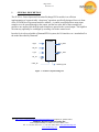
FC203A - Power Spectrum
Extraction/Exchange
FPGA Core
User’s Guide
Copyright © Sundance DSP Inc.
All rights reserved. No part of this document may be reproduced, translated,
stored in a retrieval system, or transmitted, in any form or by any means,
electronic, mechanical, photocopying, recording or otherwise, without prior
written permission of the owner.
Note:
If this copy is no longer in use, return to sender.
Page 2 of 2
Revision 0.5
AUTHORS
Name
F. Huettig
Signature
Date
8-Apr-07
DOCUMENT HISTORY
Date
19-Feb-07
2-Apr-07
3-Apr-07
5-Apr-07
8-Apr-07
Initials
FH
FH
FH
FH
FH
Revision
0.0
0.1
0.2
0.3
0.5
Description of Change
Initial Release for Internal Review
SPAN is now size of burst on each output stream
Input is always ready, output must be too
Fixed table 3
Added resource Info
Sundance Digital Signal Processing Inc.
4790 Caughlin Parkway 233, Reno, NV 89519-0907, U.S.A.
Tel: +1 (775) 827-3103, Fax: +1 (775) 827-3664, email: [email protected]
www.sundancedsp.com
Page 3 of 3
Revision 0.5
Table of Contents
1.
2.
3.
4.
5.
6.
7.
8.
GENERAL DESCRIPTION ................................................................................................... 4
I/O DESCRIPTION................................................................................................................. 5
PRESENTATION ................................................................................................................... 8
USAGE.................................................................................................................................... 8
VERIFICATION................................................................................................................... 10
DELIVERABLES ................................................................................................................. 11
LICENSING AND PROPERTY RIGHTS ........................................................................... 11
ORDERING INFORMATION ............................................................................................. 11
Table of Figures
Figure 1 – FC203A Component Diagram ....................................................................................... 4
Sundance Digital Signal Processing Inc.
4790 Caughlin Parkway 233, Reno, NV 89519-0907, U.S.A.
Tel: +1 (775) 827-3103, Fax: +1 (775) 827-3664, email: [email protected]
www.sundancedsp.com
Page 4 of 4
Revision 0.5
1.
GENERAL DESCRIPTION
The FC203A - Power Spectrum Extraction/Exchange FPGA module is an efficient
implementation of a general table “chop/swap” operation, specifically designed for use in front
of the FC203B Power Spectrum Interleave module. A control word defines how many input
samples are to be passed through to the output, and the low-order half of those samples are
passed to one output while the high-order samples are passed to the second output. The high/low
division may optionally be exchanged by asserting a bit in the control word.
In order for it to be used within a Diamond/FPGA system, the I/O interfaces are ‘standardized’ to
the model described by Diamond1.
FC203A
I0_IN
F0_OUT
Q0_IN
F1_OUT
I1_IN
64
Q1_IN
16
CTRL_IN
STATUS_OUT
Figure 1 – FC203A Component Diagram
1
See: http://www.3l.com/Diamond/Documentation/Diamond.pdf (Chapter 28, “FPGA Tasks”)
Sundance Digital Signal Processing Inc.
4790 Caughlin Parkway 233, Reno, NV 89519-0907, U.S.A.
Tel: +1 (775) 827-3103, Fax: +1 (775) 827-3664, email: [email protected]
www.sundancedsp.com
Page 5 of 5
Revision 0.5
2.
I/O DESCRIPTION
The FC203A component presents as a pure-FPGA ‘task’, and implements the following
interface:
Port Name
Channel Valid
Width
I0_IN,
0,
16
I1_IN
2
Q0_IN,
1,
16
Q1_IN
3
CTRL_IN
4
32
F0_OUT,
0,
64
F1_OUT
1
STATUS_OUT 2
32
Direction Description
Input
Input
Input
Output
Output
In-Phase Component, frequency-domain
data (2 channels)
Quadrature Component, frequency-domain
data (2 channels)
Control Word
In-phase/Quadrature components, 2channels each
Pass-through control/status
Table 1 –FC203A Interfaces
Additional port descriptions are provided below:
I0_IN .. I1_IN
There are two input ports for in-phase frequency domain streams. Data values are pairs of 16-bit
extended twos-complement as described in the FC108 User Manual, although the extended sign
value in bits 16-31 is ignored. These ports are suitable for connecting to the FC108-D’s I_OUT
ports.
Q0_IN .. Q1_IN
There are two input ports for the quadrature frequency streams. Data values are pairs of 16-bit
extended twos-complement as described in the FC108 User Manual. These ports are suitable for
connecting to the FC108-D’s Q_OUT ports.
NOTE: In agreement with the implementation of FC108, the input ports xn_IN are always
“ready” when any enable bit is set. To avoid the need for buffering in this module the
downstream data sinks must also be ready whenever this module has data to write. A FIFO may
be required at the output of this module to insure this.
NOTE: For simplicity, it is assumed that all four input channels (or the active subset) will
“write” at the same time. If this does not occur then the FC203A’s bin count will be in error on
some channels. There is currently no way to detect or report this condition.
CTRL_IN
Control miscellaneous parameters and features of the FC203A subcomponent. The port accepts
data one 32-bit word at a time.
Sundance Digital Signal Processing Inc.
4790 Caughlin Parkway 233, Reno, NV 89519-0907, U.S.A.
Tel: +1 (775) 827-3103, Fax: +1 (775) 827-3664, email: [email protected]
www.sundancedsp.com
Page 6 of 6
Revision 0.5
Signal
m
LOW_FREQ
SPAN
EXCHANGE
RESERVED
ENABLE
Bits
3..lsb
15..4
25..16
26
27
msb..28
Mode
R/W
R/W
R/W
R/W
R/W
R/W
Description
Configure m for input streams
Select lowest frequency bin
Select number of active frequency bins
Enable high/low exchange
Pass-through (reserved)
Output/function enable
Table 2 - FC203A Control Word
The FC203A sub-component ignores some of the bits in the control word; they exist to enable
the configuration of multiple modules (including FC203B) in a daisy-chain manner.
‘m’ determines the number of raw frequency component samples that are accepted at the Ix_IN
and Qx_IN ports to make up one frame. The relation between the frame size M and the control
word value ‘m’ is M=2m. After M samples are received on each input the internal count of bin
number is reset to zero. The maximum value of m is 12, corresponding to 4096 samples per
frame.
LOW_FREQ determines the frequency bin offset (from 0) which determines the start of the
spectral sampling on each of the input samples. All bins up to but not including LOW_FREQ are
discarded. If LOW_FREQ is zero, then no samples are discarded initially.
SPAN determines the number of frequency bins that will be passed along to each of the FC203A
outputs. Both F0_OUT and F1_OUT will receive SPAN samples on each frame. LOW_FREQ
+ 2 * SPAN must be less than M or the results will be undefined. SPAN is ten bits in size, a
value of zero indicates the maximum 1024 samples will be passed.
EXCHANGE determines if a spectral exchange of the low vs. high frequencies will be
performed on the streams. Low frequency bins are in the range [LOW_FREQ, LOW_FREQ +
SPAN – 1]. High frequency bins are in the range [LOW_FREQ + SPAN, LOW_FREQ + 2 *
SPAN – 1]. If EXCHANGE is zero, the low-frequency bins are passed to F0_OUT. If
EXCHANGE is one, the low-frequency bins are passed to F1_OUT.
ENABLE will cause the module to generate data on its output (F0_OUT, F1_OUT) ports if any
of the four bits are non-zero.
NOTE: To simplify the FPGA logic, the control word is assumed to be static while the module is
enabled. Changes to m, LOW_FREQ, SPAN, or EXCHANGE while any ENABLE bit is set may
result in unpredictable output.
F0_OUT, F1_OUT
These are dual-channel partitioned frequency data ports. Data values are groups of 64-bit values
in bursts of SPAN qwords. The 64-bit values consist of the in-phase and quadrature components
(16-bit two’s complement as described in the FC108 User Manual) of two channels. This port is
suitable for connecting to the Fx_IN ports of the FC203B subcomponent.
Bit 15..0
I0(0)
I0(1)
… I0(SPAN – 1)
Sundance Digital Signal Processing Inc.
4790 Caughlin Parkway 233, Reno, NV 89519-0907, U.S.A.
Tel: +1 (775) 827-3103, Fax: +1 (775) 827-3664, email: [email protected]
www.sundancedsp.com
Page 7 of 7
Revision 0.5
Bit 31..16 Q0(0) Q0(1) … Q0(SPAN – 1)
Bit 47..32 I1(0) I1(1) … I1(SPAN – 1)
Bit 63..48 Q1(0) Q1(1) … Q1(SPAN – 1)
Table 3 – Stream Format of Fx_OUT Port, low-frequency channel, LOW_FREQ = 0
STATUS_OUT
The module control/status word is driven on this channel; in this case all bits are passed
unchanged. This register may be read at any time, not just when a new control value has been
written. This port is suitable for connecting to a HOST port for the purpose of system state
feedback or to another FC203A or FC203B sub-component for daisy-chained configuration.
Sundance Digital Signal Processing Inc.
4790 Caughlin Parkway 233, Reno, NV 89519-0907, U.S.A.
Tel: +1 (775) 827-3103, Fax: +1 (775) 827-3664, email: [email protected]
www.sundancedsp.com
Page 8 of 8
Revision 0.5
3.
PRESENTATION
The firmware module is instantiated in a Diamond/FPGA configuration file as follows:
FC203A\
+---analysis\
+---fc203a\
+---specifications\
\---test\
Implementation Analysis
Task Source Code
Documentation
Verification Test Benches
Users of the FC203A firmware module will reference the Diamond .fcd file (top level) from the
fc203a\ above.
4.
USAGE
The firmware module is instantiated in a Diamond/FPGA configuration file as follows:
! declare tasks
!
task chop0
ins=5 outs=3
file="..\fc203a\fc203a.fcd"
!
! place tasks on FPGA
!
place chop0
<fpga>
!
! connect dataflow
!
connect ? <user_1>[w]
chop0[0]
connect ? <user_1>[x]
chop0[1]
connect ? <user_1>[y]
chop0[2]
connect ? <user_1>[z]
chop0[3]
connect ? <user_cfg>[n] chop0[4]
connect ? chop0[0]
<user_2>[a]
connect ? chop0[1]
<user_3>[b]
connect ? chop0[2]
<user_stat>[c]
Where <user_1> is a four-channel data source, <user_2> and <user_3> are data-sink
tasks, and <user_stat> is a status-sink task. <user_cfg> is a connection which supplies
the 32-bit configuration control word.
Sundance Digital Signal Processing Inc.
4790 Caughlin Parkway 233, Reno, NV 89519-0907, U.S.A.
Tel: +1 (775) 827-3103, Fax: +1 (775) 827-3664, email: [email protected]
www.sundancedsp.com
Page 9 of 9
Revision 0.5
In some cases, it is useful to provide some amount of elastic buffering before or after the
FC203A task in order to help close timing in the FPGA design. This can be accomplished as
follows:
! declare tasks
!
task fifo1
ins=1 outs=1
task chop0
ins=5 outs=3
task fifo2
ins=1 outs=1
!
! place tasks on FPGA
!
place fifo1
<fpga>
place chop0
<fpga>
place fifo2
<fpga>
!
! connect dataflow
!
connect C1
<user_1>[x]
connect ?
fifo1[0]
! …repeat for other inputs…
connect C2
<user_cfg>[y]
connect ?
chop0[0]
connect C3
fifo2[0]
! …repeat for other outputs…
file="..\fifo\fifo8.fcd"
file="..\fc203a\fc203a.fcd"
file="..\fifo\fifo8.fcd"
fifo1[0]
chop0[0]
chop0[4]
fifo2[0]
<user_2>[z]
Note: When implementing on some FPGA devices, a slower clock may be needed.
In order to close timing on some (slow) FPGA device/speed grades, the task may need to run
under a slower clock. To do this, use Diamond's facility to generate a custom clock, and provide
this clock to each FC203A instance.
See the 3L/Diamond User Guide v3.1.3 pg. 306 for additional details.
For example:
! Use a slower clock for the UUT
!
clock slow processor=<fpga> source=DEFAULT output=50MHz
!
! place tasks on FPGA
!
place chop0
<fpga>
clock=slow
Sundance Digital Signal Processing Inc.
4790 Caughlin Parkway 233, Reno, NV 89519-0907, U.S.A.
Tel: +1 (775) 827-3103, Fax: +1 (775) 827-3664, email: [email protected]
www.sundancedsp.com
Page 10 of 10
Revision 0.5
5.
VERIFICATION
The firmware module will be supported by two types of test benches. In all cases, compilation is
performed using gmake (distributed with CCS3.0 or greater)2.
Unit Test Benches
A C- Reference Model is implemented as a Diamond/DSP Task. This model is not yet
implemented as of this revision.
Resource and Performance Analysis Benches
A mechanism to obtain the resource utilization of the FC203A core is provided. The basic
principle is to generate a “baseline” implementation of the target FPGA that contains a ‘stub’.
The ‘stub’ has all the same inputs and outputs, but is a trivial implementation of the FPGA task.
This “baseline” is compared to a real instantiation of the FC203A module. The stub FPGA task
is provided as ‘FC203A\FC203A_base.fcd’.
Comparing the two MAP report files and subtracting the Slices, BRAM and MPY in use
provides an accurate real-word estimate of the resources used by the FC203A module.
Finally, Diamond application configuration files are provided which enable the FC203A module
to be instantiated into a supported single (stand-alone) FPGA board. By connecting the dataflow
inputs of the FC203A to SDB resources, and the CTRL_IN to the default Comport (CP3,
typically) resource, a hardware reference is created which can be added to any system and
operated at line rate.
The configuration files and makefile for accomplishing these are provided in the analysis\
folder.
MODULE
SMT348-10
SMT365-8-1
SMT368-10
SMT368-12
SMT398-8000
SMT398-VP70
SMT417
FPGA
XC4VSX55-10
XC2V1000-4
XC4VSX35-10
XC4VSX35-12
XC2V8000-4
XC2VP70-6
XC2VP50-5
Slices
110
108
110
110
108
100
99
BRAM
0
0
0
0
0
0
0
MPY
0
0
0
0
0
0
0
FMAX (MHz)
262
172
262
331
172
227
202
Notes
Table 4 –FC203A Performance Estimates and Resource Utilization
The results in table 4 are estimates only, based on very lightly-loaded FPGA configurations.
Some trade-off between slice usage and speed is possible depending on synthesis and fitting
options. Exceeding FMAX may cause logic errors and unexpected results, which can be
exceedingly hard to debug. It is the system designer’s responsibility to avoid this condition.
2
Only gmake has the necessary syntax to effectively implement the build system. Contact Sundance DSP for
assistance if your installation lacks CCS.
Sundance Digital Signal Processing Inc.
4790 Caughlin Parkway 233, Reno, NV 89519-0907, U.S.A.
Tel: +1 (775) 827-3103, Fax: +1 (775) 827-3664, email: [email protected]
www.sundancedsp.com
Page 11 of 11
Revision 0.5
6.
DELIVERABLES
FC203A is a complete Diamond/FPGA firmware module that includes:
•
•
•
•
•
•
7.
Firmware source (.vhd) files
Diamond/FPGA integration support (.fcd, _pkg.vhd) and example implementations
VHDL Module-level testbench (included with FC203B)
C Simulation harness [NOTE: Not available in Release 0.1]
Matlab analysis tools [NOTE: Not available in Release 0.1]
User Guide
LICENSING AND PROPERTY RIGHTS
Sundance DSP retains copyright and licensing rights, and distributes the FC203A firmware
module under non-disclosure agreement only. Special arrangements are made on a case-by-case
basis.
All customers need to purchase support contracts from Sundance DSP in order to be able to
obtain updates and technical support for the FC203A firmware module.
For support, please register on http://support.sundancedsp.com and post all questions on the
forum. You can also contact any of Sundance offices, around the world, by telephone or email.
For details, please see the Sundance web site at http://www.sundancedsp.com
8.
ORDERING INFORMATION
The FC203A component may be ordered separately, or bundled with any other package
containing multiple products. Contact Sundance DSP for specific details.
Sundance Digital Signal Processing Inc.
4790 Caughlin Parkway 233, Reno, NV 89519-0907, U.S.A.
Tel: +1 (775) 827-3103, Fax: +1 (775) 827-3664, email: [email protected]
www.sundancedsp.com