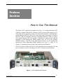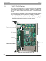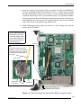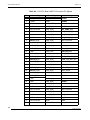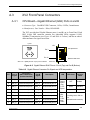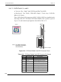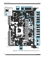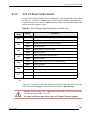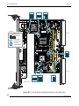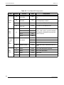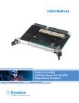
1
User Manual XV2 Intel® Quad-Core Xeon® CPU / 1.73 GHz / 6RU VME64 Platform XV2 Intel® Quad-Core Xeon® CPU, VME64 Platform XV2 Intel® Quad-Core Xeon® CPU, VME64 Platform XV2 Intel® Quad-Core Xeon® CPU, VME64 Platform XV2 Intel® Quad-Core Xeon® CPU, VME64 Platform XV2 Intel® Quad-Core Xeon® CPU, VME64 Platform XV2 Intel® Quad-Core Xeon® CPU, VME64 Platform XV2 Intel® Quad-Core Xeon® CPU, VME64 Platform XV2 Hardware Manual Version 1.0—August 2011 Themis Computer—Americas and Pacific Rim 47200 Bayside Parkway Fremont, CA 94538 Phone (510) 252-0870 Fax (510) 490-5529 World Wide Web http://www.themis.com Themis Computer—Rest of World 5 Rue Irene Joliot-Curie 38320 Eybens, France Phone +33 476 14 77 80 Fax +33 476 14 77 89 Copyright © 2011 Themis Computer, Inc. ALL RIGHTS RESERVED. No part of this publication may be reproduced in any form, by photocopy, microfilm, retrieval system, or by any other means now known or hereafter invented without the prior written permission of Themis Computer. The information in this publication has been carefully checked and is believed to be accurate. However, Themis Computer assumes no responsibility for inaccuracies. Themis Computer retains the right to make changes to this publication at any time without prior notice. Themis Computer does not assume any liability arising from the application or use of this publication or the product(s) described herein. RESTRICTED RIGHTS LEGEND: Use, duplication, or disclosure by the United States Government is subject to the restrictions set forth in DFARS 252.227-7013 (c)(1)(ii) and FAR 52.227-19. TRADEMARKS Themis® is a registered trademark of Themis Computer, Inc. XV2™ is a trademark of Themis Computer, Inc. Intel® and Xeon® are registered trademarks of Intel Corporation. Core™ is a trademark of Intel Corporation. Tsi148™ is a trademark of the Tundra Semiconductor Corporation. All other trademarks or registered trademarks used in this publication are the property of their respective owners. CE Marking This product complies with the European EMC Directive (2004/108/EC) and the European Low Voltage Safety Directive (2006/95/EC)/. Safety Precautions Instructions regarding safety precautions during installation, operation, or maintenance of the equipment are given in the section entitled “Safety Instructions” on page iv. WARNINGS and CAUTIONS The definitions of WARNINGS and CAUTIONS as used in this document are given in the Preface in the section entitled “Notes, Cautions, Warnings, and Sidebars” on page xviii. Themis Customer Support North America, South America, and Pacific Rim Telephone: Fax: E-mail: Web Site: XV2 Hardware Manual, Version 1.0 August 2011 Part Number: 118156-022 510-252-0870 510-490-5529 [email protected] http://www.themis.com Version Revision History Version 1.0.........................................................................................August 2011 Themis Computer iii XV2 Hardware Manual Version 1.0 Safety Instructions To maximize user safety and ensure correct device operation, all instructions contained in this section should be read carefully. Caution: It is important that the user observe all warnings and instructions that are on the device and contained in this manual. • The device must be used in accordance with the instructions for use. • Electrical installations in the room must correspond to the requirements of respective regulations. • Take care that there are no cables, particularly mains cables, in areas where persons can trip over them. • Do not use a mains connection in sockets shared by a number of other power consumers. Do not use an extension cable. • Do not set up the device in the proximity of heat sources or in a damp location. Make sure the device has adequate ventilation. • All connection cables must be screwed or locked to the chassis housing. • The device is no longer safe to operate when — the device has visible damage or — the device no longer functions. • In these cases, the device must be shut down and secured against unintentional operation. • Repairs may only be carried out by a person authorized by Themis Computer. • If extensions are made to the device, the legal stipulations and the device specifications must be observed. Electrostatic Discharge (ESD) A sudden discharge of electrostatic electricity can destroy static-sensitive devices or micro-circuitry. Proper packaging and grounding techniques are necessary precautions to prevent damage. Always take the following precautions: iv Themis Computer Safety Instructions 1. Transport boards in static-safe containers such as boxes or bags. 2. Keep electrostatic-sensitive parts in their containers until they arrive at staticfree stations. 3. Always be properly grounded when touching a sensitive board, component, or assembly. 4. Store electrostatic-sensitive boards in protective packaging or on conductive foam. Grounding Methods Guard against electrostatic damage at workstations by following these steps: 1. Cover workstations with approved anti-static material. Provide a wrist strap connected to a work surface and properly grounded tools and equipment. 2. Use anti-static mats, heel straps, or air ionizers to give added protection. 3. Handle electrostatic-sensitive components, boards, and assemblies by the case or the PCB edge. 4. Avoid contact with pins, leads, or circuitry. 5. Turn off power and input signals before inserting and removing connectors or test equipment. 6. Keep the work area free of non-conductive materials such as ordinary plastic assembly aids and Styrofoam. 7. Use field service tools, such as cutters and screwdrivers, that are conductive. 8. Always place drives and boards PCB-assembly-side down on the foam. Instructions for the Lithium Battery Motherboards are installed with a lithium battery. To replace this battery, please observe the instructions that are described in this manual. Warning: There is a danger of explosion when the wrong type of battery is used as a replacement. Themis Computer v XV2 Hardware Manual vi Version 1.0 Themis Computer Table of Contents Version Revision History ...................................................................................................... iii Safety Instructions ................................................................................................................ iv Chapter Overview .............................................................................................................. xvii 1. XV2 Installation ............................................................................................................ 1-1 1.1 Determine Board Type ........................................................................................... 1-1 1.2 Check Configurations ............................................................................................ 1-2 1.3 Install the Paddle Cards ......................................................................................... 1-3 1.3.1 CPU Board Paddle Card (Optional) ........................................................... 1-3 1.3.2 I/O Board Paddle Card (Optional if No XMC Module) ............................ 1-4 1.4 Attach Front-Panel I/O Cables ............................................................................... 1-7 1.4.1 CPU Board ................................................................................................. 1-7 1.4.1.1 Gigabit Ethernet Ports A and B .................................................. 1-7 1.4.1.2 BMC Connector .......................................................................... 1-8 1.4.1.3 USB Ports A, B, C, and D ........................................................... 1-8 1.4.1.4 Serial Port COM1 ....................................................................... 1-8 1.4.1.5 SATA Ports A and B .................................................................. 1-8 1.4.1.6 High-Definition (HD) Audio Ports ............................................. 1-8 1.4.2 I/O Board ................................................................................................... 1-8 1.4.2.1 4-Channel SAS/SATA Port ........................................................ 1-8 1.4.2.2 VGA Graphics Port ..................................................................... 1-9 1.4.2.3 XMC/PMC Module Ports ........................................................... 1-9 1.5 Attach Paddle-Card Cables .................................................................................... 1-9 1.5.1 CPU Board Paddle Card ............................................................................ 1-9 1.5.1.1 SATA Ports 2, 3, and 4 ............................................................... 1-9 1.5.1.2 High-Definition (HD) Audio Ports ............................................. 1-9 1.5.1.3 PS/2 Keyboard & Mouse .......................................................... 1-10 1.5.1.4 USB Ports 3, 4, 6, and 7 ............................................................ 1-10 1.5.1.5 Serial Ports COM1 and COM2 ................................................. 1-10 1.5.2 I/O Board Paddle Card ............................................................................. 1-10 Themis Computer vii XV2 Hardware Manual Version 1.0 1.5.2.1 SAS/SATA Port ........................................................................ 1-10 1.5.2.2 VGA Graphics Port ................................................................... 1-10 1.5.2.3 Gigabit Ethernet Ports A and B (LANA, LANB) ..................... 1-10 1.5.3 Auxiliary +12V/+5V Power Connectors ................................................. 1-11 1.6 Daisy-Chain Jumper Settings ............................................................................... 1-11 1.7 TOD/NVRAM Battery ........................................................................................ 1-12 1.8 Program the XV2 Power-Up Delay Using the BMC Serial Port ........................ 1-14 2. XV2 Features and Specifications ................................................................................. 2-1 2.1 Basic Features ........................................................................................................ 2-1 2.2 XMC/PMC Modules .............................................................................................. 2-5 2.3 Paddle Cards .......................................................................................................... 2-5 2.4 XMC/PMC Carrier Boards .................................................................................... 2-6 2.5 System Specifications ............................................................................................ 2-6 2.5.1 Processor and Memory Subsystems .......................................................... 2-6 2.5.2 Operating Systems ..................................................................................... 2-7 2.5.3 Auxiliary Functions ................................................................................... 2-7 2.6 Environmental Specifications ................................................................................ 2-8 2.7 Regulatory Compliance ......................................................................................... 2-9 2.8 Nominal Power Requirements ............................................................................... 2-9 3. Hardware Overview ...................................................................................................... 3-1 3.1 CPU Board ............................................................................................................. 3-1 3.1.1 Intel LC5518 Quad-Core Xeon Processor ................................................. 3-1 3.1.2 Intel 3420 Platform Controller Hub (PCH) ............................................... 3-1 3.1.3 82571EB Dual Gigabit Ethernet Controller ............................................... 3-2 3.1.4 WPCD374L Super I/O (SIO) Controller ................................................... 3-3 3.1.5 Tundra Tsi148 PCI/X-to-VME Bridge ...................................................... 3-3 3.1.6 Realtek ALC262 High-Definition Audio Codec ....................................... 3-4 3.1.7 Programmable Logic .................................................................................. 3-5 3.2 XMC/PMC Carrier Boards ..................................................................................... 3-5 Appendix A. Connector Pinouts and Signal Descriptions ............................................ A-1 A.1 CPU Board—XV2 Rear Connectors .................................................................... A-1 viii Themis Computer Table of Contents A.1.1 VME P1 Connector (CPU Board) ............................................................ A-1 A.1.2 VME P2 Connector (CPU Board) ............................................................ A-3 A.2 I/O Board—XV2 Rear Connectors ....................................................................... A-5 A.2.1 VME P1 Connector (I/O Board) ............................................................... A-5 A.2.2 VME P2 Connector (I/O Board) ............................................................... A-7 A.3 XV2 Front-Panel Connectors ................................................................................ A-9 A.3.1 CPU Board—Gigabit Ethernet (GbE) Ports A and B ............................... A-9 A.3.2 CPU Board—BMC Port ......................................................................... A-10 A.3.3 CPU Board—USB Ports A, B, C, and D ................................................ A-11 A.3.4 CPU Board—Serial Port COM1 ............................................................. A-12 A.3.5 CPU Board—SATA Ports A and B ........................................................ A-13 A.3.6 CPU Board—Stereo Audio In and Audio Out Jacks .............................. A-14 A.3.7 I/O Board—Multiple SAS/SATA Ports ................................................. A-14 A.3.8 I/O Board—VGA Graphics Port ............................................................. A-16 A.4 Push-Button RESET ........................................................................................... A-17 A.5 XV2 XMC/PMC Module Card Connectors ........................................................ A-17 A.5.1 PMC Connectors ..................................................................................... A-17 A.5.2 XMC Connectors .................................................................................... A-24 A.6 XV2 P2 Paddle Cards ......................................................................................... A-28 A.6.1 CPU Board Paddle Card ......................................................................... A-28 A.6.1.1 DIN-8 PS/2 Keyboard/Mouse Connector ................................ A-28 A.6.1.2 USB Ports USB3 / USB4 and USB6 / USB7 .......................... A-29 A.6.1.3 SATA Ports 3, 4, and 5 ............................................................ A-30 A.6.2 I/O Board Paddle Card ............................................................................ A-31 A.6.2.1 VGA Monitor Port ................................................................... A-31 A.6.2.2 Gigabit Ethernet (GbE) Ports C and D .................................... A-32 A.6.2.3 SAS/SATA Port ....................................................................... A-33 A.6.2.4 Auxiliary +12-Volt/+5-Volt Power Connectors ...................... A-34 Appendix B. Jumper Pins and Solder Beads ..................................................................B-1 B.1 Field-Configurable Jumper Pins ............................................................................B-1 B.1.1 XV2 CPU Board Jumper Pins ...................................................................B-1 B.1.2 XV2 I/O Board Jumper Pins ......................................................................B-1 B.1.3 Memory Module Jumper Pins ....................................................................B-2 B.2 Factory-Configurable Solder Beads .......................................................................B-2 Themis Computer ix XV2 Hardware Manual Version 1.0 B.2.1 XV2 CPU Board Solder Beads ..................................................................B-2 B.2.2 XV2 I/O Board Solder Beads ....................................................................B-5 B.2.3 Memory Module Solder Beads ..................................................................B-7 Appendix C. Front-Panel I/O Connections and LEDs ...................................................C-1 C.1 Introduction ............................................................................................................C-1 C.1.1 Front-Panel Dimensions ............................................................................C-1 C.1.2 Injector/Ejector Handles ............................................................................C-2 C.1.2.1 VME64-type Handles .................................................................C-2 C.1.2.2 Legacy-VME Handles ................................................................C-2 C.2 XV2 Front Panels ...................................................................................................C-3 C.2.1 XV2/1 Front Panel .....................................................................................C-4 C.3 XV2 Front-Panel LEDs .........................................................................................C-5 Appendix D. Board Component and Connector Diagrams .......................................... D-1 D.1 XV2 CPU Board ................................................................................................... D-1 D.2 XV2 I/O Board ...................................................................................................... D-1 D.3 Memory Module ................................................................................................... D-4 Appendix E. VME Slot Configurations ...........................................................................E-1 Appendix F. Re-Packing Instructions ............................................................................. F-1 F.1 Re-Packaging for Shipment ................................................................................... F-1 F.2 Packing Components ............................................................................................. F-2 F.3 Instructions for Re-Packing ................................................................................... F-3 Index............................................................................................................................... Index-1 Reader Comment Card x Themis Computer Table of Contents List of Figures Figure 1 XV2 Single-Board Computer ............................................................................ xv Figure 1-1 CPU Board Paddle Card Connector Diagram (Top Side) ............................... 1-5 Figure 1-2 I/O Board Paddle Card Connector Diagram (Top Side).................................. 1-6 Figure 1-3 Remove SDRAM 1 from its Slot ................................................................... 1-12 Figure 1-4 Insert the Orange Stick and Push the Battery through its Holder .................. 1-13 Figure 2-1 XV2 CPU Board and I/O Board Block Diagram............................................. 2-3 Figure A-1 XV2 CPU Board VME P1 Connector Pinout ................................................. A-1 Figure A-2 XV2 CPU Board VME P2 Connector Pinout ................................................. A-3 Figure A-3 XV2 I/O Board VME P1 Connector Pinout ................................................... A-5 Figure A-4 XV2 I/O Board VME P2 Connector Pinout ................................................... A-7 Figure A-5 Gigabit Ethernet RJ45 Pinout—Port A (Top) and Port B (Bottom)............... A-9 Figure A-6 XV2 BMC Connector Pinout........................................................................ A-10 Figure A-7 XV2 Dual USB Connector Pinout ................................................................ A-11 Figure A-8 XV2 Serial Port COM1 RJ45 Connector Pinout .......................................... A-12 Figure A-9 XV2 Dual SATA Connector Pinout ............................................................. A-13 Figure A-10 XV2 SAS/SATA Connector Pinout.............................................................. A-14 Figure A-11 XV2 VGA Graphics Connector Pinout ....................................................... A-16 Figure A-12 XV2 PMC Module Card Connector (3 required per Module)...................... A-17 Figure A-13 XV2 XMC Module Card Connector (1 required per Module) ..................... A-24 Figure A-14 CPU Board Paddle Card PS/2 Mini-DIN Connector Pinout ........................ A-28 Figure A-15 CPU Board Paddle Card Dual USB Ports 3/4 and 6/7 Connector Pinout .... A-29 Figure A-16 CPU Board Paddle Card SATA Connector Pinout....................................... A-30 Figure A-17 I/O Board P2 Paddle Card VGA Connector Pinout...................................... A-31 Figure A-18 Gigabit Ethernet RJ45 Pinout—Port C (Bottom) and Port D (Top)............. A-32 Figure A-19 I/O Board SATA Connector Pinout.............................................................. A-33 Figure A-20 P2 Paddle Card Power Connector Pinouts.................................................... A-34 Themis Computer xi XV2 Hardware Manual Version 1.0 Figure B-1 XV2 CPU Board Solder-Bead Locations (Bottom Side Only)........................ B-4 Figure B-2 XV2 I/O Board Solder-Bead Locations (Top Side Only)................................ B-6 Figure C-1 XMC/PMC Injector/Ejector Handles............................................................... C-3 Figure C-2 XV2/1 Front Panel ........................................................................................... C-4 Figure C-3 XV2 Front-Panel LEDs ................................................................................... C-5 Figure D-1 XV2 CPU Board Component and Connector Diagram (Top Side)................ D-2 Figure D-2 XV2 I/O Board Component and Connector Diagram (Top Side) .................. D-3 Figure E-1 XV2 VME Slot Configurations ....................................................................... E-2 Figure F-1 Packaging Components.................................................................................... F-2 Figure F-2 Order of Assembly........................................................................................... F-4 xii Themis Computer Table of Contents List of Tables Table 1-1 XV2 CPU Board P2 Paddle Card I/O Connections ......................................... 1-3 Table 1-2 XV2 I/O Board P2 Paddle Card I/O Connections ........................................... 1-4 Table 1-3 XV2 Integration Kit (Order-Dependent) ......................................................... 1-6 Table 1-4 XV2 Front-Panel I/O Connections .................................................................. 1-7 Table 2-1 XV2 Front-Panel I/O Connections .................................................................. 2-2 Table 2-2 Processor Specifications .................................................................................. 2-6 Table 2-3 Memory Specifications .................................................................................... 2-6 Table 2-4 Auxiliary Functions Specifications.................................................................. 2-7 Table 2-5 XV2 Environmental Specifications ................................................................. 2-8 Table 2-6 XV2 Regulatory Compliance........................................................................... 2-9 Table 2-7 Nominal XV2 Power Requirements, 12-GB Memory Modules...................... 2-9 Table A-1 XV2 CPU Board VME P1 Connector-Pin Signals ......................................... A-2 Table A-2 XV2 CPU Board VME P2 Connector-Pin Signals ......................................... A-4 Table A-3 XV2 I/O Board VME P1 Connector-Pin Signals ........................................... A-5 Table A-4 I/O Board XV2 VME P2 Connector-Pin Signals ........................................... A-8 Table A-5 Gigabit Ethernet Connector-Pin Signals and LED Interpretation .................. A-9 Table A-6 XV2 BMC Connector-Pin Signals................................................................ A-10 Table A-7 XV2 Dual USB Connector-Pin Signals ........................................................ A-11 Table A-8 XV2 Serial Port COM1 RJ45 Connector-Pin Signals .................................. A-12 Table A-9 XV2 Dual SATA Connector-Pin Signals ..................................................... A-13 Table A-10 XV2 Stereo Audio Connector-Pin Signals ................................................... A-14 Table A-11 XV2 SAS/SATA Connector-Pin Signals...................................................... A-15 Table A-12 XV2 VGA Graphics Connector-Pin Signals ............................................... A-16 Table A-13 XV2 PMC Module Card Connector J4 Signals (32 bit) ............................... A-18 Table A-14 XV2 PMC Module Card Connector J5 Signals (32 bit) ............................... A-19 Themis Computer xiii XV2 Hardware Manual Version 1.0 Table A-15 XV2 PMC Module Card Connector J6 Signals (64 bit) ............................... A-20 Table A-16 XV2 PMC Module Card Connector J7 Signals (32 bit) ............................... A-21 Table A-17 XV2 PMC Module Card Connector J8 Signals (32 bit) ............................... A-22 Table A-18 XV2 PMC Module Card Connectors J9 Signals (64 bit).............................. A-23 Table A-19 XV2 XMC Module Card Connector J10 Signals ......................................... A-24 Table A-20 XV2 XMC Module Card Connector J11 Signals ......................................... A-26 Table A-21 CPU Board Paddle Card PS/2 Connector-Pin Signals.................................. A-28 Table A-22 USB Ports 3/4 and 6/7 Connector-Pin Signals ............................................ A-29 Table A-23 CPU Board Paddle Card SATA Connector-Pin Signals.............................. A-30 Table A-24 I/O Board P2 Paddle Card VGA Connector-Pin Signals............................. A-31 Table A-25 Gigabit Ethernet Connector-Pin Signals and LED Interpretation ................ A-32 Table A-26 I/O Board SAS/SATA Connector-Pin Signals ............................................ A-33 Table A-27 +12V/+5V Power Connector-Pin Signals..................................................... A-34 Table B-1 XV2 CPU Board Solder-Bead Settings (Bottom Side Only) .......................... B-2 Table B-2 XV2 I/O Board Solder-Bead Settings (Top Side Only) .................................. B-5 Table C-1 XV2 Model Configurations ............................................................................. C-1 Table C-2 Front-Panel LED Interpretation ....................................................................... C-6 Table E-1 XV2 Model Configurations ............................................................................. E-1 xiv Themis Computer Preface Section How to Use This Manual The Themis XV2 single-board computer (see Figure 1) is a high-performance 6RU VME-bus computer with an Intel® quad-core Xeon™ processor that operates at 1.73 GHz clock speed. It supports a variety of I/O from the Front Panel—including BMC, gigabit Ethernet, USB 2.0, SATA, SAS, serial, audio, and VGA graphics—as well as from the VME P2 backplane connector—including KB/mouse, USB 2.0, SATA, SAS, gigabit Ethernet, and VGA graphics. Connection to signals on the VME P2 backplane is made through two Themis Paddle Cards. Up to 24 GB of DDR3 SDRAM memory—with ECC Error Detection/Correction—can be installed and operated over three independent DDR3 channels (see Figure 2-1, page 2-3, in Chapter 2). Operating systems include Linux and Microsoft Windows. This XV2 Hardware Manual [P/N 118156-022] describes how to install the XV2 and gives a hardware overview, including a list of XV2 features and specifications. Figure 1. XV2 Single-Board Computer Themis Computer xv XV2 Hardware Manual Version 1.0 XV2 users may obtain greater graphics capability than the onboard XV2 graphics by installing a T2GPX XMC Graphics Card in a XV2 XMC/PMC module slot. Themis Computer values its customer comments and opinions; therefore, a “Reader Comment Card” is located at the end of this manual for your use. Please take the time to fill out this card with any comments concerning Themis products and services, and return it to Themis Computer. Your comments may also be forwarded to Themis by sending email to [email protected]. Before you begin, carefully read each of the procedures in this manual. Serious damage can be caused by improper handling of the equipment. Intended Audience This manual is written for system integrators and programmers. It contains all necessary information for installation and configuration of the XV2 and assumes the UEFI program code is installed in the system Flash memory. If you intend to operate the XV2 with an operating system other than Linux or Windows, please consult the appropriate documentation supplements accompanying your OS or kernel software. Programmers wishing to write code for the XV2 without the benefit of an operating system or real-time kernel will require additional data sheets. The reader should have a working knowledge of VMEbus and PCI local bus standards, as well as Ethernet and SATA specifications. Unpacking Caution: The XV2 contains statically sensitive components. Industry-standard antistatic measures must be observed when removing the XV2 from its shipping container and during any subsequent handling. A wrist strap provides grounding for static electricity between your body and the chassis of the system unit. Remove the XV2 and accessories from the shipping container and check the contents against the packing list. Be certain to observe industry-standard ESD protection procedures when handling static-sensitive components. The package should include all elements of your order. Please report any shipping discrepancies to the Themis Computer Customer Support group immediately: [email protected] or 1-510-252-0870. xvi Themis Computer How to Use This Manual When sending the XV2 back to Themis for any reason, the customer must use the original shipping container, packed exactly as described in Appendix F, “Re-Packing Instructions”, of this manual. To ship the XV2 without following the procedures outlined in Appendix F may invalidate the warrantee. Chapter Overview The chapters and appendices of this manual are briefly outlined as follows: • Chapter 1, "XV2 Installation", provides instructions on the installation and configuration of the XV2 for your particular environment and application. Note: The information contained in Chapter 1 is mandatory to understand and configure the correct operation of the XV2. This chapter should be read in its entirety. • Chapter 2, "XV2 Features and Specifications", provides a brief overview of the XV2, along with its System, Environmental, and Power specifications. • Chapter 3, "Hardware Overview", describes the major components installed on the XV2. • Appendix A, “Connector Pinouts and Signal Descriptions”, provides part numbers, pinouts, and signal descriptions for the I/O connectors on the XV2 Baseboard and Paddle Card. • Appendix B, "Jumper Pins and Solder Beads", provides a detailed description and default configuration of each of the jumper pins and solder beads on the XV2, as well as diagrams illustrating their location on the PCB. Note: Appendix B should be consulted to verify that the jumper pins and solder beads on your system are set to meet your application requirements. • Appendix C, “Front-Panel I/O Connections and LEDs”, illustrates the Front Panels for all model configurations of the XV2. • Appendix D, “Board Component and Connector Diagrams”, provides descriptions of the major components and connectors of the XV2 Baseboard and Paddle Card. • Appendix E, “VME Slot Configurations”, illustrates the various model config- Themis Computer xvii XV2 Hardware Manual Version 1.0 urations used by the XV2. • Appendix F, “Re-Packing Instructions”, outlines the proper procedures to follow to re-pack the XV2 for shipping. Notes, Cautions, Warnings, and Sidebars The following icons and formatted text are included in this document for the reasons described: Note: A note provides additional information concerning the procedure or action being described. Caution: A caution describes a procedure or action that may result in damage to the equipment. This may involve—but is not restricted to—heavy equipment or sharp objects. To reduce the risk, follow the instructions accompanying this symbol. Warning: A warning describes a procedure or action that may cause injury or death to the operator. To reduce the risk, follow the instructions accompanying this symbol. A “sidebar” adds detail to the section within which it is placed, but is not absolutely vital to the description or procedure of the section. Sidebar: Website Information Themis Computer corporate and product information may be accessed on the World Wide Web by browsing the website http://www.themis.com. The Sales & Marketing Department may be reached at [email protected]. xviii Themis Computer How to Use This Manual Product Warranty and Registration Please review the Themis Computer warranty and complete the product registration card delivered with your XV2 board(s). Return of the registration card is not required to activate your product warranty but, by registering your XV2, Themis Computer will be better able to provide you with timely information updates and product-enhancement notifications. Our Customer Support department is committed to providing the best product support in the computer industry. Customer support is available 8am—5pm (PST), Monday through Friday, via telephone, fax, e-mail, and our website. Themis Customer Support: Telephone: +1 510-252-0870 Fax: +1 510-490-5529 E-mail: [email protected] Website: http://www.themis.com In Case Of Difficulties If the XV2 does not behave as described or if you encounter difficulties installing or configuring the board, please call Themis Computer technical support at +1 (510) 252-0870, fax your questions to +1 (510) 490-5529, or e-mail to [email protected]. You can also contact us via our web site: http://www.themis.com. Your Comments are Welcome We are interested in improving our documentation and welcome your comments and suggestions. You can email your comments to us at [email protected]. Please include the document part number (118156-022) in the subject line of your email. Themis Computer xix XV2 Hardware Manual xx Version 1.0 Themis Computer 1 Installation Section Chapter XV2 Installation 1.1 Determine Board Type The Themis XV2 single-board computer is available in a single model configuration, which occupies two VME slots. To determine your Baseboard configuration, check the white sticker located near your Baseboard’s VME P2 connector. It contains information on board type and revision, memory allocation, CPU speed, serial number, and Ethernet addresses (up to 4). Note that the following example illustrates three Ethernet addresses only: Themis [XV2-12GB-1730-CC A1] [P13007860] ETHERNET [00 80 B6 04 70 F6] [00 80 B6 04 70 F7] [00 80 B6 04 70 F8] which is interpreted as follows: • Board Type (Model): XV2 • SDRAM: 12 GBytes • CPU Frequency: 1.730 GHz • Production Information: CC (Conformal Coating) • Revision: A1 Themis Computer 1-1 XV2 Hardware Manual Version 1.0 • Serial Number: P13007860 • Ethernet Address(es): 00 80 B6 04 70 F6, 00 80 B6 04 70 F7, and 00 80 B6 04 70 F8 To install the XV2, a standard VME64 chassis with J1/J2 backplane (3-row or 5-row connector) is required. 1.2 Check Configurations When you first receive the XV2, confirm that the jumper-pin and solder-bead configurations on both the CPU Board and the I/O Board are appropriate for your application. Appendix B, ”Jumper Pins and Solder Beads” gives detailed information regarding the locations of jumper pins and solder beads, and also their default settings. Note that jumper pins are located on both sides of the CPU Board, but do not exist on the I/O Board. Also note that solder beads are located on the bottom side only of the CPU Board, and on the top side only of the I/O Board. Solder-bead settings are set by Themis at the factory before shipping and should only be changed by Themis at the factory. Warning: Attempting to alter a solder-bead configuration could seriously damage the XV2. DO NOT ATTEMPT TO ALTER SOLDER-BEAD CONFIGURATIONS. Instead, contact Themis to change any settings. 1-2 Themis Computer 1—XV2 Installation 1.3 Install the Paddle Cards Two Paddle Cards have been designed to provide access to the P2 connector signals of the XV2 VME backplane, one attaches to the rear of the P2 slot occupied by the CPU Board (see Figure 1-1 on page 1-5), the other attaches to the rear of the P2 slot occupied by the I/O Board (see Figure 1-2 on page 1-6). Note: In the older XV1, some pins on the P2 connector are used to provide a mandatory input supply voltage (either +12V or +5V) that is required to operate the XV1. Therefore, the XV1 Paddle Card must be installed for operation of the XV1 unless some other means of delivering power to these pins is devised. In the XV2, supplementary input voltage is not required for the CPU Board, hence it is not necessary to install the CPU Board Paddle Card to provide this voltage source. However, supplementary input voltage may be required for the I/O Board through the I/O Board Paddle Card if an installed XMC Module requires it. 1.3.1 CPU Board Paddle Card (Optional) The I/O connections provided by the XV2 CPU Board Paddle Card are described in Table 1-1 (note that only a 3-row P2 connector is supported). A pinout and signal description of each I/O connector of the Paddle Card is given in Appendix A, “Connector Pinouts and Signal Descriptions”. Table 1-1. XV2 CPU Board P2 Paddle Card I/O Connections I/O Connections Themis Computer Definition 3-Row P2 4 USB ports USB3 / USB4 and USB6 / USB7 Yes 1 PS/2 keyboard/mouse port Mini-DIN8 connector (split-cable 110104-002 is required to attached a keyboard and a mouse) Yes 3 SATA Ports SATA3, SATA4, and SATA5 Yes +12V and +5V power Not required Yes 1-3 XV2 Hardware Manual Version 1.0 Warning: Plug the XV2 Paddle Card into the P2 connector backplane only. If inserted into the P1 connector, it will cause damage to the Paddle Card and the XV2. If you have installed a CPU Board Paddle Card, go to Section 1.5, “Attach PaddleCard Cables” to attach the appropriate cables to the connectors. Themis provides most of these cables in the Integration Kit shipped with the XV2 (see Table 1-3). 1.3.2 I/O Board Paddle Card (Optional if No XMC Module) Note: Install to provide supplementary input voltage for XMC Module. The I/O connections provided by the XV2 I/O Board Paddle Card are described in Table 1-2 (note that only a 3-row P2 connector is supported). A pinout and signal description of each I/O connector of the Paddle Card is given in Appendix A, “Connector Pinouts and Signal Descriptions”. Table 1-2. XV2 I/O Board P2 Paddle Card I/O Connections I/O Connections Definition 3-Row P2 2 LAN ports (RJ45) Dual Gigabit Ethernet C and Gigabit Ethernet D Yes 1 VGA monitor port Super VGA video support Yes 1 SAS/SATA Port SAS and SATA support Yes +12V and +5V power Not required for PMC Modules; used to support XMC Module(s) only Through one 6-pin Molex connector (use power cable P/N 111230-001 to connect) Yes Warning: Plug the XV2 Paddle Card into the P2 connector backplane only. If inserted into the P1 connector, it will cause damage to the Paddle Card and the XV2. If you have installed an I/O Board Paddle Card, go to Section 1.5, “Attach PaddleCard Cables” to attach the appropriate cables to the connectors you will be using. Themis provides most of these cables in the Integration Kit shipped with the XV2 (see Table 1-3). 1-4 Themis Computer 1—XV2 Installation Install the Paddle Cards I2C Connector Note: The CPU Board Paddle Card was designed for use with the XV1 computer system. A future Paddle Card upgrade will include additional I/O ports. On-Board Audio Access Connectors Line In Not used Stereo on XV2 Audio Line Out PS/2 Keyboard/Mouse (Mini-DIN8) [Not used on XV2] used on XV2 SerialNot COM1 / COM2 (left) (Dual 9-Pin D-Shell) +5V or +12V Power Connectors* (6-Pin Molex) [Not used on XV2] Not used on XV2 Main Board Power Control Switch (Testing only) Dual USB3 / USB4 Dual USB6 / USB7 Not used on XV2 VME P2 To VME P2 Connector SATA3 * To be removed in Paddle Card upgrade. SATA4 / SATA5 (Left / Right) Figure 1-1. CPU Board Paddle Card Connector Diagram (Top Side) Themis Computer 1-5 XV2 Hardware Manual Version 1.0 +5V or +12V Power Connector (6-Pin Molex) [Used when XMC Module is installed)] To VME P2 Connector VGA Connector (15 Pin D-Shell) VME P2 Gigabit Ethernet C Gigabit Ethernet D SAS / SATA Connector Figure 1-2. I/O Board Paddle Card Connector Diagram (Top Side) Table 1-3. XV2 Integration Kit (Order-Dependent) Quan tity Description Part Number Kit Where Used 1 XV2 CPU Board Paddle Card, 3-Row 116378-L02 002 P2 Connector 1 XV2 I/O Board Paddle Card, 3-Row 118091-L01 002 P2 Connector 1 Special Split Pigtail Cable—8-pin mini-DIN to 6pin Keyboard DIN and 6-pin Mouse DIN 110104-002 All Paddle Card 1 Cable, Serial, RS232 (Mini-DB9-M to DB25-M) 108113-06 1 Cable, Serial, RS232 (Mini-DB9-M to DB9-F) 113057-001 2 Cable, Power 111230-001 1-6 Only one cable required All Paddle Card (Non-Null Modem Cable) Paddle Card (Null Modem Cable) CPU or I/O Board Paddle Card Themis Computer 1—XV2 Installation 1.4 Attach Front-Panel I/O Cables To connect the XV2 to peripheral devices and networks, you must attach the proper I/O cables to the appropriate Front Panel and VME P2 Paddle Card connectors. Refer to Appendix A, “Connector Pinouts and Signal Descriptions” for connector pinouts and signal descriptions, as well as Appendix C, “Front-Panel I/O Connections and LEDs”. Table 1-4 lists the I/O connections that can be attached to the XV2 Front Panel. Table 1-4. XV2 Front-Panel I/O Connections Connections CPU Board Definition 2 LAN ports (RJ45) Dual Gigabit Ethernet A and Gigabit Ethernet B 1 BMC port Micro-DB9 connector 4 USB ports USB A, USB B, USB C, and USB D, all with Keyboard/Mouse support 1 Serial port (RJ45) COM1 (Modem Support) 2 SATA ports Dual SATA Port A and Port B 1 HD Audio line in High-definition audio (Intel) input and output ports 1 HD Audio line out I/O Board 1.4.1 1 SAS/SATA port 4-channel SAS or SATA port 1 VGA graphics port Super VGA port 2 XMC/PMC Modules I/O cabling dependent on the XMC‘/PMC card installed CPU Board 1.4.1.1 Gigabit Ethernet Ports A and B The XV2 features two RJ45 LAN connectors (each with two status LEDs and an embedded transformer) on the Front Panel (Gigabit Ethernet Ports A and B) for 10/100/1000Base-T Ethernet interface connections. Use a standard RJ45 cable to connect to an external network. After attaching the XV2 to a network through one of the Ethernet Ports, you can verify if a proper physical connection has been made by executing the proper network command. Themis Computer 1-7 XV2 Hardware Manual Version 1.0 1.4.1.2 BMC Connector The BMC (baseboard management controller) connector is used to control the power-on sequence whenever two or more XV2 systems are installed in the same VME chassis. This avoids the surge current associated with multiple concurrent startups, which can overwhelm the power supply. To connect to the internal BMC microcontroller, attach the BMC cable to the microDB9 connector on the XV2 Front Panel. 1.4.1.3 USB Ports A, B, C, and D Any one of the USB ports can support keyboard/mouse protocols as well as standard USB devices. 1.4.1.4 Serial Port COM1 The RJ45 serial port COM1 supports standard signals as defined in Table A-8, page A-12, of Appendix A, “Connector Pinouts and Signal Descriptions”. 1.4.1.5 SATA Ports A and B The dual SATA ports A and B support signals as defined in Table A-9, page A-13, of Appendix A, “Connector Pinouts and Signal Descriptions”. 1.4.1.6 High-Definition (HD) Audio Ports Use the stereo Audio In (Line In) port and Audio Out (Line Out) port to connect to the high-definition audio ports. Signals are defined in Table A-10, page A-14, of Appendix A, “Connector Pinouts and Signal Descriptions”. 1.4.2 I/O Board 1.4.2.1 4-Channel SAS/SATA Port The 4-channel SAS/SATA port supports positive and negative transmit/receive signals as described in Table A-11, page A-15, of Appendix A, “Connector Pinouts and Signal Descriptions”. Make sure to connect to the SAS/SATA port using the proper cable. 1-8 Themis Computer 1—XV2 Installation 1.4.2.2 VGA Graphics Port The VGA graphics port supports standard graphics signals as defined in Table A-12, page A-16, of Appendix A, “Connector Pinouts and Signal Descriptions” 1.4.2.3 XMC/PMC Module Ports The I/O Board of the XV2 supports the installation of one or two XMC/PMC Modules, each of which may require cables that must be connected to support Module activities. Note: If an installed XMC Module requires auxiliary power from the host XV2, an I/O Board Paddle Card is required (see “Auxiliary +12V/+5V Power Connectors”, page 1-11). 1.5 Attach Paddle-Card Cables The XV2 supports two Paddle Cards, one designed to attach to the P2 VME connector behind the CPU board, the second to attach to the P2 VME connector behind the I/O board. Although most Paddle-Card cables are associated with I/O connectors, it is important that the auxiliary +12V/+5V power cable(s) also be connected to chassis (rack) power to provide the appropriate voltage to support higher power levels required by certain XMC Modules installed onto the XV2 I/O Board. [Go to Section 1.5.3, “Auxiliary +12V/+5V Power Connectors,” on page 1-11 for more information.] 1.5.1 CPU Board Paddle Card 1.5.1.1 SATA Ports 2, 3, and 4 Attach a standard SATA connector cable to any of the three SATA ports on the CPU Paddle Card. Attach the other end to the desired device. 1.5.1.2 High-Definition (HD) Audio Ports To establish a stereo audio I/O connection, attach a standard mini-audio plug (3.5 Themis Computer 1-9 XV2 Hardware Manual Version 1.0 mm) to the line-in and line-out audio jacks of the Paddle Card. 1.5.1.3 PS/2 Keyboard & Mouse Connect the special Split Pigtail Cable (8-pin mini-DIN to 6-pin Keyboard DIN and 6-pin Mouse DIN; P/N 110104-002) to the PS/2 Keyboard/Mouse port on the Paddle Card. Connect each of the split ends to a keyboard and a mouse. [A pinout of the PS/2 Keyboard/Mouse is given in Figure A-14 on page A-28 of Appendix A, with signal descriptions described in Table A-21, page A-28.] 1.5.1.4 USB Ports 3, 4, 6, and 7 Connect a standard USB 2.0 cable to any of the four USB ports on the Paddle Card. [A pinout of USB Ports 2, 3, 4, and 5 is given in Figure A-15 on page A-29 of Appendix A, with signal descriptions described in Table A-22, page A-29.] 1.5.1.5 Serial Ports COM1 and COM2 Each DB9 serial port COM1 and COM 2 supports standard signals as defined in Table A-8, page A-12, of Appendix A, “Connector Pinouts and Signal Descriptions” 1.5.2 I/O Board Paddle Card 1.5.2.1 SAS/SATA Port After connecting a cable to this port, the system will negotiate the proper SAS or SATA protocol. 1.5.2.2 VGA Graphics Port Connect one end of a VGA DE-15 connector to the VGA graphics port and the other end—if not already attached—to a display monitor. 1.5.2.3 Gigabit Ethernet Ports A and B (LANA, LANB) Use a standard RJ45 cable to connect to an external network. After attaching the XV2 to a network through one of the Ethernet Ports, you can verify if a proper physical connection has been made by executing the proper network command. 1-10 Themis Computer 1—XV2 Installation 1.5.3 Auxiliary +12V/+5V Power Connectors Caution: Under normal operating conditions, your XV2 receives sufficient power from the VME backplane to sustain operation. The addition of certain XMC Modules to the system might require the installation of auxiliary power cable(s) to the I/O Board Paddle Card from a +12V or +5V source on the chassis (rack). Not installing this power cable could result in system malfunction. To find out whether your system requires additional power from the VME backplane, look up the requirements listed in the manufacturer product specifications issued with the installed Module. The user has the option of providing either +12 volts or +5 volts to the XV2 to supplement the voltage supply provided through the VME backplane. Either voltage option is sufficient to operate the XMC Module(s). For typical power requirements, see Table 2-7, page 2-9, in Chapter 2, "XV2 Features and Specifications". [A pinout of the power connector is given in Figure A-20 on page A-34 of Appendix A, with signal descriptions described in Table A-27, page A-34.] +12V Power Connector Connect only one power cable (P/N 111230-001) to either one of the 6-pin power connectors (J1 or J15) on the Paddle Card. Connect the other end of the power cable to the appropriate +12-volt voltage source of the 19” rack power supply. +5V Power Connectors Connect both power cables (P/N 111230-001) to each of the 6-pin power connectors (J1 and J15) on the Paddle Card. Connect the other end of each power cable to the appropriate +5-volt voltage source of the 19” rack power supply. 1.6 Daisy-Chain Jumper Settings In compliance with the VME Specification, any VME-based XMC/PMC Carrier Board assures the backplane continuity between bus grants BG[0..3]IN to BG[0..3]OUT, and the interrupt acknowledge daisy-chain IACKIN to IACKOUT. Themis Computer 1-11 XV2 Hardware Manual 1.7 Version 1.0 TOD/NVRAM Battery The XV2 has its own lithium battery (3V) to operate the TOD clock and maintain the contents of the NVRAM during a power shutdown. Located directly on the top surface of the CPU Board, the battery provides power backup for approximately three (3) years. To access the battery for replacement, it is not necessary to disconnect any boards or remove the front faceplate. DO NOT REMOVE the I/O Board or CPU heatsink. 1. Remove the SDRAM 1 Memory Module (see Figure 1-3). This is done by gently pressing down and outward on the latches at both ends of the slot, then pulling the Module directly up from the slot until it is free of the connector. Press Latch to release VME P1 I/O Board SDRAM 1 CPU Heatsink Press Latch to release VME P2 Figure 1-3. Remove SDRAM 1 from its Slot 1-12 Themis Computer 1—XV2 Installation TOD/NVRAM Battery 2. Insert the “Orange” stick (shipped with your system) into the vacant SDRAM 1 slot at an angle approximate to that shown in Figure 1-4. Make contact with the top edge of the battery as shown in A of Figure 1-4 and carefully push the battery toward the bottom edge of the system until the battery is ejected from its holder. Locating the proper spot on the battery from which to push will be easier by peering through the space between the CPU and I/O Boards either from the bottom edge of the system or through the open SDRAM slot. 3. When replacing the battery, make sure the plus (+) side is facing away from the surface of the CPU Board. The view A shown below displays the top surface of the CPU Board, which is not visible without first removing the I/O Board and CPU heatsink. I/O Board A Insert the “Orange” stick into the SDRAM 1 slot and push the battery through its holder until the battery is released through the bottom of the system. Battery Holder TOD/NVRAM Lithium Battery CPU Board Battery will emerge from the bottom of the system. Figure 1-4. Insert the Orange Stick and Push the Battery through its Holder Themis Computer 1-13 XV2 Hardware Manual 1.8 Version 1.0 Program the XV2 Power-Up Delay Using the BMC Serial Port Connect the serial cable between the client PC and the XV2. Cable connections: • Mini-DB9 connector to the XV2 front-panel BMC port • Standard DB9 connector to the PC serial port Start HyperLink (or equivalent) on the client PC with the following serial-port parameters: 115200 baud, 8 bits, 1 stop, no parity, no handshake. Note: The client PC can be replaced by other terminal devices that support the RS232 serial port protocol. Power up the XV2. You should see the following (the actual delay value depends on the DIP switch or the last programmed value): Themis Computer, XV2 V0.5 SET Delay = 3500 ms # Type ”help”. You should see the following: 1-14 Themis Computer 1—XV2 Installation Program the XV2 Power-Up Delay Using the BMC Serial Port For detailed help on the “set” command, type “help set”. You should see the following: Experiment with the set command to vary the XV2 power-up delay. Type “set 0” at the command prompt. Cycle XV2 power while observing the XV2 front-panel LEDs. With the start-up delay set to 0, the LEDs should turn on immediately after chassis power is applied. From the BMC serial port, the power-up splash screen should show the delay = 0. Repeat the set test with set = 7. It should take about 3.5 seconds from the application of chassis power until the XV2 front-panel LEDs turn on. The power-up splash screen should show delay = 3500 ms. Themis Computer 1-15 XV2 Hardware Manual 1-16 Version 1.0 Themis Computer 2 Specification Section Chapter XV2 Features and Specifications 2.1 Basic Features The XV2 was designed to provide a low-power Intel quad-core Xeon CPU platform in a dual-slot, 6RU high, VME64 form factor. The XV2 is implemented as a VMEbus board based on Intel LC5518 CPU support (Jasper Forest) and the Intel 3420 PCH (Platform Controller Hub)—formerly Ibex Peak—3420 chipset, supporting PCI and PCI-Express expansion capabilities (see Figure 2-1, page 2-3). On-board XMC/PMC sites allow I/O expansion for graphics and general I/O. Basic features of the XV2 include: • One Intel 1.73-GHz LC5518 quad-core Xeon processor • Up to 24 GB of DDR3 SDRAM with ECC error detection and correction operating over three independent DDR3 channels (see Figure 2-1, page 2-3). • Tundra Tsi148 PCI-X-to-VME interface • Two Front-Panel-accessible XMC/PMC Module Slots • AMI UEFI (United Extended Firmware Interface) with Diagnostic Extension Option • Battery backup for TOD/NVRAM • Front-Panel System LEDs and I/O Ports • PCI and PCI-Express expansion capabilities • Compact Flash card slot • Multiple I/O ports through rear VME P2 connector Themis Computer 2-1 XV2 Hardware Manual Version 1.0 The XV2 Front Panel I/O connectors—divided between the CPU Board and the I/O Board—are described in Table 2-1. Table 2-1. XV2 Front-Panel I/O Connections Connections CPU Board Definition 2 LAN ports (RJ45) Gigabit Ethernet A and Gigabit Ethernet B 1 BMC port Micro-DB9 connector 4 USB ports USB A, USB B, USB C, and USB D, all with Keyboard/ Mouse support 1 Serial port (RJ45) COM1 (Modem Support) Dual SATA port Dual SATA ports A and B 1 HD Audio line in High-definition audio (Intel) input and output ports 1 HD Audio line out I/O Board 4 SAS/SATA ports 4-channel SAS or SATA ports 1 VGA graphics port Super VGA port 2 XMC/PMC Modules I/O cabling dependent on the PMC‘/XMC card installed Front-Panel connector pinouts and signal definitions are defined in Appendix A, “Connector Pinouts and Signal Descriptions”. Depending on the availability of 8-GB DIMM DDR3 modules, the XV2 contains up to 24 GB (GigaBytes) of DDR3 SDRAM memory with ECC error detection and correction. Note: The size and type of XV2 memory should be specified at the time of your order. 2-2 Themis Computer E 2–XV2 Features and Specifications . SPI } } } 5.5W Ch C Ch B Ch A PCIe 1.0 x4 LC5518 Quad-Core Xeon CPU GBE DDR3 I b ex Pe ak 3 42 0 x4 ESI Jasper Forest Tundra Tsi384 PCI 64bit / 66MHz Tundra Tsi148 VME 64x - 2eSST 2.7W 4.4W PCIe 1.0 x4 Intel 82571 GBE SPI Flash SATA 3 Debug Port IDE SATA to IDE CF card Socket Dummy PCI FPGA 1.8W 48W USB 1/2/3/4 SATA 4/5/6 SATA 1/2 USB LPC Line in / Line out PCIe 2.0 x8 Reset Distribution PCIe 1.0 x4 COM 1 XDP/FWH/Port 80 LPC header SIO RS232 BMC Console USB 5/6/7/8 Codec SMB Distribution VME P2 connector XV2 -- CPU board VME P1 connector Feature Summary Clock Distribution Power Distribution This is a two-VME-slot solution Due to the power can only draw from standard VME power pins Can be further expanded with 2PX3 and 3PX3 like LV1 CPU board: 3-channel-DDR3 w/ ECC Max 12GB with 2Gbit chip Max 24GB with 4Gbit chip FP, dual GBE FP, quad USB ports FP, single Serial port FP, reset button FP, LEDs FP, dual SATA FP, Audio Line in / Line out P2, triple SATA ports P2, quad USB ports Onboard, CF card slot Power Sequence BMC Board-to-Board connector LSI SAS/SATA XMC / PMC Site2 Intel 82571 1.8W SATA 5 Tundra Tsi384 VGA Port 1 XMC / PMC Site1 PCIe 2.0 x4 PCIe 1.0 x4 SAS 1/2/3/4 PCI Express Switch VME P1 connector PCIe 2.0 x8 PCIe 1.0 x4 FP, one VGA display port FP, quad mini SAS port FP, dual XMC/PMC slots P2, dual GBE P2, one VGA display port 2X GBE SATA 6 PCI 64bit / 66MHz 4.4W ATI ES1000 3W VGA Port 2 VME P2 connector XV2 -- IO board PCIe 1.0 x4 PCIe 2.0 x8 IO board: XV2 Block Diagram Rev. 005 08/04/2011 VGA Themis Confidential Figure 2-1. XV2 CPU Board and I/O Board Block Diagram Themis Computer 2-3 XV2 Hardware Manual 2-4 Version 1.0 Themis Computer 2—XV2 Features and Specifications 2.2 XMC/PMC Modules The XV2 I/O Board supports two XMC/PMC slots that are used to install an XMC/ PMC Module. The I/O Board has built-in graphics support in the form of an ATI ES1000 2D graphics accelerator, accessed through VGA monitor ports on both the Front Panel and the Paddle Card. For higher-performance graphics support, it is recommended that the user install a Themis T2GPX XMC Graphics Card in one of the XMC/PMC Module slots within the system (through the XV2 I/O Board). Caution: In order to install an XMC/PMC Module such as the T2GPX XMC Graphics Card (which takes precedence over the on-board ES1000 graphics accelerator), an ATI Radeon device driver (corresponding to the operating system) must be downloaded from an internet site and installed. Caution: If a T2GPX XMC Graphics Card is installed, the V_AUX power (+5V or +12V) must be supplied through the XV2 I/O Board Paddle Card. For more information on the T2GPX XMC Graphics Card, call Themis Customer Support at (510) 252-0870. 2.3 Paddle Cards Two Paddle Cards are available for the XV2 that allows access to the I/O and other signals of the VME P2 backplane by plugging into the P2 slot directly behind the XV2 CPU Board or I/O Board (see Chapter 1, "XV2 Installation" for details). Paddle Card connector pinouts and signal definitions are defined in Appendix A, “Connector Pinouts and Signal Descriptions”. Note: If, for some reason, you have a need for a different Paddle-Card design, call Themis Computer for a cost estimate. Themis Computer 2-5 XV2 Hardware Manual 2.4 Version 1.0 XMC/PMC Carrier Boards Caution: The original Themis 2P2 XMC/PMC Carrier Board or 2P2/2P3 PMC Carrier Boards physically cannot be installed onto the XV2. A new XMC/PMC Carrier Board is presently being designed, but has not yet been released. 2.5 System Specifications 2.5.1 Processor and Memory Subsystems Table 2-2 and Table 2-3 contain processor and memory specifications, respectively. Table 2-2. Processor Specifications Feature/Function Processor Specifications Intel LC5518 Quad-Core Xeon CPU Processor Speed 1.73 GHz QPI Speed = 4.8 GT/s (GigaTransfers/Second) Instruction Set 64 bit L1 Cache (Instruction + Data) 64 KB (32 KB + 32 KB) L2 Cache 12 MB L3 Cache 8 MB Table 2-3. Memory Specifications Feature/Function 2-6 Specifications Main Memory Total size = 24 GB (depending on the availabilty of 8-GB DDR3 modules) Memory Type VLP (Very Low Profile) DDR3 SDRAM memory module Themis Computer 2—XV2 Features and Specifications System Specifications 2.5.2 Operating Systems Supported operating systems include Microsoft Windows and Linux. 2.5.3 Auxiliary Functions Table 2-4 summarizes the functional specifications of the XV2 auxiliary functions. These specifications apply to all product configurations. Table 2-4. Auxiliary Functions Specifications Feature/Function Specifications UEFI SPI (Serial Peripheral Interface) Flash Memory Total of 4 MB NVRAM/TOD 256 Byte, battery-backed CMOS RAM plus timekeeper System Status LEDs Four (4) LEDs located on Front Panel of the CPU Board [See Figure C-3, page C-5, Appendix C, “Front-Panel I/O Connections and LEDs”] VME Status LEDs Four (4) LEDs located on Front Panel of the CPU Board [See Figure C-3, page C-5, Appendix C, “Front-Panel I/O Connections and LEDs”] Reset Switch Momentary Push-button —Generate System Reset or Soft Reset Located on the Front Panel Themis Computer Voltage Sensors Monitor all the on-board power rails Temperature Sensors Monitor the CPU die and DIMM temperature 2-7 XV2 Hardware Manual 2.6 Version 1.0 Environmental Specifications Table 2-5. XV2 Environmental Specifications Parameter Operating Non-Operating Temperature Range –5° to 55° C –40° to 80° C Humidity Range a Relative non-condensing at 104°F (40°C) 0% to 90% 0% to 90% Altitude Range 0 to 10,000 feet 0 to 30,000 feet Shock 30G @20 msec (Half-Sine), 3 pulses each axis 30G @20 msec (Half-Sine), 3 pulses each axis Frequency Frequency Random Vibration Levels Duration: Test levels shall be applied for one hour in each test axis. Electrostatic Discharge 10 Hz Vibration 0.03 g2 / Hz 100 Hz 0.025 g2 / Hz 200 Hz 0.005 g2 / Hz 300 Hz 0.0015 g2 / Hz 400 Hz 0.001 g2 / Hz 500 Hz 0.0005 g2 / Hz 750 Hz 0.0003 g2 / Hz 1000 Hz 0.0001 g2 / Hz Vibration 10 Hz 0.04 g2 / Hz 40 Hz 0.04 g2 / Hz 100 Hz 0.005 g2 / Hz 1000 Hz 0.005 g2 / Hz 2000 Hz 0.001 g2 / Hz Note: grms = 2.0 Note: grms = 2.97 15 kV 15 kV a—A non-condensing environment must be maintained at all times. Themis recommends that the board be operational (powered on) and temperature stabilized before and during humidity testing. 2-8 Themis Computer 2—XV2 Features and Specifications 2.7 Regulatory Compliance Table 2-6. XV2 Regulatory Compliance Parameter Specification Shock MIL-STD-901D Vibration MIL-STD-810F PCB FAB Material 94VO Restriction of Hazardous Substances (RoHS) European Directive 2002/95/EC 2.8 Nominal Power Requirements Nominal XV2 power requirements for 12-GB Memory Modules are listed in Table 2-7 (based on DDR3 SDRAM memory modules). Table 2-7. Nominal XV2 Power Requirements, 12-GB Memory Modules Nominal Voltage, 60º C System Running, BuiltIn Test (BIT) Current Power (watts) Current Power (watts) +12 volts 1.5 A 18.165 W 1.8 A 21.6540 W +5 volts 5.6 A 27.916 W 8.6 A 42.7592 W Total: Themis Computer System Idle, Linux OS 46.081 W 64.4132 W 2-9 XV2 Hardware Manual 2-10 Version 1.0 Themis Computer Overview Section Chapter 3 Hardware Overview The following sections provide a description of the major components of the XV2. 3.1 CPU Board For a block diagram of XV2 CPU Board components, consult Figure 2-1, page 2-3, in Chapter 2, "XV2 Features and Specifications". 3.1.1 Intel LC5518 Quad-Core Xeon Processor The Central Processing Unit (CPU) used in the XV2 is the Intel LC5518 Quad-Core Xeon processor, available at an operating speed of 1.73 GHz. It is supported by an L1 cache of 64 KB (32-KB for instructions; 32-KB for data), and an L2 cache of 12 MB. The Intel LC5518 Xeon architecture enables the system to use a wide range of peripherals and high-performance operating systems, including Linux and Microsoft Windows. For details on the Intel LC5518 Xeon processor, refer to the Intel website at http://www.intel.com/. 3.1.2 Intel 3420 Platform Controller Hub (PCH) The Intel 3420 Platform Controller Hub (PCH)—formerly Ibex Peak—supports Themis Computer 3-1 XV2 Hardware Manual Version 1.0 development with high-performance, low-power Intel multi-core processors, and allows bladed and dense-bladed system designs to fit within a maximum 200-watt power envelope. The 3420 PCH is ideal for a wide range of applications, including storage area networks (SANs), network-attached storage (NAS), routers, medical imaging equipment, military signal and image processing, and telecommunications servers. Features include: • Direct Media Interface (10 Gb/s each direction, full duplex) • PCI Express (including PCI-Express root ports, 2.5 GT/s, and support for full 2.5 Gb/s bandwidth in each direction per x1 lane) • PCI Bus Interface • Integrated Serial ATA (SATA) Host Controller • • • • • • • • • • 3.1.3 External SATA support Intel Rapid Storage Technology Intel High-Definition Audio Interface Intel Quiet System Technology Simple Serial Transport (SST) 1.0 Bus and Platform Environmental Control Interface (PECI) USB 2.0 Integrated Gigabit LAN Controller Power Management Logic External Glue Integration Enhanced DMA Controller 82571EB Dual Gigabit Ethernet Controller The Intel 82571EB Gigabit Ethernet Controller is a single, compact component with two fully integrated Gigabit Ethernet Media Access Control (MAC) and physical layer (PHY) ports. This device uses the PCI Express architecture (Rev. 1.0a), and enables a dual-port Gigabit Ethernet implementation in a very small area. This is useful for server and workstation network designs with critical space constraints. The Intel 82571EB Gigabit Ethernet Controller provides two IEEE 802.3 Ethernet interfaces for 10/100/1000 Base-T applications. Both ports also integrate a Serializer-Deserializer (SerDes) to support 1000Base-SX or 1000Base-LX (optical fiber) and Gigabit backplane applications. In addition to managing MAC and PHY Ethernet layer functions, the controller manages PCI Express packet traffic across its transaction, link, and physical/logical layers. 3-2 Themis Computer 3—Hardware Overview CPU Board Other features include: • Wide internal data paths efficiently handle large address and data words • Combined parallel and pipelined logic architecture efficiently handles packets with minimum latency • Advanced interrupt-handling features and efficient ring-buffer descriptor data structures, with up to 64 packet descriptors cached on chip • Offloads tasks from the host, such as checksum calculations for Transmission Control Protocol (TCP), User Datagram Protocol (UDP), and Internet Protocol (IP) 3.1.4 WPCD374L Super I/O (SIO) Controller The Nuvotron WPCD374L Super I/O Controller is a 3.3-volt compliant Super I/O controller with an LPC interface that includes hardware monitoring capability, enhanced security features, power control logic, and motherboard glue logic. Its hardware monitoring capability includes temperature, voltage, and fan-speed monitoring, and it can alert the system to out-of-limit conditions and automatically control the speeds of multiple fans. Other features include: • Support for monitoring two external temperatures via thermal diode inputs and an internal sensor to measure ambient temperature • Complete legacy Super I/O functionality, including 8042=-based KB/M controller, IEEE 1284, EPP, and ECP-compatible parallel port, serial port, IR port, and floppy-disk controller • ACPI 1.0/2.0 compatibility, therefore supports multiple low power-down modes • Support for the ISA Plug-and-Play Standard register set (v1.0a) 3.1.5 Tundra Tsi148 PCI/X-to-VME Bridge The Tundra Tsi148 PCI/X-to-VME Bridge is fully compliant with the 2eSST and VME64 Extension standards. It increases a system’s usable bus bandwidth because its local bus interface is designed for the next-generation PCI-X processors and peripherals that support either a 66MHz PCI bus or a 133-MHz PCI-X bus interface. • Full VMEbus system controller functionality • Interrupt and interrupt-handling capability • Flexible register set; programmable from both the PCI-X bus and VMEbus • Fully compliant, programmable PCI or PCI-X bus interface Themis Computer 3-3 XV2 Hardware Manual Version 1.0 • 64-bit data path • Multiple modes of bus operation — PCI-X operates from 50 to 133 MHz — PCI bus operates from 33 to 66 MHz • 32-bit or 64-bit addressing and data in PCI and PCI-X modes • Two programmable DMA controllers with Direct mode and Linked-List mode support • IEEE 1149.1 interface • 456 PBGA package 3.1.6 Realtek ALC262 High-Definition Audio Codec The ALC262 series are 4-Channel DAC and 6-Channel ADC high-definition Audio Codecs with UAA (Universal Audio Architecture), and features two 24-bit stereo DACs and three 24-bit stereo ADCs designed for high-performance multimedia desktop and laptop systems. It incorporates proprietary converter technology to achieve over 100dB signal-to-noise ratio playback quality. Hardware features include: • High-performance DACs with 100dB SNR • ADCs with 90dB SNR (A-weighting) • Meets WLP (Windows Logo Program) 3.10 and future WLP requirements • Two stereo DACs support 16/20/24-bit PCM for stereo audio playback on the rear panel, plus 2 channels of independent stereo sound output (multiple streaming) through the Front-Out-Left and Front-Out-Right channels • Up to four channels of microphone input are supported for AEC/BF applications Software features include: • Meets Microsoft Windows Logo Program requirements • EAX™ 1.0 and 2.0 compatible • Direct Sound 3D™ compatible • A3D™ compatible • Emulation of 26 sound environments to enhance gaming experience • Multi-band software equalizer and tools 3-4 Themis Computer 3—Hardware Overview XMC/PMC Carrier Boards 3.1.7 Programmable Logic Programmable logic is supported by an FPGA (Field-Programmable Gate Array) device installed on the XV2. The FPGA resides on the PCI bus and is the conduit to the GPIO, BIOS flash, status LEDs, configuration and resistor jumpers, and the buffer control switch. 3.2 XMC/PMC Carrier Boards Caution: The original Themis 2P2 XMC/PMC Carrier Board or 2P2/2P3 PMC Carrier Boards physically cannot be installed onto the XV2. A new XMC/PMC Carrier Board is presently being designed, but has not yet been released. Themis Computer 3-5 XV2 Hardware Manual 3-6 Version 1.0 Themis Computer A Appendix Connector Pinouts and Signal Descriptions This appendix describes connector pinouts and their signals for the XV2 and its associated Paddle Card. The XV2 rear connectors, front-panel connectors, and Paddle Card connectors are each presented as individual sections. A.1 A.1.1 CPU Board—XV2 Rear Connectors VME P1 Connector (CPU Board) Connector Type: 3-row, 96 pins (3x32), VME64 (Male) Manufacturer; Part Number: Harting; 9031966921 The connector pinout for the 3-row, VME P1 connector is shown in Figure A-1. Connector-pin signal descriptions are described in Table A-1 on page A-2. 32 Bottom Edge of Board P1 1 Row C B A Figure A-1. XV2 CPU Board VME P1 Connector Pinout Themis Computer A-1 XV2 Hardware Manual Version 1.0 Table A-1. XV2 CPU Board VME P1 Connector-Pin Signals Pin Row A Signal Row B Signal Row C Signal 1 VME_D00 VME_BBSY_L VME_D08 2 VME_D01 VME_BCLR_L VME_D09 3 VME_D02 VME_ACFAIL_L VME_D10 4 VME_D03 VME_BGIN0_L VME_D11 5 VME_D04 VME_BGOUT0_L VME_D12 6 VME_D05 VME_BGIN1_L VME_D13 7 VME_D06 VME_BGOUT1_L VME_D14 8 VME_D07 VME_BGIN2_L VME_D15 9 GND VME_BGOUT2_L GND 10 VME_SYSCLK VME_BGIN3_L VME_SYSFAIL_L 11 GND VME_BGOUT3_L VME_BERR_L 12 VME_DS1_L VME_BR0_L VME_SYSRESET_L 13 VME_DS0_L VME_BR1_L VME_WORD_L 14 VME_WRITE_L VME_BR2_L VME_AM5 15 GND VME_BR3_L VME_A23 16 VME_DTACK_L VME_AM0 VME_A22 17 GND VME_AM1 VME_A21 18 VME_AS_L VME_AM2 VME_A20 19 GND VME_AM3 VME_A19 20 VME_IACK_L GND VME_A18 21 VME_IACKIN_L Not Connected VME_A17 22 VME_IACKOUT_L Not Connected VME_A16 23 VME_AM4 GND VME_A15 24 VME_A07 VME_IRQ7_L VME_A14 25 VME_A06 VME_IRQ6_L VME_A13 26 VME_A05 VME_IRQ5_L VME_A12 27 VME_A04 VME_IRQ4_L VME_A11 28 VME_A03 VME_IRQ3_L VME_A10 29 VME_A02 VME_IRQ2_L VME_A09 30 VME_A01 VME_IRQ1_L VME_A08 31 –12V Not Connected +12V 32 VCC VCC VCC _L Indicates an active low. A-2 Themis Computer A—Connector Pinouts and Signal Descriptions CPU Board—XV2 Rear Connectors A.1.2 VME P2 Connector (CPU Board) Connector Type: 3-row, 96 pins (3x32), VME64 (Male) Manufacturer; Part Number: Harting; 9031966921 The connector pinout for the 3-row XV2 CPU Board VME P2 connector is shown in Figure A-2. Connector-pin signals routed to the P2 connector are described in Table A-2 on page A-4. To access these P2 connector signals, a XV2 VME P2 Paddle Card (purchased separately) must be attached to the P2 backplane behind the XV2 (refer to Section A.5.2, “XMC Connectors,” on page A-24). 32 P2 1 Row C B A Bottom Edge of Board Figure A-2. XV2 CPU Board VME P2 Connector Pinout VME P2-connector pinouts signal assignments vary with the board jumper-resistor configurations (refer to Appendix B, “Jumper Pins and Solder Beads” for details). Note: In Table A-2, Themis Computer • an _L indicates an active low • (–) and (+) indicate one member of a signal pair • a thick border groups associated signals A-3 XV2 Hardware Manual Version 1.0 Table A-2. XV2 CPU Board VME P2 Connector-Pin Signals Pin A-4 Row A Signal Row B Signal Row C Signal 1 PWR_EN VCC (+5V) USB4P 2 TPS85 GND USB4N 3 Not Connected VME_RETRY_L USB3P 4 GND VME_A[24] USB3N 5 Not Connected VME_A[25] OC_USB4_P2_L 6 GND VME_A[26] OC_USB3_P2_L 7 Not Connected VME_A[27] OC_USB6_P2_L 8 GND VME_A[28] OC_USB7_P2_L 9 SATA3_TX_P VME_A[29] Not Connected 10 SATA3_TX_N VME_A[30] Not Connected 11 SATA3_RX_P VME_A[31] PS2_KB_CLK 12 SATA3_RX_N GND PS2_KB_DATA 13 GND VCC (+5V) PS2_MS_CLK 14 SATA4_TX_P VME_D[16] PS2_MS_DATA 15 SATA4_TX_N VME_D[17] SMB_CPU_BRD_SDA 16 SATA4_RX_P VME_D[18] SMB_CPU_BRD_SCL 17 SATA4_RX_N VME_D[19] HDA_RST_L 18 GND VME_D[20] HDA_SYNC 19 SATA5_TX_P VME_D[21] HDA_BIT_CLK 20 SATA5_TX_N VME_D[22] HDA_SDIN3 21 SATA5_RX_P VME_D[23] HDA_SDOUT 22 SATA5_RX_N GND USB6P 23 GND VME_D[24] USB6N 24 GND VME_D[25] USB7P 25 Not Connected VME_D[26] USB7N 26 GND VME_D[27] Not Connected 27 Not Connected VME_D[28] Not Connected 28 GND VME_D[29] VIN_AUX 29 Not Connected VME_D[30] VIN_AUX 30 GND VME_D[31] V_3V3 31 Not Connected GND GND 32 Not Connected VCC (+5V) ALL_PWRGD Themis Computer A—Connector Pinouts and Signal Descriptions A.2 A.2.1 I/O Board—XV2 Rear Connectors VME P1 Connector (I/O Board) Connector Type: 3-row, 96 pins (3x32), VME64 (Male) Manufacturer; Part Number: Harting; 9031966921 The connector pinout for the 3-row, XV2 I/O Board VME P1 connector is shown in Figure A-3. Connector-pin signal descriptions are described in Table A-3. P1 32 Bottom Edge of Board 1 Row C B A Figure A-3. XV2 I/O Board VME P1 Connector Pinout Table A-3. XV2 I/O Board VME P1 Connector-Pin Signals Themis Computer Pin Row A Signal Row B Signal Row C Signal 1 Not Connected VME_BBSY_L Not Connected 2 Not Connected VME_BCLR_L Not Connected 3 Not Connected VME_ACFAIL_L Not Connected 4 Not Connected VME_BG_L0 Not Connected 5 Not Connected VME_BG_L0 Not Connected 6 Not Connected VME_BG_L1 Not Connected 7 Not Connected VME_BG_L1 Not Connected 8 Not Connected VME_BG_L2 Not Connected 9 GND VME_BG_L2 GND 10 Not Connected VME_BG_L3 Not Connected A-5 XV2 Hardware Manual Version 1.0 Table A-3. XV2 I/O Board VME P1 Connector-Pin Signals (Continued) Pin Row A Signal Row B Signal Row C Signal 11 GND VME_BG_L3 Not Connected 12 Not Connected Not Connected Not Connected 13 Not Connected Not Connected Not Connected 14 Not Connected Not Connected Not Connected 15 GND Not Connected Not Connected 16 Not Connected Not Connected Not Connected 17 GND Not Connected Not Connected 18 Not Connected Not Connected Not Connected 19 GND Not Connected Not Connected 20 Not Connected GND Not Connected 21 VME_IACKIN_L Not Connected Not Connected 22 VME_IACKOUT_L Not Connected Not Connected 23 Not Connected GND Not Connected 24 Not Connected Not Connected Not Connected 25 Not Connected Not Connected Not Connected 26 Not Connected Not Connected Not Connected 27 Not Connected Not Connected Not Connected 28 Not Connected Not Connected Not Connected 29 Not Connected Not Connected Not Connected 30 Not Connected Not Connected Not Connected 31 –12V Not Connected +12V 32 VCC (5V) VCC (5V) VCC (5V) _L Indicates an active low. A-6 Themis Computer A—Connector Pinouts and Signal Descriptions I/O Board—XV2 Rear Connectors A.2.2 VME P2 Connector (I/O Board) Connector Type: 3-row, 96 pins (3x32), VME64 (Male) Manufacturer; Part Number: Harting; 9031966921 The connector pinout for the 3-row XV2 I/O Board VME P2 connector is shown in Figure A-2. Connector-pin signals routed to the P2 connector are described in Table A-2 on page A-4. To access these P2 connector signals, a XV2 VME P2 Paddle Card (purchased separately) must be attached to the P2 backplane behind the XV2 (refer to Section A.5.2, “XMC Connectors,” on page A-24). 32 P2 1 Row C B A Bottom Edge of Board Figure A-4. XV2 I/O Board VME P2 Connector Pinout VME P2-connector pinouts signal assignments vary with the board jumper-resistor configurations (refer to Appendix B, “Jumper Pins and Solder Beads” for details). Note: In Table A-2, Themis Computer • an _L indicates an active low • (–) and (+) indicate one member of a signal pair • a thick border groups associated signals A-7 XV2 Hardware Manual Version 1.0 Table A-4. I/O Board XV2 VME P2 Connector-Pin Signals Pin A-8 Row A Signal Row B Signal Row C Signal 1 PWR_EN_L VCC (+5V) GND 2 GND GND LAN_D_MDI_N0 3 VGA2_RED Not Connected LAN_D_MDI_P0 4 GND Not Connected GND 5 VGA2_GREEN Not Connected LAN_D_MDI_N1 6 GND Not Connected LAN_D_MDI_P1 7 VGA2_BLUE Not Connected GND 8 GND Not Connected LAN_D_MDI_N2 9 HSYNC2 Not Connected LAN_D_MDI_P2 10 GND Not Connected GND 11 VSYNC2 Not Connected LAN_D_MDI_N3 12 GND GND LAN_D_MDI_P3 13 VGA2_DDC_DAT VCC (+5V) GND 14 GND Not Connected LAN_C_MDI_N0 15 VGA2_DDC_CLK Not Connected LAN_C_MDI_P0 16 GND Not Connected GND 17 SAS_DISK6_TX_P Not Connected LAN_C_MDI_N1 18 SAS_DISK6_TX_N Not Connected LAN_C_MDI_P1 19 GND Not Connected GND 20 SAS_DISK6_RX_P Not Connected LAN_C_MDI_N2 21 SAS_DISK6_RX_N Not Connected LAN_C_MDI_P2 22 GND GND GND 23 V_3V3 Not Connected LAN_C_MDI_N3 24 GND Not Connected LAN_C_MDI_P3 25 V_VIN_AUX Not Connected GND 26 GND Not Connected V_1V8 27 V_VIN_AUX Not Connected LAN_LINKD100_L 28 GND Not Connected LAN_LINKD1000_L 29 V_VIN_AUX Not Connected LAN_ACTD_L 30 GND Not Connected LAN_LINKC100_L 31 V_VIN_AUX GND LAN_LINKC1000_L 32 V_VIN_AUX VCC (+5V) LAN_ACTC_L Themis Computer A—Connector Pinouts and Signal Descriptions A.3 A.3.1 XV2 Front-Panel Connectors CPU Board—Gigabit Ethernet (GbE) Ports A and B Connector Type: Dual RJ45 GbE Connector, 16 Pin, 4 LEDs, 2 transformers Manufacturer; Part Number: Pulse; J0G-0009NL The XV2 provides dual Gigabit Ethernet ports (A and B) on its Front Panel. Each RJ45 (8-pin) GbE connector contains two embedded LEDs, supports 10/100/ 1000Base-T transmission (see Figure A-5 and Table A-5 below), and has an embedded transformer for signal conversion. Symbol J53 Link Speed LED Pin 3 Pin 10 Note: Pin 1 (GND) and Pin 2 (Vcc) are not shown. Network Traffic LED Baseboard Figure A-5. Gigabit Ethernet RJ45 Pinout—Port A (Top) and Port B (Bottom) Table A-5. Gigabit Ethernet Connector-Pin Signals and LED Interpretation Pin Port A Signal Description (MDI = Medium-Dependent Interface) Port B Signal Description 10 MDI_0– Bi-directional pair A– MDI_0– Bi-directional pair A– 9 MDI_0+ Bi-directional pair A+ MDI_0+ Bi-directional pair A+ 8 MDI_1– Bi-directional pair B– MDI_1– Bi-directional pair B– 7 MDI_1+ Bi-directional pair B+ MDI_1+ Bi-directional pair B+ 6 MDI_2– Bi-directional pair C– MDI_2– Bi-directional pair C– 5 MDI_2+ Bi-directional pair C+ MDI_2+ Bi-directional pair C+ 4 MDI_3– Bi-directional pair D– MDI_3– Bi-directional pair D– 3 MDI_3+ Bi-directional pair D+ MDI_3+ Bi-directional pair D+ Themis Computer Interpretation LED LED Color Green/ Amber (Top) = Link Speed OFF 10 Mb/s Green 100 Mb/s Amber 1000 Mb/s Green (Bottom) = Network Traffic Flashing rate is 300 ms for transmit/receive activity. A-9 XV2 Hardware Manual A.3.2 Version 1.0 CPU Board—BMC Port Connector Type: Single micro-DB9 Connector, 9 Pin Manufacturer; Part Number: Molex; 836119016 The XV2 provides a single 9-pin connector that supports the BMC (baseboard management controller) on its Front Panel. It is used to control the power-on sequence whenever two or more XV2 systems are installed in the same VME rack chassis. A connector pinout for the BMC connector is shown in Figure A-6. 1 6 9 5 Baseboard J62 Figure A-6. XV2 BMC Connector Pinout Connector-pin signals for the BMC connector are described in Table A-6. Table A-6. XV2 BMC Connector-Pin Signals Pin A-10 Signal 1 No Connection 2 SER_DB9_ RXD 3 SER_DB9_TXD 4 No Connection 5 GND 6 No Connection 7 No Connection 8 No Connection 9 No Connection Themis Computer A—Connector Pinouts and Signal Descriptions XV2 Front-Panel Connectors A.3.3 CPU Board—USB Ports A, B, C, and D Connector Type: Dual (stacked) USB Connector, 4 Pins each port, 8 Pins total Manufacturer; Part Number: Amp; 5787617-4 The XV2 supports four USB ports (stacked A/B and stacked C/D) on its Front Panel. The connector pinout for a dual USB connector is shown in Figure A-7. Symbol A B J50 Baseboard 1 1 2 2 3 3 4 4 J51 C D Figure A-7. XV2 Dual USB Connector Pinout Connector-pin signals for the dual USB connector are described in Table A-7. Table A-7. XV2 Dual USB Connector-Pin Signals USB Port Pin Signal A1 V_5V_USB0 A2 USB0N_FP A Pin Signal C1 V_5V_USB2 C2 USB2N_FP C A3 USB0P_FP C3 USB2P_FP A4 DIN_USB_GND1 C4 DIN_USB_GND3 B1 V_5V_USB1 D1 V_5V_USB3 B2 USB1N_FP D2 USB3N_FP B Themis Computer USB Port D B3 USB1P_FP D3 USB3P_FP B4 DIN_USB_GND2 D4 DIN_USB_GND4 A-11 XV2 Hardware Manual A.3.4 Version 1.0 CPU Board—Serial Port COM1 Connector Type: Single RJ45 Connector, 8 Pin Manufacturer; Part Number: Tyco; 5406299-1 Wired as a full “Cisco-style” RS232 port (hence LEDs are not supported), serial port COM1 is supported by an RJ45 connector with a pinout as shown in Figure A-8. Symbol 1 8 J52 Baseboard Figure A-8. XV2 Serial Port COM1 RJ45 Connector Pinout Connector-pin signals for XV2 Serial Port COM1 are described in Table A-8. Table A-8. XV2 Serial Port COM1 RJ45 Connector-Pin Signals Pin A-12 Signal 1 SIO_RTS_L 2 SIO_DTR_L 3 SIO_TXD 4 GND 5 GND 6 SIO_RXD 7 SIO_DSR_L 8 SIO_CTS_L Themis Computer A—Connector Pinouts and Signal Descriptions XV2 Front-Panel Connectors A.3.5 CPU Board—SATA Ports A and B Connector Type: Dual SATA Connector, 7 Pins each, 14 Pins total Manufacturer; Part Number: Circuit Assembly; CA-D14SAHPR-X-0-5T A connector pinout for the dual SATA ports A and B is shown in Figure A-9. Symbol A B 7 7 1 1 J65 Baseboard Figure A-9. XV2 Dual SATA Connector Pinout Connector-pin signals for the XV2 dual SATA connector are described in Table A-9. Table A-9. XV2 Dual SATA Connector-Pin Signals Pin Themis Computer Signal Pin Signal 1 GND 1 GND 2 SATA5_TX_BUF_P 2 SATA1_TX_BUF_P 3 SATA5_TX_BUF_N 3 SATA1_TX_BUF_N 4 GND 4 GND 5 SATA5_RX_BUF_N 5 SATA1_RX_BUF_N 6 SATA5_RX_BUF_P 6 SATA1_RX_BUF_P 7 GND 7 GND A-13 XV2 Hardware Manual A.3.6 Version 1.0 CPU Board—Stereo Audio In and Audio Out Jacks Connector Type: TRS 3.5-mm Stereo Connector, 5 Pins, 2 required Manufacturer; Part Number: Connect Tech; CTP-322-1-LB (Line In), Blue Connect Tech; CTP-322-1-LG (Line Out), Green Two stereo audio jacks are supported on the XV2 Front Panel—Line In and Line Out. Connector-pin signals for the stereo audio jacks are described in Table A-9. Table A-10. XV2 Stereo Audio Connector-Pin Signals Pin A.3.7 Signal (Line In, Top), J72 Pin Signal (Line Out, Bottom), J71 1 GND 1 GND 2 LINE_IN_L_JACK 2 LINE_OUT_L_JACK 3 No Connection 3 No Connection 4 LINE_IN_R_JACK 4 LINE_OUT_R_JACK 5 No Connection 5 No Connection I/O Board—Multiple SAS/SATA Ports Connector Type: SAS/SATA Connector Manufacturer; Part Number: Molex; 0755860009 The XV2 I/O Board supports multiple SAS/SATA ports accessed from the Front Panel. On-board circuitry will negotiate the proper protocol (SAS or SATA) after a cable/device has been attached to the SAS/SATA connector. A connector pinout is shown in Figure A-10; connector-pin signals are listed in Table A-11 on page A-15. A1 Symbol B1 SAS B13 SATA Baseboard J3 A13 Figure A-10. XV2 SAS/SATA Connector Pinout A-14 Themis Computer A—Connector Pinouts and Signal Descriptions XV2 Front-Panel Connectors Table A-11. XV2 SAS/SATA Connector-Pin Signalsa Pin Signal Pin Signal A1 GND B1 GND A2 C_SAS_DISK1_RX_P B2 C_SAS_DISK1_TX_P A3 C_SAS_DISK1_RX_N B3 C_SAS_DISK1_TX_N A4 GND B4 GND A5 C_SAS_DISK2_RX_P B5 C_SAS_DISK2_TX_P A6 C_SAS_DISK2_RX_N B6 C_SAS_DISK2_TX_N A7 GND B7 GND A8 C_SAS_DISK3_RX_P B8 C_SAS_DISK3_TX_P A9 C_SAS_DISK3_RX_N B9 C_SAS_DISK3_TX_N A10 GND B10 GND A11 C_SAS_DISK4_RX_P B11 C_SAS_DISK4_TX_P A12 C_SAS_DISK4_RX_N B12 C_SAS_DISK4_TX_N A13 GND B13 GND a—Signal names are given with respect to the SAS Controller. RX = to Controller; TX = from Controller. Themis Computer A-15 XV2 Hardware Manual A.3.8 Version 1.0 I/O Board—VGA Graphics Port Connector Type: DE-15F D-sub Connector, 15 Pins (3 x 5) Manufacturer; Part Number: Kycon; K31X-E15S-NJ The VGA graphics port is supported by the XV2 I/O Board and accessed from the Front Panel. A connector pinout is shown in Figure A-11; connector-pin signals are listed in Table A-12. Symbol VGA Display Port 15 5 11 1 J2 Baseboard 10 6 J2 Figure A-11. XV2 VGA Graphics Connector Pinout Table A-12. XV2 VGA Graphics Connector-Pin Signals Pin A-16 VGA Signal Description Pin VGA Signal Description 1 RED OUT Red signal output 9 VCC Filtered Vcc voltage source 2 GREEN OUT Green signal output 10 GND Ground 3 BLUE OUT Blue signal output 11 NC No connection 4 NC No connection 12 SDA Display Data Channel—Data 5 GND Ground 13 HSYNC Horizontal synchronization 6 GND Ground 14 VSYNC Vertical synchronization 7 GND Ground 15 SCL Display Data Channel—Clock 8 GND Ground Themis Computer A—Connector Pinouts and Signal Descriptions A.4 Push-Button RESET A recessed push-button RESET switch is located behind the Front Panel of the XV2 and is accessible by inserting an object the size of a paper clip. The RESET switch will initiate a System Reset or Soft Reset, which is propagated throughout the XV2. A.5 A.5.1 XV2 XMC/PMC Module Card Connectors PMC Connectors Connector Type: 2-row x 32-pins, 64-pin connector (Female); six required, three connectors per Module Manufacturer; Part: TYCO; 5120521-1 Up to two XMC/PMC Module cards can be connected to the top side of the XV2 I/O Board; PMC signals travel through six 64-pin PMC connectors J4 through J9. One card connects to J4, J5, and J6; the other to J7, J8, and J9. They are defined as follows: • J4, J5 (Table A-13 and Table A-14, respectively)................................32-bit PCI • J6 (Table A-15)....................................................................................64-bit PCI • J7, J8 (Table A-16 and Table A-17, respectively)................................32-bit PCI • J9 (Table A-18)....................................................................................64-bit PCI The XMC/PMC Module card has no I/O through the VME P2 connector of the XV2 I/O Board. The connector used for XMC/PMC Module card installation is shown in Figure A-12; three connectors are required for 64-bit operation, and two connectors for 32-bit operation. 63 1 J4. J5, J6, J7, J8, J9 64 2 Figure A-12. XV2 PMC Module Card Connector (3 required per Module) Themis Computer A-17 XV2 Hardware Manual Version 1.0 PMC signals (32-bit PCI) for connector J4 are described in Table A-13. Table A-13. XV2 PMC Module Card Connector J4a Signals (32 bit) Pin Signal Pin Signal 1 PMC1_TCK 2 V_12VN 3 Ground 4 PCI_INTA_L (INTC_L) 5 PCI_INTD_L 6 PCI_INTC_L (INTA_L) 7 PMC1_BUSMODE_L1 8 V_5V 9 PCI_INTB_L 10 No Connection 11 Ground 12 No Connection 13 CLK_66MHZ_PMC1 14 Ground 15 Ground 16 PCI_GNT_L0 17 PCI_REQ_L0 18 V_5V 19 V_3V3 20 PCI_AD[31] 21 PCI_AD[28] 22 PCI_AD[27] 23 PCI_AD[25] 24 Ground 25 Ground 26 PCI_CBE_L3 27 PCI_AD[22] 28 PCI_AD[21] 29 PCI_AD[19] 30 V_5V 31 V_3V3 32 PCI_AD[17] 33 PCI_FRAME_L 34 Ground 35 Ground 36 PCI_IRDY_L 37 PCI_DEVSEL_L 38 V_5V 39 PCI_PCIXCAP 40 PCI_LOCK_L 41 PMC1_SDONE_PU 42 PMC1_SBO_PU 43 PCI_PAR 44 Ground 45 V_3V3 46 PCI_AD[15] 47 PCI_AD[12] 48 PCI_AD[11] 49 PCI_AD[09] 50 V_5V 51 Ground 52 PCI_CBE_L0 53 PCI_AD[06] 54 PCI_AD[05] 55 PCI_AD[04] 56 Ground 57 V_3V3 58 PCI_AD[03] 59 PCI_AD[02] 60 PCI_AD[01] 61 PCI_AD[0] 62 V_5V 63 Ground 64 PCI_REQ64_L a—Connector J4 corresponds to the PMC standard Jn1. A-18 Themis Computer A—Connector Pinouts and Signal Descriptions XV2 XMC/PMC Module Card Connectors PMC signals (32-bit PCI) for connector J5 are described in Table A-14. Table A-14. XV2 PMC Module Card Connector J5a Signals (32 bit) Pin Signal Pin Signal 1 V_12V 2 PMC1_TRST_L 3 PMC1_TMS 4 No Connection 5 PMC1_TDI 6 Ground 7 Ground 8 No Connection 9 No Connection 10 No Connection 11 PMC1_BUSMODE_L2 12 V_3V3 13 PCI_RST_L 14 PMC1_BUSMODE_L3 15 V_3V3 16 PMC1_BUSMODE_L4 17 No Connection 18 Ground 19 PCI_AD[30] 20 PCI_AD[29] 21 Ground 22 PCI_AD[26] 23 PCI_AD[24] 24 V_3V3 25 IDSEL_PMC1 26 PCI_AD[23] 27 V_3V3 28 PCI_AD[20] 29 PCI_AD[18] 30 Ground 31 PCI_AD[16] 32 PCI_CBE_L2 33 Ground 34 No Connection 35 PCI_TRDY_L 36 V_3V3 37 Ground 38 PCI_STOP_L 39 PCI_PERR_L 40 Ground 41 V_3V3 42 PCI_SERR_L 43 PCI_CBE_L1 44 Ground 45 PCI_AD[14] 46 PCI_AD[13] 47 PCI_M66EN 48 PCI_AD[10] 49 PCI_AD[08] 50 V_3V3 51 PCI_AD[07] 52 No Connection 53 V_3V3 54 No Connection 55 No Connection 56 Ground 57 No Connection 58 No Connection 59 Ground 60 No Connection 61 PCI_ACK64_L 62 V_3V3 63 Ground 64 No Connection a—Connector J5 corresponds to the PMC standard Jn2. Themis Computer A-19 XV2 Hardware Manual Version 1.0 PMC signals (64-bit PCI) for connector J6 are described in Table A-15. Table A-15. XV2 PMC Module Card Connector J6a Signals (64 bit) Pin Signal Pin Signal 1 No Connection 2 Ground 3 Ground 4 PCI_CBE_L7 5 PCI_CBE_L6 6 PCI_CBE_L5 7 PCI_CBE_L4 8 Ground 9 V_3V3 10 PCI_PAR64 11 PCI_AD[63] 12 PCI_AD[62] 13 PCI_AD[61] 14 Ground 15 Ground 16 PCI_AD[60] 17 PCI_AD[59] 18 PCI_AD[58] 19 PCI_AD[57] 20 Ground 21 V_3V3 22 PCI_AD[56] 23 PCI_AD[55] 24 PCI_AD[54] 25 PCI_AD[53] 26 Ground 27 Ground 28 PCI_AD[52] 29 PCI_AD[51] 30 PCI_AD[50] 31 PCI_AD[49] 32 Ground 33 Ground 34 PCI_AD[48] 35 PCI_AD[47] 36 PCI_AD[46] 37 PCI_AD[45] 38 Ground 39 V_3V3 40 PCI_AD[44] 41 PCI_AD[43] 42 PCI_AD[42] 43 PCI_AD[41] 44 Ground 45 Ground 46 PCI_AD[40] 47 PCI_AD[39] 48 PCI_AD[38] 49 PCI_AD[37] 50 Ground 51 Ground 52 PCI_AD[36] 53 PCI_AD[35] 54 PCI_AD[34] 55 PCI_AD[33] 56 Ground 57 V_3V3 58 PCI_AD[32] 59 No Connection 60 No Connection 61 No Connection 62 Ground 63 Ground 64 No Connection a—Connector J6 corresponds to the PMC standard Jn3. A-20 Themis Computer A—Connector Pinouts and Signal Descriptions XV2 XMC/PMC Module Card Connectors PMC signals (32-bit PCI) for connector J7 are described in Table A-16. Table A-16. XV2 PMC Module Card Connector J7a Signals (32 bit) Pin Signal Pin Signal 1 PMC2_TCK 2 V_12VN 3 Ground 4 PCI_INTA_L (INTB_L) 5 PCI_INTC_L 6 PCI_INTC_L (INTD_L) 7 PMC2_BUSMODE_L1 8 V_5V 9 PCI_INTA_L 10 No Connection 11 Ground 12 No Connection 13 CLK_66MHZ_PMC2 14 Ground 15 Ground 16 PCI_GNT_L1 17 PCI_REQ_L1 18 V_5V 19 V_3V3 20 PCI_AD[31] 21 PCI_AD[28] 22 PCI_AD[27] 23 PCI_AD[25] 24 Ground 25 Ground 26 PCI_CBE_L3 27 PCI_AD[22] 28 PCI_AD[21] 29 PCI_AD[19] 30 V_5V 31 V_3V3 32 PCI_AD[17] 33 PCI_FRAME_L 34 Ground 35 Ground 36 PCI_IRDY_L 37 PCI_DEVSEL_L 38 V_5V 39 PCI_PCIXCAP 40 PCI_LOCK_L 41 PMC2_SDONE_PU 42 PMC2_SBO_PU 43 PCI_PAR 44 Ground 45 V_3V3 46 PCI_AD[15] 47 PCI_AD[12] 48 PCI_AD[11] 49 PCI_AD[09] 50 V_5V 51 Ground 52 PCI_CBE_L0 53 PCI_AD[06] 54 PCI_AD[05] 55 PCI_AD[04] 56 Ground 57 V_3V3 58 PCI_AD[03] 59 PCI_AD[02] 60 PCI_AD[01] 61 PCI_AD[0] 62 V_5V 63 Ground 64 PCI_REQ64_L a—Connector J7 corresponds to the PMC standard Jn1. Themis Computer A-21 XV2 Hardware Manual Version 1.0 PMC signals (32-bit PCI) for connector J8 are described in Table A-17. Table A-17. XV2 PMC Module Card Connector J8a Signals (32 bit) Pin Signal Pin Signal 1 V_12V 2 PMC2_TRST_L 3 PMC2_TMS 4 No Connection 5 PMC2_TDI 6 Ground 7 Ground 8 No Connection 9 No Connection 10 No Connection 11 PMC2_BUSMODE_L2 12 V_3V3 13 PCI_RST_L 14 PMC-2_BUSMODE_L3 15 V_3V3 16 PMC-2_BUSMODE_L4 17 No Connection 18 Ground 19 PCI_AD[30] 20 PCI_AD[29] 21 Ground 22 PCI_AD[26] 23 PCI_AD[24] 24 V_3V3 25 IDSEL_PMC2 26 PCI_AD[23] 27 V_3V3 28 PCI_AD[20] 29 PCI_AD[18] 30 Ground 31 PCI_AD[16] 32 PCI_CBE_L2 33 Ground 34 No Connection 35 PCI_TRDY_L 36 V_3V3 37 Ground 38 PCI_STOP_L 39 PCI_PERR_L 40 Ground 41 V_3V3 42 PCI_SERR_L 43 PCI_CBE_L1 44 Ground 45 PCI_AD[14] 46 PCI_AD[13] 47 PCI_M66EN 48 PCI_AD[10] 49 PCI_AD[08] 50 V_3V3 51 PCI_AD[07] 52 No Connection 53 V_3V3 54 No Connection 55 No Connection 56 Ground 57 No Connection 58 No Connection 59 Ground 60 No Connection 61 PCI_ACK64_L 62 V_3V3 63 Ground 64 No Connection a—Connector J8 corresponds to the PMC standard Jn2. A-22 Themis Computer A—Connector Pinouts and Signal Descriptions XV2 XMC/PMC Module Card Connectors PMC signals (64-bit PCI) for connector J 9 are described in Table A-18. Table A-18. XV2 PMC Module Card Connectors J9a Signals (64 bit) Pin Signal Pin Signal 1 No Connection 2 Ground 3 Ground 4 PCI_CBE_L7 5 PCI_CBE_L6 6 PCI_CBE_L5 7 PCI_CBE_L4 8 Ground 9 V_3V3 10 PCI_PAR64 11 PCI_AD[63] 12 PCI_AD[62] 13 PCI_AD[61] 14 Ground 15 Ground 16 PCI_AD[60] 17 PCI_AD[59] 18 PCI_AD[58] 19 PCI_AD[57] 20 Ground 21 V_3V3 22 PCI_AD[56] 23 PCI_AD[55] 24 PCI_AD[54] 25 PCI_AD[53] 26 Ground 27 Ground 28 PCI_AD[52] 29 PCI_AD[51] 30 PCI_AD[50] 31 PCI_AD[49] 32 Ground 33 Ground 34 PCI_AD[48] 35 PCI_AD[47] 36 PCI_AD[46] 37 PCI_AD[45] 38 Ground 39 V_3V3 40 PCI_AD[44] 41 PCI_AD[43] 42 PCI_AD[42] 43 PCI_AD[41] 44 Ground 45 Ground 46 PCI_AD[40] 47 PCI_AD[39] 48 PCI_AD[38] 49 PCI_AD[37] 50 Ground 51 Ground 52 PCI_AD[36] 53 PCI_AD[35] 54 PCI_AD[34] 55 PCI_AD[33] 56 Ground 57 V_3V3 58 PCI_AD[32] 59 No Connection 60 No Connection 61 No Connection 62 Ground 63 Ground 64 No Connection a—Connector J9 corresponds to the PMC standard Jn3. Themis Computer A-23 XV2 Hardware Manual A.5.2 Version 1.0 XMC Connectors Connector Type: 6-row x 19-pins, 114-pin connector (Female); two required, one connector per Module Manufacturer; Part: SAMTEC; ASP-103612-04 Up to two XMC/PMC Module cards can be connected to the top side of the XV2 I/O Board; XMC signals travel through two 76-pin XMC connectors J10 and J11. One card connects to J10; the other to J11 (see Figure A-13). F1 F19 J10, J11 A1 A19 Figure A-13. XV2 XMC Module Card Connector (1 required per Module) XMC signals for connector J10 are described in Table A-19. Table A-19. XV2 XMC Module Card Connector J10 Signals Pin Signal Pin Signal Pin A1 PCIe_SW_XMC1_RX0_P B1 PCIe_SW_XMC1_RX0_N C1 V_3V3 A2 GND B2 GND C2 XMC1_TRST_L A3 PCIe_SW_XMC1_RX2_P B3 PCIe_SW_XMC1_RX2_N C3 V_3V3 A4 GND B4 GND C4 XMC1_TCK A5 PCIe_SW_XMC1_RX4_P B5 PCIe_SW_XMC1_RX4_N C5 V_3V3 A6 GND B6 GND C6 XMC1_TMS A7 PCIe_SW_XMC1_RX6_P B7 PCIe_SW_XMC1_RX6_N C7 V_3V3 A8 GND B8 GND C8 XMC1_TDI A9 No Connection B9 No Connection C9 No Connection A10 GND B10 GND C10 No Connection A11 PCIe_SW_XMC1_TX0_P B11 PCIe_SW_XMC1_TX0_N C11 XMC1_MBIST_L A-24 Signal Themis Computer A—Connector Pinouts and Signal Descriptions XV2 XMC/PMC Module Card Connectors Table A-19. XV2 XMC Module Card Connector J10 Signals (Continued) Pin Signal Pin Signal Pin Signal A12 GND B12 GND C12 XMC1_GA1 A13 PCIe_SW_XMC1_TX2_P B13 PCIe_SW_XMC1_TX2_N C13 No Connection A14 GND B14 GND C14 XMC1_GA2 A15 PCIe_SW_XMC1_TX4_P B15 PCIe_SW_XMC1_TX4_N C15 No Connection A16 GND B16 GND C16 XMC1_MVMR0 A17 PCIe_SW_XMC1_TX6_P B17 PCIe_SW_XMC1_TX6_N C17 No Connection A18 GND B18 GND C18 No Connection A19 CLK_100MHZ_XMC1_P B19 CLK_100MHZ_XMC1_N C19 No Connection D1 PCIe_SW_XMC1_RX1_P E1 PCIe_SW_XMC1_RX1_N F1 V_VIN_AUX D2 GND E2 GND F2 RESET_XMC1_N D3 PCIe_SW_XMC1_RX3_P E3 PCIe_SW_XMC1_RX3_N F3 V_VIN_AUX D4 GND E4 GND F4 No Connection D5 PCIe_SW_XMC1_RX5_P E5 PCIe_SW_XMC1_RX5_N F5 V_VIN_AUX D6 GND E6 GND F6 V_12V D7 PCIe_SW_XMC1_RX7_P E7 PCIe_SW_XMC1_RX7_N F7 V_VIN_AUX D8 GND E8 GND F8 V_12VN D9 No Connection E9 No Connection F9 V_VIN_AUX D10 GND E10 GND F10 XMC1_GA0 D11 PCIe_SW_XMC1_TX1_P E11 PCIe_SW_XMC1_TX1_N F11 V_VIN_AUX D12 GND E12 GND F12 XMC1_PRSNT_L D13 PCIe_SW_XMC1_TX3_P E13 PCIe_SW_XMC1_TX3_N F13 V_VIN_AUX D14 GND E14 GND F14 I2C_XMC1_CONN_ SDA D15 PCIe_SW_XMC1_TX5_P E15 PCIe_SW_XMC1_TX5_N F15 V_VIN_AUX D16 GND E16 GND F16 I2C_XMC1_CONN_ SCL D17 PCIe_SW_XMC1_TX7_P E17 PCIe_SW_XMC1_TX7_N F17 No Connection D18 GND E18 GND F18 No Connection D19 XMC1_WAKE_L E19 No Connection F19 No Connection Themis Computer A-25 XV2 Hardware Manual Version 1.0 XMC signals for connector J11 are described in Table A-20. Table A-20. XV2 XMC Module Card Connector J11 Signals Pin Signal Pin Signal Pin A1 PCIe_SW_XMC2_RX0_P B1 PCIe_SW_XMC2_RX0_N C1 V_3V3 A2 GND B2 GND C2 XMC2_TRST_L A3 PCIe_SW_XMC2_RX2_P B3 PCIe_SW_XMC2_RX2_N C3 V_3V3 A4 GND B4 GND C4 XMC2_TCK A5 SAS_DISK5_RX_C_P B5 SAS_DISK5_RX_C_N C5 V_3V3 A6 GND B6 GND C6 XMC2_TMS A7 No Connection B7 No Connection C7 V_3V3 A8 GND B8 GND C8 XMC2_TDI A9 No Connection B9 No Connection C9 No Connection A10 GND B10 GND C10 No Connection A11 PCIe_SW_XMC2_TX0_P B11 PCIe_SW_XMC2_TX0_N C11 XMC2_MBIST_L A12 GND B12 GND C12 XMC2_GA1 A13 PCIe_SW_XMC2_TX2_P B13 PCIe_SW_XMC2_TX2_N C13 No Connection A14 GND B14 GND C14 XMC2_GA2 A15 SAS_DISK5_TX_C_P B15 SAS_DISK5_TX_C_N C15 No Connection A16 GND B16 GND C16 XMC2_MVMR0 A17 No Connection B17 No Connection C17 No Connection A18 GND B18 GND C18 No Connection A19 CLK_100MHZ_XMC2_P B19 CLK_100MHZ_XMC2_N C19 No Connection D1 PCIe_SW_XMC2_RX1_P E1 PCIe_SW_XMC2_RX1_N F1 V_VIN_AUX D2 GND E2 GND F2 RESET_XMC2_N D3 PCIe_SW_XMC2_RX3_P E3 PCIe_SW_XMC2_RX3_N F3 V_VIN_AUX D4 GND E4 GND F4 No Connection A-26 Signal Themis Computer A—Connector Pinouts and Signal Descriptions XV2 XMC/PMC Module Card Connectors Table A-20. XV2 XMC Module Card Connector J11 Signals (Continued) Pin Signal Pin Signal Pin Signal D5 SAS_DISK0_RX_C_P E5 SAS_DISK0_RX_C_N F5 V_VIN_AUX D6 GND E6 GND F6 V_12V D7 No Connection E7 No Connection F7 V_VIN_AUX D8 GND E8 GND F8 V_12VN D9 No Connection E9 No Connection F9 V_VIN_AUX D10 GND E10 GND F10 XMC2_GA0 D11 PCIe_SW_XMC2_TX1_P E11 PCIe_SW_XMC2_TX1_N F11 V_VIN_AUX D12 GND E12 GND F12 XMC2_PRSNT_L D13 PCIe_SW_XMC2_TX3_P E13 PCIe_SW_XMC2_TX3_N F13 V_VIN_AUX D14 GND E14 GND F14 I2C_XMC2_CONN_ SDA D15 SAS_DISK0_TX_C_P E15 SAS_DISK0_TX_C_N F15 V_VIN_AUX D16 GND E16 GND F16 I2C_XMC2_CONN_ SCL D17 No Connection E17 No Connection F17 No Connection D18 GND E18 GND F18 No Connection D19 XMC2_WAKE_L E19 No Connection F19 No Connection Themis Computer A-27 XV2 Hardware Manual A.6 Version 1.0 XV2 P2 Paddle Cards The XV2 supports the attachment of two Paddle Cards from behind the VME P2 backplane—the CPU Board Paddle Card and the I/O Board Paddle Card. The following connectors are supported through these respective Paddle Cards. A.6.1 CPU Board Paddle Card A.6.1.1 DIN-8 PS/2 Keyboard/Mouse Connector Connector Type: 8-pin mini-DIN (Female) Manufacturer; Part Number: TYCO/AMP; 749179-1 Themis Cable P/N: 110104-002 Connector-pin signals for the 8-pin mini-DIN PS/2 port (see Figure A-14) on the XV2 CPU Board Paddle Card are given in Table A-21. Symbol 3 6 7 1 4 2 8 J2 5 Paddle Card Edge Figure A-14. CPU Board Paddle Card PS/2 Mini-DIN Connector Pinout Table A-21. CPU Board Paddle Card PS/2 Connector-Pin Signals Pin A-28 PS/2 Signal Pin PS/2 Signal 1 GND (Ground) 5 KBD_CLK 2 GND (Ground) 6 KBD_DATA 3 +5V (Fused, 1.3A max) 7 MOUSE_CLK 4 MOUSE_DATA 8 +5V (Fused, 1.3A max) Themis Computer A—Connector Pinouts and Signal Descriptions XV2 P2 Paddle Cards A.6.1.2 USB Ports USB3 / USB4 and USB6 / USB7 Connector Type: Type A, Dual Stacked USB Manufacturer; Part: AMP; 5787617-4 The XV2 CPU Board Paddle Card supports four USB Ports: dual USB3 / USB4 and dual USB6 / USB7, all installed on its front edge. A pinout for these stacked connectors is given in Figure A-15, and connector-pin signals are described in Table A-22. All USB ports support both version 2.0 and 1.1 standards. Symbol USB Ports USB4 / USB7 USB3 / USB6 4 4 3 3 2 2 1 1 USB4 USB3 4 4 3 3 2 2 1 1 4 4 3 3 2 2 1 1 J3 J6 USB7 USB6 J3 / J6 Paddle Card Edge Figure A-15. CPU Board Paddle Card Dual USB Ports 3/4 and 6/7 Connector Pinout Table A-22. USB Ports 3/4 and 6/7 Connector-Pin Signals Pin Themis Computer USB Signal Description A1 USB0_PWR USB C Power A2 USB0_D_N USB C Data - Negative A3 USB0_D_P USB C Data - Positive A4 USB0_GND USB C Ground B1 USB1_PWR USB D Power B2 USB1_D_N USB D Data - Negative B3 USB1_D_P USB D Data - Positive B4 USB1_GND USB D Ground A-29 XV2 Hardware Manual Version 1.0 A.6.1.3 SATA Ports 3, 4, and 5 Connector Type: Single 7-pin SATA Plug and Dual 7-pin SATA Manufacturer; Part: Molex; 47080-4005 (Single) / Circuit Assy; CA-D14SA HPR-C-0-5T (Dual) Three SATA (Serial ATA) connectors (SATA3, SATA4, SATA5) are installed on the front edge of the XV2 CPU Board CPU Board Paddle Card. A pinout is given in Figure A-16, and connector-pin signals are described in Table A-23. SATA3 Symbol 1 J4 7 SATA4 1 1 J5 Note: The SATA4 and SATA5 connectors are joined in a dual assembly. 7 7 SATA5 Paddle Card Edge Figure A-16. CPU Board Paddle Card SATA Connector Pinout Table A-23. CPU Board Paddle Card SATA Connector-Pin Signals Pin A-30 VGA Signal Description 1 GND Ground 2 Tx A+ Transmit Signal A-Positive 3 Tx A– Transmit Signal A-Negative 4 GND Ground 5 Rx A+ Receive Signal A-Positive 6 Rx A– Receive Signal A-Negative 7 GND Ground Themis Computer A—Connector Pinouts and Signal Descriptions XV2 P2 Paddle Cards A.6.2 I/O Board Paddle Card A.6.2.1 VGA Monitor Port Connector Type: 15-pin, D-Subminiature (Female) SVGA Connector Manufacturer; Part: AMP; 2-1734344-3 A Super-VGA connector is installed on the XV2 I/O Board P2 Paddle Card on its front edge. A pinout for this connector is given in Figure A-17, and connector-pin signals are described in Table A-24. VGA Display Port Symbol J10 6 10 1 11 5 15 Paddle Card Edge Figure A-17. I/O Board P2 Paddle Card VGA Connector Pinout Table A-24. I/O Board P2 Paddle Card VGA Connector-Pin Signals Pin VGA Signal Description Pin VGA Signal Description 1 RED OUT Red signal output 9 VCC Filtered Vcc voltage source 2 GREEN OUT Green signal output 10 GND Ground 3 BLUE OUT Blue signal output 11 NC No connection 4 NC No connection 12 SDA Display Data Channel—Data 5 GND Ground 13 HSYNC Horizontal synchronization 6 GND Ground 14 VSYNC Vertical synchronization 7 GND Ground 15 SCL Display Data Channel—Clock 8 GND Ground Themis Computer A-31 XV2 Hardware Manual Version 1.0 A.6.2.2 Gigabit Ethernet (GbE) Ports C and D Connector Type: Dual RJ45 GbE Connector, 16 Pins, 4 LEDs, 2 transformers Manufacturer; Part Number: Pulse; J0G-0009NL The XV2 I/O Board P2 Paddle Card provides dual Gigabit Ethernet ports (C and D) on its front edge. Each RJ45 (8-pin) GbE connector contains two embedded LEDs, supports 10/100/1000Base-T transmission (see Figure A-18 and Table A-25 below), and has an embedded transformer for signal conversion. J8 Symbol Network Traffic LED Pin 10 Port D Pin 3 Link Speed LED Port C Note: Pin 1 (GND) and Pin 2 (Vcc) are not shown. Paddle Card Edge Figure A-18. Gigabit Ethernet RJ45 Pinout—Port C (Bottom) and Port D (Top) Table A-25. Gigabit Ethernet Connector-Pin Signals and LED Interpretation Pin Port C Signal Description (MDI = Medium-Dependent Interface) Port D Signal Description 10 MDI_0– Bi-directional pair A– MDI_0– Bi-directional pair A– 9 MDI_0+ Bi-directional pair A+ MDI_0+ Bi-directional pair A+ 8 MDI_1– Bi-directional pair B– MDI_1– Bi-directional pair B– 7 MDI_1+ Bi-directional pair B+ MDI_1+ Bi-directional pair B+ 6 MDI_2– Bi-directional pair C– MDI_2– Bi-directional pair C– 5 MDI_2+ Bi-directional pair C+ MDI_2+ Bi-directional pair C+ 4 MDI_3– Bi-directional pair D– MDI_3– Bi-directional pair D– 3 MDI_3+ Bi-directional pair D+ MDI_3+ Bi-directional pair D+ A-32 Interpretation LED LED Color Green/ Amber (Bottom) = Link Speed OFF 10 Mb/s Green 100 Mb/s Amber 1000 Mb/s Green (Top) = Network Traffic Flashing rate is 300 ms for transmit/receive activity. Themis Computer A—Connector Pinouts and Signal Descriptions XV2 P2 Paddle Cards A.6.2.3 SAS/SATA Port Connector Type: SAS/SATA Connector, 7 Pins Manufacturer; Part Number: Circuit Assembly; CA-D14SAHPR-X-0-5T A connector pinout for the I/O Card SAS/SATA port is shown in Figure A-19. Symbol J4 1 7 Paddle Card Edge Figure A-19. I/O Board SATA Connector Pinout Connector-pin signals for the SAS/SATA connector are described in Table A-26. Table A-26. I/O Board SAS/SATA Connector-Pin Signals Pin Themis Computer Signal 1 GND 2 SATA1_TX_BUF_P 3 SATA1_TX_BUF_N 4 GND 5 SATA1_RX_BUF_N 6 SATA1_RX_BUF_P 7 GND A-33 XV2 Hardware Manual Version 1.0 A.6.2.4 Auxiliary +12-Volt/+5-Volt Power Connectors Connector Type: 6-pin In-line Connector (Female), 2 required Manufacturer; Part: Molex; 43650-0600 Themis Cable P/N: 111230-001 Auxiliary power can be both +12V and +5V. The I/O Board Paddle Card can provide auxiliary power +12V or +5V for demanding XMC modules via the 6-pin Molex connector J1 (see Figure A-20). Auxiliary +12-Volt Power Connector The I/O Board Paddle Card provides +12-volt power to the XV2 from the 12-volt rail through multiple P2 pins in row A (see Table A-2 on page A-4) of the VME P2 backplane. The system power supply also provides +12 volts to the Paddle Card through the 6-pin Molex connector J1 or J15—only one +12-volt connection is required (see Figure A-20; the mating plug is an ITT Cannon connector, P/N 192990-0980). Use power cable P/N 111230-001. Warning: The Themis cable connected to this power connector should receive +12V directly from the +12V lug on the chassis power supply, not from +12V pins on the backplane or from the +12V cable supplying the backplane. Power connector pinout signals are defined in Table A-27. 1 6 J1 / J15 Paddle Card Edge Figure A-20. P2 Paddle Card Power Connector Pinouts Table A-27. +12V/+5V Power Connector-Pin Signals A-34 Pin 1 Pin 2 Pin 3 Pin 4 Pin 5 Pin 6 +12V / +5V +12V / +5V +12V / +5V Ground Ground Ground Themis Computer A—Connector Pinouts and Signal Descriptions XV2 P2 Paddle Cards Auxiliary +5-Volt Power Connectors The system power supply can also provide +5 volts to the Paddle Card through connectors J1 and J15—both +5-volt connections are required. Use two power cables (P/N 111230001). Themis Computer A-35 XV2 Hardware Manual A-36 Version 1.0 Themis Computer B Appendix Jumper Pins and Solder Beads This appendix provides jumper-pin and solder-bead locations and configurations for the XV2. Solder beads are considered “factory-configurable” and must not be altered by the user. If a solder bead requires reconfiguration, contact Themis Customer Service. Warning: Solder beads are set by Themis at the factory. Attempting to alter a solder-bead configuration could seriously damage the XV2. If you encounter a problem, contact Themis Customer Support. DO NOT ATTEMPT TO ALTER SOLDER-BEAD CONFIGURATIONS. B.1 B.1.1 Field-Configurable Jumper Pins XV2 CPU Board Jumper Pins There are no jumper pins the XV2 I/O Board. B.1.2 XV2 I/O Board Jumper Pins There are no jumper pins the XV2 I/O Board. Themis Computer B-1 XV2 Hardware Manual B.1.3 Version 1.0 Memory Module Jumper Pins There are no jumper pins on the XV2 Memory Modules. B.2 Factory-Configurable Solder Beads B.2.1 XV2 CPU Board Solder Beads On the CPU Board, solder beads are found only on the bottom side and are described in Table B-1. In Table B-1, Short means a solder bead is installed, creating an electrical path between two contacts. Open means no solder bead is installed, hence the path between the contacts is open. Figure B-1 on page B-4 shows the location of all CPU Board solder beads (bottom side only). Remember that pin 1 is indicated on the board by a thick bar line. Caution: When dealing with a 3-pin solder-bead switch, a solder bead will short only one set of pins, either 1–2 or 2–3. If a solder bead shorts more than 2 pins, call Themis Customer Support. Table B-1. XV2 CPU Board Solder-Bead Settings (Bottom Side Only) Solder Bead Settinga Description Short Disable FPGA Open Enable FPGA Short Enable FPGA debug Open Disable FPGA debug Short Enable VME to local reset Open Disable VME to local reset Short Enable reset to VME Open Disable reset to VME Short Reset TPM Open Normal operation Short Reset TS1384 Open Normal operation SB6 SB7 SB13 SB14 SB15 SB16 B-2 Themis Computer B—Jumper Pins and Solder Beads Factory-Configurable Solder Beads Table B-1. XV2 CPU Board Solder-Bead Settings (Bottom Side Only) (Continued) Solder Bead Settinga Description Short Reset 82571 Open Normal operation Short Reset BMC Open Normal operation SB17 SB18 SB19b SB20b SB21b Short 1–2 Route KB/Mouse to Front Panel Short 2–3 Route KB/Mouse to Rear Panel (P2) Short 1–2 Route fixed VREF A circuit to Channel A VREFDQ Short 2–3 Route margining REF circuit to Channel A VREFDQ Short 1–2 Route fixed VREF A circuit to Channel A VREFCA Short 2–3 Route margining REF circuit to Channel A VREFCA Short 1–2 Route fixed VREF A circuit to Channel B VREFDQ Short 2–3 Route margining REF circuit to Channel B VREFDQ Short 1–2 Route fixed VREF A circuit to Channel B VREFCA Short 2–3 Route margining REF circuit to Channel B VREFCA Short 1–2 Route fixed VREF A circuit to Channel C VREFDQ Short 2–3 Route margining REF circuit to Channel C VREFDQ Short 1–2 Route fixed VREF A circuit to Channel C VREFCA Short 2–3 Route margining REF circuit to Channel C VREFCA SB22b SB23b SB24 SB25 SB26 SB27 SB28 SB29 Short Route flash cycles to LPC bus Open Normal operation SB30 a—Boldface = the default solder-bead setting. Absence of a default setting indicates a manufacturing or user decision. b—Solder beads SB19 through SB23 must be set to the same value at the same time. Themis Computer B-3 XV2 Hardware Manual Legend Version 1.0 SB17 SB30 SB7 SB6 SB14 SB13 Thick bar = Pin 1 Solder short, pins 2 & 3 SB20 = Actual location of solder beads SB19 = Description of solder beads SB21 SB22 VME P1 SB23 SB25 SB24 SB27 SB26 SB28 SB29 SB16 VME P2 SB15 Bottom Side SB18 Figure B-1. XV2 CPU Board Solder-Bead Locations (Bottom Side Only) B-4 Themis Computer B—Jumper Pins and Solder Beads Factory-Configurable Solder Beads B.2.2 XV2 I/O Board Solder Beads On the XV2 I/O Board solder beads are found only on the top side and are described in Table B-2. In Table B-2, Short means a solder bead is installed, creating an electrical path between two contacts. Open means no solder bead is installed, hence the path between the contacts is open. Table B-2. XV2 I/O Board Solder-Bead Settings (Top Side Only) Solder Bead Settinga Description Short Disable the ES1000 VGA controller Open Normal operation Short Disable the PCI-express switch PEX8632 Open Normal operation Short Disable the SAS controller 1068e Open Normal operation Short Disable the Network controller 82571 Open Normal operation Short Disable the PCI-Express to PCI-X bridge Tsi384 Open Normal operation Short Disable XMC slot-1 Open Normal operation Short Disable XMC slot-2 Open Normal operation SB1 SB2 SB3 SB4 SB5 SB6 SB7 a—Boldface = the default solder-bead setting. Absence of a default setting indicates a manufacturing or user decision. Figure B-2 on page B-6 shows the location of all I/O Board solder beads (top side only). Remember that pin 1 is indicated on the board by a thick bar line. Caution: When dealing with a 3-pin solder-bead switch, a solder bead will short only one set of pins, either 1–2 or 2–3. If a solder bead shorts more than 2 pins, call Themis Customer Support. Themis Computer B-5 XV2 Hardware Manual Version 1.0 . SB3 SB2 SB7 Legend VME P1 Thick bar = Pin 1 Solder short, pins 2 & 3 = Actual location of solder beads = Description of solder beads SB6 VME P2 SB1 SB5 SB4 Top Side Figure B-2. XV2 I/O Board Solder-Bead Locations (Top Side Only) B-6 Themis Computer B—Jumper Pins and Solder Beads Factory-Configurable Solder Beads B.2.3 Memory Module Solder Beads There are no solder beads on the XV2 Memory Module Themis Computer B-7 XV2 Hardware Manual B-8 Version 1.0 Themis Computer C Appendix Front-Panel I/O Connections and LEDs C.1 Introduction This appendix contains diagrams of all front panels (faceplates) for each possible model configuration of the XV2. It is intended as a reference to I/O and monitoring functions. See Table C-1 for a list of XV2 models (only one model at the present). Caution: The PCI address of a PMC Module is not necessarily the same as the PMC Module slot number. Table C-1. XV2 Model Configurations Baseboard Model XMC/PMC Modules XV2 / 1 C.1.1 2 Modules (2 VME Slots) Front-Panel Dimensions A dual-slot XV2 front panel measures 235-mm (9.25”) high by 40-mm (1.576”) wide. Themis Computer C-1 XV2 Hardware Manual C.1.2 Version 1.0 Injector/Ejector Handles The XV2 is equipped with two types of injector/ejector handles (see Figure C-1 on page C-3): • VME64-type handles (Elma, for example), which aid in both the insertion and the extraction of the PC board into and out of the VME backplane connectors • Legacy-VME handles, which aid only in the extraction of the PC board from the VME backplane connectors When a PCB board product such as the XV2 is shipped from Themis, VME64-type handles will be installed unless the customer specifies a different handle such as the Legacy-VME. C.1.2.1 VME64-type Handles When ordered, all Themis board products are shipped with VME64-type handles unless otherwise specified. A multiple-slot system will be shipped with all handles secured together by mating pins. One pin is inserted through two adjacent handles. This assures that all boards will lock onto and release from the VME rack frame at the same time. On those occasions when the customer is upgrading and must add or replace a board in the system, it is important to make sure that a mating pin is used to secure two adjacent handles. C.1.2.2 Legacy-VME Handles When extracting a multiple-board system from the VME rack frame, it is important to remember that—since there is no mating pin to hold handles together—each handle works independently from all other handles, hence the operator must extract the system from the rack frame by carefully manipulating each handle in the same direction until the system is totally removed from the rack. Caution: Removal of the EMI shield and insertion of a spine between mating front panels is a factory procedure and not recommended in the field. C-2 Themis Computer C—Front-Panel I/O Connections and LEDs A VME64 Injector/Ejector Handle B Legacy-VME Ejector Handle Figure C-1. XMC/PMC Injector/Ejector Handles C.2 XV2 Front Panels This section contains descriptive graphics of the front-panel I/O connections and LEDs for each XV2 model configuration listed in Table C-1 on page C-1 (see Figure C-2, page C-4). Themis Computer C-3 XV2 Hardware Manual C.2.1 Version 1.0 XV2/1 Front Panel System Status LEDs CAT ERR User Overtemp SAS/SATA Connector (4 Channels) Power OK Reset Switch BMC Connector USB Connectors A / B XMC/PMC Module USB Connectors C / D Serial Connector (RJ45) Dual SATA Connector Audio Line In XMC/PMC Module Audio Line Out Gigabit Ethernet Connectors A / B VGA Connector VME Status LEDs SCON Reset Master Fail XV2 Note: See Section C.3, “XV2 Front-Panel LEDs”, for LED interpretations. CPU Board I/O Board Figure C-2. XV2/1 Front Panel C-4 Themis Computer C—Front-Panel I/O Connections and LEDs C.3 XV2 Front-Panel LEDs Callouts indicating front-panel LEDs are shown in Figure C-3. Description and interpretation of front-panel LEDs are given in Table C-2 on page C-6. A-B-C-D E F G H-I-J-K XV2 Upper Half View Lower Half View Figure C-3. XV2 Front-Panel LEDs Themis Computer C-5 XV2 Hardware Manual Version 1.0 Table C-2. Front-Panel LED Interpretation Item System Status SAS/ SATA Ethernet Port A and Port B VME Status C-6 Callout Function Color Interpretation A Catastrophic Error (CAT ERR) Red A CPU catastrophic error has been detected B Overtemp Shutdown Red XV2 is in shutdown mode caused by a CPU overtemperature condition C User Yellow User-defined LED (SIO GPIO15) D Power OK (PWR OK) Green All power on XV2 Boards is OK LED 1 Blue LED 2 Blue LED 3 Blue LED 4 Blue E F Link Speed LED 1, LED 2, LED 3, and LED 4 indicate a link between a SAS/SATA device and the device controller OFF 10 Mbit/s Green 100 Mbit/s Amber 1000 Mbit/s G Network Activity Green Lights when traffic is detected on the network H SCON Green XV2 is the VME system controller I Master Green XV2 is the VME master J Reset Green VME reset K Fail Red VME bus failure Themis Computer D Appendix Board Component and Connector Diagrams The following sections of this appendix contain diagrams of the various boards of the XV2. It is intended as a quick reference to component and connector identification. XV2 boards included are: • CPU Board • I/O Board D.1 XV2 CPU Board Figure D-1 on page D-2 identifies the front-panel, major board-surface components and connectors as seen from the top side of the XV2 CPU Board. D.2 XV2 I/O Board Figure D-2 on page D-3 identifies the front-panel, major board-surface components and connectors as viewed from the top side of the XV2 I/O Board. Themis Computer D-1 XV2 Hardware Manual Version 1.0 Compact Flash Card Holder System Status LEDs (4 total) WPCD37 Super I/O Controller Reset Switch Tundra Tsi384 Tundra Tsi148 PCI-Express to PCI-X Bridge U107 PCI-X-to-VME Bus Bridge U141 BMC Port U24 VME P1 Tundra Tsi384 Intel Ibex Peak BGA951 USB A / USB B PCI-Express to PCI-X Bridge U22 PCH - Platform Controller Hub LTM4600 U2 DC-to-DC Power Supply U137 USB C / USB D Serial Port COM1 Intel LC5518 Quad-Core Xeon Processor SATA A / SATA B Audio Line In U1 Audio Line Out Gigabit Ethernet A VME P2 Gigabit Ethernet B Intel 82571/2 Dual Gigabit Ethernet Controller U44 VME Status LEDs (4 total) MCU* Flash U169 LTM4600 DC-to-DC Power Supply U138 *Microcontroller Unit (IC) SDRAM Sockets Lithium Coin Cell (3V) Top Side Figure D-1. XV2 CPU Board Component and Connector Diagram (Top Side) D-2 Themis Computer D—Board Component and Connector Diagrams XV2 I/O Board SAS/SATA Ports Tundra Tsi384 LTM4600 LTM4600 LTM4600 DC-to-DC Power Supply DC-to-DC Power Supply DC-to-DC Power Supply U11 U9 U1 PCI-Express to PCI-X Bridge NVSRAM U23 VME P1 PLX PEX8632 PMC/XMC Module Outline 32-Lane, 12-Port PCI Express Gen 2 (5.0 GT/s) Switch 3.3V PMC Module Lockout Key U19 Power Supply U7 GDDR* SDRAM 128 Mbit U16 Power TI 74LVC1G86 U4 Single 2-Input Exclusive-OR Gate PMC/XMC Module Outline U18 LTM8023 DC-to-DC Power Supply U6 Tundra Tsi384 3.3V PMC Module Lockout Key PCI-Express to PCI-X Bridge U37 VME P2 *GDDR = Graphic Double Data Rate VGA Port Top Side Memory Module (3) Outline Figure D-2. XV2 I/O Board Component and Connector Diagram (Top Side) Themis Computer D-3 XV2 Hardware Manual D.3 Version 1.0 Memory Module Figure identifies the major components on the Memory Module as seen from the component side. Memory Module (Component Side) D-4 Themis Computer E Appendix VME Slot Configurations Figure E-1 on page E-2 illustrates the slot configurations of all XV2 models (only one at the present). Users may supplement the onboard XV2 graphics capability by installing a TGA-7000 PMC graphics accelerator card in an available PMC Module slot. Table E-1 summarizes the model configurations (only one model exists at the present). Table E-1. XV2 Model Configurations Baseboard Model XMC/PMC Modules XV2 / 1 2 Modules (2 VME Slots) Caution: The original Themis 2P2 XMC/PMC Carrier Board or 2P2/2P3 PMC Carrier Boards physically cannot be installed onto the XV2. Themis Computer E-1 XV2 Hardware Manual Version 1.0 XV1 / 1 XV2 Front View Model XV2 / 1 P1 / P2 Connectors Front Panel 2 PMC Slots I/O Board 0 PMC Slot Baseboard Top View A A Note: Single- and double-height heat sinks are attached. = Single-height heat sink. = Double-height heat sink. * Approved PMC Cards 1 supported by Themis: 2 XV2 3 4 4/2011 5 VME Slot: 1 2 Figure E-1. XV2 VME Slot Configurations E-2 Themis Computer F Appendix Re-Packing Instructions F.1 Re-Packaging for Shipment If it becomes necessary for any reason to return your XV2 unit back to Themis, it is very important that the original packaging materials be used according to the repackaging instructions found in this appendix. Themis has qualified all of its shipping materials to meet the highest of standards and the rigors of today’s shipping methods, thus insuring total protection of the product during delivery. Failure to use original packaging materials, exactly as described in this appendix may invalidate the warranty. If the original packaging is no longer serviceable, or no longer available, please contact Themis Customer Support for a new shipping box to send back your XV2. When using the original packaging, please remember to place your XV2 back into the static protection bag. Caution: Failure to use the original Themis packaging materials, and failure to follow the instructions of this Appendix, may invalidate the warranty. The following instructions assume the original packaging components are still available, and in serviceable condition. If not, please contact Themis for a new shipping box and packaging components for your XV2. Themis Computer F-1 XV2 Hardware Manual F.2 Version 1.0 Packing Components The original packing components are shown in Figure F-1. They comprise a packaging box, perimeter crush resistant foam, and upper (perimeter) crush-resistant removable foam pieces to accommodate all XV2 variations. The top and bottom crush-resistant foam layers are identical components, placed so that the flat side is always facing up (toward the opening of the box). Removable Foam Blocks For Customization Perimeter Foam Bottom and Top Inserts Figure F-1. Packaging Components F-2 Themis Computer F—Re-Packing Instructions F.3 Instructions for Re-Packing Re-assemble the packaging material about the equipment in accordance with the following instructions (see Figure F-2 on page F-4): 1. Inspect the original packaging materials for serviceability. 2. Place perimeter crush-resistant layer into the shipping box, making sure the corners of the foam fit snugly into the corners of the box. 3. Place the first top/bottom layer into the box, centered into the perimeter foam cutout. Make sure the flat side of the foam is facing up (opening of box). 4. Place the wrapped (static protection bag) XV2 on top of the layer (top/bottom layer) that was just inserted into the middle of the shipping box. 5. Place the remaining top/bottom layer directly on top of the wrapped XV2 unit. Make sure the flat side of the foam is facing up (opening of box). 6. Make sure all components of the box are firmly in place, pressing down on the surface area of the foam to insure proper seating of the material. 7. Seal the top of the box with strong packaging tape, wrapping the tape completely around the box, both lengthwise, and crosswise. 8. Prepare for shipment in accordance with the instructions received from Themis Computer. Note: Please contact Themis if new packaging material, or shipping instructions are required. You can reach Themis at 1 (510) 252-0870 Mon–Fri, 8am–5pm PST, or by Email to [email protected]. Themis Computer F-3 XV2 Hardware Manual Version 1.0 The order of assembly when repackaging the XV2 for shipment is shown in Figure F-2. Figure F-2. Order of Assembly F-4 Themis Computer Index Symbols +12-Volt Power Connector 1-11 +5-Volt Power Connector 1-11 Numerics 10/100/1000Base-T Ethernet 1-7, A-9, A-32 82571EB Dual Gigabit Ethernet Controller 3-2 A Altitude Range 2-8 AMP 2-1734344-3 A-31 AMP 5787617-4 A-29 AMP 749179-1 A-28 ATI ES1000 2D graphics accelerator 2-5 ATI Radeon device driver 2-5 Audio line in 2-2 Audio line out 2-2 Auxiliary Functions 2-7 B Battery Replacement 1-12 Block Diagram, XV2 2-3, II-3 BMC (baseboard management controller) connector 1-8 BMC port 1-7, 2-2 Board Component and Connector Diagrams D-1 Board Type 1-1 C Cables attaching 1-4, 1-7 Paddle Board PS/2 KB/M 1-10 Stereo Audio Connector 1-10 Paddle Card 1-9 Power Connectors +12V/+5V 1-11 USB3, USB4, USB6, USB7 1-10 Themis Computer Power 1-6 Serial, RS232, Micro DB9 to DB9 1-6 Carrier Boards 2-6, 3-5 Cautions xviii Check Configurations 1-2 Comments are Welcome xix Component and Connector Diagrams 1-5, 1-6 CPU Board D-1 Gigabit Ethernet Ports A and B A-9 CPU Board Paddle Card 1-3 Customer Comments xvi D Daisy Chain Jumper Settings 1-11 Dimensions, Front Panel C-1 Dual Gigabit Ethernet Controller Features 3-3 E Electrostatic Discharge 2-8 Environmental Specifications 2-8 ES1000 graphics accelerator 2-5 Ethernet 3-2 Ethernet A and B, Gigabit 2-2 Ethernet Ports A and B A-9 Ethernet, Gigabit 1-4, 1-7 F Factory-Configurable Solder Beads B-2 Features 2-1 Field-Configurable Jumper Pins B-1 Flash Memory 2-7 FPGA (Field-Programmable Gate Array) 3-5 Front Panel Dimensions C-1 I/O Connections 1-7, 2-2 LEDs C-5 Index-1 XV2 Hardware Manual front panel LED Interpretation C-6 Front Panels C-3 Front-Panel Connectors A-9 G Gigabit Ethernet Ports A and B 1-7 Gigabit Ethernet Port Controller 3-2 Gigabit Ethernet Ports A and B (LANA, LANB) 1-10 H Handles C-2 Legacy-VME C-2 VME64-Type C-2 Hardware Overview 3-1 HD Audio line in 1-7 HD Audio line out 1-7 High-Definition (HD) Audio Ports 1-8, 1-9 How to Use This Manual xv Humidity Range 2-8 I I/O Board D-1 I/O Board Paddle Card 1-10 I/O Connections and LEDs, Front Panel C-1 Ibex Peak 3-1 In Case Of Difficulties xix Injector/Ejector Handles C-2 Instructions for Re-Packing F-3 Integration Kit 1-6 3-Row Paddle Card 1-6 Pigtail DIN Cable 1-6 Serial Cable, Micro DB9 to DB9 1-6 Intel 3420 Platform Controller Hub (PCH) 3-1 Intel LC5518 Quad-Core Xeon processor 3-1 Intended Audience xvi J Jumper Pins B-1 Index-2 Version 1.0 L LAN port (RJ45) 1-4, 1-7, 2-2 LEDs C-5 front panel, interpretation C-6 Legacy-VME Handles C-2 Linux 2-7 Lithium Battery 1-12 M Main Memory 2-6 Memory Module Jumper Pins B-2 Memory Module Solder Beads B-7 Memory Specifications 2-6 Memory Type 2-6 Microsoft Windows 2-7 Model Configurations C-1, E-1 N Notes xviii Nuvotron WPCD374L Super I/O Controller 3-3 NVRAM/TOD 2-7 O Operating systems Linux (Red Hat Enterprise 5.3) xv Microsoft Windows Vista xv operating systems 2-7 P Packing Components F-2 Paddle Card +12V power 1-3, 1-4 +5V power 1-3, 1-4 3-Row 1-6 I/O Connections 1-3, 1-4 PS/2 keyboard/mouse port 1-3 SAS/SATA Port 1-4 SATA Ports 1-3 USB ports 1-3 VGA monitor port 1-4 Paddle Card, CPU Board 1-5 Themis Computer Index Paddle Card, I/O Board 1-6 Paddle Cards 2-5 Installation 1-3 PCB FAB Material 2-9 Pigtail Cable, DIN 1-6 Platform Controller Hub Features 3-2 PMC Connectors A-17 PMC Module Card Connector J4 Signals A-18 PMC Module Card connector J4 signals A-18 PMC Module Card Connector J5 Signals (32 bit) A-19 PMC Module Card Connector J6 Signals (64 bit) A-20 PMC Module Card Connector J7 Signals (32 bit) A-21 PMC Module Card Connector J8 Signals (32 bit) A-22 PMC Module Card connectors A-17 PMC Module Card Connectors J9 Signals (64 bit) A-23 PMC/XMC Module 2-2 Power Requirements 2-9 Processor and Memory Subsystems 2-6 Processor Specifications 2-6 Programmable Logic 3-5 PS/2 Keyboard/Mouse 1-10 Push-Button RESET Switch A-17 R Rear-Panel Connectors A-1, A-5 Registering Your XV2 xix Regulatory Compliance 2-9 Re-Packaging for Shipment F-1 Re-Packing Instructions F-1 Replacing the Battery 1-12 RESET Switch A-17 Reset Switch 2-7 Restriction of Hazardous Substances 2-9 RJ45 LAN 1-7 RoHS 2-9 Themis Computer S Safety Instructions iv Electrostatic Discharge (ESD) iv Grounding Methods v Instructions for the Lithium Battery v SAS/SATA Port 1-10 SAS/SATA port 1-7, 2-2 SAS/SATA Port, 4 channel 1-8 SATA Ports 2, 3, and 4 1-9 SATA Ports A and B 1-7, 1-8, 2-2 SDRAM Memory xv Serial Port COM1 1-8 Serial port COM1 1-7, 2-2 Serial Ports COM1 and COM2 1-10 Serializer-Deserializer 3-2 Shock 2-8, 2-9 Sidebars xviii Slot Configurations, XV2 E-1 Solder Beads B-1 Specifications 2-1 Auxiliary Functions 2-7 Environmental 2-8 Memory 2-6 Non-Operating Environmental 2-8 Operating Environmental 2-8 Processor 2-6 System 2-6 Split Pigtail Cable, DIN 1-6 Stereo Audio I/O Connector 1-10 System Specifications 2-6 System Status LEDs 2-7 T T2GPX XMC Graphics Card xvi, 2-5 Temperature Range 2-8 Temperature Sensors 2-7 TOD/NVRAM Battery 1-12 Tsi148 PCI/X-to-VME Bridge 3-3 Tundra Tsi148 PCI/X-to-VME Bridge 3-3 U Unpacking the XV2 xvi Index-3 XV2 Hardware Manual USB Ports 3, 4, 6, and 7 1-10 USB ports 1-7 USB Ports A, B, C, and D 1-8 USB ports A, B, C, and D 2-2 USB6/USB7 A-29 V VGA Graphics Port 1-9, 1-10 VGA graphics port 1-7, 2-2 Vibration 2-8, 2-9 VME P1 Connector A-1 Connector Pinout A-1 VME P2 Connector-Pin Signals A-4 VME Status LEDs 2-7 VME64-Type Handles C-2 Voltage Sensors 2-7 W Warnings xviii Warranty xix Website information xviii WPCD374L Super I/O Controller 3-3 X XMC Connectors A-24 XMC connectors A-24 XMC Module Card Connector A-24 XMC Module Card Connector J10 Signals A-24 XMC Module Card connector J10 Signals A-24 XMC Module Card Connector J10/J11 A-24 XMC Module Card Connector J11 Signals A-26 XMC/PMC Carrier Boards 2-6, 3-5 XMC/PMC Injector/Ejector Handles C-3 XMC/PMC Module Ports 1-9 XMC/PMC Modules 1-7, 2-5 XV2 auxiliary functions 2-7 Block Diagram 2-3 Configurations 1-2 Index-4 Version 1.0 CPU Board 3-1 Component and Connector Diagram (Top Side) D-2 Front-Panel Connectors BMC Connector Pinout A-10 BMC Connector-Pin Signals A-10 BMC Port A-10 Dual SATA Connector Pinout A-13 Dual SATA Connector-Pin Signals A-13 Ethernet A and B Connector Pinout A-9 Ethernet Connector Pin Signals and LEDs A-9 Gigabit Ethernet Ports A and B A-9 SATA Ports A and B A-13 Serial Port COM1 A-12 Serial Port COM1 RJ45 Connector Pinout A-12 Serial Port COM1 RJ45 ConnectorPin Signals A-12 Stereo Audio Connector-Pin Signals A-14 Stereo Audio In and Audio Out Jacks A-14 USB Connector-Pin Signals A-11 USB Ports A, B, C, and D A-11 Jumper Pins B-1 Rear-Panel Connectors A-1 Solder Beads B-2 Solder-Bead Locations (Bottom Side) B-4 Solder-Bead Settings (Bottom Side Only) B-2 VME P1 Connector-Pin Signals A-2 VME P1 Pinout A-2 VME P2 Connector A-3 VME P2 Connector Pinout A-3 VME P2 Connector Pinout Signals A-4 CPU Board Paddle Card A-28 Connector Diagram 1-5 PS/2 Connector Pin Signals A-28 Themis Computer Index PS/2 Keyboard/Mouse A-28 PS/2 Mini-DIN Connector Pinout A-28 SATA Connector Pinout A-30 SATA Connector-Pin Signals A-30 SATA Ports 3, 4, and 5 A-30 USB Ports 3/4 and 6/7 Connector Pinout A-29 USB Ports 3/4 and 6/7 Connector-Pin Signals A-29 USB Ports USB3/USB4 A-29 Environmental Specifications 2-8 Front Panels C-3 Front-Panel Connectors A-9 Front-Panel LEDs C-5 I/O Board Component and Connector Diagram (Top Side) D-3 Front-Panel Connectors Multiple SAS/SATA Ports A-14 SAS/SATA Connector Pinout A-14 SAS/SATA Connector-Pin Signals A-15 VGA Connector-Pin Signals A-16 VGA Graphics Connector Pinout A-16 VGA Graphics Port A-16 Jumper Pins B-1 Solder Beads B-5 Solder-Bead Locations (Top Side) B-6 Solder-Bead Settings (Top Side Only) B-5 VME P1 Connector A-5 VME P1 Connector Pinout A-5 VME P1 Connector-Pin Signals A-5 VME P2 Connector A-7 VME P2 Connector Pinout A-7 VME P2 Connector-Pin Signals A-8 I/O Board Paddle Card A-31 +12V/+5V Power Connector-Pin Signals A-34 +12-Volt/+5-Volt Power Connec- Themis Computer tors A-34 12-V/5-V Power Connector Pinouts A-34 Auxiliary +12-Volt Power Connector A-34 Auxiliary +5-Volt Power Connectors A-35 Connector Diagram 1-6 Ethernet Connector Pin Signals and LEDs, Port C and Port D A-32 Connector Pinout, Port C and Port D A-32 Gigabit Ethernet (GbE) Ports C and D A-32 SAS/SATA Connector Pinout A-33 SAS/SATA Connector-Pin Signals A-33 SAS/SATA Port A-33 VGA Connector Pinout A-31 VGA Connector-Pin Signals A-31 VGA Monitor Port A-31 Integration Kit 1-6 List of Features 2-1 Model Configurations C-1, E-1 Model XV2/1 Front Panel C-4 P2 Paddle Cards A-28 Paddle Board 3-Row 1-6 Paddle Card 3-Row 1-6 Paddle Cards 2-5 Photo of Model XV2/1 xv Power Requirements 2-9 Rear-Panel Connectors A-5 Regulatory Compliance 2-9 Slot Configurations E-1 System Specifications 2-6 XV2 CPU Board D-1 XV2 I/O Board D-1 XV2/1 Front Panel C-4 Index-5 XV2 Hardware Manual Index-6 Version 1.0 Themis Computer Place Stamp Here Themis Computer 47200 Bayside Parkway Fremont, CA 94538 Attn: Publications Department Fold here; tape at top to seal Reader Comment Card We welcome your comments and suggestions to help improve the XV2 User Manual. Please take time to let us know what you think about this manual. • Information provided in the manual was complete. Agree___ • Not Applicable___ Disagree___ Not Applicable___ Disagree___ Not Applicable___ The manual was useful. Agree___ • Disagree___ Information was easily accessible. Agree___ • Not Applicable___ Information was well documented and easy to follow. Agree___ • Disagree___ Please write down any comments you may have about this manual, including how it can be improved: ___________________________________________________________ ___________________________________________________________ ___________________________________________________________ ___________________________________________________________ ___________________________________________________________ ___________________________________________________________ ___________________________________________________________ ___________________________________________________________ ___________________________________________________________ Name: _____________________________________________________ Title: _____________________________________________________ Company: _____________________________________________________ Address: _____________________________________________________