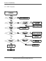
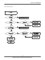
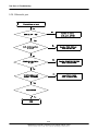
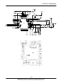
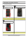
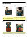
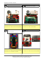
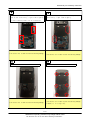
1
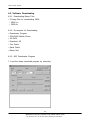
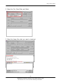
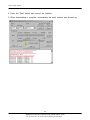
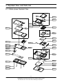
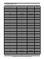
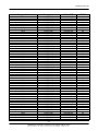
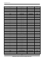
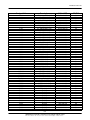
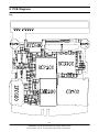
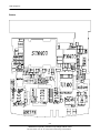
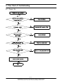
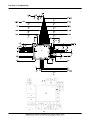
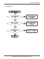
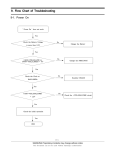
GSM TELEPHONE
SGH-G600
GSM TELEPHONE
CONTENTS
1.
Safety Precautions
2.
Specification
3.
Product Function
4.
Array course control
5.
Exploded View and Part List
6.
MAIN Electrical Parts List
7.
Block Diagrams
8.
PCB Diagrams
9.
Flow Chart of Troubleshooting
10.
Reference data
11.
Disassembly and Assembly
Instructions
GSPN (Global Service Partner Network)
Country
North America
Latin America
CIS
Europe
China
Asia
Mideast & Africa
Web Site
service.samsungportal.com
latin.samsungportal.com
cis.samsungportal.com
europe.samsungportal.com
china.samsungportal.com
asia.samsungportal.com
mea.samsungportal.com
This Service Manual is a property of Samsung Electronics Co.,Ltd.
Any unauthorized use of Manual can be punished under applicable
International and/or domestic law.
ⓒ Samsung Electronics Co.,Ltd.
2007. 08 Rev.1.0
1. Safety Precautions
1-1. Repair Precaution
― Repair in Shield Box, during detailed tuning.
Take specially care of tuning or test, because the
specification of cellular phone is sensitive for surrounding interference(RF noise).
― Be careful to use a kind of magnetic object or tool, because performance of parts is damaged by
the influence of magnetic force.
― Surely use a standard screwdriver when you disassemble this product, otherwise screw will be
worn away.
― Use a thicken twisted wire when you measure level.
A thicken twisted wire has low resistance,
therefore error of measurement is few.
― Repair after separate Test Pack and Set because for short danger (for example an overcurrent
and furious flames of parts etc) when you repair board in condition of connecting Test Pack and
tuning on.
― Take specially care of soldering, because Land of PCB is small and weak in heat.
― Surely tune on/off while using AC power plug, because a repair of battery charger is dangerous
when tuning ON/OFF PBA and Connector after disassembling charger.
― Don't use as you pleases after change other material than replacement registered on SEC System.
Otherwise engineer in charge isn't charged with problem that you don't keep this rules.
1-1
SAMSUNG Proprietary-Contents may change without notice
This Document can not be used without Samsung's authorization
Safety Precautions
1-2. ESD(Electrostatically Sensitive Devices) Precaution
Several semiconductor may be damaged easily by static electricity. Such parts are called by ESD
(Electrostatically Sensitive Devices), for example IC,BGA chip etc. Read Precaution below.
You can prevent from ESD damage by static electricity.
― Remove static electricity remained your body before you touch semiconductor or parts with
semiconductor. There are ways that you touch an earthed place or wear static electricity prevention
string on wrist.
― Use earthed soldering steel when you connect or disconnect ESD.
― Use soldering removing tool to break static electricity. , otherwise ESD will be damaged by static
electricity.
― Don't unpack until you set up ESD on product. Because most of ESD are packed by box and
aluminum plate to have conductive power,they are prevented from static electricity.
― You must maintain electric contact between ESD and place due to be set up until ESD is
connected completely to the proper place or a circuit board.
1-2
SAMSUNG Proprietary-Contents may change without notice
This Document can not be used without Samsung's authorization
2. Specification
2-1. GSM General Specification
G SM850
Pha se 1
G SM900
Pha se 1
EG SM 9 00
Pha se 2
DCS1800
PCS1900
Fr eq.
Band[MHz]
Uplin k/Down link
82 4~849
86 9~894
89 0~915
93 5~960
88 0~915
92 5~960
171 0~1785
180 5~1880
185 0~1910
193 0~1990
ARF CN ra nge
12 8~251
1 ~124
0~124 &
97 5~1023
51 2~885
51 2~810
T x/Rx spacing
4 5MHz
4 5MHz
4 5MHz
9 5MHz
8 0MHz
Mo d. Bit r ate/
Bit Period
270 .833kb ps
3. 692us
270 .833kb ps
3. 692us
270 .833kb ps
3. 692us
270 .833kb ps
3. 692us
270 .833kb ps
3. 692us
Ti me Slo t
Pe rio d/Fr am e
Per iod
57 6.9us
4.6 15ms
57 6.9us
4.6 15ms
57 6.9us
4.6 15ms
57 6.9us
4.6 15ms
57 6.9us
4.6 15ms
Modula tion
0. 3G MSK
0. 3G MSK
0. 3G MSK
0. 3G MSK
0. 3G MSK
MS Power
33d Bm~5dBm 33d Bm~5dBm 33d Bm~5dBm 30d Bm~0dBm 30d Bm~0dBm
Powe r Class
5pcl ~ 19pcl
5pcl ~ 19pcl
5pcl ~ 19pcl
0pcl ~ 15pcl
0pcl ~ 15pcl
Se nsitivity
-102 dBm
-102 dBm
-102 dBm
-100 dBm
-100 dBm
TDMA Mu x
8
8
8
8
8
Cell Radiu s
35Km
35Km
35Km
2Km
-
2-1
SAMSUNG Proprietary-Contents may change without notice
This Document can not be used without Samsung's authorization
Specification
2-2. GSM TX power class
TX Power
GSM850
GSM900
5
33±2 dBm
33±2 dBm
6
31±2 dBm
31±2 dBm
7
29±2 dBm
29±2 dBm
8
27±2 dBm
27±2 dBm
9
25±2 dBm
25±2 dBm
10
23±2 dBm
23±2 dBm
control level
11
12
13
14
15
16
21±2 dBm
19±2 dBm
17±2 dBm
15±2 dBm
13±2 dBm
11±3 dBm
TX Power
DCS1800
PCS1900
0
30±3 dBm
30±3 dBm
1
28±3 dBm
28±3 dBm
2
26±3 dBm
26±3 dBm
3
24±3 dBm
24±3 dBm
4
22±3 dBm
22±3 dBm
5
20±3 dBm
20±3 dBm
6
18±3 dBm
18±3 dBm
7
16±3 dBm
16±3 dBm
8
14±3 dBm
14±3 dBm
9
12±4 dBm
12±4 dBm
10
10±4 dBm
10±4 dBm
11
8±4dBm
8±4dBm
12
6±4 dBm
6±4 dBm
13
4±4 dBm
4±4 dBm
control level
21±2 dBm
19±2 dBm
17±2 dBm
15±2 dBm
13±2 dBm
11±3 dBm
17
9±3dBm
9±3dBm
18
7±3 dBm
7±3 dBm
14
2±5 dBm
2±5 dBm
19
5±3 dBm
5±3 dBm
15
0±5 dBm
0±5 dBm
2-2
SAMSUNG Proprietary-Contents may change without notice
This Document can not be used without Samsung's authorization
3. Product Function
Main Function
― DC-Jack TA (700mA)
― MMS (Multimedia Message Service)
― J2ME JAVA (MIDP 2.0/CLDC 1.1)
― EMS (Enhanced Message Service)
― 64 Poly S/W MIDI
― Bluetooth 2.0 EDR
― FM Radio Support
― USB v1.2 High Speed Support
― MicroSD Card Support
― Active backlight control
― Quad band(850/900/1800/1900MHz)
― GPRS Class 10
3-1
SAMSUNG Proprietary-Contents may change without notice
This Document can not be used without Samsung's authorization
Product Function
3-2
SAMSUNG Proprietary-Contents may change without notice
This Document can not be used without Samsung's authorization
4. Array course control
4-1. Software Adjustments
1.
2.
3.
4.
JIG Box(GH68-03306A): Download, Trace, Calibration, etc
RF test cable(GH39-00283A): RF test
Test cable(GH39-00838A): JIG to phone
Serial cable: PC to JIG
4-1
SAMSUNG Proprietary-Contents may change without notice
This Document can not be used without Samsung's authorization
Array course control
4-2. Software Downloading
4-2-1. Downloading Binary Files
• 2 binary files for downloading G600
– G600.cla
– G600.tfs
4-2-2. Pre-requsite for Downloading
• Downloader Program
• SGH-G600 Mobile Phone
• JIG BOX
• Download JIG
• Test Cable
• Serial Cable
• Binary files
4-2-3. S/W Downloader Program
1. Load the binary download program by executing
4-2
SAMSUNG Proprietary-Contents may change without notice
This Document can not be used without Samsung's authorization
Array course control
2. Select the Port, Baud Rate and Mode.
3. Select the binary files what you want to download
4-3
SAMSUNG Proprietary-Contents may change without notice
This Document can not be used without Samsung's authorization
Array course control
4. Press the "Start" button and connect the Handset
5. When downloading is complete, automatically the small window was showed up..
4-4
SAMSUNG Proprietary-Contents may change without notice
This Document can not be used without Samsung's authorization
Array course control
4-5
SAMSUNG Proprietary-Contents may change without notice
This Document can not be used without Samsung's authorization
5. Exploded View and Parts List
5-1. Cellular phone Exploded View
QFR04
QFR01
QCK01
QVO01
QCR57
QFU01
QKP01
QMW01
QMI03
QME01
QMI01
QBR03
QMP01
QKP02
QVK01
QCA01
QAN02
QLC01
QME03
QME02
QSH01
QMI04
QSP01
QSD01
QPC01
QRE01
QCR05
QIF01
QRF01
QFL01
QSC13
QBA01
QCR05
QSC05
QBA00
5-1
SAMSUNG Proprietary-Contents may change without notice
This Document can not be used without Samsung's authorization
Exploded View and Parts List
5-2. Cellular phone Parts list
Design LOC
Description
SEC CODE
QAN02
INTENNA-SGHG600
GH42-01290A
QBA00
PMO COVER-BATTERY
GH72-42760B
QBA01
INNER BATTERY PACK-880MAH , BL
GH43-02795A
QBR03
ASSY BRACKET-KEY
GH98-05613A
QCA01
CAMERA MODULE-5M
GH59-04643A
QCK01
PMO KEY-CAMERA
GH72-42790B
QCR05
SCREW-MACHINE
6001-001478
QCR05
SCREW-MACHINE
6001-001478
QCR57
SCREW-MACHINE
6001-002001
QFL01
ASSY CASE-SLIDE LOWER
GH98-05484B
QKP01
ASSY KEYPAD-MAIN(EU/E_BLK)
GH98-05489B
QKP02
ASSY KEYPAD-SUB(EU/E_BLK)
GH98-05488B
QLC01
MEA-LCD MODULE KIT
GH97-08026A
QME02
KEY FPCB-SUB KEY FPCB 10KEY
GH59-04700A
QME03
ASSY ETC-FLASH FPCB
GH59-04698A
QMP01
PBA MAIN-SGHG600
GH92-03873A
QPC01
MEA-FPCBKIT
GH97-08027A
QRF01
PMO COVER-RF
GH72-44462B
QSC05
RMO RUBBER-LOWER SCREW CAP
GH73-10563B
QSC13
RMO RUBBER-REAR SCREW CAP
GH73-10741B
QSH01
ICT COVER-SHIELD CAN
GH70-02732A
QSP01
UNIT-SGHG600,SPK MODULE
GH59-04704A
QVK01
KEY FPCB-VOLUME KEY
GH59-04706A
QVO01
PMO KEY-VOLUME
GH72-42793B
QME01
KEY FPCB-MAIN KEY FPCB 12 KEY
GH59-04699A
QMI01
AS-MIC SVC
GH81-06075A
QMI03
AS-SGHG600 MIC RUBBER
GH81-06836A
ASSY CASE-SLIDE UPPER
GH98-05483B
ASSY COVER-MAIN WINDOW
GH98-05487B
ASSY CASE-FRONT
GH98-05485B
ASSY DECO-FRONT
GH98-06134B
ASSY CASE-REAR
GH98-05486B
QIF01
PMO COVER-IF
GH72-42772B
QMI04
RMO RUBBER-PMIC
GH73-10901A
QSD01
PMO COVER-SD
GH72-42764B
QFU01
QMW01
QFR01
QFR04
QRE01
5-2
SAMSUNG Proprietary-Contents may change without notice
This Document can not be used without Samsung's authorization
Exploded View and Parts List
Description
SEC CODE
IC-MEMORY CARD
CONNECTOR-ADAPTOR
BAG PE
BAG ZIPPER
SCREW-MACHINE
MICROPHONE-ASSY-WEP210
CBF INTERFACE-MIC CABLE(S20P,B
CBF INTERFACE-DLC APCBS10BBE(S
BATTERY-70MAH CORE PACK
ADAPTOR-ATADS10UBE,BLK,UK
S/W CD-SGH-G600 SAMSUNG PC STU
KEY FPCB-SIDE KEY
EARPHONE-EARPHONE,3 PLUG,BLK,E
ASSY ETC-CONVERSION PLUG
LABEL(P)-UNIT SEAL
LABEL(P)-IMEI
MANUAL-SFC LEAFLET
LABEL(R)-WATER SOAK
MANUAL USERS-EU ENGLISH
LABEL(R)-MAIN(EU)
MANUAL USERS-EU ENGLISH
BOX-UNIT(UK)
CUSHION-CASE(UK)
PMO DECO-UPPER TOP
PMO COVER-DC JACK
PMO-VOL KEY V2
PMO CASE-EARPIECE
RMO-EAR RUBBER 1
RMO-EAR RUBBER 4
RMO-RUBBER MIC
RMO-RUBBER SCREW
RMO RUBBER-CHIP
MPR-CONN REMOVLA TAPE
MPR-TAPE MAIN KEY SOLDERING
MPR-INSU TAPE TOUCH CONN
MPR-SPONGE BATT
MPR-SPONGE MIC
TAPE-SPK CONN
TAPE-SLIDE CONN 2
TAPE ELEC
TAPE ELEC
TAPE INSU-SUB FPCB
TAPE INSU
TAPE-ABSORBER CHIP
VINYL-BOHO WINDOW MAIN END
SPONGE
TAPE ELEC
PBA MAIN-IN HOUSE
ELA UNIT-WEP210, EBONY GRAY(EU
ASSY CASE-UPPER
ASSY CASE-LOWER
1109-001363
3719-001319
6902-000634
6902-000683
6001-001478
GH30-00312A
GH39-00913A
GH39-00922A
GH43-02683A
GH44-01756A
GH46-00490A
GH59-03784A
GH59-04418A
GH59-04444A
GH68-00518B
GH68-01335D
GH68-04822A
GH68-09361A
GH68-15425A
GH68-15559A
GH68-15785A
GH69-05703G
GH69-05706A
GH72-35348C
GH72-35353C
GH72-35354A
GH72-35513C
GH73-08109A
GH73-08112A
GH73-08425A
GH73-08831A
GH73-10900A
GH74-04200A
GH74-22250A
GH74-27252A
GH74-27787A
GH74-27788A
GH74-33771A
GH74-33773A
GH74-33928A
GH74-33929A
GH74-34636A
GH74-34638A
GH74-34639A
GH74-34806A
GH74-34853A
GH74-34894A
GH92-03339A
GH96-02761A
GH98-02765D
GH98-02766C
5-3
SAMSUNG Proprietary-Contents may change without notice
This Document can not be used without Samsung's authorization
Exploded View and Parts List
5-4
SAMSUNG Proprietary-Contents may change without notice
This Document can not be used without Samsung's authorization
6. Electrical Parts List
Design LOC
Description
SEC CODE
STATUS
ANT101
ANT102
BAT400
BTC600
C100
C101
C101
C102
C102
C103
C103
C104
C104
C105
C105
C106
C106
C107
C107
C108
C108
C109
C109
C110
C110
C111
C111
C112
C112
C113
C114
C114
C115
C116
C117
C117
C118
C119
C119
C120
C120
C121
C122
C123
C123
C124
C125
C126
C127
C128
C129
C130
C131
C132
C133
C134
ANTENNA-CHIP
ANTENNA-CHIP
BATTERY-LI(2ND)
HEADER-BATTERY
C-CER,CHIP
C-CER,CHIP
C-CER,CHIP
C-CER,CHIP
C-CER,CHIP
C-CER,CHIP
C-CER,CHIP
C-CER,CHIP
C-CER,CHIP
C-CER,CHIP
C-CER,CHIP
C-CER,CHIP
C-CER,CHIP
C-CER,CHIP
C-CER,CHIP
C-CER,CHIP
C-CER,CHIP
C-CER,CHIP
C-CER,CHIP
C-CER,CHIP
C-CER,CHIP
C-CER,CHIP
C-CER,CHIP
C-CER,CHIP
C-CER,CHIP
C-TA,CHIP
C-CER,CHIP
C-CER,CHIP
C-CER,CHIP
C-CER,CHIP
C-CER,CHIP
C-CER,CHIP
C-CER,CHIP
C-CER,CHIP
C-CER,CHIP
C-CER,CHIP
C-CER,CHIP
C-CER,CHIP
C-CER,CHIP
C-CER,CHIP
C-CER,CHIP
C-CER,CHIP
C-CER,CHIP
C-CER,CHIP
C-CER,CHIP
C-CER,CHIP
C-CER,CHIP
C-CER,CHIP
C-CER,CHIP
C-CER,CHIP
C-CER,CHIP
C-CER,CHIP
4202-001254
4202-001255
4302-001181
3711-006217
2203-000233
2203-005281
2203-006824
2203-001385
2203-006194
2203-002982
2203-005281
2203-002982
2203-005281
2203-005281
2203-005729
2203-005446
2203-006647
2203-000278
2203-006647
2203-000812
2203-006824
2203-005736
2203-006647
2203-005729
2203-005736
2203-005446
2203-006194
2203-000254
2203-005736
2404-001496
2203-000812
2203-006838
2203-001385
2203-000628
2203-005281
2203-005288
2203-002668
2203-005288
2203-006439
2203-000330
2203-006305
2203-002709
2203-006305
2203-000233
2203-006260
2203-006562
2203-006562
2203-006048
2203-006994
2203-005482
2203-002709
2203-006838
2203-000438
2203-006423
2203-006423
2203-000438
SA
SA
SA
SA
SA
SA
SA
SA
SA
SA
SA
SA
SA
SA
SA
SA
SA
SA
SA
SA
SA
SA
SA
SA
SA
SA
SA
SA
SA
SA
SA
SA
SA
SA
SA
SA
SA
SA
SNA
SA
SA
SA
SA
SA
SA
SA
SA
SA
SA
SA
SA
SA
SA
SA
SA
SA
6-1
SAMSUNG Proprietary-Contents may change without notice
This Document can not be used without Samsung's authorization
Electrical Parts List
Design LOC
Description
SEC CODE
STATUS
C135
C136
C137
C138
C139
C140
C200
C201
C202
C203
C204
C205
C206
C207
C208
C209
C210
C211
C212
C213
C214
C215
C216
C217
C218
C219
C220
C300
C301
C302
C303
C304
C305
C306
C307
C308
C309
C310
C312
C313
C314
C315
C316
C317
C318
C319
C320
C321
C322
C323
C324
C325
C326
C327
C400
C401
C-CER,CHIP
C-CER,CHIP
C-CER,CHIP
C-CER,CHIP
C-CER,CHIP
C-CER,CHIP
C-CER,CHIP
C-CER,CHIP
C-CER,CHIP
C-CER,CHIP
C-CER,CHIP
C-CER,CHIP
C-CER,CHIP
C-CER,CHIP
C-CER,CHIP
C-CER,CHIP
C-CER,CHIP
C-CER,CHIP
C-CER,CHIP
C-CER,CHIP
C-CER,CHIP
C-CER,CHIP
C-CER,CHIP
C-CER,CHIP
C-CER,CHIP
C-CER,CHIP
C-CER,CHIP
C-CER,CHIP
C-CER,CHIP
C-CER,CHIP
C-CER,CHIP
C-CER,CHIP
C-CER,CHIP
C-CER,CHIP
C-CER,CHIP
C-CER,CHIP
C-CER,CHIP
C-CER,CHIP
C-CER,CHIP
C-CER,CHIP
C-CER,CHIP
C-CER,CHIP
C-CER,CHIP
C-CER,CHIP
C-CER,CHIP
C-CER,CHIP
C-CER,CHIP
C-CER,CHIP
C-CER,CHIP
C-CER,CHIP
C-CER,CHIP
C-CER,CHIP
C-CER,CHIP
C-CER,CHIP
C-CER,CHIP
C-CER,CHIP
2203-000438
2203-002668
2203-006838
2203-006423
2203-000278
2203-006842
2203-005482
2203-000812
2203-005482
2203-005482
2203-005482
2203-005482
2203-005482
2203-006423
2203-005482
2203-000254
2203-005482
2203-005682
2203-006423
2203-006423
2203-006399
2203-006423
2203-006423
2203-006399
2203-006562
2203-000425
2203-000425
2203-006423
2203-006423
2203-006423
2203-006423
2203-006423
2203-006423
2203-006423
2203-006423
2203-006423
2203-006562
2203-006562
2203-006048
2203-006048
2203-006048
2203-006048
2203-006423
2203-006423
2203-006423
2203-006423
2203-006423
2203-006324
2203-006208
2203-006048
2203-006260
2203-006121
2203-000330
2203-000330
2203-006257
2203-006208
SA
SA
SA
SA
SA
SA
SA
SA
SA
SA
SA
SA
SA
SA
SA
SA
SA
SA
SA
SA
SA
SA
SA
SA
SA
SA
SA
SA
SA
SA
SA
SA
SA
SA
SA
SA
SA
SA
SA
SA
SA
SA
SA
SA
SA
SA
SA
SA
SA
SA
SA
SA
SA
SA
SA
SA
6-2
SAMSUNG Proprietary-Contents may change without notice
This Document can not be used without Samsung's authorization
Electrical Parts List
Design LOC
Description
SEC CODE
STATUS
C402
C403
C404
C405
C406
C407
C408
C409
C410
C411
C412
C413
C414
C418
C419
C420
C421
C422
C423
C424
C425
C426
C427
C501
C502
C504
C505
C506
C507
C508
C509
C510
C511
C512
C514
C515
C516
C517
C519
C520
C521
C523
C524
C525
C526
C527
C600
C601
C602
C603
C604
C605
C609
C610
C612
C614
C-CER,CHIP
C-CER,CHIP
C-CER,CHIP
C-CER,CHIP
C-CER,CHIP
C-CER,CHIP
C-CER,CHIP
C-CER,CHIP
C-CER,CHIP
C-CER,CHIP
C-CER,CHIP
C-CER,CHIP
C-CER,CHIP
C-CER,CHIP
C-CER,CHIP
C-CER,CHIP
C-CER,CHIP
C-CER,CHIP
C-CER,CHIP
C-CER,CHIP
C-CER,CHIP
C-CER,CHIP
C-CER,CHIP
C-CER,CHIP
C-CER,CHIP
C-CER,CHIP
C-CER,CHIP
C-CER,CHIP
C-CER,CHIP
C-CER,CHIP
C-CER,CHIP
C-CER,CHIP
C-CER,CHIP
C-CER,CHIP
C-CER,CHIP
C-CER,CHIP
C-CER,CHIP
C-CER,CHIP
C-CER,CHIP
C-CER,CHIP
C-CER,CHIP
C-CER,CHIP
C-CER,CHIP
C-CER,CHIP
C-CER,CHIP
C-CER,CHIP
C-CER,CHIP
C-CER,CHIP
C-CER,CHIP
C-CER,CHIP
C-CER,CHIP
C-CER,CHIP
C-CER,CHIP
C-CER,CHIP
C-CER,CHIP
C-CER,CHIP
2203-006257
2203-006257
2203-006208
2203-006257
2203-006208
2203-006257
2203-006257
2203-000233
2203-000425
2203-006348
2203-006562
2203-000425
2203-005482
2203-006257
2203-006324
2203-005482
2203-006208
2203-006562
2203-006201
2203-006361
2203-006474
2203-006562
2203-006562
2203-005482
2203-005482
2203-006399
2203-006399
2203-005993
2203-006399
2203-005993
2203-006399
2203-006562
2203-006562
2203-005482
2203-005482
2203-005482
2203-000386
2203-000386
2203-005482
2203-001259
2203-005482
2203-006562
2203-006260
2203-006260
2203-006260
2203-006260
2203-000425
2203-001437
2203-001259
2203-000995
2203-001437
2203-000425
2203-006423
2203-006896
2203-005061
2203-005482
SA
SA
SA
SA
SA
SA
SA
SA
SA
SA
SA
SA
SA
SA
SA
SA
SA
SA
SA
SA
SA
SA
SA
SA
SA
SA
SA
SA
SA
SA
SA
SA
SA
SA
SA
SA
SA
SA
SA
SA
SA
SA
SA
SA
SA
SA
SA
SA
SA
SA
SA
SA
SA
SA
SA
SA
6-3
SAMSUNG Proprietary-Contents may change without notice
This Document can not be used without Samsung's authorization
Electrical Parts List
Design LOC
Description
SEC CODE
STATUS
C615
C617
C618
C619
C620
C702
C704
C705
C706
C707
C708
C709
C710
C711
C712
C713
C714
C715
C717
C718
C719
C720
C721
C722
C723
C724
C725
C726
C728
C729
C730
C731
C732
CD700
CN100
CON101
D101
D600
D601
D602
D603
D604
D605
D700
D701
D702
D703
D704
D705
F100
F101
F101
F600
HDC700
HDC701
IFC600
C-CER,CHIP
C-CER,CHIP
C-CER,CHIP
C-CER,CHIP
C-CER,CHIP
C-CER,CHIP
C-CER,CHIP
C-CER,CHIP
C-CER,CHIP
C-CER,CHIP
C-CER,CHIP
C-CER,CHIP
C-CER,CHIP
C-CER,CHIP
C-CER,CHIP
C-CER,CHIP
C-CER,CHIP
C-CER,CHIP
C-CER,CHIP
C-CER,CHIP
C-CER,CHIP
C-CER,CHIP
C-CER,CHIP
C-CER,CHIP
C-CER,CHIP
C-CER,CHIP
C-CER,CHIP
C-CER,CHIP
C-CER,CHIP
C-CER,CHIP
C-CER,CHIP
C-CER,CHIP
C-CER,CHIP
CONNECTOR-CARD EDGE
CONNECTOR-COAXIAL
JACK-DC POWER
DIODE-ZENER
DIODE-TVS
DIODE-TVS
DIODE-TVS
DIODE-TVS
DIODE-TVS
DIODE-TVS
DIODE-TVS
DIODE-TVS
DIODE-TVS
DIODE-TVS
DIODE-TVS
DIODE-TVS
DUPLEXER-FEM
FILTER-LC
FILTER-LC
FILTER-EMI SMD
HEADER-BOARD TO BOARD
HEADER-BOARD TO BOARD
SOCKET-INTERFACE
2203-000254
2203-006423
2203-000233
2203-000995
2203-000679
2203-000386
2203-006562
2203-006562
2203-006399
2203-000812
2203-005682
2203-005682
2203-005682
2203-005682
2203-005682
2203-005682
2203-005682
2203-006562
2203-005682
2203-005682
2203-005682
2203-005682
2203-005682
2203-005682
2203-005682
2203-005682
2203-005682
2203-005682
2203-000812
2203-005682
2203-005682
2203-005682
2203-005682
3709-001464
3705-001358
3722-002433
0403-001547
0406-001208
0406-001208
0406-001231
0406-001231
0406-001231
0406-001203
0406-001208
0406-001208
0406-001223
0406-001223
0406-001223
0406-001223
2911-000076
2909-001279
2909-001283
2901-001408
3711-006326
3711-006593
3710-002523
SA
SA
SA
SA
SA
SA
SA
SA
SA
SA
SA
SA
SA
SA
SA
SA
SA
SA
SA
SA
SA
SA
SA
SA
SA
SA
SA
SA
SA
SA
SA
SA
SA
SA
SA
SA
SA
SA
SA
SA
SA
SA
SA
SA
SA
SA
SA
SA
SA
SA
SA
SA
SA
SA
SA
SA
6-4
SAMSUNG Proprietary-Contents may change without notice
This Document can not be used without Samsung's authorization
Electrical Parts List
Design LOC
Description
SEC CODE
STATUS
L100
L101
L101
L102
L102
L103
L103
L104
L104
L105
L106
L107
L108
L110
L111
L112
L113
L115
L116
L117
L300
L301
L401
L500
L501
L503
L505
L506
L601
L602
L603
L605
L606
OSC100
OSC101
OSC300
OSC400
PAM500
PM400
Q100
QCR05
QCR05
QCR05
QCR57
R100
R101
R101
R102
R102
R103
R104
R104
R105
R105
R106
R106
ICT-ON-BOARD CLIP
INDUCTOR-SMD
ICT-ON-BOARD CLIP
INDUCTOR-SMD
ICT-ON-BOARD CLIP
INDUCTOR-SMD
ICT-ON-BOARD CLIP
INDUCTOR-SMD
ICT-ON-BOARD CLIP
ICT-ON-BOARD CLIP
INDUCTOR-SMD
INDUCTOR-SMD
INDUCTOR-SMD
INDUCTOR-SMD
INDUCTOR-SMD
INDUCTOR-SMD
INDUCTOR-SMD
BEAD-SMD
BEAD-SMD
INDUCTOR-SMD
INDUCTOR-SMD
INDUCTOR-SMD
INDUCTOR-SMD
BEAD-SMD
BEAD-SMD
BEAD-SMD
BEAD-SMD
BEAD-SMD
BEAD-SMD
BEAD-SMD
BEAD-SMD
INDUCTOR-SMD
INDUCTOR-SMD
CRYSTAL-SMD
CRYSTAL-SMD
CRYSTAL-SMD
CRYSTAL-SMD
IC-AUDIO AMP
IC-POWER SUPERVISOR
FET-SILICON
SCREW-MACHINE
SCREW-MACHINE
SCREW-MACHINE
SCREW-MACHINE
R-CHIP
R-CHIP
R-CHIP
R-CHIP
R-CHIP
R-CHIP
R-CHIP
R-CHIP
R-CHIP
R-CHIP
R-CHIP
R-CHIP
GH70-02367A
2703-002901
GH70-02367A
2703-003095
GH70-02367A
2703-002795
GH70-02367A
2703-002649
GH70-02367A
GH70-02367A
2703-002208
2703-002281
2703-002314
2703-002558
2703-002558
2703-002608
2703-002608
3301-001534
3301-001659
2703-002198
2703-002866
2703-001231
2703-002861
3301-001729
3301-001729
3301-001438
3301-001438
3301-001812
3301-001812
3301-001812
3301-001812
2703-002910
2703-001673
2801-004426
2801-004568
2801-004285
2801-004339
1201-002492
1203-004382
0505-002088
6001-001478
6001-001478
6001-001478
6001-002001
2007-000140
2007-000566
2007-008056
2007-000143
2007-009108
2007-008516
2007-000162
2007-008516
2007-000162
2007-008516
2007-007489
2007-008516
SA
SNA
SA
SA
SA
SNA
SA
SNA
SA
SA
SA
SA
SA
SA
SA
SA
SA
SA
SA
SA
SA
SNA
SA
SA
SA
SA
SA
SA
SA
SA
SA
SA
SA
SA
SA
SA
SA
SA
SA
SA
SA
SA
SA
SA
SA
SA
SA
SA
SA
SA
SA
SA
SA
SA
SA
SA
6-5
SAMSUNG Proprietary-Contents may change without notice
This Document can not be used without Samsung's authorization
Electrical Parts List
Design LOC
Description
SEC CODE
STATUS
R107
R108
R109
R110
R111
R112
R113
R115
R116
R117
R118
R119
R120
R121
R122
R123
R203
R204
R205
R206
R207
R208
R209
R210
R211
R212
R305
R307
R308
R311
R313
R316
R317
R318
R319
R322
R323
R324
R325
R326
R400
R402
R403
R408
R410
R411
R412
R413
R414
R415
R416
R417
R501
R502
R503
R504
R-CHIP
R-CHIP
R-CHIP
R-CHIP
R-CHIP
R-CHIP
R-CHIP
R-CHIP
R-CHIP
R-CHIP
R-CHIP
R-CHIP
R-CHIP
R-CHIP
R-CHIP
R-CHIP
R-CHIP
R-CHIP
R-CHIP
R-CHIP
R-CHIP
R-CHIP
R-CHIP
R-CHIP
R-CHIP
R-CHIP
R-CHIP
R-CHIP
R-CHIP
R-CHIP
R-CHIP
R-CHIP
R-CHIP
R-CHIP
R-CHIP
R-CHIP
R-CHIP
R-CHIP
R-CHIP
R-CHIP
R-CHIP
R-CHIP
BEAD-SMD
R-CHIP
R-CHIP
R-CHIP
R-CHIP
R-CHIP
R-CHIP
R-CHIP
R-CHIP
R-CHIP
R-CHIP
R-CHIP
R-CHIP
R-CHIP
2007-001316
2007-008056
2007-000141
2007-008420
2007-008420
2007-003015
2007-008516
2007-000148
2007-008544
2007-008544
2007-000566
2007-000163
2007-003015
2007-000148
2007-000566
2007-000171
2007-000148
2007-000758
2007-009314
2007-008419
2007-008055
2007-000148
2007-001319
2007-001319
2007-008055
2007-000148
2007-008045
2007-003013
2007-003013
2007-008478
2007-001290
2007-001290
2007-009084
2007-009084
2007-008055
2007-007316
2007-000170
2007-000162
2007-007009
2007-001156
2007-007573
2007-008354
3301-001659
2007-000171
2007-001333
2007-007311
2007-000141
2007-000162
2007-002796
2007-000162
2007-000758
2007-000162
2007-008542
2007-008420
2007-008420
2007-000157
SA
SA
SA
SA
SA
SA
SA
SA
SA
SA
SA
SA
SA
SA
SA
SA
SA
SA
SA
SA
SA
SA
SA
SA
SA
SA
SA
SA
SA
SA
SA
SA
SA
SA
SA
SA
SA
SA
SA
SA
SA
SA
SA
SA
SA
SA
SA
SA
SA
SA
SA
SA
SA
SA
SA
SA
6-6
SAMSUNG Proprietary-Contents may change without notice
This Document can not be used without Samsung's authorization
Electrical Parts List
Design LOC
Description
SEC CODE
STATUS
R507
R508
R509
R510
R511
R512
R513
R514
R515
R600
R601
R602
R603
R604
R606
R607
R608
R609
R610
R611
R612
R700
R701
R703
R704
R705
R706
R707
R708
R709
R712
R713
SIM400
TA101
TA300
TA400
TA401
TA500
TA501
TA502
TA503
TA504
TA505
TA506
TA507
TA600
TA601
U100
U101
U101
U102
U103
U104
U300
U301
U302
R-CHIP
R-CHIP
R-CHIP
R-CHIP
R-CHIP
R-CHIP
R-CHIP
R-CHIP
R-CHIP
R-CHIP
R-CHIP
R-CHIP
R-CHIP
R-CHIP
R-CHIP
R-CHIP
R-CHIP
R-CHIP
R-CHIP
BEAD-SMD
R-CHIP
R-CHIP
R-CHIP
R-CHIP
R-CHIP
R-CHIP
R-CHIP
R-CHIP
R-CHIP
R-CHIP
R-CHIP
R-CHIP
CONNECTOR-CARD EDGE
C-TA,CHIP
C-TA,CHIP
C-TA,CHIP
C-TA,CHIP
C-TA,CHIP
C-TA,CHIP
C-TA,CHIP
C-TA,CHIP
C-TA,CHIP
C-TA,CHIP
C-TA,CHIP
C-TA,CHIP
C-TA,CHIP
C-TA,CHIP
IC-POWER AMP
IC-POSI.FIXED REG.
IC-DATA COMM./GEN.
IC-TRANSCEIVER
IC-CMOS LOGIC
IC-TRANSCEIVER
IC-POSI.FIXED REG.
IC-DC/DC CONVERTER
IC-ANALOG MULTIPLEX
2007-007528
2007-000171
2007-007528
2007-000148
2007-007528
2007-007528
2007-002796
2007-000140
2007-002796
2007-009170
2007-007107
2007-009112
2007-007741
2007-007334
2007-001333
2007-007741
2007-008800
2007-000162
2007-000162
3301-001917
2007-000148
2007-009112
2007-000159
2007-000159
2007-000159
2007-000159
2007-000157
2007-000165
2007-000166
2007-008055
2007-000143
2007-000143
3709-001447
2404-001381
2404-001381
2404-001381
2404-001225
2404-001396
2404-001396
2404-001430
2404-001226
2404-001414
2404-001225
2404-001414
2404-001225
2404-001381
2404-001381
1201-002423
1203-003688
1205-002748
1205-003093
0801-003012
1205-002942
1203-003737
1203-004548
1001-001472
SA
SA
SA
SA
SA
SA
SA
SA
SA
SA
SA
SNA
SA
SA
SA
SA
SA
SA
SA
SA
SA
SNA
SA
SA
SA
SA
SA
SA
SA
SA
SA
SA
SA
SA
SA
SA
SA
SA
SA
SA
SA
SA
SA
SA
SA
SA
SA
SA
SA
SA
SA
SA
SA
SA
SA
SA
6-7
SAMSUNG Proprietary-Contents may change without notice
This Document can not be used without Samsung's authorization
Electrical Parts List
Design LOC
Description
SEC CODE
STATUS
U401
U402
U500
U501
U503
U504
U600
U601
U700
UCD300
UCD500
UCP200
UME200
UPL200
UPL700
V601
VR101
VR102
VR103
VR104
VR105
VR106
VR107
VR110
VR600
ZD101
ZD600
ZD601
ZD602
ZD603
ZD604
ZD605
IC-POSI.FIXED REG.
IC-POSI.FIXED REG.
IC-POSI.FIXED REG.
IC-ANALOG MULTIPLEX
IC-ANALOG MULTIPLEX
IC-ANALOG MULTIPLEX
IC-ANALOG SWITCH
IC-DEMODULATOR
IC-POSI.FIXED REG.
IC ASIC-SGHG600
IC-CODEC
IC-COMM. CONTROLLER
IC-MCP
IC-CMOS LOGIC
FET-SILICON
VARISTOR
VARISTOR
VARISTOR
VARISTOR
VARISTOR
VARISTOR
VARISTOR
VARISTOR
VARISTOR
THERMISTOR-NTC
DIODE-SCHOTTKY
DIODE-ZENER
DIODE-TVS
DIODE-TVS
DIODE-TVS
DIODE-TVS
DIODE-TVS
1203-003737
1203-003737
1203-003737
1001-001447
1001-001349
1001-001447
1001-001394
1204-002688
1203-003815
GH13-00059A
1205-003214
1205-003082
1108-000112
0801-003022
0505-002111
1405-001183
1405-001082
1405-001082
1405-001093
1405-001082
1405-001082
1405-001082
1405-001093
1405-001167
1404-001221
0404-001172
0403-001547
0406-001254
0406-001267
0406-001267
0406-001223
0406-001223
SA
SA
SA
SA
SA
SA
SA
SA
SA
SA
SA
SA
SA
SA
SA
SA
SA
SA
SA
SA
SA
SA
SA
SA
SA
SA
SA
SA
SA
SA
SA
SA
6-8
SAMSUNG Proprietary-Contents may change without notice
This Document can not be used without Samsung's authorization
7. Block Diagrams
7-1. RF Solution Block Diagram
7-1
SAMSUNG Proprietary-Contents may change without notice
This Document can not be used without Samsung's authorization
Block Diagrams
7-2. BT Solution Block Diagram
7-2
SAMSUNG Proprietary-Contents may change without notice
This Document can not be used without Samsung's authorization
Block Diagrams
7-3. Base Band Solution Block Diagram
MIC
BB INTERFACE
Serial Data
Interface
RECEIVER
SPEAKER
Ext.
SPEAKER
VIBRATOR
PCF5213EL1
Battery
Type
Battery
Voltage
I/O
Interface
Battery
Temperature
A/D
Interface
D1VDD
D2VDD
MELODY IC
(64 Poly)
D3VDD
RF INTERFACE
AVDD
SYSTEM CLOCK
(26MHz)
AFC
VINT
IOVDD
MV319DNQ
RAMP
VDD_RX_TX
VCC_SYN
1G OneNAND
MEMORY
MIC_BIAS
Li-Ion Battery
(Slim,Standard)
CPVDD
PMU
SIMEN
KEY_BOARD
GPO
LCD
Charging Circuit
RTC_CLOCK
(32.768KHz)
VCHG
SIM CARD
VSAVE
7-3
SAMSUNG Proprietary-Contents may change without notice
This Document can not be used without Samsung's authorization
8. PCB Diagrams
Top
8-1
SAMSUNG Proprietary-Contents may change without notice
This Document can not be used without Samsung's authorization
PCB Diagrams
Bottom
8-2
SAMSUNG Proprietary-Contents may change without notice
This Document can not be used without Samsung's authorization
9. Flow Chart of Troubleshooting
9-1. Power On
' Power On ' does not work
Yes
Check the Battery Voltage
No
Change the Battery
is more than 3.7V
Yes
No
Check the PMU related to VISA
C418(VISA) = 2.6V?
Yes
Check the Clock at
No
Resolder OSC400
R409=32KHZ
Yes
C400(+VDD_IO_LOW) &
C402(+VDD_IO_HIGH) = "H"?
No
Check the related circuit
Yes
C425(+VDD_GSM_CORE)
No
Check the +VDD_GSM_CORE circuit
= 1.2V?
Yes
Check the initial operation
Yes
END
9-1
SAMSUNG Proprietary-Contents may change without notice
This Document can not be used without Samsung's authorization
Flow Chart of Troubleshooting
9-2
SAMSUNG Proprietary-Contents may change without notice
This Document can not be used without Samsung's authorization
Flow Chart of Troubleshooting
9-2. Initial
Initial Failure
Yes
No
UCP200 pin C11 (RSTON) ="H"?
Check the circuit related to reset
Yes
No
UCP200 pin
F1(RSTEXTn) ="H"?
change UCP200
OK?
Yes
Check the 16bit data signal
& memory CE
Yes
END
9-3
SAMSUNG Proprietary-Contents may change without notice
This Document can not be used without Samsung's authorization
Flow Chart of Troubleshooting
9-4
SAMSUNG Proprietary-Contents may change without notice
This Document can not be used without Samsung's authorization
Flow Chart of Troubleshooting
9-3. Charging Part
Abnormal charging part
Yes
No
Check the PM400 pin 38
Check the circuit related to
V_EXT_CHARGE
> 5.0V
Yes
No
PM400 pin 34(AUX_ON)
Check the circuit related to
AUX_ON signal
= "L"?
Yes
No
Check the PM400 pin 36
Resolder or replace PM400
≒ 1.25V
Yes
END
9-5
SAMSUNG Proprietary-Contents may change without notice
This Document can not be used without Samsung's authorization
Flow Chart of Troubleshooting
9-6
SAMSUNG Proprietary-Contents may change without notice
This Document can not be used without Samsung's authorization
Flow Chart of Troubleshooting
9-4. Sim Part
Phone can't access SIM Card
Yes
No
SIM400 pin 1,5 = "H"?
Resolder or replace PM400
Yes
No
After Power ON,
Check SIMCLK Signal on
Check the Clock
pin3 of SIM400 in a few second
Yes
No
After SIM card insert,
Replace PBA
SIM400 pin 2 = "H(SIM_RST)"?
Yes
Check the SIM Card
Yes
END
9-7
SAMSUNG Proprietary-Contents may change without notice
This Document can not be used without Samsung's authorization
Flow Chart of Troubleshooting
9-8
SAMSUNG Proprietary-Contents may change without notice
This Document can not be used without Samsung's authorization
Flow Chart of Troubleshooting
9-5. Microphone Part
Microphone does not work
Yes
No
Check the connection
Replace the MIC FPCB
from MIC FPCB
Yes
Check the circuit
No
Resolder the U503, C519, C521, R509, R512
from UCP200 to MIC
FPCB
Yes
END
9-9
SAMSUNG Proprietary-Contents may change without notice
This Document can not be used without Samsung's authorization
Flow Chart of Troubleshooting
9-10
SAMSUNG Proprietary-Contents may change without notice
This Document can not be used without Samsung's authorization
Flow Chart of Troubleshooting
9-6. Speaker Part(Melody)
Speaker does not work
No
PAM500 pin15,17 ≒ 1.8V?
Resolder PAM500
(When PAM500 operate)
Yes
No
Is Speaker working?
Change the Speaker
Yes
END
9-11
SAMSUNG Proprietary-Contents may change without notice
This Document can not be used without Samsung's authorization
Flow Chart of Troubleshooting
9-12
SAMSUNG Proprietary-Contents may change without notice
This Document can not be used without Samsung's authorization
Flow Chart of Troubleshooting
9-7. Key Data Input
Check Initial Operation
Yes
When one of the keys is
No
Check the Dome sheet & Key Pad
pushed,
is it displayed on LCD?
Yes
When one of the keys is
No
Replace the Key PBA
pushed,
KBIO signal is OK?
Yes
END
9-13
SAMSUNG Proprietary-Contents may change without notice
This Document can not be used without Samsung's authorization
Flow Chart of Troubleshooting
9-8. Back Light (for Color Main LCD)
Backlight does not work
Yes
No
Is LCD Contrast set on high
Set LCD Contrast on high level
level in the Menu?
Yes
No
Change the Slide FPCB or LCD
Check the Slide FPCB
Yes
END
9-14
SAMSUNG Proprietary-Contents may change without notice
This Document can not be used without Samsung's authorization
Flow Chart of Troubleshooting
9-9. Key Back Light
Main Key LED does not work
Yes
No
Check the key FPCB
connector on PBA
Reconnect the key FPCB
Yes
IS key FPCB ok?
Change key FPCB
END
9-15
SAMSUNG Proprietary-Contents may change without notice
This Document can not be used without Samsung's authorization
Flow Chart of Troubleshooting
9-10. Camera part
"Camera" function does not work
Yes
No
Check the Camera
Reconnect the camera module
connector on PBA
Yes
Is there another problem?
Yes
Replace the camera
module
END
9-16
SAMSUNG Proprietary-Contents may change without notice
This Document can not be used without Samsung's authorization
Flow Chart of Troubleshooting
9-11. Radio part
Radio does not work
Yes
No
Resolder R613
R613
≥ 2.8V
and Check PMU part
Yes
No
R610, R612, C614, C615
≥ 2.8V
Resolder R610, R612, C614, C615
and check U601
Yes
No
L605 ≥ 2V
Check or Replace U601
Yes
No
C618, C619, C620, L606
is OK?
(When U601 operate)
Resolder C618, C619, C620, L606
Yes
Check UCP200 signal
related to U601
Yes
END
9-17
SAMSUNG Proprietary-Contents may change without notice
This Document can not be used without Samsung's authorization
Flow Chart of Troubleshooting
9-18
SAMSUNG Proprietary-Contents may change without notice
This Document can not be used without Samsung's authorization
Flow Chart of Troubleshooting
9-12. GSM Receiver
RX ON
Cell Power : -60dBm
Yes
No
F100 Pin11
≥ -65dBm
Resolder CN100,C102,L109
Yes
No
F100 3,4
≥ -68dBm
No
Check F100
pin10,pin14 = L
Check ANT Switch
control circuit
Yes
Resolder F100
Yes
No
U102
pin 24 ≥ -70dBm
pin 25 ≥ -70dBm
Resolder C104, C105, L111
Yes
U102 pin 4,5,6,7
≥ 0.2Vp_p
No
U102pin 11,12,16,
29,32,33,36 ≥2.8V
pin10≥1.8V
No
Check & Resolder
C122,C126,C128
And PMU Part
Yes
Yes
Resolder U102
Check UCP200
END
9-19
SAMSUNG Proprietary-Contents may change without notice
This Document can not be used without Samsung's authorization
Flow Chart of Troubleshooting
9-13. GSM Transmitter
TX ON (5Level)
Yes
Yes
F100 Pin11
≥ 30dBm
Resolder CN100,C102,L109
No
Yes
F100 pin17
≥ 30dBm
Check F100
pin14 = H (2.6V),
Pin10 = L
No
Check ANT Switch
control circuit
Yes
No
Change or Resolder F100
Yes
U100 pin12
≥ 30dBm
Resolder or Change C120,
C121, L114
No
Yes
U100 pin7
≥ -4dBm
Check U100 pin
2,3,5,6,8, +Vbatt
pin4OK?
Yes
Resolder or Change U100
No
Check VBAT or PAM
control signal
No
Yes
U102 pin 4,5,6,7
≥ 0.2Vp_p
U102pin 11,12,16,
29,32,33,36 ≥2.8V
pin10≥1.8V
No
No
Yes
Check UCP200
END
9-20
SAMSUNG Proprietary-Contents may change without notice
This Document can not be used without Samsung's authorization
Check U102,
C122,C126,C128
Resolder U102
Flow Chart of Troubleshooting
9-14. GSM850 Receiver
RX ON
Cell Power : -60dBm
Yes
No
F100 Pin11
≥ -65dBm
Resolder CN100,C102,L109
Yes
No
F100 1,2
≥ -68dBm
No
Check F100
pin10,pin14 = L
Check ANT Switch
control circuit
Yes
Resolder F100
Yes
No
U102
pin 26 ≥ -70dBm
pin 25 ≥ -70dBm
Resolder C100, C103, L110
Yes
U102 pin 4,5,6,7
≥ 0.2Vp_p
No
U102pin 11,12,16,
29,32,33,36 ≥2.8V
pin10≥1.8V
No
Check & Resolder
C122,C126,C128
And PMU Part
Yes
Yes
Resolder U102
Check UCP200
END
9-21
SAMSUNG Proprietary-Contents may change without notice
This Document can not be used without Samsung's authorization
Flow Chart of Troubleshooting
9-15. GSM850 Transmitter
TX ON (5Level)
Yes
Yes
F100 Pin11
≥ 30dBm
Resolder CN100,C102,L109
No
Yes
F100 pin17
≥ 30dBm
Check F100
pin14 = H (2.6V),
Pin10 = L
No
Check ANT Switch
control circuit
Yes
No
Change or Resolder F100
Yes
U100 pin12
≥ 30dBm
Resolder or Change C120,
C121, L114
No
Yes
U100 pin7
≥ -4dBm
Check U100 pin
2,3,5,6,8, +Vbatt
pin4OK?
Yes
Resolder or Change U100
No
Check VBAT or PAM
control signal
No
Yes
U102 pin 4,5,6,7
≥ 0.2Vp_p
U102pin 11,12,16,
29,32,33,36 ≥2.8V
pin10≥1.8V
No
No
Yes
Check UCP200
END
9-22
SAMSUNG Proprietary-Contents may change without notice
This Document can not be used without Samsung's authorization
Check U102,
C122,C126,C128
Resolder U102
Flow Chart of Troubleshooting
9-16. DCS Receiver
RX ON
Cell Power : -60dBm
Yes
No
F100 Pin11
≥ -65dBm
Resolder CN100,C102,L109
Yes
No
F100 5,6
≥ -68dBm
No
Check F100
pin10,pin14 = L
Check ANT Switch
control circuit
Yes
Resolder F100
Yes
No
U102
pin 22 ≥ -70dBm
pin 23 ≥ -70dBm
Resolder C106, C108, L112
Yes
U102 pin 4,5,6,7
≥ 0.2Vp_p
No
U102pin 11,12,16,
29,32,33,36 ≥2.8V
pin10≥1.8V
No
Check & Resolder
C122,C126,C128
And PMU Part
Yes
Yes
Resolder U102
Check UCP200
END
9-23
SAMSUNG Proprietary-Contents may change without notice
This Document can not be used without Samsung's authorization
Flow Chart of Troubleshooting
9-17. DCS Transmitter
TX ON (5Level)
Yes
Yes
F100 Pin11
≥ 25dBm
Resolder CN100,C102,L109
No
Yes
F100 pin15
≥ 25dBm
Check F100
pin14 = L (2.6V),
Pin10 = H
No
Check ANT Switch
control circuit
Yes
No
Change or Resolder F100
Yes
U100 pin18
≥ 25dBm
Resolder or Change C116,
C117, C118
No
Yes
U100 pin1
≥ -4dBm
Check U100 pin
2,3,5,6,8, +Vbatt
pin4OK?
Yes
Resolder or Change U100
No
Check VBAT or PAM
control signal
No
Yes
U102 pin 4,5,6,7
≥ 0.2Vp_p
U102pin 11,12,16,
29,32,33,36 ≥2.8V
pin10≥1.8V
No
No
Yes
Check UCP200
END
9-24
SAMSUNG Proprietary-Contents may change without notice
This Document can not be used without Samsung's authorization
Check U102,
C122,C126,C128
Resolder U102
Flow Chart of Troubleshooting
9-18. PCS Receiver
RX ON
Cell Power : -60dBm
Yes
No
F100 Pin11
≥ -65dBm
Resolder CN100,C102,L109
Yes
No
F100 7,8
≥ -68dBm
No
Check F100
pin10,pin14 = L
Check ANT Switch
control circuit
Yes
Resolder F100
Yes
No
U102
pin 20 ≥ -70dBm
pin 21 ≥ -70dBm
Resolder C113, C119, L113
Yes
U102 pin 4,5,6,7
≥ 0.2Vp_p
No
U102pin 11,12,16,
29,32,33,36 ≥2.8V
pin10≥1.8V
No
Check & Resolder
C122,C126,C128
And PMU Part
Yes
Yes
Resolder U102
Check UCP200
END
9-25
SAMSUNG Proprietary-Contents may change without notice
This Document can not be used without Samsung's authorization
Flow Chart of Troubleshooting
9-19. PCS Transmitter
TX ON (5Level)
Yes
Yes
F100 Pin11
≥ 25dBm
Resolder CN100,C102,L109
No
Yes
F100 pin15
≥ 25dBm
Check F100
pin14 = L (2.6V),
Pin10 = H
No
Check ANT Switch
control circuit
Yes
No
Change or Resolder F100
Yes
U100 pin18
≥ 25dBm
Resolder or Change C116,
C117, C118
No
Yes
U100 pin1
≥ -4dBm
Check U100 pin
2,3,5,6,8, +Vbatt
pin4OK?
Yes
Resolder or Change U100
No
Check VBAT or PAM
control signal
No
Yes
U102 pin 4,5,6,7
≥ 0.2Vp_p
U102pin 11,12,16,
29,32,33,36 ≥2.8V
pin10≥1.8V
No
No
Yes
Check UCP200
END
9-26
SAMSUNG Proprietary-Contents may change without notice
This Document can not be used without Samsung's authorization
Check U102,
C122,C126,C128
Resolder U102
Flow Chart of Troubleshooting
9-27
SAMSUNG Proprietary-Contents may change without notice
This Document can not be used without Samsung's authorization
Flow Chart of Troubleshooting
9-20. Bluetooth part
Bluetooth does not work
Yes
No
Resolder or replace
F500 pin 2 ≥ -4dB
C137, L117, ANT102
Yes
No
C132, C133 (+position),
is ≥ 1.8V
Resolder C132, C133 and
check the PMU part
Yes
No
Resolder C130,C131,C135,C136
check or Replace U503
C130,C131,C135,C136 is
≥ 1.5V
Yes
No
TP_BT_POEWR ≥1.8V
Pin A5 ≥ 1.7V(32kHz)
check TP_BT_POEWR
check or Replace U503
Yes
Check UCP200
Yes
END
9-28
SAMSUNG Proprietary-Contents may change without notice
This Document can not be used without Samsung's authorization
Flow Chart of Troubleshooting
9-29
SAMSUNG Proprietary-Contents may change without notice
This Document can not be used without Samsung's authorization
Flow Chart of Troubleshooting
9-30
SAMSUNG Proprietary-Contents may change without notice
This Document can not be used without Samsung's authorization
10. Reference data
Reference Abbreviate
― AAC: Advanced Audio Coding.
― AVC : Advanced Video Coding.
― BER : Bit Error Rate
― BPSK: Binary Phase Shift Keying
― CA : Conditional Access
― CDM : Code Division Multiplexing
― C/I : Carrier to Interference
― DMB : Digital Multimedia Broadcasting
― EN : European Standard
― ES : Elementary Stream
― ETSI: European Telecommunications Standards Institute
― MPEG: Moving Picture Experts Group
― PN : Pseudo-random Noise
― PS : Pilot Symbol
― QPSK: Quadrature Phase Shift Keying
― RS : Reed-Solomon
― SI : Service Information
― TDM : Time Division Multiplexing
― TS : Transport Stream
10-1
SAMSUNG Proprietary-Contents may change without notice
This Document can not be used without Samsung's authorization
Reference data
10-2
SAMSUNG Proprietary-Contents may change without notice
This Document can not be used without Samsung's authorization
11. Disassembly and Assembly Instructions
11-1. Disassembly Instructions
1
2
1) Unscrew 6points from the rear case
1) Disjoint from low side to up side of rear case.
2) Open the IF COVER
1) Be careful not to make scratch and molding damage!
1) Be careful not to make scratch and molding damage!
3
1) Remove the volume key and camera key.
2) Disconnect the 3X4 key connecter.
1) Be careful not to make scratch and molding damage!
11-1
SAMSUNG Proprietary-Contents may change without notice
This Document can not be used without Samsung's authorization
Disassembly and Assembly Instructions
4
5
1) Lift B'd up and Disconnect the slide
1) Disjoint the key bracket from front case.
FPCB connecter.
1) Be careful not to make scratch and molding damage!
2) Be careful not to make the FPCB damage!
1) Be careful not to make scratch and molding damage!
7
6
1) Slide up and Remove the keypad .
1) Unscrew 6 points from the front case.
1) Be careful not to make scratch and molding damage!
1) Be careful not to make scratch and molding damage!
11-2
SAMSUNG Proprietary-Contents may change without notice
This Document can not be used without Samsung's authorization
Disassembly and Assembly Instructions
8
9
1) Remove the screw rubbers.
1) Disjoint the front case as below picture.
1) Be careful not to make scratch and molding damage!
2) Be careful not to make the FPCB damage!
1) Be careful not to make scratch and molding damage!
10
11
1) Unscrew 4 points from the lower case.
1) Remove the tape between FPCB and lower.
1) Be careful not to make scratch and molding damage!
2) Be careful not to make the FPCB damage!
1) Be careful not to make scratch and molding damage!
11-3
SAMSUNG Proprietary-Contents may change without notice
This Document can not be used without Samsung's authorization
Disassembly and Assembly Instructions
12
13
1) After disjoint the hooker of the lower
1) Disjoint the hooker of the LCD as below
the picture.
side, disassemble the LOWER case as below
the picture.
1) Be careful not to make scratch and molding damage!
1) Be careful not to make scratch and molding damage!
2) Be careful not to make the FPCB damage!
2) Be careful not to make the camera FPCB damage!
14
1) Disassemble the upper case as below
the picture.
1) Be careful not to make scratch and molding damage!
11-4
SAMSUNG Proprietary-Contents may change without notice
This Document can not be used without Samsung's authorization
Disassembly and Assembly Instructions
11-2. Assembly Instructions
1
1) Insert the camera FPCB into connector.
2
1) Be careful not to make scratch and molding damage!
2) Be careful not to make the camera FPCB damage!
3
1) Insert the slide FPCB into connector.
1) Be careful not to make scratch and molding damage!
2) Be careful not to make the FPCB damage!
3) Be careful make right side of FPCB.
1) Insert sub key FPCB into connector.
4
1) Attach tape to the slide connector.
2) Attach tape to FPCB. (Guide line)
1) Be careful not to make scratch and molding damage!
1) Be careful not to make scratch and molding damage!
11-5
SAMSUNG Proprietary-Contents may change without notice
This Document can not be used without Samsung's authorization
Disassembly and Assembly Instructions
5
1) Insert the speaker module and flash kit.
1) Be careful not to make scratch and molding damage!
7
6
1) Attach tape to the connector.
1) Be careful not to make the FPCB damage!
1) Put the Speaker and Camera to the Upper
8
case
1) Joint the lower hooks.
2) Joint the LCD hooks
3) Insert the sub key into guide holes.
1) Be careful not to make scratch and molding damage!
2) Be careful not to disconnect the speaker
1) Be careful not to make scratch and molding damage!
11-6
SAMSUNG Proprietary-Contents may change without notice
This Document can not be used without Samsung's authorization
Disassembly and Assembly Instructions
9
10
1) Fold slide FPCB together
1) Screw 4 points on Lower assy'.
2) Attach slide to the lower guide
holes.
1) Be careful not to make scratch and molding damage!
1) Be careful not to make scratch and molding damage!
2) TORQE
2) Be careful not to make the FPCB damage!
11
(1.1 ± 0.1 Kgf·Cm)
1) Insert the 2 points screw rubbers
12
1) Insert the FPCB into front FPCB hole.
2) Inset front holes into lower hooks.
into the lower case
1) Be careful not to make scratch and molding damage!
1) Be careful not to make scratch and molding damage!
2) Be careful not to make the FPCB damage!
11-7
SAMSUNG Proprietary-Contents may change without notice
This Document can not be used without Samsung's authorization
Disassembly and Assembly Instructions
13
14
1) Let a key pad on front ass'y.
1) Screw 4 points on front ass'y.
1) Be careful not to make scratch and molding damage!.
2) TORQE (1.1 ± 0.1 Kgf·Cm)
1) Be careful not to make scratch and molding damage!
15
16
1) Lock 3X4 bracket to front ass'y.
1) Insert the slide connect to slide FPCB
2) Let a mic rubber on mic.
horizontally.
1) Be careful not to make scratch and molding damage!
1) Be careful not to make scratch and molding damage!
2) Be careful not to make the FPCB damage!
11-8
SAMSUNG Proprietary-Contents may change without notice
This Document can not be used without Samsung's authorization
Disassembly and Assembly Instructions
17
18
1) Attach the volume key FPCB and camera key
1) Put the volume key and camera key to the
FPCB to the front ass'y, right side slightly.
front ass'y, right side slightly.
2) Insert 3X4 key FPCB into B'd connector
1) Be careful not to make scratch and molding damage!.
1) Be careful not to make scratch and molding damage!
20
19
1) Screw 6 points.
1) Assemble the rear case.
1) Be careful not to make scratch and molding damage!
1) Be careful not to make scratch and molding damage!
2) TORQE (1.1 ± 0.1 Kgf·Cm).
11-9
SAMSUNG Proprietary-Contents may change without notice
This Document can not be used without Samsung's authorization
Disassembly and Assembly Instructions
11-10
SAMSUNG Proprietary-Contents may change without notice
This Document can not be used without Samsung's authorization