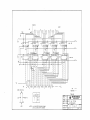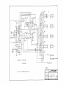
1
User’s Manual
Model DTC-500SP
Cryogenic Temperature
Indicator/Controller
Obsolete Notice:
This manual describes an obsolete Lake Shore product. This manual is a copy from our archives
and may not exactly match your instrument. Lake Shore assumes no responsibilityfor this manual
matching your exact hardware revision or operational procedures. Lake Shore is not responsible
for any repairs made to the instrument based on information from this manual.
Lake Shore Cryotronics, Inc.
575 McCorkle Blvd.
Westerville, Ohio 43082-8888USA
Internet Addresses:
[email protected]
[email protected]
Visit Our Website:
www.lakeshore.com
Fax: (614)891-1392
Telephone: (614)891-2243
Methods and apparatus disclosed and described herein have been developed solely on company funds of Lake Shore Cryotronics, Inc.
No government or other contractual support or relationship whatsoever has existed which in any way affects or mitigates proprietary
rights of Lake Shore Cryotronics, Inc. in these developments. Methods and apparatus disclosed herein may be subject to U S . Patents
existing or applied for. Lake Shore Cryotronics, Inc. reserves the right to add, improve, modify, or withdraw functions, design
modifications, or products at any time without notice. Lake Shore shall not be liable for errors contained herein or for incidental or
consequentialdamages in connection with furnishing, performance. or use of this material.
Obsolete Manual
1980
Table of Contents
Section
I.
General Information
1.1 I n t r o d u c t i o n
1 . 2 D e s c r i p t i o n and A p p l i c a t i o n s
1.3 General S p e c i f i c a t i o n s
1 . 4 Major Assemblies Supplied
1.5 Accessory Equipment and Custom Options Available
II.
III.
IV.
Installation
2 . 1 Introduction
2.2 I n i t i a l I n s p e c t i o n
2 . 3 Power Requirements
2.4 Grounding Requirements
2.5 I n s t a l l a t i o n
2.6 Repackaging f o r Shipment
Operation I n s t r u c t i o n s
3.1 I n t r o d u c t i o n
3.2 Controls, I n d i c a t o r s , and Connectors
3.3 I n i t i a l Checks
3.4 Temperature Readout Mode
3.5 Constant Temperature Control Mode
3.6 Manual Reset Heating Mode
3.7 Temperature Readout Mode (Sensor B)
3.8 Current Source M o d i f i c a t i o n
3 . 9 Remote Temperature Programming
3.9.1 Remote Voltage Programming
3.9.2 Remote R e s i s t a n c e D i v i d e r Programming
3.9.3 Remote P a r a l l e l BCD Input/Output Option
3.10 Grounding
Theory o f Operation
4.1 I n t r o d u c t i o n
4.2 General D e s c r i p t i o n
4.3 Detailed Description
a. Power S u p p l i e s
b. Diode Constant Current Supply
c . S e t Point Voltage
d . Input Internal-Remote C i r c u i t r y
e. Summing V a r i a b l e Gain Amplifier
f . Null Meter C i r c u i t
g. Automatic Reset C i r c u i t , Bounding C i r c u i t
h. Automatic Rate Circuit
i. Output Power A m p l i f i e r
k . Heater Current Metering and Limiting
Page
1
1
1
3
3
5
5
5
5
5
6
8
8
10
10
14
17
17
17
17
17
18
20
20
23
23
24
24
24
24
24
25
25
26
27
27
28
i
Sect ion
V.
VI.
Maintenance and Trouble Shooting
5.1 I n t r o d u c t i o n
5.2 T e s t Equipment and Accessories
5.3 General Remarks
5.4 S e r v i c i n g P r i n t e d C i r c u i t Boards
5.5 Operational Checks
5.6 C a l i b r a t i o n ofSensor Current
5.7 Zero Offset of Input Buffer Amplifier
5.8 Zero Offset of Summing Amplifier
5.9 Adjustment o f t h e D i g i t a l Set Point
Page
34
34
34
35
35
36
36
37
37
Appendices
ii
Table of Illustrations
Model DTC-500SP Cryogenic Temperature
Indicator/Controller
V
Figure 2.1
Sensor and Heater Cables
7
Table 3.1
Entry Number Correlation
8, 9, 10
Figure 3.1
Front Panel
11
Figure 3.2
Rear Panel
12
Figure 3.3
Block Diagram, DTC-500SP Temperature Controller
13
Figure 3.4
Temperature versus Time Characteristics of
Controller
16
Figure 3.5
Remote Temperature Programming
18
Figure 3.6
Programming Networks
18
Figure 3.7
Programming Voltage
19
Table 3.2
Parallel BCD Input of Set Point
21
Table 3.3
Parallel BCD Output of Sensor Voltage
22
Table 4.1
Translation of Null Error versus Set-Point
Deviation
26
Internal/Remote Circuitry Indicating Switching
and Summing of Input Signals
29
Simplified Equivalent Circuit and Transfer
Function of Gain Summing Amplifier
30
Simplified Equivalent Circuit of Automatic
Reset Amplifier
31
Simplified Equivalent Circuit of Automatic
Rate Amplifier
32
Circuit Schematic for Power Stage Showing
Switching of Full Scale Current
33
Figure 5.1
Circuit Schematic Diagram
38
Figure 5.2
Parts Layout for Printed Circuit Board
39
Figure 5.3a, b
Circuit Schematic Diagram for BCD In/Out Option
40
Figure 5.4
Circuit Board Component Diagram for BCD In/Out
Option
41
Parts List for DTC-500SP
42
Figure 1.1
Figure 4.1
Figure 4.2
Figure 4.3
Figure 4.4
Figure 4.5
Table 5.1
iii
SECTION I
General Information
1.1
Introduction
This section contains a description of the Model DTC-500SP Cryogenic
Temperature Controller, its applications, general specifications, major
assemblies supplied and accessory equipment available.
1.2 Description and Applications
The Model DTC-500SP Cryogenic Temperature Controller is housed in an
aluminum case with standard 19" relay panel front for rack mounting. All
connections are at the rear o f the case with all normal operating controls on
the front panel. The instrument is line operated from either 115 volt or 230
volt mains, 50 o r 60 Hertz.
The controller is designed to accept a voltage signal from a temperature
sensitive transducer (generally a DT-500 o r TG-100 Series Diode which is
not supplied), compare this signal with an internal set point voltage,
amplify and process their difference (error signal), and drive an external
heating element. An internal precision 10 microampere constant current source
is provided to excite the temperature transducer.
The error processing section of the controller is of the proportional plus
integral and differential mode design, Generous amplifier gain ranges have been
provided to affect rapid closed loop response times, low steady state temperature
offsets and to insure system stability over a wide range o f thermal system
parameters.
The output power-amplifieris capable of supplying up to 25 watts of heater
power. In view of the high cost of some cryogenic fluids such as helium, cost
consciousness suggests that cryostat design and operating strategies be planned
to limit heater power requirements to substantially less than forty watts.
The principal intended application of the DTC-500SP Controller is as a
constant temperature regulator for laboratory size cryostats. Its basic design,
however, enables it to be used as a general purpose controller for sensors whose
outputs range between 0 and 3.0 volts and whose incremental sensitivities are
in the range of tenths of millivolts o r greater.
In addition to its use as a closed loop automatic temperature controller,
the Model DTC-500SP Controller may be used as a precision thermometer. By
adjusting the set point voltage so that the error signal (as indicated by the
null meter) is zero, the output voltage of the temperature sensor is accurately
obtained. Reference to a voltage versus temperature calibration curve for the
transducer in use will then give its temperature.
1.3 General Specifications
The following specifications for the DTC-500SP Controller are applicable
when used with the TG-100 or DT-500 full range temperature sensitive diodes.
1
General :
Controller Range
0.0001 volt to 2.9999 volts
1 K to 400 K for DT-500 series diodes
Heater Output
25 watts maximum
Sensor
Models DT-500 or TG-100, temperature
sensitive diodes, single-ended or
floating models
Sensor Input
Four terminal connection, constant
current, potentiometric
Sensor Current
10 microamperes
Input Line Voltage
115V o r 230V, 50-60 Hz
Power Consumption
65 watts
Circuit Design
Solid State
Weight
8.2kg (18 lbs.)
Dimensions
5¼" high, 19" wide, 11½ deep, rack
mounting
Sensitivity
~4 Amp/millivolt into 40
at maximum setting
resistor
Temperature Control:
Set Points
Internal, 0 to 3.0 volts via 5 digital
thumbwheels. Remote, Analog - 0 to
-3.0 volts; Digital - (optional)
parallel BCD
Control Accuracy
±0.0005 K, 1 to 28 K
Setpoint Repeatability
±100 microvolts
Control Modes
Proportional (gain), integral reset and
derivative rate
Manual Control
0 to 100% of full output
Automatic Reset
1 to 100 second variable time constant,
or off
Rate
1 to 100 second variable time constant,
or off
in a properly
±0.005 K, 28 t o 400 K { designed system for
DT-500 series diodes
2
Manual Output Control Range
Potentiometer control, 0 to full
scale of current setting
Full Scale Heater Current
Ranges
10mA, 30mA, 100mA, 300mA, 1A
Heater Resistance
25
Maximum Power Output
Ranges
4 x 10 -3 to 40 watts
Controller Proportional Gain
4 Amp/mV in automatic mode (nominal)
for maximum power
in multiples of 10
Temperature Readout:
(Two sensor connections, front panel selectable between control sensor and
temperature sensing only sensor)
Accuracy
100 microvolts calibration error of
sensor and calibration error of full
scale set point
Excitation Current
10 microamperes
Excitation Current Regulation
0.02%
Sensor Calibration Chart
Must be supplied by manufacturer of
sensor in use.
±0.02%
1.4 Major Assemblies Supplied
The Model DTC-500SP Cryogenic Temperature Controller includes as standard
equipment, in addition to the controller proper, the following additional
components:
A.
1
- Operating and Service Manual
B.
2
- Five pin plugs for temperature sensor cables
C.
1
- Seven pin plug for remote set point cable
Temperature sensitive diodes are not supplied as part of the DTC-500SP
Controller.
1.5 Accessory Equipment and Custom Options Available
The following accessory equipment and custom options are available from
the factory. Items marked with an asterisk (*) are of a custom nature. The
customer should discuss these items with a factory representative before
ordering.
A.
Extra 5 and 7 pin connectors
3
B. Multisensor selector panel.
(Special low thermal offset switch
and cabling for selecting among multiple sensors.)*
C.
Custom modification of sensor current supply value.*
D. DT-500 Silicon Temperature Sensitive Diode o r TG-100 Gallium
Arsenide (uncalibrated). (See data sheets at end o f this manual for
nominal operating characteristics and case styles available).
E.
DT-500 Silicon Temperature Senstive Diode o r TG-100 Gallium Arsenide
(calibrated). Standards laboratory calibration service for correlating
diode output voltage withdiode temperature. See sensor data sheet
for additional information. Also see Cryogenic Calibration Service
data sheet.
F.
Power boosters for heater power requirements in excess of forty watts,
o r other than forty ohm heater resistance.
G.
BCD Input/Output (Optional). Include parallel BCD input of set point
and a parallel BCD output of sensor voltage.
4
SECTION II
Installation
2.1
Introduction
T h i s s e c t i o n c o n t a i n s i n f o r m a t i o n and i n s t r u c t i o n s n e c e s s a r y f o r t h e
i n s t a l l a t i o n and s h i p p i n g - o f t h e Model DTC-500SP Cryogenic Temperature Cont r o l l e r . Included a r e i n i t i a l i n s p e c t i o n i n s t r u c t i o n s , power and grounding
r e q u i r e m e n t s , i n s t a l l a t i o n information and i n s t r u c t i o n s f o r repackaging f o r
shipment.
2.2
I n i t i a l Inspection
T h i s i n s t r u m e n t was e l e c t r i c a l l y and mechanically i n s p e c t e d p r i o r t o
shipment. I t should be f r e e from mechanical damages, and i n p e r f e c t working
o r d e r upon r e c e i p t . To confirm t h i s , t h e i n s t r u m e n t s h o u l d be i n s p e c t e d v i s u a l l y f o r obvious damage upon r e c e i p t and t e s t e d e l e c t r i c a l l y by u s e t o d e t e c t any
concealed damage. Be s u r e t o i n v e n t o r y a l l components s u p p l i e d b e f o r e d i s c a r d i n g any s h i p p i n g m a t e r i a l s .
If t h e r e i s damage t o t h e i n s t r u m e n t i n t r a n s i t ,
be s u r e t o f i l e a p p r o p r i a t e claims w i t h t h e carrier, a n d / o r i n s u r a n c e company.
P l e a s e a d v i s e t h e company o f such f i l i n g s . I n case o f p a r t s s h o r t a g e s , p l e a s e
a d v i s e t h e company. The s t a n d a r d Lake Shore C r y o t r o n i c s warranty i s given on
page ii.
2.3
Power Requirements
Before c o n n e c t i n g t h e power c a b l e t o t h e l i n e , a s c e r t a i n t h a t t h e l i n e v o l t age s e l e c t o r s w i t c h (115V o r 230V) i s i n t h e a p p r o p r i a t e p o s i t i o n f o r t h e l i n e
v o l t a g e t o be used. Examine t h e power l i n e f u s e , FU1, (Key No. 14, Page 12)
t o i n s u r e that it i s a p p r o p r i a t e f o r t h e l i n e v o l t a g e .
(115V = 0.75 Amp, 230V
= 0.40 Amp). Nominal p e r m i s s i b l e l i n e v o l t a g e f l u c t u a t i o n i s ±10% a t 50 t o 60 Hz.
CAUTION:
2.4
Disconnect l i n e c o r d b e f o r e i n s p e c t i n g o r changing l i n e f u s e .
Grounding Requirements
To p r o t e c t o p e r a t i n g p e r s o n n e l , t h e National Electrical Manufacturers'
A s s o c i a t i o n (NEMA) recommends and some l o c a l codes r e q u i r e instrument p a n e l s
and c a b i n e t s t o be grounded. This instrument i s equipped w i t h a three-conductor
power c a b l e , which, when plugged i n t o an a p p r o p r i a t e r e c e p t a c l e , grounds t h e
instrument.
2.5
Installation
The DTC-500SP C o n t r o l l e r i s a l l s o l i d s t a t e and d o e s n o t g e n e r a t e s i g n i f i c a n t h e a t except i n t h e 1 amp s c a l e . I t may t h e r e f o r e be r a c k mounted i n c l o s e
proximity t o o t h e r equipment i n dead a i r spaces. However, t h e h e a t from such
a d j a c e n t equipment should not s u b j e c t t h e DTC-500SP C o n t r o l l e r t o an ambient
temperature i n excess of 50 C (122°F). A s w i t h any p r e c i s i o n instrument, i t
should not be s u b j e c t e d t o t h e shock and v i b r a t i o n s which u s u a l l y accompany
high vacuum pumping systems.
5
The recommended c a b l e diagrams f o r t h e s e n s o r diode and h e a t e r element
are given i n F i g u r e 2 . 1 (a) and ( b ) . The u s e of a f o u r w i r e diode c o n n e c t i o n
i s h i g h l y recommended t o avoid i n t r o d u c i n g l e a d I R drops i n t h e v o l t a g e s e n s i n g
p a i r which i s t r a n s l a t e d i n t o a t e m p e r a t u r e measurement e r r o r . The i n d i c a t e d
s h i e l d i n g c o n n e c t i o n s a r e t h e recommended s t a n d a r d p r a c t i c e t o a v o i d ground
loops. The a l t e r n a t e w i r i n g scheme shown i n Fig. 2:1 (c) may be used f o r t h e
diode, i n less c r i t i c a l a p p l i c a t i o n s where c o n t r o l i s i m p o r t a n t , b u t small
t e m p e r a t u r e r e a d o u t e r r o r s can be t o l e r a t e d .
The h e a t i n g element should b e f l o a t e d t o p r e c l u d e t h e p o s s i b i l i t y o f any
of t h e h e a t e r c u r r e n t being conducted i n t o t h e diode s e n s o r l e a d s . E l e c t r i c a l
feedback i n a d d i t i o n t o t h e d e s i r e d t h e r m a l feedback, may cause o s c i l l a t i o n s
and c e r t a i n l y erroneous t e m p e r a t u r e r e a d i n g s .
I n s p e c t t h e h e a t e r element f u s e FU2, (Key No. 16, Pg. 12) f o r p r o p e r value.
( 3 AG, 1.0A, F a s t Blow, o r smaller c u r r e n t r a t i n g i f d e s i r e d . ) This f u s e prot e c t s t h e o u t p u t a m p l i f i e r from damage i n case o f h e a t e r element s h o r t i n g .
Use of a l a r g e r f u s e may cause damage t o t h e instrument and i n v a l i d a t e s t h e
instrument warranty.
2.6
Repackaging f o r Shipment
Before r e t u r n i n g an i n s t r u m e n t t o t h e f a c t o r y f o r r e p a i r , p l e a s e d i s c u s s
t h e malfunction w i t h a f a c t o r y r e p r e s e n t a t i v e . He may be a b l e t o suggest seve r a l f i e l d t e s t s which w i l l p r e c l u d e r e t u r n i n g a s a t i s f a c t o r y instrument t o t h e
f a c t o r y when t h e malfunction i s e l s e w h e r e . If it i s i n d i c a t e d t h a t t h e f a u l t
i s i n t h e i n s t r u m e n t a f t e r t h e s e t e s t s , t h e r e p r e s e n t a t i v e w i l l send s h i p p i n g
i n s t r u c t i o n s and l a b e l s f o r r e t u r n i n g i t .
When r e t u r n i n g an i n s t r u m e n t , p l e a s e a t t a c h a t a g s e c u r e l y t o t h e i n s t r u ment i t s e l f (not on t h e s h i p p i n g c a r t o n ) c l e a r l y s t a t i n g :
A.
Owner and address
B.
Instrument Model and S e r i a l Number
C.
Malfunction symptoms
D.
D e s c r i p t i o n of e x t e r n a l c o n n e c t i o n s and c r y o s t a t s .
If t h e o r i g i n a l c a r t o n i s a v a i l a b l e , repack t h e i n s t r u m e n t i n p l a s t i c bag,
p l a c e i n c a r t o n u s i n g o r i g i n a l s p a c e r s t o p r o t e c t p r o t r u d i n g c o n t r o l s , and
c l o s e c a r t o n . Seal l i d w i t h p a p e r o r nylon t a p e . A f f i x m a i l i n g l a b e l s and
"FRAGILE" warnings.
If t h e o r i g i n a l c a r t o n i s n o t a v a i l a b l e , wrap t h e i n s t r u m e n t i n p r o t e c t i v e p l a s t i c wrapping m a t e r i a l b e f o r e p l a c i n g i n an i n n e r c o n t a i n e r . P l a c e
shock absorbing m a t e r i a l around a l l s i d e s o f t h e instrument t o p r e v e n t damage
t o p r o t r u d i n g c o n t r o l s . P l a c e t h e i n n e r c o n t a i n e r i n a second heavy c a r t o n
and s e a l w i t h t a p e . Affix m a i l i n g l a b e l s and "FRAGILE" warnings.
6
FIGURE 2 . 1
SENSOR AND HEATER CABLES
7
SECTION III
Operating Instructions
3.1 Introduction
This section contains a description of the operating controls, their adjustment under normal operating conditions, typical controller applications and
suggested cryostat adjustment techniques. These instructions are predicated
upon the instrument having been installed as outlined in Section II. The diode
polarity as shown in Fig. 2.1(a) in particular must be correct. A calibrated
diode is assumed to be connected, as shown in Fig. 2.1(a), to the "Sensor A"
receptacle and a 25 ohm heating element is assumed to be connected to the "Heater"
terminals as shown in Fig. 2.1(b).
3.2 Controls, Indicators and Connectors
The operating controls, indicators and connectors on the instrument's front
and rear panels are shown in Fig. 3.1 and 3.2. The numbers with leaders to
various controls in the figures are keyed to the entries in Table 3.1.
Table 3.1
- Entry Number Correlation
1
SET POINT - VOLTS
0 - 2.9999
Digital set point of sensor voltage
2
GAIN
Gain Multiplier, X1, X10, X100
3
GAIN
Variable gain 1-10. Together with gain
multiplier, allows adjustment of overall
controller gain over 1000 to 1 range
4
MAN. B , MAN. A,
AUTO A
Mode selector switch: AUTO A uses sensor
A to automatically control temperature.
MAN. A disengages automatic control feature
but permits readout of sensor A voltage.
MAN. B permits readout of sensor B voltage.
5
MAN. RESET
When mode selector switch (4) is in either
MAN. B position, the MAN. RESET
potentiometer permits the user to manually
adjust the current to the heater element.
(Caution: High current settings will quickly
boil away cryogenic fluids).
MAN. A or
6
AUTO-RESET
OFF, MIN. - MAX.
Adjusts auto-reset time constant of integrator.
(See Fig. 3.3) Effectively determines times
constant of integrator between 100 and 1
seconds, "MIN." and "MAX." respectively, or
"OFF".
8
7
Adjusts A u t o - r a t e time c o n s t a n t o f d i f f e r e n t i a t o r . E f f e c t i v e l y determines time
c o n s t a n t o f d i f f e r e n t i a t o r between 1 and 100
seconds, "MIN." and "MAX." r e s p e c t i v e l y , o r
"OFF".
RATE
OFF, MIN.-MAX.
A. C . l i n e s w i t c h (ON/OFF) and p i l o t l i g h t .
8
POWER
9
F.S. CURRENT
-
AMPS
Switch s e l e c t e d c u r r e n t s e l e c t o r . Use of a
low s e t t i n g w i l l avoid i n a d v e r t e n t b o i l - o f f
i n s e t t i n g up system, and/or system o s c i l l a t i o n s .
10
HEATER CURRENT
Monitors h e a t e r element c u r r e n t . F u l l s c a l e
d e f l e c t i o n c o r r e s p o n d s t o MAX. HEATER - AMP.
s w i t c h (9) s e t t i n g ,
11
NULL
I n d i c a t e s t h e d i f f e r e n c e between t h e s e t p o i n t
v o l t a g e and t h e s e n s o r o u t p u t v o l t a g e . Meter
i s n o n - l i n e a r f o r l a r g e e r r o r s o f e i t h e r sign.
See page 23 and 24 f o r d i s c u s s i o n .
12
INT.
13
115-230 VAC
A. C. l i n e v o l t a g e s e l e c t o r s l i d e switch
(50-60 Hz).
14
0.75-0.4 AMP.
A. C. l i n e f u s e (FU1). See p a r a . 2.3.
115 VAC-0.75 AMP., 230 VAC - 0.4 AMP.
15
NO LABEL
A. C. l i n e cord
16
1.0A, F.B.
Heater element l i n e f u s e , 1 AMP., Fast Blow
17
SENSOR A, J1
(Five p i n ,
Sensor A c a b l e r e c e p t a c l e .
Amphenol t y p e 126-217 Plug)
18
SENSOR B, J2
Sensor B c a b l e r e c e p t a c l e . (Five p i n ,
Amphenol t y p e 126-217 Plug) J2
19
REMOTE INPUT, J 3
Remote s e t p o i n t e i t h e r by means o f 0 t o -3
(Amphenol
v o l t signal o r a p o t e n t i o m e t e r .
126-195 P l u g ) . 53
20
J4
40 p i n connector f o r "REMOTE"
option
21
HEATER
Heater element l e a d t e r m i n a l s (Grey i s t h e
high s i d e and Black i s t h e low s i d e ) .
-
REM.
S e l e c t s between i n t e r n a l set p o i n t and remote
set p o i n t . The center p o s i t i o n a l l o w s a
mixture of b o t h set p o i n t s . Front panel s e t
p o i n t i n o p e r a t i v e w i t h switch i n "REMOTE"
position.
BCD i n / o u t
9
Name
Function
22
GROUND
Chassis ground terminal
23
NO LABEL
Heat s i n k f o r output t r a n s i s t o r s
No. Key
3.3 I n i t i a l Checks
I n i t i a l checks, c a l i b r a t i o n checks, and s e r v i c i n g procedures are d e s c r i b e d
i n S e c t i o n V, MAINTENANCE.
3.4 Temperature Readout Mode
To u s e t h e DTC-500SP as a c r y o g e n i c thermometer t o measure t h e t e m p e r a t u r e
of a c a l i b r a t e d diode connected t o SENSOR A t e r m i n a l s , i n i t i a l l y p o s i t i o n
s w i t c h e s and c o n t r o l s as f o l l o w s :
A.
Temperature set p o i n t s w i t c h (Key No. 12) t o i n t e r n a l , "INT.".
B.
Mode switch (Key No. 4) to "MAN. A".
C.
"MAN.
D.
F.S.
E.
"GAIN"
F.
"RESET"
G.
"RATE"
H.
"POWER" switch (Key NO. 8 ) t o on.
RESET" (Key N o . 5) t o zero.
CURRENT
- AMPS"
(Key No. 9) t o 0.01.
(Key No. 2 and 3) t o minimum s e t t i n g .
(Key No. 6) t o o f f .
(Key No. 7) t o o f f .
The n u l l meter w i l l probably d e f l e c t o f f s c a l e ( e i t h e r l e f t o r r i g h t ) when t h e
power s w i t c h is turned on. I f t h e d e f l e c t i o n is t o t h e r i g h t , t h e set p o i n t v o l t a g e
i s less t h a n t h e sensor v o l t a g e . I f t h e d e f l e c t i o n is t o t h e l e f t , the set p o i n t
v o l t a g e is g r e a t e r t h a n t h e s e n s o r v o l t a g e . I n o t h e r words, i n o r d e r t o n u l l t h e
meter, t u r n t h e set p o i n t i n t h e d i r e c t i o n t h a t you wish t h e n e e d l e t o move.
I f t h e n u l l meter w i l l n o t n u l l r e g a r d l e s s of t h e set p o i n t v o l t a g e check t o
make s u r e t h a t t h e p r i n t e d c i r c u i t cord l o c a t e d behind t h e thumbwheel d i g i t s h a s
n o t worked l o o s e from i t s p r o p e r p o s i t i o n d u r i n g shipping. This can b e e a s i l y
observed by removal of t h e t o p cover.
A d j u s t t h e set p o i n t v o l t a g e u n t i l t h e "NULL" meter is c e n t e r e d w h i l e i n c r e a s i n g
t h e "GAIN" toward maximum. I n c r e a s i n g t h e v o l t a g e w i l l move t h e meter p o i n t e r t o
t h e l e f t ; decreasing t h e set p o i n t v o l t a g e w i l l d e f l e c t t h e meter p o i n t e r t o t h e
r i g h t . A f t e r c e n t e r i n g t h e meter, t h e s e t p o i n t v o l t a g e can b e read d i r e c t l y t o
100 µ v o l t s . A t a b l e of r e l a t i v e s e n s i t i v i t y f o r t h e n u l l meter as a f u n c t i o n of
g a i n s e t t i n g is given on page 24.
A f t e r determining t h e s e t p o i n t v o l t a g e , r e f e r t o t h e d i o d e c a l i b r a t i o n c h a r t
t o a s c e r t a i n t h e diode t e m p e r a t u r e .
10
11.
12.
13
3.5 Constant Temperature Control Mode
Assume t h a t a c a l i b r a t e d diode i s i n u s e as d e s c r i b e d i n paragraph 3 . 4 . To
m a i n t a i n a constant temperature, determine t h e corresponding s e t p o i n t v o l t a g e
from t h e diode c a l i b r a t i o n c h a r t . S e t t h i s v o l t a g e on t h e "SET POINT" s w i t c h e s .
P o s i t i o n c o n t r o l s - a s i n d i c a t e d below:
A.
Temperature s e t p o i n t switch (Key No. 1 2 ) t o "INTERNAL".
B.
Mode switch (Key No. 4 ) t o "AUTO A.".
C.
''MAN.
D.
"F.S. CURRENT - AMPS" (Key No. 9) t o 1 . 0 AMP.
E.
"GAIN"
F.
"RESET" (Key No. 6) t o o f f .
G.
"RATE" (Key No. 7) t o o f f .
H.
"SET POINT-VOLTS" s w i t c h (Key No. 1 ) t o v o l t a g e corresponding t o d e s i r e d
temperature.
I.
"POWER" switch (Key No. 8) t o on.
RESET" (Key No. 5) t o zero.
(Keys No. 2 and 3) t o minimum s e t t i n g s .
If t h e block o r sample h o l d e r whose t e m p e r a t u r e i s t o be c o n t r o l l e d i s c o l d e r
t h a n t h e s e t p o i n t temperature, t h e s e n s o r d i o d e v o l t a g e w i l l be high and t h e n u l l
meter w i l l d e f l e c t t o t h e r i g h t : Slowly i n c r e a s e t h e "GAIN" s e t t i n g (Keys No. 2
and 3). The "HEATER CURRENT" meter should show an immediate up s c a l e d e f l e c t i o n
p r o p o r t i o n a l t o t h e "GAIN" s e t t i n g . The "NULL" meter should s t a r t t o come o f f i t s
f u l l r i g h t d e f l e c t i o n p o s i t i o n as t h e g a i n i s i n c r e a s e d . A s t h e sample h o l d e r
t e m p e r a t u r e approaches t h e set p o i n t temperature, t h e NULL meter w i l l approach
c e n t e r s c a l e and t h e "HEATER CURRENT" meter w i l l assume a s t e a d y v a l u e even w i t h a
f u r t h e r i n c r e a s e i n t h e g a i n s e t t i n g . Continue t o i n c r e a s e t h e gain u n t i l a n
i n c r e m e n t a l change i n g a i n produces a n e g l i g i b l e r e d u c t i o n i n t h e n u l l e r r o r , b u t
n o t s o high as t o produce o s c i l l a t i o n s .
To f u r t h e r reduce t h e n u l l e r r o r , r o t a t e t h e "AUTO RESET" gain c o n t r o l (Key No.
6 ) o u t o f t h e d e t e n t ( o f f ) p o s i t i o n i n t h e clockwise d i r e c t i o n . A s t h e c o n t r o l
i s advanced, t h e n u l l meter should approach t h e c e n t e r p o s i t i o n with unobservable
e r r o r . Leave t h e "AUTO RESET" v e r n i e r i n t h e p o s i t i o n r e q u i r e d t o reduce t h e n u l l
e r r o r t o zero, but below any l e v e l which induces o s c i l l a t i o n s .
A f t e r achieving a s t a b l e o p e r a t i n g p o i n t , reduce t h e "F.S. CURRENT - AMPS"
(Key No. 9) t o a lower s e t t i n g . A s lower s e t t i n g s are d i a l e d i n t h e p e r c e n t (%)
o f maximum, h e a t e r c u r r e n t being used should i n c r e a s e . The optimum a r e a f o r
c o n t r o l can be obtained by keeping t h e meter p o i n t e r between 0.2 and 0 . 7 on t h e
meter f a c e .
14
Abruptly i n c r e a s e t h e set p o i n t v o l t a g e by t e n m i l l i v o l t s . The s e n s o r
v o l t a g e now r e p r e s e n t s a temperature warmer than t h a t r e p r e s e n t e d by t h e s e t p o i n t
v o l t a g e . The NULL meter should d e f l e c t t o t h e l e f t and t h e HEATER CURRENT should
go t o zero immediately. A s t h e sample h o l d e r c o o l s , t h e NULL METER p o i n t e r should
r e t u r n toward zero.
A s t h e NULL METER p o i n t e r approaches z e r o , t h e HEATER CURRENT w i l l i n c r e a s e
from zero t o t h e new s t e a d y s t a t e v a l u e r e q u i r e d t o maintain t h e sample a t t h e
lower temperature r e q u e s t e d . The NULL METER should read z e r o as t h e HEATER CURRENT
s t a b i l i z e s a t i t s new v a l u e .
Now a b r u p t l y decrease t h e s e t p o i n t v e r n i e r c o n t r o l by t e n m i l l i v o l t s . The
sensor v o l t a g e now r e p r e s e n t s a temperature c o l d e r than t h a t r e p r e s e n t e d by t h e
s e t p o i n t v o l t a g e . The NULL meter should d e f l e c t t o t h e r i g h t and t h e HEATER
CURRENT meter should d e f l e c t toward f u l l s c a l e . A s t h e sample h o l d e r h e a t s ,
t h e NULL meter p o i n t e r w i l l t e n d t o zero and t h e HEATER CURRENT meter r e a d i n g w i l l
d e c r e a s e toward i t s new s t e a d y s t a t e v a l u e . A s t h e NULL meter c e n t e r s , t h e
HEATER CURRENT should s t a b i l i z e a t t h e new c o n s t a n t value r e q u i r e d t o maintain
t h e d e s i r e d temperature.
A s k e t c h of t h e temperature v e r s u s time p a t t e r n d e s c r i b e d above i s given i n
Figure 3 . 4 . Observe t h a t t h e r e i s no temperature overshoot o r o s c i l l a t i o n when
(This statement
t h e "GAIN" and "AUTO RESET" c o n t r o l s a r e p r o p e r l y a d j u s t e d .
presupposes t h a t t h e sample h o l d e r , h e a t e r , and sensor may be a c c u r a t e l y modeled
as a simple R-C t y p e time c o n s t a n t thermal c i r c u i t . )
If o s c i l l a t i o n o r overshoot are observed when changing t h e set p o i n t v o l t a g e
i n small increments, reduce t h e G A I N and i n c r e a s e t h e AUTO RESET time c o n s t a n t
( r o t a t e CCW) s e t t i n g s u n t i l o s c i l l a t i o n s a r e no longer observed and/or a d j u s t
t h e "F.S. CURRENT - AMPS" (Key No. 9) t o a lower s e t t i n g .
Normally a t cryogenic t e m p e r a t u r e s , t h e above adjustments w i l l r e s u l t i n a
s t a b l e system with good t r a n s i e n t response due t o t h e s h o r t t i m e c o n s t a n t s
encountered a t t h e s e temperatures. For t h e s e c o n s t a n t s , t h e r a t e s w i t c h should
I f , however, t h e t r a n s i e n t response o f t h e system
remain i n an o f f p o s i t i o n .
must be improved, t h i s can b e done by t h e a d d i t i o n of r a t e ( o r d e r i v a t i v e ) t o
the control functions.
Physically, t h e
system. The system
e r r o r , but a l s o i d s
then t h e c o n t r o l l e r
of t h e system.
e f f e c t can be d e s c r i b e d as i n t r o d u c i n g a n t i c i p a t i o n i n t o t h e
r e a c t s n o t o n l y t o t h e magnitude and i n t e g r a l (RESET) o f t h e
probable v a l u e i n t h e f u t u r e . If t h e e r r o r i s changing r a p i d l y ,
responds f a s t e r . The n e t r e s u l t is t o speed up t h e response
To i n c r e a s e system response ( i f needed) t a k e t h e "RATE" c o n t r o l (Key No. 7 )
out o f t h e d e t e n t (off) p o s i t i o n i n t h e clockwise d i r e c t i o n . F o r v a r i o u s s e t t i n g s
of t h e c o n t r o l , observe t h e t r a n s i e n t response t o a change i n s e t p o i n t . Too
short a timeconstant may r e s u l t i n o s c i l l a t i o n and an u n s t a b l e system, A change in
gain may be necessary t o e l i m i n a t e o s c i l l a t i o n o r overshoot.
15
FIGURE 3.4
TEMPERATURE VERSUS TIME
CHARACTERISTICS OF CONTROLLER
16
3.6 Manual Reset Heating Mode
By p l a c i n g t h e mode s e l e c t o r s w i t c h (Key No. 4) i n e i t h e r p o s i t i o n MAN. A o r
MAN. B, a manually s e t t a b l e c o n s t a n t c u r r e n t may be supplied t o t h e h e a t e r element.
The magnitude o f t h e c u r r e n t i s determined by t h e s e t t i n g of t h e MAN RESET
potentiometer (Key No. 5) and t h e F.S. CURRENT - AMPS switch (Key No. 9 ) . The
c u r r e n t supplied t o t h e h e a t e r i s i n d i c a t e d on t h e HEATER CURRENT meter. The
f u l l s c a l e reading o f t h e meter corresponds t o t h e F . S . CURRENT - AMPS switch
s e t t i n g . MAN RESET a l l o w s t h e u s e r t o hold a temperature f o r a s h o r t p e r i o d o f
time i n an open hoop c o n d i t i o n while h e u s e s t h e n u l l meter and t h e d i g i t a l s e t
p o i n t t o read a second s e n s o r . This i s accomplished by a d j u s t i n g t h e output
c u r r e n t (Key No. 5) such t h a t t h e h e a t e r c u r r e n t (Key No. 10) does n o t v a r y when
switched from Auto A toMAN. A o r MAN. B (Key No. 4 ) .
3.7 Temperature Readout Mode (Sensor B)
I n some a p p l i c a t i o n s , t h e temperature i s c o n t r o l l e d (or r e g u l a t e d ) a t one
p h y s i c a l l o c a t i o n w h i l e it i s d e s i r e d t o measure t h e temperature a t a second
l o c a t i o n . This r e q u i r e s two s e n s o r s , "Sensor A" l o c a t e d a t t h e t e m p e r a t u r e c o n t r o l
p o i n t and "Sensor B" a t t h e second p o i n t where only t h e temperature i s t o be
measured. Sensor B must be c a l i b r a t e d .
3.8 Current Source M o d i f i c a t i o n
The c u r r e n t s o u r c e w i t h i n t h e DTC-500SP i s f l o a t i n g and p r e s e n t l y e x c i t e s
e i t h e r Sensor A o r Sensor B, depending on t h e switch p o s i t i o n o f t h e mode s e l e c t o r
s w i t c h (Key No. 4 ) . A simple w i r i n g change can be made s o t h a t b o t h Sensors A and
B are e x c i t e d s i m u l t a n e o u s l y i f e i t h e r o r both s e n s o r s a r e e l e c t r i c a l l y i s o l a t e d
from a common ground. With t h e instrument l i d removed, u n s o l d e r t h e wire t o Pin A,
Sensor B connector, and r e s o l d e r t o Pin A, Sensor A c o n n e c t o r a n d r e s o l d e r t o Pin B,
Sensor B connector (now two w i r e s on t h i s t e r m i n a l ) . Now s o l d e r a wire between
Pin B, Sensor A connector, and Pin A, Sensor B connector. The two s e n s o r s a r e now
connected i n s e r i e s . If you wish t o u s e o n l y Sensor A, make up a s h o r t i n g plug f o r
Sensor B terminal t h a t s h o r t s Pin A t o P i n B.
For some a p p l i c a t i o n s , a c o n s t a n t c u r r e n t o t h e r than 10 µA i s d e s i r e d . This
c o n s t a n t c u r r e n t i s programmed by means o f t h e following formula: I ~ 4.99/R7 with
R5 b e i n g a t r i m f o r t h i s c u r r e n t . For 10 µA, R7 i s 499K; f o r 100 µA, R7 must be
49.9K. The c u r r e n t s o u r c e can be programmed between 1 µA and 1 mA, i f d e s i r e d . The
compliance v o l t a g e i s s l i g h t l y l e s s t h a n 5 v o l t s .
3.9 Remote Temperature Programming
Three types o f remote programming a r e a c c e p t a b l e by t h e DTC-500SP.
They a r e :
A. An analog signal from 0 t o -3 v o l t s (standard)
B. An e x t e r n a l r e s i s t a n c e d i v i d e r ( s t a n d a r d )
C. A p a r a l l e l BCD s e t p o i n t i n c l u d i n g an A/D c o n v e r t e r w i t h p a r a l l e l BCD
of t h e s e n s o r v o l t a g e ( o p t i o n ) .
Remote temperature c o n t r o l can be achieved by applying e i t h e r A o r B of t h e above.
signals and switching t h e "SET POINT" t o t h e "REMOTE" p o s i t i o n o r t h e c e n t e r "MIX"
p o s i t i o n . In t h e "MIX" p o s i t i o n , t h e remote signal a n d - t h e i n t e r n a l set p o i n t
a r e added d i r e c t l y .
3 . 9 . 1 Remote Voltage Programming
To apply a remote v o l t a g e s i g n a l t o t h e DTC-500SP, connect a 0 t o -3 v o l t
s i g n a l between ( t h e analog ground) E and Pin A .
17
3.9-2. Remote Resistance Divider Programming
Remote temperature control can also be achieved by connecting an external
resistance divider to 53 and switching the "SET POINT" to the ''REMOTE"position
or the center "MIX" position. Pin D of J3 is a precision regulator of 6.9 volts
+5%. To insure maximum accuracy, the total resistance between pins E-D of 53
should be greater than 10,000 ohms. Since the signal desired is less than 3 volts,
a dropping resistor, Rd, must be used to limit the voltage across the variable
resistor to less than 3 volts. The remote set point diagram is shown in Figure 3.5.
Figure 3.5-Remote Temperature Programming
A number o f external temperature programming networks are shown in Figure 3.6.
Figure 3.6-Programing Networks
18
The following is a suggested procedure for designing external temperature set
point control circuitry:
A.
Determine the range of desired temperature control voltage.
B. Choosethe most suitable control circuit for your application:
- 100%
a)
Temperature control range
b)
Limited temperature control range
c)
Fixed temperature set points selected in steps
d)
Most flexible arrangement allowing for selected steps
and continuously variable temperature set points.
Additional variations o f the above may be tailored to fit the
intended application.
C. To insure that the total resistance between pins E & D of the external
programming voltage divider be o f the correct value to develop a drop
of 3 volts across the programming resistor, it is suggested that the
divider calculation be based on more than 1600 ohms per 1 volt and a
shunting resistor (RT in Fig. 3.6) used for precision trimming to 3
volts.
The 3.0 volts can be measured with a precision floating voltmeter,
with the sensor circuit open, i.e., sensor plugs disconnected, o r
calibrated with the DTC-500SP internal set point volts switch as
follows :
a)
Connect a precision known resistor R (any value between 50K-250K)
to the pins AE and BD of the Sensor A input plug J1 (Amphenol type
126-217 or equivalent) in place of the sensor as shown in Fig. 3.7,
and turn the sensor selector switch on the front panel to Manual A
position.
A
Figure 3.7-Programming Voltage, J1
The voltage drop across resistor R is equal to 10 x 10-6 (amperes) x
R (ohms) volts, thus a 100 K ohm resistance would result in a 1 volt
drop. With the "TEMPERATURE SET POINT" switch in "INTERNAL" position,
the null meter will indicate zero error when the internal temperature
set point switch on the front panel is at 1.000 volts. Increase the
19
gain to maximum and adjust the internal set point, if necessary, for
the null meter to indicate zero. Move the reference set point switch
to "EXTERNAL" position and adjust trim resistor RT on the external
set point programming instrument so that the null meter reads zero.
The external programming network is now matched to the internal
reference source. Although one point calibration as described
above is sufficient, it may be desirable to check several points.
In that case, a precision rheostat may be used for R at the sensor
input connector. However, the leads as well as the divider resistor
should be shielded, and the shields connected to pin H of the sensor
A input connector (J1). Similarly, the leads and box housing the
externally programmable temperature resistance network should be
shielded through pin H of external set point plug (J3).
3.9.3 Remote Parallel BCD Input/Output Option
The remote programming option consists of a TTL parallel 18-bit
set point voltage and a TTL parallel 17-bit output of one-half of the
sensor voltage. It is assumed that the sensor voltage output can be
multiplied by two within the computer. The cable pin-out connectors are
indicated in Tables 3.2 and 3.3.
Both the internal and external BCD input of the set point is
accomplished either in the "INTERNAL"or "MIX" position by setting connector
J4 pin-38 high (+5V) for external BCD or low (0 V) for internal BCD
Both
internal and external BCD set points are disabled in the "REMOTE"position.
Note that in the "MIX" position either BCD set point can be combined with an
external signal from connector J1.
.
The BCD output of one-half of the sensor voltage is present in all
modes, "INTERNAL","MIX", and "REMOTE".
3.10 Grounding
The chassis is grounded by the 3 lead power cable to the electrical
supply common ground. The common lead of the controller circuitry ("Lo"
terminal ofthe heater output - Key 21, Fig. 3.2) can be externally connected
to the chassis ground terminal. Although the grounding of the controller
common is normal operation practice, the common "Lo" terminal may be disconnected from chassis ground if doing so helps to eliminate accidental ground
loops within the system.
-
The effect of grounding may be observed by mounting the a.c. signal
present on the heater circuit. Choose the connection which reduces the a.c.
signal to its lower value.
20
Table 3 . 2
PARALLEL BCD INPUT OF SET POINT
Function
Pin
-
Pin
Function
2
BCD .0008
54 - 2 2
BCD .04
54 - 4
BCD .0002
54 - 24
BCD .01
6
BCD .0004
5 4 - 26
BCD .8
54 - 8
BCD .0001
5 4 - 28
BCD .2
5 4 - 10
BCD .008
5 4 - 30
BCD .4
54
-
12
BCD .002
5 4 - 32
BCD .1
54
-
14
BCD .004
54
-
34
BCD 2
5 4 - 16
BCD .001
5 4 - 36
BCD 1
BCD .08
5 4 - 38
I f high (+5V)
54
54
54
-
-
18
Select Remote
Set Point
5 4 - 20
BCD .02
5 4 - 40
21
Table 3.3
PARALLEL BCD OUTPUT OF SENSOR VOLTAGE
Function
Pin
Pin
Function
54
-
1
BCD .0001
54
-
21
BCD .04
54
-
3
BCD .0002
54
-
23
BCD .08
54
-
5
BCD .0004
54
-
25
BCD .1
54
-
7
BCD .0008
54
-
27
BCD .2
54
-
9
BCD .001
54
29
BCD .4
54
-
11
BCD .002
54
-
31
BCD .8
54
-
13
BCD .004
54
-
33
BCD 1.
54
-
15
BCD .008
54
-
35
54
-
17
BCD .01
54
-
37
54
-
19
BCD .02
54
-
39
Note:
Common Ground
BCD output is one-half of actual sensor voltage.
22
SECTION IV
Theory of Operation
4.1
Introduction
This section contains the theory o f operation of the DTC-500SP Controller
and a functional characterization of the controller in Laplace transform notation
to aid the thermal system designer in system stability analysis.
In some applications, it may be required for an experienced user to modify
the gain, reset or rate range. The information given within this section should
make these modifications straightforward.
4.2
General Description
Refer to Figure 3 . 3 and Figure 5.1 as an aid in the following discussion.
A precision constant current source causes 10 microamperes of DC current to bias
the control diode. The voltage developed across the control diode is fed through
a buffer amplifier and this voltage generates a positive current through the
3 megohm resistor into the current summing amplifier.
The digital set point is converted to an analog voltage by the five digit
The resulting voltage is negative and an appropriate resistance
string is chosen so that its current into the summing amplifier just balances
the sensor generated positive current. The result is zero current at the summing
junction when the set point voltage is just equal to the sensor voltage.
D/A converter.
Because a current summing operational amplifier is used, many signals can
be mixed together, Therefore, the digital set point signal can be mixed with the
remote signals described in Section 3 . 9 . The gain of the controller is built
into this summing operational amplifier. A simplified equivalent Circuit of this
amplifier is shown in Figure 4.2 The associated switching from sensor A to
sensor B and the switching associated with the internal and remote switch are
shown in Figure 4.1. From Figure 4.1, it can be seen that the error signal i s
a current which is amplified as a voltage by the variable gain operational
amplifier U10 of Figure 4.2. The amplified error is displayed on the NULL meter
and also applied through an inverter to (1) an integrator circuit (reset), (2)
a bound or clamping circuit and (3) a differentiator circuit (rate),
The error signal, its integral and differential, are summed as current by
the operational amplifier U12. This amplifier then drives the output power
circuit. The current from the power amplifier is metered by the current meter.
Changing the current range from 10mA to 1 Amp changes the voltage gain of the
output stage from 0.2 to 20. Closed loop control action is achieved through
the thermal path between the heater element and the temperature sensing diode.
23
Detailed Description
4.3
(a)
Power S u p p l i e s
There a r e f o u r r e g u l a t e d s u p p l y v o l t a g e s w i t h i n t h e DTC-500SP.
They are d e s i g n a t e d as P/S-1 through P/S-4 (Figure 5 . 1 ) . P/S-1,
c o n s i s t i n g o f a d i o d e b r i d g e and r e g u l a t o r U18, s u p p l i e s a r e g u l a t e d
15 v o l t s and an u n r e g u l a t e d 18 v o l t s t o t h e Lake Shore C r y o t r o n i c s
c o n s t a n t c u r r e n t s o u r c e . P/S-2 and P/S-3 c o n s i s t o f a d i o d e b r i d g e
w i t h r e g u l a t o r s U16 and U17 which supply +15 v o l t s and -15 v o l t s
r e s p e c t i v e l y . P/S-4, c o n s i s t i n g o f a diode b r i d g e and r e g u l a t o r U15,
s u p p l i e s t h e +5 v o l t s u s e d for t h e o p t i o n only.
P/S-5 i s an u n r e g u l a t e d supply f o r t h e o u t p u t power s t a g e . The
output v o l t a g e i s 25 v o l t s on t h e one ampere s c a l e and approximately
7.5 v o l t s for a l l lower c u r r e n t s e t t i n g s .
(b)
Diode Constant Current Supply
Power s u p p l y P/S-1 and o p e r a t i o n a l a m p l i f i e r A1 c o n s t i t u t e t h e
main components i n t h e d i o d e c o n s t a n t c u r r e n t s u p p l y . Due t o t h e
h i g h i n p u t impedance o f t h e o p e r a t i o n a l a m p l i f i e r A1, t h e d i o d e c u r r e n t
i s f o r c e d t o flow through r e s i s t o r R 5 developing 4.99V at 10 microamperes.
The v o l t a g e a c r o s s R5 i s t h e r e f o r e equal t o t h e v o l t a g e a t t h e i n v e r t i n g
i n p u t (-) t e r m i n a l o f A 1 w i t h a v o l t a g e o f 4.99V a p p l i e d t o t h e noni n v e r t i n g (+) i n p u t o f A1 by t h e r e f e r e n c e c i r c u i t o f R 1 , R 2 , R 3 , R4
a n d CRS. The c u r r e n t through R5 (4.99 K) w i l l maintain t h e r e g u l a t e d
c u r r e n t t h r o u g h s e n s o r t o 10 microamperes.
The e n t i r e c o n s t a n t c u r r e n t supply system was d e s i g n e d t o be
f u l l y f l o a t i n g s o t h a t t h e cathode o f t h e s e n s o r d i o d e might be
r e t u r n e d t o common.
(c)
S e t P o i n t Voltage
The d i g i t a l set p o i n t c o n s i s t o f a d i g i t a l - t o - a n a l o g c o n v e r t e r
which is l i n e a r t o approximately 1ppm. I t s a c c u r a c y i s o b t a i n e d by a
simple, symmetrical a p p l i c a t i o n o f t h e mark: s p a c e r a t i o p r i n c i p l e .
A s i n g l e up/down c o u n t e r chain i s u s e d , which a l t e r n a t e l y c o u n t s down
-
t o zero and up t o t h e maximum from t h e v a l u e t o be c o n v e r t e d . The
first of t h e s e i n t e r v a l s i s used f o r t h e 'mark' t i m e , t h e second f o r
t h e ' s p a c e ' t i m e ; t h e sum o f t h e two b e i n g independent o f t h e i n p u t
value. This c i r c u i t has a r e s p o n s e t i m e o f approximately one second
and i s advantageous f o r s e t t i n g up s t e a d y s t a t e v o l t a g e s where a f a s t
response t o changes i n i n p u t i s n o t r e q u i r e d . The c i r c u i t i s described
i n d e t a i l i n a p a p e r by J . R. Stockton*.
(d)
Input Internal-Remote C i r c u i t r y
Figure 4 . 1 shows p a r t o f t h e i n p u t c i r c u i t r y f o r t h e DTC-500SP.
*
"A simple, h i g h l y l i n e a r mark:space r a t i o d i g i t a l - t o - a n a l o g
c o n v e r t e r . " J . R . Stockton, J . o f Physics E : S c i e n t i f i c
Instruments, 1977, Vol. 1 0
24
The s e n s o r select s w i t c h s e l e c t s e i t h e r sensor A o r s e n s o r B v o l t a g e
l e a d s as i n d i c a t e d as w e l l as s w i t c h i n g t h e c u r r e n t l e a d s (not shown).
Note t h a t t h e n e g a t i v e v o l t a g e l e a d i s grounded w i t h t h e c u r r e n t source
n e g a t i v e and p o s i t i v e l e a d s f l o a t i n g . The s e n s o r v o l t a g e goes through
a b u f f e r a m p l i f i e r p r i o r t o b e i n g converted t o a p o s i t i v e s i g n a l
c u r r e n t by r e s i s t o r R15. T h i s b u f f e r e d v o l t a g e i s a v a i l a b l e t o t h e
u s e r a t t e r m i n a l B o f J3. R 1 3 (110 ohms) i s p r e s e n t so t h a t
i n a d v e r t a n t s h o r t i n g o f t h i s o u t p u t does n o t d e s t r o y t h e b u f f e r
amplifier.
The INT-REM s w i t c h s e l e c t s between t h e i n t e r n a l s e t p o i n t and
t h e external set p o i n t s . I n i t s c e n t e r p o s i t i o n , t h e i n t e r n a l s e t
p o i n t and t h e remote s e t p o i n t s i g n a l s ( i f p r e s e n t ) a r e mixed. Do
n o t use t h e mix p o s i t i o n u n l e s s you i n t e n d t o u s e both i n t e r n a l and
remote s i g n a l s , s i n c e t h e remote s e t p o i n t w i l l t e n d t o g e n e r a t e
In t h e remote p o s i t i o n , t h e unused
n o i s e i f no s i g n a l i s p r e s e n t .
i n p u t should be grounded s o as t o e l i m i n a t e p o t e n t i a l s o u r c e s o f
noise.
Note t h a t a l l e x t e r n a l s i g n a l s must be n e g a t i v e as well as t h e
i n t e r n a l set p o i n t . A t n u l l , t h e c u r r e n t from t h e s e n s o r i s j u s t
balanced by t h e n e g a t i v e c u r r e n t ( s ) from i t s s e t p o i n t ( s ) r e s u l t i n g
i n e r r o r signal which i s dependent on t h e gain s e t t i n g f o r no r e s e t
and zero f o r t h e normal o p e r a t i o n when r e s e t i s engaged.
(e)
Summing V a r i a b l e Gain Amplifier
A s i m p l i f i e d u n i t f o r t h e summing a m p l i f i e r i s shown i n Figure
4 . 2 . Capacitors C14 and C15 are p r e s e n t f o r h i g h frequency s t a b i l i t y .
Since a l l i n p u t c u r r e n t s flow through equal r e s i s t o r s , an e q u i v a l e n t
e r r o r v o l t a g e s i g n a l i s Ve = ie R15, w i t h Rg e i t h e r , 10K, o r 1 K .
The gain o f t h i s a m p l i f i e r v a r i e s from 2 t o 2000 depending on t h e
p o s i t i o n of t h e v a r i a b l e g a i n p o t e n t i m e t e r and g a i n m u l t i p l i e r s w i t c h .
Not shown i n F i g u r e 4 . 2 are t h e n u l l r e s i s t o r s R19, R26, R28 and
t h e t r i m r e s i s t o r R27. The trimming o f t h i s a m p l i f i e r i s d e s c r i b e d i n
Section 5.8. CR3 and CR4 are 6 . 8 v o l t zener d i o d e s which a r e p r e s e n t
t o keep t h e a m p l i f i e r o u t o f s a t u r a t i o n due t o extraneous n o i s e s p i k e s .
(f)
Null Meter C i r c u i t
D i r e c t l y a f t e r t h e v a r i a b l e g a i n summing a m p l i f i e r i s t h e n u l l
meter c i r c u i t . The Null Meter i s d e s e n s i t i z e d f o r l a r g e e r r o r s by
p l a c i n g two germanium d i o d e s a c r o s s i t s t e r m i n a l s . The r e s u l t i s a
l i n e a r s c a l e f o r e r r o r l e s s t h a n 50% o f f u l l d e f l e c t i o n i n e i t h e r
d i r e c t i o n with high n o n - l i n e a r i t y f o r l a r g e r e r r o r s . Sensor-set
p o i n t e r r o r i n n u l l can be r e l a t e d t o gain s e t t i n g s by t h e following
t a b l e f o r small e r r o r s :
25
Table 4.1
Translation of Null error versus set-point deviation as a function
of gain :
Gain
1
5
10
50
100
500
1000
(g)
Sensor Set-Point Error, mV/div.
70
36
7
3.1
.75
.35
.08
Automatic Reset Circuit, Bounding Circuit
The bound circuit and variable gain integrator shown in Figure 5.3
are realized by operational amplifiers U11 and U13 respectively. A
simplified equivalent circuit of the circuit is given in Figure 4.3.
Note, from Figure 5.1, that the amplified error signal (Vo) is
inverted (Amplifier U11) prior to being integrated by this amplifier.
Application of the principle that the summing junction currents must
add to zero yields the overall transfer function of the stage.
The bounding circuit disables the integrating function for large
errors when rapid corrective action is desired, The memory action of
integrating Capacitor C19 causes the controller to be sluggish in such
transient operations. The method of disabling the capacitor depends
upon the sign of the error and the polarity of the voltage across C19.
When the sensor voltage (Vs)is smaller than the set point voltage
(Vsp), the error signal VE = Vs - VsP<o and an over-temperature condition
exists. The input voltage (-Vo) to the reset amplifier is also negative
resulting in an output voltage which would integrate towards a large
positive value. To avoid this condition, since reset is not required,
the diode CR6 essentially shorts the output to ground.
If, however, the sensor voltage is larger than the set point voltage
(Vsp), the error signal is positive and an under-temperature condition
exists. If the input voltage (-VO) = |Av1|Ve<2 volts, then the output
voltage of the comparator (U11) is -15 volts. The integrator is therefore
disabled since the diode CR5 is contrasting with its anode close to -14 volts.
For an input signal (-Vo)between zero and two volts, the integrator
is operational and ultimately, once the system is controlling and stable,
the voltage developed across C19 becomes just equal to the error voltage
(Vo) which is required to hold a constant temperature under open loop
conditions. Since this voltage is now present on the capacitor of the
reset amplifier, it is no longer needed at the output of the gain
summing amplifier resulting in the error signal reducing to zero,
26
The switch is closed when the AUTO RESET control is in the off
position and the amplifier gain is approximately 10-3.
(h)
Automatic Rate Circuit
For most cryogenic applications, the addition of rate will not
greatly enhance the system response. However, in some applications,
rate will improve response. The simplified circuit and transfer
function are shown in Figure 4.4. Note that an output is only
present for a rapidly changing input signal, and that the time
constant varies from 1.85 to 187 seconds.
With the AUTO RATE switch closed, the circuit is effectively
disabled from the controller since the gain is less than 10-3.
(i)
Output Power Amplifier
The output power stage consists of a summing amplifier and
two stages of voltage amplification, an output switching network
and a variable supply voltage.
First note that on the one ampere scale the supply voltage is
25 volts while on all other maximum current ranges the supply voltage
is approximately 7.5 v o l t s .
Since VI = E +/edt + de/dt for R39 = R55 = R56 = 20K, the voltage
gain associated with the summing amplifier U12 is -R58/20K = -5.
Writing a mode equation at VE1 yields:
-5v1
VI
R59
e
(IB1+ IB2
20K
-
Vo
+
0.6 )
R63
+
Vo
-
(-5VI)
R61
~
VI
20K
+
VO +
5VI
9K
-20
VI
Therefore, on the 1 ampere scale, the voltage gain is -20 and the
voltage drop across R69 is 0.5 volts so that 40 volts is available
across the load resistor if the input signal is -2 volts.
The voltage gain of the power stage is reduced for all other
current settings. For example, on the 10mA scale, the voltage gain
is (-20) (I40)/13 = ( - 8 ) / 1 3
-0.6 where I = 10mA. The input signal
for full scale is therefore I40(-0.6) = -0.24 volts.
(j)
Manual Heater Control
When the mode selector switch is set to either MAN A o r MAN B
position, switch section S1F connects the input of the power amplifier
stage to the wiper of potentiometer R57 through resistor R74. Varying
the wiper position from zero to its maximum will vary the output voltage
at the collector of Q2 from 0 to 25 volts on the 1 ampere scale and
from 0 to 7.5volts for all other current selectors. The heater element
current is thus varied proportionally to the setting of R57 and the
maximum heater current switch (54) position.
27
(k)
Heater Current Metering and Limiting
The heater element current is measured by the heater current
ammeter, shunted by resistor R65 through R69 as appropriate for the
current range selected. The full scale output current is determined
by the series combination of the heater element resistance and one
of the group of resistors R70 through R73. This series combination
is connected across the nominal7.5 or 25 volt output of the power
amplifier. Approximately .5 volts appears across the Heater Current
Meter (M1)and R200 and its appropriate shunt resistor.
Under no circumstances shall the rating of fuse FU2 be increased
above one ampere in an attempt to achieve a power dissipation of 25
watts in a heater element whose resistance is less than 25 ohms.
Such a substitution invalidates the instrument warranty and is
likely to damage the output power amplifier circuit.
28
FIGURE 4.1
Internal/Remote Circuitry Indicating Switching and
Summing of Input Signals
29
Figure 4.2
S i m p l i f i e d E q u i v a l e n t C i r c u i t and T r a n s f e r
F u n c t i o n of G a i n Summing A m p l i f i e r
30
Figure 4.3
Simplified Equivalent Circuit of Automatic Reset Amplifier
31
Figure 4.4
Simplified Equivalent Circuit of Automatic Rate Amplifier
32
33
SECTION V
Maintenance and Troubleshooting
5.1 Introduction
This section contains instructions for maintaining and calibrating the
controller, nominal voltage values and gains, circuit schematic diagram,
printed circuit board component diagram and parts list.
5.2 Test Equipment and Accessories
An RCA Senior Voltohmyst vacuum tube voltmeter o r an equivalent high
input impedance digital voltmeter; a 25 ohm, 25 watt resistor to simulate
the heater element; and a precision resistor connected to simulate the diode in
a connector assembly wired according to Fig. 2.1 (c) are normally sufficient for
testing and calibrating the DTC-500SP Controller.
5.3 General Remarks
Upon initial installation, the single most probable cause of system malfunction is an improperly connected temperature sensing diode. If it is impossible to zero the null meter at any setting of the set point voltage controls,
carefully examine the cable/diode assembly to insure that the diode polarity is
correct, that the sensor is plugged into the "SENSOR A" receptacle and that the
"TEMPERATURE SET POINT" switch is in the INTERNAL position.
Because o f the highly reliable solid state design of the controller, it is
most unlikely that the controller will be a source o f difficulty. For this
reason, it is advisable to examine other portions of the cryogenic system before
testing the controller proper. Some suggested checks are:
A.
Open or shorted sensor and heater leads, particularly in the vicinity
of the sample holder if it is subject to frequent dis-assembly.
B.
Leakage paths between heater and sensor leads giving rise to electrical feedback in addition to thermal feedback.
C. Premature l o s s of cryogenic fluid due to thermal shorts in dewar, ice
blocks in lines, sample holder immersed in cryogen, sample holder
in vapor whose temperature i s above the controller set point temperature,
etc.
D. Excessive thermal path phase lags will cause the control loop to be
unstable at high gain settings. Physical separation between the diode
and heater, particularly by paths of small thermal cross-section should
be avoided.
E. Examine heater element fuse FU2.
If it is indicated that the controller is malfunctioning after performing
the tests to be described below, it is recommended that the instrument be returned
to the factory for repair. The components used in the instrument are costly and
may be permanently damaged if subjected to inappropriate test voltages o r excessive
soldering iron heat. Although premium materials and techniques have been used to
34
fabricate the instrument circuit board, there is always the risk of lifting
a connection pad o r cracking the board when unsoldering a component.
5.4 Servicing Printed Circuit Boards
It i s suggested that components be unsoldered for trouble shooting only
as a last resort since ample information is available at the numbered terminal
pins. Attempt to infer component currents by voltage tests rather than removing
a lead and seriesing it with an ammeter. All voltages are available for measurement from the top side of the printed circuit board. When it is necessary to
replace a component, access is available by removing the bottom cover.
Use a low heat (25 to 50 watts) small-tip, freshly tinned soldering iron.
Use small diameter, rosin core solder. Remove a component lead by applying heat
to the lead, observing the solder melt and then pulling the lead through the board
from the top side. Never apply tension to printed wiring from the bottom side.
Thoroughly clean all of the old solder from the mounting hole before inserting a new component with the use of a wick or desoldering suction device. Shape
the new component and insert in mounting hole. Do not use heat o r force to
insert the new component. If the leads will not go through the hole, file the
lead o r clean the hole more thoroughly. Once mounted properly, apply heat to
lead and wiring pad simultaneously and resolder. Clean excess flux from the
connection and adjoining area with warm water and weak detergent if need be.
(Contamination i n some areas of the board can seriously degrade the high input
impedance of the operational amplifiers.)
5.5
Operational Checks
Replace the sensor diode connector plug with a test plug made up according
to Fig. 2.1 (c). Substitute a precision resistor for the sensor diode in the
test plug. Remove the heater element leads and place a forty watt, forty ohm
resistor across the heater output terminals.
Ten microamperes flowing through the test resistor should develop a potential
of 1.00 volts across a 100 K ohm resistor. With the gain set a maximum position
and the mode selector switch in position MAN. A (assuming the test plug is in
SENSOR A receptacle), attempt to null the error with a set point voltage in the
vicinity of 1.0 volts. The null meter should swing smoothly as the set point
voltage is varied in the vicinity of the null.
While still in the MAN. A position, set the MAXIMUM HEATER AMP switch at
1 amp. Vary the MAN. RESET potentiometer from zero toward its maximum. The
current meter should increase linearly along with the advance of the MAN. RESET
control. With the MAN. RESET control set to give mid-scale heater current meter
deflection, rotate the MAX. HEATER AMP switch through all of its positions. The
heater current meter indication should remain approxmately at mid-scale in all of
the positions.
Zero the null meter with the set point voltage controls. Turn the AUTO
RESET and GAIN controls to mid-scale position. Set the MAX. HEATER CUR. switch
to 1 amp. Position the mode control switch to AUTO A. Abruptly change the set
35
point voltage sufficiently to cause a +10 unit deflection of the NULL meter to the
right. The heater current meter deflection will consist of two components. The
first is a rapid step rise due to the steady null error and a second, gradually
rising component due to the AUTO RESET circuit integrating the steady error.
The heater current meter will gradually rise toward full scale deflection. The
rate at which the heater current rises is determined by the AUTO RESET time constant
setting. The rate is a minimum in the counterclockwise position and a maximum
in the fully clockwise position.
Abruptly change the set point voltage to cause -10 units deflection of the
NULL meter to the left. The HEATER CURRENT meter should gradually decrease from
full scale deflection to zero. The rate at which the current meter goes to zero
is in part determined by the bounding circuit. Its non-linear behavior accounts
for the assymetryin the temperature versus time characteristics as shown in
Figure 3 . 4 .
If the instrument responds to the tests outlined above as indicated, either the
trouble lies elsewhere in the system or the malfunction in the controller is of
a subtle nature. As an aid in trouble shooting in the latter case, typical voltages
and gains under specified conditions are given in Section 5.10.
5.6
Calibration of Sensor Current
The sensor current has been factory calibrated to 10 microamperes ±10
nanoamperes. To check the sensor current without removing the case cover, a
conveniently available precision resistance of not less than .01% tolerance should
be connected to pins A-B of the sensor connector socket (J1 or J 2 ) , and the
sensor selector switch on the front panel switched to the appropriate sensor
input (A o r B). The "TEMPERATURE SET POINT" switch should be switched to "REMOTE",
and remote plug (53) be disconnected.
A high quality potentiometric voltmeter connected to the precision resistor
should measure a voltage equal to 10 microamperes times the value of the resistor.
Typically, a 100 K ±.01% resistor should read 1.0000 within 100 microvolts. If
recalibration is indicated, the voltage across the precision resistors can be
recalibrated after removing the case cover and adjusting trimmer R5 on the
circuit board.
Note that due to the non-linearity of the diode, the adjustment of the
current source does not have to be to thesame level of accuracy as the measurement
of voltage across the sensor.
5.7
Zero Offset of Input Buffer Amplifier
This amplifier has been trimmed at the factory and should not require
immediate attention. After a few months of operation, it may introduce some measurement error due to a zero offset. For example a 1mV zero offset in the output
would correspond to approximately a 0.4 K offset in the sensor reading above 30K
where the sensitivity is approximately 2.5mV/K. Below 25 K where the sensitivity
is approximately 50mV/K, this would result in an appreciably smaller error.
36
T h i s o f f s e t may be zeroed as i n d i c a t e d below:
5.8
A.
Allow 20 minutes f o r w a r m up o f t h e c o n t r o l l e r .
B.
Make a s h o r t i n g p l u g s o t h a t Pins E and D , t h e sensor input v o l t a g e
leads t o t h e b u f f e r a m p l i f i e r a r e shorted. Place t h i s shorting plug
i n J1.
C.
Mode s w i t c h (Key No. 4) t o ''MAN. A".
D.
Use a HIGH i n p u t impedance v o l t m e t e r t o monitor output of b u f f e r
a m p l i f i e r . The ground connection i s Pin D of J1. The output connection
i s p i n 6 o f U9.
E.
Adjust t r i m R10 s o t h a t t h e a m p l i f i e r o f f s e t i s l e s s than ±100µV.
Zero Offset o f Summing A m p l i f i e r
T h i s a m p l i f i e r has also been trimmed a t t h e f a c t o r y and should n o t r e q u i r e
immediate a t t e n t i o n . I n o r d e r t o z e r o t h e o f f s e t o f t h i s a m p l i f i e r , it i s nece s s a r y t o first zero t h e o f f s e t o f t h e i n p u t b u f f e r a m p l i f i e r (Section 5 . 7 ) .
With t h e s h o r t i n g plug i n p l a c e (J1) and no o t h e r i n p u t s t o t h e summing a m p l i f i e r ,
i . e . , no i n p u t s t o J3 o r J4, set t h e d i g i t a l set p o i n t t o 0.0000 v o l t s . Adjust
t h e t r i m potentiometer R27so t h a t t h e n u l l meter (Key No. 11) i s a t zero w i t h
t h e g a i n (Keys No. 2 and 3) a t i t s h i g h e s t v a l u e . Both a m p l i f i e r s a r e now i n
b a l a n c e with zero o f f s e t .
5.9
Adjustment o f t h e D i g i t a l S e t Point
The adjustment o f t h e d i g i t a l s e t p o i n t r e q u i r e s o n l y a p r e c i s i o n r e s i s t o r
i n t h e range from 50 K t o 250 K. Let us assume t h a t t h e r e s i s t o r has t h e v a l u e
100,010 ohms.
A.
Complete s e c t i o n s 5.6-5.8.
B.
Place t h e p r e c i s i o n r e s i s t o r i n p l a c e o f J1 u s i n g t h e connection
diagram shown i n F i g u r e 2 . 1 ( c ) .
C.
S e t t h e d i g i t a l s e t p o i n t (Key No. 1) t o 1.0001 v o l t s .
D.
Adjust t r i m p o t e n t i o m e t e r R25 s o t h a t t h e n u l l meter reads zero w i t h
t h e gain (Keys No. 2 and 3) t o i t s h i g h e s t v a l u e .
The r e - c a l i b r a t i o n o f your c o n t r o l l e r i s now complete.
37
41
5.9 Parts List, Component Location Diagram and Schematic
Table 5.1
PARTS LIST FOR DTC-500SP
R1
R2
R3
R4
R5
R6
R7
R8
R9
R10
R11
R12
R13
R14
R15
R16
R17
R18
R19
R20
R21
R22
R23
R24
R25
R26
R27
R28
R29
R30
R31
R32
R33
R34
R35
R36
R37
R38
R39
R40
¼W
1%
3.92K
8250 ohm
¼W
1%
499 ohm
1/8W
1%
3.75K
1/8W
1%
5K Trim Pot (constant current adjust)
10K
¼W
0.5%
499K
¼W
1%
3.83K
¼W
1%
Not present
100K Trim Pot (Buffer - Zero)
Not present
Not present
1.0K
100K
909K
1M
10K
1M
¼W
¼W
¼W
¼W
¼W
¼W
1%
1%
.1%
.1%
.1%
.1%
Not present
100K
¼W
1%
845K
¼W
1%
423K
¼W
1%
423K
¼W
1%
93.1K
½W
20K Trim Pot (D/A Converter Adjust)
.1%
Not present
100K Trim Pot (Summer - Zero)
Not present
10K Pot (Gain Control)
8.25K
1.96 M
100K
1K
10K
¼W
¼W
¼W
5%
.1%
1%
1/8W
1%
¼W
0.5%
¼W
¼W
1%
1/8W
1%
½W
¼W
1%
.5%
Not present
1.02K
1.0K
3.92K
20K
2.8K
1%
42
R41
R42
R43
R44
R45
R46
R47
R48
R49
R50
R51
R52
R53
R54
R55
R56
R57
R58
R59
R60
R61
R62
R63
R64
R65
R66
R67
R68
R69
R70
R71
R72
R73
R74
R75
R76
R77
R78
R79
R80
c1
c2
c3
c4
c5
C6
2.8K
1K
14.7K
2.0K
10K
¼W
¼W
¼W
¼W
¼W
¼W
1.96 M
1 0 0 K Pot (Reset C o n t r o l )
8.06K
¼W
1.27 M
¼W
1.96 M
¼W
10 M
¼W
.5%
1%
1%
1%
.5%
1%
1%
1%
1%
10%
1%
866 ohm
¼W
1 0 0 K Pot (Rate C o n t r o l )
866 ohm
¼W
1%
200K
¼W
1%
200K
¼W
1%
1 0 K Pot (Manual Reset C o n t r o l )
82.5K
¼W
1%
Not p r e s e n t
Not p r e s e n t
Not p r e s e n t
Not p r e s e n t
Not p r e s e n t
1w
422 ohm
54.9 ohm
1w
16.9 ohm
1w
4.97 ohm
1w
1.64 ohm
1w
.498 ohm
1w
715 ohm
1w
360 ohm
1w
81.6 ohm
1w
62 ohm
¼W
1%
1.5KM
¼W
20%
Not p r e s e n t
150K
¼W
1%
100 ohm
¼W
1%
1470 ohm
¼W
1%
165K
¼W
1%
215 ohm
¼W
1%
.33 MFD, 25V, Mylar
118 PFD, 10V,
Dipped Mylar
Not p r e s e n t
2 . 2 MFD, 35V, Metal Tantalum
Not p r e s e n t
.1 MFD, 100V, Mylar
43
C7
C8
C9
c10
c11
c12
C13
C14
C15
C16
C17
C18
C19
c20
c21
c22
C23
C24
C25
C26
C27
C28
C29
C30
C31
C32
u1
u2
u3
u4
u5
U6
u7
U8
u9
u10
u11
u12
U13
U14
U15
U16
U17
U18
U19
u20
Not present
.27 f, 100V, Electrolytic
.27 MFD, 100V, Electrolytic
.27 MFD, 100V, Electrolytic
.27 f, 100V, Electrolytic
.1 MFD, 100V, Mylar
Not present
.022 MFD, 50V, Mylar
150 PFD, 50V, Dipped Mylar
.047 MFD, 50V, Tantalum
1.0 MFD, 100V, Electrolytic
Not present
1.0 MFD, 100V, Electrolytic
.1 MFD, 100V, Mylar
2600 MFD, 50V, Electrolytic
2700 MFD, 25V, Electrolytic
470 MFD, 25V, Electrolytic
470 MFD, 25V, Electrolytic
470 MFD, 25V, Electrolytic
.1 MFD, 100V, Mylar
.1 MFD, 100V, Mylar
470 MFD, 25V, Electrolytic
50 PFD, 5%
.0015 MFD, 5%
Dipped Mylar
Electrolytic
Presettable up/down Binary Decade Counter
Presettable up/down Binary/Decade Counter
Presettable up/down Binary/Decade Counter
Presettable up/down Binary/Decade Counter
Presettable up/down Binary/Decade Counter
Dual D Edge Triggered Flip-Flop
Quad 2 Input NAND Schmitt Trigger
Dual SPDT Low Resistance Switch
Operational Amplifier
Operational Amplifier
Dual Operational Amplifiers
Operational Amplifier
Operational Amplifier
Operational Amplifier
Positive Voltage Regulator (1.5A)
Negative Voltage Regulator (1.5A)
Positive Voltage Regulator (1.5A)
Positive Voltage Regulator (1.5A)
Operational Amplifier
Voltage Reference
CD4029 AE
CD4029 AE
CD4029 AE
CD4029 AE
CD4029 AE
MC1413 AL
CD4093 BE
AD7512 D1
OP15
OP15
MC 1458P
F741TC
LF356N
LF356N
MC7805
MC7915
MC7815
MC7815
LN308
LM399H
44
3N163
U21
U22
U23
F.E.T.
Not present
Voltage Reference
LM399H
Q1
Power Transistor
2N6044
J1
J2
J3
J4
J5
J6
J7
5 pin sensor socket, Amphenol
5 pin sensor socket, Amphenol
7 pin remote set point, Amphenol
40 pin connector
Heater Binding Post
Heater Binding Post
Chassis Ground Post
F1
F2
Fuse Holder, Littlefuse
Fuse Holder, Littlefuse
CR1
CR2
CR3
CR4
CR5
CR6
CR7
CR8
CR9
CR10
Silicon Diodes
Silicon Diodes
6.2V Zener Diode (Semcor LMZ6.2)
6.2V Zener Diode (Semcor LMZ6.2)
Silicon Diode
Silicon Diode
Silicon Diode Bridge
Silicon Diode Bridge
Silicon Diode Bridge
Silicon Diode Bridge
1N459
WL005
WL005
WL005
W06M
45
Table 5.1
PARTS LIST FOR DTC-500SP
BCD
u1
u2
u3
u4
u5
U6
u7
U8
u9
u10
u11
u12
U13
U14
U15
U16
U17
U18
u19
u20
R101
R102
R103
R104
R105
R106
R107
R108
R109
R110
R112
C101
C102
C103
C104
C105
C106
C107
C108
I/O Option
Level T r a n s l a t o r TTL t o Logic High MOS
Level T r a n s l a t o r TTL t o Logic High MOS
Level T r a n s l a t o r TTL t o Logic High MOS
Level T r a n s l a t o r TTL t o Logic High MOS
Level T r a n s l a t o r TTL t o Logic High MOS
Quad AND -OR S e l e c t Gate
Quad AND-OR S e l e c t GATE
Quad AND-OR S e l e c t Gate
Quad AND-OR S e l e c t G a t e
Quad AND-Or S e l e c t Gate
Quadruple D-Type Flip-Flops
Quadruple D-Type Flip-Flops
Quadruple D-Type Flip-Flops
Quadruple D-Type Flip-Flops
Quadruple D-Type Flip-Flops
Hex B u f f e r s / D r i v e r s w i t h open-collector
High-Voltage Outputs
Hex I n v e r t e r
Quadruple 2-Input P o s i t i v e And Gates
I n t e r f a c e - Analog t o D i g i t a l Converter
I n t e r f a c e - Analog t o D i g i t a l Converter
7.5K
100K
100K
1/8w
1/8w
1/8w
F4104 BPC
F4104 BPC
F4104 BPC
F4104 BPC
F4104 BPC
SIL 4019 BC
SIL 4019 BC
S I L 4019 BC
SIL 4019 BC
SIL 4019 BC
74LS175N
74LS175N
74LS175N
74LS175N
74LS175N
SN7417N
MM 74C14N
74LS08N
I C L 7103 ACPI
ICL 8052 ACPD
1%
1%
1%
1%
1%
300K
¼w
35.7K ¼w
100K
T r i m pot
549
¼w
1%
Not P r e s e n t
Not P r e s en t
14K
¼w
1%
182
1/8w
1%
.1 PF, 100V, Mylar
- 6 8 MFD, 100V, Mylar
1.5 MFD
300 MFD
.22 MFD, 100V, Polypropylene
.68 MFD, 100V, Mylar
Not p r e s e n t
360 MFD
46
C109
C110
C111
C112
C113
.1 MFD,
.1MFD,
.1 MFD,
2.2 MFD,
2.2 MFD,
CR101
CR102
Diodes
Diodes
100V,
100V,
100V,
35V,
35V,
Mylar
Mylar
Mylar
Tantalum
Tantalum
1.5 V
1.5 V
47