1
SECTION I
INTRODUCTION
1.1
GENERi\L DESCRIPTION
The SA455/465 Minifloppy Disk DrlvE!s are enhanced double~headed, half~helght versions of the ShuBarl SAIJOO
minifloppy drives. The SA455/46f> provides up to four Umes the on-line storage capacity, faster access time, nnd
improved reliability and maintainability'.
51\455/465 drives read and write in single and double density on standard 5.25 inch diskettes on both :sides of the
diskettes. The new drives are: half the height of the Shugart SA400 and are plug compatible.
The compact SA455/465 offers a reliable, low cost, high performance alternative to OEM data storage applications where tape cassette units wOUild bave been previously considered.
SA455/465 drives have these standard features: compact size' ~ 1.62 Inches high x 5.75 inches wiele x 7.96
inches deep, and a weight of 3.3 pounds; low heat dissipation; de drive motor with precision servo speed control
(lnd integral tachometer; band positioner; same proprietary glass bonded ferrite/ceramic read/write head as used
in SIIllUml\ Imge floppy drives; Int,ernal write protect circuitry; activity light. and solid die eust chassis.
Typical applications for the SA455/465 are word processing systems, entry level micro-processor systems, intelligent calculators, program storagl:!,hobby computer systems, and other applications where low cost rilndoTl\ access data storage is a requirement.
This manual prOVides depot level maintenance Informatk:m necessary to maintain, trouble-shoot, and repair the
SA455/465. A separate OEM manual (PIN 39238) Is available which describes installation. interface. ,mel power
requirements useful for the applications of the drive.
Key Features
a.
b.
c.
d.
0.5 Mbytes (SA455) or 1.0 Mbyte (SA465) storage capacity (unformatted)
Low power (12.5 wallts)
125/250 kbits/second transfer rate
DC drive motor (eliminates ac requirements)
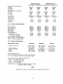
1.2 SPECIFICATION
SUMM~lRY
1.2.1 Perfonnance Specifications
SA455 (40 Track)
Capacity
(in bytes)
Unformatted
Per Disk
Per Surface
Per Track
Single Densit~1 Double Density
(PM)
(MFM)
250,000
125,000
3,125
1·1
500,000
250,000
6,250
SA465 (80 Trad')
Single Denstiy
(FM)
Double Density
(MFM)
500,000
250,000
3,125
1,000,000
500,000
6,250
SA465 (80 Track)
SA455 (40 Track)
Single Density Double Density Single Density Double Density
Formatted (16 Records/Track)
Per Disk
Per Track
Per Sector
Formatted (10 Records/Track)
Per Disk
Per Track
Per Sector
Transfer Rate
Latency (avg.)
Access Time
-rrack to Track
Average
Settling Time
163,840
2,048
128
327,680
4,096
256
327,680
2,048
128
655,360
4,096
256
204,800
2560
256
409,600
5120
512
409,600
2560
256
819,200
5120
512
125 kbits/sec
100 ms
250 kbits/sec
100 ms
125 kblts/sec
100 ms
250 kblts/sec
100 ms
3 ms
94 ms
15 ms
3 ms
94 ms
15 ms
6 ms
93 ms
15 ms
6 ms
93 ms
15 ms
500 ms
300 rpm
2938 bpi
5876 fcl
48 tpi
500 ms
300 rpm
5876 bpi
5876 fci
48 tpi
500 ms
300 rpm
2961 bpi
5922 fcl
96 tpl
500 ms
300 rpm
5922 bpi
5922 fcl
96 tpl
SA154
SA155
SA157
SA154
SA155
SA157
SA164
SA165
SA167
SA164
SA165
SA167
1.2.2 Functional Specifications
Motor Start Til11('
Hotatlotlal Speed
Recording Density
Flux Density
Track Density
Media Requirements
Soft sectored
16 sectors hard sectored
10 sectors hmd sectored
Industry standard flexible diskette
Oxide on O.OO~ in. (0.08 mm) Mylar
5.25 In. (133.4 111m) square jacket
1.2.3 Physical Specifications
Environmental Limits
Ambient Temperature
Relative Humiditv
Maximum Wet Bulb
Shock
Vibration
Operating
Shipping
Storage'
. 50° to 11soF
(10.0° to 46.1°C)
20 to 80%
78°F (25.6°C)
0.5G 10 rns
0.5G 5-600 Hz
-40 0 to 144°F
(.40° to 62. 2°C)
1 to 95%
No Condensation
15G 10 ms
3G 5-600 Hz
_8° to 117°F
(-22.2° to 47.2°C)
1 to 95%
No Condensation
35G 10 ms
3G 5-600 Hz
. DC Voltage Requirements
+·12 V ± 10% @ 1.2 A (max), 0.6 A (typ), 100 mV ripple
+ 5 V ± 5% @ 0.9 A (max:), 0.6 A (typ), 50 mV ripple
Mechanical Dimensions (exclusive of front panel)
Width : 5.75 Inches (146.1 mm)
Height: 1.62 Inches (41.1 mm)
Depth :::::. 7.96 inches (202 mm)
Weight = :t:3Ibs (1.5 kg)
Power Dissipation = 9.6 Watts (34.0 BTU) continuous typical
3.6 Watts (13;.5 BTU) standby
NOTE
Standby: Drive motor off. dr.lve select off, and stepper at reduced current.
1·2
1.2.4
Reliability Specifieatianli
MTBF:
10,000 POH under typical usage.
PM: Not required.
MTTR: :30 minutes.
Error Rates:
Soft Head Errors: 1 per 10" bits Hmd.
I--Iard Head Errors: 1 per 10 1:.1 bits read.
Seel~ Errors: 1 per 10 6 seeks.
Media Lif('.:
Passes per Trac!(: 3.0
Insertions: 30,000 +
j\.3
x 10('
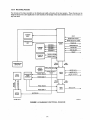
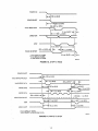
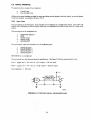
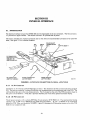
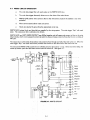
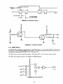
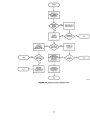
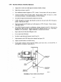
FUNCTIONAL CHARACTERiSTICS
The SA455/465 consists of read/write and control electronics. drive mechanism, read/write head, and precision
track positioning mechanism. These components perform the following functions:
a.
b.
c.
Interpret and generate control signals.
Move read/write heads to the desired track.
Read and write data.
The interface signals and their relationship to the internal functions are shown In figure 1-2.
1.3.1
Read/Write and Control
EIE~ctronics
The electronics package contains:
a,
b.
c,
d.
e.
f.
1.3.2
Index detector circuits
I-lead position actuator driver
Read/write amplifier and liransition detector
Writ e protect detector
Drive select circuit
Drive motor control
Drive Mechanism
The dc drive motor under servo .spE~ed control (using an integral tachometer) rotates the spindle at 300 rpm
through a direct drive system. An expandable collet/spindllB assembly provides precision media positioning to ensure data interchange.
1.3.3
Positioning Mechanics
The read/write head assembly is accul'atelypositioned through the use of a band positioner which is attached to the
head carriage assembly. Precise track location is accomplished as this positioner is rotated in discrete increments by
a stepping motor.
1.3.4 Read/Write Heads
The proprietary heads are a single element ceramic read/write head with tunnel erase elements to provide erased
areas between data tracks. Thus normal interchange tolerances between media and drives will not degrade the
signal·to-noise ratio and diskette interchangeability is ensur,ed.
The read/ write heads are mounted on a carriage which is located on precision carriage ways. The diskette is held
in a plane perpendicular to the read/write heads by a platen located on the base casting. This precise registration
assures perfect compliance with the re,ad/write heads. The read/write heads are in direct contact with the diskette.
The h(~ad surface has been designed to obtain maximum signal transfer to and from the magnetic surface of the
diskette with minimum head/diskette wear.
1·3
1.3.5 Recording Formats
The formats of the data recorded on the diskette are totally a function of the host system. These formats can be
designed around the user's application to take maximum advantage of the total available bits that can be written on
anyone track.
ACTIVITV
LIGHT
1-1-'-,-------.-----1
STEP
DIRECTION SELECT
INDEx/SECTOR
I.ED
1-1-'-.-...- -----,------1
STepPER
MOTOR
-
TRACK 00
SWITCH·
INOEx/SECTOR
MOTOR ON
...
.J
~~
........
0%
:E8
READY
-
TRACK 00 (N/C) _
SIDE
SELECT
-'--1..
•
.
WRITE
WRll'E PROTECT (N/2)
PROTECT
SWITCH
!-+w'RITE PROTECT
....- - - - - '
(COM)
WRITE HEAD 0
WRITE DATA
--
WRITE
LOGIC
WRITE GATE
.
WRITE PROTECT
-
WRITE HEAD l'
SIDE
SELECT
ffi
tu
If
~
o:t
READ HEAD 0
~
....
......
MOTOR
DRIVER
SIDE SELECT
1-t-1'RACK 00 (COM)
It
DRIVE
MOTOR
TRACK 00
STEPPER B
STEPPER C
STEPPER 0
DRIVE
SELECT
REAO/WRITE
HEAD
ASSEMBL''(
DRIVE SELECT (4 LINES)
STEPPER A
INDEx/SECTOR
DETECTOR
I
...
CONTROL
LOGIC
•_ _
R_EA_D_H_EA_D_1·_ _,
.,_ _- - t.......
READ
LOGIC
READ DATA
MC)TOR ON
.......- -----
39238·02·/\
'SA465 ONLY.
FIGURE 1·2. SA455/465 FUNCTIONAL DIAGRAM
1·4
1.4 FUNCTIONAL OPERATIONS
1.4.1 Power Sequencing
Applying dc power to the SA455/465 can be done in any sequence. However, during power up, the WRITE
GATE line must be held inactive or at 4;\ high level. This wlll prevent possible "glitching" of the media. After application of dc power, a 100 ms delay should be introduced bE!fore any operation is performed. After powering on,
Initial position of the read/write heads with respect to the data tracks on the media is indetermlnant. In order to
assure proper positioning of the read/write heads after power on, a Step Out operation should be performed until
the TRACK 00 line becomes active (Recalibrate).
1.4.2 Drive Selection
Drive selection occurs when the propel:' DRIVE SELECT line is activated. Only the drive with this line jumpered
will respond to Input lines or gate output lines.
1.4.3 Motor On
In order for the host system to read or write data, the dc drive motor must be turned on. This is accomplished by
activating the line -MOTOR ON. A 500 ms delay must be introduced after activating this line to allow the motor to
come up to speed before reading or writing can be accomplished.
The motor must be turned off by the hoslt system by deactivating the MOTOR ON line, The control electronics
keep the motor active for 3 seconds, aliter MOTOR ON is deactivated. This allows reselectlng during copy operations and will ensure maximum motor and media life.
1.4.4 Track Accessing
Seeking the read/write heads from one track to another is accomplished by:
a.
Activating the DRIVE SELECT line.
b.
Selecting desired direction IUslng the DIRECTION SELECT line.
c.
WRiTE GATE being inalctive.
d.
Pulsing the STEP line.
Multiple track accessing is accomplished by repeated pulsing of the STEP line (with direction valid) until the desired
track has been reached. Each pulse on the STEP line will cause the read/write heads to move one track either in or
out depending on the DIRECTION SELECT line. Head movement is initiated on the trailing edge of the step
pulse.
1.4.5 Step Out
With the DIRECTION SELECT line at a plus logic level (2.4 to 5.25 V), a pulse on the STEP line will cause the
read/write heads to move one track away from the center of the disk. The pulse(s) applied to the STEP line must
have the timing characteristics shown in 'figures 1-3 and 1-4.
1.4.6 Step In
With the DIRECTION SELECT line at minus logic level (0 to 0.4 V), a pulse on the STEP line will cause the.
read/write heads to move one track <:loser to the center of the disk. The pulse(s) applied to the STEP line must
have the timing characteristics shown in figures 1-3 and 1-4.
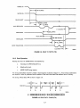
1.4.7 Side Selection
Head selection is controlled via the 1./0 signal line designated SIDE SELECT. A plus logic level on the SIDE
SELECT line selects the read/write hE!ad on the side surface of the diskette. A minus logic level selects the side 1
read/write head. When switching from one side to the other, a 100 p,s delay is required after SIDE SELECT
changes state before a read or write oper,ation can be initiatE~d. Figure 1-5 shows the use of SIDE SELECT prior to
a read operation.
a
POWER ON
"---,
_ _ _~""""'-:1-10··0-m-.S -(-M-A-X)--------
DRIVE SELECT
'-
. r--7-i--:-s-oo-m-S--(M-A-X-).- - - - - -
J..~ 2 P.s
VALID READ DATA
(MAX)
------,-:.-,
Ij'4-~
--l
1
DIRECTION
STEP
TRACK
00
DETECT'
-.....,;,----X
/
21 rn.s (MA.X)*
P.s (MIN)
. _ -....
'c:::~:
.
II
..I..
.
X"~--
1---
' , - - - - -....
5_00
_ ns (MAX)
*18 ma (MAX) for SA465.
* *3 rna (MIN) for SA465.
t1
"t.--
,.------
'~,---
p'sac (M AX) for
~
-1..,
6 rna (MIN)'* * ..-
L..._
I~
'-
l......J-:= 1 p's (MAX)
~
ms (MAXlt
-I ~
SA465.
39239·27
FIGURE 1·3. ST'EP TO READ
DRIVE SELECT
-,
·---1I:I"':-:50::0~nS:-:(::MA7:X:-)
--------------
VALID WRITE PROTECT
VALID READ DATA
~.
__I..
_ _ _, _ _
WRITE GATE
Y
-~
l.-- 2 P.s (MAX)
_I
500 ns (MAX)
.
1 '.
_ _ _, _ _I
~ .1
r--... I"
___
,
--..,'
8 P.s (MAX)
, WRITE DATA
DIRECTION SELECT
500 ns (MAX)---I
,_~
"
I
~
200~S(M'N);·1""---r...;l\~-__t=! 1.1 rns (MAX)
... _ _
J...-
I
~1.5rns(MIN).
8 p's (MAX)
---...j
ra-
1/LS
(MAX)
----~
STEP
SIDE SELECT
*18 ms (MAX) for SA465.
• ·SIOE SELECT to VALlD,READ DATA.
39239·20
FIGURE 1-4. WF~ITE TO STEP'
1·6
POWER ON
MOTOR ON
DRIVE SELECT
------
-~,------"'""'\\-\
~.'.--1 r-.'
VALID READ DATA
... 1500 ms (MAX)
-----
,214 S (MAX)
~200~S(MAX)
SIDE SELECT
~s (MIN) Iq
"
100
II
:'
~ ""'500
WRITE GATE
~
-l
r
NS (MIN)
\~
8
~s (MAX)
I'
I-----~'-.)r
WRITE TRANSITIONS
''----
I ~-.
1.1 m:(MAX)-!
8 I4 S (MAX)
I
..:::t r---
39239·26
FIGURE 1·5. READ TO WRITE (FM)
1.4.8 Read Operation
Reading data from the SA455/465Is accomplished by:
a.
Activating the DHIVE,SELECT line.
b,
Selecting the heCld.
c,
WRITE GATE blaing inactive.
The timing relationships requinad to initiate a read sequence are shown in figure 1-5. These timing specifications
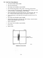
are required in order to guarantee that the position of the read/write heads has stabilized prior to reading.
The timing of Read Data (FM) is shown in figure 1--6.
39238·05
A
B
= LEADING EDGE OF BIT MAY BE
:t: 80008 FROM ITS NOMINAL POSITION
= LEADING EDGE OF BIT MAY BE ±
40008 FROM ITS NOMINAL POSITION
FIGURE 1·6. READ DATA TIMNG (FM)
1-7
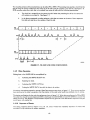
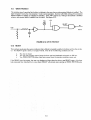
The encoding scheme of the recorded data can be either FM or MFM. FM encoding rules specify a clock bit at the
start of every bit cell and a data bit at the center of the bit cell if this cell contains a one data bit. (see figure 1-7).
MFM encoding rules allow clock bits to be omitted from some bit cells with the following prerequisites:
~~LLS
a.
The clock bit is omitted from the current bit cell If either the preceding bit cell or the current bit
cell contains a one data bit. See figure 1-7.
b.
In the above mentioned encoding schem,~s, clock bits are written at the start of their respective
bits cells and data bits at the centers of their bit cells.
l
..
l~
·_I..__o__
~__o__..__o__..._o
o
DOD
o
0
n....n.JL..n...n
I
I.
~ 2F r--
FM
.J
....,
1F
~",'"
",'
1_.
I
I
II
I
",
/ '"
",'"
,
I
",
~~LLS=
:
I
MFM
/
///
//
0
0
0
[).
.
D.
··IJt.JLJ1----fL.-fl-.n..-n._; ",
tvt
",
1--1F-.f
39238·06
FIGURE 1·7. FM AND MFM CODE COMPARISONS
1.4.9 Write Operation
Writing data to the SA455/465 is accomplished by:
a.
Activating the DRIVE SELECT line.
b.
Selecting the head.
c.
Activating the WHITE GATE line.
d.
Pulsing the WRITE DATA line with the data to be written.
The timing relationships required to Initiate a Write Dalta sequence are shown In figure 1-5. These timinrJ specificatlonsare required in order to guarantee that the position of the read/write heads has stabilized prior to writing.
The timing specifications for the write data pulses are shown In figure 1-8. Write data encoding can be FM or MFM.
The write data should be precornpensated 250 ns starting at track 22 (SA455) or track 40 (SA465) to counter the
effects of bit shifL The direction of compensation required for any given bit In the data stream depends on the pattern It forms with nearby bits.
1.4.10 Sequence of
Event~i
The timing diagrams shown in figures 1-3, 1-4. 1-5. and 1-9 show the necessary sequence of events with
.associated timing restrictions fOli proper operation.
1-8
WRITE DATA
---uJ~
I I.
200 n8 MIN
I,....--8.001'8:t 40
,....-2100 n8 MAX
-.,
nS
I
_I
I _ 4001'8
,....- ±20 ns
FIG,URE 1·8. WRITE DATA TIMING (FM)
POWER ON
~100m.
MOTOR ON
DRIVE SELECT
DIRECTION
,~----------j=. 1 ~. (MIN)
'~~--"1.=i
I
STEP
- - -------,
I~
. .
1 ~.
1
(MINI
y"~- - - - - -
. 11 ~8(MIN)
FIGURE 1·9. POWER ON TO STEP
39238·08·C
39238·12
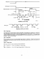
SECTION II
ELECTRICAL INTERFACE
2.1
INTRODUCTION
The interface of the SA455/465 can be divided Into two categories:
a.
b.
Signal Lines
Power Lines
The following sections provide the electrical definition for each line. See figure 2-1 for all Interface connections.
DRIVE
HOST SYSTEM
J1
SPARE SIGNAL, LINE
_.
!
~~,
1'---'
-
1--'
2
SPARe SIGNAL. LINE
DRIVE SELECT 4
-
III
6
DRIVE SELECT 3
12
III
14
--
/7-!
r-t-'
AC
GND
WRITE DATA
III
TRACK 00
TWISTED
PAIR
1---'
1---'
WRITE PROTECT
-
SIDE SELE,CT
21
24
23
25
27
29
32
READY
-
31
34
33
J2
+ 5 VDC:
4
+ 12 VDle
.
3
1
2
rh
"
;
FI(~URE
19
30
"'::..."LOGIC
GND
17
28
-
-
15
26
READ DATA
f4-.
13
22
14-:.'-'
11
20
'-'
f+-.
9
1tJ
WRITE GATE
FLAT RIBBON
OR TWISTED
PAIR
7
16
DIRECTION S:ELECT
.
5
.
MOTOR QIN
STEP
3
10
DRIVE SELECT 2 '
..
1
8
DRIVE SELECT 1
~.
_.
4
INDEx/SECTOR
---
_.
_.
III
2·1. INTERFACE CONNECTIONS
FRAME
GROUND
-~
-
LOGIC
GND
39236·0Q·A
2.2 SIGNAl.. INTERFACE
The signal Interface consists of two categories:
a.
b.
Control Lines
Data Transfer Lines
All lines In the signal interface are digital in nature and either provide signals to the drive (Input). or provide signals
to the host (output). via Interface connector Pl / J 1.
2.2.1
Input Lines
The input signals are of three types: those intended to b,~ multiplexed in a multiple drive system. those which will
perform the multiplexing, and those signals which are not multiplexed and affect all the drives in ?1 daisy chain
system.
.
The Input signals to be multiplexed are:
a.
b.
c.
d.
e.
DIRECTION SELECT
STEP
WRITE DATA
WRITE GATE
SIDE SELECT
The Input signals which are Intendep to do the multlple,<Ing are:
a.
b.
c.
d.
DRIVE
DRIVE
DRIVE
DRIVE
SELECT
SELECT
SELECT
SELECT
1
2
3
4
MOTOR ON is not multiplexed.
..
.
The Input lines have the following electrical specifications. See figure 2-2 for
True
= L<?gical zero = Vln
± 0.0 to + 0.4 V
@
t~e
recommended circuit.
lin = 40 mA (max)
False =togl~al. an'e = Vln + 2.5 to + 5.25 V @ lin =: 250 JlA (open)
Input Imped~nce = 150 ohms
MAX 10 FEET ~
RIBBON OR
. TWISTED PAIR .
-1
-
39238·10
FIGURI: 2..2. INTERFACE SIGNAL DRIVER/RECEIVER
2.2.2 Input Line Terminations
The SA455/465 has been provided with the capablllty of terminating the ten input lines listed below.
1.
2.
3.
4.
5.
DRIVE SELECT
DRIVE SELECT
DRIVE SELECT
DRIVE SELECT
MOTOR ON
1
2
3
4
6.
DIRECTION SELECT
7. STEP
8.
WRITE DATA
9.
WRITE GATE
10. SIDE SELECT
These lines are terminated through a 150 ohm resistor pack. In a single drive system, this resistor pack should be
kept in place to provide the proper terminations.
In a multiple drive system, only the ll:\st drive on the interface is to be terminated. All other drives on the Interface
must have the resistor pack removed. External terminations may also be used. However, the user must provide
the terminations beyond the last drive and each of the five lines must be terminated to + 5 V dc through a 150
ohm. 1/4-watt fCslstor.
2.2.3 Drive Select 1- 4
The SA455/465. as shipped from the f.actory, is conflgureld to operate In a single drive system. The SA455/465
can be easily modified by the user to operate with other drives In a multiplexed multiple-drive system.
In C1 multiple drive system. the four input lines (DRIVE SELECT 1 through DRIVE SELECT 4) are provided so that
the w.. lng system may select which drive on the Interface Is to be used. In this mode of operation. only the drive
with it!; DHIVE SEI.ECT line active will fCspond to the Input lines and gate the output lines.
2.2.4 . Motor On
This Input. when activated to a logical zero level, wilt turn on the drive motor allowing reading or writing on the
drive. A 500 ms delay after activating this line must be allowed before reading or writing. This line should be deactivated. for maximum motor life. if no commands have be:en Issued to the drives within 2 seconds (10 revolutions
of the media) aher completion of a previous command.
2.2.5 Direction Select
This Interface line defines the dlrectlion of motion the read/write heads will take when the STEP line Is pulsed. An
open circuit or logical one defines the direction as out. If a pulse Is applied to the STEP line, the read/write heads
wlll move away from the center of the disk. Conversely, If this Input Is shorted to ground or a logical zero level, the
direction of motion Is defined as In. If l8 pulse is applied tn the STEP line, the read/write heads wilt move towards
the center of the disk.
2.2.6
~tep
Thislnte,rface line is acontrol signal which causes the read/write heads to move in the direction of motion defined
by the DIRECTION SELECT line. This signal must be a logical low going pulse with a minimum pulse width of l/ls
and then logically high for 5 ms minimum between adjaclent pulses. Each subsequent pulse must be delayed by 6
ms (SA455) minimum or 3 ms (SA465) minimum from the preceding pulse.
The access'motion Is Initiated on each logical zero to logical one transition. or at the trailing edge of the signal pulse.
Any change in the DIRECTION SELECT line must be made at least 1 p.s before the trailing edge of the STEP pulse.
The DIRECTION sE.LECT logic level must be maintained 1 JlS after the trailing edge of STEP pulse. See figure 2-3
for these timings.
2.2.7 Write Gate
The active state of this signal, or 10!~ical zero, enables write data to be written on the diskette. The Inactive state or
IOHlcal onc. enables the read data logic and stepper logic. See figure 2-4 for timings.
2:-3
WRITE GATE - - -
~ -
~f-
------
L
DRIVE SELECT - - - - -......
L-
,~
REVERSE
DIRECTION SELECT
I
--..J ..1 pS MIN
STEP
1 ps MIN
--+
I.,..;.....
-l.J1fV
~
1_"""1.·
.'
~
1....
. j.--
5
-.1
1 P.s MIN
....-1 P.s MIN
"'1 P.s MIN
rns MIN
6 rns MIN (SA4551
3 ms MIN (SA465)
39238·11·A
FIGURE 2·3. STEP TIMING
WRITE DATA
I.,
r-F'IGURE 2·4•. WRITE DATA TIMING
400 P.s
±20 ns
39238·12
2.2.8 Write Data
This Interface line provides the data to be: writt~n on the disketh~. Each transition from a logical one to a logical zero
level, wtll cause the current through thE! read/write heads to be reversed thereby writing a data bit. This line is
enabled by WRITE GATE being active. 'Write: dat~ must·be InaiCtlve during a read operation. A write data clamp is
provided on the PCB at the Interface which holds tha" WRITE DATA line at a logical zero whenever WRITE GATE
. Is, .inactlve. See figure 2-4 for timings.
'~
2.2.9 Side Select
jThls signal defines which side of a two-sided diskette 'is to be written on or read from. A logical one selects the side
··O:Head. When switching from one side to the'oth~r:a;100tts delay Is required before a read or write operation can
beinitlated.
:
-;;/~"-
.. -.
·~.~.10
.
. I
',,'
Outpu,t Lines
f.';"':
The output control lines. have the follov/lng
~lectrlCal spe~lflcations.
= 40 rnA (max)
,;rr~e = Logical zero =
+ 0.0 to + 0.4 V@
.false .= lLoglcal one
+ 5 to + 2.5 V (open collector)
I;,~,/."
==
lout
@ lout = 250
2·4
ttA (max)
2.2.11 Track 00
The active or logical zero state of this interface signal Indicates when the read/write heads are positioned at track
zero (the outermost track) and the ac,cess circuitry Is driving current through phase A of the stepper motor. This
signal Is at a logical one level, or inactive state, when thE~ read/write heads are not at track zero. When the
read/write heads are at track zero and anadditlonal step out pulse is issued to the drive, a mechanical stop will
keep the read/write heads at track zero. However, the TRACK 00 signal will go Inactive. This is because the stepper motor wilt go to phase C and not phase A. One more step out pulse wltl put the stepper motor back Into phase
A and the TRACK 00 signal wltl go c:lctlve again.
2.2.12 Index/ Sector
This interface signal is provided by th4a drive each time an index or sector hole is sensed at the Index/Sector photo
detector. Normally, this signal is at a logical one level and makes the transition to the logical zero level each time a
hole is sensed.
When using SA154/164 media (soft sectored). there wltl he one pulse on this Interface signal per revolution of the
diskette (200 ms). This pulse indicates the physical beginning of a track. See figure 2-5 for the timing.
--u-I..
200 ± 4 ma
U
..I
39238·13·A
FIGiURE 2-5. INDEX TIMING (SA154/164 MEDIA)
When using SA155/165 or SA157/167 media (hard sectored). there will be 17 or 11 pulses on this Interface line
,per revolution (200 ms). To Indlcat<:! the beginning of a track, once per revolution there Is one Index transition between 16 or 10 equally spaced sector transitions. The timing for these signals Is shown In figures 2-6 "nd 2·7,
When using the Index/Sector signal, look for an edge or transition rather than a level for determining the status.
, With no diskette Inserted, this signal remains active or at a logical zero level which is an erroneow; status.
12.50 ma
6.25 :1:
0.325 ma
0.5 ma MIN
39238·14
FIOURI: 2..6. INDEx/SECT()R TIMING (SA155/165 MEDIA)
~R9
¥
"I"
SECTOR
S
10~CTOR
I
~.o.o~-I
ms
ma
0.72
2
0.35
39230·15
FIGURE: 2-7. INDEX/SECTOR TIMING (SA1571167 MEDIA)
2.2.13 Read Data
This Interface line provides the raw data (clock and data together) as detected by the drive electronics. Normally,
this signal Is a logical one level and becomes a logical zero level for the active state. Seeflgure 1-5 for the timing
and bit shift tolerance within normal media variations.
2··5
2.2.14 Write Protect
This interface signal is provided by the drive to give the user an indication when a write protected diskette Is instal1~
ed. The signal 15 logical zero level whe~n It is protected. Und4~r normal operation, the drive will Inhibit writing with a
protected diskette Installed In addition to notifying the Interface.
2.2.15 Ready
READY informs the controller that a dlskE~tte Is properly Inserted and that the drive motor Is up to speed. 500 ms is
required for starting the motor and an additional 200 ms is required for one revolution at the rated speed. Thus.
READY is available 700 ms after pow(~r Is applied to the motor. The SA455/465 generates READY by sensing index pulses and measuring their frequency of occurence. When the index pulses are 200 ms apart. READY
becomes active.
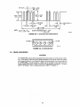
2.3 POWER INTERFACE
The SA455/465 requires only dc power for operation. DC power to the drive is provided via P2/J2. The two dc
voltages. their specifications. and theil: P2/J2 pin designatolrs are outlined in table 2-1. The specifications outlined
on current requirements are for one drive. For multiple drive systems. the current requirements are a multiple of
the maximum current times the number of drives In the system.
T~~BL.E
P2 PIN
DC VOLTAGE
1
+ 12 VDC
2
+ 12 RETURN
3
f 5 RETURN
4
+5VDC
-
i
-
2·1. DC POWER REQUIREMENTS
TOLERANCE
± 1.2 VDC
-
~
CURRENT
1.2 A MAX
0.6 A TYP
MAX RIPPLE (p to p)
50 mV MAX ALLOWABLE
.:!:
0.25 VDC.
0.9 A MAX
50 mV MAX ALLOWABLE
0.6 A TYP
39238·17·A
2.4 FRAME GROUND
It Is Important that the drive be framC:l grounded to the host system ac ground or frame ground. Failure to do so
may result in drive noise susceptibility.
SECTION III
PHY~.I(:AL INTERF:ACE
3.1,,;;JNTRODUCTION
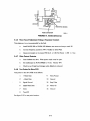
Theefectrlcal Interface between the SA455/465 and the host system Is via two connectors. The first connector.
Jl. provides the signal Interface. The second connector. J2. provides the dc power.
This section describes the physical connectors used on the drive and recommended connectors to be used with
them, See figure 3-1 for connector locatloml.
tCEV
DRIVE
J2
AMP PIN 350211·1
P1 CON NECTOR
SCOTCHFLEX PIN
3463·0001 OR
AMP PIN 583717-5
P2 CONNECTOR
AMP PIN 1-480424·0
FRAME CONNECTOR
AMP PIN 60912·1
FRAME GFIOUND
AMP PIN 61664·1
~92~8·18·A
FIGURE 3·1. INTE:RFACE CONNECTORS PHYSICAL LOCATIONS
3.1.1
J 1 / P1 Connector
Connection to J 1 is through a 34 pin PCB e:dg~~ connector. The dimensions for this connector are shown in figure
3-2 .. The pins are numbered 1 through 34 with the even numbered pins on the component side of the PCB. The
oddnumbered pins are on the non-component side. Pin 2 is located on the end of the PCB connector closest to
thesorner and is labeled 2. A key slot Is provided between pins 4 and 6 for optional connector keying.
3.1.2 J2/P2 Connector
The dc power conhector. (J2. is a 4 pin AMP Mate·N-Lok connector (PIN 350211-1). The recommended mating
contierlm. P2. is AMP PIN 1-480424·0 usin~J AMP pins PIN 61473·1. J2. pin 1. Is labeled on the component
side of the PCB. Wire used should be 1118 AV·iG. Figure 3-3l\1ustrates the J2 connector as seen on the drive PCB
from the non -component side.
3-1
KEY sLor--II--'0.036 ± 0.004
(0.9 ±
......
f
0.1~
~~
.1
0.450 ± 0.010
(11'j ± 2.5)
t
0.40 ± 0.010
(10.2 ± 0.3)
II
::
L-............. _-..........-""----_~~~
_ ~-:i1=O.O~~.~OM ~
1.795 ± O.l)05
(45.6 ± 0;13)
BOARD THICKNESS 0.062 ± 0.007
(1.6 ± 0.2)
, _ (1.3)
.......
11--
NOTE:
~0.1JM
x.xx ± x.xx = In.
(x.xx ± x.xx) = mm
(2.5)
r---0.063 NOM (2 x)
(1.6)
::
39238·19
FIIGURE 3·2. J1 CONNECTOR DIMENSIONS
+ 12 VD(~
+5VDC
39211·16
FIGURE 3·3. J:2 CONNECTOR
3.2 FRAME GROUNDING
CAUTION
The SA455/465 must be frame grounded to the host system to ensure proper operatlon. If the frame of the: drive Is not fastened directly to the frame of the host system
with a good ac ground, a wire from the system ac frame ground must be connected to
the SA455/465. For this purpose, a faston tab is provided on the drive near the
motor control PCB whe:re a faston connecj~or can be attached or soldered. The tab is
AMP PIN 61664-1 and its mating connector Is AMP PIN 60972-1.
3-2
SECTIO:N IV
THEORY OF OPERATION
4.1
THEORY OF OPERATION
The SA455/465 floppy diskette driv·e electronics are packaged on one PCB which contains:
a.
b.
c.
d.
e.
f.
g.
h.
I.
Read/Write Amplifier iand Transition Detector
Spindle Motor Control
Drive Select Circuits
Index Detector Circuit!;
Track Zero Circuits
Track Accessing Circuits
Power On Reset Control
Write Protect Circuits
Drive Status Clrc:ults
The head positioning actuator move's the, read/write head (5) 'to the desired track on the diskette. The head (5) Is
loaded onto the diskette when the c100r Is closed.
The following paragraphs describe €~ach of the above functions In detail.
4.2
READ/WRITE OPERATIONS
a.
The SA455/465 uses the double frequency non return to zero (NRZ) recording method,
b.
The read/write head, In general. Is a ring with a gap and a coil wound at some point on the
ring.
c.
During a write operation. a bit Is recorded when the flux direction in the ring Is reversed by
rilpldly reversing the current In the call.
d.
During a read operation. a bit is read when the flux direction In the ring is reversed as a result of
a flux reversal on the! diskette surface.
The SA455/46[) drives use the double-frequency (2F) longitudinal NRZ method of recording. Double frequency IS
the term given to the recording system that Inserts a clock bit at the beginning of each bit cell thereby doubling the
frequency of recorded bits. This clock bit. as well as the data bit. is provided by the using system. See figure 4-1,
'D
CDC
C
C
CDC
CDC
JlJ1..J1J1....f'1-..fL.
.
BIT CELL 0
BINARY
REPRESENTATION
HEX
REPRESENTATION
1
\
BIT CE,LL
-
-
~
1
"------
- -
..... r---
"-
BIT CELL 2
BIT CELL 3
BIT CELL 4
BIT CELL 5
BIT CELL 6
BIT CELL 7
0
o
1
0
1
0
./\~---......,.------/
I
39211·17
r
c
A
FIGURE 4·1. BYTE
4·1
4.4 WRITE CIRCUIT OPERATI'ON
a.
The write data trigger flips with each pulse on the WRITE DATA line.
b.
The write data trigger alte:rnately drives one or the other of the write drivers.
c.
WRITE GATE allows write current to flow to the write driver circuits If the diskette is not write
protected.
d.
Write current sensed aUows erase coil current.
e.
Heads are selected by grounding the appropriate center tap.
WRITE DATA pulses (clock and data bits) are supplied by the using system. The write trigger "flips" with each
pulse. The outputs are fed to alternate write drivers.
WRITE GATE and NOT WRITE PROTECT are ANDed together and will cause write current to flow to the write
driver circuits. which In turn causes the center tap switch to dose and erase current to flow after the turn on delay of
400 J.tsec.
The output of one of the write drivers allows write cutrent to flow through one half of the read/write coil. When the
write trigger "flips." the other write driver provides write current to the other half of the read/write coil.
The removal of WRITE GATE causes the turn off delay circuit to time out for 1.1 ms. At the end of the delay. the
center tap switch opens and the eral>e current source Is turned off. See figure 4-7.
~
n
I
5V
10
12 0
~"",1>--6_ _
11_1 T
~
Q
98
R Q
~
DP3
DAP201
j--::- -,
M002W1r
R55 M001Wr
9 ; ....~I--..-----...--~l:
~--t-"f-+--+--+_-.....-~_LJ
.•, ,
4.7 K
4
IlA56
jJ__
~U- ~7K
DP1
DAP201
• _. --,
I
5
I ;- ---ll<-'~'-~'
6:
13
:
LaJ-+I~--+-+--f-"":'---+-M1l-'
7 }._~::
12A
8
~-_:
I
;-:9 RW10
,,-_~.4
150 1 %
14
5
RW20
6
RW11
R54
RW21
1
751%
t--'--5V
,13
ERASE 0
12
C31
1
C32
T
4
ERASE 1
3
GND
~
4
12 GND
,
~'_---+-+-:--'_--W.-.!-
H 0 0 CT
1......----,--W-fL HD 1 CT
t-4---_.--:--.......
118
1--..JV\I\r----:.---'-.-'V\.1'V-t~12 H A
2
1445
FIGURE 4~·7.WRITE CIRCUIT
~
~1
NC
GND
-3~239.01
4.5 READ CIRCUIT OPERATION
a.
Duration of all read operations is under control of the using system.
b.
As long as the drive i:s selected and WRITE GATE Is not active, the read signal Is amplified and
shaped and the square wave signals are sent to the Interface as READ DATA.
When the using system requires data from the dlsketh! drive, the using system must select the head and disable
WRITE GATE. The read signal lis then fed to the amplifier section of the read circuit. After amplification. the read
signal Is fed to a filter where the~ out of band noise is removed. The read signal Is then fed to the dlfferentiator
amplifier.
Since a clock pulse occurs at least once every 8 p.s and data bits are present once every 4/A.s, the frequency of the
READ DATA varies (FM encoding only), The read signal amplitude decreases as the frequency increases. Note
the signals in figure 4-8. The dlflfere!ntlal amplifier will amplify. differentiate. limit. and digitize the read signals (sine
waves).
The drive has no data separato:r. only a pulse standardizeI' for the READ DATA signal.
ERASE 1 - ERASE 0
r
...,
+ 12V
-1+--
I
I
SIDE 0
I
I
rSIDE 1
I
I
I
---.-.. . -+
+ 5 V REG
'----+-+---1-+
I
L__
l.-.ot----f
"----,----4
LSI
READ
CH IP
+ READ
ENABLE
- READ DATA
39211·24
SELECT1------~
SELECT 0 - - - - - - '
FIGURE 4·8. READ CIRCUIT
4.6
DRIVE MOTOR CONTROL
a.
b.
c.
d.
Start/Stop
Speed Control
Over Current Protection
Speed Adjustm,mt
The motor used in the SA455!',l~65 is a de drive motor with a separate motor on and off interface line. After ac·
'tivatlng the MOTOR ON line. a 500 ms delay must be introduced to allow proper motor speed before reading or
writing.
When MOTOR ON Is activated at: pin 16 of the Interface. the mode will start by means of current flow through the
motor windings. The motor speed control utilizes an integral brushless tachometer. The output voltage signal from
this tachometer is compared to a voltage/frequency reference level. The output from the voltage/frequency comparator will control the necessary current to maintain a constant motor speed of 300 rpm. Motor speed adjustment
.
changes the voltage reference! through a potentiometer.
4·5
4.7 INDEX DETECTOR
Each time an index or sector hole is moved past the index photo detector, a pulse is formed. This pulse is present
on the interface as index/sector pin 8. Without a diskette in the drive, the output line will be low and the using
system must look for a transition to be a valid signal. The detector output is fed into a schmidt trigger with a level
trigger latch back to maintain pulse stiabillty while shaping the pulse. With output enable true, this pulse will be on
the interface as a negative going pulse. See figure 4-9.
+5V
22
TP7
•
-.
-INDEX
SECTOR
-SELEC:T'---------<-..
39239·21
FIGURE 4-9. INDEX DETECTOR
4.8 TRACK ZERO INDICATION
Track 00 signal (pin 26) is provided ttD the using system to Indicate when the read/write head is positioned on track
00. The track 00 indication is provided when the flag attached to the head carriage passes between the photo transistor and the photo detector. On tr2lck, DRIVE SELECT Is ANDed with the photo detector output. These conditions will cause a track 00 indication to the Interface.
4.9 TRACK ACCESSING
a.
b.
c.
. d.
Stepper Motor (Four Phase)
Stepper Control Logic:
Reverse Seek
Forward Seek
Seeking the read/write head from one track to another is accomplished by selecting the desired direction utilizing
the DIRECTION SELECT interface line:, loading the read/write head, and pulsing the STEP line. Multiple track
;, accessing is atcompllshed by repeah!d pulsing of the STEP line with WRITE GATE Inactive until the desired track
has been reached. Each pulse on the STEP line will cause the read/write head to move one track either in or out.
depending on the DIRECTION SELECT .1Ine.
4.9.1 Stepper Motor
The four phase stepper motor turns thc2! head actuator cam in two step Increments per track for the 455 and one
step Increments for the 465. The band actuator and capstan move the heads track to track.
Two current modes are automatical!ly enabled, The first step pulse will enable full current to the stepper motor.
;Within 35 ms after that last step pulse is Issued, stepper motor current Is automatically decreased to approximately
50% of its full value.
;4.9.2 Stepper Control
During power on reset time, the stepp~~r control counter is reset to zero. This causes phases -B and -A t6 be
energized In the stepper. Figures 4-10 and 4-11 show the stepper control logic and timing.
4-6
DIRECTION
SELECT
1---
---I t:::::'5OO ns MIN
---===tJ-----.
-...J (....--
----.11.---1
1 itS MIN
STEP~-U
-:it-
1 itS MIN --'..
~
•.
6 me MIN (SA455)
its
MIN
u
U
39239·03
3 me MIN (SA465)
FIGUAE4·10. STEPPER TIMING
+5V
+5V
ERO
ER1
T
-
FIGURE 4·11. POWER ON RESET
39239·22
4.10 DRIVE SELECT
The SA455/465 is configured to oplar~te alone In a single drive system. It can be easily modified to operate with
other drives in a daisy chained multiplexed drive system. This Is done by selecting the specific drive address and
jumperlng the appropriate DRIVE SELECT line. See figure 4-12.
The "MX" option Is used for sln~!le drive systems. By shorting HMX. the I/O lines are always enabled.
1l
The "MS" option allows the mot~:>r to be enabled from DRIVE SELECT.
+5V
OS1
)(
6
2
X
14.:.-
3
X
12
4 )(
10
~
OS
MX
{>
?
FIGURE 4·12. DRIVE SELECT
4-7
SELECT
39239·23
4.1'1
WRITE PROTECT
This interface signal is provided by the drive to Indicate to the user when a write protected diskette is installed. The
signal is logical a level when it is proltected. Under normal operation, the drive' wil1lnhlbit writing with a protected
diskette Installed In addition to notifying the Interface. If the uWP" trace Is cut, writing to the diskette is Inhibited
unless a write protect label Is installc:!d over the notch. Sc:!e figure 4-13.
+5 V
TP9
-b D
:>---+--.
-wp
SELECT.
D-_2_839239·24
FIGURE 4·13. WRITE PROTECT
4.12 READY
This Interface signal gives the user an Indication that a dlsl<4ette Is Inserted correctly In the drive and the door is closed. The READY signal Is active. a1 a logical 0 level. wh,m all of the follOWing conditions are met:
a.
b.
c.
The door is closed.
The door has not been opened since the drive was last deselected and timed out 500 ms.
Two INDEX/SEeTOn pulses have been sensed since the previous conditions were met.
If the READY signal is inactive:. the user may deselect and then select the drive to test READY again: if the door
had previously been disturbed but is nc>w closed. READY wl11 activate upon sensing an INDEX/SECTOR pulse.
4·8
SECTION V
MAINTENANCE
5.1 MAINTENANCE
EQUIP!~ENT
5.1.1 Alignment Diskette
The alignment diskette is used for verifying and adjustlt1ig the SA455/465. Two alignment diskettes are available.
The SA455/465 has two read/wlite heads and requires written information on both surfaces. The SA128 (48 tpi)
alignment diskette should be used when performing seJ'1l1ice checks on the SA455. The SA465 requires the SA126
(96 tpi) alignment diskette.
The following adjustments and checks can be made u:sing the SA128/126 alignment diskettes.
SA455·SA128
SA465·SA126
TRK 33
TRK 64
Set at TRK 38
Verified at TRK 01
Set at TRK 76
Verified at TRK 02
a.
Read/Write Head Radial Alignment
b.
Index Photo Detector Alignment
c.
Track 00 Head Po-sitic)n
TRK 00
TRK 00
d.
Azimuth Anale (not field adjustable)
TRK. 33
TRK 64
e.
125 k Hz Signal R.ecorded to Check
Head Position on Inside Track
TRK 34
TRK 79
Caution should be used not to de:stroy prerecorded alignment tracks. The write protect tab must be installed to prevent accidental writing on the alt!~nl1nent diskette. If the write protect option Is used, remove the write protect tab.
5.1.2 Exerciser PCB
The exerciser PCB can be used in ja stand alone mode. built Into a test station. or used In a test for field service.
The exerciser wilt enable the uset to make all adjustme:nts and check outs required on the SA455/465 minidlskette
drive. It has no Intelligent data handling capabilities but can write a 2F 125 k Hz signal which is the recording frequency used for amplitude checl<s c~nthe SA455/46S drive. The exerciser can start and stop the drive motor. and
enable read in the SA455/465 to allow checking for proper read back signals.
5.1.3 Special Tools
The following special tools are available fo,r performing malnten,ance on the SA455/465.
Description
Part Number
SA128 Alignment Diskette
54573
SA126 Alignment Diskette
54382
, Exerciser PCB
54157
Head Cable Extender
54578
Phillips Screw Drivers
Medium and Small
Oscilloscope
Textronbt 465 or equivalent
5,.,2 DIAGNOSTIC TECHNIQUES
5~2.1
Introduction
Incorr~ct operating procedures, faulty progll'amming, damaged diskettes, and ~~soft errors" created by airborne contaminants, random electrical noise. and other' external causes can produce errors falsely attributed to drive failure
or,mlsadjustment. Unless visual Inspection of the drive discloses an obvious misalignment or broken part. attempt
to' repeat the fault with the original dlskett:e. ~hen attempt to duplicate the fault on a second diskette.
5.2.2 "Soft Error" Detection and Cc)rr.!ctlon
S6ft errors are usually caused by:
a.
Airborne contaminants that pal~S between read/write heads and disk. Usually these contaminants
can be removed by cartridge self"cleanlng wiper.
b.
Random electrical noise th2tt usually lasts for a few microseconds.
c.
Small defects In written dat.!' and/or track not detected during write operation may cause soft errors during read.
d.
Improper,groundlng of power supply. drive, and/or host system. Refer to SA455/465 OEM
manual (P /N 39238) for PI'op42r'groundlng requirements.
e.
Improper motor speed.
The.folloWlng procedures are recommended to recover from the above mentioned soft errors:
a.
Reread track 10 times or u1,tll such time as data Is recovered.
lfdata Is not recovered aftEir using step (a), access head to adjacent track In same direction
previously moved. then return to desired track.
5'.2~3
j,
c.
Repeat step (a).
d.
If data Is not recovered. en-oris not recoverable.
Write Error
Ifan:error ,occurs during a write operation,. it wHl be detected on the next revolution by doing a read operation.
commonly called a "write check."To COlrrect the error. anothe:r write and check operation must be done. If the
write operatlonlsnot successful after 10 attempts have been made. a read operation should be attempted on
another track to determine If the media or the drivels falling. If the error persists, the diskette 'should be replaced
and the above procedure repeated. If the: fallure 'still exists, consider the drive defective. If the failure disappears.
'
cbnslder the original diskette defective and discard It.
5.2.4 Read Error
Most errors that occur will be Hsoft enors." In these cases, performing an error recovery procedure will recover the
data.
5.2.5 Seek Error
a.
Stepper malfunction.
b.
Carriage binds.
c.
To recover from a seek error, recalibrate to track 00 and perform another seel< to the original
track or do a read ID to find on which track the head is located.
5.3 TROUBLE-SHOOTING
Figures 5-1 through 5-5 provide tr,ouble-shooting procedures for the SA455/465.
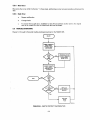
~.,.AR_T_..,."
INSERT DISKETTE
WITH WRITE
PROTE:CT SLOT
UNCOVERED
NO
PERFORM WRITE
PROTECT SENSOR
ADJUSTMENT
(PARA. 5.4.7)
INSERT DISKETTE
WITH WRITE
PROTECT SLOT
COVERED
REPLACE
WRITE PROTECT
SENSOR
\1
YES
REPLACE
DRIVE
PCB
'"-
FI(~URE 5·1.
WRITE PROTECT INOPERATIVE
5-3
3923904
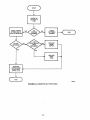
G~
[
I~D..
'--C-H-ECK
VOLTAGE: AT
PCB
rCHECK JUMPER
OPTIONS AND IF
DRIVE IS SELECTED
YES
NO
CHECK
DC POWER
SOURCE
END
REPLACE
DAIVE
MOTOR
REPLACE
DRIVE
PCB
PERFORM
MOTOR SPEED
ADJUSTMENT
(PARA. 5.4.1)
39239-05
FIGURE~ 5-2. DISKETTE NOT ROTATING
5-4
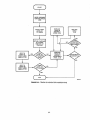
C
START
~-,- --...
:VE
CARRIAGE
rOWARDS TRACK
39/79
......
[-
::~ECK
~
STEP TO
TRACK 01
CHECK LOGIC
LEVEL AT TP7
YES
REPLACE
TRACK 00
ASSEMBLY
(PARA. 5.5.9)
LOGIC
LEVEL AT
TP7 (ZERO)
;URN CARRIAGE
REPLACE
DRIVE
PCB
NO
"0 ITS REST
P'OSITION AT
TRACK 00
NO
PERFORM
TRACK 00
ASSEMBLY
ADJUSTMENT
(PARA. 5.4.5)
YES
STEP TO
TRACK 00
CHECK LOGIC
LEVEL AT TP7
39239·06
FIGURES-3. TRACK 00 INDICATOR INOPERATIVE
5·5
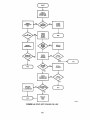
CHECK
BOARD FOR
DC VOLTAGE
CHECK
TERMINATOR
1500
NO
YES
CHECK
~
DRIVE
SELECT
JUMPER
.]
END
NO
INSTALL
TERMINATOR
CHECK
JUMPER
OPTIONS
CHECK
POWER
SOURCE
INSTALL
JUMPER
NO
NO
END
NO
END
CHECK
1/0 CABLE OR
INSTALL
JUMPERS
NO
CONTROLLER
YES
REPLACE
I/O CABLE
& CONTROLLER
END
REPLACE
DRIVE
PCB
.1923!).Ol
FIGURES,,4.IDRIVE NOT COMING ON LINE
5·6
START
CHECK TO
seE IF DISKETEE
IS PROPERLY
INSTALLED
YES
CHECK
DISKETTE
ROTATION
-
CHECK
00 POWER
SOURCE AND
[~NECTOR
YES
YES
AT J2
END
CHECK TP7
FOR PULSE
200 Msec
REPLACE
C..__
INDEX/SECTOR
NO
PHOTOTRANSISTOR......._ _ -<
ASSEMBLY
(PARA. 5.5.6)
EN_D
_ _,.,
C
TURN DISKETTE
OVER REINSERT
r-{---
END·
"'------
---PERFORM
DI'SKETTE
NOT ROTATING
(FIGURE 5·2)
C,,--EN_D)
PERFORM
INDEX/SECTOR
ADJUSTMENT
(PARA. 5.4.6)
\9?19·0fl
FIGURE 5-5. INDEX PULSE INOPERATIVE
5·7
t
5.4 ADJUSTMENTS
5.4.1
Head Radial Allgnment
NOTE
The SA465 r~ad/wrlte h,!ad assembly is aligned at factory and adjustment of head to
head alignment is not field adjustable.
a.
Insert alignment diskette (SA455 = SA 128) (SA465 = 126).
NOTE
Alignment diskette should be at room conditions for at least 24 hours before alignment
checks.
b.
Select drive and step head(s) to track 16 (SA455) or track 64 (SA465).
c.
Sync oscllJoscope external nc!gative on TP7 (- INDEX). Set time base to 20 msec per division.
This will display over one revolution.
.
d.
Connect one probe to TP1 and other to TP2. Ground probes to PCB. Set inputs to ac, ADD,
and Invert one channel. Set vertical deflection to 50 mV/dlvlsion.
e.
Amplitude of two lobes must be within 70% of each other (80% for 465). If lobes do not fall
within specification, continue on with procedurc! (see figure 5-6).
100 mV
20 msec
100 mV
-j-
-.
20 msec
-f
EQUAL
AMPLITUDE
100%
AMPLITUDE
DIFFE:R'ENCE
MUST BE
WITHIN 70%
39239·25
FIGURE 5·6. ALIGNMENT LOBES
f.
Loosen two mounting screws, which hold steppc~r motor to base casting (see figure 5-7).
g.
Adjust stepper motor"
h.
WhC?n lobes are of equal amplitude, tighten motc:>r plate mounting screws (see figure 5-'7).
I.
Checl< adjustment by stepping off track and returning. Check In both directions and readjust as
required.
j.
Whenever head radial alignmc:mt has beehadjusted, track 00 detector must be checked
(paragraph. 5.4.4).
5-8
CAUTION
When tlght~mlng mounting screws, pressure must be applied to the rear of the step
motor through the rectangular hole In the side of the casting to keep the motor bracket
against the registering surfaces of the casting. Failure to do this will angle the band
positioner causing track-to-track problems.
MOUNTING SCREWS
39239·09
I=IGURE 5-7. STEPPIER MOTOR MOUNTING SCREWS
a.
Install alignment dlsl<ette (SA455 = SA128) (SA465 = SA126).
b.
Select drive and step to track 33 (SA455) or track 64 (SA465).
c.
Sync oscilloscope external neUi'ltlve on TP7, set lime bast' to 0, G m!.;(lC
d.
Connect on(~ probe to TPl and other to TP2, Invert one channel and ground probes to PCB.
Set inputs to ac. ADD. and 50 mV per division.
e,
Compare waveform to figure 5·8. If not within range shown. replace read/write head assembly.
5·9
pOl'
division,
50mV
50 Jtsec:
50,tsec
50 mV
AZIMUTH
+ :~1 MINUTES
AZIMUTH
o MINUTES
50mV
AZIMUTH
-18 MINUTES (SA455)
-21 MINUTES (SA465)
50 mV
39239·10
FICJURE 5·8. AZIMUTH CHECK
5.4.3 Head Amplitude Check
Ith~se.·.·.CheckS are.. only valid when writing and reading back as described below. Ensure the diskette used for this
t'check}s not "worn" or otherwise shows evidence of damage on either side.
a.
Install good media.
b.
Start motpr.
c.
Select drive and step to track. 39 (SA455) or track 79 (SA465).
d.
Sync oscilloscope external on TP7 (+ Index); connect one probe to TP2 and TPI on drive PCB.
Ground probes to PCB, ADD, and invert one input. Set volts per division to 50 mV and time
base to 20 msec per division.
e.
Select head a and write a 2F pattern on entire track. Average minimum amplitude peak-to-peak
should be 100 mV.
f.
Select head 1 and write a 2F pattern on entire track. Average minimum amplitude peal<-to-peak
should be 100 mV.
g.
If either head falls to meefmlnlrnum amplitude spe!clflcatlons. continue with procedure.
h.
Install fresh media andrecheck.
i.
Checl<motor speed as per pi:uagraph 5.4.6.
j.
With oscilloscope In"chop" rnode,:verlfy that output exists atboth TPI and TP2. If one TP has
no output. or significantly les~.output than other turn head cable connector over at J4. Should
same TP have little or no output, pes Is faulty and needs replacing. If opposite TP now exhibits
problem, head assembly Is atfaulLand should be replaced. Refer to paragraph 5.5.3.
I
5·10
5.4'.4 Track Zero Detec:tor A~ssll!mbly AdJustmelllt
a.
Apply power to drive and Install alignme:nt diskette SA128 or SA126.
b.
Select drive and
c.
Sync oscilloscope
d.
Connect one prob,~ tOI TPI and other to TP2. Ground probes to PCB. Set input to ac, ADD,
and invert one cha,nn,~1. Set vertical def'lectton to 100 mV/divlslon.
e.
The 125 k Hz signal recorded should be: observed at this time.
f.
If 125 k Hz signal is not present. step forward one track at a time and verify 125 k Hz signal is
present. Step
st4~P 1:0
track 00.
,~xternal
onl~,
negative on TP7 (-Index). Set time base to 20 msec per division.
five tracks.
g.
Step back towards track 00 detector and verify presence of 125 k Hz signal. Repeat stepping
untlJ signal Is found.
h.
Once 125 k Hz sl~~nalls present on oscllloscope. carriage Is located at track 00. Disconnect probes from TP1. TP:2, and TP7. Conned one channel to TP8 and set input to de. Set vertical
deflection to 2 V per division. Trigger oscilloscope on selected input channel.
I.
Step to track 01 a'nd verify that TP8 goes to zero.
j.
If not, loosen tradt 00 bracket.
k.
Set drive to seek
I.
Adjust eccentric until a 50% duty cycle Is obtained (see figure 5-9).
m.
Tighten track 00 bracket and recheck timing.
n.
If same signal is obtained, remove alignment diskette, power down drive, and reinstall PCB. If
same signal
115
c~ltelmately
between tracks 00 and 01.
not obtained, repeat steps k-n.
MOUNTING
SCREWS
MOUNTING
BRACKET
39239·12
FIGURE 5-9. TRACK ZERO ADJUSTMENT
5-11
5.4.5 IndexlSector Timing AdJu8tme!nt
a.
Insert alignment diskette SA128 or SA126.
b.
Start motor and select heald O.
c.
Step carriage to track 01 (SA455) or track 02 (SA465).
d.
Sync oscilloscope external positive on TP7 (+ Index). Set time base to 50 J,tsec/dlvlsion.
e.
Connect one probe to TPl and other to TP2. Ground probes to PCB. Set Inputs to aCt ADD.
and invert one channel. Set vertical deflection to 500 mV/dlvlslon.
f.
Observe timing between start of sweep and first data pulse. This should be 200 + 200/ -100
J,tsec. If timing Is not within tc)lerance, continue on with adjustment. See figure 5·10.
g.
Loosen mounting screw In Index detector block until assembly Is just able to be moved. See
figure 5·11.
h.
Step carriage to track 38 (SA455) or track 76 (SA465).
i.
Observing timing, adjust detector until timing Is 200 + 200/ -100 J,tsec. Ensure that detector
assembly is against registrcltlol"\ surface on hub fl:ame.
j.
Tighten mounting screw.
k.
$tep carriage to track 01 (SA455) or track 02 (SA465).
I.
Recheck timing.
m.
Repeat for head 1.
50 mV
50 Jtsec
.....-+--'t-~
~
_-..-I~I_ _+--I--t INDEX BURST
I
I
I
200/tsec ± 100/tsec
_--,--_....__.._.._-----
.....
50 mV
IFIGURE 5·10. INDEX BURST
5·12
39239·13
INDEX oe'rEctOR
39239,14
FIGURE 5-11. INDEX DETECTOR
5.4.6 Motor Speed AdJustll1le,nt (Using a Frequency Counter)
This adjustment is not recommended for the field.
a.
Install SA128/1~~6 c)r SA154/155 disl(ett~; start motor and step to track 32.
b.
Connect frequ~ncy counter to TP7 (+ Inde)() on drive PCB.
c.
Adjust pot located on the motor PCB for 5 ± 0.05 Hz (Period = 200 ± 2 ms). ,
5.4.7 Write Protect Detec:tol'
a.
Insert diskette in1:0 drive. Write proted notch must be open.
b.
Set oscilloscope to AUTO SWEEP. 2 V/div. Monitor TP9.
c.
Check to see If IIOgic'level changes when diskette Is removed.
5.4.8 Test Points On DrI"te ItCD'
Test points for the drive PCB ,are ,as follows:
1
+Read Data
9
Write Protect
2
-Read Data
10
Ground
5
Signal Ground
12
Step Pulse
6
Digital Read Dai:a
13
Motor On
7
Index
15
Ground
8
Track 00
See figure 5-12 for test point :locations.
5-13
39239-18
FIGURE 5..12. PCB COMPONENT LOCATIONS, PIN'S 25284 AND 25286
5·14
5.5 REMOVALS AND REI)LACEMENTS
5.5.1 Faceplate Latch
a.
Open door. Remove door latch.
b.
Remove mounting screw on each side of faceplate. Pull faceplate forward and away from drive
casting.
c.
No re-adjustment is required after replacement.
5.5.2 Direct Drive Motor ASlsembly
This assembly is not recommend~!d for field replacement.
5.5.3 Head and Carriage Astsembly
This assembly Is not recommendE~d for field replacement.
5.5.4 Stepper Motor and ACltuator Assembly
This assembly Is not recommendE!d for field replacement.
5.5.5 Clamp Hub
5.5~6
a.
Remove PCB.
b.
Open door.
c.
Remove clamp clssembly front andrectr screws.
d.
To reinstall: Pc~slti4:>n hub clamp with spacer and spring in place onto spindle hub. (Large end
of spring Is plac~~d against hub frame.)
e.
Press hub frame down towards splndl4~ until hub shaft protrudes through mounting hole in hub
frame.
f.
Reinstall faceplate. Re'adjustment Is not required.
Write Protect Sensor lund Index Detector
a.
Remove connec'torfrom PCB.
b.
Remove mounting screw from write protect assembly. This will free assembly.
c.
Remove Index detectbt screw to free detector.
d.
Reverse Instructions to reinstall.
5.5.7 Track Zero Photo D'etector
a.
Remove PCB and shields from drive.
b.
Remove:
c.
Loosen mounting bracket screws.
d.
Remove two screws securing LED housing to track 00 plate.
e.
To reinstall,
f.
Adjust as directe!d 111 paragraph 5.4.5.
white! wire from J6 Pin 2.
green wire from J6 Pin 1.
yellow wire from J6 Pin 10.
rev~~rse
above procedure.
5·15
6.6 RECOMMENDED INCIOMING RECEIVING INSPECTION
6.6.1
Necessary Equlpmen,t
All Shugart drives are 100% adjusted and tested befor'e leaving the factory.
ping damage on receipt of' drivc;!s.
It is only necessary to inspect for ship
Inspection should be simple and test equipment kept to a minimum. Shugart recommends the following equIpment.
a.
SA809 Exerciser (PIN 54157)
b.
Exerciser InstrucUon Manual (PIN 50686)
c.
Power Supply for Exerciser and Drive (+ 5, +12 V)
d.
Oscilloscope
e.
SA128/126 Alignment Diskette
f.
SA455/465 Service Manual (PIN 39239·0)
5.6.2 Procedure
a.
Unpack drive andl inl;pect for physical shipping damage.
b.
Make sure all power is off.
c.
Attach exerciser cables to appropriate drive connectors.
d.
Power up.
e.
Insert alignment dlsk'2tte (SA455
f.
Set track addressc~s of 00 and 39 (SA455) or 79 (SA465) into exerciser.
g.
Select drive.
h.
Start motor and 14~t drive seek automatilcally for 5 minutes.
= SA128, SA465
= SAI26).
I. '\ Check that activity light is on.
j.
Using this SA455/465' Service Manual and the Exerciser Instruction Manual as guides. perform
the follOWing cheeks:
'.
Index timing Adjustment (paragraph 5.4.6).
•
Head Radial Alignment, Sides 0 and 1 (paragraph 5.4.1).
•
Track Zero Switch is on at track 00 and off at 01 and 02.
k.
Remove alignment diskette and insert SA154/155 diskette.
1.
Seek to track 39 (SA455) or track 79 (SA465) and write a 2F signal. Minimum read back
should be 90 mV.
m.
Check write prot<;~ct sensor adjustment (paragraph 5.4.8).
n.
Power off.
o.
Remove connectors and repack drive.
thIs procedure verifies that the crltic;al functlonsof the drive are working properly (i.e .. the drive will read and
write, the disl< will rotate atthe prop~r speed, and critical adjustments are within specification).
5-16
'#+'2
iOJtI·i
•
MY
Ie,
onCRIPTIOH
I
IZV'-'
"
HAI~'P
R4Z
ylPI
~ ~~I"'18_"';;'5o-o--"~4_ _-'AV~VlA-",__.., LG
'sv
liT
~~OJlt
O.IUf
IIA
(.21
'JW 114
I
150Pf
O.I~f
~qoSl
U
TP5
r'
{Z.2K 15
C20
h~'4.---4t", .9_~7.1J-1
. ~~rJ-"o(;_ _~Rv4.""A.,.....l_--,
0.1
.~R4~ ~18
lSOUH
T
7~;)O
.......~....-+--..
~:pr....
>R44
.>2.ZK
150UH
-+ .
~2:-r--AR1-~-C2-2-i.IeJOOPf-_-~-L-4--'~~
,
bTP2
200
rFA"T;'~LAH
'4f(
TPl5
;h
;~ WI 20K
R45 "
)
~>
10t\
f2V --W;-'2V(GV)
....-------------.-0..
~
..;(---;.-..---------===-~--5vr+/-+,---<li;
ITt:
24
J(
D'J6
It P
...-
';;,:~
J;: ;:
7
IG
5
~ g.
a
~1.1
.:)IeoE-
n
•
5
R~
~
..----~<D-cL'JI'"4":":B~;j....4\......--"1--."...9~"',--::';;II'V"
5V --""IOOK"""......ooI\ff..A~I\...........+-+-----~---..
Q..21\
:>1\0 "
~8"'7A
---1'
~~
~nWJ:lV'LRz
~11\
91
1_ 5
~~;!)
'(),,,~Of'fift CA)
~
rnptpr~;):
,}
R~:t1K
66
R
e"l-----''?
rO
oW- MDHLD
~O-@
fl~'
ItT-
15 MD2
~
14
I
5V
~.
Ht._
J
~-----: . . 5VPC"
4
6'11O';'~
GNO
2....
LI
1+(1
1.7Uf_TZ5V
z~
l.
'V
I
+'2.vOG~i
TOA,O'
t
5V
,
4.7Uf
ll-r---....
" A
;]001
..QOOl.L-C7
SMD'
04
, .12V
J
-. 6
- f
5V
Q
+05
JZ
18
36
'
~
-
G
_-L.-...
qn
5J~ ~
---lY'
------~~ ""
----IT
R
39
•
e
+5;-JQ}~
-t6
74045
118
74tS74
(DB qf)
75452
,M
75-15'!)
41\
75'-77
51\ Gi'\
7...tS240
28
s~ee"
5f>(214)
,~ 12:~?~,¥,~~:
jl
7~
elG
2i::::::
i
2r- - - -
I "
~RDY
R"2
150
R~T ~nl
1 GH -
- 10
,
~
RR
~
_ 121' TIt7
VDD
~5
~
lOo~T
.... CI5
T
--n-;
t
·5V
OPEN
MD~
~ttORT
MD4
OPE:N
NOT U5E:O
R57
R23,R24,R27
C28
eRG
CR2), CR4
05
QI,O€
TPH5
". "'.11. ,.,
_
~V
.. "
~ 515=
t7"7b v
DMACT
L::.....:J
DR\.~IIA~X),..~G----_f_-...,r.:2".;:;,...;:-TRl\CKzeRO
q JQ.IIIA~n.:;e;...., ----....-~1__=o8...;z-'NDEX
:~1T;,-II I£T1VllY
28 -WRITe PROTECT
.--~---i""-'-IL'!..~r
,
~~ -~
Uf
MD2
L..w;-~i.iIAA)"'D3_i+cr=--.:::1I-~~R.;.Y-oI___..:":.;.:,4...::-RfADY
5
~TKOO J.:'=----+--..,
SHORT
v.5T USED
~ SMO?
~NC.-_ _I.:_-_-_-_-1_R_'2_';..,I._5K
I ~~I
78
~....
.-
SHORT
MO!
REfERENCE Dt:3IGNATION
~n.,..,..:...=.----·---~SUo.)
"
MDHLD
G
F2~J----+--4~~~:.n:-::-6A~,'\....X>_:-:(j;:.-----.---~StA04
x.
~--m--'~
-
SIIOOM
R~r
~:~
22
121\
MODE SELECTION
I
l
1=-2~-=-- _ _---lI__-~;.r,-l,5A- :: G
5V-~ 'rO-:-I-=----------~~MDI
+OIMCT 20
V55
5
Z
""
2WT
~,'
,
SMCOM
~~1' ' jI
V
J=2~~_+-_+-+_~lOu ~ -"Rl~
e
-HLD
9
5
SMD2
SM04
oTP7
£?1~ c~O~'O'OZ2
51 \40
~ u
7.. a'b t)
'1+L~~3
H'" ""'" P
Cf"D020lC
DATA
~;>I~C>-.....+--...;.c..::~~10r-~-'"'" ~ U2,W
25
3 IRQ
J7
:1"1'
68
C!~ 0.1.11
TPIQ
S
J
L
h2:,I00/\
C2'
ItZ 5 V
,-
'"""
1 C~-5
1\(,1
6MO~
._--_'~-~O--...;.;r7~ s')...,,~~~---I---I--~~---+------_f_------__1'----~f--+--~&:L~ 5IOE:
'
~lPl4
,~~g~
"" DlR
L
5V
.---...;:':..[.1~B~~~
10
+(5W
MOl
_,p
TV V 0(,
/
-SfLT
q
I~
~~
'I
~ ,I
~I-I:"""-'-e_-f-+--_I_-----+_-------_t_J'-----t---..--It'DX 17&"\
('"- --.'No
-HLDS ~
53~ _ ~
yTP1~
MM:
"'0-:-:- ... -.----+-.--..,;";..;'~.-MTOO
~
tv'
~..:~
_' P---.....
+-~12=_1- ULO
I111
tiS :~I·
T
.-,
's>-:6=--+-4
,,2~
Q
58
,)5 t5TCP
nTPe ,...2!'1 olP'
IU~_O
..._-;--+-----4--+...:8~-IN~(
~--.";R.i\L;;...~I~r...0=-----+-~--.....----.f_-Tf_-_F=v~'.....,s..>;loo,,..:.....-4T~-t-.._------_t.----t-;-::."-=-i1
L - _.......;.,R;j.,5'-1-~--+-- ......--.f__+-___f-V""'-----4-------,-----+--~.){)~-11\l£RO.
v
ID~J'U.~_;( ... ""'-*
6------t----...Il~T
v
~ ~v
.,
It
Q 5
18
30
66
,----------.;-(5"
J
~~~, 5V
~5K ~ to
R~
~~~,,~~,- ------++......
f01
(,''0 ~
19J
~~PE
;:h0022
III
2
.5
98
.., ..
'" r R
I
~.f_+_ ...---__:~---++_-------H--_t-----_t"--t'f..,Z
D ~
.-
[)EX .. r:"'7
v
tlP
,,~ J. CO . 5V
'oIW
38
bTPI2
;Ie
, L
~tQ ..'i21l5B)>--I1---+..,
-~""""T . -
~Q.
2A
nos
ff(C.. .tlaf=-
I~~ rlK
~"l4'~---S-D-ou-r-gJ-7-+---.-+----...,~ C
~. d
140<0
7<ttS14
r-----------.-;-W8W
~;
.• ·5 V,. n-@ ~ 'W6
e- I~,..:
~!~I
~n...:;'---4H_--.:.:l~:...f~Ie
fiJ Iff"'j
J "'V'
m~
2A
38
+-t-+--+-......
--:.;'5~s-.,..;:;5~f--f--- .......\)-fS .... 4
'-'
, I.?
II]
I
t5V
L-------------+-t-1~--------iI--.....------;:R::':'<P::-";"I";:'kK::-"'"'-----+
I
OS1
0-
MX
MI''''
L.:.:::~=-l~I~ll'
il7;),}OOP! ,. . . _. .:;..
I
It3_
~
~~~fo--OCO
ppe
1ell
I,
I ~ __
~I
II
f
'''------~
J~)(~-C 0- O!J!>
)N
16-
-.
4-'4
rtP
~ I~II
'"
I
I
.
'~.11O
oWoIf
2
:
l:~ :~ :~
r ~~·Al5K
"..,'"
TP(P
.....
~._O-REt\[)
r--.-
,1\
5V
LtD
Z20x::::¥
D5~ 78 1~-+----';'-+-~-.--'IR,~
~rR2
~
~WlO~
11.29
~ 47K
> .
R21
ICO ?
f(
R1<J
I"\A.
cez8
>~TK
~
Q5
C820
....- - - - - ( 8
R,.5!..'50
..,
~1~,4.1K
--, .. C.Rt
l~ tMlCoZ
a2.~;'UE25V
...
"
--.I'--".!I_ _
Mel
'.iF455 'P\C.<i-C2.
J~Pf
FIGURE 6,,1. SCHEMATIC DIAGRAM, PIN 25284
6-316-4 (blank)
"
•
ii.
.... oV
N.
Rf:VflJ'ONlJ
AEV
Ie
DESCft'PT'ON
1
'Ie TYPE.
to, ,rollH 5
2 llA l-u...;..;--
5V
~~ 17
C~O
l <D
0.1 Uf
CDOOUH
4
f2---t,J---...,
lOA
MOOIPC
S6631 ~6
I
.... 'll,~UH
C28
0.1
e C~ C)
L5
~,I-----'!
a.IUf
GBOUH
II
"if!
10
7-tLS14
1
lIB
74-45
74LS74
~TPI5
TPS
Q~T
11\
740CQ
I
J&~f;;'
.fYY\-..l
4
J
REF. DES.
74~O
75452
1545-"
75477
74LS e4 0
12V
-w;- 'ZV(GV)
r-------------.....-o~TP(Q
Ir--------1----30
_+_------_------_._------------------I
~
I.
I
~~~~~~~-~I 'I 2~~
5) II~~:> ~~ )~.~)..~)~ ~ .~I,~o
I
r
rt
I
>
R26~)
.150 ~~
.-l.
J
7
~
1 I
~
T~~
I
'--------------t-t-.....-------.. . . . . .
4
~
,
Z
r
~ 14 ..
Z
00- J
.. G.
o
RIO
OeJ--l
~
2/\
l
I
i
lIXd7tp~os
,~ ~ 12
9
" .b...
...",...
15
~
~ ...
"
1"
1 co
4
6TPI2
~2
~)Rq
-
.
5V _ _.I\RN2"-4~.......""N
....' _+-foo-----...,
lOOK
R4"
-i7K
2/\
6
~
38
~"'12
I
~X .. ~
fOR
•
~
fOl
I
\0 ..
~
~O ~---""-+---""'T
()
~ ~V-+-_-,
PC Z
~
d",.l...,gz
"'. v
¥"
I
R":t7K
I
'-+-~'VV\,-----++
+-+
u,r~~.. .
PE'
lP('
~I-5VDC
rNO·
1.311
GNO
7
150
..
LI
,,"'
V
z~
v
68
q
0 TP7
1
T
rI7.3
~
: ~5VP
!+CI
Z5V
:! C;'-5
.l 4.7Uf
TPIO
T 0.01
-
5
1"
C<o
9
0.001
I
HL:~
=
,)7
J2
+IDX
~,
I C 2 . 9T I)?"QOI"\
CI~ ~
"'2~ ~ T 12V
dc.
l2
-::" fG
12
sv R1~ 'A, 01.1'""
4~ 5 ~60 rh.
oS
68
'__
--0
12
rt1
Q
~tr ....R"', q..§,
lC\
~D,,~
L-.- 01
~
Co
4
. .~
+5V
~
•• " ,
Jt
,,-
IA~
C I ' . . . . . CI5
IOOPlT
;}::JPf
T
---m
'C
- - - - - - - - , -.......- - - - - - - - - -
R21
100
>
~
.AAA
4.7K
~
11'
~
f\A.
.....
_~
C
f-
g
"""'' '-'
IWlONlSS
E$
SUfW'ACI: t11'lEATMlNT
GS
ol,oe
TPI5
".4,II,li
zeRO
t----:R~5~7~1~~O~--{
A.a.'V
8
GOI
ff'~!.4.1K ~~Iv,Z
CI2,~~1Jt25V
1 11
£&
..........Mel
UI:'4"5?K.G -C'Z.
3lllXlOoO~ ....
T~~"..~=-'£':
dB!')
DEPTH
Ctt),CIQ.C21
CR~,CR4
,RI7
A~""',. 'I.5K
".
MATlAIAL I
~r.;.OOLJ(
C~2
eRG
5V;" -WRITE PROTEc,r
MUST COHFOAM TU ENGINl&AIHG SPEC:
CASE
NOT U5E:O
R41, R42,R23,R2Jf,RZ7
-INDEX
z-a
~H+--.
ra~~
SHORT
RfADY
!J
220
C82e
o!
SUD'!
~4 -
8
78 I '
~!rR2
~ K
WlO>1- R1') :>+.7
R20
t5V
R57
t'2."76 _nlJ.lCT
v
Ulnt\
R~
'-=I
>
SHORT
LAST U5f:O
z,G
(j;
IA ~--_.--+----:j~~"" -TRACK
l::-,II·iV2
~
MD~
La
~1r..;1.5K 5V
/~- ,-II
D5
OPeN
REFERENCE D£~IGN"T10N
G SMDJ
~;;
~15'=
~IIA}
/0
GM ..
~--m--~
9
10 It5a~
v
1-=2:.;.CJ_~_+__-1--f.~-:'~_IClu":"'::O~-+-.~=2~l-u._I':':'~J'r:R!~ WJ~
R5T
>:'1
tT7
J
~
..... 10
RJ2
~>150
~ID"5EL
VDD 21101
J3
....-4---'
78
DR
OPeN
MDZ
opeN
rsA'-D'--'-:!)---------~ tlMDl
m~
If
CFOb2.0lC,
--t------l>--t-.)()~-"TKZfRO VS5
--+
L£. 0
'---
+-TKOO
~ELEC."ION
MOHLO
i
I
-HLD'5
MODE
~~MDI
~;,....---t----R-R~~~--r:a.£J-2:-i1\IA;~2
"
~.;...,-..-+--..,
la-A
'MOt
<D80 f/;!W
~_~..
/I
IDA
MOOZ-wr
-£5"
t5"21
~~1~
~E?" :
5
+RO'l
+D5
-/"flD
r - - -.....
R~~,IOOr\
'20"~
78
1
C 0'""-1/3
C7
.. X2 -'-
e
-5FLT ~
6M04.
nJR
S:>-::-.j4·----+--+---+----+------+-------t------t--t--1
2A
2J
IRa.
,:>-'
I
MOO ,PC.
R~r
3
5V ....... 21---:'.1'
25
SHD"3 22
2A
o'Tpa
,.u T : -0-_-+----+--+.~8~-'N~E
I~ S"..:.7.-...111--_'-+--....__•__'~_L_-_-_--_J_-+-_-_ _t_t_~.;;.;1;.;_,p
..- -.....----+--:-t---t-~ .;
t--_......_--+-_..-_+-
J
~MDZ.
MD2
~ :~~
[!Jf.:.....~I-·_---t--t---1-MTON
Hn~
,'88
...... U~'~
~~IO MOHLO SMD'F24~_+____t_-___=_7~_II~:-l~
&J~
~Oit
-W~W
J 12vR~~O~~2SMCOM
'¥I
0
~~
10
t OMAC,T..----
MM~- -=lM~
<.JJ
crTPt>
7
Vl
T R
/0_
~ +WG +(.5W '~~
.'
ITlSB
""7
,)5 +S'TEP~"A{,1~18~--+--__4_-----:5~ ~ G
C)
,
~".7utT
.
yTP1~
co
I
5V
R1J~O
-
v
5
;t)58
~~
()t PPm
.5 n
51---...lY,,,,,
oJ
IY"'
_____.....-'lRJ\...:5"-..
.
53!
'1Y
-+-...,
1_
:&.1.
~~-t-+--.....- - - - - + - - t - - - t - - - - - - - + - - - - - - - - t - '
,~ 14
071 I
sDouri£L
KJ ~ MOl
CFD0201c.
-READ OAT"
~~~~~~~-a II w~~~~~
-o~
1'1
~~5V
11
.
l
~.S 6
5
:> . 96
rcIt)
'2 0
~
-=------+-.+--+--4-----;:;;;-----t-f----------t-t----t-----....,r--'"1'"""""1
1
B
" , · - 1
5V
38
I
.~
;+,,0022
38
5
~.5V 4
~_ 0 S Q
III
5
:>1.~K e
<P :J148j}-:4'--+--::'9~-ll4
V
r 2A
~--t--+--t--+---t--_---J
Ep20
,)~
38
S R7
~Rl+
------;:::R~I<P:-:-;:,~:;..------ ....
I:'lA.4
11,33. 58..
~~
I .".
. .5 V
~~Of~K
T
.
i m
_
~~.L5K
~IB::\.UJ
i~ 481;,1 1
,. . "..,
±f
OS
VE, '0
(,T /2
zo
Sf> C2I4)
r-----------*)(
~~
5/\
xx
T1TuSCHEMATIC DIAGRAM
OWN
REL£ASF.O FOR
~UIlY
~ ,:,;;·::IIII;;;;.X----II-;;CH:.:.;.K-+•. -~..;..:...;.4-.;;:.:;;;,;;;;;;;;;.:.;;,;,-==-.
----t='"
ANGUr.Alb
_..
'OUTSIDE
IHSlO(
~XII
_
APR
0'
D
....'11:
FIGURE 6-2. SCHEMATIC DIAGRAM, PIN 25286
6-516-6 (blank)