1
Service Manual
Model 6400
Cartridge Tape Drive
BFC 8015B
.111
. Four
,D BaSlc
Proprietary Information
The information contained herein is proprietary to and considered a
trade secret of Basic Four Corporation.
All rights reserved. No part of this publication may be reproduced,
recorded or stored in a retrieval system, or transmitted, in any form or
by any means, whether electronic, mechanical, photographical', or
otherwise, without prior written permission of Basic Four Corporation.
All specifications are subject to change without notice.
Basic Four and1~and MAl are registered trademarks of Management
Assistance Inc.
Copyright 1979 © by Basic Four Corporation.
Reprinted August, 1979
Revised June, 1980
BFC 8015B
Printed in the United States of America
Basic Four Corporation/A Management Assistance Inc. Company
14101 Myford Road, Tustin, California 92680 (714) 731-5100
TABLE OF CONTENTS
Page
CHAPTER 1
INTRODUCTION
1.1
1.2
1.3
1.3.1
1.3.1.1
1.3.1.2
1.3.1.3
1.3.1.4
General Description
....
...
Purpose . . . . . .
...
.•.
Physical Description
. . . . . .
Tape Drive Transport
..
...
Magnetic Head Assembly
. . .
Switch/Sensor Assembly . . . . . . .
Heat Sink Assembly . . . . . . . . .
..
Tape Cleaner . . . . . .
1.3.2
1.4
Magnetic Tape Cartridge . .
MTCD Specifications . . . . .
CHAPTER 2
INSTALLATION AND OPERATION
2.1
2.1.1
2.2
2.2.1
Unpacking/Packing Procedure .
Transport . . . . . . . .
Preinsta11ation Checks . . . . . .
Installing a Transport . . .
2.3
2.4
2.4.1
System Installation . . . .
System Initialization Procedures
BASS Pro gram . . . . . . . . .
CHAPTER 3
MAINTENANCE
3.1
3.1.1
3.2
3.3
3.3.1
3.3.2
Corrective Maintenance . .
General Philosophy . . .
Troubleshooting Procedures
Functional Description . .
Power Supply . . . . . .
Transport . . . . . . . .
3.3.3
3.3.3.1
3.3.3.2
3.4
3.4.1
3.4.2
Sub-Functions of the Transport . . .
Tape Motion Control . . . • . .
Read/Write Operations . . . . . .
Electrical Adjustments . . . . . . . .
Gain Adjustment (Data Board)
. .
Servo Power Adjustment (Servo Board)
3.4.3
3.4.4
3.4.5
.
.
.
.
.
.
· . . . . . . .. . 1-1
. . . . . . . . 1- 2
· . . . . . . . . 1-2
1-2
· . . . . . . . . 1-3
· .
.-
.
. . . 1-3
· . . . . . . . . 1-3
...
1-3
.............
. ..
....... .
.
.
.
.
.
1-4
1-7
· . 2-1
. . . 2-1
. 2-2
..
· . . . . . . . . 2- 2
· . 2-4
· . 2-5
· . 2-5
. . . . . . .
. . . . . .
..
...
. . . . . . .
.
. .
. . . . . . . 3-1
3-1
. . . . . 3-1
. ..
. . 3-1
. . . . . . . 3-2
. . . . . . . 3-2
.
...
..........
. ........
..
0.....
..
...
0
0
00
0
•
•
0
•
3-3
3-3
3-4
3-5
3-5
3-5
Interface PCB One-Shot Periods . . . . . . . . . . . . . 3-6
Servo PCB Pot Setup .
3-6
Data Adjustment and Check Procedure . . . . . . . . . . . 3-7
0
•
•
•
•
•
•
•
•
•
•
•
•
•
•
•
•
•
iii
TABLE OF CONTENTS (continued)
Page
CHAPTER 3
MAINTENANCE
3.5
3.5.1
3.5.2
3.5.3
Preventive Maintenance .
Magnetic Head Cleaning
Tape Cleaner Cleaning
Motor Capstan Cleaning
CHAPTER 4
REMOVAL/REPLACEMENT PROCEDURE
4.1
4.2
4.2.1
4.2.2
Spare Parts List . . . . . . . . . . .
Removal/Replacement Procedure . . . .
PCB Cartridge Transport Power Supply
Transport . . . . . . . . . . . . .
CHAPTER 5
REFERENCE DATA
5.1
Purpose
APPENDIX A
Magnetic Tape Cartridge Controller
lV
.
.
.
.
.
.
.
.
.
.
.
.
. . .
.
.
.
...
.
.
.
.
.
.
.
.
. ... . . .
.
. . .
. . .
.
. . ... .
............. ............
3-7
3-7
3-8
3-8
4-1
4-1
4-2
4-2
5-1
LIST OF ILLUSTRATIONS
Figure
Page
1-1
Magnetic Tape Cartridge Drive (MTCD) . . . . . . . . . . . . . . 1-1
1-5
1-8
Cartridge Diagram .
Cartridge Dimensions
File Protect Switch
Tape Configuration .
2-2
Converting From 110V to 220V
1-6
1-7
.
.
.
.
.
.
•
.
.
•
.
.
.
.
.
.
.
.
.
.
.
.
.
.
.
.
.
.
.
.
.
.
.
.
.
.
. . . . . . .
. . . . . . .
. . . . . . .
..
..•
.
.
.
•
.
..
.
.
.
.
. • . .
.
.
. . . .
. . . .
~
~
~
.
1-7
1-8
1-9
1-9
. 2-3
LIST OF TABLES
Page
Table
1-1
2-1
4-1
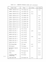
Specifications . . . • . . .
Sense Switch Settings (CPU)
Spare Parts .• . . . • . . .
· . .. .. .. .. .. .. .. .. .. . . .. .. .. . .
• •
·. ..............
1-7
2-5
4-1
v
CHAPTER 1
INTRODUCTION
1.1
GENERAL DESCRIPTION
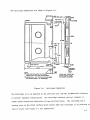
The Model 6400 Magnetic Tape Cartridge Drive (MTCD) records at 6400 bpi with a
9.2 megabyte tape cartridge.
The recording format
1S
four track serial, with a
data transfer rate in both the read and write mode of 192,000 bits per second.
integral tape cleaner is provided.
located in the CPU card cage.
.Track selection is performed by the Controller
The MTCD provides backup data storage capability
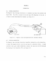
and an economical means of off-line storage of selected data (see Figure 1-1).
Figure 1-1.
An
Magnetic Tape Cartridge Drive (MTCD)
1-1
1.2
PURPOSE
This Service Manual is the primary source of information for first level maintenance.
It contains the necessary information to repair and maintain the MTCD.
This manual
contains both physical and functional descriptions, installation/operations,
maintenance procedures, and equipment supplied.
This information shall enable a Service Engineer to identify, isolate, and repair
the MTCD.
1.3
PHYSICAL DESCRIPTION
The MTCD is packaged as a single unit and is directly connected to the CPU main
frame and placed on top of the cabinet.
The MTCD is made up of a cabinet, power
supply, tape drive, and a ANSI magnetic tape cartridge.
The Cabinet contains a standard ac to dc power supply (refer to Chapter 2,
Preinstallation Checks, for 115 volts ac to 230 volts ac conversion).
A transparent
window is provided for visual inspection of the cartridge during normal operation.
The opening for the tape cartridge is directly below the window.
1.3.1
TAPE DRIVE TRANSPORT
The Tape Drive Transport, hereafter referred to as Transport, will record and
reproduce data onto and from Magnetic Tape Cartridges.
The Transport consists of
three subassemblies; Magnetic Head Assembly, Switch/Sensor Assembly, and Heat Sink
Assembly.
The Transport also contains a tape cleaner, capstan drive motor
tachometer and houses the PCBs.
1-2
1.3.1.1
Magnetic Head Assembly
The Magnetic Head Assembly consists of a closed magnetic circuit.
This circuit
IS
built of laminated high permeability metal with wound coils for inducing and
detecting flux reversals.
It is constructed as a dual gap with erase head
(read-while-write-while-erase).
Control signals are received from the Controller
located in the CPU card cage via an interface cable which enables it to write or
erase as required.
1.3.1.2
Sw.itch/Sensor Assembly
The Switch/Sensor Assembly contains circuitry to sense Beginning of Tape (BOT),
End of Tape (EOT), Load Point (LP) and Early Warning (EW).
This enables automatic
tape positioning after cartridge insertion, power on, or a rewind operation.
It
further contains the File Protect and Cartridge-In-Place switches.
1.3.1.3
Heat Sink Assembly
The Heat Sink Assembly contains the drive motor/tachometer, power transistor
circuits, and a two piece heat sink.
It is designed as a plug-in-module and
IS
center of gravity mounted.
The MTCD must be mounted in a horizontal position
only. This prevents dust and residue from falling
into the Transport which could result in lost data.
1.3.1.4
Tape Cleaner
The Tape Cleaner removes foreign material and loose oxide particles as the tape
passes the Tape Cleaner.
1-3
1.3.2
MAGNETIC TAPE CARTRIDGE
The Magnetic Tape Cartridge Assembly is shown in Figure 1-5.
Each Magnetic Tape
Cartridge Assembly is a single assembly consisting of a supply reel (to left),
take up reel (to right), a magnetic tape, file protect and belt guides.
DIRECTION OF FORWARD
TAPE MOTION
LIGHT SENSING
DRIVE MOTOR
FIXED TAPE GUIDES (2)
RUBBER COVERED
DRIVE ROLLER
TAPE PATH (OXIDE OUT)
BELT CAPSTAN
FILE PROTECT
TAPE SHOWN IN
BOT POSITION
TAKE-UP HUB
SUPPLY HUB
BELT GUIDE ROLLERS (2)
FLAT DRIVE BELT
Figure 1-5.
1-4
Cartridge Diagram
The Cartridge dimensions are shown ln Figure 1-6.
p::=q-rn SE'E NOTE 1
O.I25R
o
,0.218
6. 00
- -;.-
o
~
~ I
1.531
~2.813
I "
·~tl
(2)
:.t
-A·,
NOTE:
==~:d
-13[3
CI )FEATURES REOUIREO TO PR'EVEN!;;.tr
.
INSERTING CARTRIDGE 1P.!?ROPERlY
C2'~\lERSHALL NOT EXTEND BEYOND
(ALL Slots EXCEPT AT NOTCHESi
Figure 1-6.
BASE
TOLE.RANCE EXCEPT AS
NOTED! 0.005, LO.S"
DIMENSIONS IN ~NaiES
Cartridge Dimensions
The Cartridge is to be mounted in one position only and has asymmetrical features
to prevent improper installation.
The Cartridge contains optical elements to
enable photo-electrical detection of tape position holes.
The cartridge has a
sensing area on the front surface which senses when the cartridge is in position to
read or write (see Figure 1-7 for dimensions).
1-5
I,
MAX1MUM HEIGHT OF
FILE PROTECT PLUG
•
CARiRIOGE-IN-
I
POSITION SENSING
.
I.
J..
~l
•500
~I
. AREA
.
I
WRITE
2.140-.......~
PROHIBITED
Figure 1-7.
WRITE
PERMITTED
File Protect Switch
Tape guides are employed to guide the tape while in motion.
The file protect
cam of the cartridge is an operator rotatable switch (see Figure 1-5) which
prevents writing or erasing when in the SAFE position (see Figure 1-7).
The magnetic tape length between Load Point (LP) and Early Warning (EW) shall be
300+10-0 feet.
The tape position holes for Beginning of Tape (BOT), Load Point (LP)
Early Warning (EW), and End of Tape (EOT) are shown in Figure 1-8.
RVM
FWM
CJ·----:---:--:'~=--D
LOAD
POIN 7
t.-\RLY
WAR NIN
71t.AC.Jt!.
. LcCATIOA)S
o
o
~,0:?
~
I~"
/
/
/
~~ ___._, '/j-
r-
BOT"----AREA
3 6~ 6.0'
(i)
J-
39 II
REACHED
-
1---. [OT-
4---1
FROM Rwl) OR
.~/'i;1----.--- --- .......
RECO~D/\ELf
AREA
LOADI NG
Figure 1-8.
1-6
Tape Configuration
--J-=~ .....
'?__~
~~
The presence of a spurious tape signal, after a tape has been erased, will not
exceed 10 percent of the average base to peak read signal under test.
wound on the reel with the magnetic coating out.
The tape
1S
During forward operation it will
wind clockwise and unwind counterclockwise as viewed through the transparent door.
1.4 MTCD SPECIFICATIONS
Table 1-1 summarizes the general operation and performance of the MTCD.
This table
provides a reference source of general data for the Service Engineer.
TABLE 1-1.
SPECIFICATIONS
Parameters
Characteristics
PHYSICAL
Height
6.0 inches (15.2 cm)
Width
13.5 inches (34.3 cm)
Depth
12.0 inches (30.5 cm)
Weight
18.8 pounds (8.5 kg)
AC POWER REQUIREMENTS
Voltage
115/230 VAC
Current
1.5/.75A
Power
172 VA
Frequency
60/50 Hz, 1 phase
Heat Output
586.5 Btu/hr
DC POWER REQUIREMENTS
Voltage
+24 VDC ± 15%
-24 VDC ± 15%
+5 VDC + 5% - 3%
Current (Amperes)
+24 VDC: 1.8 typ; 3.4 max.
-24 VDC: 1.9 typ; 3.5 max.
+5 VDC: 1.4 typ; 2.6 max.
Drive Power Dissipation
18.5 Watts Typical Without Motion
57.4 Watts Typical With Motion
68.9 Watts With 10% Ramp Duty Cycle
TABLE 1-1.
SPECIFICATIONS (continued)
Parameters
Characteristics
~~'------------------------------------r--------------------------------------------------1
ENVIRONMENTAL REQUIREMENTS
Temperature
Humidity
40% to 60% RH non-condensing
Altitude
o to
10,000 feet
MAGNETIC TAPE
Read to Write Gap Spacing
.300 + .005 inch
Write to Erase Gap Spacing
.300 ± .010 inch
Write Gap to EDT/BOT Optical C/L
2.50 ± .04 inch
Erase Track Width
.032 + .005 inch
Write Track Width
.028 ± .002 inch
Read Track Width
.010 ± .002 inch
Tape Motion
Steady State
Bit Period Definitions
ANSI Standard
Speed
Range
Nominal
Speed
(ips)
Low
High
30
90
Nominal Bit Nominal Data
Period
Transfer
(microseconds)
Rate
5.208
1.74
192,000 bps
ANSI Standard #X3B5/75-43
GENERAL
Cartridge
ANSI x 3.55 - 1977 300' or 450' tape length
Recording Density
6400 bpi, MFM, or other high density codes
Recording Mode
4-Track Serial
Head Type
Dual Gap, Read-While-Write with Separate
Erase
Tape Cleaner
Integral
1-8
TABLE 1-1.
SPECIFICATIONS (continued)
Parameters
Characteristics
GENERAL
Operating Speeds
30 lpS Write, Bidirectional Read
90 lpS Bidirectional Search and Rewind
Transfer Rate
192,000 Bits/Sec.
Start/Stop Time
At 30 ips: 0.30/0.41 inches
At 90 ips: 2.97/3.42 inches
+39,:0 (Drive only, -+79,:0 cartridge inclusive)
Instantaneous Speed Variation
-
Long Term Speed Variation
-
Data Reliability
Less than 1 Error in 10 8 Bits
Interface Signal Levels
Standard TTL Levels
+29,:0 (Drive only, ±3% cartridge inclusive)
Logic 1
Logic 0
= 0.0
=
to +0.4 VDC
+2.4 to +5.0 VDC
1-9
CHAPTER 2
INSTALLATION AND OPERATION
INSTALLATION
2.1
UNPACKING/PACKING PROCEDURE
The MTCD is shipped as part of a system.
Instructions for unpacking/packing as a
part of a system are found in the system manual.
This manual will cover procedures
for the MTCD only.
2.1.1
TRANSPORT
The shipping container provides protection against moisture, dust, and contact
damage.
If the MTCD is not to be installed, but placed in storage, it should be
opened and checked for damage, then repacked.
Use the following procedure for
unpacking/packing the MTCD.
1.
Upon receipt of the shipping container, examine for damage, report any
damage to the carrier before opening.
2.
If no damage is noted, and the MTCD is not to be placed in storage, cut
the packing tape on the top center of the container and open the outer
container.
CAUTION
Use care when cutting the tapes to open the container.
Too deep of a cut may damage cabinet or transparent
door on the cabinet.
3. Cut packing tape on inner container, open container and lift out the MTCD
or Transport.
4.
Examine for damage, noting any dents, cracks, or missing parts per shippin,
list. If any are found, they should be reported to the Marketing Office
or Dealer immediately.
2-1
Use care in removing the Transport. The Heat Sink
and Pins are exposed. Mechanical damage can result
if bent or broken.
2.2
5.
All containers and packing material, especially preformed containers, must
be saved. These are to be reused if the assembly is returned to the factory.
6.
Packing is the reverse of the above procedure, using the saved container
and packing material. Add packing tape to replace the cut tape in the
unpacking procedure.
PREINSTALLATION CHECKS
The first part of this section will explain the procedure to install a Transport
in the cabinet.
2.2.1
INSTALLING A TRANSPORT
First, remove the top cover.
stick-together clamps.
In newer models, the top cover is held in place by
Remove the transparent window, then lift up on the front
of the top cover and it will snap loose.
In older models, the cover is screwed
down, remove the screws and then lift off the cover.
This will expose the inner
parts of the MTCD .
When installing the Transport, proceed as follows:
o
2-2
If unit is still plugged in:
1.
Set ON/OFF switch on rear of lower cover to OFF.
2.
Remove ac power plug from ac outlet.
o
Remove cables from PCB (Cartridge Tape Drive Power Supply) located at Jl
and J3.
o
Lift out the PCB (Cartridge Tape Drive Power Supply) and set aside.
o
Place Transport in lower cover.
VENDOR VERSION
BFC VERSION
PI
Ale
INPUT
PI
TI
1
Slit
5
II~-=-----I
ILK
6'U1
&.:..:..=:.....,.~_~ II)--':'~----I 7
2
·WH'T
~
____
~~_JII'~&-
___
~
~
I
L -_ _ _ _ _ _~~-JII;~~------~
~~-~~~~I~~-----~
.
'ro.::..--< III.......~-----"i
•.
3
r=~---+H>~~lIr~-----4
2
100
lOOV~ (~,
_005"-00(,, .. ooT
..vt
ILK
(Q~'
.005,>-001'.) -007 ~ - 0 0 8
<-008
PI
TI
I""",
v.
e'"
.t,It
I
INPUT
PI
TI
ILK
5
6fU1
6R.N
WMT
WMT
2
..,
WMT
3
WMT
•
5
•
•
~
~
7
:J
II~V.
eo
en!)
-001 .\'
II~V.
-ooa
~ INPUT
PI
ILK
-A.t
INPUT
SlK
6~N
6'U1
WHT
WMT
en!)
-001 (-oo~
2
I
I
WIoIT
/I(e CN;'MP'
2
4
'3
SWI
Z Z81 "SLle:
\
3
WKT
5
1I"" FILTe,.
LFI
TI
PI
7
~
3
•
,
7
nov. .(REF)
2
b
noV.
(RU)
-002
-o~
-002 ( -o~
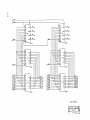
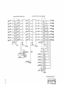
Figure 2-2.
r
Converting From lOOV to 220V
2-3
Clean heads carefully. Spray type head cleaners
are not recommended as they may contaminate the
drive motor lubricant. Cleaning the head with
hard metal objects will result in permanent head
damage.
The Tape Cleaner may be cleaned with a folded sheet of paper.
Insert the folded
paper into the open slit and move the paper up/down twice.
Install the transparent window, and insert a cartridge.
window and observe tape motion.
Look through the transparent
Tape should move forward approximately one second
and then reverse to BOT.
1.
Grasp the tape cartridge firmly with one hand and pull it from the opening.
2.
Place the tape cartridge in the opening and push forward till the stopping
point is felt and an audible sound is heard.
3.
Verify tape motion, if none; insure the ac power cord is connected, power
is on, and the fuse is not blown. If the fuse is blown or the tape still
does not move, refer to Chapter 4 of this manual.
4.
If the tape
operation.
1S
in motion and stops at BOT, the MTCD
1S
ready for normal
NOTE
If the tape was on the left reel (take-up),
automatic rewind will take place till the tape
has moved to the right reel (supply) and BOT.
2.3
SYSTEM INSTALLATION
The MTCD is part of a system, therefore the System Installation and Preinstallation
Checks are one and the same .
2-4
2.4
SYSTEM INITIALIZATION PROCEDURES
2.4.1
BASS PROGRAM
1.
Install a tape cartridge (scratch tape) in the Transport.
2.
Perform an alternate load from disc (refer to Table 2-1).
TABLE 2-1
1
Switches
2
3
SENSE SWITCH SETTINGS (CPU)
4
Function
0
0
0
0
Fixed Media Load
0
0
1
0
Fixed Media Alternate Load
1*
1*
0
1
Tape Cartridge System Load**
1
1
1
1
Tape Cartridge Alternate Load
1
0
0
1
VDT Boot
0
1
0
1
Disc Load
0
1
1
1
Disc Alternate Load
'--'
*Test SW on front panel (CPU) may be used instead of SS3
**Not allowed in present operating system.
3.
Press and release LOAD switch on processor front panel.
4.
VDT displays the PROPRIETARY MESSAGE, then:
MAKE ENTRY TO OVERRIDE DEFAULT
5.
Within 10 seconds, press carriage return (CR)
6.
VDT displays:
ENTER PROGRAM NAME
7.
Type BBIITC, then press carrlage return (CR)
8.
VDT displays:
ENTER PROGRAM NAME (*MTC OR BASS)
9.
Type BASS, then press carriage return (CR)
2-
10.
VDT displays:
BASIC FOUR ALL PURPOSE SERVICE SYSTEM
SYSTEM DATE IS: XX/XX/XX
DO YOU WANT TO CHANGE IT?
(Y/N)
11.
Type N, then press carriage return (CR)
12.
VDT displays:
SYSTEM TIME IS: XX:XX
DO YOU WANT TO CHANGE IT?
(Y/N)
13.
Type N, then press carriage return (CR)
14.
VDT displays:
1.
2.
3.
4.
B/4 SERVICE SYSTEM
INSPECTION CYCLE
BURN-IN CYCLE
DISPLAY/PRINT PREVIOUS TEST RESULTS
ENTER YOUR SELECTION (CR
= END)
15.
Type 1, then press carriage return (CR)
16.
VDT displays:
WOULD YOU LIKE TO HAVE DESCRIPTIONS OF SELECTED
BASS PROGRAMS? (Y/N):
17.
Type N, then press carriage return (CR)
18.
VDT displays a listing of all BASS tests followed by:
SELECT NUMBER(S):
19.
Type 15 (write test) or 16 (read test), then press carriage return (CR)
20.
VDT displays:
SELECTED ENTRIES: 15
ENTER ONE OF THE FOLLOWING:
R = REVIEW, CR = EXECUTE):
21.
Press carriage return (CR)
22.
VDT displays:
(A
=
ADD, D
=
DELETE,
DO YOU WANT TO LOG ERRORS TO THE ERROR FILE?
23.
2-6
Type Y, then press carriage return (CR)
(Y/N)
24.
VDT displays:
DO YOU WISH TO RESET ERROR FILE?
25.
Type Y, then press carriage return (CR)
26.
VDT displays:
(YIN):
%Mll
DESCRIPTION OF TEST
ENTER TAPE CARTRIDGE UNIT TO TEST (C0 - C3):
C~,
27.
Type
then press carriage return (CR)
28.
VDT displays:
HOW MANY ERRORS TO BE DISPLAYED ON VDT?
29.
Type 10, then carriage return (CR)
30.
At the completion of the test (approximately 10 minutes) the VDT shall
display:
DO YOU WANT TO TEST ANYMORE TAPE CARTRIDGE UNITS?
31.
(YIN):
Type N, then press carriage return (CR)
2-7
CHAPTER 3
MAINTENANCE
CORRECTIVE MAINTENANCE
3.1
3.1.1
GENERAL PHILOSOPHY
This chapter contains information which will aid the Service Engineer in
troubleshooting the MTCD.
3.2
TROUBLESHOOTING PROCEDURES
A typical sequence used to isolate the trouble to a replaceable module or PCB
1S as follows:
3.3
•
Collect information about the malfunction.
•
Examine the unit to see if power is applied.
•
Examine for a blown ac line fuse.
•
Decide if the malfunction is in the MTCD or the Controller.
•
If the MTCD is bad, switch OFF power and open the cabinet.
•
Examine for loose connectors or broken W1res.
•
Examine for broken or burned parts.
•
If the malfunction 1S located, correct it.
FUNCTIONAL DESCRIPTION
The MTCD functions within a system as a backup read and write memory device.
record mode is four track serial.
The
Data and control signals are received via an
interface (I/O) cable connecting the MTCD to the CPU.
systems of the MTCD are the Power Supply and Transport.
The two major functional
The Transport contains
two sub-functions, they are; Tape Motion Control and Read/Write Operations.
3-1
3.3.1
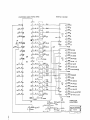
POWER SUPPLY
The Power Supply is an open frame, multi-output power supply which supplies the
Transport with its required dc voltages.
Tap changes on the Transformer (Tl) give
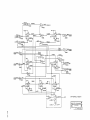
the following ranges over a frequency range of 47 to 63 hertz (see Figure 2-2).
100
110
lIS
120
+
+
±
±
10%
10%
10%
10%
200
220
230
240
VAC
VAC
VAC
VAC
±
±
±
+
10%
10%
10%
10%
VAC
VAC
VAC
VAC
The Power Supply outputs the following voltages, including a regulated S.O volts dc
±O.lV.
Measure voltage at TP4 on PCB.
Adjust RS for correct level.
±SV @ 2.6A
+24V @ 1.SA, with 3.SA surge up to 80 milliseconds
-24V @ 1.SA, with 3.SA surge up to 80 milliseconds
A crowbar overvoltage circuit is provided on the +S volts output.
The crowbar
trips above 6.5 volts dc.
3.3.2
TRANSPORT
The Transport is made up of three assemblies and five PCBs dividing the Transport
into two sub-functions.
Read/Write Operations.
3-2
The two sub-functions are; Tape Motion Control and
The assemblies and PCBs are:
Assemblies
Printed Circuit Boards
Magnetic Head
Switch/Sensor
Heat Sink
Interconnect Board
Data Circuit Board
Interface Board
Encoder/Decoder Board
Servo Board
3.3.3
SUB-FUNCTIONS OF THE TRANSPORT
A functional description of the assemblies and PCBs that make up the Transport are
best explained in the following sub-function descriptions.
3.3.3.1
Tape Motion Control
The Switch/Sensor Assembly, located on top of the drive, is used to determine the
state of the tape cartridge and the position of the tape.
The two microswitches in
the Switch/Sensor Assembly are used to originate the Cartridge-In-Place (CIP) and
File Protect (FIP) signals.
CIP goes true whenever a cartridge is completely engagE
The FIP signal will be true only when the File Protect Indicator Arrow on the
cartridge points toward the SAFE position.
This will disable the write operation.
Upper Tape Hole (UTH) and Lower Tape Hole (LTH) signals are derived from two photo
sensors.
These signals go true whenever an upper or lower tape hole has passed
the sensors.
These signals are sent directly to the Interface Board which utilizes the tape
to control tape position.
hole~
The tape cannot run forward beyond the second EOT hole
reverse past the second set of BOT holes.
3-3
OJ
3.3.3.2
Read/Write Operations
The Data Board contains a read envelope threshold detection comparator
network to assure valid read data and to discriminate against non valid
data. This network disables the Data Detected signal unless the read
envelope exceeds a certain predetermined voltage. This voltage is 60
millivolts during normal read operations; 200 millivolts during a read
after write operation (Write enable (WEN) true enables the 200 millivolts
threshold); 500 millivolts during a high speed search (High Speed (HSP-)
true enables the 500 millivolts threshold). The Read envelope threshold
detector is used to produce the Data Detected (DAD) signal.
After the selected track on the read heads have been determined, the Read
Data is input to a read amplifier, which amplifies the data to approximately
250 millivolts, and filtered by a low pass network. This MFM data, plus the
Data Detected signal, is sent to the Encoder/Decoder Board via a line driver.
The Read Data decoding stages of the Encoder/Decoder Board include a
desnake circuit (which eliminates data dropouts during periods of no
transition), a phase lock servo, a timing pulse generator (consisting of
four one-shots whose pulse widths are controlled by the servo output), and
a data acquisition circuit (which strips the preamble and a Read Data Strobe
generator.
The timing pulse generator (four one-shots) produce four sampling pulses
of variable width. Each pulse is timed by the phase lock servo to equal
one quarter of the bit cell. This division helps in the detection of the
mid bit transition which is peculiar to "one" data bits of the MFM code.
Depending on the data pattern, two of the sampling pulses (EO-A and EI-A)
which represent 0 and I data bits are applied to the data acquisition
network.
This.network develops the ~RZ ~ata. The Read Data Strobe is developed by
a fllp-flop/nand gate comblnatlon that automatically eliminates the
all-ones read preamble by disabling the Read Data Strobe during its
occurrence.
3-4
3.4
ELECTRICAL ADJUSTMENTS (For information only.
3.4.1
Not a field adjustment.)
GAIN ADJUSTMENT (DATA BOARD)
Adjust for a 1.9 volts dc positive and negative read envelope output on the lowest
output signal track using the following procedure.
1.
Using an external DEI 302030 Data Pattern Generator or its equivalent,
write an "all ones" test pattern on all tracks in MFM format. (Data
transfer rate is 192 kilohertz at 30 inches per second.) (Other data
sources may be used and none is required in drives having Codec Boards.)
2.
Read back each data track while alternately monitoring the positive or
negative read envelopes on the Interconnect Board. Test points are
J500-20 (positive envelope) and J500-3 (negative envelope) on the
Interconnect Board. Determine track exhibiting lowest amplitude read
envelopes.
3.
Adjust pot R5l3 on the Data Board for 1.9 volts dc in the read reverse
pass just after writing the track with the lowest amplitude.
4.
Recheck all data tracks. Positive and negative read envelopes of each
track should measure within ±0.05 volt dc of each other.
3.4.2
SERVO POWER ADJUSTMENT (SERVO BOARD)
Generally not required, unless a ±15 volts regulator has failed.
If failed, use the following procedure:
1.
Connect VOM or DVM reference lead to diode VR700, cathode.
2.
Attach VOM or DVM test lead to Pin 4 of operational amplifier U705.
Record -15 volts dc voltage to three figure accuracy (XX.XXX).
3.
Attach VOM or DVM test lead to Pin 7 of the operational amplifier U705.
4.
Adjust R765 until +15 volts dc is within ±5 volts in positive direction
of the reading obtained at Pin 4 of U705.
3-5
3.4.3 INTERFACE PCB ONE-SHOT PERIODS
LOCATION
PERIOD
U623 Pin 10
.9
+
.1 msec
U623 Pin 6
22
+
5 usec
U6l7 Pin 6
650
+
100 msec
U6l7 Pin 10
650
+
100 msec
U6l4 Pin 3
30
+
4 msec
U6l5 Pin 3
90
+
15 msec
3.4.4 SERVO PCB POT SETUP
3-6
1.
Adjust R76l for a voltage of 0.0 ± 0.1 volt at BALAS test point.
2.
Set forward speed with R764.
3.
Adjust R762 for a ramp time of 23 ± 0.5 milliseconds.
4.
Insure any loss of voltage that will result in loss of tape motion.
Set reverse speed with R763.
3.4.5 DATA ADJUSTMENT AND CHECK PROCEDURE
1.
Write all "ones" pattern (192 kilohertz at 30 inches per second) on track
Unit select, track 0, forward, and write enable are required.
2.
Attach scope probe to R535 on lead near R537 on board 301,061.
3.
In the Read Only Mode, adjust R5l3, refer to 301,061 until the signal
(approximately a sine wave in appearance) 1S 1.8 volts peak-to-peak.
4.
Check inter-record gap voltage amplitudes after gain adjustment. Voltage
shall not exceed 350 millivolts. All four tracks must be checked.
5.
Check DAD signal to insure true level only during data.
a.
Attach scope trigger on forward command at P3, Pin 22 of PCBA 301,094.
Observe DAD on U23, Pin 3 on PCBA 301,094. Place second (2nd) channel
lead to R535 on LEAD NEAR RS37 on PCBA 301,061 for data burst
correlation.
b.
Operate drive in READ AFTER WRITE MODE and write at least 20
consecutive data blocks for check. All four tracks must be checked.
NOTE
First 100 microseconds after Forward Command may
generate DAD spikes not of consequence.
3.5
PREVENTIVE MAINTENANCE
Preventive Maintenance which should be done by the Service Engineer is limited to
cleaning as needed, and observing safety procedures while making repairs.
Cleaning
shall be done if the Transport is replaced.
3.5.1
MAGNETIC HEAD CLEANING
The Magnetic Head should be cleaned daily if the Transport is in regular use.
Dirty heads may cause data dropouts during read and write operations.
Use a
non-residue, non-corrosive cleaning agent, such as DuPont Freon TF, and a lint
free cloth to clean the head assembly.
Be sure to wipe up any excess and allow
the heads to dry prior to operating the Transport.
3-7
Spray type head cleaners are not recommended because
overspray may contaminate the motor bearings. Also,
never clean the head with hard metal objects. This
will result in permanent head damage.
3.5.2
TAPE CLEANER CLEANING
The Tape Cleaner removes loose tape oxide and other foreign material from the tape
before it contacts the head.
This foreign material accumulates in and around the
tape cleaner and must be removed to ensure that the Tape Cleaner will continue to
work effectively.
The Tape Cleaner should be cleaned on the same schedule as the
head.
To clean, insert a folded sheet of paper in the bottom of the cleaning slot of the
cleaner.
Slide the paper up, lifting the foreign material from the cleaner.
A
soft brush may be used to remove the foreign material from the area around the tape
cleaner and head assembly.
Do not use metal objects to clean the Tape Cleaner.
If the Tape Cleaner should become scratched, it
could scratch the tape surface, resulting in lost data.
3.5.3 MOTOR CAPSTAN CLEANING
The Capstan is composed of hard polyurethane and must be cleaned after foreign
material has built up.
Clean, using Freon and a lint free cloth.
schedule should be the same as for the head.
Be careful not to permit cleaning solvent to drip
into the drive motor bearings as it will result in
a failed component.
3-8
The cleaning
CHAPTER 4
REMOVAL/REPLACEMENT PROCEDURE
4.1
SPARE PARTS LIST
TABLE 4-1.
4.2
SPARE PARTS
BFC MM
Vendor
160189
MDX-04.000
FUSE, 4A-MDX SB
5
160190
MDA-12.000
FUSE, 12A MDA
5
610010
B903030
PCB, CART TAPE CONTROLLER
1
610020
NB903040
PCB, CART TAPE POWER SUPPLY
1
610710
900960-002
CABLE, CARTRIDGE TAPE
1
611000
902761-001
TAPE DRIVE TRANSPORT
1
617010
345002
FAN, COOLING
1
617020
100321
SWITCH, TOGGLE
1
617030
180007-001
TRANSFORMER
0
737020
181003
RFI, FILTER
1
Description
Quantity
REMOVAL/REPLACEMENT PROCEDURE
This section explains the procedure to remove the major (spared) assemblies and
install their replacements.
Before removing any assembly, the following steps
shall be followed:
•
Remove Magnetic Cartridge
•
Set power switch to OFF position
•
Unplug the ac power cord from its source
4-1
4.2.1
PCB CARTRIDGE TRANSPORT POWER SUPPLY
This PCB is removed in the following manner:
•
Complete steps in Section 4.2.
•
Lift off the top cover of the ~rrCD (older models have screws holding them
in place of the (3M) stick-tight connections). These screws must be
removed to remove the top cover.
•
•
Locate the PCB.
•
•
Disconnect the cable at Jl.
Lift up on the PCB till the connectors J2 and J3 can be seen.
Disconnect the cables at J2 and J3.
•
Remove the PCB.
•
To install a new PCB, repeat the above in reverse order.
•
Verify the regulated +5 volts is within tolerance (refer to Section 3.3.1).
4.2.2
TRANSPORT
To remove the Transport, first complete the steps ln Section 4.2, then do the
following procedure.
•
Remove the screws located on the bottom of the MTCD.
•
Lift off the top cover.
•
Disconnect the PCB Cartridge Tape Drive power supply and remove per
Section 4.2.1.
•
Lift the Transport up and to your left, placing on right side of MTCD.
•
Disconnect cable at P702 of Servo PCB.
•
Disconnect the I/O cable at P3 of Encoder/Decoder PCB.
•
Lift the Transport up and set to one side.
•
To install the Transport repeat the above in reverse order, connecting
cables as required. Place top cover in place and tighten all screws
loosened or removed.
,
4-2
CHAPTER 5
REFERENCE DATA
5.1
PURPOSE
This section contains Logic Diagrams, Schematics, and drawings used in the MTCD
and is intended to be used ONLY by Service Engineers as a troubleshooting aid.
5-1
Tape Motion
Description
Name
Signal
FWD-
Forward
When troe. causes the tape to move in a forward direction.
REV-
Reverse
When true. causes the tape to move in a reverse direction.
HSP-
High Speed
When true, causes the tape to move at high speed in the direction
selected by either FWD- or REVTape motion will proceed until the command signals go false or:
RWD-
a.
In forward where an EOT hole is en counted whereupon motion
will stop.
b.
In reverse where a set of BOT holes is encountered whereupon
motion wlll stop.
c.
Both directions are commanded Simultaneously whereupOn the
tape wlll stop.
d.
Rewind command is received which will overrule other motion
commands.
e.
Internal Ready signal is not troe whereupon motion will stop.
f.
In High Speed. motion will drop to low speed when the upper
"load point" hole is sensed in reverse or the upper "early
warning".. hole is sensed in forward .
When true. causes the tape to be positioned to beginning of tape at
high speed. The Tape Drive must be selected to start a Rewind
sequence. but may be unselected after the sequence is started.
Rewind
Beginning of tape is defined as between the two innermost (toward
the Qliddle of the tape) set of upper and lower holes located at the
"head end" of the tape. This location is r~commended for unloading
the cartridge as the data recording a'rea is completely protected.
Rewind will "overrule" all other motion signals. Successive
Rewind commands will not cause the tape to be "run off".
Rewind will stop if the internal Ready signal is false.
An automatic Rewind sequence is executed when a cartridge is
installed in the Tape Drive or when. power is applied when a
cartridge is installed.
Input Data
Signal
Name
WEN-
Wrlte Enable
WDA-/
WDA+
Wrlte Data
Delcrlptlon
,
When tnae. enable I the writing and eraBlng functions for the lelected
track. The wrlting and eraling proce8lel occur only if the cartrldge
I. In the unprotected .tate (not lafe). Thil Ilgnal il internally latched
aDd 91111 remain .et unlell relet by:
-Revene or Hlgh Speed commands
-Internal Ready Ilgnal, not true.
W111 modulate the wrlte head to produce a recorded waveform on
tape when WEN- II true and the cartridge is In the unprotected
state (not .afe).
In WDA+ (unactuated) ltate, the tape wlll be erased in the ANSI
!alhion. The WDA- ltate 91111 cause the opPosite polarity to be recorded. Therefore. if no erase head is used, eraSing can be done
by usmg the write head.
5-2
The minimum clock period for data input Ihould not allow the resultant number of flux reversal from exceeding 3200 per lnch
(1260 nux reverBal/cm) and the rile and fall times should not be
creater than 0.5 microseconds.
Output Status Signal s
Signal
Name
Description
SLD-
Drive Selected
Will be true when the Tape Drive has received its proper unit
address.
RDY-
Drive Ready
Will be true when a cartridge is installed, the sensor lamp is drawing current, and the +5 VDC is applied to the Tape Drive.
BSY-
Drive Busy
Will be true when the Tape Drive is in an automatic rewind sequence
(I.e. when a cartridge is first installed in the Tape Drive), or when
the Tape Drive is executing a rewind, forward, or reverse command.
This signal will go true when the command is received and will remain true until the motion has stopped (i. e. 30 milliseconds after
low speed motion has been commanded to stop and 80 milliseconds
after 90 ips operation has been commanded to stop).
In the case of receipt of a non-executed or illegal command, (FWD
at EOT or REV at BOT), this signal will not be true, iDdicating the
command is rejected.
FW-
Flag
Will be set and latched when an automatic sequence to position the
cartridge to BOT has been executed, or a rewind has been completed. This signal is reset by subsequent receipt of a FWD command.
WND-
Write Enabled
Will be true when a write enable condition is latched withln the
Tape Drive.
FUP-
File Unprotected
Will be true when a cartridge is installed and it is in the unprotected
state (1. e. can be written on).
LPS-
lpad Point Sensed
Will be set and latched when the upper load point hole (the warning
of beginning of tape) is passed in the reverse direction. This signal
will be inte~lly reset when the load point hole is subsequently
passed in the forward direction. When this signal is true, high
speed will be disabled. Reverse tape motion is allowed to proceed
until the BOT holes are encountered where the Tape Drive will stop
and accept only forward commands.
EWS-
Early Warning Sensed
Win be set and latched when the upper early warning hole (the
warning at end of tape) is passed in the forward direction. This
signal will be Internally reset when the early warning holes is subsequently passed in the reverse direction. When this signal is true,
high speed is disabled. Forward tape motion is allowed to proceed
until the EOT hole is encountered where the Tape Drive will stop
and accept only reverse commands.
Output Data •
Signal
RDA
Name
Read Data
Description
This lignal is a repUca of the WDA data written onto the tape. The
RDA line is latched and its initlal state is Dot preset, thus, initlally
the RDA line may be high or low. Conditions can occur wherein single
transitions can occur during erased portion.&.. 9f the tape. These can
set the RDA line in the opposite state.
The read signal is always available in dual gap drives, and is always
avallable when WEN has been set for single gap drives.
The threshold levels are internally set as a function of the mode of
operation.
· NOT ETape- Drives with Encoder/Decoder circuit
board assemblies have interface signals the same as
serial Tape Drives equipped with interface circuit
board assemblies. except the WDA and RDA signals
Input Data For Drives With an Encoder/Decoder Circuit Board Assembly
Signal
WDE-
Description
Name
Write Data Enable
A control line to the Tape Drive which separately allows enabling
of the write function (the sending of write data strobes and the
writing of data on tape). The \\'EN function is still required and
will enable both writing and eraSing. WEN causes the write
circuits to become active and tape to be erased. after the tape
is up to speed and other conditions met, the WDE will cause the
Tape Drive to send the first data strobe and shall commence to
record flux transitions on the tape.
A 11 data which is to be written on the tape must be sent to the
Tape Drive (all preambles. postambles. and check characters)
and that data is recorded in Manchester form, phase encoded.
\\,NZ-
Write Non-Return Zero
Data
During the write data strobe period the state of the input write
data line is sensed as follows:
WNZ
WNZ
= Low = 1.
~
and
High = 0
The state of WNZ is only examined during the write data strobe
period. The WNZ signal must be steady 0.5 ",sec prior to the
the Write data strobe true period (WDS = Low).
Table 3-10. Ouput Data For Drives With an Encoder/Decoder Circuit Board Assembly
Description
Signal
Name
DAD-
Data Detected
Wlli be false except when data has been detected. Data detected
requires the receipt of at least 12 zeros and a one following without
a period of 2.5 bit times without data being received. Data detected
can be used to sense the presence of the block of data. This signal
will strip the preamble from the read data signal and is used to
enable the other data output signals.
RNZ-
Read Non-Return to
Zero Data
During read data strobe period if RNZ is low (true) then the data is
a one, if high then the data is zero.
RDS-
Read Data Strobe
Will be low for 0.3 :1:50% ",sec indicating that RNZ can be sampled
during this period.
Read data in the forward direction will have preamble removed and
will stay true for all of the postamble and for approximately 2.5 bit
times after postamble has passed. (Therefore, CRCC and postamble
must be stripped in forward direction and the CRCe and preamble
must be removed in the reverse direction.) To first set read data,
12 zeros must be sensed. A drop-out will shut off circuit if it exists
for>2.5 bit times (50 ",sec) am circuit will stay off for 13 bit times
(~290 ",sec).
The read data threshold levels are internally set to three different
levels depending on the write and motion commands. Read only
threshold or-curs when running at low speed without writing. Write
threshold OCl-un when writing. Search threshold occurs when running
at high speed.
WDS-
5-4
Write Data Strobe
The write data strobe is generated within the encoder/decoder module
and is sent out to indicate when the Tape Drive is taking data. The
low or true strobe period is 5.2 :1:5% ",sec.
APPENDIX A
MAGNETIC TAPE CARTRIDGE CONTROLLER
TABLE OF CONTENTS
Page
APPENDIX A
MAGNETIC TAPE CARTRIDGE CONTROLLER
SECTION I
INTRODUCTION
AI.I
AI.2
AI.2.1
AI.2.1.1
AI.2.1.2
AI.3
AI.3.1
AI.4
General Description . . .
Physical Description . .
Firmware Description .
Control Structure . .
Command Sequencing .
Physical Requirements . .
General Specifications
. · . . . . . . . ..
..
. · . . . . . . . ..
..
. · . . . ..
......
.
. ..
.....
. . . .
.
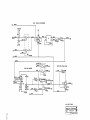
...
. . .
. . . . . .
Options . . . . . . . . . . . . . . . .
..
SECTION 2
INSTALLATION
A2.1
General Description . . . . . . . . . . . . . . . . . . . . A2-1
SECTION 3
MAINTENANCE
A3.1
A3.1.1
A3.1.2
A3.1.3
A3.2
General Description . . . . . .
............
Microprocessor Logic
. . ..
........
Computer Interface Logic
. . . . . . . . . . . . . .
Magnetic Tape (MTCD) Interface Logic . . . .
. .
Functional Parameters . . . . . . . . .
. . . .
SECTION 4
RECOMMENDED SPARE PARTS/GLOSSARY
A4.1
A4.2
Recommended Spare Parts List . . . . . . . . . . . . . . . A4-1
Glossary of Mnemonics . . . . . . . . . . .
. A4-1
. ..
SECTION S
REFERENCE DATA
AS.I
Reference Data
.
.
.
.
.
.
.
.
.
.
.
.
.
.
A1-1
A1-1
A1- 7
Al- 7
AI-8
AI-IO
AI-IO
AI-12
A3-1
A3-2
A3-4
A3-S
A3-6
. . . . . . . . . . . . . . . . . . . . . . AS-I
iii
LIST OF ILLUSTRATIONS
Page
Figure
Al-l
Al-2
A3-1
Magnetic Tape Cartridge/Controller Interface Cabling
. AI-I
Controller PCB . . . . . . . . . . . . . . . . . . . . . . AI-2
Cartridge Tape Controller Block Diagram. . . . . . . . . . A3-1
LIST OF TABLES
Table
Al-I
AI-2
Al-3
A4-1
iv
Tape Unit Interface Signal List
...
. .
Computer Interface Signal List . . . .
. . .
General Specifications
...... .
. .
Spare Parts . . . . . . . . . . . . . . . . . . .
. . .. . . AI- 3
. ..
AI-4
. . . . . AI-II
. . .
. . A.4-1
SECTION I
INTRODUCTION
AI.I
GENERAL DESCRIPTION
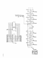
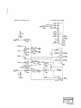
The Magnetic Tape Cartridge Controller is a standard size Basic Four printed circu:
board (PCB).
This PCB is located in the card cage (CPU Backplane) of the CPU.
Fo:
a typical system interconnection diagram, see Figure AI-I.
900960-002
TAPE
CNTRL
~-.r-I903030
TAPE DRIVE
Figure AI-I.
AI.2
CPU CARD CAGE
Magnetic Tape Cartridge/Controller Interface Cabling
PHYSICAL DESCRIPTION
The Magnetic Tape Cartridge Controller, hereafter referred to as the Controller, i:
a single PCB plugged directly into the card cage of a processor system.
A single
interface cable (part number 900960-002) connects the Tape Drive and CPU Backplane
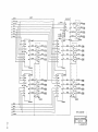
For drawing of the Controller PCB, see Figure AI-2.
Al-l
",.
'.'
4':"C'~t
z.-y liIAP''j'':'''' k~':,.!., :;;-:;;-:-R.tl ",,~;;:_ -,-;-;:' :
I;;~{~~;;;-~~- -=~m
tt.l '.'
,1'..-".1: l~·.'J;'; -;re".t ,.~~~---,•.
;fWll , : :' "JI
1-'
"fI_~
.~_~.~i~l~~:.~,.~r!~_~··E£E~~~~__
r.
.:5
07
7"
,-.'( I~-
.
'(7lJ'.J~ ,
WJ75 1&5«.JI, - Ii" 7
ft_'!,! CH.d"""''''; ,-9'", ~~ ,
15-/
~2
~"'S
..
Tt··
/l'/o ... <f·
REwr.R< C-V 8,0·-
-
_
-.-,
yO?'" S"'i'
B-2
...
..,
ADO': D Ie -'91'" 5"8
C#AN6ED Ie'S"
Ar
D, 4€~ t.~ f'It!,
:z
REwORk. "",81>S.
90~{)~;f'10~o:>9
C20~C35
C:X:7
B8
1
BC
~
GO
DO
(}D
[KJ
CKJ CKJI
~36
P2
1
80
{
8E
n
<::)CIO
001
LiU DL3 I
CJC40
{\
I 1:5
1'<.>
,-,
LJO
I
-'
f1
9H
{I
8H
.
-c:>-~C41
{j
-cJ-1
]I
R'
I
9L
c4Q-
<I
8L
~C27
7E
~
~C38
7F:J
IC
7H
~
C:::>C14
C::>C31
[]D
n
~28
~C25
C:::>C15
OIJ ~ CKJ [201
I
DU UL3
]
OEJ
~I
7L
J
I
[IJ
gpk
~
3J
1I
PI-
IG
i
<:JC17
CEJI
IH
(
<:Jcle
{I
2J
II
~C23
R9I=
I
2L
{I
=C24
IJ
(
C:::>Ct9
I
CK3
~~in
C50-
2G
-c:>-
QZJ
CEJ CEJ
~I
DE] ~
CJC34
71<
3G
<
C:::>C16
~C26
=C29
J
IF
~C22
=C33
7J
i
CK3 OK] OIJ GO 00 [JD
c::>C32
7G
l-
IK
i
C:::>C20
IL
-
i
C60-
tNI..c:/""'" II:DIDQlMKM' ~
DlIH .... I~ "". ttl IICHIt
'OllUNCIl
... I.'
.......
,.,..,
I _ ....... C.......
I,IIIU. OTM' ............ CI ... D
IMCttI"'D~
NUT ASS'"
Figure Al-2.
Controller PCB
USED ON
....
tI.
i-n"~~
~o_ fLl~
~
0'1_"'•
MCM.. . .
Al-2
JW!t- It
50-"2- L~
C:::>C13
~C37
~C39
8J
lJ
I?EV 'YL !.TEM
C:X:12
~30
R2
no'"
~..,I(
~c.'"
I..;';>f) ... -rc.)
m=J CJ:[J
O£J O[J [}£] QU OU Q[J
C:X:9
~I
C:::>CII
ITO rn:J,.
<
(
~C21
QU
C:::>CB
I
0
~E'~
("~rs
c3O-
QD c::2Q CE3 [EJ ~ ~ 00 QD
I
r'--
~t..zs
,
~,o.
D
C
/I'
r
DO NOl SCAlf OU,WI,.O
M'
.,..
p.
•
·.r
~~
!..d..:J
.1.'1,.
1.:,-, '"
~
.......~.~_
""'~CB
A
CARTR(
TAPE CONT
'0 r··' 903030
I"'''' ,., I... '
,
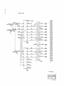
The Tape Unit Interface Signal List
TABLE AI-I.
1S
contained in Table AI-I.
TAPE UNIT INTERFACE SIGNAL LIST
Pin
Signal
22
SLD-
Drive
Selected
4
RDY-
Drive
Ready
6
WND-
Drive
Write Enabled
8
FLG-
Drive
Flag
10
LPS-
Drive
Load Point Sensed
12
FUP-
Drive
File
14
BSY-
Drive
Busy
16
EWS-
Drive
Early Warning Sensed
18
RWD-
Controller
Rewind
20
REV-
Controller
Reverse
22
FWD-
Controller
Forward
24
HSP-
Controller
High Speed
26
WEN-
Controller
Write Enable
28
SLl-
Controller
Unit Select 2
30
SL2-
Controller
Unit Select 21
32
SL4-
Controller
Unit Select 22
34
SLG-
Controller
Select Gate
36
RNZ-
Drive
Read NRZ Data
38
RDS-
Drive
Read Data Strobe
40
DAD-
Drive
Data Selected
42
WDE-
Controller
Write Data Enabled
44
WNZ-
Controller
Write NRZ Data
46
TR2-
Controller
Track Select 2
48
WDS-
Drive
Write Data Strobe
50
TRl-
Controller
0
Track Select 2
From
Conunents
Unprotect~d
0
1
The MTCD pin-to-pin listing of the interface cable is shown in Figure 2-4.
Al-3
The Computer Interface Signal List 1S contained 1n Table
TABLE
Al~2.
Signal Name
Al-4
Al~2.
COMPUTER INTERFACE SIGNAL LIST
Type
A Pin
B Pin
B-44
Master Reset
TTL Input
A-6
Clock Phase 1
TTL Input
A-6
Clock Phase 2
TTL Input
B-22
I/O Control Reg 1
TTL Input
B-3l
I/O
Reg 2
TTL Input
I/O Control Reg 3
TTL Input
B-6l
Output Data Bit 0
TTL Output Bus
B-39
Output Data Bit 1
TTL Output Bus
B-lO
Output Data Bit 2
TTL Output Bus
Output Data Bit 3
TTL Output Bus
B-58
Output Data Bit 4
TTL Output Bus
B-37
Output Data Bit 5
TTL Output Bus
Output Data Bit 6
TTL Output Bus
Output Data Bit 7
TTL Output Bus
Input Data Bit 0
TTL Input Bus
Input Dat'a Bit 1
TTL Input Bus
Input Data Bit 2
TTL Input Bus
Input Data Bit 3
TTL Input Bus
A-62
Input Data Bit 4
TTL Input Bus
A-32
Input Data Bit,S
TTL Input Bus
Input Data Bit 6
TTL Input Bus
Input Data Bit 7
TTL Input Bus
B-60
Priority In
TTL Input
B-54
Priority Out
TTL Output
Contro,~"
A-3l
A-26
I
A-lO
I
B-26
A-58
B-32
A-60
B-62
B-59
A-6l
A-55
TABLE Al-2.
COMPUTER INTERFACE SIGNAL LIST (continued)
Signal Name
Type
A Pin
Select In
TTL Input
Select Out
TTL Output
A-52
External Interrupt
Request
TTL Output
A-38
+5 Volts DC
Power
B Pin
B-52
B-1
B-2
B-64
B-65
Ground
Return
A-I
B-19
A-2
B-35
A-13
B-36
A-14
B-56
A-18
A-33
A-34
A-56
A-64
A-65
Memory Address Bit a
TTL Output Bus
B-5l
Memory Address Bit 1
TTL Output Bus
B-53
Memory Address Bit 2
TTL Output Bus
B-55
Memory Address Bit 3
TTL Output Bus
A-50
Memory Address Bit 4
TTL Output Bus
A-53
Memory Address Bit 5
TTL Output Bus
A-54
Memory Address Bit 6
TTL Output Bus
A-IS
Memory Address Bit 7
TTL Output Bus
A-9
Al-~
TABLE AI-2.
COMPUTER INTERFACE SIGNAL LIST (continued)
Signal Name
Type
A Pin
B Pin
;
Al-6
Memory Address Bit 8
TTL Output Bus
Memory Address Bit 9
TTL Output Bus
A-II
Memory Address Bit 10
TTL Output Bus
A-12
Memory Address Bit 11
TTL Output Bus
B-13
Memory Address Bit 12
TTL Output Bus
B-7
Memory Address Bit 13
TTL Output Bus
B-18
Memory Address Bit 14
TTL Output Bus
B-9
Memory Address Bit 15
TTL Output Bus
B-47
Memory Address Bit 16
TTL Output Bus
B-33
Memory Address Bit 17
TTL Output Bus
B-4l
Memory Data Bit 0
TTL I/O Bus
B-34
Memory Data Bit 1
TTL I/O Bus
Memory Data Bit 2
TTL I/O Bus
B-43
Memory Data Bit 3
TTL I/O Bus
B-28
Memory Data Bit 4
TTL I/O Bus
Memory Data Bit 5
TTL I/O Bus
B-30
Memory Data Bit 6
TTL I/d Bus
B-40
Memory Data Bit 7
TTL I/O Bus
B-27
DMA Acknowledge
TTL Input
A-57
DMA Request
TTL Output
A-44
DMA Memory Address
Bit 15
TTL Output Bus
B-57
Read Enable
TTL Output Bus
B-23
RTXX-
TTL Input
B-20
Transmitted DMA
Acknowledge
TTL Output
B-48
High Speed DMA
TTL Output Bus
B-14
A-35
A-36
A-24
Al.2.l
FIRMWARE DESCRIPTION
The firmware is divided into two portions:
1.
The Control Structure - includes power-on-sequencing, initialization,
"Executive" idle loop and all paths in and out of the "Executive".
2.
Command Sequencing - routine which realizes the Controller commands.
Al.2.l.l
•
Control Structure
INIT - this routine begins at address 000 6' A Controller Reset (caused by
I/O bus signal RESET - being asserted or ~y software issuing a Reset Control
operation) forces firmware to begin executing at INIT as soon as the reset
condition is removed. INIT performs the Controller Initialization.
First, Controller status is set to FF, then all used ROM locations are
added together (Modulo 256) and compared with an expected sum stored in
ROM location KSUM. If the two sums are the same, then the Read/Write
memory is tested. Each memory location is tested to verify that the
following patterns can be written and read from it: 00, FF, AA, 55, and
XY (XY is the 8 LSB of the memory location's address). If these tests
also succeed, the firmware sets the Controller status to 00 and proceeds
to START.
•
START - various Read/Write Memory locations are set to O. The Z80 interrupt
mode is set to 1. The Z80 stack pointer is set to CFF
(the top of Read/
16
Write Memory). The Z80 HI register pair is cleared ana the "Executive"
idle loop, EXEC, is entered.
•
EXEC - this routine provides the main control structure of the operational
firmware. When entered via "START", EXEC has nothing to do, so it loops
(testing several internal and external flags) looking for things to do.
One flag may be set by the Controller's I/O bus hardware, Command Received.
(This flag is included as bits 5 of Input Port 27 ,) Two internally-create l
16
situations, caused by previously issued commands, are also tested as follows
1.
When processing a Rewind command, the firmware merely initiates the
Rewind, sets an internal flag to indicate the unit is rewinding and
returns to EXEC (up to four units may be rewinding simultaneously).
EXEC, then, will test the status of a rewinding unit until it reaches
Beginning of Tape (BOT), at which point an interrupt will be initiated
for that unit.
2.
Most Controller interrupts are processed through subroutine "SUINT".
As described in the discussion of that routine, interrupts may be
disabled by the executing software. If so, the Controller firmware
will set a flag indicating an interrupt is "queued" and will return
to EXEC. EXEC will monitor the two interrupt enable flags (Attention
and Command Complete, bits 6 and 7 of Input Port 27 16 ), When an
interrupt is re-enabled and a corresponding interrupt is queued, EXEC
"unqueues" the interrupt and branches to "SEXIN" which performs the
interrupt of the CPU.
Al-7
•
ECMDD - when a command is received, EXEC branches to this routine. This
routine first sets the Controller's main status to "Busy" (by writing an
8016 to Output Port 2016)' then reads the command byte from Input Port 2016'
The four most significant bits (comprising the CMD field) are then used to
branch, thru a table, to the routine which is coded to perform that command.
•
SQINT - this subroutine is called by most routines at the completion of
their normal operation or to abnormally abort a command. Two types of
interrupts are defined in the product speCification, Attention and Command
Complete (which are essentially non-data-transfer and data-trans fer-interrupt
Each may be selectively enabled or disabled by software. For each interrupt
request, SQINT tests the associated enable/disable bit in Input Port 27
16
(bit 6 for Attention, bit 7 for Command Complete). If enable, control 1S
passed to "SEXIN". If disabled, an interrupt of the appropriate type is
queued and control is returned to the calling routing.
•
SEXIN - this subroutine, updates the Main and Auxiliary status bytes (and
makes the Controller "Not Busy"). The interrupt requests flip-flop input
to the CPU, it is then set by simply writing to Output Port 25 , and is
16
reset by the CPU acknowledging the interrupt. Control is then returned to
the calling routine.
•
EIPL, EIPLI - these routines initiate and control the firmware sequencing
through the IPL sequence.
Al.2.l.2
Command Sequencing
Non-Data-Transfer Commands
The following routines are used to perform the set of non-data-transfer commands
defined for the Controller.
They include certain subroutines which deal with the tape unit control and status
lines.
These routines are used by most of the major command-performing firmware
routines.
Al-8
•
EILL - an illegal command status is posted, then control is passed to SQINT.
•
ECLRI - any queued interrupts are removed from the queues. The status of
the tape unit whose number is coded in the command is placed into the main
and auxiliary status bytes. The Controller is made "Not Busy", and control
is passed to EXEC.
•
EREW - (Rewind). The last used track for the desired track is selected,
then the unit's status is tested. If the unit is not ready, an abnormal
termination exit is taken. Otherwise, the Rewind line to the unit is
pulsed and control is returned to EXEC.
•
EUNLD - (Unload). Similar to Rewind, except that the tape unit "Unload"
control line is raised until the unit reaches End of Tape (EaT) (which 1S
signified by the unit becoming "Not Busy"). Control is then passed to sQn
•
ESP - all space commands cause control to be passed to this routine (Space
File and Record, Forward and Reverse). Subroutines SELU and SREADY are
called to select the unit and verify it is selected and ready. SBOT is
called to check for reverse motion requested with tape positioned at BOT.
Then routine SMOT is called to initiate tape motion. When tape is up to
speed, subroutine SDAD is called to wait until data from tape is detected
(i.e., the start of a record). Then, depending on forward or reverse
motion, ESPFWD or ESPREV is entered. These routines read the first data
bytes from tape and test for a value of 0. If 0, the record is a "File
Mark". Control is passed to EFM where tape motion is stopped, a File Mark
status is posted, and control is passed to SQINT.
If not a File Mark, control is passed to ESPI to wait for the record to pas
If the command is a Forward File or Reverse File command, then the firmware
loops to space over the next record until a File Mark is reached.
If a Forward Record or Reverse Record command, tape motion is stopped,
normal status is posted, and control is passed to SQINT.
Data Transfer Commands
The following routines perform the read, write, and data test command set of the
Controller.
•
EWRT - (Write, Write Gap, Write File Mark). All write-oriented commands
enter this routine. Write Gap and Write File Mark proceed similarly to the
space commands (see ESP above), except that: (1) the Tape Unit's Write Enab:
line is activated prior to initiating tape motion, (2) the INIT flip-flop
is toggled to r'eset the write bit counter and various control terms in the
tape unit interface logic and, (3) the last flip-flop is set in preparation
for initializing the write CRC generation chip. Then, based on the command
code, either EWG or EWRT2 is entered.
EWG (Write Gap) - this routine simply delays enough time for about 4
inches of tape to be erased. Tape is stopped, their SQINT is called.
EWRT2 (Write File Mark) - see the discussion of this routine below for
the Write command.
For Write Data, start up is different. The firmware must fetch the control
block from main-frame memory (using subroutine "SGETCB") to establish the
number of bytes to write and where the data buffer is in memory. Tape
motion is then initiated ("SMOT") and control is passed to "EWRT2".
•
EWRT2 (Write) - the write function can be broken down into three main
portions: (1) front of record, (2) body of record, and (3) end of record.
Front - this portion of firmware must write the preamble, initialize the CRe
generator, and write the Leader on tape.
•
ERSS, ETST, ERD - after write, these are anticlimactic.
Al-9
Subroutines
These routines are llsed by many of the above described routines.
•
SELU, SELUA - sets the track and unit numbers on the tape unit interfaces,
tllen asserts the select line, thereby "selecting" the desired unit.
•
SELUA - selects the track last used on the unit.
•
SELU - selects the track specified in the command.
•
SREADY - tests that the selected unit is selected, "Ready", and not Rewinding.
If not, a not ready exit is taken, posting an abnormal condition status and
calling SQINT.
•
SGETCB - fetches the 7 byte control block (CB) from main memory by reading
addresses 7016 - 76 16 . It then places. the address portio~s of the CB ~n
the DMA Address Reglster and returns wlth the byte count ln the DE reglster
pair, the 16 address LSBs in the HL pair and the Index bytes in Read/Write
Memory.
•
SMOT - starts tape motion, providing appropriate delays to ensure proper gap
size and proper head positioning before tape is written or read. SMOT tests
for forward or reverse tape motion, setting the appropriate control signal
to the selected tape unit. After SMOT commands the units to Move, it
samples the units BSY (busy) status to insure it goes busy - if not, tape
is either at physical EDT (forward motion) or BOT (reverse motion). If this
occurs, control is not returned to the calling routine, instead the status
is updated to reflect an "error" exit to "IERR3A".
•
SDAD - this routine simply tests the tape units Data Detected (DAD) which
is connected as bit 1.
•
SBOT - test for BOT. This routine aborts reverse motion commands issued
to a unit positioned at BOT and insures that the Load Point area of the
Tape is not used by any of the forward commands.
Al.3
PHYSICAL REQUIREMENTS
The Controller will be installed in the card cage of a standard Basic Four data
processing system.
All clearance and airflow provisions normal to the Basic Four
system will be observed.
Al.3.l
GENERAL SPECIFICATIONS
The general specifications including Electrical, Interface, and Environmental are
listed in Table Al-3.
AI-IO
TABLE AI-3.
GENERAL SPECIFICATIONS
Parameters
Characteristics
ELECTRICAL REQUIREMENTS
DC Voltage
+5 V + .25 V
DC Current
3.8A
INTERFACE REQUIREMENTS
Signal Levels
(Standard TTL)
0.0 to +0.4 V equals logic low
+2.4 to Vce equals logic high
Termination
All lines exceeding 2 feet will
terminate with 220 ohm pull up
resistors and 333 ohm pull down
resistors
ENVIRONMENTAL REQUIREMENTS
Operating Temperature
Operating Humidity
40% to 60% non-condensation
Operating Elevation
-500 to 7,000 feet above sea level
Storage and Shipping Altitude
-500 to 30,000 feet above sea level
AI-II
Al.4
OPTIONS
(This Page Left Intentionally Blank)
Al-12
SECTION 2
INSTALLATION
A2.l
GENERAL DESCRIPTION
The installation procedures are explained in the System Manual and the MTCD
installation.
They are therefore not repeated here.
A2-1
(This Page Left Intentionally Blank)
SECTION 3
MAINTENANCE
A3.1
GENERAL DESCRIPTION
Maintenance of the Controller is limited to replacement of the Controller itself.
This section will explain the Controller function only as an aid to the Service
Engineer in troubleshooting.
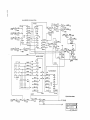
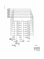
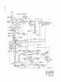
A Functional Block Diagram 1S shown 1n Figure A3-1.
.....
~L
"
,
.
n,,.1!
...
"""T
z.,"It.'..~e
IH'Cll.f>'.Uc!E5J'~
I- "6-1(.
Figure A3-1.
Cartridge Tape Controller Block Diagram
A3-1
The Controller is a complete link between the computer program and the tape unit.
The Controller performs command decoding, tape start/stop timing generation, tape
record formatting, tape position, status reporting, and interrupt control.
As such,
it is a combination of Controller/Formatter.
The Controller is designed around a Z80 MOS Microprocessor.
The three major
functional (logic) blocks begin with the microprocessor logic.
A3.l.l
MICROPROCESSOR LOGIC
Memory addressing and I/O ranges are limited by design to be sufficient for use in
this environment.
The Microcomputer is comprised of the Z80, clock generator,
buffers for Z80 address, and control line, memory bank, and I/O decoders.
The clock circuit divides the 5 megahertz CPU clock CPH2- by two, creating a
2.5 megahertz square wave clock.
functions on the board.
This clock is driven to most other clocked
The buffers increase the drive capability of the Z80
outputs to drive the multiple TTL loads on the Controller.
The memory bank
decoder 6L translates Z80 address bits 9, 10, and 11 into eight 512 byte bank select
lines.
Since address lines 12 thru 15 are not connected, the memory address space
consists of 4 kilobytes.
By convention, the firmware for the Controller places
this 4 kilobyte space in addresses 0000
16
thru OCFF
16
.
The address decoder is
enabled by the Z80 MREQ signal, creating unique "chip enable" outputs from the
decoder.
Tpese select lines are directly connected to PROM and RAM chip enable pins.
The two I/O decoders (6D, 8F) are similar in their implementation.
by the Z80
10 and address bit 5. They are selectively enabled by the WR (write)
and RD (read) control lines.
address bit 5
1S
They decode the three LSB address lines.
an enable, the decoders are active for
XXIXXyyy where X can be 0 or 1 and yyy is a 3 bit code.
A3-2
Both are enabled
Because
10 ports with addresses
So, for each yyy there are XXXX (16) possible occurrences.
By firmware conventions
the XXXX is always set to 0000, so the I/O decoders actually decode ports 2016 thru
27
16
Due to the timing relationship of the address lines and the 10-, RD-, and WR
.
control lines, the decoder outputs are "glitch-free" pulses.
This is important as
it allows the decoder outputs to be directly connected to the flip-flop clock and
clear pins.
The Read/Write Memory's (RWM) and Read Only Memory's are 256 x 4 bit and 512 x 8 biparts, respectively.
The two RWM chips are enabled together to provide a 256 byte
Read/Write Memory array (Note that 246 bytes of the "space" enable by MBK6- are
unused).
Each prom chip is uniquely enabled by one memory decode signal.
The
Controller has sockets for 6 ROM's, the seventh decode (MBK7-) is unused.
The
six sockets may not all be used, depending on the size of the firmware package.
Finally, the Data Bus Buffers created a high-fanout bidirectional bus from the I-TTl
load drive of the Z80.
(Note that the Read/Write Memories (which are very low-fanir
MOS parts) connect to the actual Z80 bus.)
All other parts are connected to the
high-fanout bus.
The following tasks are performed by microprocessor logic:
1.
Decode of all commands.
2.
Monitoring and posting tape unit status.
3.
Generation of all tape unit control signals and timing.
4.
Formatting of records written on tape.
5.
Byte-by-byte control of data transfers.
6.
Initiation of interrupts.
The detailed control for each of the Controller operations resides in read-onlymemory-resident firmware routines.
A minimal amount of Random Access Memory is
provided for scratch pad use by the firmware.
A3-3
A3.1.2
COMPUTER INTERFACE LOGIC
This is composed of two parts, Programmed I/O and Direct Memory Access (DMA).
Programmed I/O
The Programmed I/O logic is used to receive and latch commands from the Basic Four
CPU (hereafter called CPU).
It also holds and reports status to the CPU.
It
decodes and latches the Initial Program Load (IPL) bus cycle, and performs the
external interrupt function to the CPU.
The Programmed I/O logic does not operate on commands and status ln any way.
It
serves only as a holding function and provides the response time necessary to
participate ln the CPU bus cycles (which the Z80 cannot respond to directly).
The content of the command and status data bytes is controlled entirely by Z80
firmware.
·DMA
The DMA (Direct Memory Access) logic is again mostly passive.
An incrementing
address register holds the address in Basic Four computer memory.
established by Z80 firmware
accordin~
The address is
to the operation being performed (control
block fetching, data transfer, status transfers, etc.).
There is no direct
connection of the DMA logic to any Cartridge Tape Controller (CTC) function other
than the microprocessor.
Memory input and output data is also handled passively.
The DMA logic merely contains latches to hold the data.
by or received by the Z80 firmware.
Data is always provided
The DMA logic in no way assigns any significance
to either data or address.
The active portion of the DMA logic is the DMA control.
This logic participates
in all memory transfers, providing control signals, enabling address, and data is
in proper timing sequence for operation with a BFC memory module.
A3-4
Logic is included to allow the CTC to be placed in a DMA priority daisy chain; this
enables the CTC to perform byte interweaving of DMA operations with other controlle
equipped with this daisy chain logic.
Logic is included to decode bus cycles and perform the following bus operations:
1.
Command and main status transmission over I/O bus.
2.
Data, control, and auxiliary status input and output over DMA channel.
3.
External interrupts.
A3.l.3
MAGNETIC TAPE (MTCD) INTERFACE LOGIC
The MTCD interface hardware includes logic for performing byte data transfers with
the mlcroprocessor and converting them to serial data transfers with the MTCD.
The
microprocessor does not deal with the bit-to-bit timing details of the MTCD data
transfers.
A set of individually settable/resettable discrete latches is provided to supply
control signals to the MTCD.
these control lines.
The microprocessor firmware has direct control over
Thus, all the details of MTCD control timing and sequence
(i.e., the tape formatting/positioning functions) is resident in Z80 firmware.
The control logic in the MTCD interface is, therefore, mainly passive.
MTCD status is routed through a set of latches that allow the firmware to
read it.
The MTCD hardware does not react to MTCD status or status changes
there are minor exceptions to this which will be discussed in the detailed
description of the logic).
The data handling portion of the MTCD interface logic consists of the following
functions:
1.
A shift register for parallel-to-serial and serial-to-parallel conversion.
2.
Bit counters to define 8-bit byte increments of data.
A3-,
3.
CRC generation and checking logic.
4.
Logic to synchronize tape unit strobes and data to internal CTC timing.
5.
Z80 interrupt logic for read-after-write control and escape from tape unit
hang-up situations.
This functional block contains the line drivers and receivers, data buffer registers
and the decode logic necessary for the microprocessor to control the tape unit(s).
Hardware for read and write CRC calculations is included.
A3.2
FUNCTIONAL PARAMETERS
Data reliability of the Controller 1S subject to the limits of the
~ITCD.
Soft Error Rate (Recoverable Errors) 1S not more than one error 1n 10
transferred.
A3-6
8
bits of data
SECTION 4
RECOMMENDED SPARE PARTS/GLOSSARY
A4.l
RECOMMENDED SPARE PARTS LIST
TABLE A4.;.1.
A4.2
SPARE
PA~TS
Item
Number
BFC/HM
Number
Vendor
Part Number
1
B903030
610010
Controller, PCB
1
2
900960-002
610710
Cable
1
~
Description
Quantity
GLOSSARY OF MNEMONICS
MNEMONIC
AC
MEANING
Abnormal Condition. This bit amplifies the FP, CRC and EOT bits
When set in conjunction with'FP, AC indicates a write command
was issued to a File Protected Unit, the command is aborted.
When set in conjunction with EOT, AC indicates tape has reached
physical End of Tape (EOT). When set in conjunction with CRC,
AC indicates a data dropout has occurred during a Read or Write
Command. The last command has therefore reached an unpredictabl
conclusion.
"
AC will be set if the Not Ready, Device Busy, or Illegal Command
situations occur. These conditions are reflected in the
Auxiliary Status byte.
AC will also be set if a Read, Read Format, or Write Command is
issued with a DMA Byte count of 0 in the Control Block.
BF
Busy Flag. This bit allows the Controller to be run in an
interrupt-drive erivironment or a test flag environment. When
busy, the Controller will set the Busy Flag. If the Busy Flag
is set, the software should not issue any commands to the
Controller. The Controller will reset BF when it is again ready
to accept a new command.
NOTE:
BOT
The Controller can take up to 500 microseconds to set the
Busy Flag after a command has been received.
The tape in the cartridge
Tape (BOT).
1S
positioned at the Beginning of
A4-l
MNEMONIC
MEANING
CC
1 - Command Complete Interrupt
o - Attention Interrupt
CRC
This bit is set if during a read or read-after-write operation,
a CRC error is detecte&.
EDT
The tape in the cartridge is positioned in the End of Tape (EDT)
warning area or is physically the EDT. This latter condition
is undesirable. When it occurs, bit 0 (AC) is also set.
FM
File Mark. This bit is set after a Write File Mark command or
after a Read or Space command that terminates immediately after
traversing a File Mark record.
FP
The tape unit is loaded with a cartridge that is file protected
(refer also to AC).
AUXILIARY STATUS BYTE
MNEMONIC
A4-2
MEANING
DB
Device Busy.
The desired unit
IC
Illegal Command Code.
NR
Not Ready. The desired tape unit is not ready for one or more
of the following reasons:
1S
busy rewinding.
1.
Power (+5 volts dc) not applied to the unit.
2.
No cartridge installed.
3.
The BOT/EDT sensor lamp
1S
burned out.
T
When set, indicates that the command just completed was performed
in the test mode.
TR
Track Number. The binary coded number of the track selected
during performance of the command. This will always agree to
the TR field in the comrnand, except that TR will always be 0
for a rewind termination.
#
Unit Number. The number of the unit or test associated with
the interrupt.
SECTION 5
REFERENCE DATA
5.1
REFERENCE DATA
AS-l
Major Flow Diagrams
Sheet
,
AS-2
Contents
1 of 3
Control Structure
2 of 3
Non-Data-Transfer Commands
3 of 3
nata Transfer Commands
C
RESET
'J
INITPower-On
Self-Test
Rom
Failur e
I
i
I
Rom
Failure
!
RERRI
....,-
Rom Fa il
Halt
Rom Fail
Halt
T
I
-
- Override
- - - -
Override
-- ---
-
- -,
Controller
Initialize
!
I
>
\V
Sheet 2,3
EX E"
Executive
Command Received
ECMDD
Command
Decode
~
Sheet 3
Interrupt
Disabled
Interru t
Sheet 2
1
SEXIN
External
Interrupt
1
o
AS-3
Control Structure. (Sheet 1 of 3)
;J>
U1
I
..j::::.
01 ~"cel
[qr,s
[W~T
Write, IIrlte
Gap. or lid tP.
FlIp lIark
?
f.
rTq
Rf'llu~c;l
T,."t
Sppcial
Status
r:n""r.1~"rl
write
lnt~rf.ce
~
rt
~
Test
~
J ~
1
OM Poead
Tope Unit
t:l
~
Spec Is 1
sta tu s
ti
~
::sIJl
I
~
H1
(1)
ti
Sheet
'ihrp.t 1
IT\1 5
o
~
::sp..
PC
".,
t.
Ilnlt.
Intrrfact
--.---
/
"
...,
()
III
Q
'"
Z
, ...
~~
~
Perform
Test
Perfor ...
Test
,.
o
7
Sheet 1
§
"rIll
'.rl
(
0 0
n
"'"
I~r:'~~~r,"> I
,.
[TST 3
.i.~[=J
r,o.) d
hrr·t
I
15-;ri~r'"-~l
~t~rt. T.1r~,
~
IJl
'\
~
ho!!! j
,--..
en
~
(1)
(1)
I
ril.
rt
tN
o
Write or
Write File
Write
Tape
H1
tN
'--'
~
S~.P.t
1
.
MH~- I
P"V'"
EI
if?J ~·hr"f
\t
I
.,
\/
s', "p I :1
A
l
,------:-1-- ---." "----
~tD
---==l
[I L L
111 e I a I
Comma nd
[Clr.1
ClearStatus
IRPT
Post
..!'llW
Rewind
o. ,. o
4
Sheet 1
Space
Command
D
Unload
Data Transfer
Command
I
<LLII~ \
(.elect '!nit
\ and La_st
U~Pf1
."
."
0>
."
z
o
.
.
I
Track
"
"
...
....
0>
U
"
."
"
.. '"...
U
>,
';;
'"
::;
I
o
~
rt
~
Rewi nd
Unit
o--j
~ "".
~
~
::;
til
t-h
Sheet
Run Tape
To EDT
Sheet
Sheet 1
CD
~
~
Eot
~
n
o
Sheet 1
§
~
::;
p..
til
r"'\
(J)
~
(1)
(1)
ESPFWO
rt
FWD Space
Control
tv
o
Record
Oetected
~
'--'
I -l
-.lit!
t-h
File
~ __
----l
V
Record
'S' S~ppt I
;:t>
U1
I
U1
S~eet
ESPRFV
Rev. 5pdce
Control
l
File Mark
~I
E..EM __
File Hark
Detected
Sher. t
1
>Ul
Af\',-'
,tI.
I
.,~
1:\lll"
Of~ft4I"TI()'"
fA l'"
1°.,,,.,.,
DA'.
ll/":
Q\
A<I ,?'1D fi;~':I"/
·.. ·-:., ,,-';' ~ r ' AiX~.-t!7; . ...:n,:e...
," .• ,PJ.' ~"i;:I.·I.t:
"r> A/
'- - "
.;- i
':'
A=x}'~IS£E E,.CAI
7.,J'A'.::- ,~-;l
H
I;?--.l::eI.Eh;a,·-:t(;,. I ~ ,,,,,
____
._~ .&4.'..,.j;./C.,"/':.~
__ ..._________
o
~
~l
I:.'519
.
t:""/l-v,;'~ L) ~pG/c.
S;/ T$., 2, /3/, /.e.
jc",.....N'""C''O ,-oG/C
C fSt-'l SNTS.~ /)'2.~ .6 F /0
PI-bOIl,
PI-B02
+5V
{
'
,
I'
I
~. ,<!"~·v
I
L
/.
Ir·.·~
+5V
,
PI-BCd!
PI-~
c,-c.~
+1
4.7UF"
i: lOY.
C7-C2D
.IUF
+ao~-ZD".
35V
!JOy
C21-Coo4l
.OJ"
:t W?
JOOY
-::
UNUSED
/Oe
~B
5L
fJlf
4L
1£
5K
iF
e.c
e::. TES
COML. IJ(,.
NO.
74L5('8
74L5(,u
1
l
74LS04
74L520
7438
7438
1
J
J
1
14S2"10 If
74 5240 ~
3
2
* Tilb
CCJlTJ(OL LINES
TO GND
.3. RlR PI A~O P2 CONNECTOf: FUNCfIOIo.l'S SEE 'SHT IS.
Z. I.e. DESIGNATIONS ON FlO IIJDIC.ATE aOARO L.OC.ATION. FOR cot-llpl.eT'e
R~F€RENC.E" DESIGNATION PRc;::IX WI~
"u·.
TOlERANCES
III:
~
1
Jl;X ~ 03
X".! 010
yq
ANGLES!
WATT.
.... C"!'E S u .... LESS OTHER"!5E SPECIFIED
--c;:-':~.~~
lit XI A~"
lYl;
U,hIDII
___
L--_._._._~_.
1~
utlLESS OTHERWISE SPlr:IFlED
EXAMPLE: "U,"A".
I. At.l. ICESISTOR VA~Ue:S ARE IN O~MS, .tS%,
baSIC I Four corporation ~
Sou'" (lfiIO.... Su",
c,.I.lor"•••a.
OIM£HSIONS AMI IN INCHU
t - - - - - - '---
ur
MACHIHEOSuAJ.ACU
-
DRAWN
,
CHKD
/ ..
~"'G
;J , __ :(,_
~ ~fG
APP
17:"
DO NOT SCALE DRAViI'iG
~.,.,.
I?, C;.IJI;;;",", ';'·<',,·17
'. ;~-
:~.
~·j2·11
-J J-i;
-1''' '
TiTLE
LD
CAPTRI:)GE TAPE CONT
CT*GN0 9030 31
ISCAlE
,
Iii
NOt,·F. S~ I ~/~
MICROPROC.ESSO~ ADDRESS
r
c.I.IO-
~
t
/6 INT
(13)NMI-
17 -
I
All
NMI
I~
131
I~
Iql~
37
A7
BUS~
~
(10 WAIT-
24 WAIT
N/e~ HALf
HIe ~ RFSN
CPU
Alq
13
(3,4) D'-
10
oS'
9
(3!1) 04
7
07
A3.
0"
A2.
OS
AI
D4
A04
AO
~N/C
33
A03
(3,4)D1
(.3,4)01
(3,4) DO
8
12
/s
14
D!
32
AOZ
3'
0401
30
AOO
22.
Wil-
RO 21
RD-
WIi!
02
10RG.
DI
MI
DO
MREQ
r,,-
27
MI-
n
19
UPAIO
1
17
1
111
1
15
,~
LJI
,~
,,'
I
I UPA06
lie..
1
I
lAS'"
'<--<
-1
I~
21
I~
,I
-:'
I·
>
(J1
I
'-J
-=
v,
G2A
Y7
,(3,4)
3 C
YO
I
I UPA04
III
(3.4,13)
2 &
YI
I
I
I
Y2
A
oeD
c"D
Y3
'14
"
I UPA03 (
13
3,4)
I
r(3,4,II)
5
UPA02
I
17
9
11
GI
s
rf3,4,1/)
3
UPAOO
r~(3,1/)
UPWR11(3,Q)
UPRO-
:
ll(II)
Ie.
YI
I
yz.
A
SF
UPI!/J-
S
Q
10 Q:_K
~~t i\tLS.~09
~jj'
+5V
YS
Y~
V7
G28
+5V
1"1 J P
SI"FL
15
G:CK-
Y3
Y4
GI
~ G2A
1'8
I
~
YO
C
DeD
I
I UPFTCI-I(4)
(8,10) 1'Z./3)
V7
Gze
2 8
'-
(5) CL2-A- , Il
14
M8KI·
13
MBK2~
IZ
M81<,3'
II
M81('4I 3)
(3)
'C3)
4)
3)
10 M81('5'
9
/rISK'-
7
M8K7-
4)
3,4 )
I
N/C
15' I0WR(
·STATUS (,)
14 IQJIV""-
13 1111VR'Z12 II1wR3
DMAO LSS(S)
OMAD
Mse(8)
DMA DATA (9,/0)
" T0WR4- MTU DATA
14)
10 I~WR'5'
- IRPT Ii1QST(7)
7
I~w~~'
r~WR7·
OMA BANK 5E.L (8)
MTU DATA
w/o WAIT (12)
741..5138
r?,4,II)
l,Z
MBKO
VID 9
UPAOI
~
I
v5
~ GZA
h.'S' IQ! ~DO
14
13 I~RD2'
12.
r~RD3-
II
I~RD4-'
10 laiRDS-
9 I~RD"
7
5 dJ / e. eLK/-
rOlRD7'
I
8
74537
scr
C.RCeN (IZ)
OMA DATA (9, /0)
MTU DATA (",13)
MTU STATUS (12)
DMA DATA W/O RQsr(9,'O)
resr
STB (5,7, Il,13,14)
741..S138
R2
eLk/-
74537
T q101 4J
·COMMAND «(';,5)
IQlRDI'
-FLAGS (7)
100
~.
1 14LS240
Y4
Y5
l.q
I
I
Y3
h'5
74LS/38
UPMRE~~ L - - - 9J.. --174LS2.4I
+SVSI
<il
~ Gze
(3,4,11)
I
.,Jsl
'
(3, q, II)
18
DCD
GoL
·5'1
4
280
Z IF
'A
1
I
:
BI
YI
Y2
UPA09
~PA08 (3,")
,~ I
19
l':.'
yo
Z 8
r- - --,
,~
20
DECODe
C
L_ - - ~'=.J74LS241
I~
+''1
(3,4) 03
,~
81
J.
5
!
I VPAOS
,:~
.,i.N/C
Ai~
83"
01
1
e..
I
I UPA,O'7
I~
A05
34
A4
Z'
41
AO'
35
AS
,
I~
36
A6
N/C~ BU.sAK
A07
UPAII
1.3
I
I
II'
A08
N$ ~NlC +sv
330$
(3,4)
15 '
.1109
38
A8
I/o
r-----,
AIO
39
t
MEMORY BANK
111
All
40
A9
z6 WET
+5'151 25
(3,4 )
eUFI='e:~5
I~
AIO
+sv
RI
CONr~OI..
AI Z~N/C
(13) INT·
(5) M~ST·
f
eLK'
g{:LK- (!';I'~ I:y~)
M ICROp~oceSSOR,
B UF'I="EJ?S D€COD!:Iil'S
e
~Cr""" 903031
••
baSIC I Four corporation,
i ....
.~
Ib
~
CJl
I
00
(Z)UPJ<D-
k
(,) UPW~-
I~
T
00
.tI~ I "
07 (l.)
~ ::
.1... A3
I/~Z
IZ
D6
(~)
~ ~!
1/'3 15
DS
(l.)
I A3
Z A2
~ o4Z
7 A7
~ A"
aG
..:! A I
4
I/~4 14
1 1 1 1 1 1 I I'J5: 040
CEI
I I I I I I I I ~ eez
3 AI
4
04 (2)
MBK~-
I
2111A
i
I
I
I
I
19
A8
18
A,7
17
os
A~
07
A5
A4
0""
05
I
"S
AI
eZ) M8k"3-
AO
"
5
4
3
2-
Iii>
(2) M~4-
I
(2.~UPA04
(2) uPA03
(Z)~A02.
( 2.) UPAOI
(ZiUPAOO
( 2)1t151(0-
1.9
IS As
11 Ai
08
01
4 A4
7F
--H-t--t'D=lJ~PD'
upos
(4)
(4)
(4)
UPD4 (4)
~-+-~-t~-==-~UPD3
UPDl
3 A3
2 A2
AOI
A
---
EN
"'o9~
1/IJZ
liZ
D2 (1)
I13
DI
9G
r/rJ 3
1/~4114
7
I
AIOi
AS
A4
(4)
(4)
IUPD I (4)
VPDO (4)
(2) UPAoa
(z.) UPA07
(Z)UPAO ..
(Z)UPAOS
( Z)UPA04
(2.) UPA03
(2) tJPAOZ
( 2)lJPAOI
(2) UPAOO
(a/IBI(I.
(2)
DO (2.)
A3
14
08 13
11'.
07
OG
05
04
A2
AI
03
02
AO
01
IZ
1/
9
8
7
6
EN
I
VP07
1(" A"
5 A5
D5 (,-)
AS
17
EN
I"
ZillA
13
,2
9
04
8
03 7
02
6
01
IltJ I
ECc2
18 047
(2.) UPAOS
(z~
eEl
14
.,OW,
(Z) uPAC,
UPAO<:
(2.) JPAC5
~ AO
19
4 A3 lJ
3 A22
01-
WE
. l A7
~A.
5
(2) IItBK6-
be
19
WE
~()9"
14
1
08 1 3
lj,UPD7 (4)
J J J 1J~
- UPD~~ (4)
~
01 IIl
76 OIOi
os
19
04 : 8
.Ii
021
03 1 7 . J .
6
...1
j
UPD5 (4)
-l...Io
..I.
UPD3(4)
uPDa (4)
UPD 1 (4)
VPDO(4)
upo4 (4)
01 I
4()9/1
RAMS
'. ?,
C
f
PROMS
r----------,
(2) 07
.",
L-+-_-;~o~....U_P_D_7 (3,~, 1,8,9, 12,'.q)
~) D'
f'
I I
~
A
(~)UPFTC~
L4--~:r"".U_P_D_<o (3,6. 7, 8,9, 12.,14)
(Z)UPI?D741..500
UPD5 ('3,',7,8,',12)
(2) 04
19
18
11
16
14
13
12
5
II
,~:
,
1 <J I
19'
~':-l
4
MBI(5-
( t)
74LS24,
DA TA 8uS eUFFE~S
,-- -- ------,
r-;5
,
I
Jl:
UPA08
(Z.
(a
(2
(2
(2
(2
(2
(~
UPAOl
,
UPAO<O
19
AS
18
Al
11
(,!PA05
I~
lIPAO<1
5
UPAO~
4
UPA02
lJPAOI
UPAOO
(\. M8KZ-
A~
A3
3 A2
Z
I
IS
08
AG
AS
AI
AO
"HI
14
UPD7
13
12
UPDG
("I)
UPD5
(1)
UP04
UP03 (1)
UPD2
07
010
05
9
04
8
03
"
02
01
7
UPOI
~
UPDO
EN
-
1
!!..!
"O'll,
(~)
,
"'
L _______
9
7L
3 (SOCKET ONL Y' 8
2
7
I
6
I
:Z! UP04 (3,6,7,8,9, 12)
r=:?J I
:8~ UPD3 (3,',8,9, 12)
(~
~
(2)::...0-41'.....j.......O_
~:~(~
I
(3,~ 8,9, 12,13)
.
I I
L
;<4 UPDI
171
I
409"
,~,1
1./
"... I
'z .I UPDO (3,',7.8,9,11,12 )
I
'9
I
..... -
--- -- -
"H
I
----'
74LS241
Ii?AM5 ~ P~OM~
baSIC I Four corporation
:"L!l
C
;J:>
U1
I
!..O
1t..
);>
VI
I
f--'
o
CYCLe 05'-001:
t
SYNC/.JRON/ZATION
~"'C.~-(7)
+SV
(jj
PI-83'~4F ~
I¢I
74L.S04
.}
p'-A31 I r~2x- ~4r
5
u
GI
y7
A
y,"
Z 8
r_2
z.
PI B61 r¢3X- "lr
1
1'3
3 C
SF
14l.'Si04
6Z
'0 ACK-
N
7
IZ
Y3
Y2
4
13 DQX-
14
14 c~x-
13
5E
10
zo
CU.-A-II
"~'O
~
(8,10
[
4G.
CL.~
1
74S04
1
1
a 19
1
1
~ 18
3 1~
I
~'
1
ft
L
-
a I
1
L()(!,mtw
"'11."'''' ....
. - (IS)
"'!II
nAr."o,...
I
3
"cUt Q7
-:-
NlC
+5V
+5V
74L5/0"1
B(t,i],T-
1'2
,(6)
(~)
RIlID4
(6) RIlID3
"
(Z
11lSI09
Cl2-A-
jOROO-
"'\
~~..."
CNTSTB-
7
AZ
AI
A<8
I AO
A=B
84
ID IU
A)!
tN/C
14
~tfC
~K
(~) RQlDI
+5V
ADD~
'IGI
(6)R~DS I
(,),".7
C~X)(-
4 &1
'j
4
COJ(- S
(6) R0DO 3 180
CMDRST-
FUNCTION DECODE
~(7)
A
«(.) R~D' 21 B
(0) .... 5,"'
I
___ .J
MRST -
COMP
II
......_ _ _ _
!'! --,
1
I,
o.;U"'~i'//I('C
lO'A,
(6)
~~o.n. 1
21(
74LSo8
-{7)
-:- 91044
,(6)
nAnnQ I
, __
C(fJ(J(-
rf
-=~r-4--t-i--~_~r'=_~_.:.~.~.~~~===-~
~vv_v
1?l1
•
at-.
_-'
C(6)
DADD~Z
,7 _
I
CADOR4
..,.,"" ... ~.
•
lID
_ _ .A _ _ _ _
140DRESS
~
'3
G. ~ C~hJN
7 4(5173
R~"''''
rr.-:,-,JO
UPOZ(~
3 OIXX-
Z. J
4 IAC"(7)
ZQ
..q 4H
)Q....;.:.:::..:..:::...+-+~>ClC
3" F-="-'-~~---='L:/
S D"' ....·-
40
15
CL.2.
74S04
IGo
30
/I
13
~~:'='::~-(1~14)
CIC
IZ
p,_8zzICPII2- 9~'Z
~-~--C6)
M
1/ CAC"(7)
y4
DCD
GI
...
9 DI){-
YS
7""LS04
ENSTAT- (6)
9
7 ~/C
93Z4
c. OeD
S6
GZ,A
Gze
741.S138
I/O BUS CYCLE" DECODE
1
PI_ M1 1I?Escr- +~??~
I
741.S04
laRST
314~4
RRST-
74LS04
~
74U7
~'
~RS"13 4J
•
(Z,VO,Il,13,'''Ij
74S!>7
M~ST
(7,
/3)
r
-.III
baSIC I Four corporatIon. -',
··c
w
•
NO
90 30 :3 I
j" ..•. ..-
rio DATA ReCEIvERS
,----.
-
-
Z"
10
ill
0DO"-
I
8'
iJDOS-
,
alD04-
Zl>
0
39
,.4
I
'5'
{lfD03-
1
I
~D02-
I
/3
'
I
~DOO-
171
19'
'-H
~H
,
e¢D4
-:-
IS
I
I IC0D3
~
15
~ I-
I'G.
~
17
-L,(
J. I
J. '
D
'7
0
~
)1
D
Q
Ie
TI2
"II
0001-
(5. 7
R0D5
~,
I
i8
\...-L I-
L... _ _ _IJ
_
I
I
I
I
,3
~ ,
3
(:5:7)-1
I
I RtJO"
Go:
r-----,
1
R0D7
q
I
MAIN STATUS '-Arcw ~ rio D~rA Dli!.lVe,~S
COMMAND t..ATCU
(5,'1
-
~
t
i?¢DZ
~0DI
Rt2IDO
(~)l
'3
(')1
(5)1
(5)1(5)!
- J1
74S2.40
UPD7
(4'1-
It.. UPO"
1'1 uPD5
17
...
-(4)1
12. UPD4
18
(4)1
14
(4)1
7
D
GI
"
14
D
.,
25
r!.c
Q
D
Q
0
Q
15 UPDZ
(4)1
..1
(4)1
15' UPOI
Iq
R
UPD3
z,J
II
1
GI
D
(4)1
UPDO
3
(4)1
13
II
oe
74LS37.5
~
~ J PQ
(5) STCMD
+!Sv
(2) IQJ~DO-
5J
CIc
J;
2.
\II
Q
D
D
S
TlD"
Q~N/C
,
74LSIO'1
~
lL
G
G
D
Q
tCllW~O-~
)
,
74 LS04
I
Iq
1
15
TID4
,
ID05- I
lS,
5
I004- I
'"
TID3
I It!
I003- I
;~ f--;
T102.
(.
z.'I
I
4.
I
D
TDO(.-J
1f4
1:.1
I
G
I
~:
"I
TIOI
"l.
8
'
,z.
T!DO
I
f7
,1
(S)EN5TAT-
G
,."
~ l~
I
I
•
1
roo,-
11'-
~
',z.
~
T
~
I
IDOI- I
I
1000- ,
.3
\
I
IL
I
'--------'
7452.40
e-
:~
,
I
1
( ,-)DADDIi'4
,,1
(5)DADOR3
I~
,
I
,
,I
,
1
(5)DADD~ I
41
(5\ OADDIlO
8
I
~ f-
r
I
~ f-
I
~
~
, t..-L
I
1
(7)
MINe-
--::- ,I
I,i
I,
Ie;'
I,s
1
1
I't.
1
I,z,
I
I
13
171
LA(
I
I
19L _ .:. _I~ .J
74$2.40
'I/O
>c.n
I
f-'
f-'
I
I
r----.
'7
'3'
I
74 LS 373
(5) DADD~2.
(z
.......
TIDS
10
,3 /{
I
I
I",
IQlW20
CMD~DV(7)
13
I
D
toe
6
Q
D
D
TrD7
Q Ie..
0
sus
COMMAND ~ STATUS
••
baSIC I Four corporat.on, '-,
'c
D
;J>
c.n
1
~
N
!NrERIi?Upr .: SEt-E'er PI< lOR rry 1..0GI C
CPu rNrERFACc .c-L.AGS TO MPROC
(5) A :JU,,"
c:.:.,:'1(
IZ
(5)COXX- 1,(.£
'''U:S04
(5) J(QlD7
Il
13 c..f:
"
5IRFlG-
9 GI
10 G2
7-1S0D (2.) IeIi1DI-
M
2
R&
ZlO
.--J\I\I'v- +sv
330
R.3 -:'
I P~I"'-
1
13d4'r;)'Z
P~IN
741..504
N
(5) Cl.~-A-
7
(5) ~~DID
~ ID
(s) ~~D!i
13 tD
Iq
.3 UPD7 (4)
N/C
12 30
lQ
" UPD~ (4)
1I1e.
/I
(5) M~sr
eLK
5H
40
3Q 5 N/C.
15 CLR
4& ~N/C
74L517.5
(2)IOW~S-----
B
(5) ACK-
r-----,
EItJT-
+sv
7438
"I>
II
(2) rfJRD7- ~
I
PR~T-
I
Rt..
7438
I
MINE-
(S)IAC~-.
,
~~
I4AMG
5
41 ~G. TI-IEIRS- 12
T
74LSOO~"
--~
'-
fc:i<
l.>
81
I
L __
(~)
: It
UP04
1
1'2
UPDO (4)
I
~-1
+sv
1
UPDS (~)
18
3~o
(5)MIi?ST- - - r - - - '
:> .... _
I
74L5241
R5
330
8
14~5
R4I
330
R7
2Z0
-
•
'--'VV\io-+SV
..
2
'.5£LACJ('"
51-4L
+sv--!....f
~(G)
(,
74L520
!~~;:~:!nFOUr ~o~p~ratlo~J
l'C
I
l..
l5
L. S 8'05
(Z) r~WIi!2(10)
BANK SELE.cT
---
r - --,
INCCTR
GCLK-
(z) rOVlRc,,-
9 P(
(4)
(4 )
(~)
(4)
1 E.NP
(;PD7
GOr-
'l10 [NT
UPO,"
I ClR
r--Je. 0
UPOS
UP04
«0 lGWRI-
("'l)
l"'l)
(Z)
~~C
UPOI
.--~
Pc
~C
IS
MVZ
9
r - - - -,
..-1-_....;1-1 GNP
~
fNT
GIl)
/I
QA07
S:
QC
Il
GAO,"
I ....
,,~
'-1-I-t-,..;;;t'-C>CI.IC
..~v1~
CLR
3~
L-f-+-+--f---i D
S
'---+-+-r-ll--~ ,
1-._-++++-_4=4 &
L-_-t-t-+--1----'3~
A
r.\S
~
QA
13 QAOS
I
'-----.;;.'..pC.LK.
1
,2H
S
a
-2. ~
'AI
I./'"
I
118 MA04- PI-AS3
4
3
•
OC
".J
I
I
I
I
1
11:
GC
GA02
I
lSI
12
~
I I~
as
13
QAOI
1,'
I
QA
14
QAoe
".
15 MV'!
r-
QD"
GAlS
8:
QC
QAI4
.<.. I
~"I:....-....
1£=-
12
I
3C
13
I~ L-{
, MAIl.-
r
I
'"
C
Q4
8
:,.Z.MAIS-
I
,
OAI2
14
A
I
I./"
~
I./"
~~
2.
I
I
I
PI.
~
MAI4-
PI_
MA'3-
PI_
I,S MAll-
PI.
'3 MAII-
PI_
IS MAIO-
PI_,
1/-<1
I
I,~
I
I
9
FE
I
7
E~P
10
ENT
I
MA02-
"'-8SS'
PI85S
I
." MAOO- P~!;S'
:
Z
•
+~V~
~
I
L- _ ._ ut~
5
,,'5
I
I
Mv.1
II
GAil
QC
IZ
QAle
CoLK
CLR
D
,C
"
QS I~
QA09
~
8
151
I
r~1
I
,c:
1
i
I': _
I
QD
,
QA'·
QA08
IIi
I'll
A
I./"
~~
.
1/-
::-~
~
L- _ _
74S240
74LSI",,,
"'I. I
OA'3
74LS'~IA
I, MAO.-
~
1'M17-r
I
1'1 74sz.40
I
"'f)
:3 MA03- PI-A50
is
,7
L ~F-=..t
74LSIl..IA.
1
I
QA03
I
/I
£~
1
~L-...
..-+---~
i ;
QD"
I~
I
1
r -. - - ...,
D
5
GAI7
QA 14 GAl"
CLI<
~
I..
I
IrC
ENT
+~y- CLR
P .'54
13
OB
ENP
I
, L-G
I ,1
,...--"""';:'-i C
.-_..;4'-1
i
5
I
+5V- CLR
,-----"'-1 D
~
pe
Z
"'1 MAOE>- p.
'Ib MAoS·
'l..1
...-_ _....;7-1 E.... P
'--_ _~IO, ENT
PI-A9
t
I :- "I:....-....
14 GA04-
741.$,,,,,,
'--__
goa p<
:'7. MAO?-
lAC
I I~
~~
""l'
7
5
-=-=
MSB'S
~
aF'
'I B
3 A
UPDO
DIMIS I
12
OC -=
bCLK
+5V
I~, H5~(1MAr
(2F~11 13
L
,I
",,-+SVSlI
I
'i
MAOg-
I
1
1"1 MA08-
p.
I,
PI_I
:
LC-l
74S240
74LSI~IA
(4) UP03
OPOl
(4)
(4)
LlPDI
DMA A OORe
(en UPOO
(10)
CMADEN-
I
i
.,
;J;:.
,
c.n
/-I
W
!
C
;J>
VI
1
f-'
.j:::..
1.1
/fO
~O
\.
Z8i
43
Moo7
----- .
t.1DO'
MDO'
MD04
MDO!
MOOZ
1S'
MOOI
~
MDOO
--
~
J
1"7
0
IS
ICf
Q
I?
~
D
"1
If..
~
0
16
~
Q
0
q It..
D
3Ca
1-4
0
.04
(2) IOSRD3- 1- ~
(Z) Ia!RD'- zJ_ IA" IlDDA1"· 1
741.808
5
Q
!
8
(10) OMA2. "
'5
Q
0
(4)1
(4)1
(4)""1.
(4)""1.
(.q)
J
('0-,
(4)1
Cf (4)-,
UPD7
3
UPDG
-11
UPO"
,e
4JPD4
1'5
UP03
,
Q
'Z.
0
~
Jr..
TMD<'-
,q
;~os-
0
Q
0
IIPOI
UPDO
""
48
LDOAT II
G
D
0
0
'"
~v03-
Q
IS
T""~2-
'3.
I,"'l,..
:11=
I
III
5
Q .,
TMDI-
":" .... :>0..' :NWIi!-
Go
(Iw}
...,
,
I
I
I."
I
I
,
'"1.
3
1
.04 1
',t..
;~
,51
I
toe
OE'
; .... 04-
Gl
Q
r-----,
IG
8 1
I
~ I?.
0
2C2
OPDl
~
0
0
iMD7-
I
1
.5
I
Go'
:~
',4
I
I
'2..'
,l _:1
Ie
,
I
JT
1
1"tL-----~
74S240
741..5373
741.S373
ourpC/i DATA f..ATGJ.I
INPUT DATA l.Aic,,/./
SUS D~/VER
DMACTV- ~
(10) I~WR3
19SWR~-
lid
51 IA isJ
DMA OATA
741.s04
!t:Jaslc I Four
corporatlon;'~1
1'<:1'' ' ° 9?r~?31
I"
5~r.
DMWT~"
r¢RDC;(Z) SDMRQ-'"
3£
I
~,
5 IE.
WAIT-
(Z.,13,'4)
74S00
74538
+5V --1t"--___
+5V~'''---'
l
~----------T-~~K9 QI O~V1~
S
DMACTV
DMACI(-I-
PQlw.
~ J,E
Ltc
'Z.
~.!:=-""L-_
'-"
DMRQ~k'
J....=:~-_..J
(5) Cl2.
DMAR8
74508
PI-A44
74S98
;lll 74LSI09
M~ST-~~
5 ZD
( 5)
RDMAc:t-
74S08 MYOMAI
DMACk'
r--_ _ _ _ _ _ _ _ _ _D:.M_G:.R.:.;.N~r_-_ _
'Z.~
!_1
74S00
~YOMA-
PHI20 II{TKlC-
DMAcr:N
+5V
4
DMACXPI-An
DMAC.K
, .... 10- z.
~D;DQ I_DMGI?NT
3[-ut
~
r
II
+5'
;~
V3 TDMAC(-lfF848
CB)
1_
orEN I
10
..L
;:] 3£)6 eNWR- (9)
74500
DMGRNT-
c.'it 7'U74
i~
74504
I
PI'82!
L--_____________3~11D>~-4---'
PI-A"
I CPIoII
5~"
(II)
7450...
(2,
CLI-
74S04
+sv
13
(5
CL2.-A-
I~
CUt
K
3f
Q
•
DMA I
IS
~5Y
+~VSI
(9)
t-"-_ _--=-D.:..:.M;..;..A..:..:2=---+_-t-....~=
q
eLK
/4 J J> C; B
1/
N/e
74LSIOC)
[)MA2-
MP5T-
'(2) .!vSI
It
~ rNCCT~
/..1~2_'!Jf'~,,!i
(2.) QCL .... -J I 56
I
(8)
DMA CONTROL ~ PRIORITY
~I<
I CL~
(5) ~: ~_--71 74574
~
U1
I
~
U1
••
L,aslc I Four corporCltron 9 ,
i
c,
,,~.
in •..
::t>
Ul
I
.......
0\
CONT~OL.
(2.) UPI~. 3~~'4
1,,10
10
(13)
l.INES
GI'
1. 2
TEST
E
Q~
"
TWOe
0
QS
(2) UPAO'l
3 C
Cil4
(2) UPAOI
z
5D'S
ENI-
14
r - •
..
"
(, )
(z) UPWR- '~ 8C>_~ _~R 12J .~.[119'WEN
"
I
(2) UPAOO
(~)
r II II
MRST-
,
10
5
.>
A
Qa
10
TWEN
9
TIoiSP
l'
GO
TFWD
4
5L.q-
'3
WEN-
"'I
I~
'11-
F"WO-
Gol
I~
114
~EV-
I~-
'1'2-
RWD-
I
TREV
'
or
lSi CLR
-,
BO.
,9
I
7"LSOO
(4) I,}POO
-=-
(IZ,13J I1)
1
I
TRWO
~,
TSLG
-3334
8334
~.q c:-oI.CE. 4
1
liD
WDE-
•
I
Ql
~~
74LSOO
E··-III 11:1:
Q~
"TTre2
"
TTRI
osl'O
T51..2
Q4
9
TSL.I
8
~317
INIT" (/e,13, 14)
A
G214:i LAST (/2,'3)
31e
7C
21
It
151 CL1~
QI
S CIleEN (12)
QO
4DMAWR(rO)
I,oj
TR2-
"..,
TRI-
~:s
51.'-
f'.....
.e: •
.....
-:-
9334
83~4
MTU CONTRO L
RIO ("lE.)
r~-----'
~
ZZO
1
1
1
.
S
"""A
L~
~ RNZ-
," t5V
.- 1
330 ~ - , '
•
"I
_ _ _ ·_
(II) T'Esr
'3
_"
leu.
,,
(z}
Il...r- " UIAD
I
1.9
74LSOO
I0W1(7-
10
SWSTB~~STI!
~
13
-
,z
eLk"
0).
("I) UP07
,,,
(4) UFO"
4
~,s LD"~!>U
40
74 LS.20
,
("'I)UPOI
13
l,\)UPDO
7
2
(~)I<»Ii?04--t
9
+5V
STArUS LINtES
.8
Cue
W,,"DATA
QA'
U!Qu
.
~F
II
7E
C/CIc
l.!1K
CUt
AIQA
QUi
Qq
13
FUP-
04
:1 LP.s-
"3
J
..J
'-'
e
:-t EWS-
)-"1
"7
Fl.G-
IS
eLK'
~
v Ie.
,L_
>,....r
Ul
'-l
.
;>
(>
no
~~o
13___
- -- 2. - -- I --- 4 --- 3 - -~
?
(II) LAST
~
r-"'
~
>
> : ? >
1
~
i
~
.·
~
•
?
q
r--
'~J
Q
eu~
50 51 SZ
5 8
4 1=
1
Cu~cre
IA \8
74L508
~
$?
•
?
~
- --
'''I
15
-, ( l)
r-""
~
~
1
J
> ? >
I 1 I
•
?
-=::-8 _ ____________________________
II
I~~DS- I
1
1
1
I RIO(qE)
I
1
~
UPe"?
q
D
'l.
K
r--<
G:.
WNi!-
PZ-44
9401
ewe
~N/C
fZ
WRCRL
110
QCRC!!"'-
"f
I
28
74~a
+
GCRCEn
74LSZ~9
.,
r----'
2B
c.1.~ S~
WND-
r----
E~
+5vsrJ2.
---
('3)MR1)JIT-
g.N/C
0
p
'-@ i74LSI09
B/Q&
G1
G2
C~C
(14)SWSTB-~ P>CLK
~BlK
T11..
(14) weT8
J
!I
1
141.S24'
AC
(II) CICCEt-J ~14 ~ P ~.!Q.._
,
--- -
1::1
L _3~ .J
74'8
ROY-
,
('Z.) It'tlRD7-:L
I
J1°940'
!r
...JL
(/"3 )-'l
(/3
8
""J
(z) I~RD2-
O/QD
Sl.O-
il 8SY-
s, s z eWE:
G.~rcC';:,"-
N/e
:.J
SC
1s 15
l 1
WRITe- DATA ~
~
,
~
-':::"'
s,I
.I,"
L
CL~
1
/4 VP03 (4)
SO
IS F/filF
(4) UPD4 5 f/IQ!
~) VPD2
12
'8
(4) UPo5
("'I) UFD3 '4
r---,
~N/c.
ER 13 RooeRe':.
'elle'
+5VSI
(II) INIr
WN~-
'7(\S240
"
Q
p
1
L __ ~~..J
~
0
5C
Q~'5r-
(13)
,',8
~
WT~lD-
II
1
~
((3) TEsr-
Ii! oDATA
Q
0
0
0
D
(4) (~E'AOV)
(4)
(WRITE ENABLI!D)
Q
(4)
(NOT F"ILE PROTECTED)
(4)
(LOAl) POINT)
(4)
(END 01= TAPe:)
(4)
( &usv)
UPD4
.:. UP03
BE
(4) (seLECTED)
I~ OPO,0. IeQ
~
0
Q 'f
0
Q e-
D
upo,"
UP02
~
~
UPDO
l'i
STATUS BITS
(LOW TRUI!)
(4) (f:"LACi)
G
OE
74LS373
srATUS/MTU DAiA ~ ~~C
tbClSIC I Four corporClt.(
I .
c
>-
,
til
f-'
co
RIO lqE)
r-----,
+r~_
I
S
1(1./1>-
,
:
I?EAD sr,e08€
I
10<
r - - - - -,
I
~ 3~ +~~.5~.:
I~'
ZZO
o DAD- I . B
7
/5 1
I
I
~;
I
I
-:- e
L - -- - -.J
~
TE'sr
,I +5V5.
. I
~
1'7
1
lie
_
I
.01 LAST
.2
~.,
I
I
~(o
~84LS20
r4 K~:Q
RDSTB-
1
'3
"1 al/S1
~
elk
4
~J Q~QR5T-(iZ) -"J
~.-:-
-=-
I...
r-'"
~
5 7-1LSI09
0
~
'"
0
Q
13
(Z)
, SA
._ _ _ _ _ __
7"152"10
-1?
QCLK.-
'7
t
(S)
"~ST"
1$
12.
G~STZ
G1
Gl
S5A C. QRST2-
~178 "\A
sure-(IZ
~~4LS20
"TW e.t.l -
7A
M
N
cLle
CUt
~
P
QRSTI
741..504
I
~
a
I
BB
9·
0 ,Of-'.-1Lb30 Q B
I
1
-+sv
101?D7 (5)
II
,q
-v~4);
-:.,q
~
5
("I)
I
~ T~S:~ ./~
-~
RD.4D
,q
-.~.
I".
I
I
I
,
Iti~
I
'" 1
I I.A"
C.
-ML"t40
RRDS
'7
~VL-
I~I;!D"7-
)
~ ~
:5
1.3'
~3~:
:
I
SYNC/'/!i!..ON''Z€R
_ _ _-J
741.S04
74LSI73
RSTO!S-
~~
.3 7"1574
ROADROCTB- ,. ~'------4------:''::'=~-------If---+-----4'"''''
RDCTB _
Q~2-
~~
QRSTI
ROCTa
~
-B
LDRC.1-
q "IA )1=!-~=-+-'
74LSOO
5~
-";;11 ~Bv..
71 LS08
~EAl)
li< pe
SRS1&-A
7 EMf'
4SV
10 ENr
"elk"
2.
-,
,
TWE"'-
SI; CO<JNrEIl
~c
r;:'5:;,....R:,.:.;OC::.:..T:..:I.::5_f-_ _ _-+---.
fNT-
~~--..:.:.:-=------------l-------,
~o "Roc:ore
CLIC
CDA
~ c.1..~
~ D
( ) r~R'D4- 1/
~c ~ u/e.
~e
.,
........
a
.3
~OC.T8-1~"
13 5A
/7
74L504
t
r(llRD4 I~ IA./
~
10
5A
74 LS04
14
~ A
--=MRINIT-
QA ~N/C
8.
5A
741501
I 2.B ...3 WAIT- (Z.14)
---/1"7438
74LS08
(14)
~oy- " 3B
ReAD srs TNiERRIJPi
I I ..
I .. ~
14JPQ~N/C.
Qs.,!1.u/e
.,
z.
RowrQ,.;
QRSTI
74LSII.IA
, ..--., 3 Plt'13'-",- INT'GRIlUPr
3A
~
~ 74L508
5
It- ROY
74LS04
2. j
+sv
( 2) &sy- 3 36 ~ BSY
I
~ 't NMr- (Z)
74LS04
2A
eLI(
IZ
+5V-~
P4'OI31..e'N1
I(
~L$15
~~
MRINIT-
74LSI09
is
:3 K
TWEN _
(z
. '2.:TPQ~N/(.
~
I--.~A
LJ.. ,......CLIc
,
7
INi- (Z,14)
74LSI09
(I'L, .41)
UPA01
'~
, . •\uP~
50J
TweN
uprACII:- (II)
(II)INTT
/3
12.
3A
<---
/I
14L808
RNMI-
5f;'~ ~
1/
710.11
INTT-
~fi...3
(~)MRST- r,.,~"8
7'1L508
I
s
</J 3A c. ~I"'T-..A. "'--
UPIACIC-
NG
••
bClSIC: , Four c:orporCltlon, /.
, _
'C
i ...
u
"iJ
WRITE STR0BE 5YNC~R0NIZ~
(2)
GCU<IRIO (tfE)
+sv
r-+5vl
I 'Go~
'ao
I
I
I
I
'i
1
I
1
I
I
RWD5
I
3301 (II)
D
I
:
tW~Tt
5
QWS12
Q
5W5TB-
(12)
14L~"
I
I~RD7-
QI C.
3'
I
I
7A
IZ, 0
resr "1
I
I
L~ &...J"
(2)
nI
(iWSi-
I
I
I
81 ~2
(II) TEST- II
I
1
88J
L.. -
(2) MRST-
-
- -
74L524Q
SWSTB-
(5 lORD7 I\I
O~)RDCTB- lSi
I
WRITE BIT C(2JUNTER
I
--="--_______------W;:.C1B=-..-...;1~3_:_1--i
1
L
-
- ,
IS UP0"7 (...)
1
I
17 UPO .... (4)
WRITE. DATA ENABLt LATCH
(/I) TWOE
TWDE--.
3J ..JI
___
7<4LSZ4I1
PE
RU!!N/G
\..!:"::':::+-':":-tENP
10
ENT
2
LK
I CLR -48
,eLKI
, MRINIT-
0
5• C
4 8
3 A
":"
°1
OA~N/t
~~!~~
7'1LSIc..IA
I
J;D
~
I IG@IM. I
(1)IflWR'1- 5~~c.. ~
'1L501
r(bWR4
'J~
7041500
MR5T-
't
~(II)
(2,/3) I_NT_-_ _ _ _ _-
MTU WRITE TIMING
;l>
til
I
'"'"'
~
:;t>
(Jl
I
N
0
PI
--A(l)
(I)
IGND
GND
.===0
,
---1f1-
Z
3
+5V
.
+5V
_A_
(I)
(I)
.5
(10)
(s)
(t.)
(a)
{s}
(8)
CPIII
MAOl-
0OOSMA09MA/O-
MAOt.
r..
7
8
9
10
"
2
IJ
H
15
It.
/7
/S
MAllMAI4"DOI-
MAIIMADS-
5
Go
7
55
st.
57
58
.!'9
IDOI-
c.o
IDO~-
t.z
't.3
"
I1J03GND
GND
t.4
l.5
DMA"
ODO.3ID05IDOlI03X-
roo2.-I5V
-I5V
Is)
l~
(w)
(&t)
,.)
is)
~')I)
(/~
(II
13
LPSGND
FlJPGIlD
I.,
BSY-
~ZI
IS
It.
GND
(rJ
(9)
(5)
'0
:X2GNO
Jz.
33
34
5L4-
¢DOD-
40
41
..,Z
43
MDOl.
MAI7
49
50
2.7
2'1
"
.35
.3"J
4"
l~
MD05
IO/XIDOOMAIl.
MDOD
EINT-
47
.,8
23
1.4
25
GND
RWOaND
R£VGND
FWDGND
H.5PGND
WENGIIID
SLIGNO
z.s
¢IXJ4-
.,.,
ZZ
£ws-
~~
Jt.
J~
MAI.5-
DMACI.'-
GND
5LGGND
RNZ-
~ZJ
{II
Oz)
(uJ
r
~8
{JIJ
61}
~~&i)
II}
(II)
(}I)
(II)
M
M
M
(Ii)
(/I)
(II)
M
~/)
{Ji}
~~
(~
37
)8
GND
r,J
39
GND
40
DADGlVO
WE-
{II
GND
(II)
WNi!-
(IZ)
GND
(II)
(II)
(II)
(tf)
RDS-
(~
41
(.,)
(5)
.,3
44
t~
4.5
"Iu
17
"1B
.,9
GND
'0
TRI-
42
I'rfDOZ
R£SE.T-
(/I)
10
II
/2
MDOl
MDO;'
(9)
M
GlVD
00cx.-
35
(Ii)
(II'
'1
~
~j
(uJ
B
/MEA~
30
31
3Z
.33
34
WN6~
(tl)
(tz)
GND
FLG-
21
37
.38
M.403-
(8}
uND
RDYGND
.,
CIIPZ-
4~
(s)
.3
22
MOO.,
DMAR-
AIAOIPRIN.MA0i!.-
17
29
(10)
.53
54
(e)
(7)
5LD-
I"J
20
2S
l7)
I}
W
GND
Z
(10)
2.7
(w
~~
.I
(7)
RTXX-
25
2t.
Mool
fl.i
(tl
SEU-
"
1.,
tJDOZ-
f1)
~3
DMACKODD 7-
MAOO-
52
20
(~
IfX)'f-
MAOSPROT-
51
18
23
2....
(rJ
(S)
(s)
(8)
(7)
PZ
(8)
IISDNIA
I02.X-
}~
(8)
S£LPMA04-
-1L
MA/3-
(8)
(5)
(s)
(7)
..et.
7R2WDS-
GND
{i3J
(II
S3)
"I
(11
{JI