1
SERVICE MANUAL
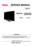
LED TV
Model No. LE19B3320
MSD3393
Chassis
WARNING
This service information is designed for experienced repair technicians only and is not designed for use by the general public.
It does not contain warnings or cautions to advise non-technical individuals of potential dangers in attempting to service a product.
Products powered by electricity should be serviced or repaired only by experienced professional technicians. Any attempt to
service or repair the product or products dealt with in this service information by anyone else could result in serious injury or death.
Service Manual
Model No.:
Chapter 1: General Information
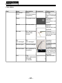
1-1. Table of Contents
1. General Information...........................................................................1
1-1. Table of Contents
1-2. General Guidelines
1-3. Important Notice
1-4. How to Read this Service Manual
1
3
3
6
6SHFL¿FDWLRQV.................................................................................... 6
3. Location of Controls and Components........................................... 8
3-1. Board Location
8
3-2. Main Board & AV Board
8
10
3-3. LCD Panel
4. Disassemble and Assemble.......................................................... 12
4-1 Remove the Pedestal
12
4-2 Remove the Back Cover
4-3 Remove the Adhesive Tape
4-4 Remove the Main Board
4-5 Remove the Speaker
4-6 Remove the Remote Control Board
12
12
13
13
14
5. Installation Instructions..…....………………...........…………......... 15
5-1 External Equipment Connections
15
5-2 HDMI Connections
19
6. Operation Instructions....…....………………...........…………......... 22
6-1 Front Panel Controls
22
6-2 Back Panel Controls
22
6-3 Universal Remote Control
23
7. Electrical Parts…....………………...........…………......................... 24
7-1. Block Diagram
7-2. Circuit Diagram
24
25
7-3. Wiring Connection Diagram
31
- 01 -
Service Manual
Model No.:
8. Measurements and Adjustments........…………............................ 32
8-1. How to enter into the factory model
35
8-2. How to update software
8-3. How to enter into the Hotel Model
36
37
9. Trouble-shooting………….............................................................. 38
9-1. Simple Check
38
9-2. Main Board Failure Check
39
9-3. Panel Failure
48
- 02 -
Service Manual
Model No.:
1-2. General Guidelines
When servicing, observe the original lead dress. If a short circuit is found, replace all parts
which have been overheated or damaged by the short circuit.
After servicing, see to it that all the protective devices such as insulation barriers, insulation
papers shields are properly installed.
After servicing, make the following leakage current checks to prevent the customer from
being exposed to shock hazards.
1) Leakage Current Cold Check
2) Leakage Current Hot Check
3) Prevention of Electro Static Discharge (ESD) to Electrostatically Sensitive
1-3. Important Notice
1-3-1. Follow the regulations and warnings
Most important thing is to list up the potential hazard or risk for the service personnel to
open the units and disassemble the units. For example, we need to describe properly
how to avoid the possibility to get electrical shock from the live power supply or charged
electrical parts (even the power is off).
This symbol indicates that high voltage is present inside.It is dangerous to
make any king of contact with any inside part of this product.
This symbol indicates that there are important operating and maintenance
instructions in the literture accompanying the appliance.
1-3-2. Be careful to the electrical shock
7RSUHYHQWGDPDJHZKLFKPLJKWUHVXOWLQHOHFWULFVKRFNRU¿UHGRQRWH[SRVHWKLV79VHW
to rain or excessive moisture. This TV must not be exposed to dripping or splashing water,
DQGREMHFWV¿OOHGZLWKOLTXLGVXFKDVYDVHVPXVWQRWEHSODFHGRQWRSRIRUDERYHWKH79
1-3-3. Electro static discharge (ESD)
Some semiconductor (solid state) devices can be damaged easily by static electricity. Such
components commonly are called Electrostatically Sensitive (ES) Devices. The following
techniques should be used to help reduce the incidence of component damage caused by
electros static discharge (ESD).
1-3-4. About lead free solder (PbF)
This product is manufactured using lead-free solder as a part of a movement within the
consumer products industry at large to be environmentally responsible. Lead-free solder
must be used in the servicing and repairing of this product.
8VHWKHJHQHZLQJSDUWVVSHFL¿HGSDUWV
Special parts which have purposes of fire retardant (resistors), high-quality sound
(capacitors), low noise (resistors), etc. are used.
When replacing any of components, be sure to use only manufacture's specified parts
shown in the parts list.
Safety Component
Ɣ&RPSRQHQWVLGHQWL¿HGE\PDUNKDYHVSHFLDOFKDUDFWHULVWLFVLPSRUWDQWIRUVDIHW\
- 03 -
Service Manual
Model No.:
1-3-6 Safety Check after Repairment
&RQ¿UPWKDWWKHVFUHZVSDUWVDQGZLULQJZKLFKZHUHUHPRYHGLQRUGHUWRVHUYLFHDUHSXW
in the original positions, or whether there are the positions which are deteriorated around
the serviced places serviced or not. Check the insulation between the antenna terminal or
external metal and the AC cord plug blades. And be sure the safety of that.
General Servicing Precautions
1. Always unplug the receiver AC power cord from the AC power source before;
a. Removing or reinstalling any component, circuit board module or any other receiver
assembly.
b. Disconnecting or reconnecting any receiver electrical plug or other electrical
connection.
c. Connecting a test substitute in parallel with an electrolytic capacitor in the receiver.
CAUTION: A wrong part substitution or incorrect polarity installation of electrolytic
capacitors may result in an explosion hazard.
2. Test high voltage only by measuring it with an appropriate high voltage meter or other
voltage measuring device (DVM, FETVOM, etc) equipped with a suitable high voltage
probe.
Do not test high voltage by "drawing an arc".
3. Do not spray chemicals on or near this receiver or any of its assemblies.
4. Unless specified otherwise in this service manual, clean electrical contacts only by
applying the following mixture to the contacts with a pipe cleaner, cotton-tipped stick or
comparable non-abrasive applicator; 10% (by volume) Acetone and 90% (by volume)
isopropyl alcohol (90%-99% strength).
CAUTION:7KLVLVDÀDPPDEOHPL[WXUH
8QOHVVVSHFL¿HGRWKHUZLVHLQWKLVVHUYLFHPDQXDOOXEULFDWLRQRIFRQWDFWVLVQRWUHTXLUHG
Capacitors may result in an explosion hazard.
5. Do not defeat any plug/socket B+ voltage interlocks with which receivers covered by this
service manual might be equipped.
6. Do not apply AC power to this instrument and/or any of its electrical assemblies unless
all solid-state device heat sinks are correctly installed.
7. Always connect the test receiver ground lead to the receiver chassis ground before
connecting the test receiver positive lead.
Always remove the test receiver ground lead last. Capacitors may result in an explosion
hazard.
8VHZLWKWKLVUHFHLYHURQO\WKHWHVW¿[WXUHVVSHFL¿HGLQWKLVVHUYLFHPDQXDO
CAUTION: 'RQRWFRQQHFWWKHWHVW¿[WXUHJURXQGVWUDSWRDQ\KHDWVLQNLQWKLVUHFeiver.
9. Remove the antenna terminal on TV and turn on the TV.
10. Insulation resistance between the cord plug terminals and the eternal exposure metal
should be more than Mohm by using the 500V insulation resistance meter.
11. If the insulation resistance is less than M ohm, the inspection repair should be required.
If you have not the 500V insulation resistance meter, use a Tester. External exposure
metal: Antenna terminal Headphone jack
- 04 -
Service Manual
Model No.:
Electrostatically Sensitive (ES) Devices
Some semiconductor (solid-state) devices can be damaged easily by static electricity.
Such components commonly are called Electrostatically Sensitive (ES) Devices.
Examples of typical ES devices are integrated circuits and some field-effect transistors
and semiconductor "chip" components. The following techniques should be used to help
reduce the ncidence of component damage caused by static by static electricity.
1. Immediately before handling any semiconductor component or semiconductorequipped assembly, drain off any electrostatic charge on your body by touching a known
earth ground. Alternatively, obtain and wear a commercially available discharging wrist
strap device, which should be removed to prevent potential shock reasons prior to applying
power to the unit under test.
2. After removing an electrical assembly equipped with ES devices, place the assembly
on a conductive surface such as aluminum foil, to prevent electrostatic charge buildup or
exposure of the assembly.
3. Use only a grounded-tip soldering iron to solder or unsolder ES devices.
4. Use only an anti-static type solder removal device. Some solder removal devices not
FODVVL¿HGDVDQWLVWDWLFFDQJHQHUDWHHOHFWULFDOFKDUJHVVXI¿FLHQWWRGDPDJH(6GHYLFHV
'RQRWXVHIUHRQSURSHOOHGFKHPLFDOV7KHVHFDQJHQHUDWHHOHFWULFDOFKDUJHVVXI¿FLHQW
to damage ES devices.
6. Do not remove a replacement ES device from its protective package until immediately
before you are ready to install it.
(Most replacement ES devices are packaged with leads electrically shorted together by
conductive foam, aluminum foil or comparable conductive material).
7. Immediately before removing the protective material from the leads of a replacement
ES device, touch the protective material to the chassis or circuit assembly into which the
device will be installed.
CAUTION: Be sure no power is applied to the chassis or circuit, and observe all other
safety precautions.
8. Minimize bodily motions when handling unpackaged replacement ES devices.
(Otherwise harmless motion such as the brushing together of your clothes fabric or the
OLIWLQJRI\RXUIRRWIURPDFDUSHWHGÀRRUFDQJHQHUDWHVWDWLFHOHFWULFLW\VXI¿FLHQWWRGDPDJH
an ES device.)
1-3-7. Ordering Spare Parts
Please include the following informations when you order parts. (Particularly the Version
letter)
1. Model number, Serial number and Software Version
The model number and Serial number can be found on the back of each product and the
Software Version can be found at the Spare Parts List.
2. Spare Part No. and Description
<RXFDQ¿QGWKHPLQWKH6SDUH3DUWV/LVW
- 05 -
Service Manual
Model No.:
1-3-8. Photo used in this manual
The illustration and photos used in this Manual may not base on the final design of
products, which may differ from your products in some way.
1-4. How to Read this Service Manual
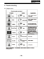
Using Icons:
,FRQVDUHXVHGWRDWWUDFWWKHDWWHQWLRQRIWKHUHDGHUWRVSHFL¿FLQIRUPDWLRQ7KHPHDQLQJRI
each icon is described in the table below:
Note:
A “note” provides information that is not indispensable, but may nevertheless be valuable
to the reader, such as tips and tricks.
Caution:
A “caution” is used when there is danger that the reader, through incorrect manipulation,
may damage equipment, loose data, get an unexpected result or has to restart(part of) a
procedure.
Warning:
A “warning” is used when there is danger of personal injury.
Reference:
A “reference” guides the reader to other places in this binder or in this manual, where he/
VKHZLOO¿QGDGGLWLRQDOLQIRUPDWLRQRQDVSHFL¿FWRSLF
- 06 -
Service Manual
Model No.:
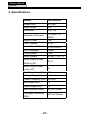
6SHFL¿FDWLRQV
Model
LE19B3320
Screen Size
18.5 inch
Aspect Ratio
16:9
Resolution
1366*768
Response Time (ms)
5.0 (GRAY TO
GRAY)
Angel of View
176o
Color Display
16.7M
No. of Preset Channels
Cable :1-135/
Air: 2-69 (ATV&DTV)
OSD Language
English
Color System
NTSC
Audio System
DK, BG, I, M, L, L'
Audio Output Power
(Built-in) (W)
3W×2
Audio Output Power
(outer) (W)
No
Total Power Input (W)
30W
Voltage Range (V)
AC 100-240V
Power Frequency (Hz) 50~60Hz
Net Weight (KG)
2.8
Gross Weight (KG)
3.9
Net Dimension (MM)
465*38*316mm
Packaged Dimension
(MM)
465*165*349mm
- 07 -
Service Manual
Model No.:
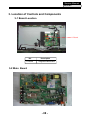
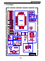
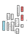
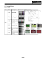
3. Location of Controls and Components
3-1 Board Location
A Board
No.
A Board
Description
Integration Mainboard
3-2 Main Board
- 08 -
Service Manual
Model No.:
3-2-1 Function Description:
Main Board
Process signal which incept from exterior equipment then translate into signal that panel
can display.
&RQQHFWRUGH¿QLWLRQ
Main board connector
Keypad andremote connector (J2)
Pin number
1
2
3
4
5
6
Signal name
LED_R
LED_G
Description
LAMP RED
LAMP GREEN
STANDBY
IR
GND
5V
7
8
9
10
REMOTE CONTROL
GND
POWER FOR REMOTE
NC
KEY0
KEY1
GND
Speaker connector (J17)
Pin number
1
2
3
4
Signal name
RSPK+
RSPKLSPKLSPK+
Description
RSPK+
RSPKLSPKLSPK+
- 09 -
Service Manual
Model No.:
3-3. LED Panel
MTC185LED-D01H(PANDA:LC185TT2A)
- 10 -
Service Manual
Model No.:
3-4-1.Connector de finition
Pin No.
Symbol
Function
Remark
1
RxOIN0-
Negative LVDS DATA input(ODD)
LVDS
2
RxOIN0+
Positive LVDS DATA input(ODD)
LVDS
3
RxOIN1-
Negative LVDS DATA input(ODD)
LVDS
4
RxOIN1+
Positive LVDS DATA input(ODD)
LVDS
5
RxOIN2-
Negative LVDS DATA input(ODD)
LVDS
6
RxOIN2+
Positive LVDS DATA input(ODD)
LVDS
7
GND
Ground
8
RxOCLK-
Negative LVDS Clock input(ODD)
LVDS
9
RxOCLK+
Positive LVDS Clock input(ODD)
LVDS
10
RxOIN3-
Negative LVDS DATA input(ODD)
LVDS
11
RxOIN3+
Positive LVDS DATA input(ODD)
LVDS
12
RxEIN0-
Negative LVDS DATA input(EVEN)
LVDS
13
RxEIN0+
Positive LVDS DATA input(EVEN)
LVDS
14
GND
Ground
15
RxEIN1-
Negative LVDS DATA input(EVEN)
LVDS
16
RxEIN1+
Positive LVDS DATA input(EVEN)
LVDS
17
GND
Ground
18
RxEIN2-
Negative LVDS DATA input(EVEN)
LVDS
19
RxEIN2+
Positive LVDS DATA input(EVEN)
LVDS
20
RxCLK-
Negative LVDS Clock input(EVEN)
LVDS
21
RxCLK+
Positive LVDS Clock input(EVEN)
LVDS
22
RxEIN3-
Negative LVDS DATA input(EVEN)
LVDS
23
RxEIN3+
Positive LVDS DATA input(EVEN)
LVDS
24
GND
Ground
25
NC
No connection(Do not connect)
26
NC
No connection(Do not connect)
27
NC
No connection, This pin should be open
28
VDD
POWER +5V
29
VDD
POWER +5V
30
VDD
POWER +5V
[Note 1]
[Note 1] Built-in Self Test (BIST)
*1) PIN27=NC: Disable BIST function.
Available LVDS Signal input: Display LVDS input Pattern.
*2)
1) Keep the NC Pin and don’t connect it to GND or other signals.
2) GND Pin must connect to the ground, don’t let it be a vacant pin.
Available LVDS Signal input: Display LVDS input Pattern.
No LVDS Signal or unavailable LVDS Signal input: Display BIST Pattern
- 11 -
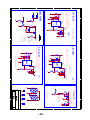
Service Manual
Model No.:
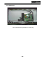
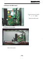
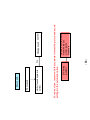
4. Disassemble and assemble
4-1 Remove the Pedestal
/D\GRZQWKHXQLWVRWKDWUHDUFRYHU
faces upward
5HPRYH WKH WKUHH VFUHZ IURP WKH
UHDUFRYHULQGLFDWHGZLWKż
7KHQUHPRYHWKHSHGHVWDO
4-2Remove the Back Cover
5HPRYHWKHWKHVHVFUHZLQGLFDWHGRQ
¿JXUHDERYHE\ż
7KHQUHPRYHWKHEDFNFRYHUIURPWKH
unit.
4-3. Remove the adhesive tape
Remove the adhesive tape indicated on the
¿JXUHDERYH
- 12 -
Service Manual
Model No.:
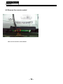
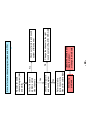
4-4 Remove the Main board
'LVFRQQHFWHG WKH FRXSOHU
J2
J1 J17 CN800
5HPRYHWKH0DLQERDUG
4-5 Remove the speaker
Take out the speaker
- 13 -
Service Manual
Model No.:
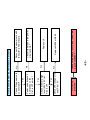
4-6 Remove the remote control
take out the remote control board
- 14 -
Service Manual
Model No.:
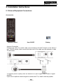
5. Installation Instructions
5-1 External Equipment Connections
Accessories
Remote Control
User GUIDE
Battery
Antenna Connection
Connect one end of a coaxial cable (not included) to the ANT IN jack on the back of
your TV/DVD combo, then connect the other end of the cable into the antenna or cable
TV wall outlet.
To improve picture quality from an antenna in a poor signal area, install a signal
DPSOL¿HU
If you need to split the antenna signal to connect two TVs, install a two-way splitter.
- 15 -
- 16 -
- 17 -
- 18 -
Service Manual
Model No.:
5-2 HDMI Connections
When the source device(DVD player or Set Top Box) supports HDM
How To Connect
1. Connect the source device to HDMI port of this TV with an HDMI cable(not supplied
with this product).
2. No separated audio connection is necessary.
How To Use
If the source device supports Auto HDMI function, the output resolution of the source
device will be automatically
set to 1280x720p.
If the source device does not support Auto HDMI, you need to set the output resolution
appropriately.
To get the best picture quality, adjust the output resolution of the source device to
1280x720p.
Select HDMI input source in input source option of Select Main source menu.
When the source device(DVD player or Set Top Box) supports DVI
How To Connect
1. Connect the source device to HDMI port of this TV with a HDMI-to-DVI cable(not
supplied with this product).
2. A separated audio connection is necessary.
3. If the source device has an analog audio output connector, connect the source device
audio output to DVI Audio In port located on the PC port.
How To Use
If the source device supports Auto DVI function, the output resolution of the source device
will be automatically
set to 1280x720p.
If the source device does not support Auto DVI, you need to set the output resolution
appropriately.
To get the best picture quality, adjust the output resolution of the source device to
1280x720p.
Press the INPUT button to select HDMI input source in input source option of Select Main
source menu.
Installation
- 19 -
Service Manual
Model No.:
Cable sample
HDMI Cable
(not supplied with the product)
HDMI to DVI Cable
( not supplied with the product)
Analog Audio Cable
(Stereo to RCA type)
(not supplied with the product)
-20 -
Service Manual
Model No.:
Power source
TO USE AC POWER SOURCE
Use the AC polarized line cord provided for operation on AC.
Insert the AC cord plug into a standard polarized AC outlet.
NOTES:
Ŷ1HYHUFRQQHFWWKH$&OLQHFRUGSOXJWRRWKHUWKDQWKHVSHFL¿HGYROWDJH
Use the attached power cord only.
Ŷ,IWKHSRODUL]HG$&FRUGGRHVQRW¿WLQWRDQRQSRODUL]HG$&RXWOHW
GRQRWDWWHPSWWR¿OHRUFXWWKHEODGH,WLVWKHXVHUCVUHVSRQVLELOLW\WRKDYHDQ
electrician replace the obsolete outlet.
Ŷ,I\RXFDXVHDVWDWLFGLVFKDUJHZKHQWRXFKLQJWKHXQLWDQGWKHXQLWIDLOVWRIXQFWLRQ
simply unplug the unit from the AC outlet and plug it back in. The unit should return to
normal operation.
- 21 -
Service Manual
Model No.:
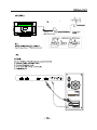
6. Operation Instructions
Basal information
- 22 -
Service Manual
Model No.:
6-3 Setting Up Your Remote Control
- 23 -
Model No.:
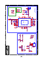
7. Electrical parts
4
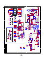
7-1. Block Diagram
/0!
1!
5
AC100V-240V
PWM IC
Q807
(0B2273)
TRANSFORMER
T102
DC/DC
U2
RT8296A
5VSTB
RF IN
Q809
4
3.3VA
PWR-ON/OFF
QM3014D 5VA
12VA
AUDIO AMP.
EUA2113 UD3
YD1517 UD10
ATSC TUNER
TDA18273 (ONBOARD)
UD12
OR
601
UD7
SY8008B
DC/DC
UD9
3
IF
3.3V_TUNER
3.3VA
+3.3Vstb
1.15V
1.8VA
AL0O/AR0O
UD13
SY8008B
DC/DC
UD8
DC/DC
SY8008B
3.3V_TUNER
PANEL_POWER
J18
JACK
HeadPhone
PANEL_ON/OFF
L/R
2
DVD_CVBS
CN402
Title
Custom
Size
Date:
CVBS1
LINEIN_L1/R1
YPbPr0
BLOCK DIAGRAM
Monday, January 07, 2013
MSAV3216-K6
Document Number
Sheet
1
1
FRONT
PANEL
AV
PH1~3
VGA
AUDIO
J8
VGA
PH1~3
HDMI*3
PH1~3
YPbPr
2
of
12
31-32F XINGHESHIJI BLDG. 3069 CAITIAN ROAD FUTIAN DISTRICT SHENZHEN
ShenZhen MTC Co., Ltd.
L/R (AIN0)
RGB
IR,KEY0,KEY1
BLOCK DIAGRAM
DSP
32Mbit
SPI FLASH
J3
SPIDF
OUTPUT
COAXIAL
U1
MSD3393-128PIN
USB PORT
J13
2
Rev
A
D
C
B
A
- 24 -
EFD25
+12V
Q806
QM3005D
J17
TO SPK
5VA
CVBS0
D
C
B
A
3
LINEIN_L0/R0
Model No.:
7-2. Circuit Diagtam
5
4
3
2
HDMI Interface
HDMI2-RX0P
HDMI2-RX0N
HDMI2-RX1P
HDMI2-RX1N
HDMI2-RX2P
HDMI2-RX2N
HDMI2-CLKN
HDMI2-CLKP
HDMI2-SCL
HDMI2-SDA
HDMI2-HPDIN
MHL_CABLE-DET
HDMI2-RX0P
HDMI2-RX0N
HDMI2-RX1P
HDMI2-RX1N
HDMI2-RX2P
HDMI2-RX2N
HDMI2-CLKN
HDMI2-CLKP
HDMI2-SCL
HDMI2-SDA
HDMI2-HPDIN
MHL_CABLE-DET
+3.3V_Normal
HDMI1-CLKN
HDMI1-CLKP
HDMI1-RX0N
HDMI1-RX0P
HDMI1-RX1N
HDMI1-RX1P
HDMI1-RX2N
HDMI1-RX2P
VGA_HSYNC
RGB0_B+
RGB0_G+
RGB0_GRGB0_R+
VGA_VSYNC
HDMI-ARC
HDMI-CEC
HDMI-ARC
HDMI-CEC
PC & YPBPR Interface
VGA-Rin
VGA-Gin
VGA-Bin
R102
R103
R134
R135
33R C100 47nF RGB0_R+
68R C104 47nF RGB0_G33R C103 47nF RGB0_G+
33R C170 47nF RGB0_B+
R123
R129
R130
R131
R111
33R C105
68R C106
33R C108
33R C164
0R C162
+3.3V_Normal
RGB1_B+
RGB1_SOG
RGB1_G+
RGB1_GRGB1_R+
VGA_HSYNC
VGA_VSYNC
VGA_HSYNC
VGA_VSYNC
YPbPr_PR
YPbPr_Y
YPbPr_PB
CVBS1+
CVBS0+
CVBS_VCOM
47nF RGB1_R+
47nF RGB1_G47nF RGB1_G+
47nF RGB1_B+
1nF RGB1_SOG
VDDC
+3.3V_AU
LINEIN_R0
LINEIN_L0
LINEIN_R1
LINEIN_L1
AU_VAG
AU_VRM
CVBS IN & OUT
R138
SIDE_AV
DVD_AV
C
33R C174 47nF CVBS1+
R115
33R C110 47nF
R117
CVBS_VCOM
68R C111 47nF
1
2
3
4
5
6
7
8
9
10
11
12
13
14
15
16
17
18
19
20
21
22
23
24
25
26
27
28
29
30
31
32
33
34
35
36
37
38
VDDC
C135
0.1uF
C141
0.1uF
C136
0.1uF
C156
0.1uF
D
DDR2 1.8V
E-PAD
Test
MARK
MARK
RX0P_B
RX0N_B
RXCP_B
RXCN_B
RX2P_D
RX2N_D
RX1P_D
RX1N_D
RX0P_D
RX0N_D
RXCP_D
RXCN_D
VDDC/AVDDL_DVI
GND_EFUSE
AVDD_5V
HOTPLUG_B
DDCDB_CL
DDCDB_DA
MHL_DET
DDCDA_DA
DDCDA_CL
DDCDC_DA
DDCDC_CL
VDDIO_DATA
VDDC/DVDD_DDR_DATA
SAR2
U1
HDMI2-RX1N
HDMI2-RX1P
HDMI2-RX2N
HDMI2-RX2P
C129
2.2uF
CC0603
132
131
130
129
128
127
126
125
124
123
122
121
120
119
118
117
116
115
114
113
112
111
110
109
108
107
106
105
104
103
HDMI1-RX0P
HDMI1-RX0N
HDMI1-RX1P
HDMI1-RX1N
HDMI1-RX2P
HDMI1-RX2N
HDMI1-CLKN
HDMI1-CLKP
HDMI1-SCL
HDMI1-SDA
HDMI1-HPDIN
HDMI1-RX0P
HDMI1-RX0N
HDMI1-RX1P
HDMI1-RX1N
HDMI1-RX2P
HDMI1-RX2N
HDMI1-CLKN
HDMI1-CLKP
HDMI1-SCL
HDMI1-SDA
HDMI1-HPDIN
AVDD5V_MHL
HDMI2-HPDIN
HDMI2-SCL
HDMI2-SDA
MHL_CABLE-DET
HDMI1-SDA
HDMI1-SCL
HDMI0-SDA
HDMI0-SCL
+1.8V_DDR2
VDDC
AMP-MUTE
HDMI2-RX0P
HDMI2-RX0N
HDMI2-CLKP
HDMI2-CLKN
HDMI0-RX2P
HDMI0-RX2N
HDMI0-RX1P
HDMI0-RX1N
HDMI0-RX0P
HDMI0-RX0N
HDMI0-CLKP
HDMI0-CLKN
VDDC
RX1N_B
RX1P_B
RX2N_B
RX2P_B
AVDD_MOD
RXCN_A
RXCP_A
RX0N_A
RX0P_A
RX1N_A
RX1P_A
RX2N_A
RX2P_A
HSYNC0
BIN0P
GIN0P
GIN0M
RIN0P
VSYNC0
AVDD3P3_ADC
BIN1P
SOGIN1
GIN1P
GIN1M
RIN1P
VSYNC1
CVBS1
CVBS0
VCOM
CVBS_OUT1
VDDC
AVDD_AU33
AUR0
AUL0
AUR1
AUL1
VAG
VRM
MSD3393LU
CVBS0+
3.3V audio
+1.8V_DDR2
+3.3V_Normal
L105
KEY1
KEY0
102
101
100
99
98
97
96
95
94
93
92
91
90
89
88
87
86
85
84
83
82
81
80
79
78
77
76
75
74
73
72
71
70
69
68
67
66
65
SAR1
SAR0
AVDD_MOD
DP_P1
DM_P1
DP_P0
DM_P0
RESET
INT/GPIO64
IRIN
CEC
TEST
DDCA_CK
DDCA_DA
ARC
SPI_CK
SPI_CZ
SPI_DI
SPI_DO
PWM0
PWM1
HOTPLUG_A
HOTPLUG_C/D
LDE/LVB0M
LCK/LVB0P
LVB1M
LVB1P
LVB2M
LVB2P
AVDD_MOD
LVB3M
LVB3P
LVA0M
LVA0P
LVA1M
LVA1P
LVA2M
LVA2P
AUL4
AUR4
AUOUTL3
AUOUTR3
AUOUTL0
AUOUTR0
IFAGC
VIFP
VIFM
AVDD3P3_DADC
AVDD3P3_DMPLL
XIN
Xout
AVDD_MOD
VDDIO_CMD
VDDC/DVDD_DDR_CMD
GPIO0/GPIO44
GPIO1/GPIO45
GPIO2/GPIO46
GPIO3/GPIO47
GPIO4/GPIO48
GPIO5/GPIO49
LVA3P
LVA3M
LVACKP
LVACKM
D
VDDC 1.2V
HDMI0-RX0P
HDMI0-RX0N
HDMI0-RX1P
HDMI0-RX1N
HDMI0-RX2P
HDMI0-RX2N
HDMI0-CLKN
HDMI0-CLKP
HDMI0-SCL
HDMI0-SDA
HDMI0-HPDIN
HDMI0-RX0P
HDMI0-RX0N
HDMI0-RX1P
HDMI0-RX1N
HDMI0-RX2P
HDMI0-RX2N
HDMI0-CLKN
HDMI0-CLKP
HDMI0-SCL
HDMI0-SDA
HDMI0-HPDIN
1
C120
2.2uF
+3.3V_Normal
USB1_D+
USB1_DUSB2_D+
USB2_DSystem-RST
VBL_CTRL
IR-in
HDMI-CEC
C121
0.1uF
3.3V MPLL
+3.3V_Normal
+3.3V_AU
FB
C122
0.1uF
L106
+3.3V_PLL
FB
C155
0.1uF
C151
0.1uF
3.3V
UART-RX
UART-TX
HDMI-ARC
SPI_Flash-SCK
SPI_Flash-CSN
SPI_Flash-SDI
SPI_Flash-SDO
PWM0
PWM1
HDMI1-HPDIN
HDMI0-HPDIN
R7_RXO0R6_RXO0+
R5_RXO1R4_RXO1+
R3_RXO2R2_RXO2+
+3.3V_ADC
+3.3V_Normal
FB
L104
C153
2.2uF
CC0603
C161
0.1uF
C154
0.1uF
C146
0.1uF
C152
0.1uF
C159
2.2uF C142
CC0603 0.1uF
C147
0.1uF
Audio Line Out
+3.3V_Normal
G7_RXO3G6_RXO3+
G3_RXE0G2_RXE0+
G1_RXE1G0_RXE1+
B7_RXE2B6_RXE2+
C
39
40
41
42
43
44
45
46
47
48
49
50
51
52
53
54
55
56
57
58
59
60
61
62
63
64
MSD3393LU
AUDIO IN
C127 2.2uF LINEIN_L4
C128 2.2uF LINEIN_R4
TUNER_SDA
TUNER_SCL
DVD_ON/OFF
ARC_DET
PWR-ON/OFF
SPDIF_OUT
B2_RXE3+
B3_RXE3B4_RXEC+
B5_RXEC-
VGA-Lin_AU
VGA-Rin_AU
VGA-Lin_AU
VGA-Rin_AU
XTALI
XTALO
C124 2.2uF LINEIN_L1
C123 2.2uF LINEIN_R1
IFAGC
VIFP
VIFM
C176 2.2uF LINEIN_L0
C175 2.2uF LINEIN_R0
VDDC
+1.8V_DDR2
+3.3V_Normal
DVD_IN_L
+3.3V_PLL
+3.3V_ADC
DVD_IN_R
SIDE_AV_L
SIDE_AV_R
DVD_IN_L
DVD_IN_R
SIDE_AV_L
SIDE_AV_R
LINEIN_L4
LINEIN_R4
LINE3OUT_L
LINE3OUT_R
LINE3OUT_L
LINEOUT_APML
C172
1nF
R155
220K
C178
1nF
R153
220K
LINE3OUT_R
LINEOUT_APMR
DIF IN
DIF_P
C165 VIFP
DIF_N
C166 VIFM
Close to Mstar IC
DPin57J"# MHL_VBUS-EN EKDVD_ON/OFF
0.1uF
LVDS CONNECTOR
0.1uF
USB & SPDIF_OUT
AU_VRM
AU_VAG
USB2_DUSB2_D+
USB2_DUSB2_D+
C167 C169 C168
USB1_DUSB1_D+
USB1_DUSB1_D+
2.2uF 2.2uF 0.1uF
SPDIF_OUT
R128
10K
L100
FB
SPDIF_OUT
Close to Mstar IC
RESET
IFAGC
R133
IFAGC-T
ARC_DET? AMP-MUTE @ A / 0 B C D AMP-MUTE/ 0 E F G PMH I / 0 C163
5Vstb
2
4
6
8
10
12
14
16
G2_RXE0+
18
G0_RXE1+
20
B6_RXE2+
22
B4_RXEC+
24
B2_RXE3+
26
28
30
32
VCC-Panel
34
36
38
PANEL_ON/OFF 40
3
22nF
2
R230
10K 1
XTAL
C275
2.2uF
C1=C2=2*CL-5
C276
2.2uF
&'()*+
$*,-.
R232
100K
C126
15pF
R132
1M
R231
System-RST
1K
CHIP_CONFIG
{IPAD_PWM1, PAD_PWM0}
B51_NO_EJ
4'h00
C1
XTALO R127 0R
Q201
3906
3
B
2
D201
BAV99
1
R227
1M
C2
PWM1
R165
4.7K
PWM0
R166
4.7K
NC/4.7KDVD_ON/OFF
R280
4.7K
AMP-MUTE
+3.3V_Normal
RD41
1K
LCD_OP#
VCC-Panel
RD46
OVERDRIVER
NC/0R
B
R281
+3.3V_Normal
R282 R283
4
3
2
1
15pF
4.7K 4.7K
TUNER_SCL
TUNER_SDA
4p,GND
LED
DEBUG
G3_RXE0G1_RXE1B7_RXE2B5_RXECB3_RXE3-
H1
C125
XTALI
NOTE:30PPM
R279
R7_RXO0R5_RXO1R3_RXO2B5_RXECG7_RXO3-
10K
Y1
24.000MHz
C277
1nF
+3.3V_Normal
1
3
5
7
9
11
13
15
17
19
21
23
25
27
29
31
33
35
37
39
GND GND
RO0+RO0RO1+RO1RO2+RO2ROC+ROCRO3+RO3RO4+RO4GND GND
RE0+ RE0RE1+ RE1RE2+ RE2REC+RECRE3+ RE3RE4+ RE4GND GND
GND
LCDOP
VCC VCC
VCC VCC
VCC VCC
OP2 OP1
R6_RXO0+
R4_RXO1+
R2_RXO2+
B4_RXEC+
G6_RXO3+
AMP-MUTE
TUNER_SCL
TUNER_SDA
AMP-MUTE
TUNER_SCL
TUNER_SDA
0R
J1
2*20Pin-2.0mm
PWR-ON/OFF
PWM0
PWM1
VBL_CTRL
DVD_ON/OFF
ARC_DET
PWR-ON/OFF
BRI_ADJ
ON_PANEL
VBL_CTRL
DVD_ON/OFF
ARC_DET
3.3V-TUNER
RD50
NC/4.7K
RD54 NC/33R
RD55 NC/33R
RD57
NC/0R
5Vstb
RD51
NC/4.7K
PANEL_ON/OFF
OVERDRIVER
RD58
NC/0R
5Vstb
MUST pull high to 5VSTB
R278
LED
PWR-ON/OFF
1K 1
Q202
3904
KEY&IR BOARD
+3.3Vstb
Q203
3904
5Vstb
KEY PAD
2
C278
100pF
1
RD42
RD43
UART_TX
UART_RX
LED_G
R248 4.7K
10K
10K
100R
100R
R242
100R
LED
PWR-ON/OFF LED_R
LED_G
IR-in
FOR TEST
RP11
KEY0
KEY1
CD49
1KKEY0-in
1KKEY1-in
1nF
CD48
RD52
RD53
CD50
CD51
SPI_Flash-SCK
SPI_Flash-CSN
SPI_Flash-SDI
SPI_Flash-SDO
33pF
SPI_SCK
SPI_CSN
SPI_SDI
SPI_SDO
CD47
RP33X4
SPI_SDI
SPI_SCK
VCC-FLASH
+3.3Vstb
1 3 5 7
5
6
7
8
2 4 6 8
4
TF4 TF1 TF5
FLASH_WP0N
3
TF6
SPI_SDO 2 TF3
SPI_CSN 1 TF2NC/TPTF7
TF1
TF8
IR
10
9
8
7
6
5
4
3
2
1
RD47
RD48 10R
10R
RD49
1KIRDAT
10
9
8
7
6
5
4
3
2
1
J2
100pF
100pF
FLASH
1nF
UART-TXR136
UART-RXR137
NC/4.7K
4.7K
4.7K
LED_R
3
4.7K
R240
R236
4.7K
R239
RD44
RD45
ON
OFF
4.7K
10R
R202
3
R201
2
ISP AND VGA EDID
+3.3Vstb
5Vstb
A
A
+3.3Vstb
R157
R152
59:;<=>
U18
C41
10uF
IRIN
IRDAT
4.7K
10K
SPI_CSN
1
SPI_SDO
2
FLASH_WP0N
3
4
CE#
VDD
SO HOLD#
WP#
SCK
VSS
SI
R146
8
7
VCC-FLASH
6
SPI_SCK
5
SPI_SDI
27R
C158
0.1uF
EN25F32
FLASH_WP
Title
!"#$%
MSD3393
Size
Custom
Date:
Document Number
Rev
1.0
MAIN CHIP
Friday, January 04, 2013
Sheet
2
of
9
1
- 25 -
D
5
1.15V DC-DC
4
VIN
UD9
SY8008D
SY8008D
OUT/FB
LX
5
3
10uF
CD95
0.1uF
+
EC113
4
220uF/16V
RD61
2.2K
Vpp=100mV
56231
+12V1251.3mA
+5V1583mA
VCC-Panel
Vout=0.6X(1+R up/R down)
LD23
4.7uH_2A
RD143
47K
100K
RD146
QD6 AO3407
47K 10uF
RD137 CD89 CD94
526MA
1.12V~1.18V -./011.158V
-.231Irms=464.3mAImax=575mA
1.15V
1.164VVDDC
5Vstb
LD24 600Ω-1.5A-0805
1
CD99 CD100 RD142
100K
CD98 10uF 10uF
0.1uF
EN
VCCLCDFN
RD62 270K
CD53 0.1uF
RD60
10K
3904
1.8V DC-DC
3
VIN
UD7
SY8008D
SY8008D
LX
OUT/FB
5
3
VIN
EN
UD8
SY8008D
SY8008D
LX
OUT/FB
3
5
4.7uH_2A
RD145
RD141
330K
1.8VA
2
139MA
+1.8V_DDR2
+3.3V_Normal
150MA
RD135 CD96 CD85 CD86
120K
10uF
0.1uF
RD139
82K
RD136 CD97 CD87 CD88
120K 10uF
10uF 0.1uF
10uF
4.7uH_2A
1.812V
LD21
1.7V~1.9V -./011.834V
1
RD138
100K
4
-.231Irms=167.3mAImax=206mA
5VA
CD101 CD91
LD25 600Ω-1.5A-0805
CD90
10uF
EN
RD144
100K
<1A 5V Input--->Output 1.8V
100pF
CD103
10uF
0.1uF
3.3V DC-DC
4
3.14V~3.46V -./013.33V
&'(4-.231Irms=123.1mAImax=288mA
LD22
+3.3Vstb
5Vstb
LD26 600Ω-1.5A-0805
1
CD102 CD93 RD140
100K
CD104
CD92 10uF 10uF
0.1uF
+3.3V_Normal
R224
4.7K
R30 10K
6
7
8
9
AO3407
1uF
C139
1
of
9
0.1uF
C130
3.3V_TUNER
silicon tuner FB2
1
H7
NC
10uF
C2
600Ω-1.5A-0805
78231 3.3V-TUNER
218mA
Q2
0.1uF
R215
9
8
7
6
Sheet
MSD3393
H6
NC
100K 2012.11.29
!"#3.3V-TUNER
$%&'(AGC)*+,
Q4
3904
H5
NC
NC
2
3
4
5
H3
1
C46
TUNER4-.231Irms=186.5mAImax=200mA
332mA MAX:360MA
2 PWR-ON/OFF
H:ON
L:OFF
H2
5
4
3
2
NC
H4
NC
Document Number
DC-DC
1
1
3
2
Tuesday, January 15, 2013
Rev
1.0
D
C
B
A
- 26 -
CD105
QD7
100K
Title
Size
Custom
Date:
1
100pF
0R
VCCLCDFN
1
100pF
2
1
GND
2
<1A 5V Input--->Output 3.3V
3
1
<1A 5V Input--->Output 1.15V
RD56
NC/0R
CD52
10uF
RD63
4.7K
78231
+12V12.06A
+5V11.41A
4
1
1
PANEL POWER
12VA
RD59
ON_PANEL
5VA
2
RD64
4.7K
3
2
C
B
A
5
GND
2
GND
2
1
2
3
1
2
3
4
5
6
1
2
3
4
5
6
5
SIDE-AU-R
SIDE-AU-L
YIN
PBIN
PRIN
1nF
CD64
1nF
CD65
10pF
RD100
RD107
FB_11_OHM_500MA
FB_11_OHM_500MA
FB_11_OHM_500MA
R713
10K
R702
10K
10K
10K
AV
10K
RD108
RD103
10K
RD109
75R
75R 75R
EC74
U702
PT2308P
N54562955
R743
15K
USB1_D2
2
5VA
1.5A_FUSH
DD4
LD14
NC/1.5A_FUSH
SIDE_CVBS
SIDE-AU-L
PH_L
PH_R
5VA
SIDE-AU-R
YIN
PBIN
PRIN
1K
CD66
10uF
CD67
5VUSB2
NC/10uF
5VUSB1
EC702
100uF/10V
10R
R706
1K
RD128
RD127
RCA
S
S
G
J3
2
2
2
SIDE_AV
2
2
3
2
1
2
SIDE_AV_L
SIDE_AV_R
YPbPr_Y
YPbPr_PB
22R
YPbPr_PR
R140
22R
+
AMP_RIN
0.1uF
C737
R141
5V_EAR
AMP_LIN
220uF/16V
EC75
220uF/16V
R744
15K
AMP_RIN
AMP_LIN
CD54
33pF
FB_11_OHM_500MA
75R
LD16
LD12
LD17
LD15
CD63
LD13
FB_11_OHM_500MA
SIDE_CVBS
AV INPUT
SIDE_CVBS
SIDE-AU-L
SIDE-AU-R
YIN
YPbPr INPUT
PBIN
PRIN
RD69
10uF
R707
10K
R708
10K
10uF
5V_EAR
USB1_D+
2
2
120R
RD70
75R
PH_DET
C745
10uF
C709
C710
Near MST.IC
USB2_D-
Ground in the middle of the L/R
USB2_D+
1
2
3
4
5
6
1
2
3
4
5
6
1
2
3
4
5
J19
J20
NC/AV-JACK-3/AV
6
5
4
3
2
1
NC/AV-JACK-3/AV
6
7
SIDE AV
J6
4
5
6
1
2
3
4
5
6
YPbPr
SPDIF_OUT
RD124
OTG_DM1
100R
OTG_DP1
4
J8
J5
CN402
15
5
10
14
4
9
13
3
8
12
2
7
11
1
6
1
4
5
2
3
6
DVD INPUT
1
2
3
4
5
6
7
7pin 2.0mm
VGA INPUT
2
2
2
VGA-Rin_AU
2
DVD_IN_R
DVD_IN_L
CN403
DVD_IN_R
DVD_IN_L
VGA-Lin_AU
100R UART_RX
R430
4pin 2.0mm
QD3
3906
DVD POWER
4.7K
VCC_AMP
JD2
1
2
NC/FOR 1517
RD148
FOR 2X3W
1
2
1RD7
RD147
12K
UART_TX
3
VSYNC
HSYNC
C29
220R
10uF 10uF
C28
RD13
ROUT+
ROUTLOUTLOUT+
IN4148
VGAB
100R
100R
GSCL
VGA_ARI
RD99
10K
12K
2 R429
UART_RX
RD71
RD72
IVS
VGA_ALI
UART_TX
100R
10K
100R
RD74
10K
RD95
RD96
RD98
10K
DVD_AV
LOUT+
2
QD1
3904
2
MUTE
IRIN
DVD_ON/OFF
4.7K
0R
HP_DET
Head Phone-MUTE
R906
MUTE
RD5
DVD-Rin
DVD-Lin
RD97
GSCL
IHS
GBLU
R433
100R
R435
1K
CD7
+
NC/220uF/16V
Q853
3904
R905
0R
ROUT+
AL+
NC/470uF/10V
2
AR+
NC/470uF/10V
2
NC/100uF/16V
CD107 NC/2.2uF
CD108
CD1091
CD1101
CD111 NC/2.2uF
NC/0R
5VA
VGAG
2
2
100R
4
3
2
1
RD77
100pF
100R
100R
RD4
10K
VCC_AMP
QD2
3904
RD12
0R
SVR
1uF
CD106
VCC_AMP
MUTE
NC/0R
RD11
10K
DD1
GSDA
GGRN
75R R D 8 3
VGAR
RD94
75R R D 82
100R
GSDA
10K R D 8 0
RD78
CD60
10K R D 79
GRED
CD62
R425
R426
100pF
DVD_AR
DVD_AL
1
10K
R428
75R
0R
RD9
1
2
3
4
5
6
7
8
9
10
47K
R427
NC/TPA1517
GND/HS
IN1
GND/HS
SGND
GND/HS
SVRR
GND/HS
OUT 1
GND/HS
PGND
GND/HS
OUT 2
GND/HS
VCC
GND/HS
M/SB
GND/HS
IN2
GND/HS GND/HS
UD10
MUTE Control
OFF
2 AMP-MUTE
ON
1517
20
19
18
17
16
15
14
13
12
11
RD1
DVD_CVBS
VGA Audio IN
PC_DB15HD_MIDDLE
16
17
7
YPbPr
SPDIF_OUT
Closed to IC
J18
OTG_DP
OTG_DM
5
8
8
8
8
8
RD114
7
7
7
AV-JACK-3/WO/-./
J7
2
SPDIF Output
C558
NC/33pF
5
2
1
4
3
Head Phone
PH_R
PH_DET
PH_L
RD118
100K
+3.3V_Normal
Head Phone
= [\!"#$%MUTE@A
&[\]^?'$
RD123
100K
1
6
2
VGA_VSYNC
VGA_HSYNC
VGA-Bin
2
2
270K
VGA-Gin
CD8
VGA-Rin
RD8
220uF/16V
2
2
21
21
DAT A2+
DAT A2 SHIELD
DAT A2DAT A1+
DAT A1 SHIELD
DAT 1ADAT A0+
DAT A0 SHIELD
23
DAT A0CLK+
CLK SHIELD
CLK22
CEC
NC
SCL
SDA
DDC/CEC GND
+5V POWER
HOT PLUG
HDMI1
20
J10
HDMI1/ARC
23
22
20
J14
HDM2
DAT A2+
DAT A2 SHIELD
DAT A2DAT A1+
DAT A1 SHIELD
DAT 1ADAT A0+
DAT A0 SHIELD
DAT A0CLK+
CLK SHIELD
CLKGND1
CEC
GND2
NC
GND3
SCL
GND3
SDA
DDC/CEC GND
+5V POWER
HOT PLUG
DD7
R768
1
2
3
4
5
6
7
8
9
10
11
12
13
14
15
16
17
18
19
1
2
3
4
5
6
7
8
9
10
11
12
13
14
15
16
17
18
19
HDMI_CEC
HDMI_ARC
DDC1BSCL
DDC1BSDA
RX1B2P
RX1B2N
RX1B1P
RX1B1N
RX1B0P
RX1B0N
RX1BCLKP
RX1BCLKN
2
RD105
10K
5V_HDM1
1K
RD101
DDC1BSCL
DDC1BSDA
HDMI1/5V
2
DD3
3
RX1B2P
RX1B2N
RX1B1P
RX1B1N
RX1B0P
RX1B0N
RX1BCLKP
RX1BCLKN
RD102
22K
22K
HDMI0-RX2P
HDMI0-RX2N
HDMI0-RX1P
HDMI0-RX1N
HDMI0-RX0P
HDMI0-RX0N
HDMI0-CLKP
HDMI0-CLKN
HDMI0-SCL
HDMI0-SDA
47K
10K
RD169 RD167
AVDD5V_CD
HDMI2-DDC-SCL
HDMI2-DDC-SDA
MHL_CD_SENSE
CD160
47nF
2
2
2
2
2
2
2
2
2
2
ICMHLR709/R710+,HDMI2/5V,210K
RD165
RD166
/MHLIC +,2<5V STB,R709<47K
RD104
5V_HDM1
BAT54C
HDMI2-CLKP
HDMI2-CLKN
HDMI2-RX0P
HDMI2-RX0N
HDMI2-RX2P
HDMI2-RX2N
HDMI2-RX1P
HDMI2-RX1N
QD11
5VA
4.7K
1
3904
HOTPLUG_1
HDMI2-RX2P
HDMI2-RX2N
HDMI2-RX1P
HDMI2-RX1N
RD106
HDMI2_RX2P
HDMI2_RX2N
HDMI2_RX1P
HDMI2_RX1N
HDMI2-CLKP
HDMI2-CLKN
HDMI2-RX0P
HDMI2-RX0N
2 HDMI0-HPDIN
HDMI2_RX0P
HDMI2_RX0N
AVDD5V_MHL
4.7R
HDMI3-RX1N
HDMI3-RX0P
HDMI3-RX2N
HDMI3-RX1P
C738
330K
HDMI1-RX2P
HDMI1-RX2N
HDMI1-RX1P
HDMI1-RX1N
HDMI1-RX0P
HDMI1-RX0N
HDMI1-CLKP
RD170
1
2
4
AMP1_L+ 3
MUTE#
HDMI1-HPDIN
HDMI1-CLKN
1uF
RD14
0R
1uF
5
6
GAIN0
7
11
10
9
8
GAIN1
1uF
0R
RD20
10K
CD31
14
13
AMP1_R+
12
1
100R
5V_HDM3
RD89
10K
RD92
UD3
9108/TPA3113D2
JD1
FOR 3113
PVCCL
PGND
OUT PL
27
26
25
24
23
22
21
20
18
19
17
16
15
5Vstb
CD161
RD173
10K
4.7K
3
4
5
UD15
1
RD90
1
2
HDMI-CEC
0.1uF
CD162
HDMI2/5V
2
HDMI2-HPDIN
ARC_DET
HDMI-ARC
33R
HDMI2-HPDIN
HDMI-ARC
220R
2()*+,2
R727
10K
RD168
OUT
MC2110 +*,
FLG
EN
IN
HDMI port IChotplug 2
HDMI2-HPD
HDMI_CEC
R726
CD57
2.2uF
3
RD93
RD91
5V_HDM3
HDMI3-DDC-SCL
HDMI3-DDC-SDA
DD2
BAT54C
0.22uF
+
LD5
CD11
100uF/16V
LOUT#
LD8
LD7
33uH
CD21
33uH
33uH
NC/0.22uF
22K
22K
HDMI1-SCL
HDMI1-SDA
1
2
3
4
SPEAKER
J17
+3.3Vstb
12VA
RD25
NC/10K
M SD3393
GAIN1
RD23
GAIN0 10K
ROUT+
ROUTLOUTLOUT+
56Ω-4A-1206
VCC_AMP LD3
LOUT+
CD20
1uF
CD22
1uF
LOUT-
ROUT+
ROUTCD28
1uF
1uF
RD22
NC/10K
RD24
10K
Document Number
Sheet
4
YPBPR VGA IN & AV IN
Tuesday, February 05, 2013
of
2012.11.22VEST22
10uF
MHL_CD_SENSE
HDMI2-SCL
HDMI2-SDA
ARC
5V_HDM1
HDMI_ARC
33R
33R
RD84
1K
1
5VA
CD16
0.22uF
0.22uF
CD30
33uH
NC/0.22uF
LD9
CD36
CD32
VCC_AMP
U30*2/0pin28
CD24
ROUT#
CD35 +
VCC_AMP
0.22uF
100uF/16V
0.1uF
U30*2/0pin15
CD33
CD26
QD10
3904
2
HDMI3/5V
MHL_CABLE-DET
PVCCL
4.7K
SD
LINN
BSNL
OUT NL
BSPL
FAULT
GAIN0
LINP
GAIN1
BSNR
AVCC
PGND
OUT NR
AGND
GVDD
OUT PR
PLIMIT
RINN
BSPR
PVCCR
PVCCR
RINP
NC
PBT L
28
HDMI3-HPD
UICMHL2=
HDMI3_RX2N
HDMI3_RX1P
HDMI3-RX0N
HDMI3-CLKP
HDMI3-RX2P
HDMI3_RX1N
HDMI3_RX0P
HDMI3-CLKN
AL+
CD15
1uF
RD18
1uF
C739
10K
1uF
CD23
RD21
CD29
AR+
1uF
CD27
VCC_AMP
MUTE
234567
HDMI3_RX0N
HDMI3_CLKP
AR+
AL+
HDMI3_CLKN
HDMI3_RX2P
RD171
HDMI2/5V
0R
0R
RD172
ICMHLlayout HDMI port,spacing /S/ spacing /S/ spacing = 10/10/5/10/10,^2E5.1R
HDMI2_CLKP
HDMI2_CLKN
R776
R777
HDMI3/5V
HDMI2/5V
HDMI1/5V
HOTPLUG_1
HDMI3-HPD
HDMI3-DDC-SCL
HDMI3-DDC-SDA
HDMI3_CLKN
HDMI_CEC
HDMI3_RX0N
HDMI3_CLKP
HDMI3_RX1N
HDMI3_RX0P
HDMI3_RX2N
HDMI3_RX1P
HDMI3_RX2P
BAT54C
3
NC/0R
AVDD5V_CD
HDMI2-HPD
HDMI2-DDC-SCL
HDMI2-DDC-SDA
HDMI2_CLKN
HDMI_CEC
HDMI2_RX0N
HDMI2_CLKP
HDMI2_RX1N
HDMI2_RX0P
HDMI2_RX2P
MHL_CD_SENSE
HDMI2_RX2N
HDMI2_RX1P
HDMI2/MHL
20
21
22
23
HDMI2/5V 5Vstb
2
1
1
2
3
4
5
6
7
8
9
10
11
12
13
14
15
16
17
18
19
HDMI3
DAT A2+
DAT A2 SHIELD
DAT A2DAT A1+
DAT A1 SHIELD
DAT 1ADAT A0+
DAT A0 SHIELD
DAT A0CLK+
CLK SHIELD
CLKGND1
CEC
GND2
NC
GND3
SCL
GND3
SDA
DDC/CEC GND
+5V POWER
HOT PLUG
J9
HDMI3
20
21
22
23
9108/3113(3110)/2113
AMP_LIN
AMP_RIN
YZ[\]^_1
`aUD3Z TDA3113 ? TDA2113 RD21=10K
`aUD3Z 9108 RD21NC
Title
Size
Custom
Date:
1
9
Rev
1.0
D
C
B
A
- 27 -
GND
2
10pF C D 69
75R R D 8 1
3
2
HP_DET
R741
0R
2
7
2
CD10
0.1uF
LINEOUT_APML
3
5V
R 769
N C /22K
CD73
1uF
2
R719
0R
CLOSE TO IC
LINEOUT_APMR
5V
D-
3
R 778
N C /22K
PRE-AMP:PT2308
2
CLOSE TO IC
D-
5VUSB1
D+
4
D+
8
5VUSB2
GND
J13
USB Interface
9
10
11
GND
USB-2A-03
12
4
GND
29
+
+
+
3
2
RD113
6
10pF C D 70
7
7
7
7
RD115
8
VDD
7
OUT1
2
OUT2
1
IN2IN1+
3
IN1-
5
IN2+
GND
4
D
C
B
A
5
R 742 NC/100K
10pF C D 68
C 744 NC/200pF
R 705 NC/100K
C 740 NC/200pF
8
8
8
8
RFIN
CD134
120pF
CD136
82pF
2
1
3.3V_TUNER
RD158
0R
VCCRF
RFin
NC
NC
GNDDIG0
AS_XTSel
GNDDIG1
Test1
Test2
GNDDIG2
4
CD153
33pF
20pF
8.2nH_110mA
CD133
TUNER_SCL
TUNER_SDA
100nF
CD146
3.3V_TUNER
20pF
CD141
RD161 22R
RD162 22R
100nF
LD30
6.8nF
CD142
100nH_150mA
IRQ
V_Sync
V_IF_AGC
VCCIF
GNDIF
IFP
IFn
GNDDIG3
XTOUT2
XTOUT1
30
29
3.3V_TUNER
28
27
CD138
6.8nF
IF-IN+
26
25
IF-IN-
CD145
220nF
24
23
22
21
430R
RD160
CD144
2.7nF
RD159
1k
3
3
IF_AGC0
C144
EC12
R145 0R
R144 0R
220uF/16V
+
silicon tuner 3.3V_TUNER
C138
10uF
DIF_N_F0
DIF_P_F0
0.1uF
C137
0.1uF
C140
2
C143
NC/100pF
C145
NC/100pF
Date:
Custom
Size
Title
TU_SDA
TU_SCL
C160
R147
NC/1.5K IF_AGC0
0.1uF
1
R154
1K
NC
R167
of
IFAGC-T
+3.3V_Normal
C253
1uF
7
TUNER_SDA
TUNER_SCL
R149
NC/4.7K
3.3V_TUNER
NC/4.7K
NC/68R
NC/68R
Sheet
MSD3393
1
TUNER
Thursday, January 17, 2013
Document Number
NC/33pF NC/33pF
C149 C150
R150
R151
Tuner I2C R148
NC/6.8nF
C148
UD12
NC/ST18WM-4A-E(23)-MXL601
13
GND
12
GND
11
GND
10
GND
01Silicon Tuner
3.3V_TUNER
DIF_P
DIF_N
IF-IN+
IF-IN-
Irms=186.5mAImax=200mA
IF-IN+
IF-IN0.1uF
2
ANT
3.3V
SCL
SDA
GND
GPIO1
IF_N
IF_P
IF_AGC
1
2
3
4
5
6
7
8
9
TU_SCL
TU_SDA
3.3V_TUNER
UD13
TDA18273
YD1
CD143
2.2nH 1000mA
16MHz
2.4nH_220mA
5
120pF
CD135
332mA MAX:360MA
RFIN
3
4
5
6
7
8
9
10
CD152
LD27
38
Silicon Tuner 18273
UD11
1
5
DD6
CD137
NC/BAV99W
150pF
0.1uF
CD149
40
33pF
4
CP
9
Rev
1.0
D
C
B
A
- 28 -
VHFSupply
31
20
LD28
34
VHFH
LD29
36
UHFL
32
VHFL
VTUN
19
UHFSupply
Xtal
39
RFAGC_Sense
220nF
CD132
41
test11
33
VHFSens
GNDSYNT
18
CAPREGVCO
17
CD163
CD148
3.3V_TUNER
0.047uF
3.3V_TUNER
CD147
0.047uF
5
220nH 120mA
35
VCCRF Filter
VCCSYN
16
Xtalnot
15
1nF
LD31
37
14
UHFH
Test1
13
SDA
12
330nH 140mA
3.3V_TUNER 3.3V_TUNER
CD140
CapRFAGC
SCL
11
LD32
General Vcc decoupling
1uF
Each of these Vcc pins of TDA18273 is decoupled by a
single capacitor (pin 1, 16, 27, 35)
CD139
D
C
B
A
10PF
4
3
2
3
2
4
2
5
4
LF801
1
1
LF800
3
60mH ^`0.45mm
CX1
RV1
14D561K
RDH5-3A-W
R884
D811
470K
R876
NC/FR107
F800
RT1
CY801
R888
1M
1M
R882
U3
CH1
AP3608E
EN
VCC
SDBX
AGND
20
19
18
17
16
15
14
13
12
11
DB
R832
10K
+
ON/BK
+5V
C18
0.1uF
R850
CS
GATE
NC/100R
C20
4
6
+
10R
4
R880
C1053
10uF-50V
R889
100R
D809
1N4007
R894
3906
Q811
100PF
JP7
1
2
R890
UVLO
OV
EN
VIN
10
3
11
2
12
1
6
8
5
9
4
3
10
NP1
NP2
NP2
2
NC
1
12
6
8
5
9
4
C001
101-1KV
LED+
LED+
LED13
LED14
LED15
LED16
1
2
3
T102
T103
R900
1K
U809
TL431
NC
1
8
6
7
10
4
9
5
12
2
11
3
3
R839
10K
R2297
VBL_CTRL
D806
TO-220B
20100CTR
1
3
0R-1206
2
1
3
2
D808
1
3
C1022
EC3
+
220uF/25V
C39
2
TO-220B
2
C1039
+
1
C25
3uH-5A
L806
20100CTR
C1081
+
2
R27
100K
1000uF/25V
0.1μF/25V
R31
47K
C40
SS310
1
SS310
1
C1035
470uF/16V
+
PWR-ON/OFF
+12VB
C1038
0.1uF/50V
+3.3Vstb
H:ON
L:OFF
2
7
C1026
+
100R
C1051
1nF
U2
2
R858
10K
10k
R875
ON/BK
NC/2.2uF
CD46
BL-ADJUST
2
6
5
4
3
2
1
JP1
6
5
4
3
2
1
36K
R35
C1041
+12V
EC806
220uF/16V
R874
100K
5Vstb
R26
+
1
/3X/4X RS
0.1μF/25V
C1042
+
---- TUV
0.1uF
C1061
TV2641-WJ21-01
1
2
3
SRQ1
Q809
QM3014D
TO252-DPAK
0.1uF
1
2
3
SRQ4
1
2
9
2012.12.01 DQ809 E252 M9]^
C1063
470uF/16V
EC4
+
12VA
+
12VA
5VA
5Vstb
PWR-ON/OFF
1
2
SCT105-WJ21-04
Sheet
MSD3393
1
POWER
Tuesday, January 15, 2013
Document Number
TP5
TP4
TP3
TP2
TP1
220uF/16V
EC5
NC/200R
Date:
Custom
Size
Title
10uH-3.8A
22nF/25V
200K
R34
SS24
D4
L2
3
2012-06-01 DQ806 ?Q809 ET-252 M9
D808 ?D812 Q806
QM3005D
2
R870
33K
3904
Q808
10nF/25V
C17
0.1uF/50V
C1040
5
3
9
R36
5.6K 1%
R32
7.5K/0603
C22
3.3nF/25V
GND
FB
SW
C24
0.1μF/25V
MP2303
VIN
C23
LED3
LED1
LED7
LED5
LED+
Vout=1.25× ;R826+R823 >/R826
L=MFR826 $ER823 !N"#$%OPQ
100PF-50V
ON/OFF
RT8296A
LED+
1
2
C931
0.1uF/50V
1
2
CN2
1K
TO INVERTER
NC/10pin-0.5mm-_I
1
2
3
4
5
6
7
8
9
10
3
4
NC/HEADER 2
3
4
NC/47uF/50V
+
22Ω-1206
C26
1000PF/50V
R70
R826
1.5K
LED+
RD157
CN803
R860
NC/1R-1206
100uF/50V
EC1026
220PF-50V
D10
2
51K
R823
LED1
LED2
LED3
LED4
LED+
QD4
3904
RD39
0.1uF
CD131 +3.3V_Normal
LED5
LED6
LED7
LED8
+3.3V_Normal
RD36
1K
R856
NC/1R-1206
R750
NC/47R
100PF-50V
C37
D9
2
220PF-50V
OVP
FB1
2.2K
NC/10pin-0.5mm-_I
1
2
3
4
5
6
7
8
9
10
CN802
NC/100pF
C750
+12VB
1000uF/25V
C1037
2200PF-50V
2200PF-50V
0R-1206
0R-1206
LED1
LED2
LED3
LED4
LED+
LED5
LED6
LED7
LED8
RD37
4.7K
NC/10K
RD35
RD38
10K
RD40
1
1
3
47R/1206
JR1
47R/1206
JR3
10K
RD34
BKLON
0.3Ω-0805
0.3Ω-0805
0.3Ω-0805
TO252-DPAK
Q103
MDD1951
JR2
R867
R869
+12VB
NC/2.2uF
R899
36K
C1070
R902
10K
0.1uF
R901
100K
SRQ2
1
2
3
NC/22uH/3.8A
φ12*r8*H4mm-47uH
TV1941-WJ21-01
L805
3.3K
R700
47R
L807
1
2
3
C1071
R898
1K
5V
5V
NB1
GND
GND
NB2
12V
12V
NC/EFD25
EFD25
R893
470R
DRV
C38
1uF
FB
C35
2
BRI_ADJ
+3.3V_Normal
R65
R68
R69
LED
10nF/25V
C32
0.1uF/50V
C34
0.1uF/50V
SHD
C31
1000PF/25V
CN806
1
2
3
4
5
6
7
8
9
10
11
12
12pin-0.5mm-_I
2
CN2 G718.5 ?21.6 U3
U4 8D10 9
CN805 CN806 G726",CN2 9
CN804 G723.6, U4 8
R18
470K
8
9
10
11
12
13
14
CY802
2200PF-250V
+
12VA
U808
PC817
C1021
470uF/50V
SS
COMP
FB
SHDN
AGND
CS
VCC
OUT
LED16
LED9
LED10
LED11
LED12
RT
NC
R846
R847
LED12
PGND
FB1
U5
AP3039A
+12V
1R2-1206
1R2-1206
1R2-1206
1R2-1206
+G(21HIEMC
C1034
4700PF-400V
Q810
SMK0870F
3
10K
7
6
5
4
3
2
1
R721
10K
R720
20K
R895
R896
R897
R903
R892 22R-0805
22R
OVP
DRV
CN804
1
2
3
4
5
6
7
8
9
10
11
12
LED11
LED15
R845
NC/20K
12pin-0.5mm-_I
FB
FOR CPT
R14
C27
10K
C14
LED+
LED+
LED5
LED6
LED7
LED8
R843
NC/510K
LED10
R844
NC/200K
1uF
LED1
LED2
LED3
LED4
ON/BK
C1069
R891
1K
R849
NC
R848
1uF
5Vstb
PWR-ON/OFF
+12V
JP4
1
2
3
4
SHD
LED9
BL-ADJUST
FGCN28+
C16
0.1uF
+5V
1uF
ON/BK
+5V
Iout=1.194×400/(R828//R829)
C15
R831
51K
1uF
R829
FB
R828
75K
R76
10K
LED6
LED8
R838
10K
15K
20K
R830
SHD
BX
NC
R837
NC
R835
19
20
18
DB
R842
75K
R865
68KΩ-2W
WX1D809 26 :FR107;
C:1N4007;
YX1Z7Q[,
26 :\GFR107 B1N4007
C1056
0.1uF/50V
D801
22V-1/2W
EC805
47uF/100uF/450V
JK2
FB
RI
U807
R878
470k
3
2
JP8
1
2
JP3
1
2
4546
NC/1M
R877
470k
+12V
+5V
1000PF-50V
C1068
R886
NC/24K
NC/1M
R881
D804
RL207 2A/60A/1KV/1.0V
1
CH2
CH3
FB
SDB
CH4
PGND1
ISET
PGND2
CH5
FBX
NC
PWM
BL-ADJUST
LED5
LED7
EN
VCC
AGND
BX
17
16
R841
15K
15
14
12
13
LED14
D812
1N4148
D803
RL207 2A/60A/1KV/1.0V
2
7
CH6
CH7
CH8
LED2
LED4
U4
CH1
CH2
CH3
SDBX
FB
SDB
CH4
PGND1
ISET
PGND2
CH5
FBX
LED13
QD5
3904
BS
D805
RL207 2A/60A/1KV/1.0V
3
LED5
8
1
7
CH6
11
1
10k
R319
8
NC/SS
FB7
10Ω
NC
3
1
2
1
2
1
2
1
GND
COMP
4
6
1
2
D810
FR107
D807
RL207 2A/60A/1KV/1.0V
LED1
4
LED6
9
2
8
NC
NC
1
VDD
Iout=1.194×400/(R841//R842)
2
R885
1M
LED2
LED7
10
R834
3
LED13
9
CH7
R853
10K
4
R883
1M
CY800
LED3
LED8
6
5
LED4
LED1
LED9
LED14
AP3608E
26:FG0RBC:D23EF
NC
R836
LED10
LED3
LED11
NC
LED12
4
LED15
10
6
5
LED16
PWM
BL-ADJUST
3
2
1
5
GND
1
18.5:;24:<9FGU5Y=^FGU5+U3
26:FG>?@A
R850FG<98+B=8
CN800
2Pin-7.92mm
2
CH8
4
+5V
9
5VA
C1066
220uF/16V
of
Rev
1.0
D
C
B
A
- 29 -
D
C
B
A
5
3
2
3
2
1
Service Manual
Model No.:
7-3 .Wiring Connection Diagram
3
2
4
1
NO. Name
Connection Wire(For Speaker)
1
Connection Wire(For Keyboard
2
LVDS Wire
3
Connection wire(Blacklight )
4
5
and Remote)
- 31 -
Service Manual
Model No.:
8. Measurements and Adjustments
1. PICTURE MENU
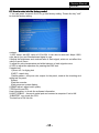
In this menu,you can adjust the picture options,
such as contrast, brightness, etc.
Press
to select, press OK to adjust.
TV
Picture
Audio
Setup
Picture Mode
Contrast
Brightness
Sharpness
Tint
Color
Color Temperature
Advaced Video
Note:
1) Audio language is available in ATSC/TVmode only.
2) Auto volume is available only when the input signal
volume is too large or there is distortion.
Energy Saving
50
50
50
50
50
3. SETUP menu
In this menu, you can adjust the Menu language,
Closed Caption, adjust the sleep timer, time zone,
Restore Default, etc.
Press
to select, press OK to adjust.
Lock
TV
MENU Back
Move
OK
ENTER
Picture
Note:
1) If you want to adjust contrast, brightness, color, and
sharpness, the picture mode will be set to user.
2) Adjust the color tempertaure to Cool to give the white colors
a blue tint, Normal to give the white colors a neutral tint, Warm
to give the white colors a red tint.
Energy Saving picture mode is the default setting, if you select
some other options, the power consumption may change.
Audio
Setup
English
Menu Language
Closed Caption
Steep Timer
Time Zone
DST
Time Format
Clock
Restor Default
Software Update
off
Pacific
off
12-hour
Lock
MENU Back
Move
OK
ENTER
3.1 Closed Caption
1.1 VGA Setting
When a PC is connected, you can adjust the VGA settings.
1) H-Pos: Adjust the horizontal position of the screen.
2) V-Pos: Adjust the vertical position of the screen.
3) Clock: Fine tune the screen width.
4) Phase: Fine tune the phase of the screen. Usually you
don't adjust this item.
5) Auto: Auto adjust to fit the screen.
CC Mode
CC On
Basic Selection CC1
Advanced Selection Servicel
Option
OK
VGA Setting
H-Pos
50
V-Pos
38
Clock
50
Phase
17
1) CC Mode: Switch the closed caption mode.
2) Advanced selection: only available in ATSC.
3) Option: Used to edit the CC font.
Note:
1) Restore Default: Restore Default will clear all the
saved channels and reset all of the settings to the
factory default values.
Auto
OK
Cancel
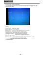
2.AUDIO menu
In this menu, you can ajust the sound options.
Press
to select, press OK to adjust.
TV
Picture
Audio
Setup
Sound Mode
Bass
Treble
Balance
MTS
Digital Output
Surround Sound
Audio Only
Auto Volume
Standard
50
50
50
Stereo
RAW
Off
Off
Off
Lock
MENU Back
Move
OK
ENTER
- 32 -
OPERATION
4.LOCK MENU
In this menu, you can change the password and adjust
the vchip settings.
Enter the password, to enter the lock menu. The
factory default password is 0000.
TV
-----
Setup
2) MPAA: Switching the movie-rating control level;
N/A, G, PG, PG-13, R, NC-17, X.
Enter Password
OK
Rating
Picture
Audio
And use the OK key to lock/unlock Parental
Controls .
System Lock
US
Canada
RRT Setting
Reset RRT
Change Password
G
PG
Age PG-13
Lock
MENU Back
Move
OK
ENTER
4.1 Change Password
1)Old password: Input the old password.
2)New password: Input the new password.
3)Confirm password: Input the new password again.
4.2 System Lock
When the System Lock switch is ON, the options
listed below can be adjusted.
4.3 US
Press OK to display the following screen.
R
NC-17
X
Description
General audiences, All Ages admitted
Parental Guidance suggested. Some material may not be
Suitable for children.
Parents strongly cautioned. Some material .may be
Inappropriate for children under 13.
Restrict. Under 17 requires accompanying parent or adult
guardian(age varies in some jurisdictions)
No one 17 and under admitted.
X is an older rating that is unified with NC-17 but may be
encoded in the data of older movies.
4.4 Canada
Press OK , to display the following screen.
Canada
Canada Eng
Canada Fre
US
TV
MPAA
OK
OK
1) Canada English: Switching the English rating control
level: EXEMPT, C, C8+, G, PG, 14+, 18+.
1) TV: Press OK display the following screen.
TV RATING
ALL
FV
V
S
L
D
OK
- 33 -
OPERATION
Description
Rating
TV
E
C
C8+
G
Age PG
14+
18+
Exempt: Includes news, sports, documents and other information
programming: talk shows, music videos, and variety programming.
Children: Intended for younger children under the age of 8 years.
Pays careful attention to themes that could threaten their sense of
securityand well-being.
Children over 8 years old: Contains no portrayal of violence as the
preferred, acceptable, or only way to resolve conflict; nor encourage
children to imitate dangerous acts which they may see on the screen .
General: Considered acceptable for all age groups, Appropriate
viewing for the entire family, contains very little violence, physical,
verbal or emotional.
Parental Guidance: Intended for a general audience, but may not be
suitable for younger children (under the age of 8) because it could
contain controversial themes or issues.
Over 14 Years: Could contain themes where violence is one of the
dominant elements of the storyline But it must be integral to the
devel opment of plot or character. Language usage could be profane
and nudity , present within the context of theme.
Adults: Intended for viewers 18 years and older and might contain
depictions of violence, which while related to the development of
plot, character or themes, are intended for adult viewing. Could
contain graphic language and portrayals of secretary and nudity.
Picture
Audio
Cable
Air/Cable
Auto Scan
Favorite
Show/Hide
DTV Signal
e-Manual
Setup
Lock
MENU Back
Move
OK
ENTER
5.1 Air/Cable:
Select Air TV signal or cable TV signal.
5.2 Channel Scan:
If it's the first time you use the TV, you should scan all
the TV channels first.
Press OK to confirm and to display the following
screen.
Air/Cable
Channel Scan
Cable
TV
Enter
Picture
Audio
2) Canada French: Switching the French-rating control
level: E, G, 8ANS+, 13 ANS+, 16ANS+, 18ANS+.
Setup
Favorite
Show/Hide
DTV Signal
e-Manual
Lock
Rating
MENU Back
Description
E
Exempt programming
G
General :All ages and children, contains minimal direct violence,
but may be integrated into the plot in a humorous or unrealistic
manner .
8ans+
Age
13ans+
OK
ENTER
Status Scanning
Analog Channels:
0
Digital Channels:
0
General but inadvisable for young children :May be viewed by a
wide public audience, but could contain scenes disturbing to
children under 8 who cannot distinguish between imaginary and
real situations. Recommended for viewing with paren.
Over 13 years: Could contain scenes of frequent violent scenes
and in tense violence.
Move
5 %...
MENU
16ans+ Over 16 years: Could contain frequent violent scenes and violence.
18ans+ Over 18 years: Only for adult viewing. Could contain frequent
violent scenes and extreme violence.
4.5 RRT setting
In ATSC digital TV mode, it can be adjusted
4.6 Reset RRT:
Press OK to reset the RRT settings to the factory
default values.
5. TV MENU
In this menu, you can adjust digital and analog TV
Channels.
Press
to select, press OK to adjust.
- 34 -
5.3 Favorite:
Press OK to choose/delete favorite channels.
5.4 Show/Hide
Press OK to display/ hide the current channel.
5.5 DTV signal
Display the DTV signal strength . It can't be selected or
adjusted.
5.6 e-Manual
The use of user guide
Service Manual
Model No.:
8.1 How to enter into the factory model
1. You can press "source-2-5-8-0" to go into factory setting. Presse the key "exit"
to shut the factory setting.
content:
1: ADC setup: set ADC value of YUV,VGA. It can also be auto-set. Adopt 100%
color bar to yuv and Checkerboard signal to vga.
2:Adjust the brightness and contrast ratio of each signal, which do not affect the
value of user's menu.
3: adjust the color temperature and white balance of each signal source.
4: SSC to adjust the spectrum for passing the EMC test.
5:special set
1)2hour off-- for Aging test
2)WDT --watch dog
3)white pattern --set pure color output for the panel, used at the checking and
aging test for panel.
4)reset
5)set the recorder
6)set power-on screen display.
6:QMAP adjust :adjust color quality.
7:PEQ set sound EQ
8:sw information: to check the sofeware information
9:UART DEBUG : Access to serial port and connect a computer if set to HK.
10:BMTEST :cpu check the CPU
The last line is SW Ver.No
- 35 -
Service Manual
Model No.:
8.2 How to update software
Haier MSD3393 F/W upgrade with USB SOP
Step 1: Ready for F/W Upgrade
1.1 Prepare a USB memory .
&RS\WKHVRIWZDUH¿OHPHUJELQIURP\RXUFRPSXWHUWRWKH86%PHPRU\DQGUHPRYH
it from computer’s USB port!
Step 2: F/W Upgrade
2.1 AC ON
2.2,then input USB , press "MENU" and choose "update software", and then press "OK".
2.3,Now you should choose "Yes",TV begin to update.You should reset TV after update.
Note: When Upgrade on the process, please don’t Power-Off!
- 38-
Service Manual
Model No.:
8.3 How to enter into the hotel model
1. You can press "source-1-0-0-1" to go into the hotel model. Presse the key "exit"
to shut the hotel model.
Content:
1.Hotel Mode: Hotel mode switch
2.Panel Key Lock: Panel key lock
3.Max Volume: Hotel mode can adjust the maximum volume
4.Start Source: Hotel mode locking TV signal source
5.Start Channel: Hotel mode locking program channels
6.Start Menu Display: Hotel Mode menu is displayed
7.Input Source Change: Hotel mode is to display the Source
8.Save to USB: TV related equipment will be copied to the system, U disk ,
to other machines used for cloning
9.Loaking: U disk data will be cloned into the machine
10.Volume Default
- 37 -
Service Manual
Model No.:
9. Trouble shooting
9-1. Simple check
- 38 -
Change LVDS wire
Yes
Check if there is +12V at
Pin35 in J1
Yes
Check if there is +30V
at C931
No picture but
have sound
No
Still having
problems
- 39 -
the
No
Change Panel
Check if Q103 ǃ
D9 ǃD10 ǃ
R700 is
working
Yes
Check if U5: Pin2(0.72V)ǃ
Pin3˄5V˅ǃPin4(12V)ǃ
Pin6(5.7V) is normal
Replace
QD6
No
9-2. Main board failure check
No
Replace
Q103ǃD9 ǃD10
Replace U5
Model No.:
Service Manual
No
Still having problems
Check the speakers
No
No
No
No
- 40 -
No
Change CD109,CD110.
Change UD10
Change LD3
Change U702
check the signal input
circuit of C710, C745.
Check the input source
Change Mainboard
Check if there is output at Pin1ǃPin4 of J17.
Yes
Check if there is input at Pin1 ǃPin9 of UD10
and check if there is output at Pin4ǃ
Pin6 of UD10
Yes
Check if there is +12V at Pin7 of UD10
Yes
Check if there is +5V at Pin3, Pin5 and Pin8 of U702
Yes
Check if there is signal at C710 and C745
Yes
Check if there is
sound input signal
No sound but have picture
Model No.:
Service Manual
Change
Mainboard
Yes
Check if the voltage
pressure of JP7 Pin2 is high
voltage pressure (More
than 3V)
Yes
Check if there is voltage
pressure in the pad of the
L806˄12V˅ˈL2˄5V˅
No sound No picture
- 41 -
No
No
Change U1
CHANGE
Q810
Replace
Remote
Control Board
other:
can' t control
Yes
No
No
Chang
U1
Yes
- 42 -
Connect the
power cord to the
socket
Still having
problems
No
Change
Mainboard
Chang UD9 or UD7 or UD8
or Q2.
Replace D806 or
U2
Check if LD23ஂ1.15Vஃଞ
LD21ஂ1.8VஃଞLD22ஂ
3.3Vஃଞ FB2ஂ3.3Vஃis
working
Check if there is voltage
pressure in JP3(12V) ଞ
JP7 Pin1(5Vstb)
Yes
Check if the power cord
is correctly connected
No sound No picture No light
No
Change sound system
Still having
problems
- 43 -
Update the software and
make the reboot;
or change the
Mainboard
For ease of use, recommend that customer format the picture and sound
settings in the automatic option.
Verify if sound system is
correct .
Poor sound
Poor sound
Still having
problems
Refer to relative
instructions in the
Manual for color adjust
Yes
check out of picture
and sound system
Yes
Verify if the same
problem exists in
other channels
No color for some
channel program (black
and white)
Change the channel to the right
sound system (PAL-M/N NTSC-M)
Check out of picture and sound
system of this channel
- 44 -
Updata the software and
make the reboot;
or change the maiboard
No
No
No color for some channel program (black and white)
Still having
problems
Check JP3 voltage of 12V
and JP8 of 5V
Yes
Check if there is high
level (2.5V-5.0V) at
Pin2 in JP7
Yes
Power on and check if
5V standby on the
Pin1 in JP7 exists ?
Yes
Check if the power cord
connect well?
Replace Q806 or Q809
Replace U1
Check if the break in the power
circuit and U2 ?
Reconnect the power cord with
the outlet to Power board.
- 45 -
Check if Main board / LVDS wire / Panel are
in good condition ?
No
No
No
No
How to know whether the Power board is broken?
1.Verify if the power cord connect well?
2.check if the power supply if working normally ; check if the power supply of
+5Vstandby is working normally;
3. check if the POWER ON/OFF voltage is high pressure;
4.check if the power supply have +12V/+5V output;
5.Check if Main board / LVDS wire / Panel are in good condition ?
- 46 -
Power board not work
1. check if the voltage input and output of boost IC is working normally.
2.Verify if the Mainboard output the right On/Off signal to power board.
3.Verify if the Mainboard output the LVDS singalto panel T-con board.
4.Verify if the software is the right version of this model.
5.Change the LVDS wire to check if it’s broken.
Panel not work
1.check if the power supply have 12V and 5V output.
2.Verify if the DC/DC convertors have the right output (5V,3.3V,1.8V,1.15V).
3.Verify if the Mainchip(MSD3393LU), AudioAMP…solder well;
4.Verify if the FLASH(U18) has the right software and work well;
5.Verify if the Y1(Crystal) has the right frequency
3. Other problem
Mainboardnot work
Service Manual
Model No.:
9-3. Pannel failure
Failure Mode
Part
Name
Description
V B/D
Vertical bar
V Dim
Vertal gray line
V L/D
Vertical color
line(light or dark
forever)
H B/D
Horizontal bar
H Dim
Horizontal gary
line
H L/D
Horizontal
line(light or dark
forever)
TCP
Phenomena
- 48 -
Failure cause
Block Defect :TCP cracking or cracking
Dim or L/D :TCP Sunken
:TCP lead cracking
:ACF bonding short
:Awful environment and
something electric enter
into LCD
:Mis-align between TCP and
Panel
:Panel failure
:TCP failure
Service Manual
Model No.:
Part
Name
Description
Phenomena
Dot Defect
Bright dot dark dot in
pannel
Failure cause
Incoming Inspection
Standard
Bladder between Polarizer
and top glass
Polarizer Bubble
Bladder in Polarizer
Panel or
Polarlzer
Tine or rigidity arose
Polarizer Scratch Polarizer Scratch
Eyewinker inside Polarizer
F / M i n s i d e Eyewinker inside
Polarizer
Polarizer
Abnormal Display Abnormal Display
Circuit
Flashing
Bright and dark
display alternately
- 49 -
1.Chip lose action
2.IC ahort or jointiog bad
3.Pannel and vsc connect
bad
Service Manual
Model No.:
Failure Mode
Part
Name
White Screen
Description
Phenomena
B/L normal,
only white screen
display
Black Screen
B/L normal,
only Black screen
display
FIIcker
Crosstalk
Failure cause
Maybe caused
by surge current
and EDS
LCD
Vcom imbalance
Circuit
Abnormal Color
Abnormal Color
Only
color abormal
Capacitance
improper bring
crosstalk inside
LCD pannel
Only
color abnormal
- 50 -
1.Chip
lose action
2.IC short or
jointion bad
3.Pannel and vsc
connect bad
Service Manual
Model No.:
Failure Mode
Part
Name
Mechanlcal
Nolse
Description
Phenomena
When
turn panel,appear
cacophony
Ripple
Connectric circle
B/L off
B/L lose action
*Connect
badness
between wire and
electrode
B/L dark
B/L brightness
darker than
normal
*Connect
badnessShort
between wire and
electrode
B/L
wire damaged
B/L
wire damaged
B/L wire open
Without backlight
B/L shut down
B/L shutdown in
sometime
F/M
F/M
inB/L ,white,balck
Rotundity
or wirelike
Operation
abnormal
or systemic noise
Operation
abnormal
or systemic noise
Short bitween
lamp housing and
wire, Because
consume power
too much
F/M in B/L unit
- 51 -
Failure cause
Caused
by Mechanica
noise of backlight
unit
Causeed by
between
mechanism and
pannel
Service Manual
Model No.:
Failure Mode
Part
Name
Light leakage
Mechanlcal or B/
L
Uniformity
Mount hole
Description
Phenomena
Brightness
at bottom of LCM
brighter
than normal
Failure cause
B/L unit badness
B/L brightness
asymmetric
Sheet in B/L unit
is uneven
Lack screw
or screw damage
*Lack screw
Screw damage
- 52 -
Sincere Forever
Haier Group
Haier Industrial Park, No.1, Haier Road
266101, Qingdao, China
http://www.haier.com
Printed in China