1
SHARP
SERVICE MANUAL
PDSMX81013-MZ
ft'
In I l l . In
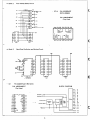
RS-232C
Serial Interface Card
•.••
,
"
" ...... , .... ~ .. ~I .......
MZ-SBI03
GP-IB Interface Card
MZ-SBI04
)
FEATURES
MZ·8BI03
• A serial interface card for MZ·80B. capable of converting parallel 8-bits data to serial data to
transmit and receive.
• Integrating two channeis of interface conforming to RS·232C (JIS·C·6361) into one board.
• Employment of Z·80SI0/0. one of Z·80 famiiy, enabling to deal with various interrupts.
MZ·8BI04
• GP·IB interface card for MZ·80B, capable of freely controlling measuring instrument groups
conforming to I EC standards ~ ~E-488 and enabling low cost, automatic measuring system.
• Capable of programming by improved BASIC .
..
....................................................................
~~
SHARP CORPORATION
~-------Contents-------MZ·8BI03
Specifications................................................. 1
General information . . . . . . . . . . . . . . . . . . . . . . . . . . . . . . . . . • . . . • . . . . . . . 2
Description of circuit . . . . . . . . . . . . . . . . . . . . . . . . . . . . . . . • . . . . . . . . . . . . 3
Troubleshooting. . . . . . . . . . . . . . . . . . . . . . . . . . . . . . . . • . . . . . . . . . . • . . .. 8
Test program . . . . . . . . . . . . . . . . . . . . . . . . . . . . . . . . . . . . . . . . . . . . . . . . . . 10
PWB and circuit diagram . . . . . . . . . . . . . . . . . . . . . . . . . . . . . . . . . . . . . . . . . . 15
MZ-BBI04 Specifications . . . . . . . . . . . . . . . . . . . . . . . . . . . . . . . . . . . . . . . . . . . . . . . . . 18
Description of circuit . . . . . . . . . . . . . . . . . . . . . . . . . . . . . . . . • . . . . • • • . . . • 19
Troubleshooting . . . . . . . . . . . . . . . . . . . . . . . . . . . . . . • . . . . . • . . . . . . . . • . . 23
PWB and circuit diagram . . . . . . . . . . . . . . . . . . . . . . . . • . . • . • . . . . • . . . . . . . 27
Packing method . . . . . . . . . . . . . . . . . . . . . . . . '. . . . . . . . . . . . . . . . • . • . . . . • . . . • • . . . . 30
Replacement parts list . . . . . . . . . . . . . . . . . . . . . . . . . . . . . . . . . . . . . . . . . . . • . . . . . • • . . 31
<.
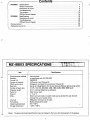
MZ:..8BI03:.SPECIFICATIONS ,~,~,
Specifications
Item
f
"
Communication me'thod
Standard
Control LSI
Number of channels
20mA current loop
Baud rate
Number of baud rates
Character length
Parity bit
Stop bit
Mode
Interrupt
Port address
Operating temperature
Storage temperature
(Note)
Asynchronous
In compliance with EIA RS·232C
Z·80SIO/0
2 (Channel A and Channel B)
Changeover is allowed for orie channel (Channel B)
Can be set independently for the two channels (Manual setting using switch)
10(75,110, 150,300,600, 1200, 1800,2400,4800, 9600 baud)
5, 6, 7 or 8 bits (Selection by software)
Odd, none or even .
1, 1Y. or 2
Either terminal mode or modem mode can be selected for ellch channel
(through the use of jumper chip).
Z·80 vector interrupt can be used.
,
Manual setting with switch
O°C- 50°C
-25°C- 80°C
'
..
The above·mentioned specifications may be changed ir, the future for improvement of the product.
r
"
• Introduction
Ther~ are two methods of data communication between computer and external equipment: S-bit parallel and
bit serial.
The serial interface card MZ-SBI03 (hereinafter referred to as "interface ~ard") permits data communication by the
bit serial method. This interface card is manufactured in accordance with EIA RS-232C (the Electronic Industries
Association RS-232t::), and used for data communication with other equipment having interface based on RS-232C.
• Functions of this interface card
The interface card has the following functions.
1. One card has two channels, each of which is capable of transmitting/receiving data independently.
2. One of the ten baud rates can be selected by operating the switch on the card. Baud rates can be set independently
for the two channels.
3. Output connector signals to external equipment can be in either terminal mode or modem mode through the
operation of the jumper chip.
4. This interface card can be used as 20mA current loop for one channel.
• Applications
)
Equipped with the above-mentioned functions, the interface card has a variety of applications. Some applications of
this very versatile serial interface card are shown below.
1. Data communication between computers on telephone line via acoustic couplers
2. Printer
3. Plotter
4. Digitizer
5. Color display
6. Card reader
7. Magnetic tape equipment
.
\
)
•
2
W
)
Bus
+5V~
Power
Supply
Circuit
Add'~~
..
H
-12V
['m
furt
Address Select
Circuit
q
~~
Co"",,' ••'
D....
I
BR1
BR2
DCDA
14
DTRA I
CTSA
RTSA
RxDA
TxDA
H~~'Cb
DCDB I
CTSB
Rml
DTRB
RxDB
TxDB
.~
RS-232CI
Channel B
Baud Rate Setting (SW-31
~
-)
v
Chlnnel A
Baud Rate Setting (SW-21
(J-2)
Current Loop
Select
~
./
RS-232C
Drive
RS-232C
Drive
Current
Loop
Drive
..
)
./
~
~
~
Blud Rate
Oscillltion
Circuit
(J-3)
Mode
Select
(J-1)
Mode
Select
Channel A
Connector
Channel B
Connector
&.
3
Cl)
~
ca
0
;+
c
n
~
•
n
Z.
:-
"-
0
',"~
r·._
'C
.
.:\
f~";
t',
v..;..#
.~;~";
~
-
c:
0
I:D
0
• '.""',.1-,.
.
-....
"
0-
:D
0
en
C
m
CA)
0
e
ex»
I
3::
N
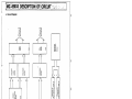
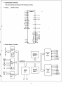
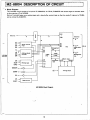
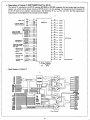
• Construction of Circuit
The serial interface card consists ?f the following six blocks.
•
Block 1
Hybrid IC circuit
D'
D'
01
••
HOOO2PA
D.
...,.
...,.
D'
D'
01
....
D'
00
IhO'
Cl
It" •
1111
.1JII1i
"TI'
rntI
•
•
In
1t11'T
C'I'I
CTITI
A'
AD
r
'1'
'1'
.10
'10
rnn
• RT1il
DTItI
..
DCDI
••
.,.0 ....
IY"CI
,.DA
•• 0&
..
.
DT.'
DCOI
N.C
N.C
H
It'l.
'hO&
ItTI"
CITA
CSTA
DT ••
0'"''
DCD"
DCO'
.,,,oYA
+.v
'IDA
'''''CA
)
IND
U.
•
•••
U.
Block Diagram of Hybrid IC
0,
D.
0,
D.
0,
O2
)
D.
Do
<:>
Data BUI
Driver
~
0
Ml
CE
RESET
Bus
Interface
Logic
fG:
~
A.
AD
D
IEI
IEO
)
~
Channel A
Data
&
Control
Channel B
Read/Write
Registers
DCDA
SYNCA
U
U
RTSA
CTSA
DTRA
W/RDYA
lr
Intetnal Bus
Internal
Control
Logic
ExlNT
RxDA
Channel A
Read/Writa
.Reglsters
IORO
RD
TxDA
..
TxDB
RxDB
RTSB
~
Channel B
Data
&
Control
CTSB
DTRB
DCDB
W/RDYB
I!"terrupt
~
Control
Logic
SYNCA
"-r-BRl
BR2
I
4
•
Block 2
Port Address Select Circuit
..
le4
LS2&'h2
147
IC3,4
+5V
I.
A.
I e4
A'
I e4
144
(
RH·iX0190PAZZ
(SN74LS266N)
PIN ASSIGNMENT
(Top View)
le4
145
le5
142
le 5
CE
.SV
(
5.51\"6
RA I
SW-I
•
Block 3
Baud Rate Oscillation and Setting Circuit
1A2
R~OK
10
.SV'-~""'+'"
c
REiE'f
B
II
I .••JI ....
+'V _ _ _---='.::j4
..
ICl
c
sw-z
IC I
MCI4411
IBI
RH·iX0297PAZZ (MC144ll)
BLOCK DIAGRAM
PIN ASSIGNMENT
(Top View)
Fl
11
Rite Sllect A 23
24
2
3
22
4
21
6
RI.I Select 8 22
23
20
19
18
I
.1
Cryltlljn 21
•"
Divide ...
Rill
Select
LotiC
Cryltl1o..n: 20
f2
2
F3
16
F4
3
F5
15
f6
4
F7
5
7
F9
F8
e
Fl0
Fll
8
17
8
14
9
16
13
FI3
10
15
11
F14
11
14
12
13
18
F16
19
F16
R.Mt
10
5
f12
C
,
•
Driver, Jumper, Switch and Connector Circuit
Block 4
+1
./-1
... ~.sf
)
1
L.. _ _
~
T.
+IIV"
Ic2
TIDI _ _ _ _-.J
,
1 ,....---...,
It.~
.,.
-
751 . . "
'<1
t _000~-iI--+-...:cO)(.~c:
I ..
It. 01
ItTlI
o~
----=.~~..,..I'-----...
-Y.:,
--,
-~
I
.
I
.~~~.;..-.__. .
i
CTII
I
..
'.0
OTltl _ _ _ _-.I
+IIV
IC'
•
)
6
C1
l··o'
OTIt~-9-~'
'--r-...J
,-- - -...,
.
--'
.
'
-IIV
51
..
••
2.'111
on
••u •
'OO
IC2
DCDI
~
I··""
-IIV
"I'A
------c~1< ..
-'1----...
+IZV
.10
r!>
100
Cl
T .DA _ _-:..,:...
)
CH"NNEL-I
CHANNEL-A
./-1
~~II
I
ICI
,..
~...
•
ItTIA _ _
:.
...r~-M
-'L""1....
L._, __ •
- : . . . , - - - - - - - - - - - - - - -....
7511. . 21
,
It.OA ----_.....c~;.c:- .10_ _ _...
I
~
'
ca.
--It!.l~ :I; ••01'
~C 7
I" -
'1--.'. .___________~~
~t::f-j------------------~@
~i~IIA
4r~1
: ~'. L._ , __ •
:I
CSTA
)
'" ..
I
DTltA _ _ _
DCDA
,. c ••
.~.~II::
~
01'
~'is~1A
:
'[~
'L_ j==~...,-,---------------r®8
-----....:.·OM~.
~
-
Iml'
• IC2, 8
RH·iX0305PAZZ
(SN75189A)
• IC7,8
CONT·
ROL
4A
1
PIN ASSIGNMENT
(Top View)
4
4V
11
RH·iX0085PAZZ
(SN75188N)
PiN ASSIGNMENT
(Top View)
Vcc+ 48
1
38
)
5
1A
1
1V 2A
CONT·
ROL
2
2V GND
CONT·
ROL
Vcc- 1A 1V 2A 28 2V GND
6
•
Block 5
Power Supply Circuit
c
LI
eH'"
+ IV
+IIV
ce
I~/.
aND
aND
cia
-IIV
U~
GND
(
r
. IC13
,
DUNTK0064PAZZ
(12N10K1)
~
1. GND
2. Vi"
3. V out
LA1---V
•
Block 6
4.
c
N.C
Bus Interface Circuit
c
.
..
c
~------------------------------------------------------------------------~
7
The serial interface card consists of six blocks and, if each block functions normally, a faulty operation is caused by an
external factor (Ex: program, the counterpart machine, etc.) •
.. .
• Circuit Blocks and Check of Behavior
Block
Behavior
Circuit
1
Hybrid
Z-80SIO is built in and te~t the function by the test program.
2
Port address
selector·
Check if an address code set by SW-1 (DIP switch) is output.
If the output does not agree, wired-or output is a low level.
3
Borate
oscillation
and setting
Check if MC14411 is outputting.
r - - Frequencies are as follows:
....
..
..
F1 .. 153.6 KHz
F3
76.8 KHz
F5
38.4 KHz
F6
28.8 KHz
F7
19.2 KHz
F8 • 9,600 Hz
F9 .. 4,800 Hz
F11 .. 2,400 Hz
F13· 1,758.8 Hz
F14· 1,200 Hz
Be sure that two or more switches of SW-2 and SW-3 (DIP switch) are not turned
on. Tolerable deviations are ±0.1% for each frequency.
In measurement, consider that the waveform of MC14411 varies according to
the load capacity because MC14411 is CMOS.
4
5
Drivers,
jumpers,
switches and
connectors
Power supply
• 5V line
• +12V line
• -12V line
6
Bus interface
Check the status of input signal.
High level: -10V to .... 12V
• Output of 75188 }
Low level: 10V to 12V
Input of 75189
Ci9h: OV to 0.8V)
Input of 75188 }
TTL level
Output of 75189
Low: 2.5V to 5V
If reset, the output terminal of the hybrid IC is in the high level (high level of
TTL level).
-
•
•
Be sure that the voltage is +5V ± 5%.
Be sure that the oulput of DC-DC converter is:
+12V ±lO%, -12V ±10%
0
Since there is no circuit part, examine if the signal is input to the board
normally.
The hybrid IC is not actuated unless the clock signal is applied to the q, terminal
of the hybrid I C.
8
-.
-
• Faulty symptoms and connected circuit blocks
Circuit blocks
1
2
0
0
3
4
5
6
0
0
Faulty symptoms
and probable causes
0
0
0
3
o
•
4
5
0
0
c
Faulty 'symptoms
and probable causes
6
+12V or -12V line deviates
over ±10%.
(Causes)
o Faulty TL497 AC.
o Faulty 12N10K1.
o Short circuited load.
o Short circuited electrolytic
capacitor.
• Other.
o
(
Othe~.
Error message is generated from Z·80SIO
(parity error, overrun
error, framing error,
etc.)
(Causes)
o Wrong borate setting.
o Abnormal borate
oscillator.
o Wrong jumper setting (J-1,J-2 and J-3)
o Abnormal +12V or
-12V line.
o Faulty connector.
o Faulty counterpart
machine.
o Other.
0
0
2
Transmission buffer
is not empty.
o Control does not
return from the
transmission routine
in test program run.
(Causes)
o Hybrid IC doesn't
function normally.
o!p clock is inoperative.
o Wrong port address
selection.
• Abnormal 5V power
supply.
.
0
1
o
o
0
Circuit blocks
0
,0
•
Borate oscillator does not
output.
(Causes)
o Faulty MC14411.
o Faulty crystal.
o Two or more dip switches
(SW-2, SW-3) turned on.
o Faulty borate clock input
circuit of hybrid IC.
o Other.
(
c
• Signal is not input.
o Control does not return
from input routine in
test program run.
(Causes)
o Wrong borate setting.
o Abnormal borate
oscillator.
o Abnormal +12V or
-12V line.
o Wrong jumper setting
(J-1, J-2 and J-3)
o Faulty connector.
o Faulty opel'1ltion of
hybrid IC.
o FaUlty counterpart
machine.
• Faulty driver IC.
o Other.
,
,
(
.. 0" shows a related circuit.
.. 0" shows a related circuit .
9
MZ-SBI03 TEST PROGRAM
• Self-diagnosis program
Let ~s consider a program for self-diagnosis of this interface card and assume that data are transmitted
from Channel A are reCeived by Channel A. For channel B, similar communication system shall be adopted. Self·
diagnosis of the interface card can be made by examining whether the reoei.e data and transmit data are the same at
the time of transmission/receiving.
• Setting jumper blocks on the card
For'the self-diagnosis as mentioned above, set the jumper blocks on the card as follows.
J-2
J-l
T
M
R
C
I,
J-3
C
M
T
0
0
0
0
0
0
0
0
0
0
0
0
0
0
0
0
0
0
0
0
0
0
0
0
0
0
0
0
0
0
0
0
0
0
0···1
0
0
0
0
0
0
0-
0
0
0
0
0
0
0
0
0
0
,I
0
III
0
Since port addresses BOH, B' H, B2H and B3H are used in the program, set the switch SW-' in the following (factory
setting).
Switch segment
6
5
Switch position
OFF
ON
,
•
4
3
2
1
OFF
OFF
ON
ON
Set the switch for baud rate setting as desired. After setting each mode, install the card in MZ-aOB. On this occasion, signal cable needs not to be connected.
L_'_ _ _ _ _ _,
10
• Flow Chart of Self-diagnosis Program
Start testing Channel A. Stop the program when an error occurs. If Channel A is found normal, test Channel B then.
Set Z80-SIO
mode
Start checking
Channel B
Start checking
Channel A
"
Output test data
from Channel A
Contantl of arror
displayed
Output tast data
from Channel B
Contents or error
displayed
No
No
.....---<
Channel B is
normal
------ _ _--...
-------.
11
-----
-........--..-...
• Program by BASIC language
.,
Now, let us draw up th~ program described in the above·mentioned flow chart, using tBASIC languages. The
program list is shown later.
In the BASIC program, the routine to control the interface card is composed of machine language. The machine
language data are w.ritten into the memory by POKE statement and the routine is called by USR statement. The
routine is made by programming statement Nos. 1000 through 1990.
.. .
Statement Nos. 1080 -- 1160........... Parameters
Clock rate
Stop bit
Parity
Odd/even of parity
Transmit/receive character
Auto enable
16
2 bits
Present
Even
8 bits
Set
:·X
Statement Nos. 1180"" 1370.•.........Mode setting routine.
Statement Nos. 1550 -- 1610...........Channel A input routine.
Input data are stored in Address CHAR.
Error flags are stored in Address INER@.
Statement Nos. 1630 -- 1740. . . . . . . . . . .Channel B input routine.
Input data are stored in Address CAHR.
Error flags are stored in Address INER@.
Statement Nos. 1780 -- 1840...........Channel A output routine.
Transmit data are stored in Address CHAR.
Statement Nos. 1860 -- 1930...........Channel B output routine.
Transmit data are stored in Address CHAR.
Statement Nos. 1950 -- 1990...........Writes machine language data in the memory.
tBASIC Version: SB-6510, SB-5510
,
•
17
~--------------------------------------------------------------~
13
)
1630
1640
1650
1660
1670
1680
1690
1700
1710
1720
1730
1740
1750
1760
1770
1780
1790
1800
1810
1820
1830
1840
18S0
1860
1870
1880
1890
1900
1910
1920
1930
1940
1950
1960
1965
1970
1980
1990
3000
3010
3020
3030
3040
30S0
3060
3070
3080
3090
3100
3110
3120
3130
3140
3150
3160
3170
3180
3190
3200
3210
3220
3230
3240
3250
3260
REM CH9IN ENT
; [ adr.='F04A ]
REM
IN A, (CH9CT>
:DATA DB,93
REM
R'RCA
:DATA OF
.JR
REM
NC,CH9IN :DATA 30,FB
REM
A,I
LD
IDATA 3E,01
REM
OUT
(CHBCT> , A :DATA D3,B3
REM
A,(CHBCT) :DATA D9,B3
IN
:DATA E6,70 ••
REM
AND
70H
(INER@),A :DATA 32,32',FO
REM
LD
REM
IN
A'( CHBDT> IDATA D9,B2 '
(C.HAR) , A :DATA 32,33,FO
REM
LD
REM
RET
:DATA C9
REM
REM *** OUTPUT ROUTINE ***
REM
REM CHAOUT ENT
[ adr.=SF060 ]
A, (CHACT> IDATA DB,91
REM
IN
2,A
REM
9IT
:DATA CB,S7
REM
JR
Z,CHAOUT IDATA 28,FA
A,(CHAR) IDATA 3A,33,FO
REM
LD
(CHADT> , A :DATA D3,BO
REM
OUT
REM
RET
IDATA C9
REM
I [ adr .... F06C ]
REM CH90UT ENT
A, (CHBCT> :DATA DB,B3
REM
IN
2,A
:DATA CB,S7
REM
BIT
Z,CHBOUT :DATA 28,FA
REM
JR
A,(CHAR) :DATA 3A,33,FO
REM
LD
(CHBDT> , A :DATA D3,B2
REM
OUT
REM
RET
IDATA C9
REM
END
:DATA END
REM
DIM X(30)ILIMIT .FOOO IP-15*4096
FOR JaO TO 9:X(J)-JINEXTIFOR J-O TO SIX(17+J)-J+I0INEXT
PRINT"SIF SUBROUTIN LOADING"
READ X'IIF X'-"END" THEN 3000
J-16*X(ASC(MIO.(X.,I,I))-48)+X(ASC(MID.(I',2,1))-48)
POKE P,JIP=P+IIGOTO 1970
REM **************************
REM *
*
REM *
MAIN PROGRAM
*
REM *
*
REM **************************
REM
USR(.F009)IREM
mod. s.t ~,
PRINTIPRINT:PRINT "***** TEST PROGRAM (S.ri~l I/F M2-8BI03) ***** "
PRINT
PRINT "Chann.l A TEST"
FOR 1-0 TO 2SS
POKE .F033,I :USR(.F060)IPOKE .F033,O : REM chann.l-A output
USR(.F034)IA=PEEK(SF033):ER-PEEK(SF032) I REM chann.l-A input
IF ER<>O THEN PRINT"COMMUNICATION ER - ";ERISTOP
IF I<>A THEN PRINT"COMPARA ER":STOP
PRINT"."I:NEXT
PRINT"*** OK ***"
PRINT
PRINT"Chann.1 B TEST"
FOR 1-0 TO 255
POKE $F033,I:USR(.F06C):POKE .F033,O
: REM chann.I-9 output
USR(.F04A):A=PEEK(.F033):ER=PEEK(SF032) : REM chann.l-B input
IF ER<>O THEN PRINT "COMMUNICATION ER '"' ";ERISTOP
IF I<>A THEN PRINT "COMPARA ER"ISTOP
PRINT"'"; :NEXT
PRINT"*** OK ***"
END
14
A
o
c
B
E
F
H
G
•
.'" 1
~
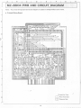
Z-SBI03
BAND
IT DIA
•
\
Notes: The printed wiring board circuit diagram are subject to change without prior notice .
•
• Printed Wiring Board
2
•
3
•
SERIAL
TERFA
•
•
+ .
CD
o
I
•
10
•
•
••
Perspective' View
--"
-,' Opposite side
11
•
•
15
•
Parts-fitted face
1
c
B
A
D
E
F
H
G
I
J
K
o
N
M
L
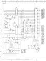
• Circuit Diagram
.,
..
2
••
AS
3
.,
,"
,"
,"
AS
..
'C 5
H
,- ,
-,
HOOQ2PA
+12'"
-r-J
~
,
I
.,
,
,
••
..
'"
,~.
"
,
Z. '
0
I
I
I
I
--
~-
~
,,~
I
, ". •
7"88 •
"
~-
'"
--
.,
r
c __
FlnlH
CTSTI
5
...
13Kx;S
• W-,
OTI'I •
. I,-0
~
-~
.,
--
,
.,.
~-
- 12V
""
'"
"'
. . .. ID
6
..
-
-
OT RII
hiNT
"
I
011
•
•
t~ . . .
u.
RTS 8
4
"
-
•
JORQ
",
."
DeDI
(ID
'"
W/ROT8
CHANN~L-'
SYNC B
7
p
H
T .OA
..''',.."
• ®
CHANNEL-A
,,
IhOA
IIlT,A
eSTA
OTA ...
"
~
DCOA
+
,
W/ROYA
.. ,
B
SYNCA
...
G ••
r
I
"
~
I
I
9
• • NO ."UORAn
.!9.
•,
,
,0
,
•
•
••
!L
"
• • 00
•
.. lOO
24 00
1.00
..
1200
,
,••
".
".
~
"
-::r-:--------::::
~-
"
I
16
to.
8.- 3
,AI
MZ-BBI03
17
•
•
.
Specifications
Item
Interface standard
In accordance with IEC Standard/TC66.
Interface funcion
Functions executable in MZ-,801rv"ersion-up BASIC language.
,
Function
Subset
Description
SH
SHl
All functions
AH
AH1
All functions
T
T6
Basic talker
Serial poll
Cancellation of talker by MLA
L
L.
Basic listener
Cancellation of listener by MTA
C
Cl
System controller
C2
IFC transmit. controller in charge
C3
REN transmit
C.
Response to SRQ
C6
Interface message transmit
Controller receive
Controller pass
Controll pass to itself
Parallel poll
SR
SRO
No function
RL
RLO
No function
PP
PPO
No function
OT
OTO
No function
DC
OCO
No function
Output connector
(Male type) connector in compliance with IEC Standard
Operating temperature
6°C"'" 35°C
Storage temperature
OOC"'" 50°C
Power source
DC 5V (supplied from MZ-80B)
•,
Reference
The following specifications are "reference" specifications. since difference is caused by cable quality. connector
connection. noise and other environmental conditions.
1. Number of Instruments per
system
15 max. including MZ-80B
2. Full length of cable per system
20m or less
However. length per instrument shall be about 2m. If the number of instruments exceed 11 in one system. cables of 2m or less shall be used between
instruments so that the full length will be 20m or less.
(Note)
The above-mentioned specifications may be changed in the future for improvement of the product.
18
IMZ-SBI04
r--
:. J
DESCRIPTION OF CIRCUIT
• Block Diagram
This interface circuit consists of a hybrid le (H0001 PAl for GP·IB, Z·80AP10 and various logics to connect them
to the extension I/O of MZ·80B.
Some of included logics are a waiting logic and a data buffer control logic so that the mode 2 interrupt of Z·80A
can be utilized by Z·80API0.
r---
....
...
DB7
tU
Data bus
8
I
8
~
ID
Dltl b us
DBO
8
8
lE 1 lE 0 M1---A0 -
Buffer control
logic
R1
W1
W2
I--
I-
07
L...,.
A7
I
A0
MZ·80B
bus line
8
A0 WR _
Address decod·
ing logic
.
IORa
--
Z·80A
PlO
MI
INT
-
l
GP·IB
5
TACS
-
3
Hind sheke
line
5
CE
Waiting logic
EXWAI T
I
DO
-
M1 - BUS4>
-
HIC
Mlnlgemlnt
line
Mlnage ment
line
LACS
8
Command
CMAC NBA
NBAW
ACCS
reed
IEO
IEI
iEi-
T
Timing circuit
lE 0
MI
RESE T
•
Reset circuit
MZ-8BI04 Block Diagram
.
..
~--------------------------------------------------------------------------------------~
19
I
• Description of Hybrid le RMPTHOO01PAZZ for GP·IB,
The hybrid IC mounted, on the GP·IB interface MZ·8BI04 of MZ·80B integrates the hand shake logic, bus driver/
receiver, etc. which are the proper circuits of GP·IB circuit, into one package. By connecting this HIC (hybrid IC)
to the I/O ports of an ordinary microcomputer, the functions of T 6 , 4, SH 1 and AHI and the inputting and
CJutputting of the l1'Ianagement line and data line are enabled.
.. .
27
DB,
Data line (
Internal register (
read/write pulse
Input to hand
shaka line and
management line
I
DB.
Wl
lIE
32
2
3
4
5
33
34
35
36
-~
9
[T ACS
LACS
SPAS
2
3B
13
4
15
39
40
10
41
49
50
51
CLR
47
Waiting time
setting
~NBAW
NBA
55
52
~ ACCS
53
54
CMAC
37
11
Reset .ignal
Waiting time
setting
31
7
-~-
EOHO)
Management ATN(O)
line output
SRO(O)
[ IFC(O)
Enabling manage. REN(O)
ment lines other ENABLE
than EOI
Reporting of
Internal logic
status
HOOO1PA
19
16
R1
W2
OAV(R)
NRFO(R)
NOAC(R)
EOUR)
ATN(R)
SRO(R)
IFC(R)
REN(R)
30
-~?g
43
44
45
0108
0107
0106
0105
0104
0103
0102
0101
GP·IB line
SRO
IFC
REN
ATN
OAV
NRFO
NOAC
46
EOI
42
11
SG
Signal groun"d
1171561~2~48
Vcc
GNO
• Block Diagram of Hybrid le'
D7
De
D5
0108
0107
0106
0105
0104
0103
0102
0101
DATA
D4
DATA LINE
D3
D2
D1
PORT
t--.-J
DO
DAV R
NRFOR
NDACR
EOI
R
ATN R
SRQ R
IFC R
REN R
rr-.......==-=-......
slgnal
~§~
GND
W2
DAV
GND(E)
CMAC
Aces
NB':
LACS
TACS
ClR
SPAS
EOI D
NRFD
NDAC
~~~~~~i~~~~~~~J
EOI
ATN
SRQ
ATND
SROD
IFC
RENO
REN
IFC D
Driver /Receiver
20
• Description of Each Circuit
Each circuit will be described. The logic diagrams used for description are simplified schemata of logic.
c
1. Reset Circuit
RESET----I
)O----~
To Pia M1
MI------'
The circuit is intended to reset PlO by the RESET signal from MZ·80B CPU board. Z-80APIO is reset when MI
terminal is active for 2 clock cycles or over providing that both "Fm and 1U"RO" signals are not active. The RC
circiut in the diagram is a low pass filter provided for preventing faulty operation d~e to noise.
2. Waiting Circuit
MI---\
IDROW
MI----i
.;xl~--<2
LD
EXWAIT
BU&/> - -
Vcc
The waiting circuit corrects the timing of the interrupt vector transmitting from PlO to CPU in the interrupt acknowledge cycle. Thus, 10RQW develops a signal of reversedlORO and EXWAIT doesn't develop pulse in other
cycle than the interrupt acknowledge cycle.
This waiting circuit does not correct the timing of the daisy chain. With the delay of the daisy chain, lED look
ahead is carried out on the extension I/O interface of MZ-80B.
The timing chart in the interrupt acknowledge cycle is illustrated below.
(
Lalt M cycle
Interrupt
detection
I
T2
Tw·
Wait line
. detection
T'i
Tw
Interrupt vector
input
c----,
-----""\ Ir------ --41- ~ -m1
.
.
EXWAIT
,)pROW
________________________________----~I
21
\'----
•
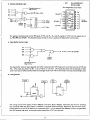
3. Addre•• Decoding Logic
A. -r---i.._
As
Vcc
to PlO ~ (COH-C3H)
A. - - < I
A, - - < 4
AH·iX0303PAZZ
SN74LS138N
Pin Assignment (Top View)
,--_ _ Decoded output of
COH to C7H
A,
ICg
YO
W, (C5H)'
WI (C4H)
ENABLE
("lA •
G28 5
~1
C
B
Ao
OUTPUT
~A~~~----. RI (C4H)
V7
6
Y1
V2
Y3
DATA
OUTPUT
V4
VS
V6
The address decoding logic forms ~ signal of PlO and A I, W I and W2 signals of H IC from the signals Ao to
A" AD, WA and 10POW. The decoded output of COH to C7H is used by the data buffer control logic.
4. Data Buffer Control Logic
IEI - - - - I
IEO -----0
MY
p---- To No. 1 pin of IC6 (LS24S1
----0
RD - - - d
IOROW
(lORO)
Decoded output of
COH to C7H
The data buffer control logic ,regulates the buffer connecting the CPU data bus line and the bus lines of PlO and
HIC. CPU reads data when the No. 1 pin of ICS is in low level. CPU reads data when the 10 addresses of COH
to C7H are input to CPU and CPU reads the interrupt vector from PlO in the mode 2 interrupt acknowledge cycle.
,
5. Timing Circuit
a
B
5/ols
The timing circuit forms pulses of about 500J,Jsec. and about 5J,Jsec. 500J,Jsec. determines the time for receiving
one command when the ATN signal is received in the slave mode and 5J,Jsec. determines the time from trans·
mitting data on to the GP·IB data bus to outputting DAV. It is so designed that 500J,Jsec. pulse is not generated
untillEI becomes high level, by considering the disposition of ATN by interrupt.
27
MZ-SBI04 TROUBLESHOOTING
BASIC (Commands other than GP·IB) does not work normally.
No
Fault of other part than GP·IB
interface.
(N): Normal, (A): Abnormal (With tha method of
intarpretation, refer to paga 25, 26.)
(N): Normal
(A)
(N)
Faulty IC12
>--~
"-
Abnormal IDROW signal
•
(N)
Abnormal EXWAIT signal
IC connected to input
line is faulty.
23
(N)
>;"""':'-.j
Faulty IC1
(A)
>;"""':'-1 Faulty IC1
BASIC works but GP·IB commands do not work.
Ves
Faulty 1C9, IC11
•,
Ves
No
Faulty address decoding
circuit (lC11, IC10and
IC3)
">N_°--lOOiCheck abnormal signal.
·1 The R EN line of GP·IB becomes low level by the command
REN and high level by the command LCL
·2 Pin @
outputs negative pulse by reading 1/0 address
C4H (1961.
Pin ([\)
outputs negative pulse by writing on to 1/0
address C4H (1961.
Pin (j)
outputs negative pulle by writing on to 1/0
address C5H (1971.
24
• Methods of Interpreting Whether Normal or Abnormal
Each terminal is normal if it is in the following status in the "READY" condition after run by BASIC.
Pin No. of IC
Normal condition
ICl
®
Negative pulse
Same as MI (CPU bus)
ICl
CID
Positive pulse
Reversed MI (CPU bus)
ICl
@
Constant L level
IC2
(j))
Positive pulse
IC2
®
Reversed buscJI
IC3
@
Constant H level
IC5
CD
Positive pulse
(Turns H level when XXCOH to XXC7H are transmitted
address bus.)
IC5
<V
Positive pulse
Reversed RD (CPU bus)
IC5
@
Positive pulse
Reversed 10RQ (CPU bus)
IC5
@
Positive pulse
Reversed MI. (CPU bus)
IC5
@
Constant L level
IC6
CD
Constant H level
IC7
@
Constant H level
IC7
@
.
Constant H level
IC7
@
Constant H level
IC7
CID
Constant H level
IC7
@
Constant H level
ICS
@
Negative pulse
Same as Mi (CPU bus)
ICS
@
Negative pulse
Same as lORQ (CPU bus)
Reversed MT (CPU bus)
Output terminals of address decoding circuit
ICll ®
•
Develops negative pulse when I/O address COH to C3H (192 to 195) are accessed.
IC9
@
Develops negative pulse when I/O address C4H (196) is read out.
ICg
QV
Develops negative pulse when data are written on to I/O address C4H (1961.
ICg
Q)
Develops negative pulse when data are written on to I/O address C5H (197).
.
~.
25
Input terminals of PlO
IC12 @
Same signal as A 1 (CPU bus)
®
Same signal as AO (CPU bus)
@
Same signal as RC (CPU bus)
@
Same signal as IORa (CPU bus)
@
Same signal as MI (CPU bus)
@
Same signal as IEI (CPU bus'
@
Same signal as BUSt/I (CPU bus)
,
In BASIC ready status
••
At transmission of data to GP·IB
At receiving data in slave mode
IC13 @
Constant L hivel
Outputs positive pulse of
about 5llsec.
Constant L level
IC13 <I}
Constant H level
Constant H level
Outputs negative pulse of
about 500llSec.
.,
26
,
A
B
o
c
E
MZ-8BI04 PWB AND CIRCUI
•
F
H
G
DIAGRAM
Notes : The printed wiring board and circuit diagram are subject to change without prior notice .
• Printed Wiring Board
2
3
4
5
,
7
•
. .'
•
Perspective View
D
8
D
•
27
Paru·flned 'ace
Opposne Side
•
:~,~ .,.,' '(;''<i1-~'::;~'~'~'~
j':~".e.: ~.::~.•>.:.:";~,'~;" ,:':.~~,,~
....
,
_.
.,',
'
-
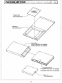
Protected Seat
(SSAKH0043PAZZ)
PWB Sleeve
(SPAKS002SPAZZ)
~--- Packing Case
(SPAKC01S5PAZZ) for MZ-SBI03
(SPAKC01S7PAZZ) for MZ-SBI04
Instruction Manual
(TiNSE0036PAZZ) English for MZ-SBI03
(TiNSE0037PAZZ) English for MZ·SBI04
' - - - - Seal x 2
(TSELF0001PAZZ)
30
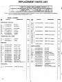
REPLACEMENT PARTS LIST
" ,i:;;'HOW;;:rO,"ORD,ER: R~,LACE~ENT:.~AFtT~~;:~;t:~~i:';~~' .;.
,:,,','
(
:T~ have you~ ~rd8r,fllled promptly end corr~ly:.~J88S1t.furnlsr tIl8 f()lI~i~.19tor.if1f9nt
'....\'~
.'.
,~" "t. '2.',·FiEF • NO'." .,,~
"
11', )(,£,.1 '.
,'
.~~',.J\
, ,,1'',. MOOE~ NAMe·~··
" .~*-(r.·~ , '.,.,.~
',; ''''.
"'.~:;
"t.. i ,;:t.~
., ~. '. , ; • ~.' l-\
. :;. .tJ:
. .~'t.' ~"
"'
't', ~;;: ~
..':~'; '~',.
l,.', !.3~,P~R!{Nq·.. t~'.,,:(· .... ~:7::~,fo";(J>.~.,}?,e~.~p,r'~~\\·· ~'I /;1S~~f,"'.:¥
.:-
NOTES; Be sure to use regular parts for securing the safety and reliability of the set. Be sure to replace these parts with specified
ones for maintaining the safety and performance of the set.
MODEL MZ·8BI03
REF.
NO.
PART NO.
DESCRIPTION
INTEGRATED CIRCUITS
ICl
IC2
IC8
IC3
IC4
IC5
IC6/'
IC7
IC9
IC13
}
}
C3
C16
AH·iX0297PAZZ
MCl4411
BA
AH·iX0305PAZZ
SN75189AN
AM
AH·iX0190PAZZ
SN74LS266N
AF
AMPTHOOO2PAZZ
Hybrid IC
BU
AH·iX0085PAZZ
SN75188N
AM
AH·iX0152PAZZ
DUNTK0064PAZZ
TL497CN
12Nl0Kl
AU
BF
}
VS2SA49&O/.1
2SA49&O
AF
VHD1S1586//1A
lS1586
AB
VAC·MT2EG 106K
10M ohm. 1/4W
AA
A2 }
A14
VAD·SC2EF102J
lK ohm. 1/4W
AA
R3 }
R15
A4
R5
VAD·SC2EF103J
10K ohm. 1/4W
AA
R6 }
Rl0
R7
RSr
R9
Rl1
A12
R13
R16
RAl
VRD·SC2EF272J
VRD·SC2EF472J
2.7K ohm. 1/4W
4.7K ohm. 1/4W
AA
AA
VRD·SC2EF101J
100 ohm. 1/4W
AA
VAD·RU2EE222J
VRD-RU2EE561J
VAD-RU2EE273J
VRD·SC2EF221 J
VAD-SC2EF561 J
VAN·RT2HCl ROF
VRD·SC2EF l04J
RMPTC10l9PAZZ
2.2K ohm. 1/4W
560 ohm. 1/4W
27K ohm. 1/4W
220 ohm. 1/4W
560 ohm. 1/4W
1 ohlfl. 1/2W
lOOK ohm. 1/4W
Resistor A.rray 3.3K ohm x 6
AA
AA
AA
AA
AA
AB
AA
AC
VCTYPU1BD104Z'
O.lMFD. 12V. Ceramic
AB
VCKZPR1HB221K
220PFD. 5OV. Ceramic
AA
(
(
C24
C8
C9
Cll
C12
C14
C18
C20
Cl0
C13
C15
C19
C21
C17
VCEAAUOJW107Y
l00MFD. 6.3V. 'Alumlnum
AB
VCKZPA1HF103?
O.OlMFD. 5OV. Ceramic
AA
VCSACU 1AE336K
33MFD. 10V. Tantalum
AD
VCEAAU 1CW336Y
33MFD. 16V. Aluminum
AB
VCCSPR1H6151J
150PFD. 5OV. Ceramic
AA
RCi LF7863VAZZ
Coil CH04
AG
RCi LF7862VAZZ
Coli CH03
AG
RCiLF7864VAZZ
RCRSAOO17PAZZ
QSW·DOOO4PAZZ
Coll8S651
Crystal 1.8432MHz
Dip Switch (6 contacts)
AK
AP
AR
QSW-DOOO6PAZZ
r
)
}
VCTYPU1BD104Z
L1
L2
L4
L3
X'TAL
SWl
SW2
SW3
J-l
J.2
J.3
}
}
}
CNl
CN2
}
Dip Switch (10 contacts)
AR
QPLGZ0103PAZZ
4-Pin Plug
AD
QPLGZ0102PAZZ
3-Pin Plug
AC
QJUM-0004PAZZ
Jumper (for J·l. J.2. J-3)
AF
QPLGZ0104PAZZ
g.Pin Terminal
AY
LANG K0296PAZZ
Fixing Metal (for two 9-Pin
terminal)
24-Pin IC Socket
Instruction Manual (English)
AF
.
QSOCZ0010PAZZ
TiNSEOO36PAZZ
AB
O.lMFD. 12V. Ceramic
(
MISCELLANEOUS
CAPACITORS
Cl
C2
CODE
I
C7
C22
RESISTORS
Al
}
DESCRIPTION
C4
TRANSISTORS AND DIODE
Ql
Q2
01
PART NO.
REF.
NO.
CODE
(
AF
BP
..
(
31
/-
MODEL
MZ~8BI04
PARTS LIST
MODEL MZ·8BI04
PART NO.
QEF.
,- NO.
DESCRIPTION
CODE
INTEGRATED CIRCUITS
r--
ICl
IC2
IC3
IC4
ICS
IC5
ICll
IC6
IC7
IC9
IC10
IC12
IC13
IC14
RH-iXOO78PAZZ
RH-iX0276PAZZ
RH-iX0149PAZZ
} RH·iX0102PAZZ
} RH-iXOO70PAZZ
RH-iX0124PAZZ
RH·iX0200PAZZ
RH-IX0303PAZZ
RH-iXOO75PAZZ
RH-iX0229PAZZ
R H-i X0227PAZZ
RMPTHOOOl PAZZ
SN74LS32N
SN74LS191N
SN74LS27N
AF
AL
AF
SN74LS14N
AM
SN74LSOON
AE
SN74LS245N
SN7407N
SN74LS138N
SN74LS08N
LH0081A Z-80APIO
SN74LS221N
Hybrid IC
AR
AG
AG
AE
BD
AN
BY
} VRD-SC2EF332J
} VRD-SC2EF221J
VRD·SC2EF153J
VRD-SC2EF33l J
R7
R8
R9
Rl0
PART NO.
}
DESCRIPTION
CODE
VR D-..S<;2E; F l23J
V,RD-SC2EF822J
l2K ohm, 1/4W
S.2K ohm, 1/4W
AA
AA
VR.o-SC2E F 103J
10K ohm, 1/4W
AA
CAPACITORS
Cl
C2
C3
C4
C5
C6
I
Cll
C12
I
}
VC KYPU2HB 102K
l,OOOPFD,500V, Ceramic
AA
VCQYKU1HM683K
VCQSMU1HM102J
VCEAAU1AW107M
. O.068MFD, SOV, Film
l,OOOPFD, 50V, Film
l00MFD, 10V, Aluminum
AB
AC
AB
}
VCSACU 1AE 106M
10MFD, 10V, Tantalum
AD
}
VCTYPU1BD104Z
b.1MFD, l2V, Ceramic
'AB
25-Pin Terminal
Fixing Metal of 25-Pin Terminal
Instruction Manual (English)
BC
AG
BR
C24
ORESISTORS
Rl
R6
R2
R4
R3
R5
REF.
NO.
3.3K ohm. 1/4W
AA
220 ohm, 1/4W
AA
l5K ohm, 1/4W
330 ohm, 1/4W
AA
AA
MISCELLANEOUS
QPLGZ0105PAZZ
LANG K0297PAZZ
TiNSEOO37PAZZ
0
o
32