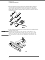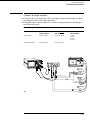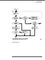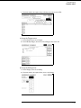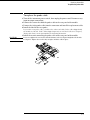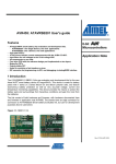
1
Service Guide Publication number 16555-97012 First edition, October 1996 For Safety information, Warranties, and Regulatory information, see the pages at the end of the book. Copyright Hewlett-Packard Company 1987–1996 All Rights Reserved. HP 16555A/D 110-MHz State/ 500-MHz Timing Logic Analyzers Notice Hewlett-Packard to Agilent Technologies Transition This manual may contain references to HP or Hewlett-Packard. Please note that HewlettPackard’s former test and measurement, semiconductor products and chemical analysis businesses are now part of Agilent Technologies. To reduce potential confusion, the only change to product numbers and names has been in the company name prefix: where a product name/number was HP XXXX the current name/number is now Agilent XXXX. For example, model number HP8648 is now model number Agilent 8648. Contacting Agilent Sales and Service Offices The sales and service contact information in this manual may be out of date. The latest service and contact information for your location can be found on the Web at: http://www.agilent.com/find/assist If you do not have access to the Internet, contact your field engineer or the nearest sales and service office listed below. In any correspondence or telephone conversation, refer to your instrument by its model number and full serial number. United States (tel) 1 800 452 4844 (fax) 1 800 829 4433 Latin America (tel) (305) 269 7500 (fax) (305) 269 7599 New Zealand (tel) 0 800 738 378 (fax) 64 4 495 8950 Canada (tel) +1 877 894 4414 (fax) +1 888 900 8921 Japan (tel) (81) 426 56 7832 (fax) (81) 426 56 7840 Asia Pacific (tel) (852) 3197 7777 (fax) (852) 2506 9284 Europe (tel) (31 20) 547 2323 (fax) (31 20) 547 2390 Australia (tel) 1 800 629 485 (fax) (61 3) 9210 5947 Printed in USA July 2004 HP 16555A/D 110-MHz State/500-MHz Timing Logic Analyzers The HP 16555A/D are 110-MHz State/500-MHz Timing Logic Analyzer modules for the HP 16500B/C Logic Analysis Systems. The HP 16555A/D offer high performance measurement capability. The HP 16555D has twice the memory depth of the HP 16555A. Features Some of the main features of the HP 16555A/D are as follows: • 64 data channels • 4 clock/data channels • 1016K memory depth per channel for the HP 16555A, 2032K memory depth per channel for the HP 16555D • 110 MHz maximum state acquisition speed • 500 MHz maximum timing acquisition speed • Expandable to 204 channels Service Strategy The service strategy for this instrument is the replacement of defective assemblies. This service guide contains information for finding a defective assembly by testing and servicing the HP 16555A/D state and timing analyzer modules. This module can be returned to Hewlett-Packard for all service work, including troubleshooting. Contact your nearest Hewlett-Packard Sales Office for more details. ii The HP 16555A/D Logic Analyzer iii In This Book This book is the service guide for the HP 16555A/D 110-MHz State/500-MHz Timing Logic Analyzer module. Place this service guide in the 3-ring binder supplied with your HP 16500B Logic Analysis System Service Manual or HP 16500C Logic Analysis System Service Manual. This service guide is divided into eight chapters. Chapter 1 contains information about the module and includes accessories for the module, specifications and characteristics of the module, and a list of the equipment required for servicing the module. Chapter 2 tells how to prepare the module for use. Chapter 3 gives instructions on how to test the performance of the module. Chapter 4 contains calibration instructions for the module. Chapter 5 contains self-tests and flowcharts for troubleshooting the module. Chapter 6 tells how to replace the module and assemblies of the module and how to return them to Hewlett-Packard. Chapter 7 lists replaceable parts, shows an exploded view, and gives ordering information. Chapter 8 explains how the analyzer works and what the self-tests are checking. iv Contents 1 General Information Accessories 1-2 Operating System 1-2 Specifications 1-3 Characteristics 1-4 Supplemental Characteristics 1-4 Recommended Test Equipment 1-7 2 Preparing For Use To inspect the module 2-2 To prepare the mainframe 2-3 To configure a one-card module 2-4 To configure a multicard module 2-5 To install the module 2-10 To turn on the system 2-11 To test the module 2-11 To install the ferrites 2-12 3 Testing Performance To perform the self-tests and make the test connectors 3-3 To test the threshold accuracy 3-9 To test the single-clock, single-edge, state acquisition 3-18 To test the multiple-clock, multiple-edge, state acquisition 3-30 To test the single-clock, multiple-edge, state acquisition 3-41 To test the time interval accuracy 3-51 To perform the multicard test 3-57 Performance Test Record 3-67 4 Calibrating 5 Troubleshooting To use the flowcharts 5-2 To run the self-tests 5-7 To run the Board Verification tests 5-8 To run the Acquisition IC Verification tests 5-10 To test the cables 5-13 To test the auxiliary power 5-17 6 Replacing Assemblies To remove the module 6-2 To replace the circuit board 6-3 To replace the module 6-3 To replace the probe cable 6-5 To replace the Reference Clock cable 6-6 To return assemblies 6-7 v Contents 7 Replaceable Parts Replaceable Parts Ordering 7-2 Replaceable Parts List 7-3 Exploded View 7-5 8 Theory of Operation Block-Level Theory 8-2 Self-Tests Description 8-6 vi 1 Accessories 1-2 Operating System 1-2 Specifications 1-3 Characteristics 1-4 Supplemental Characteristics 1-4 Recommended Test Equipment 1-7 General Information General Information This chapter lists the accessories, the specifications and characteristics, and the recommended test equipment. Accessories The following accessories are supplied with the HP 16555A/D Logic Analyzer. Accessories Supplied Probe Tip Assembly, Qty 4 Grabbers, Qty 4 packages Extra Probe Leads, Qty 1 package Extra Probe Grounds, Qty 4 packages Probe Cables, Qty 2 Probe Cable and Pod Labels, Qty 1 Double Probe Adapter, Qty 1 Ferrite Core Assembly, Qty 2 HP Part Number 01650-61608 5090-4356 5959-9333 5959-9334 16555-61606 01650-94310 16542-61607 16555-60001 Accessories Available The accessories available for the HP 16555A/D are listed in the Accessories for HP Logic Analyzers brochure. Operating System With HP 16500B Mainframe The HP 16555D Logic Analyzer requires operating system version v3.10 or higher. For the HP 16555A, the version of the operating system software depends on the programmable logic device that is the CPU interface. To verify the version of the programmable device, first locate the device, which is at the front of the HP 16555A board. If the programmable device has part number 16555-80001, then the device requires operating system version v2.xx, and the maximum state acquisition speed is 100 MHz. If the device has part number 16555-80002 or higher, then the device requires operating system v3.00 or higher, and the maximum state acquisition speed is 110 MHz for single-clock, single-edge clocking mode. You should always use the latest release, and must use version numbers that are compatible with your device. With HP 16500C Mainframe The HP 16555A/D Logic Analyzer requires operating system version v1.00 or higher. 1–2 General Information Specifications Specifications The specifications are the performance standards against which the product is tested. Minimum State Clock Pulse Width 1 3.5 ns Threshold Accuracy ± (100 mV + 3% of threshold setting) Clock Scheme: Single Clock, Single Edge: Setup/Hold Time: 1 Maximum State Speed Minimum Master-to-Master Clock Time 1 Single Clock, Multiple Edges: Setup/Hold Time: 1 0.0/3.5 ns through 3.5/0.0 ns, adjustable in 500-ps increments 110 MHz 2 9.09 ns 2 0.0/4.0 ns through 4.0/0.0 ns, adjustable in 500-ps increments 100 MHz Maximum State Speed Minimum Master-to-Master Clock Time 1 10.0 ns Multiple Clocks, Multiple Edges: Setup/Hold Time: 1 0.0/4.5 ns through 4.5/0.0 ns, adjustable in 500-ps increments Maximum State Speed 100 MHz 1 Minimum Master-to-Master Clock Time 10.0 ns 1 Specified for an input signal VH = −0.9 V, VL = −1.7 V, and threshold = −1.3 V. 2 An HP 16555A in an HP 16500B mainframe using operating system v2.xx has maximum state speed of 100 MHz and minimum Master-to-Master Clock Time of 10.0 ns for single-clock, single-edge clocking. 110-MHz single-clock state acquisition mode is available with HP 16500B mainframe operating system v3.00 or higher or HP 16500C mainframe operating system v1.00 or higher (refer to "Operating System"). The maximum state acquisition speed is 100 MHz for all other clocking modes. 1–3 General Information Characteristics Characteristics The characteristics are not specifications, but are included as additional information. Maximum State Clock Rate Maximum Conventional Timing Rate Channel Count per Card Channel Count per Three-Card Module Memory Depth (HP 16555A) Memory Depth (HP 16555D) Full Channel 110 MHz 250 MHz 68 204 1016K 2032K Half Channel * Not applicable 500 MHz 34 102 2088K 4177K * Half channel mode is only available for timing analysis. Supplemental Characteristics Probes Input Resistance Input Capacitance Minimum Voltage Swing 100 kΩ, ± 2% ~ 8 pF 500 mV, peak-to-peak Maximum Input Voltage ± 40 V, CAT I Threshold Range ± 6.0 V, adjustable in 50-mV increments Clock In/Out Clock Output 850 mV @100 MHz, terminated into 50 Ω. Clock Input 1.0 V @100 MHz, ± 20 Vdc offset (clock input port is terminated internally to 50 Ω). State Analysis State/Clock Qualifiers Time Tag Resolution* Maximum Time Count Between States 8 ns 34 seconds Maximum State Tag Count* 4.29 x 10⁹ Timing Analysis Sample Period Accuracy 0.01 % of sample period Channel-to-Channel Skew 2 ns, typical Time Interval Accuracy ± [sample period + channel-to-channel skew +(0.01%)(time reading)] 1–4 4 General Information Supplemental Characteristics Triggering Sequencer Speed State Sequence Levels Timing Sequence Levels Maximum Occurrence Counter Value Pattern Recognizers Maximum Pattern Width Range Recognizers Range Width Timers Timer Value Range Glitch/Edge Recognizers Maximum Glitch/Edge Width 125 MHz, maximum 12 10 1,048,575 10 68 channels in a one-card configuration. 204 channels in a three-card configuration. 2 32 bits each 2 400 ns to 500 seconds 2 (timing only) 68 channels in a one-card configuration. 204 channels in a three-card configuration. *Maximum state clock rate with time or state tags on is 110 MHz. When all pods are assigned to a state or timing machine, time or state tags halve the memory depth. Measurement and Display Functions Arming Each module can be armed by the RUN key, by the external PORT IN, or by another module via the Intermodule Bus (IMB). Displayed Waveforms 24 lines maximum, with scrolling across 96 waveforms. Measurement Functions Run/Stop Functions Run Starts acquisition of data in specified trace mode. Stop In single trace mode or the first run of a repetitive acquisition, STOP halts acquisition and displays the current acquisition data. For subsequent runs in repetitive mode, STOP halts acquisition of data and does not change the current display. Trace Mode Single mode acquires data once per trace specification. Repetitive mode repeats single mode acquisitions until stop is pressed or until the time interval between two specified patterns is less than or greater than a specified value, or within or not within a specified range. Indicators Activity Indicators Provided in the Configuration and Format menus for identifying high, low, or changing states on the inputs. Markers Two markers (X and 0) are shown as dashed lines on the display. Trigger Displayed as a vertical dashed line in the Timing Waveform display and as line 0 in the State Listing display. 1–5 General Information Supplemental Characteristics Data Entry/Display Labels Channels may be grouped together and given a 6-character name. Up to 126 labels in each analyzer may be assigned with up to 32 channels per label. Display Modes State listing, State Waveforms, Chart, Compare Listing, Compare Difference Listing, Timing Waveforms, and Timing Listings. State Listing, Timing Waveforms and Oscilloscope Waveforms can be time-correlated on the same displays. Timing Waveform Pattern readout of timing waveforms at X or 0 marker. Bases Binary, Octal, Decimal, Hexadecimal, ASCII (display only), Two’s Complement, and User-defined symbols. Symbols 1,000 maximum. Symbols can be downloaded over RS-232 or HP-IB. Marker Functions Time Interval The X and 0 markers measure the time interval between one point on a timing waveform and trigger, two points on the same timing waveform, two points on different waveforms, or two states (time tagging on). Delta States (state analyzer only) The X and 0 markers measure the number of tagged states between one state and trigger or between two states. Patterns The X and 0 markers can be used to locate the nth occurrence of a specified pattern from trigger, or from the beginning of data. The 0 marker can also find the nth occurrence of a pattern from the X marker. Statistics X and 0 marker statistics are calculated for repetitive acquisitions. Patterns must be specified for both markers and statistics are kept only when both patterns can be found in an acquisition. Statistics are minimum X to 0 time, maximum X to 0 time, average X to 0 time, and ratio of valid runs to total runs. Auxiliary Power Power Through Cables 1/3 amp at 5 V maximum per cable Operating Environment Temperature Humidity Altitude Vibration 1–6 Instrument, 0 °C to 55 °C (+32 °F to 131 °F). Probe lead sets and cables, 0 °C to 65 °C (+32 °F to 149 °F). Instrument, probe lead sets, and cables, up to 95% relative humidity at +40 °C (+122 °F). To 4600 m (15,000 ft). Operating: Random vibration 5 to 500 Hz, 10 minutes per axis, ≈ 0.3 g (rms). Non-operating: Random vibration 5 to 500 Hz, 10 minutes per axis, ≈ 2.41 g (rms); and swept sine resonant search, 5 to 500 Hz, 0.75 g (0-peak), 5 minute resonant dwell at 4 resonances per axis. General Information Recommended Test Equipment Recommended Test Equipment Equipment Required Equipment Critical Specifications Pulse Generator 110 MHz, 3.5 ns pulse width, < 600 ps rise time ≥ 6 GHz bandwidth, < 58 ps rise time Digitizing Oscilloscope Function Generator Digital Multimeter BNC-Banana Cable BNC Tee Cable SMA Coax Cable (Qty 3) BNC Coax Cable Adapter (Qty 4) Adapter Coupler 20:1 Probes (Qty 2) BNC Test Connector, 17x2 (Qty 1)** BNC Test Connector, 6x2 (Qty 4)** *A = Adjustment Accuracy ≤(5)(10−6) × frequency, DC offset voltage ±6.3 V 0.1 mV resolution, 0.005% accuracy BNC (m)(f)(f) BNC (m-m) 48 inch ≥ 18 GHz bandwidth BNC (m-m), >2 GHz bandwidth SMA(m)-BNC(f) SMA(f)-BNC(m) BNC (m-m) P = Performance Tests Recommended Model/Part HP 8131A Option 020 Use* HP 54750A mainframe with HP 54751A plugin module HP 3325B Option 002 P HP 3458A HP 11001-60001 HP 1250-0781 HP 10503A HP 8120-4948 HP 8120-1840 HP 1250-1200 HP 1250-2015 HP 1250-0216 HP 54006A P,T P P P P P P P P P P P P P,T T = Troubleshooting **Instructions for making these test connectors are in chapter 3, "Testing Performance." 1–7 1–8 2 To inspect the module 2-2 To prepare the mainframe 2-3 To configure a one-card module 2-4 To configure a multicard module 2-5 To install the module 2-10 To turn on the system 2-11 To test the module 2-11 To install the ferrites 2-12 Preparing for Use Preparing For Use This chapter gives you instructions for preparing the logic analyzer module for use. Power Requirements All power supplies required for operating the logic analyzer are supplied through the backplane connector in the mainframe. Operating Environment The operating environment is listed in chapter 1. Note the non-condensing humidity limitation. Condensation within the instrument can cause poor operation or malfunction. Provide protection against internal condensation. The logic analyzer module will operate at all specifications within the temperature and humidity range given in chapter 1. However, reliability is enhanced when operating the module within the following ranges: • Temperature: +20 °C to +35 °C (+68 °F to +95 °F) • Humidity: 20% to 80% non-condensing Storage Store or ship the logic analyzer in environments within the following limits: • Temperature: -40 °C to +75 °C • Humidity: Up to 90% at 65 °C • Altitude: Up to 15,300 meters (50,000 feet) Protect the module from temperature extremes which cause condensation on the instrument. To inspect the module 1 Inspect the shipping container for damage. If the shipping container or cushioning material is damaged, keep them until you have checked the contents of the shipment and checked the instrument mechanically and electrically. 2 Check the supplied accessories. Accessories supplied with the module are listed in chapter 1, "Accessories Supplied." 3 Inspect the product for physical damage. Check the module and the supplied accessories for obvious physical or mechanical defects. If you find any defects, contact your nearest Hewlett-Packard Sales Office. Arrangements for repair or replacement are made, at Hewlett-Packard’s option, without waiting for a claim settlement. 2–2 Preparing for Use To prepare the mainframe To prepare the mainframe CAUTION CAUTION Turn off the mainframe power before removing, replacing, or installing the module. Electrostatic discharge can damage electronic components. Use grounded wriststraps and mats when performing any service to this module. 1 Turn off the mainframe power switch, then unplug the power cord. Disconnect any input or output connections. 2 Plan your module configuration. If you are installing a one-card module, use any available slot in the mainframe. If you are installing a multicard module, use adjacent slots in the mainframe. 3 Loosen the thumb screws. Cards or filler panels below the slots intended for installation do not have to be removed. Starting from the top, loosen the thumb screws on filler panels and cards that need to be moved. 4 Starting from the top, pull the cards and filler panels that need to be moved halfway out. CAUTION All multicard modules will be cabled together. Pull these cards out together. 5 Remove the cards and filler panels. Remove the cards or filler panels that are in the slots intended for the module installation. Push all other cards into the card cage, but not completely in. This is to get them out of the way for installing the module. Some modules for the Logic Analysis System require calibration if you move them to a different slot. For calibration information, refer to the manuals for the individual modules. 2–3 Preparing for Use To configure a one-card module To configure a one-card module • When shipped separately, the module is configured as a one-card module. The cables should be connected as shown in the figure. • To configure a multicard module into one-card modules, remove the cables connecting the cards. Then connect the free end of the 2x10 cable to the connector labeled "Master" (J6) on each card (see figure below). CAUTION If you pull on the flexible ribbon part of the 2x10 cable, you might damage the cable assembly. Using your thumb and finger, grasp the ends of the cable connector. Apply pressure to the ends of the cable connector to disengage the metal locking tabs of the connector from the cable socket on the board. Then pull the connector from the cable socket. Save unused cables for future configurations. 2–4 Preparing for Use To configure a multicard module To configure a multicard module 1 Plan the configuration. Multicard modules can only be connected as shown in the illustration. Select the card that will be the master card, and set the remaining cards aside. Do not combine HP 16555A cards and HP 16555D cards together in a multicard module. A multicard module with both HP 16555A and HP 16555D cards will not operate. 2 Obtain two 2x25 cables from the accessory pouch that match the number of expanders being configured. The illustration shows the cables that are available and which cable is used in each expander configuration. 2–5 Preparing for Use To configure a multicard module 3 Look at the illustration in the previous step. The illustration shows which of the cable connectors is plugged into the master card. Plug one 2x25 cable into the master card J9. Observe which cable connector (as shown in the illustration) is plugged into J9. Follow the same procedure to connect the second 2x25 cable into the master card J10. 4 On the expander cards, disconnect the end of the 2x10 cable that is plugged into the connector labeled "Master." CAUTION If you pull on the flexible ribbon part of the 2x10 cable, you might damage the cable assembly. Using your thumb and finger, grasp the ends of the cable connector. Apply pressure to the ends of the cable connector to disengage the metal locking tabs of the connector from the cable socket on the board. Then pull the connector from the cable socket. 2–6 Preparing for Use To configure a multicard module 5 Place the master card above an expander card, if one is used. Plug the 2x25 cables into J9 and J10 of the expander card. 6 Feed the free end of the 2x10 cable of the expander cards through the access holes to the master card. Plug the 2x10 cable into J5 on the master card. 2–7 Preparing for Use To configure a multicard module 7 Place the remaining expander board on top of the master board. Feed the 2x25 cables that are plugged into the master card through the cable access holes of the expander card. Plug the 2x25 cables into J9 and J10 of the expander card. 8 Feed the free end of the 2x10 cables of the expander cards through the access holes to the master card. Plug the 2x10 cable into J7 on the master card. 2–8 Preparing for Use To configure a multicard module 9 The following illustration shows the proper connection of the 2x25 cables and the 2x10 cables for a three card module. A two card module is configured in the same manner, with the expansion card above the master card. Make sure ALL cables are firmly seated. 2–9 Preparing for Use To install the module To install the module 1 Slide the cards above the slots for the module about halfway out of the mainframe. 2 With the probe cables facing away from the instrument, slide the module approximately halfway into the mainframe. 3 Slide the complete module into the mainframe, but not completely in. Each card in the instrument is firmly seated and tightened one at a time in step 5. 4 Position all cards and filler panels so that the endplates overlap. 5 Seat the cards and tighten the thumbscrews. Starting with the bottom card, firmly seat the cards into the backplane connector of the mainframe. Keep applying pressure to the center of the card endplate while tightening the thumbscrews finger-tight. Repeat this for all cards and filler panels starting at the bottom and moving to the top. CAUTION Correct air circulation keeps the instrument from overheating. For correct air circulation, filler panels must be installed in all unused card slots. Keep any extra filler panels for future use. 2–10 Preparing for Use To turn on the system To turn on the system 1 Connect the power cable to the mainframe. 2 Turn on the instrument power switch. When you turn on the instrument power switch, the instrument performs powerup tests that check mainframe circuitry. After the powerup tests are complete, the screen will look similar to the sample screen below. The screen above is from an HP 16555A Logic Analyzer. The HP 16555D will appear as "2.0M SAMPLE 110/500MHz LA." To test the module The logic analyzer module does not require an operational accuracy calibration or adjustment. After installing the module, you can test and use the module. • If you require a test to verify the specifications, start at the beginning of chapter 3, "Testing Performance." • If you require a test to initially accept the operation, perform the self-tests in chapter 3. • If the module does not operate correctly, go to the beginning of chapter 5, "Troubleshooting." 2–11 Preparing for Use To install the ferrites To install the ferrites Ferrites are included in the HP 16555A/D accessory pouch for each logic analyzer cable (two pods). When properly installed, the ferrites reduce RFI emissions from the logic analyzer module. In order to ensure compliance of the HP 16555A/D analyzer module to the CISPR 11 Class A radio frequency interference (RFI) limits, you must install the ferrite to absorb radio frequency energy. Adding or removing the ferrite will not affect the normal operation of the analyzer. 1 Place the ferrite halves on the logic analyzer cable like a clamshell around the whole cable. The ferrite should be no more than 15 cm (about 6 in) from the rear panel of the logic analyzer. 2 Insert the clamps onto the ends of the ferrites. The locking tab should fit cleanly in the ferrite grooves. When properly installed, the ferrite should appear on the logic analyzer cable as shown below on the right. 2–12 3 To perform the self-tests and make the test connectors 3-3 To test the threshold accuracy 3-9 To test the single-clock, single-edge, state acquisition 3-18 To test the multiple-clock, multiple-edge, state acquisition 3-30 To test the single-clock, multiple-edge, state acquisition 3-41 To test the time interval accuracy 3-51 To perform the multicard test 3-57 Performance Test Record 3-67 Testing Performance Testing Performance This chapter tells you how to test the performance of the logic analyzer against the specifications listed in chapter 1. To ensure the logic analyzer is operating as specified, software tests (self-tests) and manual performance tests are done on the modules. The logic analyzer is considered performance-verified if all of the software tests and manual performance tests have passed. The procedures in this chapter indicate what constitutes a "Pass" status for each of the tests. Test Strategy For a complete test, start at the beginning with the software tests and continue through to the end of the chapter. For an individual test, follow the procedure in the test. One-card module To perform a complete test on a one-card module, start at the beginning of the chapter and follow each procedure. Multicard module To perform a complete test on a multicard module, perform the software tests with the cards connected. Then, remove the multicard module from the mainframe and configure each card as a one-card module. Install the one-card modules into the mainframe and perform the one-card manual performance tests on each card. When the tests are complete, remove the one-card modules, reconfigure them into a multicard module, reinstall the module into the mainframe, then perform the final multi-card test. For removal instructions, see chapter 6, "Replacing Assemblies." For installation and configuration instructions, see chapter 2, "Preparing for Use." Test Interval Test the performance of the module against specifications at two-year intervals. Test Record Description A performance test record for recording the results of each procedure is located at the end of this chapter. Use the performance test record to gauge the performance of the module over time. Test Equipment Each procedure lists the recommended test equipment. You can use equipment that satisfies the specifications given. However, the procedures are based on using the recommended model or part number. Instrument Warm-Up Before testing the performance of the module, warm-up the instrument and the test equipment for 30 minutes. 3–2 To perform the self-tests and make the test connectors The self-tests verify the correct operation of the logic analyzer module. Self-tests can be performed all at once or one at a time. While testing the performance of the module, run the self-test all at once. The test connectors connect the analyzer to the test equipment. Perform the self-tests 1 Disconnect all inputs. 2 In the System Configuration menu, touch Configuration. In the pop-up, touch Test. 3 Touch the box labeled Touch Box to Load Test System. 4 On the test system screen, touch Test System. Select the module to be tested. For an HP 16555A, select 1M Sample LA as the module to be tested. For an HP 16555D, select 2M Sample LA. 3–3 Testing Performance To perform the self-tests and make the test connectors 5 In the Performance Verification menu, touch the field labeled Board Verification. 6 In the Board Verification menu, touch All Tests. You can run all tests at one time by touching All Tests. To see more details about each test when troubleshooting failures, you can run each test individually. This example shows how to run all tests at once. 7 When the tests finish, the status will show Passed or Failed. Record the results of the Board Verification tests in the performance test record at the end of this chapter. 3–4 Testing Performance To perform the self-tests and make the test connectors 8 Touch Exit to leave the Board Verification menu. In the Performance Verification menu, touch the field labeled Acquisition IC Verification. 9 In the Acquisition IC Verification menu, touch All Tests. You can run all tests at one time by touching All Tests. To see more details about each test when troubleshooting failures, you can run each test individually. This example shows how to run all tests at once. 10 When the tests finish, the status will show Passed or Failed. Record the results of the Acquisition IC Verification tests in the performance test record at the end of this chapter. 3–5 Testing Performance To perform the self-tests and make the test connectors 11 Touch 1M Sample LA (HP 16555A) or 2M Sample LA (HP 16555D). If more logic analyzer cards are to be tested, select the next card, then repeat the test. When all cards are tested, touch 1M Sample LA (or 2M Sample LA), then select Test System. 12 Touch Configuration, then select Test. In the Test menu, touch the box labeled Touch box to Exit Test System. 3–6 Testing Performance To perform the self-tests and make the test connectors Make the test connectors Materials Required Description Recommended Part Qty BNC (f) Connector HP 1250-1032 5 100 Ω 1% resistor HP 0698-7212 8 Berg Strip, 17-by-2 1 Berg Strip, 6-by-2 4 20:1 Probe HP 54006A 2 Jumper wire 1 Build four test connectors using BNC connectors and 6-by-2 sections of Berg strip. a Solder a jumper wire to all pins on one side of the Berg strip. b Solder a jumper wire to all pins on the other side of the Berg strip. c Solder two resistors to the Berg strip, one at each end between the end pins. d Solder the center of the BNC connector to the center pin of one row on the Berg strip. e Solder the ground tab of the BNC connector to the center pin of the other row on the Berg strip. f On two of the test connectors, solder a 20:1 probe. The probe ground goes to the same row of pins on the test connector as the BNC ground tab. 3–7 Testing Performance To perform the self-tests and make the test connectors 2 Build one test connector using a BNC connector and a 17-by-2 section of Berg strip. a Solder a jumper wire to all pins on one side of the Berg strip. b Solder a jumper wire to all pins on the other side of the Berg strip. c Solder the center of the BNC connector to the center pin of one row on the Berg strip. d Solder the ground tab of the BNC connector to the center pin of the other row on the Berg strip. 3–8 To test the threshold accuracy Testing the threshold accuracy verifies the performance of the following specification: • Clock and data channel threshold accuracy. Multicard modules must be reconfigured as one-card modules for this test. These instructions include detailed steps for testing the threshold settings of pod 1. After testing pod 1, connect and test the rest of the pods one at a time. To test the next pod, follow the detailed steps for pod 1, substituting the next pod for pod 1 in the instructions. Equipment Required Equipment Digital Multimeter Function Generator BNC-Banana Cable BNC Tee BNC Cable BNC Test Connector, 17x2 Critical Specifications 0.1 mV resolution, 0.005% accuracy DC offset voltage ±6.3 V Recommended Model/Part HP 3458A HP 3325B Option 002 HP 11001-60001 HP 1250-0781 HP 8120-1840 Set up the equipment 1 Turn on the equipment required and the logic analyzer. Let them warm up for 30 minutes before beginning the test. 2 Set up the function generator. a Set up the function generator to provide a DC offset voltage at the Main Signal output. b Disable any AC voltage to the function generator output, and enable the high voltage output. c Monitor the function generator DC output voltage with the multimeter. 3–9 Testing Performance To test the threshold accuracy Set up the logic analyzer 1 In the System Configuration menu, touch System, then select 1M Sample LA (HP 16555A) or 2M Sample LA (HP 16555D). 2 In the Configuration menu, unassign Pod 3 and Pod 4. To unassign the pods, touch the Pod 3, Pod 4 field, then select Unassigned. Pod 3, Pod 4 field Connect the logic analyzer 1 Using the 17-by-2 test connector, BNC cable, and probe tip assembly, connect the data and clock channels of Pod 1 to one side of the BNC Tee. 2 Using a BNC-banana cable, connect the voltmeter to the other side of the BNC Tee. 3 Connect the BNC Tee to the Main Signal output of the function generator. 3–10 Testing Performance To test the threshold accuracy Test the TTL threshold 1 In the Configuration menu, touch Configuration, then touch Format. In the Format menu, touch the field to the right of Pod 1, then select TTL. 2 On the function generator front panel, enter 1.647 V ±1 mV DC offset. Use the multimeter to verify the voltage. The activity indicators for Pod 1 should show all data channels and the J-clock channel at a logic high. 3 Using the Modify down arrow on the function generator, decrease offset voltage in 1-mV increments until all activity indicators for Pod 1 show the channels at a logic low. Record the function generator voltage in the performance test record. 3–11 Testing Performance To test the threshold accuracy 4 Using the Modify up arrow on the function generator, increase offset voltage in 1-mV increments until all activity indicators for Pod 1 show the channels at a logic high. Record the function generator voltage in the performance test record. 3–12 Testing Performance To test the threshold accuracy Test the ECL threshold 1 In the Format menu, touch the field to the right of Pod 1, then select ECL. 2 On the function generator front panel, enter −1.159 V ±1 mV DC offset. Use the multimeter to verify the voltage. The activity indicators for Pod 1 should show all data channels and the J-clock channel at a logic high. 3 Using the Modify down arrow on the function generator, decrease offset voltage in 1-mV increments until all activity indicators for Pod 1 show the channels are at a logic low. Record the function generator voltage in the performance test record. 4 Using the Modify up arrow on the function generator, increase offset voltage in 1-mV increments until all activity indicators for Pod 1 show the channels are at a logic high. Record the function generator voltage in the performance test record. 3–13 Testing Performance To test the threshold accuracy Test the − User threshold 1 In the Format menu, touch the field to the right of Pod 1, then select User. In the pop-up menu, enter −6.00 V, then touch Done. 2 On the function generator front panel, enter −5.718 V ±1 mV DC offset. Use the multimeter to verify the voltage. The activity indicators for Pod 1 should show all data channels and the J-clock channel at a logic high. 3 Using the Modify down arrow on the function generator, decrease offset voltage in 1-mV increments until all activity indicators for Pod 1 show the channels at a logic low. Record the function generator voltage in the performance test record. 4 Using the Modify up arrow on the function generator, increase offset voltage in 1-mV increments until all activity indicators show the channels at a logic high. Record the function generator voltage in the performance test record. 3–14 Testing Performance To test the threshold accuracy Test the + User threshold 1 In the Format menu, touch the field to the right of Pod 1, then select User. In the pop-up menu, enter +6.00 V, then touch Done. 2 On the function generator front panel, enter +6.282 V ±1 mV DC offset. Use the multimeter to verify the voltage. The activity indicators for Pod 1 should show all data channels and the J-clock channel at a logic high. 3 Using the Modify down arrow on the function generator, decrease offset voltage in 1-mV increments until all activity indicators for Pod 1 show the channels at a logic low. Record the function generator voltage in the performance test record. 4 Using the Modify up arrow on the function generator, increase offset voltage in 1-mV increments until all activity indicators for Pod 1 show the channels at a logic high. Record the function generator voltage in the performance test record. 3–15 Testing Performance To test the threshold accuracy Test the 0 V User threshold 1 In the Format menu, touch the field to the right of Pod 1, then select User. In the pop-up menu, enter 0.00 V, then touch Done. 2 On the function generator front panel, enter +0.102 V ±1 mV DC offset. Use the multimeter to verify the voltage. The activity indicators for Pod 1 should show all data channels and the J-clock channel at a logic high. 3 Using the Modify down arrow on the function generator, decrease offset voltage in 1-mV increments until all activity indicators for Pod 1 show the channels at a logic low. Record the function generator voltage in the performance test record. 4 Using the Modify up arrow on the function generator, increase offset voltage in 1-mV increments until all activity indicators for Pod 1 show the channels at a logic high. Record the function generator voltage in the performance test record. 3–16 Testing Performance To test the threshold accuracy Test the next pod Using the 17-by-2 test connector and probe tip assembly, connect the data and clock channels of the next pod to the output of the function generator. • If you just finished testing Pod 1, connect the data and clock channels of Pod 2. Start with "Test the TTL threshold" on page 3–11, substituting Pod 2 for Pod 1. • If you just finished testing Pod 2, connect the data and clock channels of pod 3. In the logic analyzer Configuration menu, unassign Pods 1 and 2, assign Pods 3 and 4 to Machine 1. Start with "Test the TTL threshold" on page 3–11, substituting Pod 3 for Pod 1. • If you just finished testing Pod 3, connect the data and clock channels of Pod 4. Start with "Test the TTL threshold" on page 3–11, substituting Pod 4 for Pod 1. • If you just finished testing Pod 4, you have completed the threshold accuracy test. 3–17 To test the single-clock, single-edge, state acquisition Testing the single-clock, single-edge, state acquisition verifies the performance of the following specifications: • • • • Minimum master to master clock time. Maximum state acquisition speed. Setup/Hold time. Minimum clock pulse width. Multicard modules must be reconfigured as one-card modules for this test. This test checks a combination of data channels using a single-edge clock at three selected setup/hold times. Equipment Required Equipment Critical Specifications Pulse Generator 110 MHz 3.5 ns pulse width, <600 ps rise time Digitizing Oscilloscope ≥ 6 GHz bandwidth, <58 ps rise time Adapter SMA(m)-BNC(f) SMA Coax Cable (Qty 3) Coupler (Qty 3) BNC(m-m) BNC Test Connector, 6x2 (Qty 3) Recommended Model/Part HP 8131A option 020 HP 54750A w/ HP 54751A HP 1250-1200 HP 8120-4948 HP 1250-0216 Set up the equipment 1 Turn on the equipment required and the logic analyzer. Let them warm up for 30 minutes before beginning the test if you have not already done so. 2 Set up the pulse generator according to the following table. Pulse Generator Setup Channel 1 Channel 2 Period Delay: 0 ps Doub: 9.05 ns * 18.1 ns * Width: 3.5 ns Width: 3.5 ns High: -0.9 V High: -0.9 V Low: -1.7 V Low: -1.7 V COMP: Disabled (LED off) COMP: Disabled (LED off) * If running HP 16500B mainframe software version v2.xx on an HP 16555A, set Channel 2 Doub: 10 ns, and Period to 20 ns. 110-MHz single-clock state acquisition mode is available with HP 16500B mainframe operating system v3.00 or higher or HP 16500C mainframe operating system v1.00 or higher. For information on software version, refer to "Operating System" in chapter 1. 3–18 Testing Performance To test the single-clock, single-edge, state acquisition 3 Set up the oscilloscope. a Select Setup, then select Default Setup. b Configure the oscilloscope according to the following table. Oscilloscope Setup Acquisition Display Trigger [Shift] ∆ Time Averaging: On # of averages: 16 Graticule Graphs: 2 Level: -250 mV Stop src: channel 2 [Enter] Channel 1 Channel 2 Define meas Alternate Scale Attenuation: 20.00:1 Scale: 200 mV/div Offset: −1.300 V Alternate Scale Attenuation: 20.00:1 Scale: 200 mV/div Offset: -1.300 V Thresholds: user-defined Units: Volts Upper: -980 mV Middle: -1.30 V Lower: -1.62 V Set up the logic analyzer 1 Set up the Configuration menu. a In the System Configuration menu, touch System, then select 1M Sample LA (2M Sample LA for HP 16555D). b In the Configuration menu, assign all pods to Machine 1. To assign the pods, touch the pod fields, then select Machine 1. c In the Analyzer 1 box, touch the Type field, then select State. 3–19 Testing Performance To test the single-clock, single-edge, state acquisition 2 Set up the Format menu. a Touch Configuration, then select Format. b Touch the field to the right of each Pod field, then select ECL. The screen does not show all Pod fields at one time. To access more Pod fields, turn the knob. c Touch the field showing the channel assignments for one of the pods being tested. In the pop-up menu, touch Clear until all "." appear. Using the knob, move the cursor to the data channels to be tested (channel 11 and channel 3 of each pod). Touch the asterisk field to put asterisks in the channel positions, activating the channels, then touch Done. Follow this step for the remaining three pods. d Touch the State Acquisition Mode field, then select 110MHz/1M State (110MHz/2M State for HP 16555D).* *110-MHz single-clock state acquisition mode is not available with HP 16555A operating system v2.xx . Refer to page 1-2 3 Set up the Trigger menu. a Touch Format, then select Trigger. In the Trigger menu, touch Modify Trigger, then select Clear Trigger, then select All. b Touch the Count Off field. In the Count menu, touch Off. In the pop-up, select Time, then touch Done to exit. c Touch the Acquisition Control field. In the Acquisition Control menu, touch Trigger Position then touch Start. Touch Memory Length, and at the numeric keypad, enter "4096" and Touch Done. Touch Done to exit the menu. d Touch the field labeled "1" under the State Sequence Levels. Touch the field labeled "anystate," then select "no state." Touch Done. e Touch the pattern recognizer "a." In the pop-up menu, type "AA," then touch Done. 3–20 Testing Performance To test the single-clock, single-edge, state acquisition 4 Set up the Listing menu. a Touch Trigger, then select Listing. b Touch the Markers field, then select Pattern. c Touch Specify Patterns. Select the X Marker > field. At the numeric keypad, enter "AA." Select the O Marker > field. At the numeric keypad, enter "55." Touch Done. d Touch the Find X-pattern occurrences field. At the numeric keypad, enter "2047." Touch Done. e Touch the Find X-pattern field. The field should toggle to Find O-pattern. f Touch the Find O-pattern occurrences field. At the numeric keypad, enter "2048." Touch Done. 3–21 Testing Performance To test the single-clock, single-edge, state acquisition Connect the logic analyzer 1 Using the 6-by-2 test connectors, connect the logic analyzer clock and data channels listed in the table below to the pulse generator. 2 Using SMA cables, connect channel 1, channel 2, and trigger from the oscilloscope to the pulse generator. Connect the Logic Analyzer to the Pulse Generator Connect to HP 8131A Channel 1 Output Connect to HP 8131A Channel 1 Output Connect to HP 8131A Channel 2 Output Pod 1, channel 3 Pod 2, channel 3 Pod 3, channel 3 Pod 4, channel 3 Pod 1, channel 11 Pod 2, channel 11 Pod 3, channel 11 Pod 4, channel 11 J-clock K-clock L-clock M-clock 3–22 Testing Performance To test the single-clock, single-edge, state acquisition Verify the test signal 1 Check the clock pulse width. Using the oscilloscope, verify that the clock pulse width is 3.480 ns, +20 ps or -80 ps. a Enable the pulse generator channel 1 and channel 2 outputs (LED off). b In the oscilloscope Timebase menu, select Scale: 1.000 ns/div. c In the oscilloscope Timebase menu, select Position. Using the oscilloscope knob, position the clock waveform so that the waveform is centered on the screen. d On the oscilloscope, select [Shift] + width: channel 2, then select [Enter] to display the clock signal pulse width (+ width(2)). e If the pulse width is outside the limits, adjust the pulse generator channel 2 width until the pulse width is within limits. 3–23 Testing Performance To test the single-clock, single-edge, state acquisition 2 Check the clock period. Using the oscilloscope, verify that the master-to-master clock time is 9.05 ns. * a In the oscilloscope Timebase menu, select Scale: 2.000 ns/div. b In the oscilloscope Timebase menu, select Position. Using the oscilloscope knob, position the clock waveform so that a rising edge appears at the left of the display. c On the oscilloscope, select [Shift] Period: channel 2, then select [Enter] to display the clock period (Period(2)). If the period is not less than 9.05 ns, go to step d. If the period is less than 9.05 ns, go to step 3. d In the oscilloscope Timebase menu, increase Position 9.000 ns. If the period is not less than 9.05 ns, decrease the pulse generator Chan 2 Doub in 10 ps increments until one of the two periods measured is less than 9.05 ns. *If running operating system version HP 16555A operating system v2.xx, measure a master-to-master clock time of 10 ns. 3 Check the data pulse width. Using the oscilloscope, verify that the data pulse width is 3.480 ns, +20 ps or - 80 ps. a In the oscilloscope Timebase menu, select Scale: 1.000 ns/div. b In the oscilloscope Timebase menu, select Position. Using the oscilloscope knob, position the data waveform so that the waveform is centered on the screen. c On the oscilloscope, select [Shift] + width: channel 1, then select [Enter] to display the data signal pulse width (+ width(1)). d If the pulse width is outside the limits, adjust the pulse generator channel 1 width until the pulse width is within limits. 3–24 Testing Performance To test the single-clock, single-edge, state acquisition Check the setup/hold combination 1 Select the logic analyzer setup/hold time. a Touch Listing, then touch Format. b In the logic analyzer Format menu, touch Master Clock. c Touch the Setup/Hold field and select the setup/hold combination to be tested for all pods. The first time through this test, select the top combination in the following table. Setup/Hold Combinations 3.5/0.0 ns 0.0/3.5 ns 1.5/2.0 ns d Touch Done to exit the setup/hold combinations. 2 Disable the pulse generator channel 2 COMP (LED off). 3–25 Testing Performance To test the single-clock, single-edge, state acquisition 3 Using the Delay mode of the pulse generator channel 1, position the pulses according to the setup/hold combination selected, +0.0 ps or -100 ps. a On the Oscilloscope, select [Define meas] Define ∆Time - Stop edge: rising. b In the oscilloscope timebase menu, select Position. Using the oscilloscope knob, position the rising edge of the clock waveform so that it is centered on the display. c On the oscilloscope, select [Shift] ∆ Time, then select [Enter] to display the setup time (∆Time(1)-(2)). d Adjust the pulse generator channel 1 Delay until the pulses are aligned according the the setup time of the setup/hold combination selected, +0.0 ps or -100 ps. 4 Select the clock to be tested. a In the Master Clock menu, touch the clock field to be tested and then select the clock edge as indicated in the table. The first time through this test, select the first clock and edge. Clocks J↑ K↑ L↑ M↑ b Touch Done to exit the Master Clock menu. Note: The Master Clock menu shown is for an HP 16555A 1M Sample analyzer running in 110-MHz mode. If HP 16555A operating system version v2.xx is being used, the Master Clock menu will look similar to that shown on page 3-38. 3–26 Testing Performance To test the single-clock, single-edge, state acquisition 5 In the logic analyzer Format menu, touch Run. The display should show an alternating pattern of "AA" and "55." If the "Search Failed" yellow bar message does not appear, the test passes. Record the Pass or Fail in the performance test record. 6 Test the next clock. a Touch Listing, then touch Format. b In the logic analyzer Format menu, touch Master Clock. c Turn off the clock just tested. d Repeat steps 4, 5, and 6 for the next clock edge listed in the table in step 4, until all listed clock edges have been tested. 7 Enable the pulse generator channel 2 COMP (LED on). 8 Using the Delay mode of the pulse generator channel 1, position the pulses according to the setup/hold combination selected, +0.0 ps or -100 ps. a On the Oscilloscope, select [Define meas] Define ∆Time - Stop edge: falling. b On the oscilloscope, select [Shift] - width: channel 2, then select [Enter] to verify the clock signal pulse width (- width(2)). If the pulse width is outside the limits, adjust the pulse generator channel 2 width until the clock pulse width is 3.480 ns, +20 ps or -80 ps. c On the oscilloscope, select [Shift] ∆Time. Select Start src: channel 1, then select [Enter] to display the setup time (∆Time(1)-(2)). d Adjust the pulse generator channel 1 Delay until the pulses are aligned according the the setup time of the setup/hold combination selected, +0.0 ps or -100 ps. 3–27 Testing Performance To test the single-clock, single-edge, state acquisition 9 Select the clock to be tested. a In the Master Clock menu, touch the clock field to be tested and then select the clock edge as indicated in the table. The first time through this test, select the top clock and edge. Clocks J↓ K↓ L↓ M↓ b Touch Done to exit the Master Clock menu. 10 In the logic analyzer Format menu, touch Run. The display should show an alternating pattern of AA and 55. If the "Search Failed" yellow bar message does not appear, the test passes. Record the Pass or Fail results in the performance test record. 3–28 Testing Performance To test the single-clock, single-edge, state acquisition 11 Test the next clock. a In the logic analyzer Format menu, touch Master Clock. b Turn off the clock just tested. c Repeat steps 9, 10, and 11 for the next clock edge listed in the table in step 9, until all listed clock edges have been tested. 12 Test the next setup/hold combination. a In the logic analyzer Format menu, touch Master Clock. b Turn off the clock just tested. c Repeat steps 1 through 12 for the next setup/hold combination listed in step 1 on page 3–25, until all listed setup/hold combinations have been tested. When aligning the data and clock waveforms using the oscilloscope, align the waveforms according to the setup time of the setup/hold combination being tested, +0.0 ps or −100 ps. 3–29 To test the multiple-clock, multiple-edge, state acquisition Testing the multiple-clock, multiple-edge, state acquisition verifies the performance of the following specifications: • • • • Minimum master to master clock time. Maximum state acquisition speed. Setup/Hold time. Minimum clock pulse width. Multicard modules must be reconfigured as one-card modules for this test. This test checks a combination of data channels using multiple clocks at three selected setup/hold times. Equipment Required Equipment Critical Specifications Pulse Generator 100 MHz 3.5 ns pulse width, <600 ps rise time Digitizing Oscilloscope ≥ 6 GHz bandwidth, <58 ps rise time Adapter SMA(m)-BNC(f) SMA Coax Cable (Qty 3) Coupler (Qty 3) BNC(m-m) BNC Test Connector, 6x2 (Qty 3) Recommended Model/Part HP 8131A option 020 HP 54750A w/ HP 54751A HP 1250-1200 HP 8120-4948 HP 1250-0216 Set up the equipment 1 Turn on the equipment required and the logic analyzer. Let them warm up for 30 minutes before beginning the test if you have not already done so. 2 Set up the pulse generator according to the following table. Pulse Generator Setup Channel 1 Channel 2 Period Delay: 0 ps Doub: 10.0 ns 20.0 ns Width: 4.5 ns Width: 3.5 ns High: −0.9 V High: −0.9 V Low: −1.7 V Low: −1.7 V COMP: Disabled (LED off) COMP: Disabled (LED off) 3–30 Testing Performance To test the multiple-clock, multiple-edge, state acquisition 3 Set up the oscilloscope. If the oscilloscope was not configured for the previous test, then do the following steps. a Select Setup, then select Default Setup. b Configure the oscilloscope according to the following table. Oscilloscope Setup Acquisition Display Trigger [Shift] ∆ Time Averaging: On # of averages: 16 Graticule Graphs: 2 Level: -250 mV Stop src: channel 2 [Enter] Channel 1 Channel 2 Define meas Alternate Scale Attenuation: 20.00:1 Scale: 200 mV/div Offset: −1.300 V Alternate Scale Attenuation: 20.00:1 Scale: 200 mV/div Offset: -1.300 V Thresholds: user-defined Units: Volts Upper: -980 mV Middle: -1.30 V Lower: -1.62 V Set up the logic analyzer 1 Set up the Configuration menu. a In the System Configuration menu, touch System, then select 1M Sample LA (2M Sample LA for HP 16555D). b In the Configuration menu, assign all pods to Machine 1. To assign all pods, touch the pod fields, then select Machine 1. c In the Analyzer 1 box, touch the Type field, then select State. 3–31 Testing Performance To test the multiple-clock, multiple-edge, state acquisition 2 Set up the Format menu. a Touch Configuration, then select Format. b Touch the field to the right of each Pod field, then select ECL. The screen does not show all Pod fields at one time. To access more Pod fields, turn the knob. c Touch the field showing the channel assignments for one of the pods being tested. In the pop-up menu, touch Clear until all "." appear. Using the knob, move the cursor to the data channels to be tested (channel 11 and channel 3 of each pod). Touch the asterisk field to put asterisks in the channel positions, activating the channels, then touch Done. Follow this step for the remaining three pods. 3 Set up the Trigger menu. a Touch Format, then select Trigger. In the Trigger menu, touch Modify Trigger, then select Clear Trigger, then select All. b Touch the Count Off field. In the Count menu, touch Off. In the pop-up, select Time, then touch Done to exit. c Touch the Acquisition Control field. In the Acquisition Control menu, touch Trigger Position then touch Start. Touch Memory Length, and at the numeric keypad, enter "4096" and Touch Done. Touch Done to exit the menu. d Touch the field labeled "1" under the State Sequence Levels. Touch the field labeled "anystate," then select "no state." Touch Done. e Touch the pattern recognizer "a." In the pop-up menu, type "AA," then touch Done. 3–32 Testing Performance To test the multiple-clock, multiple-edge, state acquisition 4 Set up the Listing menu. a Touch Trigger, then select Listing. b Touch the Markers field, then select Pattern. c Touch Specify Patterns. Select the X Marker > field. At the numeric keypad, enter "AA." Select the O Marker > field. At the numeric keypad, enter "55." Touch Done. d Touch the Find X-pattern occurrences field. At the numeric keypad, enter "2047." Touch Done. e Touch the Find X-pattern field. The field should toggle to Find O-pattern. f Touch the Find O-pattern occurrences field. At the numeric keypad, enter "2048." Touch Done. 3–33 Testing Performance To test the multiple-clock, multiple-edge, state acquisition Connect the logic analyzer 1 Using the 6-by-2 test connectors, connect the logic analyzer clock and data channels listed in the table below to the pulse generator. 2 Using SMA cables, connect channel 1, channel 2, and trigger of the oscilloscope to the pulse generator. Connect the Logic Analyzer to the Pulse Generator Connect to HP 8131A Channel 1 Output Connect to HP 8131A Channel 1 Output Connect to HP 8131A Channel 2 Output Pod 1, channel 3 Pod 2, channel 3 Pod 3, channel 3 Pod 4, channel 3 Pod 1, channel 11 Pod 2, channel 11 Pod 3, channel 11 Pod 4, channel 11 J-clock K-clock L-clock M-clock 3–34 Testing Performance To test the multiple-clock, multiple-edge, state acquisition Verify the test signal 1 Check the clock pulse width. Using the oscilloscope, verify that the clock pulse width is 3.480 ns, +20 ps or -80 ps. a Enable the pulse generator channel 1 and channel 2 outputs (LED off). b In the oscilloscope Timebase menu, select Scale: 1.000 ns/div. c In the oscilloscope Timebase menu, select Position. Using the oscilloscope knob, position the clock waveform so that the waveform is centered on the screen. d On the oscilloscope, select [Shift] + width: channel 2, then select [Enter] to display the clock signal pulse width (+ width (2)). e If the pulse width is outside the limits, adjust the pulse generator channel 2 width until the pulse width is within limits. 3–35 Testing Performance To test the multiple-clock, multiple-edge, state acquisition 2 Check the clock period. Using the oscilloscope, verify that the master-to-master clock time is 10.000 ns. a In the oscilloscope Timebase menu, select Scale: 2.000 ns/div b In the oscilloscope Timebase menu, select Position. Using the oscilloscope knob, position the clock waveform so that a rising edge appears at the left of the display c On the oscilloscope, select [Shift] Period: channel 2, then select [Enter] to display the clock period (Period(2)). If the period is not less than 10.000 ns, go to step d. If the period is less than 10.000 ns, go to step 3. d In the oscilloscope Timebase menu, increase Position 10.000 ns. If the period is not less than 10.000 ns, decrease the pulse generator Chan 2 Doub in 10 ps increments until one of the two periods measured is less than 10.000 ns. 3 Check the data pulse width. Using the oscilloscope, verify that the data pulse width is 4.480 ns, +20 ps or - 80 ps. a In the oscilloscope Timebase menu, select Scale: 1.000 ns/div. b In the oscilloscope Timebase menu, select Position. Using the oscilloscope knob, position the data waveform so that the waveform is centered on the screen. c On the oscilloscope, select [Shift] + width: channel 1, then select [Enter] to display the data signal pulse width (+ width (1)). d If the pulse width is outside the limits, adjust the pulse generator channel 1 width until the pulse width is within limits. 3–36 Testing Performance To test the multiple-clock, multiple-edge, state acquisition Check the setup/hold with single clock edges, multiple clocks 1 Select the logic analyzer setup/hold time. a Touch Listing, then touch Format. In the logic analyzer Format menu, touch Master Clock. b Select and activate any two clock edges. c Touch the Setup/Hold field and select the setup/hold to be tested for all pods. The first time through this test, select the top combination in the following table. Setup/Hold Combinations 4.5/0.0 ns 0.0/4.5 ns 2.0/2.5 ns d Touch Done to exit the setup/hold combinations. 2 Disable the pulse generator channel 2 COMP (LED off). 3–37 Testing Performance To test the multiple-clock, multiple-edge, state acquisition 3 Using the Delay mode of the pulse generator channel 1, position the pulses according to the setup/hold combination selected, +0.0 ps or -100 ps. a On the Oscilloscope, select [Define meas] Define ∆ Time - Stop edge: rising. b In the oscilloscope timebase menu, select Position. Using the oscilloscope knob, position the rising edge of the clock waveform so that it is centered on the display. c On the oscilloscope, select [Shift] ∆ Time, then select [Enter] to display the setup time (∆ Time(1)-(2)). d Adjust the pulse generator channel 1 Delay until the pulses are aligned according the the setup time of the setup/hold combination selected, +0.0 ps or -100 ps. 4 Select the clocks to be tested. a Touch the clock field to be tested, and then select the following combination of clock edges: J↑ + K↑ + L↑ + M↑. b Touch Done to exit the Master Clock menu. 3–38 Testing Performance To test the multiple-clock, multiple-edge, state acquisition 5 In the logic analyzer Format menu, touch Run. The display should show an alternating pattern of AA and 55. If the "Search Failed" yellow bar message does not appear, the test passes. Record the Pass or Fail results in the performance test record. 6 Enable the pulse generator channel 2 COMP (LED on). 7 Using the Delay mode of the pulse generator channel 1, position the pulses according to the setup/hold combination selected, +0.0 ps or -100 ps. a On the Oscilloscope, select [Define meas] Define ∆Time - Stop edge: falling. b On the oscilloscope, select [Shift] - width: channel 2, then select [Enter] to verify the clock signal pulse width (- width (2)). If the pulse width is outside the limits, adjust the pulse generator channel 2 width until the clock pulse width is 3.480 ns, +20 ps or -80 ps. c On the oscilloscope, select [Shift] ∆Time. Select Start src: channel 1, then select [Enter] to display the setup time (∆Time(1)-(2)). d Adjust the pulse generator channel 1 Delay until the pulses are aligned according the the setup time of the setup/hold combination selected, +0.0 ps or -100 ps. 3–39 Testing Performance To test the multiple-clock, multiple-edge, state acquisition 8 Select the clocks to be tested. a Touch the clock field to be tested and then select the following combination of clock edges: J↓ + K↓ + L↓ + M↓. b Touch Done to exit the Master Clock menu. 9 In the logic analyzer Format menu, touch Run. The display should show an alternating pattern of AA and 55. If the "Search Failed" yellow bar message does not appear, the test passes. Record the Pass or Fail results in the performance test record. 10 Test the next setup/hold combination. a In the logic analyzer Format menu, touch Master Clock. b Turn off the clocks just tested. c Repeat steps 1 through 10 for the next setup/hold combination listed in step 1 on page 3-37, until all listed setup/hold combinations have been tested. When aligning the data and clock waveforms using the oscilloscope, align the waveforms according to the setup time of the setup/hold combination being tested, +0.0 ps or −100 ps. 3–40 To test the single-clock, multiple-edge, state acquisition Testing the single-clock, multiple-edge, state acquisition verifies the performance of the following specifications: • • • • Minimum master to master clock time. Maximum state acquisition speed. Setup/Hold time. Minimum clock pulse width. Multicard modules must be reconfigured as one-card modules for this test. This test checks a combination of data channels using a multiple-edge single clock at three selected setup/hold times. Equipment Required Equipment Critical Specifications Pulse Generator Digitizing Oscilloscope Adapter SMA Coax Cable (Qty 3) Coupler (Qty 3) BNC Test Connector, 6x2 (Qty 3) 100 MHz 3.5 ns pulse width, <600 ps rise time ≥ 6 GHz bandwidth, <58 ps rise time SMA(m)-BNC(f) BNC(m-m) Recommended Model/Part HP 8131A option 020 HP 54750A w/ HP 54751A HP 1250-1200 HP 8120-4948 HP 1250-0216 Set up the equipment 1 Turn on the equipment required and the logic analyzer. Let them warm up for 30 minutes before beginning the test if you have not already done so. 2 Set up the pulse generator according to the following table. Pulse Generator Setup Channel 1 Channel 2 Period Delay: 0 ps Delay: 0 ps 20.0 ns Width: 4.0 ns Dcyc: 50% High: −0.9 V High: −0.9 V Low: −1.7 V Low: −1.7 V COMP: Disabled (LED off) COMP: Disabled (LED off) 3–41 Testing Performance To test the single-clock, multiple-edge, state acquisition 3 Set up the oscilloscope. If the oscilloscope was not configured for the previous test, then do the following steps. a Select Setup, then select Default Setup. b Configure the oscilloscope according to the following table. Oscilloscope Setup Acquisition Display Trigger [Shift] ∆ Time Averaging: On # of averages: 16 Graticule Graphs: 2 Level: -250 mV Stop src: channel 2 [Enter] Channel 1 Channel 2 Define meas Alternate Scale Attenuation: 20.00:1 Scale: 200 mV/div Offset: −1.300 V Alternate Scale Attenuation: 20.00:1 Scale: 200 mV/div Offset: -1.300 V Thresholds: user-defined Units: Volts Upper: -980 mV Middle: -1.30 V Lower: -1.62 V Set up the logic analyzer 1 Set up the Configuration menu. a In the System Configuration menu, touch System, then select 1M (2M) Sample LA. b In the Configuration menu, assign all pods to Machine 1. To assign all pods, touch the pod fields, then select Machine 1. c In the Analyzer 1 box, touch the Type field, then select State. 3–42 Testing Performance To test the single-clock, multiple-edge, state acquisition 2 Set up the Format menu. a Touch Configuration, then select Format. b Touch the field to the right of each Pod field, then select ECL. The screen does not show all Pod fields at one time. To access more Pod fields, turn the knob. c Touch the field showing the channel assignments for one of the pods being tested. In the pop-up menu, touch Clear until all "." appear. Using the knob, move the cursor to the data channels to be tested (channel 11 and channel 3 of each pod). Touch the asterisk field to put asterisks in the channel positions, activating the channels, then touch Done. Follow this step for the remaining three pods. 3 Set up the Trigger menu. a Touch Format, then select Trigger. In the Trigger menu, touch Modify Trigger, then select Clear Trigger, then select All. b Touch the Count Off field. In the Count menu, touch Off. In the pop-up, select Time, then touch Done to exit. c Touch the Acquisition Control field. In the Acquisition Control menu, touch Trigger Position then touch Start. Touch Memory Length, and at the numeric keypad, enter "4096" and Touch Done. Touch Done to exit the menu. d Touch the field labeled "1" under the State Sequence Levels. Touch the field labeled "anystate," then select "no state." Touch Done. e Touch the pattern recognizer "a." In the pop-up menu, type "AA," then touch Done. 3–43 Testing Performance To test the single-clock, multiple-edge, state acquisition 4 Set up the Listing menu. a Touch Trigger, then select Listing. b Touch the Markers field, then select Pattern. c Touch Specify Patterns. Select the X Marker > field. At the numeric keypad, enter "AA." Select the O Marker > field. At the numeric keypad, enter "55." Touch Done. d Touch the Find X-pattern occurrences field. At the numeric keypad, enter "2047." Touch Done. e Touch the Find X-pattern field. The field should toggle to Find O-pattern. f Touch the Find O-pattern occurrences field. At the numeric keypad, enter "2048." Touch Done. 3–44 Testing Performance To test the single-clock, multiple-edge, state acquisition Connect the logic analyzer 1 Using the 6-by-2 test connectors, connect the logic analyzer clock and data channels listed in the table below to the pulse generator. 2 Using the SMA cables, connect channel 1, channel 2, and trigger from the oscilloscope to the pulse generator. Connect the Logic Analyzer to the Pulse Generator Connect to HP 8131A Channel 1 Output Connect to HP 8131A Channel 1 Output Connect to HP 8131A Channel 2 Output Pod 1, channel 3 Pod 2, channel 3 Pod 3, channel 3 Pod 4, channel 3 Pod 1, channel 11 Pod 2, channel 11 Pod 3, channel 11 Pod 4, channel 11 J-clock K-clock L-clock M-clock 3–45 Testing Performance To test the single-clock, multiple-edge, state acquisition Verify the test signal 1 Check the clock period. Using the oscilloscope, verify that the master-to-master clock time is 10.000 ns, +0 ps or -250 ps. a In the oscilloscope Timebase menu, select Scale: 2.500 ns/div. b In the oscilloscope Timebase menu, select Position. Using the oscilloscope knob, position the clock waveform so that a rising edge appears at the left of the display. c On the oscilloscope, select [Shift] + width: channel 2, then select [Enter] to display the master-to-master clock time (+ width(2)). If the positive-going pulse width is more than 10.000 ns, go to step d. If the positive-going pulse width is less than or equal to 10.000 ns but greater than 9.750 ns, go to step 2. d On the oscilloscope, select [Shift] - width: channel 2, then select [Enter] (- width(2)). If the negative pulse width is less than or equal to 10.000 ns but greater than 9.750 ns, go to step 2. e Decrease the pulse generator Period in 100 ps increments until the oscilloscope + width (2) or - width (2) read less than or equal to 10.000 ns, but greater than 9.750 ns. 3–46 Testing Performance To test the single-clock, multiple-edge, state acquisition 2 Check the data pulse width. Using the oscilloscope, verify that the data pulse width is 3.980 ns, +20 ps or - 80 ps. a In the oscilloscope Timebase menu, select Scale: 1.000 ns/div. b In the oscilloscope Timebase menu, select Position. Using the oscilloscope knob, position the data waveform so that the waveform is centered on the screen. c On the oscilloscope, select [Shift] + width: channel 1, then select [Enter] to display the data signal pulse width (+ width(1)). d If the pulse width is outside the limits, adjust the pulse generator channel 1 width until the pulse width is within limits. 3–47 Testing Performance To test the single-clock, multiple-edge, state acquisition Check the setup/hold with single clock, multiple clock edges 1 Select the logic analyzer setup/hold time. a In the logic analyzer Format menu, touch Master Clock. b Select and activate any multiple clock edge. c Touch the Setup/Hold field and select the setup/hold to be tested for all pods. The first time through this test, select the top combination in the following table. Setup/Hold Combinations 4.0/0.0 ns 0.0/4.0 ns 2.0/2.0 ns d Touch Done to exit the setup/hold combinations. 3–48 Testing Performance To test the single-clock, multiple-edge, state acquisition 2 Using the Delay mode of the pulse generator channel 1, position the pulses according to the setup/hold combination selected, +0.0 ps or -100 ps. a On the Oscilloscope, select [Define meas] Define ∆ Time - Stop edge: rising. b In the oscilloscope timebase menu, select Position. Using the oscilloscope knob, position the falling edge of the data waveform so that it is centered on the display. c On the oscilloscope, select [Shift] ∆ Time. Select Start src: channel 1, then select [Enter] to display the setup time (∆ Time(1)-(2)). d Adjust the pulse generator channel 2 Delay until the pulses are aligned according the the setup time of the setup/hold combination selected, +0.0 ps or -100 ps. 3 Select the clock to be tested. a Touch the clock field to be tested and then select the clock as indicated in the table. The first time through this test, select the top multiple-edge clock. Clocks J↕ K↕ L↕ M↕ b Touch Done to exit the Master Clock menu. 3–49 Testing Performance To test the single-clock, multiple-edge, state acquisition 4 In the logic analyzer Format menu, touch Run. The display should show an alternating pattern of AA and 55. If the "Search Failed" yellow bar message does not appear, the test passes. Record the Pass or Fail results in the performance test record. 5 Test the next clock. a In the logic analyzer Format menu, touch Master Clock. b Turn off the clock just tested. c Repeat steps 3, 4, and 5 for the next clock listed in the table in step 4, until all listed clocks have been tested. 6 Test the next setup/hold combination. a In the logic analyzer Format menu, touch Master Clock. b Turn off the clock just tested. c Repeat steps 1 through 6 for the next setup/hold combination listed in step 1 on page 3–48, until all listed setup/hold combinations have been tested. When aligning the data and clock waveforms using the oscilloscope, align the waveforms according to the setup time of the setup/hold combination being tested, +0.0 ps or −100 ps. 3–50 To test the time interval accuracy Testing the time interval accuracy does not check a specification, but does check the following: • 125 MHz oscillator Multicard modules must be reconfigured as one-card modules for this test. This test verifies that the 125 MHz timing acquisition synchronizing oscillator is operating within limits. Equipment Required Equipment Critical Specifications Recommended Model/Part Pulse Generator 100 MHz 3.5 ns pulse width, <600 ps rise time HP 8131A Option 020 −6 Function Generator Accuracy ≤ (5)(10 ) × frequency HP 3325B Option 002 BNC(m)-SMA(f) HP 1250-2015 SMA Cable HP 8120-4948 Adapter BNC Test Connector, 6x2 Set up the equipment 1 Turn on the equipment required and the logic analyzer. Let them warm up for 30 minutes if you have not already done so. 2 Set up the pulse generator according to the following table. Pulse Generator Setup Channel 1 Period Mode EXT TRIG Delay: 0 ps 5 µs TRIG Slope: Positive Width: 2.5 µs THRE: 1.0 V High: −0.9 V Low: −1.7 V COMP: Disabled (LED off) 3–51 Testing Performance To test the time interval accuracy 3 Set up the function generator according to the following table. Function Generator Setup Freq: 200 000 . 0 Hz Main Function: Square wave Amptd: 3.000 V High Voltage: Disabled (LED Off) Phase: 0.0 deg DC Offset: 0.0 V Set up the logic analyzer 1 Set up the Configuration menu. a In the System Configuration menu, touch System, then select 1M (2M) Sample LA. b In the Configuration menu, assign Pod 1 to Machine 1. To assign Pod 1, touch the Pod 1 field, then select Machine 1. c In the Analyzer 1 box, touch the Type field, then select Timing. 3–52 Testing Performance To test the time interval accuracy 2 Set up the Format menu. a Touch Configuration, then select Format. In the Format menu, touch Timing Acquisition Mode, then select 1M (2M) Sample Full Channel 250 MHz. b Touch the field to the right of the Pod 1 field, then select ECL. c Touch the field showing the channel assignments for Pod 1. Deactivate all channels by selecting Clear. Using the knob, move the cursor to Channel 0. Touch the asterisk field to put an asterisk in the channel position, activating the channel, then touch Done. 3 Touch Format, then select Trigger. In the Trigger menu, touch Modify Trigger, then select Clear Trigger, then select All. 3–53 Testing Performance To test the time interval accuracy 4 Set up the Waveform menu. a Touch Trigger, then select Waveform. b Touch the sec/Div field. In the pop-up menu, type 2 µs, then touch Done. c Touch the Markers Off field, then select Pattern. d Touch the Specify Patterns field. Select X entering 1 and O entering 1. e Touch Done to exit the Specify Patterns menu. f Touch the X-pat field twice. In the pop-up menu, select "1" and touch Done. g Touch the O-pat field twice. In the pop-up menu, select "20" and touch Done. 3–54 Testing Performance To test the time interval accuracy h Touch the Markers Patterns field and select Statistics. Touch Clear Statistics to initialize the statistics fields. Connect the logic analyzer 1 Using a 6-by-2 test connector, connect channel 0 of Pod 1 to the pulse generator channel 1 output. 2 Using the SMA cable and the BNC adapter, connect the External Input of the pulse generator to the Main Signal of the function generator. 3–55 Testing Performance To test the time interval accuracy Acquire the data 1 Enable the pulse generator channel 1 output (LED off). 2 In the logic analyzer Waveform menu, touch Run-Repetitive. Allow the logic analyzer to acquire data for at least 100 valid runs as indicated in the pattern statistics field. 3 When the logic analyzer has acquired more than 100 valid runs, touch Stop. The Min X-O field in the logic analyzer Pattern Statistics menu should read 94.99–95.00 µs. The Max X-O field should read 95.00–95.01 µs. The Avg X-O field should read 95.00 µs. Record the results in the performance test record. 3–56 To perform the multicard test Performing the multicard test verifies the performance of the following specifications: • Minimum master to master clock time. • Maximum state acquisition speed. Multicard modules that were changed to one-card modules for the previous performance tests need to be reconfigured as a multicard module for this test. This test checks a multicard module using one combination of data channels and a single-edge clock at one setup/hold time. Equipment Required Equipment Critical Specifications Pulse Generator Digitizing Oscilloscope Adapter SMA Coax Cable (Qty 3) Coupler (Qty 3) BNC Test Connector, 6x2 (Qty 3) 110 MHz 3.5 ns pulse width, <600 ps rise time ≥ 6 GHz bandwidth, <58 ps rise time SMA(m)-BNC(f) BNC(m-m) Recommended Model/Part HP 8131A option 020 HP 54750A w/ HP 54751A HP 1250-1200 HP 8120-4948 HP 1250-0216 Set up the equipment 1 Turn on the equipment required and the logic analyzer. Let them warm up for 30 minutes before beginning the test if you have not already done so. 2 Set up the pulse generator according to the following table. Pulse Generator Setup Channel 1 Channel 2 Period Delay: 0 ps Doub: 9.05 ns * 18.1 ns * Width: 3.5 ns Width: 3.5 ns High: -0.9 V High: -0.9 V Low: -1.7 V Low: -1.7 V COMP: Disabled (LED off) COMP: Disabled (LED off) * If running HP 16555A software version v2.xx, set Channel 2 Doub: 10 ns, and Period to 20 ns. 110-MHz single-clock state acquisition mode is available with operating system v3.00 or higher. For information on operating system version, refer to page 1-3. 3–57 Testing Performance To perform the multicard test 3 Set up the oscilloscope. If the oscilloscope was not configured for the previous test, then do the following steps. a Select Setup, then select Default Setup. b Configure the oscilloscope according to the following table. Oscilloscope Setup Acquisition Display Trigger [Shift] ∆ Time Averaging: On # of averages: 16 Graticule Graphs: 2 Level: -250 mV Stop src: channel 2 [Enter] Channel 1 Channel 2 Define meas Alternate Scale Attenuation: 20.00:1 Scale: 200 mV/div Offset: −1.300 V Alternate Scale Attenuation: 20.00:1 Scale: 200 mV/div Offset: -1.300 V Thresholds: user-defined Units: Volts Upper: -980 mV Middle: -1.30 V Lower: -1.62 V Set up the logic analyzer 1 Set up the Configuration menu. a In the System Configuration menu, touch System, then select 1M (2M) Sample LA. b In the Configuration menu, assign pods 1 and 2 of the master and pods 1 and 2 of all expander cards to Machine 1. To assign the pods, touch the pod fields, then select Machine 1. c In the Analyzer 1 box, touch the Type field, then select State. 3–58 Testing Performance To perform the multicard test 2 Set up the Format menu. a Touch Configuration, then select Format. b Touch the field to the right of each Pod field, then select ECL. The screen does not show all Pod fields at one time. To access more Pod fields, turn the knob. c Touch the field showing the channel assignments for Pod 1 on one of the boards being tested. In the pop-up menu, touch Clear until all "." appear. Using the knob, move the cursor to the data channels to be tested (channel 11 and channel 3 of Pod 1). Touch the asterisk field to put asterisks in the channel positions, activating the channels, then touch Done. Follow this step for Pod 1 on the remaining boards. d Touch the State Acquisition Mode field, then select 110MHz/1M (2M) State. 3 Set up the Trigger menu. a Touch Format, then select Trigger. In the Trigger menu, touch Modify Trigger, then touch Clear Trigger, then select All. b Touch the Count Off field. In the Count menu, touch Off. In the pop-up, select Time, then touch Done to exit. c Touch the Acquisition Control field. In the Acquisition Control menu, touch Trigger Position then touch Start. Touch Memory Length, and at the numeric keypad, enter "4096" and Touch Done. Touch Done to exit the menu. d Touch the field labeled "1" under the State Sequence Levels. Touch the field labeled "anystate," then select "no state." Touch Done. e Touch pattern recognizer "a." In the pop-up menu, type the pattern corresponding to the number of cards in the module, then touch Done. For two-card module type "A", for three-card module type "2A." 3–59 Testing Performance To perform the multicard test 4 Set up the Listing menu. a Touch Trigger, then select Listing. b Touch the Markers field, then select Pattern. c Touch Specify Patterns. Select the X Marker > field. In the pop-up menu, type the pattern corresponding to the number of cards in the module, then touch Done. two-card module, type "A" three-card module, type "2A" d Select the O Marker > field. In the pop-up menu, type the pattern corresponding to the number of cards in the module, then touch Done. two-card module, type "5" three-card module, type "15" e Touch the Find X-pattern occurrences field. At the numeric keypad, enter "2047." Touch Done. f Touch the Find X-pattern field. The field should toggle to Find O-pattern. g Touch the Find O-pattern occurrences field. At the numeric keypad, enter "2048." Touch Done. 3–60 Testing Performance To perform the multicard test Connect the logic analyzer 1 Using the 6-by-2 test connectors, connect the logic analyzer clock and data channels listed the table below to the pulse generator. 2 Using SMA cables, connect channel 1, channel 2, and trigger from the oscilloscope to the pulse generator. Connect the Logic Analyzer to the Pulse Generator Connect to HP 8131A Channel 1 Output Connect to HP 8131A Channel 1 Output Connect to HP 8131A Channel 2 Output Master Board Pod 1, channel 3 Pod 1, channel 11 J-clock K-clock L-clock M-clock All Expander Boards Pod 1, channel 3 Pod 1, channel 11 3–61 Testing Performance To perform the multicard test Verify the test signal 1 Check the clock pulse width. Using the oscilloscope, verify that the clock pulse width is 3.480 ns, +20 ps or -80 ps. a Enable the pulse generator channel 1 and channel 2 outputs (LED off). b In the oscilloscope Timebase menu, select Scale: 1.000 ns/div. c In the oscilloscope Timebase menu, select Position. Using the oscilloscope knob, position the clock waveform so that the waveform is centered on the screen. d On the oscilloscope, select [Shift] + width: channel 2, then select [Enter] to display the clock signal pulse width (+ width(2)). e If the pulse width is outside the limits, adjust the pulse generator channel 2 width until the pulse width is within limits. 3–62 Testing Performance To perform the multicard test 2 Check the clock period. Using the oscilloscope, verify that the master-to-master clock time is 9.05 ns. * a In the oscilloscope Timebase menu, select Scale: 2.000 ns/div. b In the oscilloscope Timebase menu, select Position. Using the oscilloscope knob, position the clock waveform so that a rising edge appears at the left of the display. c On the oscilloscope, select [Shift] Period: channel 2, then select [Enter] to display the clock period (Period(2)). If the period is not less than 9.05 ns, go to step d. If the period is less than 9.05 ns, go to step 3. d In the oscilloscope Timebase menu, increase Position 9.000 ns. If the period is not less than 9.05 ns, decrease the pulse generator Chan 2 Doub in 10 ps increments until one of the two periods measured is less than 9.05 ns. *If running HP 16555A software version v2.xx, then measure the master-to-master clock time of 10 ns. 3 Check the data pulse width. Using the oscilloscope, verify that the data pulse width is 3.480 ns, +20 ps or - 80 ps. a In the oscilloscope Timebase menu, select Scale: 1.000 ns/div b In the oscilloscope Timebase menu, select Position. Using the oscilloscope knob, position the data waveform so that the waveform is centered on the screen. c On the oscilloscope, select [Shift] + width: channel 1, then select [Enter] to display the data signal pulse width (+ width(1)). d If the pulse width is outside the limits, adjust the pulse generator channel 1 width until the pulse width is within limits. 3–63 Testing Performance To perform the multicard test Check the setup/hold combination 1 Select the logic analyzer setup/hold time. a In the logic analyzer Format menu, touch Master Clock. b Touch the Setup/Hold field and select the 3.5/0.0 ns setup/hold combination to be tested for all pods. c Touch Done to exit the setup/hold combinations. 3–64 Testing Performance To perform the multicard test 2 Using the Delay mode of the pulse generator channel 1, position the pulses according to the setup/hold combination selected, +0.0 ps or -100 ps. a On the Oscilloscope, select [Define meas] Define ∆ Time - Stop edge: rising. b In the oscilloscope timebase menu, select Position. Using the oscilloscope knob, position the rising edge of the clock waveform so that it is centered on the display. c On the oscilloscope, select [Shift] ∆ Time. Select Start src: channel 1, then select [Enter] to display the setup time (∆ Time(1)-(2)). d Adjust the pulse generator channel 1 Delay until the pulses are aligned according the the setup time of the setup/hold combination selected, +0.0 ps or -100 ps. 3 Select the clock to be tested. a Touch the clock field to be tested and then select the clock edge as indicated in the table. The first time through this test, select the top clock and edge. Clocks J↑ K↑ L↑ M↑ b Touch Done to exit the Master Clock menu. 3–65 Testing Performance To perform the multicard test 4 In the logic analyzer Format menu, touch Run. The display should show an alternating pattern of alternating A and 5 (or whatever pattern selected in step 4, page 3-60). If the "Search Failed" yellow bar message does not appear, the test passes. Record the Pass or Fail results in the performance test record. 5 Test the next clock. a In the logic analyzer Format menu, touch Master Clock. b Turn off the clock just tested. c Repeat steps 3, 4, and 5 for the next clock edge listed in the table in step 3, until all listed clock edges have been tested. 3–66 Performance Test Record Performance Test Record HP 16555A/D Logic Analyzer_______ Serial No.______________________ Recommended Test Interval - 2 Year/4000 hours Recommended next testing___________________ Work Order No.___________________ Date___________________ Temperature___________________ Test Settings Results Self-Tests Board Verification Tests Acquisition IC Verification Tests Pass/Fail Pass/Fail ________ ________ Threshold Accuracy ± (100 mV + 3% of threshold setting) Limits Measured TTL VL TTL VH ECL VL ECL VH -User VL - User VH + User VL + User VH 0 V User VL 0 V User VH +1.355 V +1.645 V -1.439 V -1.161 V -6.280 V -5.720 V +5.720 V +6.280 V -100 mV +100 mV ________ ________ ________ ________ ________ ________ ________ ________ ________ ________ TTL VL TTL VH ECL VL ECL VH -User VL - User VH + User VL + User VH 0 V User VL 0 V User VH +1.355 V +1.645 V -1.439 V -1.161 V -6.280 V -5.720 V +5.720 V +6.280 V -100 mV +100 mV ________ ________ ________ ________ ________ ________ ________ ________ ________ ________ TTL VL TTL VH ECL VL ECL VH -User VL - User VH + User VL + User VH 0 V User VL 0 V User VH +1.355 V +1.645 V -1.439 V -1.161 V -6.280 V -5.720 V +5.720 V +6.280 V -100 mV +100 mV ________ ________ ________ ________ ________ ________ ________ ________ ________ ________ Pod 1 TTL, ±145 mV ECL, ±139 mV -User, ±280 mV +User, ±280 mV 0 V, ±100 mV Pod 2 TTL, ±145 mV ECL, ±139 mV -User, ±280 mV +User, ±280 mV 0 V, ±100 mV Pod 3 TTL, ±145 mV ECL, ±139 mV -User, ±280 mV +User, ±280 mV 0 V, ±100 mV 3–67 Testing Performance Performance Test Record Performance Test Record (continued) Test Settings Results Threshold Accuracy (continued) Pod 4 TTL, ±145 mV ECL, ±139 mV -User, ±280 mV +User, ±280 mV 0 V, ±100 mV TTL VL TTL VH ECL VL ECL VH -User VL - User VH + User VL + User VH 0 V User VL 0 V User VH Single-Clock, Single-Edge Acquisition All Pods Measured +1.355 V +1.645 V -1.439 V -1.161 V -6.280 V -5.720 V +5.720 V +6.280 V -100 mV +100 mV ________ ________ ________ ________ ________ ________ ________ ________ ________ ________ Disable pulse generator, channel 2 COMP (LED off) Enable pulse generator, channel 2 COMP (LED on) Pass/Fail Pass/Fail Setup/Hold Time 3.5/0.0 ns J↑ K↑ L↑ M↑ ________ ________ ________ ________ J↓ K↓ L↓ M↓ ________ _________ ________ ________ Setup/Hold Time 0.0/3.5 ns J↑ K↑ L↑ M↑ ________ ________ ________ ________ J↓ K↓ L↓ M↓ ________ _________ ________ ________ Setup/Hold Time 1.5/2.0 ns J↑ K↑ L↑ M↑ ________ _________ ________ ________ J↓ K↓ L↓ M↓ ________ _________ ________ ________ Multiple-Clock, Multiple-Edge Acquisition All Pods Limits Setup/Hold Time Setup/Hold Time Setup/Hold Time 3–68 4.5/0.0 ns 0.0/4.5 ns 2.0/2.5 ns Disable pulse generator, channel 2 COMP (LED off) Enable pulse generator, channel 2 COMP (LED on) Pass/Fail Pass/Fail J↑ + K↑ + L↑ + M↑ ________ J↓ + K↓ + L↓ + M↓ ________ J↑ + K↑ + L↑ + M↑ ________ J↓ + K↓ + L↓ + M↓ ________ J↑ + K↑ + L↑ + M↑ ________ J↓ + K↓ + L↓ + M↓ ________ Testing Performance Performance Test Record Performance Test Record (continued) Test Settings Results Single-Clock, Multiple-Edge Acquisition Pass/Fail All Pods Setup/Hold Time 4.0/0.0 ns J↕ K↕ L↕ M↕ _______ _______ _______ _______ Setup/Hold Time 0.0/4.0 ns J↕ K↕ L↕ M↕ _______ _______ _______ _______ Setup/Hold Time 2.0/2.0 ns J↕ K↕ L↕ M↕ _______ _______ _______ _______ Time Interval Accuracy Measured min X-0 94.99-95.00 µs _________ max X-0 95.00-95.01 µs _________ avg X-0 94.99-95.01 µs _________ Setup/Hold Time 3.5/0.0 ns Pass/Fail Multi-Card Test J↑ K↑ L↑ M↑ _________ _________ _________ _________ 3–69 3–70 4 Calibrating Calibrating This chapter gives you instructions for calibrating the logic analyzer. Calibration Strategy The HP 16555A/D logic analyzer does not require an operational accuracy calibration. To test the module against the module specifications, refer to "Testing Performance" in chapter 3. 4–2 5 To use the flowcharts 5-2 To run the self-tests 5-7 To run the Board Verification tests 5-8 To run the Acquisition IC Verification tests 5-10 To test the cables 5-13 To test the auxiliary power 5-17 Troubleshooting Troubleshooting This chapter helps you troubleshoot the module to find defective assemblies. The troubleshooting consists of flowcharts, self-test instructions, a cable test, and a test for the auxiliary power supplied by the probe cable. This information is not intended for component-level repair. If you suspect a problem, start at the top of the first flowchart. During the troubleshooting instructions, the flowcharts will direct you to perform the self-tests or the cable test. The service strategy for this instrument is the replacement of defective assemblies. This module can be returned to Hewlett-Packard for all service work, including troubleshooting. Contact your nearest Hewlett-Packard Sales Office for more details. CAUTION Electrostatic discharge can damage electronic components. Use grounded wriststraps and mats when you perform any service to this instrument or to the cards in it. To use the flowcharts Flowcharts are the primary tool used to isolate defective assemblies. The flowcharts refer to other tests to help isolate the trouble. The circled letters on the charts indicate connections with the other flowcharts. Start your troubleshooting at the top of the first flowchart. HP 16500B/C Mainframe Operating System Before starting the troubleshooting on an HP 16555A/D, ensure that the required version of HP 16500B/C mainframe operating system is installed on the mainframe. The required operating system software versions are listed in "Operating System" in chapter 1. To check the operating system version number, enter the Test menu. If the proper version is not loaded, obtain a copy of the updated operating system software and install it on the logic analyzer hard drive. After installation, recycle power on the mainframe. 5–2 Troubleshooting To use the flowcharts Troubleshooting Flowchart 1 5–3 Troubleshooting To use the flowcharts Troubleshooting Flowchart 2 5–4 Troubleshooting To use the flowcharts Troubleshooting Flowchart 3 5–5 Troubleshooting To use the flowcharts 3 Troubleshooting Flowchart 4 5–6 Troubleshooting To run the self-tests To run the self-tests Self-tests for the module identify the correct operation of major functional areas of the module. The self-tests consist of Board Verification tests and Chip Verification tests. You can run all self-tests without accessing the interior of the instrument. If a self-test fails, the troubleshooting flowcharts instruct you to change a card or cable of the module. 1 Disconnect all inputs, then turn on the power switch. 2 In the System Configuration menu, touch Configuration. In the pop-up menu, touch Test. 3 In the Test menu, touch the box labeled Touch box to Load Test System. 4 In the test system screen, touch Test System. Select the 1M Sample LA (HP 16555A) or 2M Sample LA (HP 16555D) module to be tested. 5–7 Troubleshooting To run the Board Verification tests To run the Board Verification tests 1 In the Performance Verification menu, touch Board Verification. 2 In the Board Verification menu, touch PLD test. You can run all tests at one time by touching All Tests. To see more details about each test, you can run each test individually. This example shows how to run the PLD Test. The Data Memory Test, Oscillator Test, and Comparators Test operate the same as the PLD Test. 5–8 Troubleshooting To run the Board Verification tests 3 In the PLD Test menu, touch Run. The test runs one time, and the screen shows the result. To run a test continuously, touch and hold your finger on Run. Drag your finger to Repetitive, then lift your finger. Touch Stop to stop Run Repetitive. 4 When the test is finished, touch Done. Then, perform the Data Memory, Oscillator, Comparators, and Alignment tests. 5 Touch Exit to leave the Board Verification tests. 5–9 Troubleshooting To run the Acquisition IC Verification tests To run the Acquisition IC Verification tests 1 In the Performance Verification menu, touch Acquisition IC Verification. Instead of testing all of the pods, each pod pair can be tested individually. To test a specific pod pair, first touch the field labeled "All." Then touch the field labeled "Xn," where "X" corresponds to the slot in the card cage where the card resides, and "n" refers to the pod pair (either "0" for pods 1 and 2 or "1" for pods 3 and 4). 2 In the Acquisition IC Verification menu, touch Communication Test. You can run all tests at one time by touching All Tests. To see more details about each test, you can run each test individually. This example shows how to run the Communication Test. The Resource Test, Encoder Test, Sequencer Test, and Chip Clock Test operate the same as the Communication Test. 5–10 Troubleshooting To run the Acquisition IC Verification tests 3 In the Communication Test menu, touch Run. The test runs one time, and the screen shows the result. To run a test continuously, touch and hold your finger on Run. Drag your finger to Repetitive, then lift your finger. Touch Stop to stop Run Repetitive. 4 When the test is finished, touch Done. Then, perform the Resource, Encoder, Sequencer, and Chip Clock tests. 5 Touch Exit to leave the Acquisition IC Verification tests. 5–11 Troubleshooting To exit the test system To exit the test system 1 To exit the Performance Verification menu, touch 1M (2M) Sample LA, then select Test System. 2 To exit the test system, touch Configuration, then select Test. Touch the box labeled Touch box to Exit Test System. 3 If you are performing the self-tests as part of the troubleshooting flowchart, return to troubleshooting flowchart 2, page 5-4. 5–12 Troubleshooting To test the cables To test the cables This test allows you to functionally verify the probe cable and probe tip assembly of any of the logic analyzer pods. Only one probe cable can be tested at a time. Repeat this test for each probe cable to be tested. Equipment Required Equipment Critical Specification Recommended Model/Part Pulse Generator 100 MHz, 3.5 ns pulse width, < 600 ps rise time HP 8131A Option 020 6x2 Test Connectors (Qty 4) 1 Turn on the equipment required and the logic analyzer. 2 Set up the pulse generator. a Set up the pulse generator according to the following table. Pulse Generator Setup Channel 1 Channel 2 Period Delay: 0 ps Delay: 0 ps 100 ns Dcyc: 50% Dcyc: 50% High: 3.00 V High: 3.00 V Low: 0.00 V Low: 0.00 V b Enable the pulse generator channel 1 and channel 2 outputs (LED off). 3 Set up the logic analyzer Configuration menu. a In the System Configuration menu, touch System, then select 1M (2M) Sample LA. b In the Analyzer 1 box, touch the field to the right of Type, then select State. 5–13 Troubleshooting To test the cables 4 Set up the Format menu. a Touch Configuration, then select Format. b Touch the field showing the channel assignments for the pod under test. In the pop-up menu, touch the asterisk field to put asterisks in the channel positions, activating the channels. Touch Done. c Touch Master Clock, then select a double edge for the clock of the pod under test. Turn off the other clocks. d Touch Setup/Hold, then select 4.0 ns/0.0 ns for the pod being tested. Touch Done. Touch Done again to exit the Master Clock menu. 5–14 Troubleshooting To test the cables e Touch the field to the right of the pod being tested, then select TTL. 5 Set up the Trigger menu. a Touch Format, then select Trigger. b Touch Modify Trigger, then select Clear Trigger, then select All. 6 Set up the Listing menu. a Touch Trigger, then select Listing. b Touch the field to the right of Base, then select Binary. 5–15 Troubleshooting To test the cables 7 Using four 6-by-2 test connectors, connect the logic analyzer to the pulse generator channel outputs. To make the test connectors, see chapter 3, "Testing Performance." a Connect the even-numbered channels of the lower byte of the pod under test to the pulse generator channel 1 Output. b Connect the odd-numbered channels of the lower byte of the pod under test to the pulse generator channel 1 Output. c Connect the even-numbered channels of the upper byte of the pod under test and the clock channel to the pulse generator channel 2 Output. d Connect the odd-numbered channels of the upper byte of the pod under test to the pulse generator channel 2 Output. 8 On the logic analyzer, touch Run. The display should look similar to the figure below. 9 If the display looks like the figure, then the cable passed the test. If the display does not look similar to the figure, then there is a possible problem with the cable or probe tip assembly. Causes for cable test failures include: • open channel. • channel shorted to a neighboring channel. • channel shorted to either ground or a supply voltage. Return to the troubleshooting flowchart. 5–16 Troubleshooting To test the auxiliary power To test the auxiliary power The +5 V auxiliary power is protected by a current overload protection circuit. If the current on pins 1 and 39 exceed 0.33 amps, the circuit will open. When the short is removed, the circuit will reset in approximately 1 minute. There should be +5 V after the 1 minute reset time. Equipment Required Equipment Critical Specifications Recommended Model/Part Digital Multimeter na HP E2373A • Using the multimeter, verify the +5 V on pins 1 and 39 of the probe cables. 5–17 5–18 6 To remove the module 6-2 To replace the circuit board 6-3 To replace the module 6-3 To replace the probe cable 6-5 To replace the Reference Clock cable 6-6 To return assemblies 6-7 Replacing Assemblies Replacing Assemblies This chapter contains the instructions for removing and replacing the logic analyzer module, the circuit board of the module, and the probe cables of the module. Also in this chapter are instructions for returning assemblies. CAUTION Turn off the instrument before installing, removing, or replacing a module in the instrument. Tools Required A T10 TORX screwdriver is required to remove screws connecting the probe cables and screws connecting the back panel. To remove the module CAUTION Electrostatic discharge can damage electronic components. Use grounded wriststraps and mats when performing any service to this module. 1 Turn off the instrument power switch, then unplug the power cord. Disconnect any input or output connections. 2 Loosen the thumb screws. Starting from the top, loosen the thumb screws on the filler panels and cards located above the module and the thumb screws of the module. 3 Starting from the top, pull the cards and filler panels located above the module half-way out. 4 If the module consists of a single card, pull the card completely out. If the module consists of multiple cards, pull all cards completely out. 5 Push all other cards into the card cage, but not completely in. This is to get them out of the way for removing and replacing the module. 6 If the module consist of a single card, replace the faulty card. If the module consists of multiple cards, remove the cables from J9 and J10 of all cards. Remove the 2x10 cables from J5 and J7 from the master card. Remove the faulty card from the module. 6–2 Replacing Assemblies To replace the circuit board To replace the circuit board 1 Remove the three screws connecting the probe cables to the back panel, then 2 3 4 5 6 7 CAUTION disconnect the probe cables. Remove the Reference Clock cables from connectors J12 and J13 on the circuit board. Remove the four screws attaching the ground spring and back panel to the circuit board, then remove the back panel and the ground spring. Replace the faulty circuit board with a new circuit board. On the faulty board, make sure the 20-pin ribbon cable is connected between J3 and J6. Position the ground spring and back panel on the back edge of the replacement circuit board. Install four screws to connect the back panel and ground spring to the circuit board. Connect the Reference Clock In cable to connector J13 on the circuit board. Connect the Reference Clock Out cable to J12 on the circuit board. Connect the probe cables, then install three screws to connect the cables to the back panel. If you over tighten the screws, the threaded inserts on the back panel might break off of the back panel. Tighten the screws only enough to hold the cable in place. To replace the module 1 If the module consists of one card, go to step 2. If the module consists of more than one card, connect the cables together in a master/expander configuration. Follow the procedure "To configure a multicard module" in chapter 2. 2 Slide the cards above the slots for the module about halfway out of the mainframe. 6–3 Replacing Assemblies To replace the module 3 With the probe cables facing away from the instrument, slide the module approximately halfway into the mainframe. 4 Slide the complete module into the mainframe, but not completely in. Each card in the instrument is firmly seated and tightened one at a time in step 6. 5 Position all cards and filler panels so that the endplates overlap. 6 Seat the cards and tighten the thumbscrews. Starting with the bottom card, firmly seat the cards into the backplane connector of the mainframe. Keep applying pressure to the center of the card endplate while tightening the thumbscrews finger-tight. Repeat this for all cards and filler panels starting at the bottom and moving to the top. CAUTION Correct air circulation keeps the instrument from overheating. For correct air circulation, filler panels must be installed in all unused card slots. Keep any extra filler panels for future use. 6–4 Replacing Assemblies To replace the probe cable To replace the probe cable 1 Turn off the instrument power switch, then unplug the power cord. Disconnect any input or output connections. 2 Remove the screws that hold the probe cable to the rear panel of the module. 3 Remove the faulty probe cable from the connector and install the replacement cable. 4 Install the label on the new probe. If you order a new probe cable, you will need to order new labels. Probe cables shipped with the module are labeled. Probe cables shipped separately are not labeled. Refer to chapter 7, "Replaceable Parts," for the part numbers and ordering information. 5 Install the screws connecting the probe cable to the rear panel of the module. CAUTION If you over tighten the screws, the threaded inserts on the back panel might break off of the back panel. Tighten the screws only enough to hold the cable in place. 6–5 Replacing Assemblies To replace the Reference Clock cable To replace the Reference Clock cable 1 Remove the module from the mainframe. Follow the procedure "To remove the 2 3 4 5 6 module" on page 6-2. Unplug the faulty Reference Clock cable from the circuit board REF CLK OUT (J12) or REF CLK IN (J13) connector. Using a 1/4 inch hollow shaft nutdriver, remove the nut that holds the cable to the module panel insert. Remove and replace the faulty Reference Clock cable. Insert the connector nut and gently tighten the nut using the nutdriver. Plug the replacement cable into the board REF CLK OUT (J12) or REF CLK IN (J13). connector. Follow the procedure "To replace the module" to reinstall the module into the mainframe. 6–6 Replacing Assemblies To return assemblies To return assemblies Before shipping the module to Hewlett-Packard, contact your nearest Hewlett-Packard Sales Office for additional details. 1 Write the following information on a tag and attach it to the module. • • • • Name and address of owner Model number Serial number Description of service required or failure indications 2 Remove accessories from the module. Only return accessories to Hewlett-Packard if they are associated with the failure symptoms. 3 Package the module. You can use either the original shipping containers, or order materials from an HP sales office. CAUTION For protection against electrostatic discharge, package the module in electrostatic material. 4 Seal the shipping container securely, and mark it FRAGILE. 6–7 6–8 7 Replaceable Parts Ordering 7-2 Replaceable Parts List 7-3 Exploded View 7-5 Replaceable Parts Replaceable Parts This chapter contains information for identifying and ordering replaceable parts for your module. Replaceable Parts Ordering Parts listed To order a part on the list of replaceable parts, quote the Hewlett-Packard part number, indicate the quantity desired, and address the order to the nearest Hewlett-Packard Sales Office. Parts not listed To order a part not on the list of replaceable parts, include the model number and serial number of the module, a description of the part (including its function), and the number of parts required. Address the order to your nearest Hewlett-Packard Sales Office. Direct mail order system To order using the direct mail order system, contact your nearest Hewlett-Packard Sales Office. Within the USA, Hewlett-Packard can supply parts through a direct mail order system. The advantages to the system are direct ordering and shipment from the HP Part Center in Mountain View, California. There is no maximum or minimum on any mail order. (There is a minimum amount for parts ordered through a local Hewlett-Packard Sales Office when the orders require billing and invoicing.) Transportation costs are prepaid (there is a small handling charge for each order) and no invoices. In order for Hewlett-Packard to provide these advantages, a check or money order must accompany each order. Mail order forms and specific ordering information are available through your local Hewlett-Packard Sales Office. Addresses and telephone numbers are located in a separate document shipped with the HP 16500B/16501A Logic Analysis System Service Manual or HP 16500C/16501A Logic Analysis System Service Manual. Exchange Assemblies Some assemblies are part of an exchange program with Hewlett-Packard. The exchange program allows you to exchange a faulty assembly with one that has been repaired and performance verified by Hewlett-Packard. After you receive the exchange assembly, return the defective assembly to Hewlett-Packard. A United States customer has 30 days to return the defective assembly. If you do not return the defective assembly within the 30 days, Hewlett-Packard will charge you an additional amount. This amount is the difference in price between a new assembly and that of the exchange assembly. For orders not originating in the United States, contact your nearest Hewlett-Packard Sales Office for information. See Also "To return assemblies," page 6–7. 7–2 Replaceable Parts Replaceable Parts List Replaceable Parts List The replaceable parts list is organized by reference designation and shows exchange assemblies, electrical assemblies, then other parts. Information included for each part on the list consists of the following: • • • • Reference designator Hewlett-Packard part number Total quantity included with the module (Qty) Description of the part Reference designators used in the parts list are as follows: • • • • • A Assembly H Hardware J Connector MP Mechanical Part W Cable 7–3 Replaceable Parts Replaceable Parts List Replaceable Parts Ref. Des. HP Part Number QTY Description 16555-69503 16555-69505 1 1 16555-69507 1 Exchange Board Assembly (HP 16555A) Exchange Board Assembly (HP 16555A, used with HP 16500B operating system software v3.00 or higher) Exchange Board Assembly (HP 16555D) A1 A1 16555-66503 16555-66505 1 1 A1 16555-66507 1 Board Assembly (HP 16555A) Board Assembly (HP 16555A, used with HP 16500B operating system software v3.00 or higher) Board Assembly (HP 16555D) A2 A3 A4 A5 A6 A7 A8 A9 16555-61605 16555-61606 16555-61607 16555-61608 01650-61608 1252-4181 16542-61607 16555-68701 1 2 1 1 4 2 1 1 Cable Assembly (2x10) Cable Assembly-Logic Analyzer Cable Assembly-Internal Reference Cable Assembly-External Reference Probe Tip Assembly Probe Cable Socket - 50 pin Double Probe Adapter Cable Kit-Master/Expander E1 E2 E3 E4 5959-9333 5959-9334 5959-9335 5090-4356 1 4 0 4 Probe Leads Replace (5 Per Package) Probe Ground Replace (5 Per Package) Pod Ground Replace (2 Per Package) Grabber Kit Assembly (20 Grabbers Per Package) H1 H2 H3 H4 H5 16500-22401 16550-29101 0510-0684 0515-0430 0515-2306 2 1 2 4 4 Panel Screw Ground Spring Retaining Ring MS M3.0X0.5X6MM PH T10 (Endplate Screw) Screw Sems M3 X 0.5X10mm (Cable Retaining Screw) MP1 MP4 MP5 MP6 MP6 MP7 MP8 01650-94310 16550-40501 16555-07201 16555-94301 16555-94303 7121-0850 16555-60001 1 1 1 1 1 4 2 Label-Probe and Cable Module Panel Module Panel Insert Label-ID (HP 16555A) Label-ID (HP 16555D) Label-Antistatic Ferrite Core Assembly 7–4 Replaceable Parts Exploded View Exploded View Exploded view of the HP 16555A/D logic analyzer. 7–5 7–6 8 Block-Level Theory 8–2 Self-Tests Description 8–6 Theory of Operation Theory of Operation This chapter presents the theory of operation for the logic analyzer module and describes the self-tests. The information in this chapter is to help you understand how the module operates and what the self-tests are testing. This information is not intended for component-level repair. Block-Level Theory The block-level theory of operation is divided into two parts: theory for the logic analyzer used as a single-card module or as a master card in a multicard module, and theory for the logic analyzer used as an expander card in a multicard module. A block diagram is shown before each theory. The HP 16555A/D logic analyzer 8–2 Theory of Operation Block-Level Theory Probing The probing system consists of a tip network, a probe cable, and terminations which reside on the analyzer card. Each probe cable is made up of two woven cables, each one carrying 16 data channels and 1 clock/data channel. The four clock/data channels on each logic analyzer plus the 64 data channels on each logic analyzer card results in a maximum of 68 available data acquisition channels for each card. Each channel of the probing system has its own ground. In addition the pod has a single ground. For applications where many channels are used (greater than three) and signal risetimes are less than 3 ns, individual channel grounds should be used. The probe tip networks comprise a series of resistors (250 Ohm) connected to a parallel combination of a 90 KΩ resistor and a 8.5 pF capacitor. The parallel 90 KΩ and 8.5 pF capacitor along with the lossy cable and terminations form a divide-by-ten probe system. The 250-Ohm tip resistor is used to buffer (or raise the impedance of) the 8.5 pF capacitor that is in series with the cable capacitance. Comparators Two 9-channel comparators interpret the incoming data and clock signals as either high or low, depending on where the user-programmable threshold is set. The threshold voltage of each pod is individually programmed, and the voltage selected applies to the clock channel as well as the data channels of each pod. Each of the comparators has a serial test input port used for testing purposes. A test bit pattern is sent from the Test and Clock Synchronization Circuit to the comparators. The comparators then propagate the test signal on each of the nine channels of the comparator. Consequently, the operating system software can test all data and clock channel pipelines on the circuit board through the comparator. Acquisition Each acquisition circuit is made up of a single acquisition IC. Each acquisition IC is a 34-channel state/timing logic analyzer. Two acquisition ICs are included on every logic analyzer card for a total of 64 data channels and 4 clock/data channels. All of the sequencing, storage qualification, pattern/range recognition and event counting functions are performed by the acquisition IC. Also, the acquisition ICs perform master clocking functions. All four state acquisition clocks are sent to each acquisition IC, and the acquisition ICs generate their own sample clocks. Every time the user selects RUN, the acquisition ICs individually perform a clock optimization before data is stored. Clock optimization involves using programmable delays in the acquisition ICs to position the master clock transition where valid data is captured. This procedure greatly reduces the effects of channel-to-channel skew and other propagation delays. In the timing acquisition mode, an oscillator-driven clock circuit provides a four-phase 125-MHz clock signal to each of the acquisition ICs. For high speed timing acquisition (125 MHz and faster), the four-phase 125-MHz clock signal determines the sample period. For slower sample rates, one of the two acquisition ICs divides the 125-MHz clock signal to the appropriate sample rate. The sample clock is then sent to the other acquisition ICs. 8–3 Theory of Operation Block-Level Theory Acquisition RAM The acquisition RAM is external to the acquisition IC. The acquisition RAM consists of 18 RAM ICs (128K x 16 in an HP 16555A, 256K x 16 in an HP 16555D). A memory management circuit controls RAM addressing during an acquisition run and during data upload to the HP 16500B/C CPU. Test and Clock Synchronization Circuit ECLinPS (ECL in pico seconds) ICs are used in the Test and Clock Synchronization Circuit for reliability and low channel-to-channel skew. Test patterns are generated and sent to the comparators during software operation verification (self-tests). The test patterns are propagated across all data and clock channels and read by the acquisition ICs to verify that the data and clock pipelines are operating correctly. Also, the Test and Clock Synchronization Circuit generates a four-phase 125-MHz sample/synchronization signal for the acquisition ICs operating in the timing acquisition mode. At fast sample rates, the synchronizing signal keeps the internal clocking of the individual acquisition ICs locked in step with the other acquisition ICs in the module. At slower sample rates, one of the acquisition ICs divides the 125-MHz clock signal to the appropriate sample rate. The slow speed sample clock is then used by both acquisition ICs. Clock and Data Threshold The threshold circuit includes a precision octal DAC and precision op amp drivers. Each of the eight channels of the DAC is individually programmable which allows the user to set the thresholds of the individual pods. The 16 data channels and the clock/data channel of each pod are all set to the same threshold voltage. CPU Interface The CPU interface is a programmable logic device that converts the bus signals generated by the microprocessor on the HP 16500B/C mainframe CPU card into control signals for the logic analyzer card. All functions of the state and timing card can be controlled from the backplane of the mainframe system including storage qualification, sequencing, assigning clocks and qualifiers, RUN and STOP, and thresholds. Data transfer between the logic analyzer card and the mainframe CPU card is also accomplished through the CPU interface. +5 VDC supply The +5 VDC supply circuit supplies power to active logic analyzer accessories such as preprocessors. Thermistors on the +5 VDC supply lines and on the ground return line protect the logic analyzer and the active accessory from overcurrent conditions. When an overcurrent condition is sensed, the thermistors create an open that shuts off the current from the +5 VDC supply. After a reset time of approximately 1 minute, the thermistor closes the circuit and makes the supply current available. 8–4 Theory of Operation Block-Level Theory The HP 16555A/D logic analyzer as an expander The logic analyzers can be connected together in multi-card master/expander configuration. All of the functions of the logic analyzer configured as a master are retained by the logic analyzer configured as an expander with a few exceptions. As a master and expander multi-card logic analyzer module, most of the supporting circuitry on the expander configured card is disabled to allow both the master and expander cards to operate together as one module with no compromise in functionality in 136-channel or 204-channel configurations. The same signals that drive the acquisition ICs on the master configured card also drive the acquisition ICs on the expander configured card. 8–5 Theory of Operation Self-Tests Description Acquisition The four clocks sent to the master card are also sent to the acquisition ICs on the expander card. The acquisition ICs on the expander card individually generate their own sample clock for the state acquisition mode. For timing acquisition mode, the master card also passes the synchronization signal to the expander card. The four clock/data lines on the expander card pods are not available for either state mode clocking or state clock qualification. However, the four clock/data lines are still available as data channels. Test and Clock Synchronization Circuit The signals generated by the Test and Clock Synchronization Circuit of the master card are sent to the expander card. Consequently, the Test and Clock Synchronization Circuit on the expander card is disabled to allow the master configured card to drive the expander configured card. The functionality of the Test and Clock Synchronization Circuit remains the same, but the circuit drives up to four more Acquisition IC and up to eight more comparator test inputs. Threshold The thresholds of each of the expander card pods are individually programmable, as with the master card pods. The threshold of the data and clock/data channels of each pod is set to the same threshold voltage. The clock/data channel on each pod of the expander card is available only as a data channel. Self-Tests Description The self-tests for the logic analyzer identify the correct operation of major functional areas in the module. There are two sets of self-tests: the Board Verification Tests and the Acquisition IC Verification Tests. The self-tests are not intended for component-level diagnostics. Board Verification Tests The Board Verification Tests functionally verify the main subsystems of the module other than the acquisition ICs. Five tests are performed on the module subsystems. The tests are the PLD, Oscillator, Data Memory, Alignment, and Comparators Tests. PLD Test Programmable Logic Devices (PLD) are utilized as an interface between the HP 16500B/C Logic Analysis System backplane and the logic analyzer module. The PLD Test verifies the operation of the data bus through the PLD. Test patterns are sent to the module and are written to a block of module memory. The patterns are then read and compared with known values. Also, a HW acceleration test verifies the PLD’s high-speed pattern search operation. Passing the PLD Test implies that the PLD is not corrupted and that data can be passed between the logic analyzer module and the backplane of the 16500B/C mainframe. Oscillator Test The Oscillator Test functionally verifies the two oscillators and the oscillator internal pathways on the logic analyzer module. The oscillators are checked using the event counter on one of the acquisition ICs. The event counter will count the number of oscillator periods within a pre-determined time window. The count of oscillator periods is then compared with a known value. Passing the Oscillator Test implies that both oscillators on the logic analyzer module are operating properly. 8–6 Theory of Operation Self-Tests Description Data Memory Test After verifying the integrity of the memory address bus, the acquisition RAM is checked by filling the RAM with a checkerboard pattern of "1s" and "0s," then reading each memory location and comparing the test pattern with known values. Then the RAM is filled with an inverse checkerboard pattern, read, and compared with known values. The acquisition ICs are then used to generate a walking "1s" pattern, which is stored in RAM. The patterns are then read and compared with known values. Passing the memory test implies that the acquisition RAM is functioning and that each memory location bit can hold either a logic "1" or logic "0." Passing this test also implies that the RAM is addressable by both the acquisition ICs and the mainframe CPU system through the CPU interface. Alignment Test The alignment test exercises the clock optimization circuit on-board the acquisition IC. A test signal is generated by the comparators and sent to the acquisition IC. A test run is then done to see if the clock optimization circuit aligns the data signal with the master clock signal. Passing the alignment test implies the clock optimization circuit that resides on the acquisition IC operates properly. Consequently the acquisition IC can properly sample data with minimal channel-to-channel skew. Comparators Test The comparators in the logic analyzer front end are checked by varying the threshold voltage and reading the state of the activity indicators. The output of the comparator DAC is set to the upper voltage limit and the activity indicators for all the pod channels are read to see if they are all in a low state. The DAC output is then set to the lower voltage limit, and the activity indicators are read to see if they are in a high state. The DAC output is then set to 0.0 V, allowing the comparators to recognize the test signal being routed to the test input pin of all of the comparators. Consequently, the activity indicators are read to see if they show activity on all channels of all the pods. If the Comparators Test reveals that a logic analyzer channel is not recognizing the test data, a message will appear alerting the user that the channel is not operating as expected. If the module cannot be immediately serviced, then the user is alerted so that the failed channel will not be used until the module can be serviced. Passing the Comparators Test implies that the logic analyzer front end is operating properly and all channels are capable of passing data to the acquisition ICs. Acquisition IC Verification Tests During the Acquisition IC Verification Tests, five tests are performed on the acquisition ICs. The tests are the Communications, Encoder, Resource, Sequencer, and Chip Clock Tests. Communication Test The communication test verifies that communications pipeline between the various subsystems of the IC are operating. Checkerboard patterns of "1s" and "0s" are routed to the address and data buses and to the read/write registers of each chip. After verifying the communications pipelines, the acquisition clock synchronization signals that are routed from IC to IC are checked. Finally, the IC master clock optimization path is checked and verified. Passing the communication test implies that the communications pipelines running from subsystem to subsystem on the acquisition IC are functioning and that the clock optimization circuit on the IC is functioning. Also, passing this test implies that the acquisition clock synchronization signals are functioning and appear at the synchronization signal output pins of the acquisition IC. 8–7 Theory of Operation Self-Tests Description Encoder Test The encoder is tested and verified using a walking "1" and walking "0" pattern. The walking "1" and "0" is used to stimulate all of the encoder output pins which connect directly to the memory ICs. Additionally, the post store counter in each of the acquisition ICs is tested. Passing the encoder test implies that the encoder is functioning and can properly route the acquired data to the acquisition memory. Also, passing this test implies that the post store counter on the acquisition ICs is functioning. Resource Test The pattern, range, edge, and glitch recognizers are tested and verified. First, an on-chip test register is verified for correct operation. Next, the pattern comparators are tested to ensure that each bit in the recognizer as well as the logic driver/receiver are operating. The edge and glitch pattern detectors are then verified in a similar manner. The range detectors are verified with their combinational logic to ensure that the in- and out-of-range conditions are recognized. Passing the resource test implies that all of the pattern, range, edge, and glitch resources are operating and that an occurrence of the pattern, edge, or glitch of interest is recognized. Also, passing this test implies that the range recognizers will detect and report in- and out-of-range acquisition data to the sequencer or storage qualifier. The drivers and receivers at the recognizer input and output pins of the acquisition IC are also checked to be sure they are functioning. Sequencer Test The sequencer, the state machine that controls acquisition storage, is tested by first verifying that all of the sequencer registers are operating. After the registers are checked, the combinational logic of the storage qualification is verified. Then, both the occurrence counter and the sequencer level counter is checked. Passing the sequencer test implies that all 12 available sequence levels are functioning and that all possible sequence level jumps can occur. Also, passing this test implies that user-defined ANDing and ORing of storage qualified data patterns will occur, and that the occurrence counter that appears at each sequence level is functioning. Chip Clock Test The sample clock generator on the acquisition ICs are tested by first checking the operation of the clock optimization circuit. The state acquisition clock paths are then checked to ensure that each state clock and clock qualifier are operating by themselves and in all possible clock and qualifier combinations. The timing acquisition optimization circuit is then operationally verified. Finally, the timing acquisition frequency divider (for slower timing sample rates) is checked. Passing the chip clock test implies that each acquisition IC can generate its own master clock whether the clock is generated using a combination of external clocking signals (state mode) or internal sample clock signals (timing mode). 8–8 Copyright HewlettPackard Company 1987–1996 All Rights Reserved. Reproduction, adaptation, or translation without prior written permission is prohibited, except as allowed under the copyright laws. Document Warranty The information contained in this document is subject to change without notice. Hewlett-Packard makes no warranty of any kind with regard to this material, including, but not limited to, the implied warranties or merchantability and fitness for a particular purpose. Hewlett-Packard shall not be liable for errors contained herein or for incidental or consequential damages in connection with the furnishing, performance, or use of this material. Complete product warranty information is given at the end of this manual. Safety This apparatus has been designed and tested in accordance with IEC Publication 348, Safety Requirements for Measuring Apparatus, and has been supplied in a safe condition. This is a Safety Class I instrument (provided with terminal for protective earthing). Before applying power, verify that the correct safety precautions are taken (see the following warnings). In addition, note the external markings on the instrument that are described under "Safety Symbols." Warning • Before turning on the instrument, you must connect the protective earth terminal of the instrument to the protective conductor of the (mains) power cord. The mains plug shall only be inserted in a socket outlet provided with a protective earth contact. You must not negate the protective action by using an extension cord (power cable) without a protective conductor (grounding). Grounding one conductor of a two-conductor outlet is not sufficient protection. • Only fuses with the required rated current, voltage, and specified type (normal blow, time delay, etc.) should be used. Do not use repaired fuses or short-circuited fuseholders. To do so could cause a shock of fire hazard. Hewlett-Packard P.O. Box 2197 1900 Garden of the Gods Road Colorado Springs, CO 80901 • Service instructions are for trained service personnel. To avoid dangerous electric shock, do not perform any service unless qualified to do so. Do not attempt internal service or adjustment unless another person, capable of rendering first aid and resuscitation, is present. • If you energize this instrument by an auto transformer (for voltage reduction), make sure the common terminal is connected to the earth terminal of the power source. Safety Symbols Instruction manual symbol: the product is marked with this symbol when it is necessary for you to refer to the instruction manual in order to protect against damage to the product. Hazardous voltage symbol. • Whenever it is likely that the ground protection is impaired, you must make the instrument inoperative and secure it against any unintended operation. • Do not operate the instrument in the presence of flammable gasses or fumes. Operation of any electrical instrument in such an environment constitutes a definite safety hazard. • Do not install substitute parts or perform any unauthorized modification to the instrument. • Capacitors inside the instrument may retain a charge even if the instrument is disconnected from its source of supply. • Use caution when exposing or handling the CRT. Handling or replacing the CRT shall be done only by qualified maintenance personnel. Earth terminal symbol: Used to indicate a circuit common connected to grounded chassis. WARNING The Warning sign denotes a hazard. It calls attention to a procedure, practice, or the like, which, if not correctly performed or adhered to, could result in personal injury. Do not proceed beyond a Warning sign until the indicated conditions are fully understood and met. CA UTIO N The Caution sign denotes a hazard. It calls attention to an operating procedure, practice, or the like, which, if not correctly performed or adhered to, could result in damage to or destruction of part or all of the product. Do not proceed beyond a Caution symbol until the indicated conditions are fully understood or met. Product Warranty This Hewlett-Packard product has a warranty against defects in material and workmanship for a period of one year from date of shipment. During the warranty period, Hewlett-Packard Company will, at its option, either repair or replace products that prove to be defective. For warranty service or repair, this product must be returned to a service facility designated by Hewlett-Packard. For products returned to Hewlett-Packard for warranty service, the Buyer shall prepay shipping charges to Hewlett-Packard and Hewlett-Packard shall pay shipping charges to return the product to the Buyer. However, the Buyer shall pay all shipping charges, duties, and taxes for products returned to Hewlett-Packard from another country. Hewlett-Packard warrants that its software and firmware designated by Hewlett-Packard for use with an instrument will execute its programming instructions when properly installed on that instrument. Hewlett-Packard does not warrant that the operation of the instrument software, or firmware will be uninterrupted or error free. Limitation of Warranty The foregoing warranty shall not apply to defects resulting from improper or inadequate maintenance by the Buyer, Buyer-supplied software or interfacing, unauthorized modification or misuse, operation outside of the environmental specifications for the product, or improper site preparation or maintenance. No other warranty is expressed or implied. Hewlett-Packard specifically disclaims the implied warranties or merchantability and fitness for a particular purpose. Exclusive Remedies The remedies provided herein are the buyer’s sole and exclusive remedies. Hewlett-Packard shall not be liable for any direct, indirect, special, incidental, or consequential damages, whether based on contract, tort, or any other legal theory. Assistance Product maintenance agreements and other customer assistance agreements are available for Hewlett-Packard products. For any assistance, contact your nearest Hewlett-Packard Sales Office. Certification Hewlett-Packard Company certifies that this product met its published specifications at the time of shipment from the factory. Hewlett-Packard further certifies that its calibration measurements are traceable to the United States National Institute of Standards and Technology, to the extent allowed by the Institute’s calibration facility, and to the calibration facilities of other International Standards Organization members. About this edition This is the first edition of the HP 16555A/D Logic Analyzer Service Guide. The following list of pages gives the date of the current edition and of any changed pages to that edition. Publication number 16555-97012 Printed in USA. Edition dates are as follows: First edition, October 1996 All pages original edition New editions are complete revisions of the manual. Update packages, which are issued between editions, contain additional and replacement pages to be merged into the manual by you. The dates on the title page change only when a new edition is published. A software or firmware code may be printed before the date. This code indicates the version level of the software or firmware of this product at the time the manual or update was issued. Many product updates do not require manual changes; and, conversely, manual corrections may be done without accompanying product changes. Therefore, do not expect a one-to-one correspondence between product updates and manual updates.