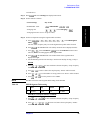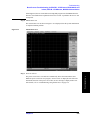
1
Agilent E5070B/E5071B ENA Series RF Network Analyzers
Service Guide
Eighth Edition
Manufacturing No. E5070-90370
November 2008
Notices
The information contained in this document is subject to change without notice.
This document contains proprietary information that is protected by copyright. All rights
are reserved. No part of this document may be photocopied, reproduced, or translated into
another language without the prior written consent of the Agilent Technologies.
Microsoft®,MS-DOS®,Windows®,Visual C++®,Visual Basic®,VBA® and Excel® are
registered
UNIX is a registered trademark in U.S. and other countries, licensed
exclusively through X/Open Company Limited.
Portions ©Copyright 1996, Microsoft Corporation. All rights reserved.
© Copyright 2005, 2007, 2008 Agilent Technologies
Manual Printing History
The manual’s printing date and part number indicate its current edition. The printing date
changes when a new edition is printed. (Minor corrections and updates that are
incorporated at reprint do not cause the date to change.) The manual part number changes
when extensive technical changes are incorporated.
October 2002
First Edition
March 2003
Second Edition
November 2004
Third Edition (Update service information for serial prefix MY422,
and the A20 motherboard change.)
May 2005
Fourth Edition (Added removable HDD and USB (USBTMC)
interface port for serial prefix MY424 and above.)
November 2005
Fifth Edition
May 2006
Sixth Edition
February 2007
Seventh Edition
November 2008
Eighth Edition
2
Safety Summary
The following general safety precautions must be observed during all phases of operation,
service, and repair of this instrument. Failure to comply with these precautions or with
specific WARNINGS elsewhere in this manual may impair the protection provided by the
equipment. In addition it violates safety standards of design, manufacture, and intended use
of the instrument.
Agilent Technologies assumes no liability for the customer’s failure to comply with these
requirements.
NOTE
E5070B/E5071B comply with INSTALLATION CATEGORY II and POLLUTION
DEGREE 2 in IEC61010-1. E5070B/E5071B are INDOOR USE product.
NOTE
LEDs in E5070B/E5071B are Class 1 in accordance with IEC60825-1.
CLASS 1 LED PRODUCT
NOTE
This equipment is MEASUREMENT CATEGORY I (CAT I). Do not use for CAT II, III,
or IV.
NOTE
This equipment is tested with stand-alone condition or with the combination with the
accessories supplied by Agilent Technologies against the requirement of the standards
described in the Declaration of Conformity. If it is used as a system component,
compliance of related regulations and safety requirements are to be confirmed by the
builder of the system.
•
Ground The Instrument
To avoid electric shock hazard, the instrument chassis and cabinet must be connected
to a safety earth ground by the supplied power cable with earth blade.
•
DO NOT Operate In An Explosive Atmosphere
Do not operate the instrument in the presence of flammable gasses or fumes. Operation
of any electrical instrument in such an environment constitutes a definite safety hazard.
•
Keep Away From Live Circuits
Operating personnel must not remove instrument covers. Component replacement and
internal adjustments must be made by qualified maintenance personnel. Do not replace
components with the power cable connected. Under certain conditions, dangerous
voltages may exist even with the power cable removed. To avoid injuries, always
disconnect power and discharge circuits before touching them.
•
DO NOT Service Or Adjust Alone
Do not attempt internal service or adjustment unless another person, capable of
rendering first aid and resuscitation, is present.
•
DO NOT Substitute Parts Or Modify Instrument
Because of the danger of introducing additional hazards, do not install substitute parts
or perform unauthorized modifications to the instrument. Return the instrument to a
Agilent Technologies Sales and Service Office for service and repair to ensure that
3
safety features are maintained.
•
Dangerous Procedure Warnings
Warnings, such as the example below, precede potentially dangerous procedures
throughout this manual. Instructions contained in the warnings must be followed.
WARNING
Dangerous voltages, capable of causing death, are presenting this instrument. Use
extreme caution when handling, testing, and adjusting this instrument.
Safety Symbol
General definitions of safety symbols used on the instrument or in manuals are listed
below.
Instruction Manual symbol: the product is marked with this symbol when it is necessary for
the user to refer to the instrument manual.
Alternating current.
Direct current.
On (Supply).
Off (Supply).
In position of push-button switch.
Out position of push-button switch.
Frame (or chassis) terminal. A connection to the frame (chassis) of the equipment which
normally include all exposed metal structure.
Stand-by.
WARNING
This warning sign denotes a hazard. It calls attention to a procedure, practice,
condition or the like, which, if not correctly performed or adhered to, could result in
injury or death to personnel.
CAUTION
This Caution sign denotes a hazard. It calls attention to a procedure, practice, condition or
the like, which, if not correctly performed or adhered to, could result in damage to or
destruction of part or all of the product.
NOTE
Note denotes important information. It calls attention to a procedure, practice, condition or
the like, which is essential to highlight.
4
Certification
Agilent Technologies certifies that this product met its published specifications at the time
of shipment from the factory. Agilent Technologies further certifies that its calibration
measurements are traceable to the United States National Institute of Standards and
Technology, to the extent allowed by the Institution’s calibration facility, or to the
calibration facilities of other International Standards Organization members.
Documentation Warranty
The material contained in this document is provided "as is," and is subject to being
changed, without notice, in future editions. Further, to the maximum extent permitted by
applicable law, Agilent disclaims all warranties, either express or implied with regard to
this manual and any information contained herein, including but not limited to the implied
warranties of merchantability and fitness for a particular purpose. Agilent shall not be
liable for errors or for incidental or consequential damages in connection with the
furnishing, use, or performance of this document or any information contained herein.
Should Agilent and the user have a separate written agreement with warranty terms
covering the material in this document that conflict with these terms, the warranty terms in
the separate agreement will control.
Exclusive Remedies
The remedies provided herein are buyer’s sole and exclusive remedies. Agilent
Technologies shall not be liable for any direct, indirect, special, incidental, or
consequential damages, whether based on contract, tort, or any other legal theory.
Assistance
Product maintenance agreements and other customer assistance agreements are available
for Agilent Technologies products.
For any assistance, contact your nearest Agilent Technologies Sales and Service Office.
Addresses are provided at the back of this manual.
5
Typeface Conventions
Sample (bold)
Boldface type is used when a term is defined or
emphasised.
Sample (Italic)
Italic type is used for emphasis.
key / [Sample] key
Indicates a hardkey (key on the front panel or
external keyboard) labeled “Sample.” “key” may
be omitted.
Sample menu/button/box
Indicates a menu/button/box on the screen labeled
“Sample” which can be selected/executed by
clicking. “menu,” “button,” or “box” may be
omitted.
Sample block/toolbar
Indicates a block (group of hardkeys) or a toolbar
(setup toolbar) labeled “Sample.”
Sample 1 - Sample 2 - Sample 3
Indicates a sequential operation of Sample 1,
Sample 2, and Sample 3 (menu, button, or box).
“-” may be omitted.
6
Contents
1. General Information
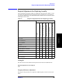
Precautions . . . . . . . . . . . . . . . . . . . . . . . . . . . . . . . . . . . . . . . . . . . . . . . . . . . . . . . . . . . . . . . . . . . . . . . . . . 20
Software Installed . . . . . . . . . . . . . . . . . . . . . . . . . . . . . . . . . . . . . . . . . . . . . . . . . . . . . . . . . . . . . . . . . . . 20
Organization of Service Manual . . . . . . . . . . . . . . . . . . . . . . . . . . . . . . . . . . . . . . . . . . . . . . . . . . . . . . . . . . 21
Instrument Covered by This Manual . . . . . . . . . . . . . . . . . . . . . . . . . . . . . . . . . . . . . . . . . . . . . . . . . . . . . . 23
Required Equipment . . . . . . . . . . . . . . . . . . . . . . . . . . . . . . . . . . . . . . . . . . . . . . . . . . . . . . . . . . . . . . . . . . . 24
Power Meter Accuracy Test . . . . . . . . . . . . . . . . . . . . . . . . . . . . . . . . . . . . . . . . . . . . . . . . . . . . . . . . . . . . . 26
Power Meters That Can Be Tested Using This Procedure . . . . . . . . . . . . . . . . . . . . . . . . . . . . . . . . . . . . 26
Equipment Used for the Power Meter Accuracy Test. . . . . . . . . . . . . . . . . . . . . . . . . . . . . . . . . . . . . . . . 26
Description of the Test . . . . . . . . . . . . . . . . . . . . . . . . . . . . . . . . . . . . . . . . . . . . . . . . . . . . . . . . . . . . . . . 26
TEST RECORD FOR POWER METER ACCURACY TEST . . . . . . . . . . . . . . . . . . . . . . . . . . . . . . . . 30
2. Performance Tests
Introduction. . . . . . . . . . . . . . . . . . . . . . . . . . . . . . . . . . . . . . . . . . . . . . . . . . . . . . . . . . . . . . . . . . . . . . . . . . 32
Test Equipment Required . . . . . . . . . . . . . . . . . . . . . . . . . . . . . . . . . . . . . . . . . . . . . . . . . . . . . . . . . . . . . 33
Softkey Selection Procedure for Performance Test. . . . . . . . . . . . . . . . . . . . . . . . . . . . . . . . . . . . . . . . . . 33
1. FREQUENCY ACCURACY TEST. . . . . . . . . . . . . . . . . . . . . . . . . . . . . . . . . . . . . . . . . . . . . . . . . . . . . 34
Description . . . . . . . . . . . . . . . . . . . . . . . . . . . . . . . . . . . . . . . . . . . . . . . . . . . . . . . . . . . . . . . . . . . . . . . . 34
Specification . . . . . . . . . . . . . . . . . . . . . . . . . . . . . . . . . . . . . . . . . . . . . . . . . . . . . . . . . . . . . . . . . . . . . . . 34
Test equipment . . . . . . . . . . . . . . . . . . . . . . . . . . . . . . . . . . . . . . . . . . . . . . . . . . . . . . . . . . . . . . . . . . . . . 34
Procedure. . . . . . . . . . . . . . . . . . . . . . . . . . . . . . . . . . . . . . . . . . . . . . . . . . . . . . . . . . . . . . . . . . . . . . . . . . 34
2. RF OUTPUT LEVEL ACCURACY AND FLATNESS TEST . . . . . . . . . . . . . . . . . . . . . . . . . . . . . . . . 37
Description . . . . . . . . . . . . . . . . . . . . . . . . . . . . . . . . . . . . . . . . . . . . . . . . . . . . . . . . . . . . . . . . . . . . . . . . 37
Specification . . . . . . . . . . . . . . . . . . . . . . . . . . . . . . . . . . . . . . . . . . . . . . . . . . . . . . . . . . . . . . . . . . . . . . . 37
Test equipment . . . . . . . . . . . . . . . . . . . . . . . . . . . . . . . . . . . . . . . . . . . . . . . . . . . . . . . . . . . . . . . . . . . . . 37
Procedure. . . . . . . . . . . . . . . . . . . . . . . . . . . . . . . . . . . . . . . . . . . . . . . . . . . . . . . . . . . . . . . . . . . . . . . . . . 37
3. RF OUTPUT LEVEL LINEARITY TEST . . . . . . . . . . . . . . . . . . . . . . . . . . . . . . . . . . . . . . . . . . . . . . . 40
Description . . . . . . . . . . . . . . . . . . . . . . . . . . . . . . . . . . . . . . . . . . . . . . . . . . . . . . . . . . . . . . . . . . . . . . . . 40
Specification . . . . . . . . . . . . . . . . . . . . . . . . . . . . . . . . . . . . . . . . . . . . . . . . . . . . . . . . . . . . . . . . . . . . . . . 40
Test equipment . . . . . . . . . . . . . . . . . . . . . . . . . . . . . . . . . . . . . . . . . . . . . . . . . . . . . . . . . . . . . . . . . . . . . 41
Procedure. . . . . . . . . . . . . . . . . . . . . . . . . . . . . . . . . . . . . . . . . . . . . . . . . . . . . . . . . . . . . . . . . . . . . . . . . . 41
4. TRACE NOISE CW TEST . . . . . . . . . . . . . . . . . . . . . . . . . . . . . . . . . . . . . . . . . . . . . . . . . . . . . . . . . . . 44
Description . . . . . . . . . . . . . . . . . . . . . . . . . . . . . . . . . . . . . . . . . . . . . . . . . . . . . . . . . . . . . . . . . . . . . . . . 44
Specification . . . . . . . . . . . . . . . . . . . . . . . . . . . . . . . . . . . . . . . . . . . . . . . . . . . . . . . . . . . . . . . . . . . . . . . 44
Test equipment . . . . . . . . . . . . . . . . . . . . . . . . . . . . . . . . . . . . . . . . . . . . . . . . . . . . . . . . . . . . . . . . . . . . . 44
Procedure. . . . . . . . . . . . . . . . . . . . . . . . . . . . . . . . . . . . . . . . . . . . . . . . . . . . . . . . . . . . . . . . . . . . . . . . . . 45
5. CROSSTALK TEST . . . . . . . . . . . . . . . . . . . . . . . . . . . . . . . . . . . . . . . . . . . . . . . . . . . . . . . . . . . . . . . . . 50
Description . . . . . . . . . . . . . . . . . . . . . . . . . . . . . . . . . . . . . . . . . . . . . . . . . . . . . . . . . . . . . . . . . . . . . . . . 50
Specification . . . . . . . . . . . . . . . . . . . . . . . . . . . . . . . . . . . . . . . . . . . . . . . . . . . . . . . . . . . . . . . . . . . . . . . 50
Test equipment . . . . . . . . . . . . . . . . . . . . . . . . . . . . . . . . . . . . . . . . . . . . . . . . . . . . . . . . . . . . . . . . . . . . . 51
Procedure. . . . . . . . . . . . . . . . . . . . . . . . . . . . . . . . . . . . . . . . . . . . . . . . . . . . . . . . . . . . . . . . . . . . . . . . . . 51
Crosstalk test program. . . . . . . . . . . . . . . . . . . . . . . . . . . . . . . . . . . . . . . . . . . . . . . . . . . . . . . . . . . . . . . . 60
6. SYSTEM DYNAMIC RANGE TEST . . . . . . . . . . . . . . . . . . . . . . . . . . . . . . . . . . . . . . . . . . . . . . . . . . . 63
Description . . . . . . . . . . . . . . . . . . . . . . . . . . . . . . . . . . . . . . . . . . . . . . . . . . . . . . . . . . . . . . . . . . . . . . . . 63
Specification . . . . . . . . . . . . . . . . . . . . . . . . . . . . . . . . . . . . . . . . . . . . . . . . . . . . . . . . . . . . . . . . . . . . . . . 63
Test equipment . . . . . . . . . . . . . . . . . . . . . . . . . . . . . . . . . . . . . . . . . . . . . . . . . . . . . . . . . . . . . . . . . . . . . 64
Procedure. . . . . . . . . . . . . . . . . . . . . . . . . . . . . . . . . . . . . . . . . . . . . . . . . . . . . . . . . . . . . . . . . . . . . . . . . . 64
System Dynamic Range test program . . . . . . . . . . . . . . . . . . . . . . . . . . . . . . . . . . . . . . . . . . . . . . . . . . . . 77
7. DYNAMIC ACCURACY TEST . . . . . . . . . . . . . . . . . . . . . . . . . . . . . . . . . . . . . . . . . . . . . . . . . . . . . . . 82
7
Contents
Description . . . . . . . . . . . . . . . . . . . . . . . . . . . . . . . . . . . . . . . . . . . . . . . . . . . . . . . . . . . . . . . . . . . . . . . . 82
Test Equipment . . . . . . . . . . . . . . . . . . . . . . . . . . . . . . . . . . . . . . . . . . . . . . . . . . . . . . . . . . . . . . . . . . . . . 82
Procedure . . . . . . . . . . . . . . . . . . . . . . . . . . . . . . . . . . . . . . . . . . . . . . . . . . . . . . . . . . . . . . . . . . . . . . . . . 83
8. UNCORRECTED SYSTEM PERFORMANCE TEST. . . . . . . . . . . . . . . . . . . . . . . . . . . . . . . . . . . . . . 97
Description . . . . . . . . . . . . . . . . . . . . . . . . . . . . . . . . . . . . . . . . . . . . . . . . . . . . . . . . . . . . . . . . . . . . . . . . 97
Specification . . . . . . . . . . . . . . . . . . . . . . . . . . . . . . . . . . . . . . . . . . . . . . . . . . . . . . . . . . . . . . . . . . . . . . . 97
Test Equipment . . . . . . . . . . . . . . . . . . . . . . . . . . . . . . . . . . . . . . . . . . . . . . . . . . . . . . . . . . . . . . . . . . . . . 97
Procedure . . . . . . . . . . . . . . . . . . . . . . . . . . . . . . . . . . . . . . . . . . . . . . . . . . . . . . . . . . . . . . . . . . . . . . . . . 97
E5070B/E5071B Performance Test Calculation Sheet . . . . . . . . . . . . . . . . . . . . . . . . . . . . . . . . . . . . . . . 116
Introduction. . . . . . . . . . . . . . . . . . . . . . . . . . . . . . . . . . . . . . . . . . . . . . . . . . . . . . . . . . . . . . . . . . . . . . . 116
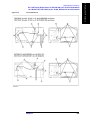
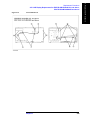
2. RF Output Level Accuracy and Flatness Test. . . . . . . . . . . . . . . . . . . . . . . . . . . . . . . . . . . . . . . . . . . 116
3. RF Output Level Linearity Test . . . . . . . . . . . . . . . . . . . . . . . . . . . . . . . . . . . . . . . . . . . . . . . . . . . . . 117
4. Trace Noise CW Test . . . . . . . . . . . . . . . . . . . . . . . . . . . . . . . . . . . . . . . . . . . . . . . . . . . . . . . . . . . . . 125
7. Dynamic Accuracy Test . . . . . . . . . . . . . . . . . . . . . . . . . . . . . . . . . . . . . . . . . . . . . . . . . . . . . . . . . . . 127
E5070B Performance Test Record for Serial Prefix: MY421, or JP1KK . . . . . . . . . . . . . . . . . . . . . . . . . 130
Frequency Accuracy Test . . . . . . . . . . . . . . . . . . . . . . . . . . . . . . . . . . . . . . . . . . . . . . . . . . . . . . . . . . . . 130
RF Output Level Accuracy and Flatness Test. . . . . . . . . . . . . . . . . . . . . . . . . . . . . . . . . . . . . . . . . . . . . 130
RF Output Level Linearity Test (@ Port1) . . . . . . . . . . . . . . . . . . . . . . . . . . . . . . . . . . . . . . . . . . . . . . . 131
Trace Noise CW Test (Magnitude) . . . . . . . . . . . . . . . . . . . . . . . . . . . . . . . . . . . . . . . . . . . . . . . . . . . . 133
Crosstalk Test . . . . . . . . . . . . . . . . . . . . . . . . . . . . . . . . . . . . . . . . . . . . . . . . . . . . . . . . . . . . . . . . . . . . . 134
System Dynamic Range Test . . . . . . . . . . . . . . . . . . . . . . . . . . . . . . . . . . . . . . . . . . . . . . . . . . . . . . . . . 135
Dynamic Accuracy Test . . . . . . . . . . . . . . . . . . . . . . . . . . . . . . . . . . . . . . . . . . . . . . . . . . . . . . . . . . . . . 136
Uncorrected System Performance Test. . . . . . . . . . . . . . . . . . . . . . . . . . . . . . . . . . . . . . . . . . . . . . . . . . 140
E5070B Performance Test Record for Serial Prefix: MY422, and above . . . . . . . . . . . . . . . . . . . . . . . . . 142
Frequency Accuracy Test . . . . . . . . . . . . . . . . . . . . . . . . . . . . . . . . . . . . . . . . . . . . . . . . . . . . . . . . . . . . 142
RF Output Level Accuracy and Flatness Test. . . . . . . . . . . . . . . . . . . . . . . . . . . . . . . . . . . . . . . . . . . . . 142
RF Output Level Linearity Test (@ Port1) . . . . . . . . . . . . . . . . . . . . . . . . . . . . . . . . . . . . . . . . . . . . . . . 143
Trace Noise CW Test (Magnitude) . . . . . . . . . . . . . . . . . . . . . . . . . . . . . . . . . . . . . . . . . . . . . . . . . . . . 145
Crosstalk Test . . . . . . . . . . . . . . . . . . . . . . . . . . . . . . . . . . . . . . . . . . . . . . . . . . . . . . . . . . . . . . . . . . . . . 146
System Dynamic Range Test . . . . . . . . . . . . . . . . . . . . . . . . . . . . . . . . . . . . . . . . . . . . . . . . . . . . . . . . . 147
Dynamic Accuracy Test . . . . . . . . . . . . . . . . . . . . . . . . . . . . . . . . . . . . . . . . . . . . . . . . . . . . . . . . . . . . . 148
Uncorrected System Performance Test. . . . . . . . . . . . . . . . . . . . . . . . . . . . . . . . . . . . . . . . . . . . . . . . . . 152
E5071B Performance Test Record for Serial Prefix: MY421, or JP1KK . . . . . . . . . . . . . . . . . . . . . . . . . 154
Frequency Accuracy Test . . . . . . . . . . . . . . . . . . . . . . . . . . . . . . . . . . . . . . . . . . . . . . . . . . . . . . . . . . . . 154
RF Output Level Accuracy and Flatness Test. . . . . . . . . . . . . . . . . . . . . . . . . . . . . . . . . . . . . . . . . . . . . 154
RF Output Level Linearity Test (@ Port1) . . . . . . . . . . . . . . . . . . . . . . . . . . . . . . . . . . . . . . . . . . . . . . . 155
Trace Noise CW Test (Magnitude) . . . . . . . . . . . . . . . . . . . . . . . . . . . . . . . . . . . . . . . . . . . . . . . . . . . . 160
Crosstalk Test . . . . . . . . . . . . . . . . . . . . . . . . . . . . . . . . . . . . . . . . . . . . . . . . . . . . . . . . . . . . . . . . . . . . . 162
System Dynamic Range Test . . . . . . . . . . . . . . . . . . . . . . . . . . . . . . . . . . . . . . . . . . . . . . . . . . . . . . . . . 163
Dynamic Accuracy Test . . . . . . . . . . . . . . . . . . . . . . . . . . . . . . . . . . . . . . . . . . . . . . . . . . . . . . . . . . . . . 166
Uncorrected System Performance Test. . . . . . . . . . . . . . . . . . . . . . . . . . . . . . . . . . . . . . . . . . . . . . . . . . 169
E5071B Performance Test Record for Serial Prefix: MY422, and above . . . . . . . . . . . . . . . . . . . . . . . . . 173
Frequency Accuracy Test . . . . . . . . . . . . . . . . . . . . . . . . . . . . . . . . . . . . . . . . . . . . . . . . . . . . . . . . . . . . 173
RF Output Level Accuracy and Flatness Test. . . . . . . . . . . . . . . . . . . . . . . . . . . . . . . . . . . . . . . . . . . . . 173
RF Output Level Linearity Test (@ Port1) . . . . . . . . . . . . . . . . . . . . . . . . . . . . . . . . . . . . . . . . . . . . . . . 174
Trace Noise CW Test (Magnitude) . . . . . . . . . . . . . . . . . . . . . . . . . . . . . . . . . . . . . . . . . . . . . . . . . . . . 179
Crosstalk Test . . . . . . . . . . . . . . . . . . . . . . . . . . . . . . . . . . . . . . . . . . . . . . . . . . . . . . . . . . . . . . . . . . . . . 181
System Dynamic Range Test . . . . . . . . . . . . . . . . . . . . . . . . . . . . . . . . . . . . . . . . . . . . . . . . . . . . . . . . . 182
Dynamic Accuracy Test . . . . . . . . . . . . . . . . . . . . . . . . . . . . . . . . . . . . . . . . . . . . . . . . . . . . . . . . . . . . . 185
8
Contents
Uncorrected System Performance Test . . . . . . . . . . . . . . . . . . . . . . . . . . . . . . . . . . . . . . . . . . . . . . . . . . 189
3. Adjustment
Safety Considerations . . . . . . . . . . . . . . . . . . . . . . . . . . . . . . . . . . . . . . . . . . . . . . . . . . . . . . . . . . . . . . . . . 194
Warm-up for Adjustment . . . . . . . . . . . . . . . . . . . . . . . . . . . . . . . . . . . . . . . . . . . . . . . . . . . . . . . . . . . . . . 194
Required Equipment . . . . . . . . . . . . . . . . . . . . . . . . . . . . . . . . . . . . . . . . . . . . . . . . . . . . . . . . . . . . . . . . . . 194
Required Adjustment after Replacing Assembly . . . . . . . . . . . . . . . . . . . . . . . . . . . . . . . . . . . . . . . . . . . . 195
Writing ID . . . . . . . . . . . . . . . . . . . . . . . . . . . . . . . . . . . . . . . . . . . . . . . . . . . . . . . . . . . . . . . . . . . . . . . . 195
Frequency Reference Adjustment . . . . . . . . . . . . . . . . . . . . . . . . . . . . . . . . . . . . . . . . . . . . . . . . . . . . . . 195
Oven Reference Adjustment . . . . . . . . . . . . . . . . . . . . . . . . . . . . . . . . . . . . . . . . . . . . . . . . . . . . . . . . . . 196
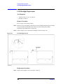
IF Range Gain/Phase Adjustment . . . . . . . . . . . . . . . . . . . . . . . . . . . . . . . . . . . . . . . . . . . . . . . . . . . . . . 196
Source Power Adjustment. . . . . . . . . . . . . . . . . . . . . . . . . . . . . . . . . . . . . . . . . . . . . . . . . . . . . . . . . . . . 196
Test Ports Characteristics Adjustment. . . . . . . . . . . . . . . . . . . . . . . . . . . . . . . . . . . . . . . . . . . . . . . . . . . 197
4. Troubleshooting
Introduction. . . . . . . . . . . . . . . . . . . . . . . . . . . . . . . . . . . . . . . . . . . . . . . . . . . . . . . . . . . . . . . . . . . . . . . . . 200
How to exit from the E5070B/E5071B Measurement View . . . . . . . . . . . . . . . . . . . . . . . . . . . . . . . . . . . 201
To Troubleshoot the Instrument . . . . . . . . . . . . . . . . . . . . . . . . . . . . . . . . . . . . . . . . . . . . . . . . . . . . . . . . . 202
Primary Trouble Isolation . . . . . . . . . . . . . . . . . . . . . . . . . . . . . . . . . . . . . . . . . . . . . . . . . . . . . . . . . . . . 202
No Display troubleshooting . . . . . . . . . . . . . . . . . . . . . . . . . . . . . . . . . . . . . . . . . . . . . . . . . . . . . . . . . . . . 204
Boot Process Troubleshooting for E5070B : JP1KKxxxxx, MY42300632 and below, E5071B :
JP1KKxxxxx, MY42301396 and below . . . . . . . . . . . . . . . . . . . . . . . . . . . . . . . . . . . . . . . . . . . . . . . . . . . 207
Boot Process Troubleshooting for E5070B : MY42300633 and above, E5071B : MY42301397 and above .
214
Troubleshooting Using Internal Test. . . . . . . . . . . . . . . . . . . . . . . . . . . . . . . . . . . . . . . . . . . . . . . . . . . . . . 219
Power On Self Test . . . . . . . . . . . . . . . . . . . . . . . . . . . . . . . . . . . . . . . . . . . . . . . . . . . . . . . . . . . . . . . . . 219
PLL unlock . . . . . . . . . . . . . . . . . . . . . . . . . . . . . . . . . . . . . . . . . . . . . . . . . . . . . . . . . . . . . . . . . . . . . . . 219
External reference signal phase unlock (Opt. 1E5). . . . . . . . . . . . . . . . . . . . . . . . . . . . . . . . . . . . . . . . . 219
To Execute the Internal Test . . . . . . . . . . . . . . . . . . . . . . . . . . . . . . . . . . . . . . . . . . . . . . . . . . . . . . . . . . 219
Internal Test Failure Troubleshooting . . . . . . . . . . . . . . . . . . . . . . . . . . . . . . . . . . . . . . . . . . . . . . . . . . . 222
Function Specific Troubleshooting. . . . . . . . . . . . . . . . . . . . . . . . . . . . . . . . . . . . . . . . . . . . . . . . . . . . . . . 227
To Check the Device Driver . . . . . . . . . . . . . . . . . . . . . . . . . . . . . . . . . . . . . . . . . . . . . . . . . . . . . . . . . . 228
To Check the Front Panel . . . . . . . . . . . . . . . . . . . . . . . . . . . . . . . . . . . . . . . . . . . . . . . . . . . . . . . . . . . . 230
To Check the Touch Panel (Option 016 only). . . . . . . . . . . . . . . . . . . . . . . . . . . . . . . . . . . . . . . . . . . . . 231
To Check the LCD. . . . . . . . . . . . . . . . . . . . . . . . . . . . . . . . . . . . . . . . . . . . . . . . . . . . . . . . . . . . . . . . . . 231
To Check the External Keyboard . . . . . . . . . . . . . . . . . . . . . . . . . . . . . . . . . . . . . . . . . . . . . . . . . . . . . . 232
To Check the Mouse . . . . . . . . . . . . . . . . . . . . . . . . . . . . . . . . . . . . . . . . . . . . . . . . . . . . . . . . . . . . . . . . 232
To Check the FDD. . . . . . . . . . . . . . . . . . . . . . . . . . . . . . . . . . . . . . . . . . . . . . . . . . . . . . . . . . . . . . . . . . 232
To Check the Video output . . . . . . . . . . . . . . . . . . . . . . . . . . . . . . . . . . . . . . . . . . . . . . . . . . . . . . . . . . . 233
To Check the External Trigger Input. . . . . . . . . . . . . . . . . . . . . . . . . . . . . . . . . . . . . . . . . . . . . . . . . . . . 233
To Check the LAN . . . . . . . . . . . . . . . . . . . . . . . . . . . . . . . . . . . . . . . . . . . . . . . . . . . . . . . . . . . . . . . . . 233
To Check the Printer Parallel Port. . . . . . . . . . . . . . . . . . . . . . . . . . . . . . . . . . . . . . . . . . . . . . . . . . . . . . 237
To Check the GPIB . . . . . . . . . . . . . . . . . . . . . . . . . . . . . . . . . . . . . . . . . . . . . . . . . . . . . . . . . . . . . . . . . 238
To Check the USB (USBTMC) Interface Card. . . . . . . . . . . . . . . . . . . . . . . . . . . . . . . . . . . . . . . . . . . . 238
Troubleshooting Using External Test . . . . . . . . . . . . . . . . . . . . . . . . . . . . . . . . . . . . . . . . . . . . . . . . . . . . . 239
Contents of the external test . . . . . . . . . . . . . . . . . . . . . . . . . . . . . . . . . . . . . . . . . . . . . . . . . . . . . . . . . . 239
Test equipment required for external test . . . . . . . . . . . . . . . . . . . . . . . . . . . . . . . . . . . . . . . . . . . . . . . . 239
To Execute the External Test. . . . . . . . . . . . . . . . . . . . . . . . . . . . . . . . . . . . . . . . . . . . . . . . . . . . . . . . . . 240
9
Contents
External Test Failure Troubleshooting . . . . . . . . . . . . . . . . . . . . . . . . . . . . . . . . . . . . . . . . . . . . . . . . . . 254
Performance test failure troubleshooting . . . . . . . . . . . . . . . . . . . . . . . . . . . . . . . . . . . . . . . . . . . . . . . . . . 260
Recommended adjustment for performance test failure . . . . . . . . . . . . . . . . . . . . . . . . . . . . . . . . . . . . . 260
Performance test failure troubleshooting . . . . . . . . . . . . . . . . . . . . . . . . . . . . . . . . . . . . . . . . . . . . . . . . 260
To configure the A20 Digital Motherboard and BIOS for E5070B : JP1KKxxxxx, MY42300632 and below,
E5071B : JP1KKxxxxx, MY42301396 and below . . . . . . . . . . . . . . . . . . . . . . . . . . . . . . . . . . . . . . . . . . 262
To Identify the Motherboard Installed . . . . . . . . . . . . . . . . . . . . . . . . . . . . . . . . . . . . . . . . . . . . . . . . . . 262
Configure the Motherboard . . . . . . . . . . . . . . . . . . . . . . . . . . . . . . . . . . . . . . . . . . . . . . . . . . . . . . . . . . 262
Testing DRAM on the Motherboard . . . . . . . . . . . . . . . . . . . . . . . . . . . . . . . . . . . . . . . . . . . . . . . . . . . . 263
To Confirm or Set the BIOS Options . . . . . . . . . . . . . . . . . . . . . . . . . . . . . . . . . . . . . . . . . . . . . . . . . . . 264
To configure the A20 Digital Motherboard and BIOS for E5070B : MY42300633 and above, E5071B :
MY42301397 and above . . . . . . . . . . . . . . . . . . . . . . . . . . . . . . . . . . . . . . . . . . . . . . . . . . . . . . . . . . . . . . 279
To Identify the Motherboard Installed . . . . . . . . . . . . . . . . . . . . . . . . . . . . . . . . . . . . . . . . . . . . . . . . . . 279
Configure the Motherboard . . . . . . . . . . . . . . . . . . . . . . . . . . . . . . . . . . . . . . . . . . . . . . . . . . . . . . . . . . 279
Testing DRAM on the Motherboard . . . . . . . . . . . . . . . . . . . . . . . . . . . . . . . . . . . . . . . . . . . . . . . . . . . . 279
To Confirm or Set the BIOS Options . . . . . . . . . . . . . . . . . . . . . . . . . . . . . . . . . . . . . . . . . . . . . . . . . . . 280
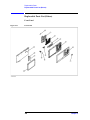
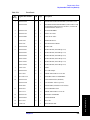
5. Replaceable Parts
Ordering Information . . . . . . . . . . . . . . . . . . . . . . . . . . . . . . . . . . . . . . . . . . . . . . . . . . . . . . . . . . . . . . . . . 288
Direct Mail Order System. . . . . . . . . . . . . . . . . . . . . . . . . . . . . . . . . . . . . . . . . . . . . . . . . . . . . . . . . . . . 288
Exchange Assemblies. . . . . . . . . . . . . . . . . . . . . . . . . . . . . . . . . . . . . . . . . . . . . . . . . . . . . . . . . . . . . . . . . 289
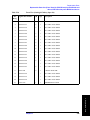
Replaceable Parts List (Top View) for E5070B : JP1KKxxxxx, MY42300632 and below, E5071B :
JP1KKxxxxx, MY42301396 and below. . . . . . . . . . . . . . . . . . . . . . . . . . . . . . . . . . . . . . . . . . . . . . . . . . . 290
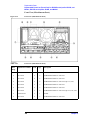
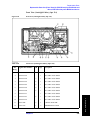
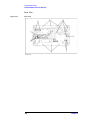
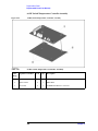
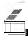
Top View (Major Assemblies) . . . . . . . . . . . . . . . . . . . . . . . . . . . . . . . . . . . . . . . . . . . . . . . . . . . . . . . . 290
Top View (Cables) . . . . . . . . . . . . . . . . . . . . . . . . . . . . . . . . . . . . . . . . . . . . . . . . . . . . . . . . . . . . . . . . . 292
Top View (Miscellaneous Parts) . . . . . . . . . . . . . . . . . . . . . . . . . . . . . . . . . . . . . . . . . . . . . . . . . . . . . . . 294
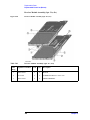
Top View (Under Power Supply) . . . . . . . . . . . . . . . . . . . . . . . . . . . . . . . . . . . . . . . . . . . . . . . . . . . . . . 296
Top View (Motherboard and Other Parts) . . . . . . . . . . . . . . . . . . . . . . . . . . . . . . . . . . . . . . . . . . . . . . . 298
Replaceable Parts List (Top View) for E5070B : MY42300633 and above, E5071B : MY42301397 and above
(A27 mass storage disk drive model) . . . . . . . . . . . . . . . . . . . . . . . . . . . . . . . . . . . . . . . . . . . . . . . . . . . . . 300
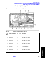
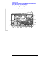
Top View (Major Assemblies) . . . . . . . . . . . . . . . . . . . . . . . . . . . . . . . . . . . . . . . . . . . . . . . . . . . . . . . . 300
Top View (Cables) . . . . . . . . . . . . . . . . . . . . . . . . . . . . . . . . . . . . . . . . . . . . . . . . . . . . . . . . . . . . . . . . . 302
Top View (Miscellaneous Parts) . . . . . . . . . . . . . . . . . . . . . . . . . . . . . . . . . . . . . . . . . . . . . . . . . . . . . . . 304
Top View (Under Power Supply) . . . . . . . . . . . . . . . . . . . . . . . . . . . . . . . . . . . . . . . . . . . . . . . . . . . . . . 306
Top View (Motherboard and Other Parts) . . . . . . . . . . . . . . . . . . . . . . . . . . . . . . . . . . . . . . . . . . . . . . . 308
Replaceable Parts List (Top View) for E5070B S/N MY42401101 and above, E5071B S/N MY42402455 and
above. . . . . . . . . . . . . . . . . . . . . . . . . . . . . . . . . . . . . . . . . . . . . . . . . . . . . . . . . . . . . . . . . . . . . . . . . . . . . . 310
Top View (Removable Hard Disk Assemblies) . . . . . . . . . . . . . . . . . . . . . . . . . . . . . . . . . . . . . . . . . . . 310
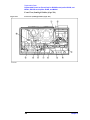
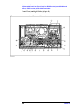
Top View (Major Assemblies) . . . . . . . . . . . . . . . . . . . . . . . . . . . . . . . . . . . . . . . . . . . . . . . . . . . . . . . . 312
Top View (Cables) . . . . . . . . . . . . . . . . . . . . . . . . . . . . . . . . . . . . . . . . . . . . . . . . . . . . . . . . . . . . . . . . . 314
Top View (Miscellaneous Parts) . . . . . . . . . . . . . . . . . . . . . . . . . . . . . . . . . . . . . . . . . . . . . . . . . . . . . . . 316
Top View (Under Power Supply) for E5070B S/N from MY42401101 to MY42401986, E5071B S/N from
MY42402455 to MY42404509 . . . . . . . . . . . . . . . . . . . . . . . . . . . . . . . . . . . . . . . . . . . . . . . . . . . . . . . 318
Top View (Under Power Supply) for E5070B S/N MY42401987 and above, E5071B S/N MY42404510
and above . . . . . . . . . . . . . . . . . . . . . . . . . . . . . . . . . . . . . . . . . . . . . . . . . . . . . . . . . . . . . . . . . . . . . . . . 320
Top View (Motherboard and Other Parts) . . . . . . . . . . . . . . . . . . . . . . . . . . . . . . . . . . . . . . . . . . . . . . . 322
Replaceable Parts List (Front View) for E5070B serial prefix JP1KK, and MY421, E5071B serial prefix
JP1KK, and MY421 . . . . . . . . . . . . . . . . . . . . . . . . . . . . . . . . . . . . . . . . . . . . . . . . . . . . . . . . . . . . . . . . . . 324
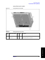
Front View (Analog) . . . . . . . . . . . . . . . . . . . . . . . . . . . . . . . . . . . . . . . . . . . . . . . . . . . . . . . . . . . . . . . 324
10
Contents
Front View (Miscellaneous Parts) . . . . . . . . . . . . . . . . . . . . . . . . . . . . . . . . . . . . . . . . . . . . . . . . . . . . . . 326
Front View (Semirigid Cables) (Opt. 213) . . . . . . . . . . . . . . . . . . . . . . . . . . . . . . . . . . . . . . . . . . . . . . . 327
Front View (Semirigid Cables) (Opt. 214) . . . . . . . . . . . . . . . . . . . . . . . . . . . . . . . . . . . . . . . . . . . . . . . 328
Front View (Semirigid Cables) (Opt. 313) . . . . . . . . . . . . . . . . . . . . . . . . . . . . . . . . . . . . . . . . . . . . . . . 330
Front View (Semirigid Cables) (Opt. 314) . . . . . . . . . . . . . . . . . . . . . . . . . . . . . . . . . . . . . . . . . . . . . . . 332
Front View (Semirigid Cables) (Opt. 413) . . . . . . . . . . . . . . . . . . . . . . . . . . . . . . . . . . . . . . . . . . . . . . . 334
Front View (Semirigid Cables) (Opt. 414) . . . . . . . . . . . . . . . . . . . . . . . . . . . . . . . . . . . . . . . . . . . . . . . 336
Replaceable Parts List (Front View) for E5070B serial prefix MY422 and above, E5071B serial prefix
MY422 and above. . . . . . . . . . . . . . . . . . . . . . . . . . . . . . . . . . . . . . . . . . . . . . . . . . . . . . . . . . . . . . . . . . . . 338
Front View (Analog) . . . . . . . . . . . . . . . . . . . . . . . . . . . . . . . . . . . . . . . . . . . . . . . . . . . . . . . . . . . . . . . 338
Front View (Miscellaneous Parts) . . . . . . . . . . . . . . . . . . . . . . . . . . . . . . . . . . . . . . . . . . . . . . . . . . . . . . 340
Front View (Semirigid Cables) (Opt. 214) . . . . . . . . . . . . . . . . . . . . . . . . . . . . . . . . . . . . . . . . . . . . . . . 341
Front View (Semirigid Cables) (Opt. 314) . . . . . . . . . . . . . . . . . . . . . . . . . . . . . . . . . . . . . . . . . . . . . . . 342
Front View (Semirigid Cables) (Opt. 414) . . . . . . . . . . . . . . . . . . . . . . . . . . . . . . . . . . . . . . . . . . . . . . . 344
Replaceable Parts List (Others) . . . . . . . . . . . . . . . . . . . . . . . . . . . . . . . . . . . . . . . . . . . . . . . . . . . . . . . . . 346
Front Panel . . . . . . . . . . . . . . . . . . . . . . . . . . . . . . . . . . . . . . . . . . . . . . . . . . . . . . . . . . . . . . . . . . . . . . . 346
Rear View . . . . . . . . . . . . . . . . . . . . . . . . . . . . . . . . . . . . . . . . . . . . . . . . . . . . . . . . . . . . . . . . . . . . . . . . 348
Side View . . . . . . . . . . . . . . . . . . . . . . . . . . . . . . . . . . . . . . . . . . . . . . . . . . . . . . . . . . . . . . . . . . . . . . . . 350
Cover Assembly for E5070B serial prefix JP1KK, MY423 and below, E5071B serial prefix JP1KK,
MY423 and below. . . . . . . . . . . . . . . . . . . . . . . . . . . . . . . . . . . . . . . . . . . . . . . . . . . . . . . . . . . . . . . . . . 351
Cover Assembly for E5070B S/N MY42401101 and above, E5071B S/N MY42402455 and above . . 352
A28 FDD Assembly . . . . . . . . . . . . . . . . . . . . . . . . . . . . . . . . . . . . . . . . . . . . . . . . . . . . . . . . . . . . . . . . 353
A27 Mass Storage Disk Drive Assembly for E5070B serial prefix JP1KK, MY423 and below, E5071B
serial prefix JP1KK, MY423 and below . . . . . . . . . . . . . . . . . . . . . . . . . . . . . . . . . . . . . . . . . . . . . . . . . 354
A4 Power Amp. Module Assembly . . . . . . . . . . . . . . . . . . . . . . . . . . . . . . . . . . . . . . . . . . . . . . . . . . . . 356
A8 RF Switch Assembly for E5070B serial prefix JP1KK or MY421, E5071B serial prefix JP1KK or
MY421 . . . . . . . . . . . . . . . . . . . . . . . . . . . . . . . . . . . . . . . . . . . . . . . . . . . . . . . . . . . . . . . . . . . . . . . . . . 357
A8 RF Switch Assembly for E5070B serial prefix MY422 and above, E5071B serial prefix MY422 and
above . . . . . . . . . . . . . . . . . . . . . . . . . . . . . . . . . . . . . . . . . . . . . . . . . . . . . . . . . . . . . . . . . . . . . . . . . . . . 358
A7 Source Step Attenuator Assembly for E5070B serial prefix JP1KK or MY421, E5071B serial prefix
JP1KK or MY421 (Opt. 214, 314, 414) . . . . . . . . . . . . . . . . . . . . . . . . . . . . . . . . . . . . . . . . . . . . . . . . . 359
A7 Source Step Attenuator Assembly for E5070B serial prefix MY422 and above, E5071B serial prefix
MY422 and above (Opt. 214) . . . . . . . . . . . . . . . . . . . . . . . . . . . . . . . . . . . . . . . . . . . . . . . . . . . . . . . . . 360
A7 Source Step Attenuator Assembly for E5070B serial prefix MY422 and above, E5071B serial prefix
MY422 and above (Opt. 314, 414) . . . . . . . . . . . . . . . . . . . . . . . . . . . . . . . . . . . . . . . . . . . . . . . . . . . . . 361
A6 RF Switch/Tempereature Controller Assembly . . . . . . . . . . . . . . . . . . . . . . . . . . . . . . . . . . . . . . . . 362
A2 Receiver Board Assembly . . . . . . . . . . . . . . . . . . . . . . . . . . . . . . . . . . . . . . . . . . . . . . . . . . . . . . . . . 363
Receiver Module Assembly (Opt. 31x, 41x). . . . . . . . . . . . . . . . . . . . . . . . . . . . . . . . . . . . . . . . . . . . . . 364
Analog Motherboard Assembly . . . . . . . . . . . . . . . . . . . . . . . . . . . . . . . . . . . . . . . . . . . . . . . . . . . . . . . 365
Chassis Assembly . . . . . . . . . . . . . . . . . . . . . . . . . . . . . . . . . . . . . . . . . . . . . . . . . . . . . . . . . . . . . . . . . . 366
Keyboard Assembly . . . . . . . . . . . . . . . . . . . . . . . . . . . . . . . . . . . . . . . . . . . . . . . . . . . . . . . . . . . . . . . . 367
LCD and Inverter Assembly for E5060B S/N MY42401986 and below, for E5061B S/N MY42404509 and
below . . . . . . . . . . . . . . . . . . . . . . . . . . . . . . . . . . . . . . . . . . . . . . . . . . . . . . . . . . . . . . . . . . . . . . . . . . . . 368
LCD and Inverter Assembly for E5070B S/N MY42401987 and above, for E5071B S/N MY42404510 and
above . . . . . . . . . . . . . . . . . . . . . . . . . . . . . . . . . . . . . . . . . . . . . . . . . . . . . . . . . . . . . . . . . . . . . . . . . . . . 369
Standby Switch Assembly for E5070B S/N MY42401986 and below, for E5071B S/N MY42404509 and
below . . . . . . . . . . . . . . . . . . . . . . . . . . . . . . . . . . . . . . . . . . . . . . . . . . . . . . . . . . . . . . . . . . . . . . . . . . . . 370
Standby Switch Assembly for E5070B S/N MY42401987 and above, for E5071B S/N MY42404510 and
above . . . . . . . . . . . . . . . . . . . . . . . . . . . . . . . . . . . . . . . . . . . . . . . . . . . . . . . . . . . . . . . . . . . . . . . . . . . . 371
11
Contents
Removable Hard Disk Assemblies for E5070B S/N MY424 1101and above, E5071B S/N MY42402455
and above . . . . . . . . . . . . . . . . . . . . . . . . . . . . . . . . . . . . . . . . . . . . . . . . . . . . . . . . . . . . . . . . . . . . . . . . 372
Cover Assembly (1) . . . . . . . . . . . . . . . . . . . . . . . . . . . . . . . . . . . . . . . . . . . . . . . . . . . . . . . . . . . . . . . . 374
Cover Assembly (2) . . . . . . . . . . . . . . . . . . . . . . . . . . . . . . . . . . . . . . . . . . . . . . . . . . . . . . . . . . . . . . . . 375
Label on Rear Face . . . . . . . . . . . . . . . . . . . . . . . . . . . . . . . . . . . . . . . . . . . . . . . . . . . . . . . . . . . . . . . . . 376
Other Parts . . . . . . . . . . . . . . . . . . . . . . . . . . . . . . . . . . . . . . . . . . . . . . . . . . . . . . . . . . . . . . . . . . . . . . . 377
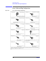
Power Cables and Plug Configurations . . . . . . . . . . . . . . . . . . . . . . . . . . . . . . . . . . . . . . . . . . . . . . . . . . . 378
6. Replacement Procedure
Replacing an Assembly . . . . . . . . . . . . . . . . . . . . . . . . . . . . . . . . . . . . . . . . . . . . . . . . . . . . . . . . . . . . . . .
Required Tools . . . . . . . . . . . . . . . . . . . . . . . . . . . . . . . . . . . . . . . . . . . . . . . . . . . . . . . . . . . . . . . . . . . . . .
Outer Cover Removal. . . . . . . . . . . . . . . . . . . . . . . . . . . . . . . . . . . . . . . . . . . . . . . . . . . . . . . . . . . . . . . . .
Tools Required . . . . . . . . . . . . . . . . . . . . . . . . . . . . . . . . . . . . . . . . . . . . . . . . . . . . . . . . . . . . . . . . . . . .
Procedure . . . . . . . . . . . . . . . . . . . . . . . . . . . . . . . . . . . . . . . . . . . . . . . . . . . . . . . . . . . . . . . . . . . . . . . .
Front Panel Removal for E5070B : JP1KKxxxxx, MY42300632 and below, E5071B : JP1KKxxxxx,
MY42301396 and below . . . . . . . . . . . . . . . . . . . . . . . . . . . . . . . . . . . . . . . . . . . . . . . . . . . . . . . . . . . . . .
Tools required . . . . . . . . . . . . . . . . . . . . . . . . . . . . . . . . . . . . . . . . . . . . . . . . . . . . . . . . . . . . . . . . . . . . .
Procedure . . . . . . . . . . . . . . . . . . . . . . . . . . . . . . . . . . . . . . . . . . . . . . . . . . . . . . . . . . . . . . . . . . . . . . . .
Front Panel Removal for E5070B : MY42300633 thru MY4231100, E5071B : MY42301397 thru
MY4232454 . . . . . . . . . . . . . . . . . . . . . . . . . . . . . . . . . . . . . . . . . . . . . . . . . . . . . . . . . . . . . . . . . . . . . . . .
Tools required . . . . . . . . . . . . . . . . . . . . . . . . . . . . . . . . . . . . . . . . . . . . . . . . . . . . . . . . . . . . . . . . . . . . .
Procedure . . . . . . . . . . . . . . . . . . . . . . . . . . . . . . . . . . . . . . . . . . . . . . . . . . . . . . . . . . . . . . . . . . . . . . . .
Front Panel Removal for E5070B S/N MY42401101 and above, E5071B S/N MY42402455 and above
Tools required . . . . . . . . . . . . . . . . . . . . . . . . . . . . . . . . . . . . . . . . . . . . . . . . . . . . . . . . . . . . . . . . . . . . .
Procedure . . . . . . . . . . . . . . . . . . . . . . . . . . . . . . . . . . . . . . . . . . . . . . . . . . . . . . . . . . . . . . . . . . . . . . . .
A27 Mass Storage Disk Drive Replacement . . . . . . . . . . . . . . . . . . . . . . . . . . . . . . . . . . . . . . . . . . . . . . .
Tools Required . . . . . . . . . . . . . . . . . . . . . . . . . . . . . . . . . . . . . . . . . . . . . . . . . . . . . . . . . . . . . . . . . . . .
Removal Procedure. . . . . . . . . . . . . . . . . . . . . . . . . . . . . . . . . . . . . . . . . . . . . . . . . . . . . . . . . . . . . . . . .
Replacement Procedure . . . . . . . . . . . . . . . . . . . . . . . . . . . . . . . . . . . . . . . . . . . . . . . . . . . . . . . . . . . . .
Restore Backup Files onto the New Mass Storage Disk Drive . . . . . . . . . . . . . . . . . . . . . . . . . . . . . . .
Calibration of the Touch Screen . . . . . . . . . . . . . . . . . . . . . . . . . . . . . . . . . . . . . . . . . . . . . . . . . . . . . . .
Removable Hard Disk Drive Replacement for E5070B S/N MY42401101 and above, for E5071B S/N
MY42402455 and above . . . . . . . . . . . . . . . . . . . . . . . . . . . . . . . . . . . . . . . . . . . . . . . . . . . . . . . . . . . . . .
Tools Required . . . . . . . . . . . . . . . . . . . . . . . . . . . . . . . . . . . . . . . . . . . . . . . . . . . . . . . . . . . . . . . . . . . .
Removal procedure . . . . . . . . . . . . . . . . . . . . . . . . . . . . . . . . . . . . . . . . . . . . . . . . . . . . . . . . . . . . . . . . .
Replacement Procedure . . . . . . . . . . . . . . . . . . . . . . . . . . . . . . . . . . . . . . . . . . . . . . . . . . . . . . . . . . . . .
Restore Backup Files onto the New Removable Hard Disk Drive. . . . . . . . . . . . . . . . . . . . . . . . . . . . .
Calibration of the Touch Screen . . . . . . . . . . . . . . . . . . . . . . . . . . . . . . . . . . . . . . . . . . . . . . . . . . . . . . .
Removable Hard Disk Assembly Removal for E5070B S/N MY42401101 and above, for E5071B S/N
MY42402455 and above . . . . . . . . . . . . . . . . . . . . . . . . . . . . . . . . . . . . . . . . . . . . . . . . . . . . . . . . . . . . . .
Tools Required . . . . . . . . . . . . . . . . . . . . . . . . . . . . . . . . . . . . . . . . . . . . . . . . . . . . . . . . . . . . . . . . . . . .
Removal procedure . . . . . . . . . . . . . . . . . . . . . . . . . . . . . . . . . . . . . . . . . . . . . . . . . . . . . . . . . . . . . . . . .
Replacement Procedure . . . . . . . . . . . . . . . . . . . . . . . . . . . . . . . . . . . . . . . . . . . . . . . . . . . . . . . . . . . . .
A28 FDD (Floppy Disk Drive) Replacement. . . . . . . . . . . . . . . . . . . . . . . . . . . . . . . . . . . . . . . . . . . . . . .
Tools Required . . . . . . . . . . . . . . . . . . . . . . . . . . . . . . . . . . . . . . . . . . . . . . . . . . . . . . . . . . . . . . . . . . . .
Removal procedure . . . . . . . . . . . . . . . . . . . . . . . . . . . . . . . . . . . . . . . . . . . . . . . . . . . . . . . . . . . . . . . . .
Replacement Procedure . . . . . . . . . . . . . . . . . . . . . . . . . . . . . . . . . . . . . . . . . . . . . . . . . . . . . . . . . . . . .
A50 ATX Power Supply Assembly Replacement . . . . . . . . . . . . . . . . . . . . . . . . . . . . . . . . . . . . . . . . . . .
Tools Required . . . . . . . . . . . . . . . . . . . . . . . . . . . . . . . . . . . . . . . . . . . . . . . . . . . . . . . . . . . . . . . . . . . .
12
380
381
382
382
382
384
384
384
386
386
386
388
388
388
390
390
390
390
391
391
392
392
392
393
394
395
396
396
396
396
398
398
398
398
400
400
Contents
Removal Procedure . . . . . . . . . . . . . . . . . . . . . . . . . . . . . . . . . . . . . . . . . . . . . . . . . . . . . . . . . . . . . . . . . 400
Replacement Procedure. . . . . . . . . . . . . . . . . . . . . . . . . . . . . . . . . . . . . . . . . . . . . . . . . . . . . . . . . . . . . . 400
A23 Handler I/O Board Replacement. . . . . . . . . . . . . . . . . . . . . . . . . . . . . . . . . . . . . . . . . . . . . . . . . . . . . 402
Tools Required . . . . . . . . . . . . . . . . . . . . . . . . . . . . . . . . . . . . . . . . . . . . . . . . . . . . . . . . . . . . . . . . . . . . 402
Removal Procedure . . . . . . . . . . . . . . . . . . . . . . . . . . . . . . . . . . . . . . . . . . . . . . . . . . . . . . . . . . . . . . . . . 402
Replacement Procedure. . . . . . . . . . . . . . . . . . . . . . . . . . . . . . . . . . . . . . . . . . . . . . . . . . . . . . . . . . . . . . 402
DIMM Module Replacement for E5070B : JP1KKxxxxx, MY42300632 and below, E5071B : JP1KKxxxxx,
MY42301396 and below . . . . . . . . . . . . . . . . . . . . . . . . . . . . . . . . . . . . . . . . . . . . . . . . . . . . . . . . . . . . . . 404
Tools Required . . . . . . . . . . . . . . . . . . . . . . . . . . . . . . . . . . . . . . . . . . . . . . . . . . . . . . . . . . . . . . . . . . . . 404
Removal Procedure . . . . . . . . . . . . . . . . . . . . . . . . . . . . . . . . . . . . . . . . . . . . . . . . . . . . . . . . . . . . . . . . . 404
Replacement Procedure. . . . . . . . . . . . . . . . . . . . . . . . . . . . . . . . . . . . . . . . . . . . . . . . . . . . . . . . . . . . . . 405
A20 Digital Motherboard Replacement for E5070B : JP1KKxxxxx, MY42300632 and below, E5071B :
JP1KKxxxxx, MY42301396 and below . . . . . . . . . . . . . . . . . . . . . . . . . . . . . . . . . . . . . . . . . . . . . . . . . . . 406
Tools Required . . . . . . . . . . . . . . . . . . . . . . . . . . . . . . . . . . . . . . . . . . . . . . . . . . . . . . . . . . . . . . . . . . . . 406
Removal Procedure . . . . . . . . . . . . . . . . . . . . . . . . . . . . . . . . . . . . . . . . . . . . . . . . . . . . . . . . . . . . . . . . . 406
Replacement Procedure. . . . . . . . . . . . . . . . . . . . . . . . . . . . . . . . . . . . . . . . . . . . . . . . . . . . . . . . . . . . . . 407
A20 Digital Motherboard Replacement for E5070B : MY42300633 thru MY4231100, E5071B :
MY42301397 thru MY4232454 . . . . . . . . . . . . . . . . . . . . . . . . . . . . . . . . . . . . . . . . . . . . . . . . . . . . . . . . . 408
Tools Required . . . . . . . . . . . . . . . . . . . . . . . . . . . . . . . . . . . . . . . . . . . . . . . . . . . . . . . . . . . . . . . . . . . . 408
Removal Procedure . . . . . . . . . . . . . . . . . . . . . . . . . . . . . . . . . . . . . . . . . . . . . . . . . . . . . . . . . . . . . . . . . 408
Replacement Procedure. . . . . . . . . . . . . . . . . . . . . . . . . . . . . . . . . . . . . . . . . . . . . . . . . . . . . . . . . . . . . . 409
A20 Digital Motherboard Replacement for E5070B S/N MY42401101 and above, E5071B S/N
MY42402455 and above. . . . . . . . . . . . . . . . . . . . . . . . . . . . . . . . . . . . . . . . . . . . . . . . . . . . . . . . . . . . . . . 410
Tools Required . . . . . . . . . . . . . . . . . . . . . . . . . . . . . . . . . . . . . . . . . . . . . . . . . . . . . . . . . . . . . . . . . . . . 410
Removal Procedure . . . . . . . . . . . . . . . . . . . . . . . . . . . . . . . . . . . . . . . . . . . . . . . . . . . . . . . . . . . . . . . . . 410
Replacement Procedure. . . . . . . . . . . . . . . . . . . . . . . . . . . . . . . . . . . . . . . . . . . . . . . . . . . . . . . . . . . . . . 411
A1 Source Board Replacement. . . . . . . . . . . . . . . . . . . . . . . . . . . . . . . . . . . . . . . . . . . . . . . . . . . . . . . . . . 412
Tools Required . . . . . . . . . . . . . . . . . . . . . . . . . . . . . . . . . . . . . . . . . . . . . . . . . . . . . . . . . . . . . . . . . . . . 412
Removal Procedure . . . . . . . . . . . . . . . . . . . . . . . . . . . . . . . . . . . . . . . . . . . . . . . . . . . . . . . . . . . . . . . . . 412
Replacement Procedure. . . . . . . . . . . . . . . . . . . . . . . . . . . . . . . . . . . . . . . . . . . . . . . . . . . . . . . . . . . . . . 413
A2 Receiver Board Replacement . . . . . . . . . . . . . . . . . . . . . . . . . . . . . . . . . . . . . . . . . . . . . . . . . . . . . . . . 414
Tools Required . . . . . . . . . . . . . . . . . . . . . . . . . . . . . . . . . . . . . . . . . . . . . . . . . . . . . . . . . . . . . . . . . . . . 414
Removal Procedure . . . . . . . . . . . . . . . . . . . . . . . . . . . . . . . . . . . . . . . . . . . . . . . . . . . . . . . . . . . . . . . . . 414
Replacement Procedure. . . . . . . . . . . . . . . . . . . . . . . . . . . . . . . . . . . . . . . . . . . . . . . . . . . . . . . . . . . . . . 415
Module Disassemble Procedure . . . . . . . . . . . . . . . . . . . . . . . . . . . . . . . . . . . . . . . . . . . . . . . . . . . . . . . 416
Board Disassemble Procedure. . . . . . . . . . . . . . . . . . . . . . . . . . . . . . . . . . . . . . . . . . . . . . . . . . . . . . . . . 416
A3 Level Vernier Replacement. . . . . . . . . . . . . . . . . . . . . . . . . . . . . . . . . . . . . . . . . . . . . . . . . . . . . . . . . . 418
Tools Required . . . . . . . . . . . . . . . . . . . . . . . . . . . . . . . . . . . . . . . . . . . . . . . . . . . . . . . . . . . . . . . . . . . . 418
Removal Procedure . . . . . . . . . . . . . . . . . . . . . . . . . . . . . . . . . . . . . . . . . . . . . . . . . . . . . . . . . . . . . . . . . 418
Replacement Procedure. . . . . . . . . . . . . . . . . . . . . . . . . . . . . . . . . . . . . . . . . . . . . . . . . . . . . . . . . . . . . . 419
B1 Fan & A6 Switch Control Board Replacement. . . . . . . . . . . . . . . . . . . . . . . . . . . . . . . . . . . . . . . . . . . 420
Tools Required . . . . . . . . . . . . . . . . . . . . . . . . . . . . . . . . . . . . . . . . . . . . . . . . . . . . . . . . . . . . . . . . . . . . 420
Removal Procedure . . . . . . . . . . . . . . . . . . . . . . . . . . . . . . . . . . . . . . . . . . . . . . . . . . . . . . . . . . . . . . . . . 420
Replacement Procedure. . . . . . . . . . . . . . . . . . . . . . . . . . . . . . . . . . . . . . . . . . . . . . . . . . . . . . . . . . . . . . 420
B1 Fan Replacement . . . . . . . . . . . . . . . . . . . . . . . . . . . . . . . . . . . . . . . . . . . . . . . . . . . . . . . . . . . . . . . . . . 422
Fan 1 and 2 . . . . . . . . . . . . . . . . . . . . . . . . . . . . . . . . . . . . . . . . . . . . . . . . . . . . . . . . . . . . . . . . . . . . . . . 423
Fan 3 . . . . . . . . . . . . . . . . . . . . . . . . . . . . . . . . . . . . . . . . . . . . . . . . . . . . . . . . . . . . . . . . . . . . . . . . . . . . 424
A7 Source Step Attenuator Replacement for E5070B S/N prefix JP1KK or MY421, E5071B S/N prefix
JP1KK or MY421 (Option 214, 314 and 414) . . . . . . . . . . . . . . . . . . . . . . . . . . . . . . . . . . . . . . . . . . . . . . 426
13
Contents
Tools Required . . . . . . . . . . . . . . . . . . . . . . . . . . . . . . . . . . . . . . . . . . . . . . . . . . . . . . . . . . . . . . . . . . . . 426
Removal Procedure. . . . . . . . . . . . . . . . . . . . . . . . . . . . . . . . . . . . . . . . . . . . . . . . . . . . . . . . . . . . . . . . . 426
Replacement Procedure . . . . . . . . . . . . . . . . . . . . . . . . . . . . . . . . . . . . . . . . . . . . . . . . . . . . . . . . . . . . . 426
A7 Source Step Attenuator Replacement for E5070B S/N prefix MY422 and above, E5071B S/N prefix
MY422 and above (Option 214, 314 and 414). . . . . . . . . . . . . . . . . . . . . . . . . . . . . . . . . . . . . . . . . . . . . . 428
Tools Required . . . . . . . . . . . . . . . . . . . . . . . . . . . . . . . . . . . . . . . . . . . . . . . . . . . . . . . . . . . . . . . . . . . . 428
Removal Procedure. . . . . . . . . . . . . . . . . . . . . . . . . . . . . . . . . . . . . . . . . . . . . . . . . . . . . . . . . . . . . . . . . 428
Replacement Procedure . . . . . . . . . . . . . . . . . . . . . . . . . . . . . . . . . . . . . . . . . . . . . . . . . . . . . . . . . . . . . 428
A8 RF Switch Replacement . . . . . . . . . . . . . . . . . . . . . . . . . . . . . . . . . . . . . . . . . . . . . . . . . . . . . . . . . . . . 431
Tools Required . . . . . . . . . . . . . . . . . . . . . . . . . . . . . . . . . . . . . . . . . . . . . . . . . . . . . . . . . . . . . . . . . . . . 431
A8 RF Switch (source board side) . . . . . . . . . . . . . . . . . . . . . . . . . . . . . . . . . . . . . . . . . . . . . . . . . . . . . 431
A8 RF Switch (receiver board side) . . . . . . . . . . . . . . . . . . . . . . . . . . . . . . . . . . . . . . . . . . . . . . . . . . . . 434
A4 Power Amp. Module Replacement. . . . . . . . . . . . . . . . . . . . . . . . . . . . . . . . . . . . . . . . . . . . . . . . . . . . 436
Tools Required . . . . . . . . . . . . . . . . . . . . . . . . . . . . . . . . . . . . . . . . . . . . . . . . . . . . . . . . . . . . . . . . . . . . 436
Removal Procedure. . . . . . . . . . . . . . . . . . . . . . . . . . . . . . . . . . . . . . . . . . . . . . . . . . . . . . . . . . . . . . . . . 436
Replacement Procedure . . . . . . . . . . . . . . . . . . . . . . . . . . . . . . . . . . . . . . . . . . . . . . . . . . . . . . . . . . . . . 436
A10 Analog Motherboard Replacement. . . . . . . . . . . . . . . . . . . . . . . . . . . . . . . . . . . . . . . . . . . . . . . . . . . 438
Tools Required . . . . . . . . . . . . . . . . . . . . . . . . . . . . . . . . . . . . . . . . . . . . . . . . . . . . . . . . . . . . . . . . . . . . 438
Removal Procedure. . . . . . . . . . . . . . . . . . . . . . . . . . . . . . . . . . . . . . . . . . . . . . . . . . . . . . . . . . . . . . . . . 438
Replacement Procedure . . . . . . . . . . . . . . . . . . . . . . . . . . . . . . . . . . . . . . . . . . . . . . . . . . . . . . . . . . . . . 439
A21 Analog Interface Board Replacement. . . . . . . . . . . . . . . . . . . . . . . . . . . . . . . . . . . . . . . . . . . . . . . . . 440
Tools Required . . . . . . . . . . . . . . . . . . . . . . . . . . . . . . . . . . . . . . . . . . . . . . . . . . . . . . . . . . . . . . . . . . . . 440
Removal Procedure. . . . . . . . . . . . . . . . . . . . . . . . . . . . . . . . . . . . . . . . . . . . . . . . . . . . . . . . . . . . . . . . . 440
Replacement Procedure . . . . . . . . . . . . . . . . . . . . . . . . . . . . . . . . . . . . . . . . . . . . . . . . . . . . . . . . . . . . . 440
A24 GPIB Card Replacement . . . . . . . . . . . . . . . . . . . . . . . . . . . . . . . . . . . . . . . . . . . . . . . . . . . . . . . . . . 442
Tools Required . . . . . . . . . . . . . . . . . . . . . . . . . . . . . . . . . . . . . . . . . . . . . . . . . . . . . . . . . . . . . . . . . . . . 442
Removal Procedure. . . . . . . . . . . . . . . . . . . . . . . . . . . . . . . . . . . . . . . . . . . . . . . . . . . . . . . . . . . . . . . . . 442
Replacement Procedure . . . . . . . . . . . . . . . . . . . . . . . . . . . . . . . . . . . . . . . . . . . . . . . . . . . . . . . . . . . . . 442
A26 LCD Interface Card Replacement for E5070B S/N prefix JP1KK, MY4231100 and below, E5071B S/N
prefix JP1KK, MY4232454 and below . . . . . . . . . . . . . . . . . . . . . . . . . . . . . . . . . . . . . . . . . . . . . . . . . . . 444
Tools Required . . . . . . . . . . . . . . . . . . . . . . . . . . . . . . . . . . . . . . . . . . . . . . . . . . . . . . . . . . . . . . . . . . . . 444
Removal Procedure. . . . . . . . . . . . . . . . . . . . . . . . . . . . . . . . . . . . . . . . . . . . . . . . . . . . . . . . . . . . . . . . . 444
Replacement Procedure . . . . . . . . . . . . . . . . . . . . . . . . . . . . . . . . . . . . . . . . . . . . . . . . . . . . . . . . . . . . . 444
USB (USBTMC) Interface Card Replacement for E5070B S/N MY42401101 and above, E5071B S/N
MY42402455 and above . . . . . . . . . . . . . . . . . . . . . . . . . . . . . . . . . . . . . . . . . . . . . . . . . . . . . . . . . . . . . . 446
Tools Required . . . . . . . . . . . . . . . . . . . . . . . . . . . . . . . . . . . . . . . . . . . . . . . . . . . . . . . . . . . . . . . . . . . . 446
Removal Procedure. . . . . . . . . . . . . . . . . . . . . . . . . . . . . . . . . . . . . . . . . . . . . . . . . . . . . . . . . . . . . . . . . 446
Replacement Procedure . . . . . . . . . . . . . . . . . . . . . . . . . . . . . . . . . . . . . . . . . . . . . . . . . . . . . . . . . . . . . 446
A22 Front Panel Keyboard Replacement for E5070B S/N prefix JP1KK, MY4231100 and below, E5071B
S/N prefix JP1KK, MY4232454 and below. . . . . . . . . . . . . . . . . . . . . . . . . . . . . . . . . . . . . . . . . . . . . . . . 448
Tools Required . . . . . . . . . . . . . . . . . . . . . . . . . . . . . . . . . . . . . . . . . . . . . . . . . . . . . . . . . . . . . . . . . . . . 448
Removal Procedure. . . . . . . . . . . . . . . . . . . . . . . . . . . . . . . . . . . . . . . . . . . . . . . . . . . . . . . . . . . . . . . . . 448
Replacement Procedure . . . . . . . . . . . . . . . . . . . . . . . . . . . . . . . . . . . . . . . . . . . . . . . . . . . . . . . . . . . . . 448
A22 Front Panel Keyboard Replacement for E5070B S/N MY42401101 and above, E5071B S/N
MY42402455 and above . . . . . . . . . . . . . . . . . . . . . . . . . . . . . . . . . . . . . . . . . . . . . . . . . . . . . . . . . . . . . . 450
Tools Required . . . . . . . . . . . . . . . . . . . . . . . . . . . . . . . . . . . . . . . . . . . . . . . . . . . . . . . . . . . . . . . . . . . . 450
Removal Procedure. . . . . . . . . . . . . . . . . . . . . . . . . . . . . . . . . . . . . . . . . . . . . . . . . . . . . . . . . . . . . . . . . 450
Replacement Procedure . . . . . . . . . . . . . . . . . . . . . . . . . . . . . . . . . . . . . . . . . . . . . . . . . . . . . . . . . . . . . 450
A52 Inverter Board Replacement for E5070B S/N prefix JP1KK, MY4231100 and below, E5071B S/N
14
Contents
prefix JP1KK, MY4232454 and below . . . . . . . . . . . . . . . . . . . . . . . . . . . . . . . . . . . . . . . . . . . . . . . . . . . 452
Tools Required . . . . . . . . . . . . . . . . . . . . . . . . . . . . . . . . . . . . . . . . . . . . . . . . . . . . . . . . . . . . . . . . . . . . 452
Removal Procedure . . . . . . . . . . . . . . . . . . . . . . . . . . . . . . . . . . . . . . . . . . . . . . . . . . . . . . . . . . . . . . . . . 452
Replacement Procedure. . . . . . . . . . . . . . . . . . . . . . . . . . . . . . . . . . . . . . . . . . . . . . . . . . . . . . . . . . . . . . 452
A52 Inverter Board Replacement for E5070B S/N MY42401101 and above, E5071B S/N MY42402455 and
above . . . . . . . . . . . . . . . . . . . . . . . . . . . . . . . . . . . . . . . . . . . . . . . . . . . . . . . . . . . . . . . . . . . . . . . . . . . . . . 454
Tools Required . . . . . . . . . . . . . . . . . . . . . . . . . . . . . . . . . . . . . . . . . . . . . . . . . . . . . . . . . . . . . . . . . . . . 454
Removal Procedure . . . . . . . . . . . . . . . . . . . . . . . . . . . . . . . . . . . . . . . . . . . . . . . . . . . . . . . . . . . . . . . . . 454
Replacement Procedure. . . . . . . . . . . . . . . . . . . . . . . . . . . . . . . . . . . . . . . . . . . . . . . . . . . . . . . . . . . . . . 454
A51 LCD Display Replacement for E5070B S/N prefix JP1KK, MY42300632 thru MY4231100, E5071B
S/N prefix JP1KK, MY42301397 thru MY4232454 . . . . . . . . . . . . . . . . . . . . . . . . . . . . . . . . . . . . . . . . . 456
Tools Required . . . . . . . . . . . . . . . . . . . . . . . . . . . . . . . . . . . . . . . . . . . . . . . . . . . . . . . . . . . . . . . . . . . . 456
Removal Procedure . . . . . . . . . . . . . . . . . . . . . . . . . . . . . . . . . . . . . . . . . . . . . . . . . . . . . . . . . . . . . . . . . 456
Replacement Procedure. . . . . . . . . . . . . . . . . . . . . . . . . . . . . . . . . . . . . . . . . . . . . . . . . . . . . . . . . . . . . . 456
A51 LCD Display Replacement for E5070B
S/N MY42401101 and above, E5071B S/N MY42402455 and above. . . . . . . . . . . . . . . . . . . . . . . . . . . . 458
Tools Required . . . . . . . . . . . . . . . . . . . . . . . . . . . . . . . . . . . . . . . . . . . . . . . . . . . . . . . . . . . . . . . . . . . . 458
Removal Procedure . . . . . . . . . . . . . . . . . . . . . . . . . . . . . . . . . . . . . . . . . . . . . . . . . . . . . . . . . . . . . . . . . 458
Replacement Procedure. . . . . . . . . . . . . . . . . . . . . . . . . . . . . . . . . . . . . . . . . . . . . . . . . . . . . . . . . . . . . . 458
LCD Backlight Replacement . . . . . . . . . . . . . . . . . . . . . . . . . . . . . . . . . . . . . . . . . . . . . . . . . . . . . . . . . . . 460
Tools Required . . . . . . . . . . . . . . . . . . . . . . . . . . . . . . . . . . . . . . . . . . . . . . . . . . . . . . . . . . . . . . . . . . . . 460
Removal Procedure . . . . . . . . . . . . . . . . . . . . . . . . . . . . . . . . . . . . . . . . . . . . . . . . . . . . . . . . . . . . . . . . . 460
Replacement Procedure. . . . . . . . . . . . . . . . . . . . . . . . . . . . . . . . . . . . . . . . . . . . . . . . . . . . . . . . . . . . . . 460
A5 Crystal Oven Board (Opt.1E5) Replacement . . . . . . . . . . . . . . . . . . . . . . . . . . . . . . . . . . . . . . . . . . . . 461
Tools Required . . . . . . . . . . . . . . . . . . . . . . . . . . . . . . . . . . . . . . . . . . . . . . . . . . . . . . . . . . . . . . . . . . . . 461
Removal Procedure . . . . . . . . . . . . . . . . . . . . . . . . . . . . . . . . . . . . . . . . . . . . . . . . . . . . . . . . . . . . . . . . . 461
Replacement Procedure. . . . . . . . . . . . . . . . . . . . . . . . . . . . . . . . . . . . . . . . . . . . . . . . . . . . . . . . . . . . . . 461
N Connector Replacement . . . . . . . . . . . . . . . . . . . . . . . . . . . . . . . . . . . . . . . . . . . . . . . . . . . . . . . . . . . . . 462
Tools Required . . . . . . . . . . . . . . . . . . . . . . . . . . . . . . . . . . . . . . . . . . . . . . . . . . . . . . . . . . . . . . . . . . . . 462
Removal Procedure . . . . . . . . . . . . . . . . . . . . . . . . . . . . . . . . . . . . . . . . . . . . . . . . . . . . . . . . . . . . . . . . . 462
Replacement Procedure. . . . . . . . . . . . . . . . . . . . . . . . . . . . . . . . . . . . . . . . . . . . . . . . . . . . . . . . . . . . . . 464
7. Post-Repair Procedures
Post-Repair Procedures. . . . . . . . . . . . . . . . . . . . . . . . . . . . . . . . . . . . . . . . . . . . . . . . . . . . . . . . . . . . . . . . 466
A. Manual Changes
Manual Changes . . . . . . . . . . . . . . . . . . . . . . . . . . . . . . . . . . . . . . . . . . . . . . . . . . . . . . . . . . . . . . . . . . . . . 472
B. System Recovery
System Recovery . . . . . . . . . . . . . . . . . . . . . . . . . . . . . . . . . . . . . . . . . . . . . . . . . . . . . . . . . . . . . . . . . . . . 474
Types of system recoveries . . . . . . . . . . . . . . . . . . . . . . . . . . . . . . . . . . . . . . . . . . . . . . . . . . . . . . . . . . . 474
Notes on executing the factory recovery function . . . . . . . . . . . . . . . . . . . . . . . . . . . . . . . . . . . . . . . . . 474
Procedure to execute the factory recovery for E5070B : JP1KKxxxxx, MY42300632 and below, E5071B
: JP1KKxxxxx, MY42301396 and below . . . . . . . . . . . . . . . . . . . . . . . . . . . . . . . . . . . . . . . . . . . . . . . . 475
Procedure to execute the factory recovery for E5070B : MY42300633, and above, E5071B : MY42301397
and above. . . . . . . . . . . . . . . . . . . . . . . . . . . . . . . . . . . . . . . . . . . . . . . . . . . . . . . . . . . . . . . . . . . . . . . . . 478
Procedure to create the user backup image for E5070B : JP1KKxxxxx, MY42300632 and below, E5071B
: JP1KKxxxxx, MY42301396 and below . . . . . . . . . . . . . . . . . . . . . . . . . . . . . . . . . . . . . . . . . . . . . . . . 481
15
Contents
Procedure to create the user backup image for E5070B : MY42300633, and above, E5071B : MY42301397
and above . . . . . . . . . . . . . . . . . . . . . . . . . . . . . . . . . . . . . . . . . . . . . . . . . . . . . . . . . . . . . . . . . . . . . . . . 484
Procedure to execute the user recovery function for E5070B : JP1KKxxxxx, MY42300632 and below,
E5071B : JP1KKxxxxx, MY42301396 and below. . . . . . . . . . . . . . . . . . . . . . . . . . . . . . . . . . . . . . . . . 487
Procedure to execute the user recovery function for E5070B : MY42300633, and above, E5071B :
MY42301397 and above. . . . . . . . . . . . . . . . . . . . . . . . . . . . . . . . . . . . . . . . . . . . . . . . . . . . . . . . . . . . . 490
Initial Registration of E5070B/E5071B . . . . . . . . . . . . . . . . . . . . . . . . . . . . . . . . . . . . . . . . . . . . . . . . . . . 493
Calibration of the Touch Screen . . . . . . . . . . . . . . . . . . . . . . . . . . . . . . . . . . . . . . . . . . . . . . . . . . . . . . . . . 496
C. Firmware Update
Firmware Update for revision A.06.51 or lower . . . . . . . . . . . . . . . . . . . . . . . . . . . . . . . . . . . . . . . . . . . .
Required Equipment . . . . . . . . . . . . . . . . . . . . . . . . . . . . . . . . . . . . . . . . . . . . . . . . . . . . . . . . . . . . . . . .
How to make E5070B/E5071B Firmware Installation Disk . . . . . . . . . . . . . . . . . . . . . . . . . . . . . . . . .
How to update the E5070B/E5071B firmware . . . . . . . . . . . . . . . . . . . . . . . . . . . . . . . . . . . . . . . . . . . .
Firmware Update for revision A.08.01 and A.08.11 . . . . . . . . . . . . . . . . . . . . . . . . . . . . . . . . . . . . . . . . .
Required Equipment . . . . . . . . . . . . . . . . . . . . . . . . . . . . . . . . . . . . . . . . . . . . . . . . . . . . . . . . . . . . . . . .
How to make E5070B/E5071B Firmware Installation Disk . . . . . . . . . . . . . . . . . . . . . . . . . . . . . . . . .
How to update the E5070B/E5071B firmware . . . . . . . . . . . . . . . . . . . . . . . . . . . . . . . . . . . . . . . . . . . .
Firmware Update for revision A.09.10 or later . . . . . . . . . . . . . . . . . . . . . . . . . . . . . . . . . . . . . . . . . . . . .
Required Equipment . . . . . . . . . . . . . . . . . . . . . . . . . . . . . . . . . . . . . . . . . . . . . . . . . . . . . . . . . . . . . . . .
Location of the latest E5070B/71B Firmware . . . . . . . . . . . . . . . . . . . . . . . . . . . . . . . . . . . . . . . . . . . .
How to update the E5070B/E5071B firmware . . . . . . . . . . . . . . . . . . . . . . . . . . . . . . . . . . . . . . . . . . . .
498
498
498
499
501
501
501
501
503
503
503
503
D. Computer Virus Check
Computer Virus Check . . . . . . . . . . . . . . . . . . . . . . . . . . . . . . . . . . . . . . . . . . . . . . . . . . . . . . . . . . . . . . . . 508
Required equipment . . . . . . . . . . . . . . . . . . . . . . . . . . . . . . . . . . . . . . . . . . . . . . . . . . . . . . . . . . . . . . . . 508
How to check the drive C and D of E5070B/E5071B . . . . . . . . . . . . . . . . . . . . . . . . . . . . . . . . . . . . . . 508
E. Power Requirement
Preparation for Power Supply . . . . . . . . . . . . . . . . . . . . . . . . . . . . . . . . . . . . . . . . . . . . . . . . . . . . . . . . . .
Power Requirements . . . . . . . . . . . . . . . . . . . . . . . . . . . . . . . . . . . . . . . . . . . . . . . . . . . . . . . . . . . . . . . .
Power Cable . . . . . . . . . . . . . . . . . . . . . . . . . . . . . . . . . . . . . . . . . . . . . . . . . . . . . . . . . . . . . . . . . . . . . .
Turning the Power ON and OFF . . . . . . . . . . . . . . . . . . . . . . . . . . . . . . . . . . . . . . . . . . . . . . . . . . . . . . . .
Turning the power ON . . . . . . . . . . . . . . . . . . . . . . . . . . . . . . . . . . . . . . . . . . . . . . . . . . . . . . . . . . . . . .
Turning the power OFF. . . . . . . . . . . . . . . . . . . . . . . . . . . . . . . . . . . . . . . . . . . . . . . . . . . . . . . . . . . . . .
518
518
518
520
520
520
F. Messages
Error Messages . . . . . . . . . . . . . . . . . . . . . . . . . . . . . . . . . . . . . . . . . . . . . . . . . . . . . . . . . . . . . . . . . . . . . .
A...............................................................................
B ...............................................................................
C ...............................................................................
D...............................................................................
E ...............................................................................
F ...............................................................................
G...............................................................................
H...............................................................................
I. . . . . . . . . . . . . . . . . . . . . . . . . . . . . . . . . . . . . . . . . . . . . . . . . . . . . . . . . . . . . . . . . . . . . . . . . . . . . . . .
L ...............................................................................
523
523
523
523
524
524
525
526
526
526
528
16
Contents
M . . . . . . . . . . . . . . . . . . . . . . . . . . . . . . . . . . . . . . . . . . . . . . . . . . . . . . . . . . . . . . . . . . . . . . . . . . . . . . . 528
N . . . . . . . . . . . . . . . . . . . . . . . . . . . . . . . . . . . . . . . . . . . . . . . . . . . . . . . . . . . . . . . . . . . . . . . . . . . . . . . 528
O . . . . . . . . . . . . . . . . . . . . . . . . . . . . . . . . . . . . . . . . . . . . . . . . . . . . . . . . . . . . . . . . . . . . . . . . . . . . . . . 529
P. . . . . . . . . . . . . . . . . . . . . . . . . . . . . . . . . . . . . . . . . . . . . . . . . . . . . . . . . . . . . . . . . . . . . . . . . . . . . . . . 529
Q . . . . . . . . . . . . . . . . . . . . . . . . . . . . . . . . . . . . . . . . . . . . . . . . . . . . . . . . . . . . . . . . . . . . . . . . . . . . . . . 531
R . . . . . . . . . . . . . . . . . . . . . . . . . . . . . . . . . . . . . . . . . . . . . . . . . . . . . . . . . . . . . . . . . . . . . . . . . . . . . . . 532
S. . . . . . . . . . . . . . . . . . . . . . . . . . . . . . . . . . . . . . . . . . . . . . . . . . . . . . . . . . . . . . . . . . . . . . . . . . . . . . . . 532
T . . . . . . . . . . . . . . . . . . . . . . . . . . . . . . . . . . . . . . . . . . . . . . . . . . . . . . . . . . . . . . . . . . . . . . . . . . . . . . . 533
U . . . . . . . . . . . . . . . . . . . . . . . . . . . . . . . . . . . . . . . . . . . . . . . . . . . . . . . . . . . . . . . . . . . . . . . . . . . . . . . 534
V . . . . . . . . . . . . . . . . . . . . . . . . . . . . . . . . . . . . . . . . . . . . . . . . . . . . . . . . . . . . . . . . . . . . . . . . . . . . . . . 534
Warning Message . . . . . . . . . . . . . . . . . . . . . . . . . . . . . . . . . . . . . . . . . . . . . . . . . . . . . . . . . . . . . . . . . . . . 536
17
Contents
18
1. General Information
1
General Information
The Service Manual is a guide to servicing the E5070B/E5071B ENA Series Network
Analyzer. The manual contains information requisite to do performance tests, adjustments,
troubleshooting, and repairs.
19
General Information
Precautions
Precautions
This section describes cautions that must be observed in operating the E5070B/E5071B.
Software Installed
The Windows operating system installed in this machine is customized for more effective
operation, and has different functions that are not part of the Windows operating system for
ordinary PCs (personal computers).
Therefore, do not attempt to use the system in ways other than those described in this
manual or to install Windows-based software (including anti-virus software) for ordinary
PCs as doing so may cause malfunctions.
Also note the followings.
•
Do not update the Windows operating system installed in this machine to the Windows
operating system for ordinary PCs. Doing so will cause malfunctions.
•
Do not attempt to update VBA (Visual Basic for Applications) software installed in this
machine to its equivalent developed for ordinary PCs. Doing so will cause
malfunctions.
•
Do not allow any computer virus to infect the system. This machine has no virus check
function nor anti-virus software installed.
Agilent Technologies will not be held liable for any failure or damage arising from
negligence regarding these prohibitions and warnings.
NOTE
If the pre-installed software is damaged somehow, resulting in errant behavior by the
machine, perform a system recovery. For further details of system recovery, refer to
Appendix B.
20
Chapter 1
Organization of Service Manual
Tabs are used to divide the major chapter and appendix of this manual. The contents of
each chapter and appendix in this manual is as follows;
Chapter 1 , “General Information,”
The Service Manual is a guide to servicing the E5070B/E5071B ENA Series
Network Analyzer. The manual contains information requisite to do performance
tests, adjustments, troubleshooting, and repairs.
Chapter 2 , “Performance Tests,”
This chapter provides information on how to verify the E5070B/E5071B
performance.
Chapter 3 , “Adjustment,”
This chapter provides the adjustment information for the E5070B/E5071B ENA
Series Network Analyzer to ensure that the it is within its specifications. The
adjustment must be performed Agilent’s qualified service personnel. If you need the
adjustment for your E5070B/E5071B, it should be sent to the nearest Agilent
Technologies service office.
Chapter 4 , “Troubleshooting,”
This chapter provides procedure to isolate a faulty assembly in the E5070B/E5071B
Network Analyzer
Chapter 5 , “Replaceable Parts,”
This chapter contains information for ordering replacement parts for the
E5070B/E5071B ENA Series RF Network Analyzers.
Chapter 6 , “Replacement Procedure,”
This chapter provides procedure for removing and replacing the major assemblies in
the E5070B/E5071B ENA Series Network Analyzer.
Chapter 7 , “Post-Repair Procedures,”
This chapter lists the procedures required to verify the E5070B/E5071B operation
after an assembly is replaced with a new one.
Appendix A , “Manual Changes,”
This appendix contains the information required to adapt this manual to versions or
configurations of the E5070B/E5071B manufactured earlier than the current printing
date of this manual. The information in this manual applies directly to
E5070B/E5071B units with the serial number that is printed on the title page of this
manual.
Appendix B , “System Recovery,”
This appendix describes how to recover the operating system (Windows 2000) when
the operating system has been damaged.
Chapter 1
21
1. General Information
General Information
Organization of Service Manual
General Information
Organization of Service Manual
Appendix C , “Firmware Update,”
This appendix describes how to update the E5070B/E5071B firmware. When you
want to update the E5070B/E5071B firmware, refer to this appendix.
Appendix D , “Computer Virus Check,”
This appendix describes an example of how to check the system of E5070B/E5071B
for computer viruses using computer viruses check software.
Appendix E , “Power Requirement,”
Appendix F, “Messages,”
The E5070B/5071B can display error messages as well as messages that indicate the
internal operating status of the equipment. This appendix explains what these
messages mean by listing them in alphabetical order.
22
Chapter 1
Instrument Covered by This Manual
Agilent Technologies uses a two-part, ten-character serial number label (See Figure 1-1)
attached to the instrument's rear panel. The first five characters are the serial prefix and the
last five digits are the suffix.
Figure 1-1
Serial Number Label Example
An instrument manufactured after the printing date of this manual may have serial number
prefix that is not listed on the title page. This unlisted serial number prefix indicates the
instrument is different from those described in this manual. The manual for this new
instrument may be accompanied by a yellow Manual Changes supplement or have a
different manual part number. This sheet contains “change information” that explains how
to adapt the manual to the newer instrument.
In addition to change information, the supplement may contain information for correcting
errors (Errata) in the manual. To keep this manual as current and accurate as possible,
Agilent Technologies recommends that you periodically request the latest Manual Changes
supplement. The supplement for this manual is identified by this manual's printing data and
is available from Agilent Technologies. If the serial prefix or number of an instrument is
lower than that on the title page of this manual, see Appendix A, Manual Changes. For
information concerning, a serial number prefix that is not listed on the title page or in the
Manual change supplement, contact the nearest Agilent Technologies office.
Chapter 1
23
1. General Information
General Information
Instrument Covered by This Manual
General Information
Required Equipment
Required Equipment
Table 1-1 lists the recommended equipment for performing maintenance on the
E5070B/E5071B.
Table 1-1
Recommended Test Equipment
Equipment
Critical specifications
Recommended Model
Qty.
Use*1
Frequency Counter
Frequency: 50 MHz to 3 GHz
1
P,A
Accuracy: < 2.5 ppm
Agilent 53181A with
Opt.010 & 030*2
Frequency: 10 MHz, Time Base
Agilent 5071A
1
A
Frequency Standard
Error: ≤ ± 1× 10⁻¹⁰/year
Power Meter
No Substitute
Agilent E4419A/B*3 or
E4418A/B
1
P,A
Power Sensor
No Substitute
Agilent 8482A
1
P,A
Power Sensor
No Substitute
Agilent E4412A
1
P,A
Dynamic Accuracy
Test Kit
No substitute
Agilent Z5623A with Opt.
H01
1
P
Calibration Kit
No Substitute
Agilent 85032F
1
P,A,T
Short
Type-N(m)
part of Agilent
85032F/54D/33E/50D with
Type-N adapter
4
P,T
Load
Type-N(m)
part of Agilent
85032F/54D/33E/50D with
Type-N adapter
2
P
Fixed attenuator (6
dB)
50 Ω, N(m)-N(f), VSWR ≤ 1.015
Agilent 8491A w/Opt.006
and H60
1
P,A
Fixed attenuator (10
dB)
50 Ω, N(m)-N(f)
Agilent 8491A/B/C
1
T
Handler I/O Test Kit
No substitute
Agilent p/n E5070-65001
1
T
Cable
BNC(m)-BNC(m) Cable, 61 cm
Agilent p/n 8120-1839
1
P,A
Coaxial cable with Type-N (m)
connectors, 61 cm (24 in), 2 ea.
Agilent N6314A (p/n
8120-8862)
1
P,A,T
Adapter
N(m)-BNC(f) Adapter
Agilent p/n 1250-0780
1
P,A
Torque Wrench
Size: 3/4 inch
Agilent p/n 8710-1766
1
P,A
Torque: 136 N-cm
24
Chapter 1
Table 1-1
Recommended Test Equipment
Equipment
Critical specifications
Personal Computer
with GPIB board
Windows 95, 98, NT4 or 2000,
VEE5.0 or 6.0
Recommended Model
Qty.
Use*1
1
P,A
*1.P: Performance Tests, A: Adjustment, T: Troubleshooting
*2.Opt.050 and Opt.124 can be substituted for Opt.030. In this case, a N(m)-BNC(f) adapter is necessary.
*3.The accuracy of a standard E4419A/B or E4418A/B of ±0.02 dB is adequate for all tests/adjustment except
“Dynamic Accuracy Test”. This test requires a power meter with Option G12 or H12 that has been certified to a
higer accuracy specification. If an Option G12 or H12 power meter is not available, a test is provide on “Power
Meter Accuracy Test” on page 26 to verify the accuracy of a standard power meter.
Table 1-2
Alternative Test Equipment
Equipment
Critical specifications
Model
Qty.
Use*1
Frequency Counter
Frequency: 50 MHz to 3 GHz
1
P,A
Accuracy: < 2.5 ppm
Agilent 53131/2A with Opt.010
and 030*2
Power Meter
No Substitute
Agilent E4418A/B*3
1
P
Short
Type-N(m)
Agilent 11512A
4
P,T
Load
Type-N(m)
Agilent 909F Opt. 012
4
P
*1.P: Performance Tests, A: Adjustment, T: Troubleshooting
*2.Opt.050 and Opt.124 can be substituted for Opt.030. In this case, a N(m)-BNC(f) adapter is necessary.
*3.If an accurate measurement of the dynamic accuracy specification is not required, a standard power meter can be
used.
Chapter 1
25
1. General Information
General Information
Required Equipment
General Information
Power Meter Accuracy Test
Power Meter Accuracy Test
This test is intended for power meters used in testing the E5070B/E5071B. The “Dynamic
Accuracy Test” requires the use of a power meter that has been calibrated to a higher
accuracy than the standard power meter.
Power meters with options G12 and H12 specify an improved instrument accuracy over a
limited power range. (These power meters do not contain unique hardware.) A power
meter may be returned to the factory to have one of these options added to an existing
power meter or to renew the calibration for one of these options.
This test procedure is an alternative to returning the power meter to the factory. When a
power meter passes this test, it is considered to be calibrated for the G12 or H12 option
even though it has not been returned to the factory.
Power Meters That Can Be Tested Using This Procedure
This procedure assume that the E4419B power meter is being tested.
NOTE
It is recommended that the revision number for the power meter “Main Firmware” be
Ax.03.00 or higher.
Equipment Used for the Power Meter Accuracy Test
Equipment Type
Recommended Model
or Part Number
Alternate
Model or Part Number
Range calibrator
Agilent 11683A
None
Precision digital
voltmeter
Agilent 3458A
Any with the required
accuracy and resolution*1
Power sensor
cable
Agilent 11730A, p/n
8120-8319
Any equivalent
Cable, BNC, 50 Ω
Any
Any
Adapter for
connecting BNC
cable to DVM
inputs
Any
Any
*1.Required accuracy and resolution at the following voltage levels:
14 mV input: 0.0100% accuracy, 10 nV resolution
0.14 V input: 0.0050% accuracy, 100 nV resolution
0.45 V input: 0.0030% accuracy, 100 nV resolution
Description of the Test
The power meter accuracy is verified for various power inputs and the actual readings are
recorded in a test record. A range calibrator is used to provide the reference inputs.
26
Chapter 1
NOTE
It is recommended that a copy of the test record on page 30 be made, and the values be
recorded on the copy, thus preserving the original for future use.
Test Procedure
NOTE
This procedure assumes the use of the recommended equipment model numbers. The
actual steps required, therefore, may differ for other model numbers of equipment used.
Step 1. Setup the equipment as shown in Figure 1-2.
a. Connect the DC REFERENCE OUTPUT connector on the rear panel of the range
calibrator to the DVM voltage input.
b. Connect the POWER METER output of the range calibrator to the input of the power
meter being tested.
c. Switch on the power to the power meter, the range calibrator, and the digital voltmeter.
Figure 1-2
Setup for the Power Meter Accuracy Test
Step 2. Press the power meter: Press [Preset/Local], then Confirm.
Step 3. Perform the following steps for each channel on the power meter:
a. Set to read in dBm: Press [dBm/W], then dBm.
b. Set the ref cal factor to 100%: Press [Zero/Cal], Cal, A/B Ref CF, then set to 100.0, if
necessary.
c. Set the cal factor to 100%: Press [Frequency/Cal Fac], A/B Cal Fac, then set to 100.0,
if necessary.
d. Set readout to 0.001 dBm: Press [Meas Setup], then Resolution 1234, to highlight 4.
e. Set filter step detect on and filter length to 512: Press [System/Inputs], channel Aor B
Input Setting, [More], Ch A/B Filter, Step Det On, Filter On, Mode MAN, Length,
then set the filter length to 512.
Step 4. Setup the digital voltmeter (DVM) as follows:
a. Reset the DVM: Press the blue key followed by Reset.
b. Set the sample period to a value greater than one second: Press NPLC, 5, 0, then Enter.
Step 5. Set the range calibrator controls as follows:
Chapter 1
27
1. General Information
General Information
Power Meter Accuracy Test
General Information
Power Meter Accuracy Test
•
POLARITY: NORMAL
•
RANGE: 1 mW
•
FUNCTION: CALIBRATE
Step 6. Allow the equipment to warm up for approximately 30 minutes. Do not change any
connections or control setting during this time.
Step 7. Zero and calibrate the power meter channel to which the range calibrator is connected:
a. The range calibrator’s RANGE switch should be set to 1 mW.
b. Set the range calibrator’s FUNCTION switch to STANDBY.
c. Press [Zero/Cal], then Zero A or Zero B (as appropriate). Wait for the operation to
complete.
d. Set the range calibrator’s FUNCTION switch to CALIBRATE.
e. Press [Zero/Cal], Cal, then Cal A or Cal B (as appropriate). Wait for the operation to
complete.
Step 8. Monitor the drift rate of the power meter reading: Five minutes following calibration, the
meter must read 0.001, 0.000, or -0.001 dBm. If the power meter reading is not one of these
values, allow additional warm up time, then check the drift rate again. The range calibrator
must remain connected to the power meter during this warm up time.
Step 9. Zero and calibrate the power meter channel to which the range calibrator is connected:
NOTE
After a channel on the power meter is calibrated, do not allow more than 5 minutes to
elapse before completing the remaining measurement steps for that channel.
a. The range calibrator’s RANGE switch should be set to 1 mW.
b. Set the range calibrator’s FUNCTION switch to STANDBY.
c. Press [Zero/Cal], then Zero A or Zero B (as appropriate). Wait for the operation to be
completed.
d. Set the range calibrator’s FUNCTION switch to CALIBRATE.
e. Press [Zero/Cal], Cal, then Cal A or Cal B (as appropriate). Wait for the operation to
complete.
Step 10. Record the DVM voltage reading as value A in the test record on page 30.
NOTE
All DVM readings in this procedure should be recorded showing five significant digits.
Step 11. The reading on the power meter should be 0.000±0.001 dBm.
Step 12. Switch the range calibrator RANGE to 300 μW.
Step 13. Record the DVM voltage reading as value B in the test record.
Step 14. Wait for the power meter reading to settle (no settling drift within 20 seconds).
Step 15. Record the power meter reading as value C in the test record.
Step 16. Switch the range calibrator RANGE to 100 μW.
28
Chapter 1
Step 17. Record the DVM voltage reading as value D in the test record.
Step 18. Wait for the power meter reading to settle (no settling drift within 20 seconds).
Step 19. Record the power meter reading as value E in the test record.
Step 20. If testing a dual-channel power meter, perform Step 7 through Step 19 for the other
channel.
Step 21. Perform the pass/fail calculations indicated on the test record.
NOTE
If a channel of the power meter does not pass this test, the power meter cannot be used in
applications that require Option G12 or H12. There are no adjustments that can be
performed to improve the performance of the power meter. Typically, replacing the A6
measurement assembly associated with the failed channel will correct the problem.
Chapter 1
29
1. General Information
General Information
Power Meter Accuracy Test
General Information
Power Meter Accuracy Test
TEST RECORD FOR POWER METER ACCURACY TEST
Power Meter Tested
Model Number:
Test Date:
Serial Number:
Tested by:
Test Equipment Used
Range Calibrator: Model No.:
Serial No.:
Digital Voltmeter: Model No.:
Serial No.:
Test Results
Range
Calibrator:
Setting
Channel A
Channel B
DVM Reading
(Vdc)
Power Meter
Reading (dBm)
DVM Reading
(Vdc)
Power Meter
Reading (dBm)
1 mW
A=
0.00±0.001
A=
0.00±0.001
300 μW
B=
C=
B=
C=
100 μW
D=
E=
D=
E=
Pass/Fail Calculation
300 μW
100 μW
30
R=B/A =
R=B/A =
S=10(C/10) =
S=10(C/10) =
% ERROR=((R-S)/R)x100 =
% ERROR=((R-S)/R)x100 =
Limits: ±0.13%
Limits: ±0.13%
Pass __ Fail __
Pass __ Fail __
T=D/A =
T=D/A =
U=10(E/10) =
U=10(E/10) =
% ERROR=((T-U)/T)x100 =
% ERROR=((T-U)/T)x100 =
Limits: ±0.10%
Limits: ±0.10%
Pass __ Fail __
Pass __ Fail __
Chapter 1
2. Performance Test
2
Performance Tests
This chapter provides information on how to verify the E5070B/E5071B performance.
31
Performance Tests
Introduction
Introduction
This literature provides the performance test procedures for the Agilent E5070B/E5071B
RF Network Analyzers. The performance test names are listed in Table 2-1. The test
procedures are described sequentially in the following pages.
The test name indicates the tested performance and to which performance group the tested
performance belongs.
Each procedure consists of the following parts:
NOTE
Description:
describes the test procedure.
Specification:
describes the performance verified in the test.
Test Equipment:
describes test equipment required in the test.
Procedure:
describes test procedure step by step.
Allow the analyzer to warm up for at least 30 minutes before you execute any of the
performance tests.
Perform all performance tests in an ambient temperature of 23 ± 5 °C
NOTE
The performance tests should be performed periodically. The recommended test interval is
12 months.
The test interval depends on maintenance of use and the environmental conditions under
which the instrument is used. You may find that the interval could be shortened or
lengthened; however, such a decision should be based on substantial quantitative data.
NOTE
Before performing any tests, make extra copies of the calculation sheets and the
performance test record pertaining to the test procedure. These are required in the test
procedure. For explanation of how to use these records, see the calculation sheet and
performance test record at the end of this literature.
NOTE
All the test procedures are described without using the optional touch screen LCD features
(option 016) of the E5070B/E5071B. For the option 016 instruments, the touch screen
operating procedures corresponding to the described procedures may be used.
Table 2-1
The E5070B/E5071B performance test procedure
Para.
Title
1
Frequency accuracy test
2
RF output level accuracy and flatness test
3
RF output level linearity test
4
Trace noise CW test
5
Crosstalk test
6
System dynamic range test
32
Chapter 2
Performance Tests
Introduction
Table 2-1
The E5070B/E5071B performance test procedure
Para.
Title
7
Dynamic accuracy test
8
Uncorrected system performance test
The required equipment for the performance test is listed on Table 1-1and Table 1-2. Use
only calibrated equipment when doing the performance test.
Softkey Selection Procedure for Performance Test
NOTE
The procedure of the softkey selection depends on the firmware revision. Please note that
some softkey selection procedures for your E5070B/E5071B might be a little bit different
from the procedure described in this chapter.
Chapter 2
33
2. Performance Test
Test Equipment Required
Performance Tests
1. FREQUENCY ACCURACY TEST
1. FREQUENCY ACCURACY TEST
Description
This test checks the frequency accuracy of the E5070B/E5071B test port output signal. The
frequency accuracy is checked at 50 MHz and 3 GHz with a frequency counter. Since the
E5070B/E5071B employs a PLL frequency synthesizer for the signal source, the frequency
accuracy test at these two frequency points can verify the accuracy for the entire frequency
range.
Specification
@23 ± 5 °C, referenced to 23 °C
Frequency accuracy
≤ ± 5 ppm @ 300 kHz to 3 GHz (E5070B)
≤ ± 5 ppm @ 300 kHz to 8.5 GHz (E5071B)
@23 ± 5 °C, referenced to 23 °C
High stability time-base accuracy
(option 1E5)
≤ ± 1 ppm @ 300 kHz to 3 GHz (E5070B)
≤ ± 1 ppm @ 300 kHz to 8.5 GHz (E5071B)
Test equipment
Frequency Counter
Agilent 53181A with Opt. 010 and 030
BNC cable, 61 cm
Agilent p/n 8120-1839
N(m)-BNC(f) adapter
Agilent p/n 1250-0780
Procedure
Step 1. Connect the test equipment as shown in Figure 2-1. For testing the E5070B/E5071B
equipped with option 1E5, connect a BNC(m)-BNC(m) adaptor between the Ref In
connector and the Ref Oven (10 MHz) connector on the E5070B/E5071B rear panel.
NOTE
For testing without option 1E5, disconnect the above BNC(m)-BNC(m) adaptor.
NOTE
Figure 2-1 shows the test setup for the E5070B/E5071B with 4-port option (Opt. 413/414).
For 2-port and 3-port options (Opt. 213/214/313/314), connect the frequency counter input
cable to Port 1 as well.
34
Chapter 2
Performance Tests
1. FREQUENCY ACCURACY TEST
Figure 2-1
Frequency accuracy test setup (50 MHz)
2. Performance Test
Step 2. Initialize the frequency counter. Set the frequency counter as follows:
Controls
Setting
Gate time
1 sec
50 Ω/1 MΩ
50 Ω
and
to initialize the E5070B/E5071B. And press
- Power Auto Range to turn off Auto Power Range set function (FW 3.60 and above), and press
Step 3. Press
- Servise - Init Src Ctrl to turn off Initial Source Port Control function (FW 3.54
and above). Then set the controls as follows:
Control settings
Key strokes
Center frequency: 50 MHz
-
-
Frequency span: 0 Hz
-
-
-
The source power now is set to 0 dBm (preset value).
Step 4. Press
and
counter reading to settle.
to make a Single sweep measurement. Wait for frequency
Step 5. Record the frequency counter reading to a 1 Hz resolution in the performance test record
("Test result" column for the Frequency accuracy test.)
Chapter 2
35
Performance Tests
1. FREQUENCY ACCURACY TEST
Figure 2-2
Frequency accuracy test setup (3GHz)
Step 6. Connect the BNC cable to the frequency counter input channel measurable for a 3 GHz
input signal. See Figure 2-2.
Step 7. Press
-
-
to set the frequency to 3 GHz.
Step 8. Perform Step 4 and 5.
36
Chapter 2
Performance Tests
2. RF OUTPUT LEVEL ACCURACY AND FLATNESS TEST
2. RF OUTPUT LEVEL ACCURACY AND FLATNESS
TEST
Description
Specification
Level accuracy
≤ ± 0.65 dBm @ 23 ± 5 °C, 50 MHz, 0 dBm
Flatness
E5070B
≤ ± 1 dBm @ 23 ± 5 °C, 10 MHz to 3 GHz, 0 dBm, relative to 50 MHz
E5071B
≤ ± 1 dBm @ 23 ± 5 °C, 10 MHz to 8.5 GHz, 0 dBm, relative to 50 MHz
NOTE
The level accuracy and flatness specifications apply to Port 1 only. The levels for other
ports are given as supplemental performance characteristic.
Test equipment
Power meter
Agilent E4419A/B
Power sensor
Agilent E4412A
Procedure
Step 1. Connect the power sensor to the power meter. Calibrate the power meter for the power
sensor used.
Step 2. Connect the test equipment as shown in Figure 2-3.
Chapter 2
37
2. Performance Test
This test checks the level accuracy and frequency flatness of the E5070B/E5071B test port
output signal. The level accuracy is checked for an output power level setting of 0 dBm at
50 MHz using a power meter. The frequency flatness is tested by measuring the power
level at 12 frequency points from 10 MHz to 8.5 GHz and calculating the differences of the
power meter readings from the level at 50 MHz.
Performance Tests
2. RF OUTPUT LEVEL ACCURACY AND FLATNESS TEST
Figure 2-3
RF output level accuracy and flatness test setup.
NOTE
Figure 2-3 shows the test setup for the E5070B/E5071B with 4-port option (Opt. 413/414).
For 2-port and 3-port options (Opt. 213/214/313/314), connect the power sensor to Port 1
as well.
Step 3. Press
and
to initialize the E5070B/E5071B. And press
- Power Auto Range to turn off Auto Power Range set function (FW 3.60 and above), and press
- Servise - Init Src Ctrl to turn off Initial Source Port Control function (FW 3.54
and above). Then set the controls as follows:
Control settings
Key strokes
Center frequency: 50 MHz
-
-
Frequency span: 0 Hz
-
-
-
The source power now is set to 0 dBm (preset value).
Step 4. Press
-
and
to make a Single sweep measurement.
Step 5. RF output level accuracy test
a. Wait for power meter reading to settle.
b. Record the power meter reading in the performance test record ("Test result" column
for the level accuracy test).
Step 6. RF output level flatness test
a. Record the power meter reading (same as that in Step 5-b) in the calculation sheet
("Power meter reading [Ref]" column for the level flatness test).
38
Chapter 2
Performance Tests
2. RF OUTPUT LEVEL ACCURACY AND FLATNESS TEST
b. Press
to change the E5070B/E5071B center frequency to 10
MHz, which is the first one of the frequency flatness test frequencies listed in Table
2-2.
Table 2-2
RF output level flatness test conditions
Agilent E5070B/E5071B Center Frequency
10 MHz
550 MHz
1.05 GHz
1.55 GHz
2.05 GHz
3 GHz
E5071B only
4.25 GHz
5.05 GHz
6.05 GHz
7.05 GHz
8.05 GHz
8.5 GHz
2. Performance Test
NOTE
E5070B/E5071B
The RF output level is measured at the minimum, maximum and proper frequencies other
than the source adjustment frequencies within the specified frequency range.
c. Press
-
and
to make a Single sweep measurement.
d. Wait for the power meter reading to settle. Then record the reading in the calculation
sheet ("Power meter reading [a]" column).
e. Change the E5070B/E5071B center frequency in accordance with Table 2-2 and
perform Step 6-c and 6-d for each frequency.
f. Calculate test results using the equation given in the calculation sheet. Record the
calculated test results in the performance test record ("Test result" column for the level
flatness test).
Chapter 2
39
Performance Tests
3. RF OUTPUT LEVEL LINEARITY TEST
3. RF OUTPUT LEVEL LINEARITY TEST
Description
This test checks the level accuracy of the E5070B/E5071B test port output signal across the
specified level range. The RF output level is measured for power level settings of -15 dBm
to 10 dBm, 8 dBm, or 6 dBm in 1 dB step increments at 10MHz, 3 GHz, 4.25 GHz, 6 GHz
and 8.5 GHz as serial number prefix is MY421, or JP1KK. The RF output level is
measured for power level settings of -15 dBm to 10 dBm, 9 dBm, 7 dBm, or 5 dBm in 1 dB
step increments at 10MHz, 3 GHz, 4.25 GHz, 6 GHz and 8.5 GHz as serial number prefix
is MY422, and above.
Specification
Serial Number Prefix: MY421, or JP1KK
E5070B
≤ ± 0.75 dB @ 23 ± 5 °C, 10 MHz to 3 GHz, - 15 dBm to 10 dBm
E5071B
≤ ± 0.75 dB @ 23 ± 5 °C, 10 MHz to 4.25 GHz, - 15 dBm to 10 dBm
≤ ± 0.75 dB @ 23 ± 5 °C, 4.25 GHz to 6 GHz, - 15 dBm to 8 dBm
≤ ± 0.75 dB @ 23 ± 5 °C, 6 GHz to 8.5 GHz, - 15 dBm to 6 dBm
Serial Number Prefix: MY422, and above
E5070B
≤ ± 0.75 dB @ 23 ± 5 °C, 10 MHz to 3 GHz, - 15 dBm to 10 dBm
E5071B
≤ ± 0.75 dB @ 23 ± 5 °C, 10 MHz to 3 GHz, - 15 dBm to 10 dBm
≤ ± 0.75 dB @ 23 ± 5 °C, 3 GHz to 4.25 GHz, - 15 dBm to 9 dBm
≤ ± 0.75 dB @ 23 ± 5 °C, 4.25 GHz to 6 GHz, - 15 dBm to 7 dBm
≤ ± 0.75 dB @ 23 ± 5 °C, 6 GHz to 8.5 GHz, - 15 dBm to 5 dBm
NOTE
The level linearity specification applies to Port 1 only. The levels for other ports are given
as supplemental performance characteristic.
40
Chapter 2
Performance Tests
3. RF OUTPUT LEVEL LINEARITY TEST
Test equipment
Power meter
Agilent E4419A/B
Power sensor
Agilent E4412A
Procedure
2. Performance Test
Step 1. Connect the power sensor to the power meter. Calibrate the power meter for the power
sensor used.
Step 2. Connect the test equipment as shown in Figure 2-4.
Figure 2-4
RF output level linearity test setup
NOTE
Figure 2-4 shows the test setup for the E5070B/E5071B with 4-port option (Opt. 413/414).
For 2-port and 3-port options (Opt. 213/214/313/314), connect the power sensor to Port 1
as well.
Step 3. Press
and
to initialize the E5070B/E5071B. And press
- Power Auto Range to turn off Auto Power Range set function (FW 3.60 and above). The power
range of “-20 to 10” should be selected for the maximum output level. Press
-
Servise - Init Src Ctrl to turn off Initial Source Port Control function (FW 3.54 and above).
Then set the controls as follows:
Control settings
Key strokes
Center frequency: 10 MHz
-
-
Frequency span: 0 Hz
-
-
Chapter 2
-
41
Performance Tests
3. RF OUTPUT LEVEL LINEARITY TEST
The source power now is set to 0 dBm (preset value).
Step 4. Press
-
and
to make a Single sweep measurement.
Step 5. Wait for power meter reading to settle. Record the power meter reading in the calculation
sheet ("Power meter reading [Ref]" column for the level linearity test).
Step 6. Press
to set the power level to 1 dBm, which is the second value of
the level linearity test levels listed in Table 2-3.
Table 2-3
RF output level linearity test conditions for serial prefix MY421, or JP1KK
Test
frequency
E5070B/E5071B
10 MHz
Power level
Table 2-4
4.25 GHz
0 dBm (reference level)
1 dBm
2 dBm
3 dBm
4 dBm
5 dBm
6 dBm
7 dBm
8 dBm
9 dBm
10 dBm
6 GHz
8.5 GHz
0 dBm (ref)
1 dBm
2 dBm
3 dBm
4 dBm
5 dBm
6 dBm
7 dBm
8 dBm
0 dBm (ref)
1 dBm
2 dBm
3 dBm
4 dBm
5 dBm
6 dBm
RF output level linearity test conditions for serial prefix MY422, and above
Test
frequency
E5070B/E5071B
10 MHz
Power level
NOTE
3 GHz
E5071B only
3 GHz
0 dBm (reference level)
1 dBm
2 dBm
3 dBm
4 dBm
5 dBm
6 dBm
7 dBm
8 dBm
9 dBm
10 dBm
E5071B only
4.25 GHz
6 GHz
8.5 GHz
0 dBm (ref)
1 dBm
2 dBm
3 dBm
4 dBm
5 dBm
6 dBm
7 dBm
8 dBm
9 dBm
0 dBm (ref)
1 dBm
2 dBm
3 dBm
4 dBm
5 dBm
6 dBm
7 dBm
0 dBm (ref)
1 dBm
2 dBm
3 dBm
4 dBm
5 dBm
The RF output level linearity is tested at the minimum, maximum and proper frequencies
other than the source adjustment frequencies within the specified frequency range.
Step 7. Press
-
and
to make a Single sweep measurement.
Step 8. Wait for the power meter reading to settle. Then record the reading in the calculation sheet
("Power meter reading [a]" column for the level linearity test).
Step 9. Change the E5070B/E5071B power level setting in accordance with Table 2-3 and perform
42
Chapter 2
Performance Tests
3. RF OUTPUT LEVEL LINEARITY TEST
Step 7 and 8 for each power level to 10, (8, or 6) dBm for serial prefix MY421, or KP1KK.
Change the E5070B/E5071B power level setting in accordance with Table 2-4 and perform
Step 7 and 8 for each power level to 10, (9, or 7, or 5) dBm for serial prefix MY422, and
above.
Step 10. Press
to set the power level to -1 dBm, which is the second
value of the level linearity test levels listed in Table 2-5.
Table 2-5
RF output level linearity test conditions
E5070B/E5071B
10 MHz
Power level
Step 11. Press
2. Performance Test
Test
frequency
E5071B only
3 GHz
4.25 GHz
6 GHz
8.5 GHz
0 dBm (reference level)
-1 dBm
-2 dBm
-3 dBm
-4 dBm
-5 dBm
-6 dBm
-7 dBm
-8 dBm
-9 dBm
-10 dBm
-11 dBm
-12 dBm
-13 dBm
-14 dBm
-15 dBm
-
and
to make a Single sweep measurement.
Step 12. Wait for the power meter reading to settle. Then record the reading in the calculation sheet
("Power meter reading [a]" column for the level linearity test).
Step 13. Change the E5070B/E5071B power level setting in accordance with Table 2-5 and perform
Step 7 and 8 for each power level to -15 dBm.
Step 14. Set the power level to 0 dBm and change the E5070B/E5071B center frequency to the next
level-linearity test frequency in accordance with Table 2-5.
Step 15. Perform Step 4 through 14 for each frequency.
Step 16. Calculate test results using the equation given in the calculation sheet. Record the
calculated test results in the performance test record ("Test result" column for the level
linearity test).
Chapter 2
43
Performance Tests
4. TRACE NOISE CW TEST
4. TRACE NOISE CW TEST
Description
This test checks the trace noise level for each test port of the E5070B/E5071B. The trace
noise level is quantified by performing a "through" measurement 32 times at 3 MHz, 1.3
GHz, 2.1 GHz, 3 GHz, 4.25 GHz, 6 GHz, 7.5 GHz and 8.5 GHz, with a cable connected
between two test ports. Standard deviation of the measured values at each frequency is
calculated and, then translated into a noise level expressed in dB rms.
Specification
Serial Prefix: MY421, or JP1KK
E5070B
≤ 1 mdB rms @ 23 ± 5 °C, 3 MHz to 3 GHz, IFBW 3 kHz, 10 dBm, through
E5071B
≤ 1 mdB rms @ 23 ± 5 °C, 3 MHz to 4.25 GHz, IFBW 3 kHz, 10 dBm, through
≤ 3 mdB rms @ 23 ± 5 °C, 4.25 GHz to 6 GHz, IFBW 3 kHz, 8 dBm, through
≤ 3 mdB rms @ 23 ± 5 °C, 6 GHz to 7.5 GHz, IFBW 3 kHz, 6 dBm, through
≤ 5 mdB rms @ 23 ± 5 °C, 7.5 GHz to 8.5 GHz, IFBW 3 kHz, 6 dBm, through
Serial Prefix: MY422, and above
E5070B
≤ 1 mdB rms @ 23 ± 5 °C, 3 MHz to 3 GHz, IFBW 3 kHz, 10 dBm, through
E5071B
≤ 1 mdB rms @ 23 ± 5 °C, 3 MHz to 3 GHz, IFBW 3 kHz, 10 dBm, through
≤ 1.2 mdB rms @ 23 ± 5 °C, 3 GHz to 4.25 GHz, IFBW 3 kHz, 9 dBm, through
≤ 3.6 mdB rms @ 23 ± 5 °C, 4.25 GHz to 6 GHz, IFBW 3 kHz, 7 dBm, through
≤ 3.6 mdB rms @ 23 ± 5 °C, 6 GHz to 7.5 GHz, IFBW 3 kHz, 5 dBm, through
≤ 6 mdB rms @ 23 ± 5 °C, 7.5 GHz to 8.5 GHz, IFBW 3 kHz, 5 dBm, through
Test equipment
Coaxial cable with Type-N (m) connectors, 61 cm (24 in)
44
Agilent
N6314A (p/n
8120-8862)
Chapter 2
Performance Tests
4. TRACE NOISE CW TEST
Procedure
Step 1. Connect test equipment (N-N cable) as shown in the following figures:
Opt. 213/214: Figure 2-5
Opt. 313/314: Figure 2-6
Opt. 413/414: Figure 2-7
Trace Noise CW Test setup (Opt. 213/214)
Figure 2-6
Trace Noise CW Test setup (Opt. 313/314)
2. Performance Test
Figure 2-5
Chapter 2
45
Performance Tests
4. TRACE NOISE CW TEST
Figure 2-7
Trace Noise CW Test setup (Opt. 413/414)
NOTE
Do not touch or move the N-N cable during measurements. To do so will cause a variance
in measured values.
Step 2. Press
and
to initialize the E5070B/E5071B. And press
- Power Auto Range to turn off Auto Power Range set function (FW 3.60 and above), and press
- Servise - Init Src Ctrl to turn off Initial Source Port Control function (FW 3.54
and above).
Step 3. Press
format menu.
Step 4. Press
-
-
-
-
-
-
-
to select Lin Mag from display
-
-
-
-
-
(select Statistics) -
and set Statistics function to on.
Step 5. Press
and select S21 from S-parameter menu.
Step 6. Set the controls as follows:
Control settings
Key strokes
Center frequency: 3 MHz
-
-
Frequency span: 0 Hz
-
-
Number of points: 32
-
-
Points ) -
IF Bandwidth: 3 kHz
-
-
-
-
-
-
(select
-
-
The source power now is set to 0 dBm (preset value).
46
Chapter 2
Performance Tests
4. TRACE NOISE CW TEST
Step 7. Press
to set the power level to 10 dBm, which is the value of
the trace noise test levels listed in Table 2-6 or Table 2-7.
Step 8. Press
and
to make a Single sweep measurement. A "s.dev" (standard
deviation) value will be displayed in the upper left corner of the graphic display.
Step 9. Record the s.dev value in the calculation sheet ("s.dev [μU]" column for the CW trace
noise test).
Trace noise level = 20 log (1 + s.dev × 10-6)
Step 11. Change the E5070B/E5071B center frequency in accordance with Table 2-6 or Table 2-7
and perform Step 8 through 10 for each frequency.
Table 2-6
Trace noise CW Test test frequencies/power level for serial prefix MY421, or
JP1KK
Test
frequency
E5070B/E50
71B
3M, 1.3G,
2.1G, 3GHz
Power level
Table 2-7
4.25 GHz
10 dBm
6 GHz
7.5 GHz
8 dBm
8.5 GHz
6 dBm
Trace noise CW Test test frequencies/power level for serial prefix MY422, and
above
Test
frequency
E5070B/E50
71B
Power level
NOTE
E5071B only
E5071B only
3M, 1.3G,
2.1G, 3GHz
4.25 GHz
6 GHz
10 dBm
9 dBm
7 dBm
7.5 GHz
8.5 GHz
5 dBm
The CW trace noise level is tested at the minimum and maximum frequencies of the
specified frequency range, the frequencies where an internal frequency divider works
(between 1.3 GHz and 2.1 GHz) and, the frequency where the signal source frequency
band is switched (4.25 GHz).
Step 12. Record the calculated values of the trace noise level in the performance test record ("Test
result [dB rms]" column for the CW trace noise test).
Step 13. Press
Step 14. Press
and select S12 from S-parameter menu.
-
-
to set the frequency to 3 MHz.
Step 15. Perform Step 8 through 12 for the S12 measurement.
Options 313, 314, 413 and 414 only
Chapter 2
47
2. Performance Test
Step 10. Calculate the dB value of the trace noise level using the following equation and record the
calculated value in the calculation sheet ("Trace noise level [dB rms]" column).
Performance Tests
4. TRACE NOISE CW TEST
NOTE
Perform Step 16 through 19 for the option 313, 314, 413 and 414 instruments only.
Step 16. Connect the test equipment (N-N cable) as shown in Figure 2-8 (Opt. 313/314) and Figure
2-9 (Opt. 413/414).
Figure 2-8
Trace Noise CW Test setup (Opt. 313/314)
Figure 2-9
Trace Noise CW Test setup (Opt. 413/414)
Step 17. Select S-parameter from menu in accordance with Table 2-8.
48
Chapter 2
Performance Tests
4. TRACE NOISE CW TEST
Table 2-8
S-parameter settings for Trace Noise CW Test
Option
313/314
413/414
1
S23
S43
2
S32
S34
Step 19. Perform Step 8 through 12 for each of the S-parameters shown in the first and second rows
in Table 2-8.
Chapter 2
49
2. Performance Test
Step 18. Set the center frequency to 3 MHz.
Performance Tests
5. CROSSTALK TEST
5. CROSSTALK TEST
Description
This test checks the crosstalks between test ports of the E5070B/E5071B. The crosstalk is
tested by performing "through" measurements with two test ports connected together and,
short-ended "isolation" measurements with the test ports terminated with N-type "Short"
devices. A "through" calibration is performed to have the through measurement data as the
reference to which the isolation measurement data is compared. With segment sweep
points for a specified frequency range, a swept measurement with the short-ended test ports
is repeated 16 times and the measurement data is averaged. The worst crosstalk value is
determined from the peak value of the average data.
Specification
Serial Prefix: MY421, or JP1KK
E5070B
-120 dB @ 23 ± 5 °C, 3 MHz to 3 GHz
E5071B
-120 dB @ 23 ± 5 °C, 3 MHz to 3 GHz
-110 dB @ 23 ± 5 °C, 3 GHz to 6 GHz
-100 dB @ 23 ± 5 °C, 6 GHz to 7.5 GHz
-90 dB @ 23 ± 5 °C, 7.5 GHz to 8.5 GHz
Serial Prefix: MY422, and above
E5070B
-120 dB @ 23 ± 5 °C, 3 MHz to 3 GHz
E5071B
-120 dB @ 23 ± 5 °C, 3 MHz to 3 GHz
-109 dB @ 23 ± 5 °C, 3 GHz to 6 GHz
-99 dB @ 23 ± 5 °C, 6 GHz to 7.5 GHz
-89 dB @ 23 ± 5 °C, 7.5 GHz to 8.5 GHz
The crosstalk specification applies when response calibration is performed.
50
Chapter 2
Performance Tests
5. CROSSTALK TEST
Test equipment
Agilent
N6314A(p/n
8120-8862)
Type-N(m) coaxial Short termination (4 ea.)
part of Agilent
85032F/54D/3
3E/50D with
Type-N adapter
Procedure
Step 1. Connect the N-N cable as shown in the following figures:
Opt. 213/214: Figure 2-10
Opt. 313/314: Figure 2-11
Opt. 413/414: Figure 2-12
Figure 2-10
Response calibration setup for crosstalk test (Opt.213/214)
Chapter 2
51
2. Performance Test
Coaxial cable with Type-N (m) connectors, 61 cm (24 in)
Performance Tests
5. CROSSTALK TEST
Figure 2-11
Response calibration setup for crosstalk test (Opt.313/314)
Figure 2-12
Response calibration setup for crosstalk test (Opt.413/414)
NOTE
Do not touch or move the N-N cable during measurements. To do so will cause a variance
in measured values.
Step 2. Press
and
to initialize the E5070B/E5071B. And press
- Power -
[5] - [x1] to set the power +5 dBm (FW 3.60 and above), and press
- Power Auto Range to turn off Auto Power Range set function (FW 3.60 and above), and press
- Service Menu - Init Src Ctrl to turn off Initial Source Port Control function (FW
52
Chapter 2
Performance Tests
5. CROSSTALK TEST
3.54 and above).
and select Lin Mag from display format menu.
Step 3. Press
Step 4. Set the controls as follows:
Control settings
Key strokes
IF Bandwidth: 10 Hz
- IF Bandwidth -
-
2. Performance Test
Averaging: ON
-
(select Averaging) -
Averaging factor now is set to 16 (preset value).
Step 5. Set the test frequencies using the Segment Table as follows:
a. Press
(select Edit Segment
.
The first "Start" frequency entry box in the Segment Sweep table will be focused.
Table) -
b. Press
in the ENTRY block. The softkey menu title area is displayed in blue.
to set the list Power function to ON.
c. Press
(select List Power) The row (Power) for setting appears in the segment table.
d. Press
in the ENTRY block. The window frame of the segment table is
displayed as bright.
e. For the E5070B, proceed to the next Step f. For the E5071B, skip to Step j or Step x.
E5070B
f. Press
will be focused.
-
to enter 300 kHz as the start frequency. "Stop" frequency
g. Press
-
to enter 3 GHz as the stop frequency. "Points" will be focused.
h. Press
-
-
to set the number of sweep points to 50. "Power" will be focused.
i. Press
-
-
to set the power level to 10 dBm.
NOTE
See Table 2-9 for the entire Segment Table setting for the E5070B.
Table 2-9
E5070B Segment Table setting
1
Start
Stop
Points
Power
300 kHz
3 GHz
50
10 dBm
E5071B (for serial prefix MY421, or JP1KK)
j. Press
will be focused.
-
k. Press
will be focused.
-
Chapter 2
to enter 300 kHz as the start frequency. "Stop" frequency
-
to enter 4.25 GHz as the stop frequency. "Points"
53
Performance Tests
5. CROSSTALK TEST
l. Press
-
-
to set the number of sweep points to 50. "Power" will be focused.
m. Press
-
-
to set the power level to 10 dBm.
-
-
n. Press
-
to focus on the "Start" frequency of the second segment.
o. Press
to enter
4.250000001 GHz as the start frequency. "Stop" frequency will be focused.
p. Press
-
q. Press
-
-
r. Press
-
to set the power level to 8 dBm.
s. Press
to enter 6 GHz as the stop frequency. The "Points" will be focused.
-
-
to set the number of sweep points to 20. "Power" will be focused.
-
to focus on the "Start" frequency of the third segment.
t. Press
to enter
6.000000001 GHz as the start frequency. "Stop" frequency will be focused.
u. Press
focused.
-
-
to enter 8.5 GHz as the stop frequency. "Points" will be
v. Press
-
-
to set the number of sweep points to 30. "Power" will be focused.
w. Press
-
to set the power level to 6 dBm.
NOTE
See Table 2-10 for the entire Segment Table setting for the E5071B (for serial prefix
MY421, or JP1KK).
Table 2-10
E5071B Segment Table setting (for serial prefix MY421, or JP1KK)
Start
Stop
Points
Power
1
300 kHz
4.25 GHz
50
10 dBm
2
4.250000001 GHz
6 GHz
20
8 dBm
3
6.000000001 GHz
8.5 GHz
30
6 dBm
E5071B (for serial prefix MY422, and above)
x. Press
will be focused.
-
to enter 300 kHz as the start frequency. "Stop" frequency
y. Press
-
z. Press
-
-
to set the number of sweep points to 35. "Power" will be focused.
aa. Press
-
-
to set the power level to 10 dBm.
-
-
ab. Press
to enter 3 GHz as the stop frequency. "Points" will be focused.
-
to focus on the "Start" frequency of the second segment.
ac. Press
to enter
3.000000001 GHz as the start frequency. "Stop" frequency will be focused.
ad. Press
54
-
-
-
-
to enter 4.25 GHz as the stop frequency. "Points"
Chapter 2
Performance Tests
5. CROSSTALK TEST
will be focused.
ae. Press
-
-
af. Press
-
to set the power level to 9 dBm.
ag. Press
-
to set the number of sweep points to 15. "Power" will be focused.
-
-
to focus on the "Start" frequency of the third segment.
ah. Press
to enter
4.250000001 GHz as the start frequency. "Stop" frequency will be focused.
-
aj. Press
-
-
ak. Press
-
to set the power level to 7 dBm.
al. Press
to enter 6 GHz as the stop frequency. The "Points" will be focused.
-
-
to set the number of sweep points to 20. "Power" will be focused.
-
to focus on the "Start" frequency of the fourth segment.
am.Press
to enter
6.000000001 GHz as the start frequency. "Stop" frequency will be focused.
an. Press
focused.
-
-
to enter 8.5 GHz as the stop frequency. "Points" will be
ao. Press
-
-
to set the number of sweep points to 30. "Power" will be focused.
ap. Press
-
to set the power level to 5 dBm.
NOTE
See Table 2-11 for the entire Segment Table setting for the E5071B (for serial prefix
MY422, and above).
Table 2-11
E5071B Segment Table setting (for serial prefix MY422, and above)
Start
Stop
Points
Power
1
300 kHz
3 GHz
35
10 dBm
2
3.000000001 GHz
4.25 GHz
15
9 dBm
3
4.250000001 GHz
6 GHz
20
7 dBm
4
6.000000001 GHz
8.5 GHz
30
5 dBm
Step 6. Press
the Sweep type to Segment.
-
-
-
and
-
(select Sweep Type) -
to set
Response calibration
Step 7. Press
Step 8. Press
NOTE
-
-
and
If Cal Kit is set to 85032F*, press
select Restore Cal Kit.
Chapter 2
to select Cal Kit.
to select 85032F.
,
,
-
-
-
-
to
55
2. Performance Test
ai. Press
Performance Tests
5. CROSSTALK TEST
Step 9. Press
-
Step 10. Press
-
Step 11. Press
and
and
to select Calibrate function.
to select Response (Thru) calibration.
to go down to Select Ports menu.
Step 12. Select 2-1 (S21) for the option 213/214/313/314 instruments and 3-2 (S32) for the option
413/414 instruments as shown in the first row in Table 2-12.
Table 2-12
Select Ports settings for response calibration
Option
213/214
313/314
413/414
1
2-1(S21)
2-1(S21)
3-2 (S32)
2
1-2 (S12)
1-2 (S12)
2-3 (S23)
3
Not required
3-2 (S32)
4-1 (S41)
4
Not required
2-3 (S23)
1-4 (S14)
Step 13. Press
and
Step 14. Press
-
to perform Thru calibration. Wait until the calibration is completed.
and
to perform Done.
Step 15. Change Select Ports setting as shown in the second row in Table 2-12.
Step 16. Perform Step 13and 14.
Step 17. For the option 213/214 instruments, skip to Step 20. For the option 313/314/413/414,
proceed to Step 18.
Response calibration for options 313, 314, 413 and 414 only
Step 18. Connect the test equipment (N-N cable) as shown in Figure 2-13 (Opt. 313/314) and Figure
2-14 (Opt. 413/414).
56
Chapter 2
Performance Tests
5. CROSSTALK TEST
Response calibration setup for crosstalk test (Opt.313/314)
Figure 2-14
Response calibration setup for crosstalk test (Opt.413/414)
2. Performance Test
Figure 2-13
Step 19. Perform the response calibration for each of the Select Ports settings shown in the third
and fourth rows in Table 2-12.
Crosstalk measurement
Step 20. Press
and verify that Correction is set to ON.
Step 21. Disconnect the N-N cable and connect an N-type coaxial Short termination to each test port
as shown in the following figures:
Chapter 2
57
Performance Tests
5. CROSSTALK TEST
Opt. 213/214: Figure 2-15
Opt. 313/314: Figure 2-16
Opt. 413/414: Figure 2-17
Figure 2-15
Crosstalk test setup (Opt. 213/214)
Figure 2-16
Crosstalk test setup (Opt. 313/314)
58
Chapter 2
Performance Tests
5. CROSSTALK TEST
Figure 2-17
Crosstalk test setup (Opt. 413/414)
2. Performance Test
Step 22. Program or download the VBA test program shown in Program 2-1.
NOTE
Also set a UserForm window to enable the test result output data to be displayed. An
example of the UserForm window is shown in Figure 2-18. Refer to the Agilent
E5070B/E5071B VBA Programmer's Guide for the UserForm setup procedure.
Step 23. Press
and select the following S-parameter from menu:
Option 213/214/313/314: S21
Option 413/414: S32
These parameters are shown in the first row in Table 2-13.
Table 2-13
S-parameter settings for crosstalk tests.
Option
213/214
313/314
413/414
1
S21
S21
S32
2
S12
S12
S23
3
Not required
S32
S41
4
Not required
S23
S14
Step 24. Press
(select Averaging Restart)
to restart
the swept measurements. Wait until a trace for the average of 16 swept measurements is
displayed.
Chapter 2
59
Performance Tests
5. CROSSTALK TEST
NOTE
The number of averaging times is displayed in the status bar of the measurement channel
window.
Step 25. Press
and
to set the trigger operation to Hold mode.
Step 26. Press
to execute the test program. This test program searches the maximum
point of the trace for each of the following frequency ranges.
E5070B:
3 MHz to 3 GHz (one range only)
E5071B:
3 MHZ to 3 GHz, 3 GHz to 6 GHz, 6 GHz to 7.5 GHz and 7.5 GHz to
8.5 GHz (four ranges)
The test results are represented in dB and displayed in the VBA UserForm window as
shown in the display example below.
Figure 2-18
VBA UserForm window display example
Step 27. Read the maximum value(s) and record them in the performance test record ("Test result
[dB]" column for the crosstalk test).
Step 28. Press Exit button on the CROSSTALK TEST window.
Step 29. Press
-
-
-
to select the Continuous trigger mode.
Step 30. Change the S-parameter setting in accordance with Table 2-13 (the second through fourth
rows) and perform Step 24 through Step 29.
Crosstalk test program
Coding procedure:
Step 1. Press
Step 2. Press
key.
to activate VBA Editor function.
Step 3. Click Insert and select Module from pull-down menu. VBA Project - Module1 [Code]
window screen for coding a program will be displayed.
Step 4. Input the test program shown below.
Step 5. Save the test program with a proper file name.
Program 2-1
Test Program:
Sub Main()
60
Chapter 2
Performance Tests
5. CROSSTALK TEST
Dim Ver As String
Dim MaxValA As Variant
Dim MaxValB As Variant, MaxValC As Variant, MaxValD As Variant,
MaxValE As Variant
Ver = Name
2. Performance Test
If Ver = "E5070B" Then
SCPI.CALCulate(1).PARameter(1).SELect
SCPI.CALCulate(1).SELected.Function.TYPE = "MAX"
SCPI.CALCulate(1).SELected.Function.DOMain.STARt = 3000000#
SCPI.CALCulate(1).SELected.Function.DOMain.STOP = 3000000000#
SCPI.CALCulate(1).SELected.Function.DOMain.STATe = True
SCPI.CALCulate(1).SELected.Function.EXECute
MaxValA = SCPI.CALCulate(1).SELected.Function.DATA
frmCrossTalk1.txtVal.Text = CSng(20 * Log10(MaxValA(0)))
frmCrossTalk1.Show
ElseIf Ver = "E5071B" Then
SCPI.CALCulate(1).PARameter(1).SELect
SCPI.CALCulate(1).SELected.Function.TYPE = "MAX"
SCPI.CALCulate(1).SELected.Function.DOMain.STARt = 3000000#
SCPI.CALCulate(1).SELected.Function.DOMain.STOP = 3000000000#
SCPI.CALCulate(1).SELected.Function.DOMain.STATe = True
SCPI.CALCulate(1).SELected.Function.EXECute
MaxValB = SCPI.CALCulate(1).SELected.Function.DATA
SCPI.CALCulate(1).SELected.Function.DOMain.STARt = 3000000000#
SCPI.CALCulate(1).SELected.Function.DOMain.STOP = 6000000000#
SCPI.CALCulate(1).SELected.Function.DOMain.STATe = True
SCPI.CALCulate(1).SELected.Function.EXECute
MaxValC = SCPI.CALCulate(1).SELected.Function.DATA
SCPI.CALCulate(1).SELected.Function.DOMain.STARt = 6000000000#
SCPI.CALCulate(1).SELected.Function.DOMain.STOP = 7500000000#
SCPI.CALCulate(1).SELected.Function.DOMain.STATe = True
Chapter 2
61
Performance Tests
5. CROSSTALK TEST
SCPI.CALCulate(1).SELected.Function.EXECute
MaxValD = SCPI.CALCulate(1).SELected.Function.DATA
SCPI.CALCulate(1).SELected.Function.DOMain.STARt = 7500000000#
SCPI.CALCulate(1).SELected.Function.DOMain.STOP = 8500000000#
SCPI.CALCulate(1).SELected.Function.DOMain.STATe = True
SCPI.CALCulate(1).SELected.Function.EXECute
MaxValE = SCPI.CALCulate(1).SELected.Function.DATA
frmCrossTalk2.txtVal1.Text = CSng(20 * Log10(MaxValB(0)))
frmCrossTalk2.txtVal2.Text = CSng(20 * Log10(MaxValC(0)))
frmCrossTalk2.txtVal3.Text = CSng(20 * Log10(MaxValD(0)))
frmCrossTalk2.txtVal4.Text = CSng(20 * Log10(MaxValE(0)))
frmCrossTalk2.Show
End If
End Sub
Function Log10(X)
Log10 = Log(X) / Log(10)
End Function
62
Chapter 2
Performance Tests
6. SYSTEM DYNAMIC RANGE TEST
6. SYSTEM DYNAMIC RANGE TEST
Description
Specification
Serial Prefix: MY421, or JP1KK
E5070B
95 dB @ 23 ± 5 °C, 3 MHz to 1.5 GHz, IFBW 3 kHz
97 dB @ 23 ± 5 °C, 1.5 GHz to 3 GHz, IFBW 3 kHz
120 dB @ 23 ± 5 °C, 3 MHz to 1.5 GHz, IFBW 10 Hz
122 dB @ 23 ± 5 °C, 1.5 GHz to 3 GHz, IFBW 10 Hz
E5071B
95 dB @ 23 ± 5 °C, 3 MHz to 1.5 GHz, IFBW 3 kHz
97 dB @ 23 ± 5 °C, 1.5 GHz to 4 GHz, IFBW 3 kHz
93 dB @ 23 ± 5 °C, 4 GHz to 6 GHz, IFBW 3 kHz
88 dB @ 23 ± 5 °C, 6 GHz to 7.5 GHz, IFBW 3 kHz
81 dB @ 23 ± 5 °C, 7.5 GHz to 8.5 GHz, IFBW 3 kHz
120 dB @ 23 ± 5 °C, 3 MHz to 1.5 GHz, IFBW 10 Hz
122 dB @ 23 ± 5 °C, 1.5 GHz to 4 GHz, IFBW 10 Hz
118 dB @ 23 ± 5 °C, 4 GHz to 6 GHz, IFBW 10 Hz
113 dB@ 23 ± 5 °C, 6 GHz to 7.5 GHz, IFBW 10 Hz
106 dB @ 23 ± 5 °C, 7.5 GHz to 8.5 GHz, IFBW 10 Hz
Serial Prefix: MY422, and above
E5070B
95 dB @ 23 ± 5 °C, 3 MHz to 1.5 GHz, IFBW 3 kHz
97 dB @ 23 ± 5 °C, 1.5 GHz to 3 GHz, IFBW 3 kHz
Chapter 2
63
2. Performance Test
This test checks the system dynamic range for the receiver ports of the E5070B/E5071B.
The system dynamic range is tested by performing an "Isolation" measurement 16 times
with segment sweep points for specified frequency ranges (after the response and isolation
calibrations are performed) and calculating the RMS deviation value from the 16
measurement data for each sweep frequency point. The maximum RMS deviation value in
each frequency range is extracted to determine the system dynamic range performance.
Performance Tests
6. SYSTEM DYNAMIC RANGE TEST
120 dB @ 23 ± 5 °C, 3 MHz to 1.5 GHz, IFBW 10 Hz
122 dB @ 23 ± 5 °C, 1.5 GHz to 3 GHz, IFBW 10 Hz
E5071B
95 dB @ 23 ± 5 °C, 3 MHz to 1.5 GHz, IFBW 3 kHz
97 dB @ 23 ± 5 °C, 1.5 GHz to 3 GHz, IFBW 3 kHz
96 dB @ 23 ± 5 °C, 3 GHz to 4 GHz, IFBW 3 kHz
92 dB @ 23 ± 5 °C, 4 GHz to 6 GHz, IFBW 3 kHz
87 dB @ 23 ± 5 °C, 6 GHz to 7.5 GHz, IFBW 3 kHz
80 dB @ 23 ± 5 °C, 7.5 GHz to 8.5 GHz, IFBW 3 kHz
120 dB @ 23 ± 5 °C, 3 MHz to 1.5 GHz, IFBW 10 Hz
122 dB @ 23 ± 5 °C, 1.5 GHz to 3 GHz, IFBW 10 Hz
121 dB @ 23 ± 5 °C, 3 GHz to 4 GHz, IFBW 10 Hz
117 dB @ 23 ± 5 °C, 4 GHz to 6 GHz, IFBW 10 Hz
112 dB@ 23 ± 5 °C, 6 GHz to 7.5 GHz, IFBW 10 Hz
105 dB @ 23 ± 5 °C, 7.5 GHz to 8.5 GHz, IFBW 10 Hz
NOTE
The specification applies when the response and isolation calibration is performed and
averaging factor is 16.
Test equipment
Coaxial cable with Type-N (m) connectors, 61 cm (24 in)
Agilent
N6314A(p/n
8120-8862)
Type-N(m) 50 Ω Load termination (2 ea.)
part of
Agilent
85032F/54D
/33E/50D
with Type-N
adapter
Procedure
Step 1. Connect a load termination to each test port as shown in the following figures:
Opt. 213/214: Figure 2-19
Opt. 313/314: Figure 2-20
Opt. 413/414: Figure 2-21
64
Chapter 2
Performance Tests
6. SYSTEM DYNAMIC RANGE TEST
Isolation calibration setup for system dynamic range test (Opt. 213/214)
Figure 2-20
Isolation calibration setup for system dynamic range test (Opt. 313/314)
2. Performance Test
Figure 2-19
Chapter 2
65
Performance Tests
6. SYSTEM DYNAMIC RANGE TEST
Figure 2-21
Isolation calibration setup for system dynamic range test (Opt. 413/414)
Step 2. Press
and
to initialize the E5070B/E5071B. And press
- Power -
[5] - [x1] to set the power +5 dBm (FW 3.60 and above), and press
- Power Auto Range to turn off Auto Power Range set function (FW 3.60 and above), and press
- Service Menu - Init Src Ctrl to turn off Initial Source Port Control function (FW
3.54 and above).
Step 3. Press
and select Lin Mag from display format menu.
Step 4. Set the controls as follows:
Control settings
Key strokes
IF Bandwidth: 10 Hz
- IF Bandwidth -
Averaging: ON
-
-
-
-
(select Averaging) -
Averaging factor now is set to 16 (preset value).
Step 5. Set the test frequencies using the Segment Table as follows:
a. Press
-
-
-
-
-
-
(select Edit Segment
.
Table) The first "Start" frequency entry box in the Segment Sweep table will be focused.
b. Press
in the ENTRY block. The softkey menu title area is displayed in blue.
c. Press
(select List Power) to set the List Power function to ON.
The row (Power) for setting appears in the segment table.
d. Press
66
in the ENTRY block. The window frame of the segment table is
Chapter 2
Performance Tests
6. SYSTEM DYNAMIC RANGE TEST
displayed as bright.
e. For the E5070B, proceed to the next Step f. For the E5071B, skip to Step j or Step x.
E5070B
f. Press
will be focused.
-
to enter 300 kHz as the start frequency. "Stop" frequency
-
to enter 3 GHz as the stop frequency. "Points" will be focused.
h. Press
-
-
to set the number of sweep points to 50. "Power" will be focused.
i. Press
-
-
to set the power level to 10 dBm.
NOTE
See Table 2-14 for the entire Segment Table setting for the E5070B.
Table 2-14
E5070B Segment Table setting
1
Start
Stop
Points
Power
300 kHz
3 GHz
50
10 dBm
E5071B (for serial prefix MY421, or JP1KK)
j. Press
will be focused.
-
k. Press
will be focused.
-
l. Press
-
-
to set the number of sweep points to 50. "Power" will be focused.
m. Press
-
-
to set the power level to 10 dBm.
-
-
n. Press
-
to enter 300 kHz as the start frequency. "Stop" frequency
-
to enter 4.25 GHz as the stop frequency. "Points"
to focus on the "Start" frequency of the second segment.
o. Press
to enter
4.250000001 GHz as the start frequency. "Stop" frequency will be focused.
p. Press
-
q. Press
-
-
r. Press
-
to set the power level to 8 dBm.
s. Press
to enter 6 GHz as the stop frequency. The "Points" will be focused.
-
-
to set the number of sweep points to 20. "Power" will be focused.
-
to focus on the "Start" frequency of the third segment.
t. Press
to enter
6.000000001 GHz as the start frequency. "Stop" frequency will be focused.
u. Press
focused.
-
-
v. Press
-
-
to set the number of sweep points to 30. "Power" will be focused.
w. Press
-
to set the power level to 6 dBm.
Chapter 2
to enter 8.5 GHz as the stop frequency. "Points" will be
67
2. Performance Test
g. Press
Performance Tests
6. SYSTEM DYNAMIC RANGE TEST
NOTE
See Table 2-15 for the entire Segment Table setting for the E5071B (for serial prefix
MY421, or JP1KK).
Table 2-15
E5071B Segment Table setting (for serial prefix MY421, or JP1KK)
Start
Stop
Points
Power
1
300 kHz
4.25 GHz
50
10 dBm
2
4.250000001 GHz
6 GHz
20
8 dBm
3
6.000000001 GHz
8.5 GHz
30
6 dBm
E5071B (for serial prefix MY422, and above)
x. Press
will be focused.
-
to enter 300 kHz as the start frequency. "Stop" frequency
y. Press
-
z. Press
-
-
to set the number of sweep points to 35. "Power" will be focused.
aa. Press
-
-
to set the power level to 10 dBm.
-
-
ab. Press
to enter 3 GHz as the stop frequency. "Points" will be focused.
-
to focus on the "Start" frequency of the second segment.
ac. Press
to enter
3.000000001 GHz as the start frequency. "Stop" frequency will be focused.
ad. Press
will be focused.
-
ae. Press
-
-
to set the number of sweep points to 15. "Power" will be focused.
af. Press
-
to set the power level to 9 dBm.
ag. Press
-
-
-
-
to enter 4.25 GHz as the stop frequency. "Points"
to focus on the "Start" frequency of the third segment.
ah. Press
to enter
4.250000001 GHz as the start frequency. "Stop" frequency will be focused.
ai. Press
-
aj. Press
-
-
ak. Press
-
to set the power level to 7 dBm.
al. Press
to enter 6 GHz as the stop frequency. The "Points" will be focused.
-
-
to set the number of sweep points to 20. "Power" will be focused.
-
to focus on the "Start" frequency of the fourth segment.
am.Press
to enter
6.000000001 GHz as the start frequency. "Stop" frequency will be focused.
an. Press
focused.
-
-
ao. Press
-
to set the number of sweep points to 30. "Power" will be focused.
68
-
to enter 8.5 GHz as the stop frequency. "Points" will be
Chapter 2
Performance Tests
6. SYSTEM DYNAMIC RANGE TEST
ap. Press
-
to set the power level to 5 dBm.
NOTE
See Table 2-16 for the entire Segment Table setting for the E5071B (for serial prefix
MY422, and above).
Table 2-16
E5071B Segment Table setting (for serial prefix MY422, and above)
Stop
Points
Power
1
300 kHz
3 GHz
35
10 dBm
2
3.000000001 GHz
4.25 GHz
15
9 dBm
3
4.250000001 GHz
6 GHz
20
7 dBm
4
6.000000001 GHz
8.5 GHz
30
5 dBm
Step 6. Press
the Sweep type to Segment.
-
-
-
and
-
(select Sweep Type) -
to set
Response (Thru) calibration
Step 7. Press
-
Step 8. Press
NOTE
-
-
and
to select 85032F.
If Cal Kit is set to 85032F*, press
select Restore Cal Kit.
Step 9. Press
-
Step 10. Press
-
and
and
to select Cal Kit.
,
,
-
-
-
-
to
to select Calibrate function.
to select Response (Thru) calibration.
to go down to Select Ports menu.
Step 11. Press
Step 12. Select 2-1 (21) for the option 213/214 instruments and 3-2 (S32) for the option
313/314/413/414 instruments as shown in the first row in Table 2-17.
Table 2-17
Select Ports settings for response calibration
Option
213/214
313/314
413/414
1
2-1(S21)
3-2 (S32)
3-2 (S32)
2
1-2 (S12)
2-3 (S23)
2-3 (S23)
3
Not required
2-1 (S21)
4-1 (S41)
4
Not required
1-2 (S12)
1-4 (S14)
Step 13. Press
completed.
Chapter 2
and
to perform Isolation calibration. Wait until the calibration is
69
2. Performance Test
Start
Performance Tests
6. SYSTEM DYNAMIC RANGE TEST
Step 14. Disconnect the load and connect the N-N cable as shown in the following figures.
Opt. 213/214: Figure 2-22
Opt. 313/314: Figure 2-23
Opt. 413/414: Figure 2-24
Figure 2-22
Thru calibration setup for system dynamic range test setup (Opt. 213/214)
Figure 2-23
Thru calibration setup for system dynamic range test setup (Opt. 313/314)
70
Chapter 2
Performance Tests
6. SYSTEM DYNAMIC RANGE TEST
Thru calibration setup for system dynamic range test setup (Opt. 413/414)
NOTE
To avoid possible variance in measured values, do not touch or move the N-N cable during
measurements.
2. Performance Test
Figure 2-24
Step 15. Press
and
Step 16. Press
-
-
Step 17. Press
-
-
press
to perform Thru calibration. Wait until the calibration is completed.
to perform Done.
to select Select Ports (in reference to the position of Done) and
.
Step 18. Change Select Ports setting as shown in the second row in Table 2-17.
Step 19. Press
-
to perform Thru calibration. Wait until the calibration is completed.
Step 20. Disconnect the N-N cable and connect the Load termination to each test port as shown in
the following figures.
Opt. 213/214: Figure 2-19
Opt. 313/314: Figure 2-20
Opt. 413/414: Figure 2-21
Step 21. Press
and
to perform Isolation calibration.
Step 22. Press
and
to perform Done.
System dynamic rang measurement for select ports setting as shown in the first and
second row in Table 2-17
Step 23. Press
Chapter 2
and verify that Correction is set to ON.
71
Performance Tests
6. SYSTEM DYNAMIC RANGE TEST
Step 24. Press
to OFF.
NOTE
-
-
-
(select Averaging) -
to set the Averaging function
Be sure to set the Averaging function to OFF.
Step 25. Program or download the test program shown in Program 2-2.
NOTE
Also set a UserForm window to enable the test result output data to be displayed. An
example of the UserForm window is shown in Figure 2-25. Refer to the Agilent
E5070B/E5071B VBA Programmer's Guide for the UserForm setup procedure.
Step 26. Press
and select the following S-parameter from menu:
Option 213/214: S21
Option 313/314/413/414: S32
These parameters are shown in the first row in Table 2-18.
Table 2-18
S-parameter settings for system dynamic range test
Option
213/214
313/314
413/414
1
S21
S32
S32
2
S12
S23
S23
3
Not required
S21
S41
4
Not required
S12
S14
Step 27. Press
to run the test program. This test program repeats a swept measurement 16
times, calculates the RMS deviation from the 16 measurement values at each sweep
frequency point, and extracts the maximum deviation value for each of the following
frequency ranges:
E5070B:
3 MHz to 1.5 GHz and 1.5 GHz to 3 GHz (2 ranges)
E5071B:
(for serial prefix MY421, or JP1KK)
3 MHz to 1.5 GHz, 1.5 GHz to 4 GHz, 4 GHz to 6 GHz, 6 GHz to 7.5
GHz and 7.5 GHz to 8 GHz (5 ranges)
E5071B:
(for serial prefix MY422, and above)
3 MHz to 1.5 GHz, 1.5 GHz to 3 GHz, 3 GHz to 4 GHz, 4 GHz to 6
GHz, 6 GHz to 7.5 GHz and 7.5 GHz to 8 GHz (6 ranges)
The maximum deviation value in each frequency range is represented in dB and displayed
in the VBA UserForm window as shown in the display example below.
72
Chapter 2
Performance Tests
6. SYSTEM DYNAMIC RANGE TEST
Figure 2-25
VBA UserForm window display example
2. Performance Test
Step 28. Record the maximum RMS deviation values in the performance test record ("Test result
[dB]" column for the system dynamic range test).
Step 29. Press Exit button on the SYSTEM DYNAMIC RANGE TEST window.
Step 30. Press
perform Step 27 through 29.
to change the IF Bandwidth setting to 3 kHz and
Step 31. Press
to change the IF Bandwidth setting to 10 Hz ,
change the S-parameter setting as shown in the second row in Table 2-18 and perform Step
27 through 30.
Step 32. For the option 313/314/413/414, proceed to Step 33.
Response (Thru) calibration for options 313, 314, 413 and 414 only
Step 33. Connect the Load termination to each test port as shown in Figure 2-26 (Opt. 313/314) and
Figure 2-27 (Opt. 413/414).
Figure 2-26
Isolation calibration setup for system dynamic range test (Opt. 313/314)
Chapter 2
73
Performance Tests
6. SYSTEM DYNAMIC RANGE TEST
Figure 2-27
Isolation calibration setup for system dynamic range test (Opt. 413/414)
Step 34. Set the controls as follows:
Control settings
Key strokes
IF Bandwidth: 10 Hz
- IF Bandwidth -
Averaging: ON
-
-
-
-
(select Averaging) -
Averaging factor now is set to 16 (preset value).
Step 35. Press
-
Step 36. Press
-
and
and
to select Calibrate function.
to select Response (Thru) calibration.
to go down to Select Ports menu.
Step 37. Press
Step 38. Select 2-1 (21) for the option 313/314 instruments and 4-1 (S41) for the option 413/414
instruments as shown in the third row in Table 2-19.
Table 2-19
Select Ports settings for response calibration
Option
74
213/214
313/314
413/414
1
2-1(S21)
3-2 (S32)
3-2 (S32)
2
1-2 (S12)
2-3 (S23)
2-3 (S23)
3
Not required
2-1 (S21)
4-1 (S41)
Chapter 2
Performance Tests
6. SYSTEM DYNAMIC RANGE TEST
Table 2-19
Select Ports settings for response calibration
Option
4
313/314
413/414
Not required
1-2 (S12)
1-4 (S14)
and
to perform Isolation calibration. Wait until the calibration is
2. Performance Test
Step 39. Press
comleted.
213/214
Step 40. Disconnect the load and connect the N-N cable as shown in the following figures.
Opt. 313/314: Figure 2-28
Opt. 413/414: Figure 2-29
Figure 2-28
Thru calibration setup for system dynamic range test setup (Opt. 313/314)
Chapter 2
75
Performance Tests
6. SYSTEM DYNAMIC RANGE TEST
Figure 2-29
Thru calibration setup for system dynamic range test setup (Opt. 413/414)
to perform Thru calibration. Wait until the calibration is completed.
Step 41. Press
and
Step 42. Press
-
-
Step 43. Press
-
-
press
to perform Done.
to select Select Ports (in reference to the position of Done) and
.
Step 44. Change Select Ports setting as shown in the fourth row in Table 2-19.
Step 45. Press
-
to perform Thru calibration.
Step 46. Disconnect the N-N cable and connect the Load termination to each test port as shown in
the following figures.
Opt. 313/314: Figure 2-26
Opt. 413/414: Figure 2-27
Step 47. Press
and
to perform Isolation calibration.
Step 48. Press
and
to perform Done.
System dynamic rang measurement for select ports setting as shown in the third and
fourth row in Table 2-19
NOTE
Step 49. Press
and verify that Correction is set to ON.
Step 50. Press
to OFF.
-
-
-
(select Averaging) -
to set the Averaging function
Be sure to set the Averaging function to OFF.
76
Chapter 2
Performance Tests
6. SYSTEM DYNAMIC RANGE TEST
Step 51. Press
and select the following S-parameter from menu:
Option 313/314: S21
Option 413/414: S41
These parameters are shown in the third row in Table 2-20.
Table 2-20
S-parameter settings for system dynamic range test
Option
313/314
413/414
1
S21
S32
S32
2
S12
S23
S23
3
Not required
S21
S41
4
Not required
S12
S14
Step 52. Press
Figure 2-30
2. Performance Test
213/214
to run the test program.
VBA UserForm window display example
Step 53. Record the maximum RMS deviation values in the performance test record ("Test result
[dB]" column for the system dynamic range test).
Step 54. Press Exit button on the SYSTEM DYNAMIC RANGE TEST window.
Step 55. Press
perform Step 52 through 54.
to change the IF Bandwidth setting to 3 kHz and
Step 56. Press
to change the IF Bandwidth setting to 10 Hz ,
change the S-parameter setting as shown in the fourth row in Table 2-20and perform Step
52 through 55.
System Dynamic Range test program
Coding procedure:
Step 1. Press
Step 2. Press
Chapter 2
key.
to activate VBA Editor function.
77
Performance Tests
6. SYSTEM DYNAMIC RANGE TEST
Step 3. Click Insert and select Module from pull-down menu. VBA Project - Module1 [Code]
window screen for coding a program will be displayed.
Step 4. Create the test program. The sample program is show below. (if serial prefix MY422, and
above)
Step 5. Save the test program with a proper file name.
Program 2-2
Test program:
Sub Main()
Dim Val(15) As Variant, X() As Double, Y() As Double, Rms As
Variant
Dim I As Integer, J As Integer, K As Integer, Dmy As Long
Dim Ver As String, Buff As String
Dim MaxValA As Variant, MaxValB As Variant
Dim MaxValC As Variant, MaxValD As Variant, MaxValE As Variant,
MaxValF As Variant, MaxValG As Variant, MaxValH As Variant
Ver = Name
If Ver = "E5070B" Then
Count = 99
ReDim X(Count)
ReDim Y(Count)
ElseIf Ver = "E5071B" Then
Count = 199
ReDim X(Count)
ReDim Y(Count)
End If
SCPI.TRIGger.SEQuence.Source = "BUS"
SCPI.INITiate(1).CONTinuous = True
For I = 0 To 15
SCPI.TRIGger.SEQuence.SINGle
Dmy = SCPI.IEEE4882.OPC
SCPI.CALCulate(1).PARameter(1).SELect
Val(I) = SCPI.CALCulate(1).SELected.DATA.FDATa
Next I
78
Chapter 2
Performance Tests
6. SYSTEM DYNAMIC RANGE TEST
For J = 0 To Count
X(J) = Val(0)(J) ^ 2
Next J
For J = 0 To Count
For I = 1 To 15
2. Performance Test
X(J) = X(J) + Val(I)(J) ^ 2
Next I
Y(J) = Sqr(X(J) / 16)
Next J
SCPI.INITiate(1).CONTinuous = False
Rms = CVar(Y)
SCPI.CALCulate(1).SELected.DATA.FDATa = Rms
SCPI.DISPlay.WINDow(1).TRACe.Y.SCALe.AUTO
If Ver = "E5070B" Then
SCPI.CALCulate(1).PARameter(1).SELect
SCPI.CALCulate(1).SELected.Function.TYPE = "MAX"
SCPI.CALCulate(1).SELected.Function.DOMain.STARt = 3000000#
SCPI.CALCulate(1).SELected.Function.DOMain.STOP = 1500000000#
SCPI.CALCulate(1).SELected.Function.DOMain.STATe = True
SCPI.CALCulate(1).SELected.Function.EXECute
MaxValA = SCPI.CALCulate(1).SELected.Function.DATA
SCPI.CALCulate(1).SELected.Function.DOMain.STARt = 1500000000#
SCPI.CALCulate(1).SELected.Function.DOMain.STOP = 3000000000#
SCPI.CALCulate(1).SELected.Function.DOMain.STATe = True
SCPI.CALCulate(1).SELected.Function.EXECute
MaxValB = SCPI.CALCulate(1).SELected.Function.DATA
frmDynamicRange1.txtVal1.Text = CSng(20 * Log10(MaxValA(0)))
frmDynamicRange1.txtVal2.Text = CSng(20 * Log10(MaxValB(0)))
frmDynamicRange1.Show
ElseIf Ver = "E5071B" Then
SCPI.CALCulate(1).PARameter(1).SELect
Chapter 2
79
Performance Tests
6. SYSTEM DYNAMIC RANGE TEST
SCPI.CALCulate(1).SELected.Function.TYPE = "MAX"
SCPI.CALCulate(1).SELected.Function.DOMain.STARt = 3000000#
SCPI.CALCulate(1).SELected.Function.DOMain.STOP = 1500000000#
SCPI.CALCulate(1).SELected.Function.DOMain.STATe = True
SCPI.CALCulate(1).SELected.Function.EXECute
MaxValC = SCPI.CALCulate(1).SELected.Function.DATA
SCPI.CALCulate(1).SELected.Function.DOMain.STARt = 1500000000#
SCPI.CALCulate(1).SELected.Function.DOMain.STOP = 3000000000#
SCPI.CALCulate(1).SELected.Function.DOMain.STATe = True
SCPI.CALCulate(1).SELected.Function.EXECute
MaxValD = SCPI.CALCulate(1).SELected.Function.DATA
SCPI.CALCulate(1).SELected.Function.DOMain.STARt = 3000000000#
SCPI.CALCulate(1).SELected.Function.DOMain.STOP = 4000000000#
SCPI.CALCulate(1).SELected.Function.DOMain.STATe = True
SCPI.CALCulate(1).SELected.Function.EXECute
MaxValE = SCPI.CALCulate(1).SELected.Function.DATA
SCPI.CALCulate(1).SELected.Function.DOMain.STARt = 4000000000#
SCPI.CALCulate(1).SELected.Function.DOMain.STOP = 6000000000#
SCPI.CALCulate(1).SELected.Function.DOMain.STATe = True
SCPI.CALCulate(1).SELected.Function.EXECute
MaxValF = SCPI.CALCulate(1).SELected.Function.DATA
SCPI.CALCulate(1).SELected.Function.DOMain.STARt = 6000000000#
SCPI.CALCulate(1).SELected.Function.DOMain.STOP = 7500000000#
SCPI.CALCulate(1).SELected.Function.DOMain.STATe = True
SCPI.CALCulate(1).SELected.Function.EXECute
MaxValG = SCPI.CALCulate(1).SELected.Function.DATA
SCPI.CALCulate(1).SELected.Function.DOMain.STARt = 7500000000#
SCPI.CALCulate(1).SELected.Function.DOMain.STOP = 8500000000#
SCPI.CALCulate(1).SELected.Function.DOMain.STATe = True
SCPI.CALCulate(1).SELected.Function.EXECute
MaxValH = SCPI.CALCulate(1).SELected.Function.DATA
frmDynamicRange2.txtVal1.Text = CSng(20 * Log10(MaxValC(0)))
80
Chapter 2
Performance Tests
6. SYSTEM DYNAMIC RANGE TEST
frmDynamicRange2.txtVal2.Text = CSng(20 * Log10(MaxValD(0)))
frmDynamicRange2.txtVal3.Text = CSng(20 * Log10(MaxValE(0)))
frmDynamicRange2.txtVal4.Text = CSng(20 * Log10(MaxValF(0)))
frmDynamicRange2.txtVal5.Text = CSng(20 * Log10(MaxValG(0)))
frmDynamicRange2.txtVal6.Text = CSng(20 * Log10(MaxValH(0)))
frmDynamicRange2.Show
2. Performance Test
Else
Buff = MsgBox("Error: This program is designed for the
E5070B/E5071B, then please use the corresponding programs.",
vbOKOnly, "SYSTEM DYNAMIC RANGE TEST")
End If
End Sub
Chapter 2
81
Performance Tests
7. DYNAMIC ACCURACY TEST
7. DYNAMIC ACCURACY TEST
Description
This test checks the dynamic accuracy of the E5070B/E5071B. The dynamic accuracy is
tested at 1.195 GHz for each receiver port using the Agilent Z5623A (with option H01)
Dynamic Accuracy Test Kit. A block diagram of the Z5623A is shown in Figure 2-31. The
1.195 GHz source signal of the E5070B/E5071B goes through the Z5623A's first
attenuator variable from 0 dB to 11 dB in 1 dB steps and second attenuator variable up to
100 dB in 10 dB steps and is measured with the receiver port. The test procedure checks
the measured receiver-input power for each 5 dB increment in the range from 10 dBm to
100 dBm. The ratios of the measured receiver-input powers to the reference input level of
-10 dBm are calculated and compared to the attenuation values of the Z5623A. The 1.195
GHz signal flow is split with a power splitter present between the two attenuators in the
Z5623A and measured with an external power meter to calibrate the attenuated power
level.
NOTE
Since the dynamic accuracy does not have frequency dependence, this test is performed at
1.195 GHz only.
Table 2-21
Dynamic accuracy specification: @ 23° ± 5°C
Input level
(dBm)
Dynamic
accuracy
(dB)
Input level
(dBm)
Dynamic
accuracy
(dB)
10
0.207
-50
0.091
5
0.075
-55
0.106
0
0.042
-60
0.125
-5
0.031
-65
0.151
-10
0.024
-70
0.189
-15
0.030
-75
0.248
-20
0.035
-80
0.346
-25
0.040
-85
0.509
-30
0.045
-90
0.785
-35
0.056
-95
1.248
-40
0.067
-100
2.008
-45
0.078
Test Equipment
Power meter
82
Agilent E4419A/B
Chapter 2
Performance Tests
7. DYNAMIC ACCURACY TEST
Power sensor
Agilent 8482A
Dynamic Accuracy Test Kit
Agilent Z5623A w/Opt.
H01
6 dB fixed attenuator
Agilent 8491A w/Opt. 006
and H60
Coaxial cable with N-type (m) connectors, 61 cm (24
in), 2 ea.
Agilent N6314A (p/n
8120-8862)
2. Performance Test
GPIB controller (or PC with GPIB Interface Card)
GPIB Interconnection Cable
Agilent 10833A/B
Procedure
Step 1. Connect the power sensor to the power meter. Calibrate the power meter for the power
sensor used.
Step 2. Connect the test equipment as shown in the following figures:
Option 213/214: Figure 2-32
Option 313/314: Figure 2-33
Option 413/414: Figure 2-34
Figure 2-31
Agilent Z5623A block diagram
Chapter 2
83
Performance Tests
7. DYNAMIC ACCURACY TEST
Figure 2-32
Dynamic accuracy test setup (Opt. 213/214)
Figure 2-33
Dynamic accuracy test setup (Opt. 313/314)
84
Chapter 2
Performance Tests
7. DYNAMIC ACCURACY TEST
Dynamic accuracy test setup (Opt. 413/414)
NOTE
To avoid possible variance in measured values, do not touch or move the N-N cable during
measurements.
NOTE
Do not touch the power sensor during measurements.
2. Performance Test
Figure 2-34
Power meter zero adjustment
NOTE
This adjustment is required to subtract residual noise power of the Z5623A from the
subsequent signal power measurements.
Step 3. Set the first attenuator (A1) of the Z5623A to 11 dB and the second attenuator (A2) to 110
dB by executing the following GPIB control command:
GPIB:
OUTPUT 712; "amp_in"
OUTPUT 712; "at_a=11"
OUTPUT 712; "at_b=110"
Step 4. Press
and
to initialize the E5070B/E5071B. And press
- Power Auto Range to turn off Auto Power Range set function (FW 3.60 and above), and press
- Servise - Init Src Ctrl to turn off Initial Source Port Control function (FW 3.54
and above).
Chapter 2
85
Performance Tests
7. DYNAMIC ACCURACY TEST
Step 5. Set the controls as follows:
Control settings
Key strokes
Center frequency: 50 MHz
-
-
Frequency span: 0 Hz
-
-
IF Bandwidth: 10 Hz
-
-
-
Source power: -4 dBm
-
-
-
-
-
-
Step 6. Wait for the power meter reading to settle and perform zero adjustment of the power meter.
Dynamic accuracy tests at -10 dBm to -100dBm
Step 7. Press
and select Log Mag from display format menu.
Step 8. Set the controls as follows:
Control settings
Key strokes
Center frequency: 1.195
GHz
-
-
Frequency span: 0 Hz
-
-
Number of points: 15
-
Step 9. Press
-
-
-
-
-
-
-
-
-
-
(select Points )
-
-
-
-
-
-
to set
Statistics function to ON.
Step 10. Set Port Char function to OFF in accordance with the following procedure:
a. Press
-
-
Service Menu),
b. Press
-
-
-
-
-
-
-
-
(select
.
-
-
-
-
-
(select Service Functions),
.
c. The E5070B/E5071B will once prompt you a password entry for the access to the
Service Functions. Enter the password: kid
d. Press
-
(select System Calibration),
e.
-
-
Press
Step 11. Perform Return and press
(select Port Char),
-
.
to set the Port Char to OFF.
(select Measure (SVC)),
.
Step 12. Select T2 from the Measure (SVC) menu.
Step 13. Press
and select S21 from S-parameter menu.
Step 14. Set the first attenuator (A1) of the Z5623A to 0 dB and the second attenuator (A2) to 10 dB
86
Chapter 2
Performance Tests
7. DYNAMIC ACCURACY TEST
by executing the following GPIB control command:
GPIB:
OUTPUT 712; "amp_in"
OUTPUT 712; "at_a=0"
OUTPUT 712; "at_b=10"
Step 15. Adjust the source power for 0 dBm on the power meter display. Wait for power meter
reading to settle when verifying the adjustment result.
Since the source power resolution is 0.05 dB, adjust for the nearest possible value to 0
dBm.
Step 16. Press
-
-
to make a Single sweep measurement.
Step 17. Record the value of the source power setting in the calculation sheet ("Power setting [dB]"
column for the dynamic accuracy test). The record starts from DA10 row.
Step 18. Record the power meter reading in the calculation sheet ("Pm [dB]" column).
Step 19. Read the mean value of the T2(S21) displayed in the upper left corner of the graphic
display and record it in the calculation sheet ("Tx [dB]" column).
Step 20. Set the first attenuator (A1) of the Z5623A to 5 dB by executing the following GPIB
control command:
GPIB:
OUTPUT 712; "amp_in"
OUTPUT 712; "at_a=5"
OUTPUT 712; "at_b=10"
The total attenuation for the A1 and A2 attenuators is 15 dB.
Step 21. Perform Step 16 through 19
Step 22. Calculate the dynamic accuracy for -15 dBm using the following equation:
D.A. = ( Tx@ DA15) - ( Tx @ DA10) - (Pm @ DA15) + (Pm @ DA10)
NOTE
The records for -10 dBm are used as the reference values in the dynamic accuracy
calculation.
Step 23. Record the calculated value in the calculation sheet ("Running D.A. [dB]" column for
DA15).
Step 24. Record the same value in the "True D.A. [dB]" column in the calculation sheet.
Step 25. Set the first attenuator (A1) of the Z5623A to 10 dB by executing the following GPIB
control command:
GPIB:
OUTPUT 712; "amp_in"
OUTPUT 712; "at_a=10"
OUTPUT 712; "at_b=10"
Chapter 2
87
2. Performance Test
NOTE
Performance Tests
7. DYNAMIC ACCURACY TEST
The total attenuation for the A1 and A2 attenuators is 20 dB.
Step 26. Perform Step 16 through 19.
Step 27. Calculate the dynamic accuracy for -20 dBm using the following equation:
D.A. = ( Tx @ DA20) - ( Tx @ DA10) - (Pm @ DA20) + (Pm @ DA10)
Step 28. Record the calculated value in the calculation sheet ("Running D.A. [dB]" and "True D.A.
[dB]" columns for DA20).
Step 29. Set the first attenuator (A1) of the Z5623A to 0 dB and the second attenuator (A2) to 20 dB
by executing the following GPIB control command:
GPIB:
OUTPUT 712; "amp_in"
OUTPUT 712; "at_a=0"
OUTPUT 712; "at_b=20"
NOTE
This attenuator state is named DA20a. The following Steps 30 through 32 are performed to
equalize the receiver port input levels for the DA20 and DA20a.
Step 30. Perform Step 13 through 24.
Step 31. Calculate the difference in Tx [dB] values for the DA20 and DA20a by using the following
equation:
Δ ( Tx [dB]) = ( Tx [dB] @ DA20a) - ( Tx [dB] @ DA20)
Step 32. Press
-
-
-
to make a Continuous sweep measurement.
Step 33. Adjust the source power for the following value on the power meter display.
Target value = (Pm [db] @ DA20a) - Δ ( Tx [dB])
NOTE
It will be possible to promptly approximate the source power to the target value by
decreasing the source power setting by Δ ( Tx ) from that for the DA20.
NOTE
After this adjustment is performed, the state is named DA20b.
Step 34. Perform Step 16 through 19.
Step 35. Set the first attenuator (A1) of the Z5623A to 5 dB by executing the following GPIB
control command:
GPIB:
OUTPUT 712; "amp_in"
OUTPUT 712; "at_a=5"
OUTPUT 712; "at_b=20"
Step 36. Perform Step 16 through 19.
Step 37. Calculate the dynamic accuracy for -25 dBm using the following equation:
D.A. = ( Tx @ DA25) - ( Tx @ DA20b) - (Pm @ DA25) + (Pm @ DA20b)
88
Chapter 2
Performance Tests
7. DYNAMIC ACCURACY TEST
Step 38. Record the calculated D.A. in the calculation sheet ("Running D.A. [dB]" column for
DA25).
Step 39. Calculate the true dynamic accuracy using the following equation:
True D.A. = (Running D.A. [dB] @ DA25) + (True D.A. [dB] @ DA20)
NOTE
When the A2 decade attenuator setting is increased from X dB to X+10 dB, calculate the
True D.A. value as follows:
2. Performance Test
True D.A. (X+10) = Running D.A. (X+10) + True D.A. (X)
Where
True D.A. (X+10): True D.A. value when A2=X+10 dB,
Running D.A. (X+10): Running D.A. value when A2=X+10 dB
True D.A. (X): True D.A. value when A1=10 dB and A2=X dB
Step 40. Record the true D.A. in the calculation sheet ("True D.A." column for DA25).
Step 41. Set the first attenuator (A1) of the Z5623A to 10 dB by executing the following GPIB
control command:
GPIB:
OUTPUT 712; "amp_in"
OUTPUT 712; "at_a=10"
OUTPUT 712; "at_b=20"
Step 42. Perform Step 16 through 19.
Step 43. Calculate the dynamic accuracy for -30 dBm using the following equation:
D.A. = ( Tx @ DA30) - ( Tx @ DA20b) - (Pm @ DA30) + (Pm @ DA20b)
Step 44. Record the calculated D.A. in the calculation sheet ("Running D.A. [dB]" column for
DA30).
Step 45. Calculate the true dynamic accuracy using the following equation:
True D.A. = (Running D.A. [dB] @ DA30) + (True D.A. [dB] @ DA20)
Step 46. Record the true D.A. in the calculation sheet ("True D.A." column for DA30).
Step 47. Subsequently perform Step 29 through 45 for the attenuator settings of 35 dB to 100 dB
(DA30a to DA100) shown in Table 2-22.
Table 2-22
Z5623A attenuator settings
A1 setting
[dB]
A2 setting
[dB]
GPIB command
DA10
0
10
OUTPUT 712; "amp_in"
OUTPUT 712; "at_a=0"
OUTPUT 712; "at_b=10"
DA15
5
10
OUTPUT 712; "amp_in"
OUTPUT 712; "at_a=5"
OUTPUT 712; "at_b=10"
Chapter 2
89
Performance Tests
7. DYNAMIC ACCURACY TEST
Table 2-22
Z5623A attenuator settings
A1 setting
[dB]
A2 setting
[dB]
GPIB command
DA20
10
10
OUTPUT 712; "amp_in"
OUTPUT 712; "at_a=10"
OUTPUT 712; "at_b=10"
DA20a
0
20
OUTPUT 712; "amp_in"
OUTPUT 712; "at_a=0"
OUTPUT 712; "at_b=20"
DA25
5
20
OUTPUT 712; "amp_in"
OUTPUT 712; "at_a=5"
OUTPUT 712; "at_b=20"
DA30
10
20
OUTPUT 712; "amp_in"
OUTPUT 712; "at_a=10"
OUTPUT 712; "at_b=20"
DA30a
0
30
OUTPUT 712; "amp_in"
OUTPUT 712; "at_a=0"
OUTPUT 712; "at_b=30"
DA35
5
30
OUTPUT 712; "amp_in"
OUTPUT 712; "at_a=5"
OUTPUT 712; "at_b=30"
DA40
10
30
OUTPUT 712; "amp_in"
OUTPUT 712; "at_a=10"
OUTPUT 712; "at_b=30"
DA40a
0
40
OUTPUT 712; "amp_in"
OUTPUT 712; "at_a=0"
OUTPUT 712; "at_b=40"
DA45
5
40
OUTPUT 712; "amp_in"
OUTPUT 712; "at_a=5"
OUTPUT 712; "at_b=40"
DA50
10
40
OUTPUT 712; "amp_in"
OUTPUT 712; "at_a=10"
OUTPUT 712; "at_b=40"
DA50a
0
50
OUTPUT 712; "amp_in"
OUTPUT 712; "at_a=0"
OUTPUT 712; "at_b=50"
DA55
5
50
OUTPUT 712; "amp_in"
OUTPUT 712; "at_a=5"
OUTPUT 712; "at_b=50"
DA60
10
50
OUTPUT 712; "amp_in"
OUTPUT 712; "at_a=10"
OUTPUT 712; "at_b=50"
DA60a
0
60
OUTPUT 712; "amp_in"
OUTPUT 712; "at_a=0"
OUTPUT 712; "at_b=60"
90
Chapter 2
Performance Tests
7. DYNAMIC ACCURACY TEST
Table 2-22
Z5623A attenuator settings
A2 setting
[dB]
GPIB command
DA65
5
60
OUTPUT 712; "amp_in"
OUTPUT 712; "at_a=5"
OUTPUT 712; "at_b=60"
DA70
10
60
OUTPUT 712; "amp_in"
OUTPUT 712; "at_a=10"
OUTPUT 712; "at_b=60"
DA70a
0
70
OUTPUT 712; "amp_in"
OUTPUT 712; "at_a=0"
OUTPUT 712; "at_b=70"
DA75
5
70
OUTPUT 712; "amp_in"
OUTPUT 712; "at_a=5"
OUTPUT 712; "at_b=70"
DA80
10
70
OUTPUT 712; "amp_in"
OUTPUT 712; "at_a=10"
OUTPUT 712; "at_b=70"
DA80a
0
80
OUTPUT 712; "amp_in"
OUTPUT 712; "at_a=0"
OUTPUT 712; "at_b=80"
DA85
5
80
OUTPUT 712; "amp_in"
OUTPUT 712; "at_a=5"
OUTPUT 712; "at_b=80"
DA90
10
80
OUTPUT 712; "amp_in"
OUTPUT 712; "at_a=10"
OUTPUT 712; "at_b=80"
DA90a
0
90
OUTPUT 712; "amp_in"
OUTPUT 712; "at_a=0"
OUTPUT 712; "at_b=90"
DA95
5
90
OUTPUT 712; "amp_in"
OUTPUT 712; "at_a=5"
OUTPUT 712; "at_b=90"
DA100
10
90
OUTPUT 712; "amp_in"
OUTPUT 712; "at_a=10"
OUTPUT 712; "at_b=90"
2. Performance Test
A1 setting
[dB]
Dynamic accuracy tests at -10 dBm to10 dBm
Step 48. Set the first attenuator (A1) of the Z5623A to 10 dB and the second attenuator (A2) to 0 dB
by executing the following GPIB control command:
GPIB:
OUTPUT 712; "amp_in"
OUTPUT 712; "at_a=10"
OUTPUT 712; "at_b=0"
Step 49. Adjust the source power for -10 dBm on the power meter display. Wait for power meter
Chapter 2
91
Performance Tests
7. DYNAMIC ACCURACY TEST
reading to settle when verifying the adjustment result.
NOTE
Since the source power resolution is 0.05 dB, adjust for the nearest possible value to -10
dBm.
Step 50. Perform Step 16 through 19.
Step 51. Set the first attenuator (A1) of the Z5623A to 5 dB by executing the following GPIB
control command:
GPIB:
OUTPUT 712; "amp_in"
OUTPUT 712; "at_a=5"
OUTPUT 712; "at_b=0"
Step 52. Perform Step 16 through 19.
Step 53. Calculate the dynamic accuracy for -5 dBm using the following equation:
D.A. = ( Tx @ DA5) - ( Tx @ DA10) - (Pm @ DA5) + (Pm @ DA10)
Step 54. Record the calculated D.A. in the calculation sheet ("Running D.A. [dB]" and "True D.A.
[dB]" columns for DA5).
Step 55. Set the first attenuator (A1) of the Z5623A to 0 dB by executing the following GPIB
control command:
GPIB:
OUTPUT 712; "amp_in"
OUTPUT 712; "at_a=0"
OUTPUT 712; "at_b=0"
Step 56. Perform Step 16 through 19.
Step 57. Calculate the dynamic accuracy for 0 dBm using the following equation:
D.A. = ( Tx @ DA0) - ( Tx @ DA10) - (Pm @ DA0) + (Pm @ DA10)
Step 58. Record the calculated D.A. in the calculation sheet ("Running D.A. [dB]" and "True D.A.
[dB]" columns for DA0).
Step 59. Set source power to 1dBm.
Step 60. Adjust the source power for 5 dBm on the power meter display. Wait for power meter
reading to settle when verifying the adjustment result.
NOTE
Since the source power resolution is 0.05 dB, adjust for the nearest possible value to 5
dBm.
Step 61. Perform Step 16 through 19.
Step 62. Calculate the dynamic accuracy for 5 dBm using the following equation:
D.A. = ( Tx @ DA+5) - ( Tx @ DA10) - (Pm @ DA+5) + (Pm @ DA10)
Step 63. Record the true D.A. in the calculation sheet ("True D.A." column for DA+5).
92
Chapter 2
Performance Tests
7. DYNAMIC ACCURACY TEST
Step 64. Set source power to 6dBm.
Step 65. Adjust the source power for 10 dBm on the power meter display. Wait for power meter
reading to settle when verifying the adjustment result.
NOTE
Since the source power resolution is 0.05 dB, adjust for the nearest possible value to 10
dBm.
Step 66. Perform Step 16 through 19.
2. Performance Test
Step 67. Calculate the dynamic accuracy for 10 dBm using the following equation:
D.A. = (Tx @ DA+10) - ( Tx @ DA10) - (Pm @ DA+10) + (Pm @ DA10)
Step 68. Record the true D.A. in the calculation sheet ("True D.A." column for DA+10).
Dynamic accuracy tests for other test ports
Step 69. Connect the test equipment and select S-parameter in accordance with Table 2-23.
Step 70. Perform Step 10 through 67 for each test setup and S-parameter shown in Table 2-23.
Table 2-23
Dynamic accuracy test setups and S-parameter settings
S-Parameter
setting
Measure
(SVC)
Test setup
Opt. 213/214
Opt. 313/314
Opt. 413/414
S12
T1
Figure 2-35
Figure 2-36
Figure 2-38
S31
T3
Not required
Figure 2-37
Figure 2-39
S41
T4
Not required
Not required
Figure 2-40
Chapter 2
93
Performance Tests
7. DYNAMIC ACCURACY TEST
Figure 2-35
Dynamic accuracy test setup (Opt. 213/214)
Figure 2-36
Dynamic accuracy test setup (Opt. 313/314)
94
Chapter 2
Performance Tests
7. DYNAMIC ACCURACY TEST
Dynamic accuracy test setup (Opt. 313/314)
Figure 2-38
Dynamic accuracy test setup (Opt. 413/414)
2. Performance Test
Figure 2-37
Chapter 2
95
Performance Tests
7. DYNAMIC ACCURACY TEST
Figure 2-39
Dynamic accuracy test setup (Opt. 413/414)
Figure 2-40
Dynamic accuracy test setup (Opt. 413/414)
96
Chapter 2
Performance Tests
8. UNCORRECTED SYSTEM PERFORMANCE TEST
8. UNCORRECTED SYSTEM PERFORMANCE TEST
Description
NOTE
The VBA test programs for the Uncorrected System Performance Test are not available in
the current version of the E5070B/E5071B test procedure. The test procedure is made
effective when the test programs become available.
Specification
Table 2-24
Description
Uncorrected System Performance (Correction: Off, System Correction: On)
E5070B/E5071B
E5071B only
3 MHz to 3 GHz
3 GHz to 6 GHz
6 GHz to 8.5 GHz
Directivity
25 dB
20 dB
15 dB
Source Match
25 dB
20 dB
15 dB
Load Match
17 dB
12 dB
10 dB
Transmission Tracking
± 1.0 dB
± 1.0 dB
± 1.0 dB
Reflection Tracking
± 1.0 dB
± 1.0 dB
± 1.0 dB
Test Equipment
Calibration Kit
Agilent 85032F
Coaxial cable with N-type (m) connectors, 61 cm (24 in)
Agilent N6314A (p/n
8120-8862)
Procedure
Step 1. Connect the N-N cable as shown in the following figure:
Option 213/214: Figure 2-41.
Option 313/314: Figure 2-42.
Option 413/414: Figure 2-43.
For the connection of the Open, Short and Load terminations, obey the instruction in the
Chapter 2
97
2. Performance Test
This test checks the directivity, source match, load match, transmission tracking, and
reflection tracking which are the key S-parameter measurement hardware characteristics.
These characteristics are tested using the Agilent 85032F Calibration Kit at 3MHz, 10
MHz, as well as 50 MHz increments from 50 MHz to 3 GHz (up to 8.5 GHz for the
E5071B). After a full two-port (SOLT) calibration is performed for each test port, VBA
test programs are executed to output the directivity, source match, load match, transmission
tracking, and reflection tracking data to the display.
Performance Tests
8. UNCORRECTED SYSTEM PERFORMANCE TEST
following procedure.
Figure 2-41
O/S/L calibration setup for uncorrected system performance test (Opt. 213/214)
Figure 2-42
O/S/L calibration setup for uncorrected system performance test (Opt. 313/314)
98
Chapter 2
Performance Tests
8. UNCORRECTED SYSTEM PERFORMANCE TEST
O/S/L calibration setup for uncorrected system performance test (Opt. 413/414)
NOTE
To avoid possible variance in measured values, do not touch or move the N-N cable during
measurements.
2. Performance Test
Figure 2-43
Step 2. Press
and
to initialize the E5070B/E5071B. And press
- Power Auto Range to turn off Auto Power Range set function (FW 3.60 and above), and press
- Servise - Init Src Ctrl to turn off Initial Source Port Control function (FW 3.54
and above).
Step 3. Set System Correction function to ON in accordance with the following procedure:
a. Press
-
-
Service Menu),
-
-
-
-
-
-
-
(select
.
b. Confirm that the System Correction is ON. If it is OFF, proceed to the next c and d.
c.
Press
(select System Correction “OFF”),
.
d. The message box is displayed. Then press OK button. The System Correction function
will be changed to ON.
Step 4. Press
and select Log Mag from display format menu.
Step 5. Set the test frequencies using the Segment Table as follows:
a. Press
-
-
-
-
-
-
(select Edit Segment
Table) .
The first "Start" frequency entry box in the Segment Sweep table will be focused.
b. Press
focused.
c. Press
Chapter 2
-
to enter 3 MHz as the start frequency. "Stop" frequency will be
-
to enter 10 MHz as the stop frequency. "Points" will be
99
Performance Tests
8. UNCORRECTED SYSTEM PERFORMANCE TEST
automatically set to 2.
d. Press
-
e. Press
-
-
to focus on the "Start" frequency of the second segment.
-
to enter 50 MHz. The "Stop" frequency will be focused.
f. For the E5070B, proceed to the next Step g. For the E5071B, skip to Step i.
E5070B
g. Press
-
h. Press
-
to enter 3 GHz as the stop frequency. "Points" will be focused.
-
to set the number of sweep points to 60. Then, proceed to step 5.
NOTE
The sweep frequency points for the second segment will be aligned in 50 MHz increments
from 50 MHz to 3 GHz.
NOTE
See Table 2-25 for the entire Segment Table setting for the E5070B.
Table 2-25
E5070B Segment Table setting
Start
Stop
Points
1
3 MHz
10 MHz
2
3
50 MHz
3 GHz
60
E5071B
i. Press
focused.
-
-
j. Press
-
-
-
to enter 8.5 GHz as the stop frequency. "Points" will be
to set the number of sweep points to 170.
NOTE
The sweep frequency points for the second segment will be aligned in 50 MHz increments
from 50 MHz to 8.5 GHz.
NOTE
See Table 2-26 for the entire Segment Table setting for the E5071B.
Table 2-26
E5071B Segment Table setting
Start
Stop
Points
1
3 MHz
10 MHz
2
3
50 MHz
8.5 GHz
170
Step 6. Press
the Sweep type to Segment.
-
-
-
and
-
(select Sweep Type) -
to set
Full 2-port calibration
Step 7. Press
Step 8. Press
100
-
-
and
to select Cal Kit.
to select 85032F.
Chapter 2
Performance Tests
8. UNCORRECTED SYSTEM PERFORMANCE TEST
NOTE
If Cal Kit is set to 85032F*, press
select Restore Cal Kit.
,
,
-
-
-
-
to
Step 9. Set Offset Delay and Offset Loss of the N-N cable in accordance with the following
procedure:
-
-
-
-
b. Press
to select Define STDs function.
c. Press
to select 11. Thru function.
d. Press
-
then press
-
-
-
-
-
e. Press
and
the Offset Loss.
Step 10. Press
Step 11. Press
-
Step 12. Press
and
to select Modify Cal kit
-
-
-
-
-
-
and
-
-
-
-
-
-
and
-
to enter 2.68 nsec as the Offset Delay.
, then press
-
-
-
,
to enter 1.1 GΩ/sec as
to select Calibrate function.
and
-
-
-
and
to select 2-Port Cal.
to go down to Select Ports menu.
Step 13. Select 1-2 (preset ports).
Step 14. Press
and
to select Reflection calibration and to go down to its menu.
Step 15. Connect Open termination to the Port 1 and perform Port 1 Open calibration.
Step 16. Perform Port 1 Short calibration with Short termination connected to the Port 1.
Step 17. Perform Port 1 Load calibration with Load termination Connected to the Port 1.
Step 18. Connect Open termination to the tip of the N-N cable connected to the Port 2 and perform
Port 2 open calibration.
Step 19. Perform Port 2 Short calibration with Short termination connected to the tip of the N-N
cable.
Step 20. Perform Port 2 Load calibration with Load termination connected to the tip of the N-N
cable.
Step 21. Perform Return.
Step 22. Connect the N-N cable between the selected test ports (Port 1 and Port 2) as shown in the
following figures:
Option 213/214: Figure 2-44.
Option 313/314: Figure 2-45.
Option 413/414: Figure 2-46.
Chapter 2
101
2. Performance Test
a. Press
function
Performance Tests
8. UNCORRECTED SYSTEM PERFORMANCE TEST
Figure 2-44
Thru calibration setup for uncorrected system performance test (Opt. 213/214)
Figure 2-45
Thru calibration setup for uncorrected system performance test (Opt. 313/314)
102
Chapter 2
Performance Tests
8. UNCORRECTED SYSTEM PERFORMANCE TEST
Figure 2-46
Thru calibration setup for uncorrected system performance test (Opt. 413/414)
2. Performance Test
Step 23. Press
and
Step 24. Press
to select Transmission calibration and to go down to its menu.
to perform Port 1-2 Thru calibration.
Step 25. Perform Return.
Step 26. Press
-
Step 27. Press
-
to Perform Done.
and verify that the Correction function is set to ON.
Directivity, source match, load match, transmission tracking, and reflection tracking
test
Step 28. Press
NOTE
- Load Project. Open “uncorrected_system_test.vba”.
The program “uncorrected_system_test.vba” can be downloaded from Agilent
Technologies web site to a floppy disk using you computer’s FDD.
Step 29. Press
to run the test program. This test program displays the values of the
directivity, source match and load match at each sweep frequency point, and extracts the
maximum value for each of the following frequency ranges:
E5070B:
3 MHz to 3 GHz (1 range)
E5071B:
3 MHz to 3 GHz, 3 GHz to 6 GHz, 6 GHz to 8.5 GHz (3 ranges)
The maximum value in each frequency range is represented in dB and displayed in the
VBA UserForm window as shown in the display example below.
Directivity test for port 1
a. Set Parameter, Response Port and Stimulus Port as shown in Figure 2-47.
Chapter 2
103
Performance Tests
8. UNCORRECTED SYSTEM PERFORMANCE TEST
Figure 2-47
Directivity test window
b. Press OK button. The maximum value in each frequency range is displayed as shown in
Figure 2-48 or Figure 2-49.
Figure 2-48
Directivity for E5070B
Figure 2-49
Directivity for E5071B
c. Record the displayed values in the performance test record (“Test results [dB]” column
in “Port 1” table for the uncorrected system performance test).
Source match test for port 1
d. Set Parameter, Response Port and Stimulus Port as shown in Figure 2-50.
Figure 2-50
Source match test window
e. Press OK button. The maximum value in each frequency range is displayed as shown in
Figure 2-51 or Figure 2-52.
104
Chapter 2
Performance Tests
8. UNCORRECTED SYSTEM PERFORMANCE TEST
Source match for E5070B
Figure 2-52
Source match for E5071B
2. Performance Test
Figure 2-51
f. Record the displayed values in the performance test record (“Test results [dB]” column
in “Port 1” table for the uncorrected system performance test).
Load match test for port 1
g. Set Parameter, Response Port and Stimulus Port as shown in Figure 2-53.
Figure 2-53
Load match test window
h. Press OK button. The maximum value in each frequency range is displayed as shown in
Figure 2-54 or Figure 2-55.
Figure 2-54
Load match for E5070B
Chapter 2
105
Performance Tests
8. UNCORRECTED SYSTEM PERFORMANCE TEST
Figure 2-55
Load match for E5071B
i. Record the displayed values in the performance test record (“Test results [dB]” column
in “Port 1” table for the uncorrected system performance test).
Transimission Tracking test for port 1
j. Set Parameter, Response Port and Stimulus Port as shown in Figure 2-56.
Figure 2-56
Transmission Tracking test window
k. Press OK button. The maximum value in each frequency range is displayed as shown in
Figure 2-57 or Figure 2-58.
Figure 2-57
Transmission Tracking for E5070B
Figure 2-58
Transmission Tracking for E5071B
l. Record the displayed values in the performance test record (“Test results [dB]” column
in “Port 1” table for the uncorrected system performance test).
106
Chapter 2
Performance Tests
8. UNCORRECTED SYSTEM PERFORMANCE TEST
Reflection Tracking test for port 1
m. Set Parameter, Response Port and Stimulus Port as shown in Figure 2-59.
Figure 2-59
Reflection Tracking test window
Figure 2-60
Reflection Tracking for E5070B
Figure 2-61
Reflection Tracking for E5071B
o. Record the displayed values in the performance test record (“Test results [dB]” column
in “Port 1” table for the uncorrected system performance test).
Test procedure for other test setups
Step 30. Connect the N-N cable as shown in the following figures:
Option 213/214: Figure 2-62.
Option 313/314: Figure 2-63.
Option 413/414: Figure 2-64.
NOTE
The test setups and Select Ports settings for each option configuration are described in
Table 2-27.
Chapter 2
107
2. Performance Test
n. Press OK button. The maximum value in each frequency range is displayed as shown in
Figure 2-60 or Figure 2-61.
Performance Tests
8. UNCORRECTED SYSTEM PERFORMANCE TEST
Figure 2-62
O/S/L calibration setup for uncorrected system performance test (Opt. 213/214)
Figure 2-63
O/S/L calibration setup for uncorrected system performance test (Opt. 313/314)
108
Chapter 2
Performance Tests
8. UNCORRECTED SYSTEM PERFORMANCE TEST
Figure 2-64
O/S/L calibration setup for uncorrected system performance test (Opt. 413/414)
2. Performance Test
Step 31. Perform the full 2-port calibration (Step 10 through 27) in accordance with Table 2-27.
Step 32. Perform Step 29 and 30. Record the directivity, source match and load match values in the
performance test record ("Port 2" table).
Options 313, 314, 413 and 414 only
NOTE
Perform Step 33 and 34 for the option 313, 314, 413 and 414 instruments only.
Step 33. Perform the full 2-port calibration (Step 6 through 27) in accordance with Table 2-27.
Step 34. Perform Step 29 and 30. Record the directivity, source match and load match values in the
performance test record ("Port 1" through "Port 3" tables for Option 313/314 and "Port 1"
through "Port 4" tables for Option 413/414).
Chapter 2
109
Performance Tests
8. UNCORRECTED SYSTEM PERFORMANCE TEST
Table 2-27
Test setup, Select Ports settings and calibration sequence
Option
Select
Ports
Test setup
(Figure)
Calibration
Termination and cable connection
for calibration
213/214
1-2
Figure 2-41
Port 1 Open
"Open" to Port 1
Port 1 Short
"Short" to Port 1
Port 1 Load
"Load" to Port 1
Port 2 Open
"Open" to the tip of N-N cable
Port 2 Short
"Short" to the tip of N-N cable
Port 2 Load
"Load" to the tip of N-N cable
Thru
N-N cable between Port 1 and Port 2
Figure 2-44
Perform Step 29 and 30.
Response/Stimulus Port of Directivity/Source match/Load match/Transmission
tracking/Reflection tracking test are as follows;
Response Port: 1, Stimulus Port : 2
Record the test results in the performance test record ("port 1").
1-2
Figure 2-62
Figure 2-44
Port 1 Open
"Open" to the tip of N-N cable
Port 1 Short
"Short" to the tip of N-N cable
Port 1 Load
"Load" to the tip of N-N cable
Port 2 Open
"Open" to Port 2
Port 2 Short
"Short" to Port 2
Port 2 Load
"Load" to Port 2
Thru
N-N cable between Port 1 and Port 2
Perform Step 29 and 30.
Response/Stimulus Port of Directivity/Source match/Load match/Transmission
tracking/Reflection tracking test are as follows;
Response Port: 2, Stimulus Port : 1
Record the test results in the performance test record ("port 2").
110
Chapter 2
Performance Tests
8. UNCORRECTED SYSTEM PERFORMANCE TEST
Table 2-27
Test setup, Select Ports settings and calibration sequence
Option
Select
Ports
Test setup
(Figure)
Calibration
Termination and cable connection
for calibration
313/314
1-2
Figure 2-42
Port 1 Open/Short/Load and
Port 2 Open/Short/Load
Same as Opt. 213/214 (N-N cable
connected to Port 2)
Refer to Step 10 through 27 for the
details.
Thru
N-N cable between Port 1 and Port 2
Perform Step 29 and 30.
Response/Stimulus Port of Directivity/Source match/Load match/Transmission
tracking/Reflection tracking test are as follows;
Response Port: 1, Stimulus Port : 2
Record the test results in the performance test record ("port 1").
1-2
Figure 2-63
Port 1 Open/Short/Load and
Port 2 Open/Short/Load
Same as Opt. 213/214 (N-N cable
connected to Port 1)
Figure 2-45
Thru
N-N cable between Port 1 and Port 2
Perform Step 29 and 30.
Response/Stimulus Port of Directivity/Source match/Load match/Transmission
tracking/Reflection tracking test are as follows;
Response Port: 2, Stimulus Port : 1
Record the test results in the performance test record ("port 2").
1-3
Figure 2-64
Figure 2-66
Port 1 Open
"Open" to the tip of N-N cable
Port 1 Short
"Short" to the tip of N-N cable
Port 1 Load
"Load" to the tip of N-N cable
Port 3 Open
"Open" to Port 3
Port 3 Short
"Short" to Port 3
Port 3 Load
"Load" to Port 3
Thru
N-N cable between Port 1 and Port 3
Perform Step 29 and 30.
Response/Stimulus Port of Directivity/Source match/Load match/Transmission
tracking/reflection tracking test are as follows;
Response Port: 3, Stimulus Port : 1
Record the test results in the performance test record ("port 3").
Chapter 2
111
2. Performance Test
Figure 2-45
Performance Tests
8. UNCORRECTED SYSTEM PERFORMANCE TEST
Table 2-27
Test setup, Select Ports settings and calibration sequence
Option
Select
Ports
Test setup
(Figure)
Calibration
Termination and cable connection
for calibration
413/414
1-2
Figure 2-43
Port 1 Open/Short/Load and
Port 2 Open/Short/Load
Same as Opt. 213/214 (N-N cable
connected to Port 2)
Refer to Step 10 through 27 for the
details.
Figure 2-46
Thru
N-N cable between Port 1 and Port 2
Perform Step 29 and 30.
Response/Stimulus Port of Directivity/Source match/Load match/Transmission
tracking/Reflection tracking test are as follows;
Response Port: 1, Stimulus Port : 2
Record the test results in the performance test record ("port 1").
1-2
Figure 2-64
Port 1 Open/Short/Load and
Port 2 Open/Short/Load
Same as Opt. 213/214 (N-N cable
connected to Port 1)
Figure 2-46
Thru
N-N cable between Port 1 and Port 2
Perform Step 29 and 30.
Response/Stimulus Port of Directivity/Source match/Load match/Transmission
tracking/Reflection tracking test are as follows;
Response Port: 2, Stimulus Port : 1
Record the test results in the performance test record ("port 2").
3-4
Figure 2-67
Figure 2-68
Port 3 Open
"Open" to Port 3
Port 3 Short
"Short" to Port 3
Port 3 Load
"Load" to Port 3
Port 4 Open
"Open" to the tip of N-N cable
Port 4 Short
"Short" to the tip of N-N cable
Port 4 Load
"Load" to the tip of N-N cable
Thru
N-N cable between Port 3 and Port 4
Perform Step 29 and 30.
Response/Stimulus Port of Directivity/Source match/Load match/Transmission
tracking/Reflection tracking test are as follows;
Response Port: 3, Stimulus Port : 4
Record the test results in the performance test record ("port 3").
112
Chapter 2
Performance Tests
8. UNCORRECTED SYSTEM PERFORMANCE TEST
Table 2-27
Option
Test setup, Select Ports settings and calibration sequence
Test setup
(Figure)
Calibration
Termination and cable connection
for calibration
3-4
Figure 2-69
Port 3 Open
"Open" to the tip of N-N cable
Port 3 Short
"Short" to the tip of N-N cable
Port 3 Load
"Load" to the tip of N-N cable
Port 4 Open
"Open" to Port 4
Port 4 Short
"Short" to Port 4
Port 4 Load
"Load" to Port 4
Thru
N-N cable between Port 3 and Port 4
Figure 2-68
Perform Step 29 and 30. Record the test results in the performance test record ("port 4")
Response/Stimulus Port of Directivity/Source match/Load match/Transmission
tracking/Reflection tracking test are as follows;
Response Port: 4, Stimulus Port : 3
Record the test results in the performance test record ("port 4").
Figure 2-65
O/S/L calibration setup for uncorrected system performance test (Opt. 313/314)
Chapter 2
113
2. Performance Test
Select
Ports
Performance Tests
8. UNCORRECTED SYSTEM PERFORMANCE TEST
Figure 2-66
Thru calibration setup for uncorrected system performance test (Opt. 313/314)
Figure 2-67
O/S/L calibration setup for uncorrected system performance test (Opt. 413/414)
114
Chapter 2
Performance Tests
8. UNCORRECTED SYSTEM PERFORMANCE TEST
Thru calibration setup for uncorrected system performance test (Opt. 413/414)
Figure 2-69
O/S/L calibration setup for uncorrected system performance test (Opt. 413/414)
2. Performance Test
Figure 2-68
Chapter 2
115
Performance Tests
E5070B/E5071B Performance Test Calculation Sheet
E5070B/E5071B Performance Test Calculation Sheet
Introduction
This section contains calculation sheets for each performance test that requires additional
calculations to determine the final test result.
Use the calculation sheet in this section as an aid for recording raw measurement data and
calculating the performance test results.
Calculation sheet entries are provided only for performance tests in which calculations are
required to obtain the test results.
2. RF Output Level Accuracy and Flatness Test
Flatness Test (E5070B and E5071B)
Frequency [Hz]
Power meter reading [dBm]
[a]
50 M
Test result equation
[REF]
——————
10 M
——————
a - REF
550 M
——————
a - REF
1.05 G
——————
a - REF
1.55 G
——————
a - REF
2.05 G
——————
a - REF
3.00 G
——————
a - REF
(E5071B only)
Frequency [Hz]
Power meter reading [dBm]
[a]
Test result equation
[REF]
4.25 G
——————
a - REF
5.05 G
——————
a - REF
6.05 G
——————
a - REF
7.05 G
——————
a - REF
8.05 G
——————
a - REF
8.5 G
——————
a - REF
116
Chapter 2
Performance Tests
E5070B/E5071B Performance Test Calculation Sheet
3. RF Output Level Linearity Test
Serial Prefix: MY421, or JP1KK
NOTE
Make a copy of the following calculation sheet for each combination of the test frequencies
listed below:
10 MHz and 3 GHz
E5071B:
10 MHz, 3 GHz, and 4.25 GHz
for serial prefix:
MY421, or JP1KK
2. Performance Test
E5070B:
CW frequency: ______________ Hz
Power level
[dBm]
Power meter reading [dBm]
[a]
0
Test result equation
REF
——————
10
——————
a-REF
9
——————
a-REF
8
——————
a-REF
7
——————
a-REF
6
——————
a-REF
5
——————
a-REF
4
——————
a-REF
3
——————
a-REF
2
——————
a-REF
1
——————
a-REF
-1
——————
a-REF
-2
——————
a-REF
-3
——————
a-REF
-4
——————
a-REF
-5
——————
a-REF
-6
——————
a-REF
-7
——————
a-REF
-8
——————
a-REF
-9
——————
a-REF
-10
——————
a-REF
Chapter 2
117
Performance Tests
E5070B/E5071B Performance Test Calculation Sheet
Power level
[dBm]
Power meter reading [dBm]
[a]
NOTE
Test result equation
REF
-11
——————
a-REF
-12
——————
a-REF
-13
——————
a-REF
-14
——————
a-REF
-15
——————
a-REF
Make a copy of the following calculation sheet for each combination of the test frequencies
listed below:
E5071B:
6 GHz
for serial prefix:
MY421, or JP1KK
CW frequency: ______________ Hz
Power level
[dBm]
Power meter reading [dBm]
[a]
0
Test result equation
REF
——————
8
——————
a-REF
7
——————
a-REF
6
——————
a-REF
5
——————
a-REF
4
——————
a-REF
3
——————
a-REF
2
——————
a-REF
1
——————
a-REF
-1
——————
a-REF
-2
——————
a-REF
-3
——————
a-REF
-4
——————
a-REF
-5
——————
a-REF
-6
——————
a-REF
-7
——————
a-REF
-8
——————
a-REF
118
Chapter 2
Performance Tests
E5070B/E5071B Performance Test Calculation Sheet
Power level
[dBm]
Power meter reading [dBm]
[a]
REF
-9
——————
a-REF
-10
——————
a-REF
-11
——————
a-REF
-12
——————
a-REF
-13
——————
a-REF
-14
——————
a-REF
-15
——————
a-REF
2. Performance Test
NOTE
Test result equation
Make a copy of the following calculation sheet for each combination of the test frequencies
listed below:
E5071B:
8.5 GHz
for serial prefix:
MY421, or JP1KK
CW frequency: ______________ Hz
Power level
[dBm]
Power meter reading [dBm]
[a]
0
Test result equation
REF
——————
6
——————
a-REF
5
——————
a-REF
4
——————
a-REF
3
——————
a-REF
2
——————
a-REF
1
——————
a-REF
-1
——————
a-REF
-2
——————
a-REF
-3
——————
a-REF
-4
——————
a-REF
-5
——————
a-REF
-6
——————
a-REF
-7
——————
a-REF
-8
——————
a-REF
Chapter 2
119
Performance Tests
E5070B/E5071B Performance Test Calculation Sheet
Power level
[dBm]
Power meter reading [dBm]
[a]
Test result equation
REF
-9
——————
a-REF
-10
——————
a-REF
-11
——————
a-REF
-12
——————
a-REF
-13
——————
a-REF
-14
——————
a-REF
-15
——————
a-REF
Serial Prefix: MY422, and above
NOTE
Make a copy of the following calculation sheet for each combination of the test frequencies
listed below:
E5070B:
10 MHz and 3 GHz
E5071B:
10 MHz and 3 GHz
for serial prefix:
MY422, and above
CW frequency: ______________ Hz
Power level
[dBm]
Power meter reading [dBm]
[a]
0
Test result equation
REF
——————
10
——————
a-REF
9
——————
a-REF
8
——————
a-REF
7
——————
a-REF
6
——————
a-REF
5
——————
a-REF
4
——————
a-REF
3
——————
a-REF
2
——————
a-REF
1
——————
a-REF
-1
——————
a-REF
120
Chapter 2
Performance Tests
E5070B/E5071B Performance Test Calculation Sheet
Power level
[dBm]
Power meter reading [dBm]
[a]
REF
-2
——————
a-REF
-3
——————
a-REF
-4
——————
a-REF
-5
——————
a-REF
-6
——————
a-REF
-7
——————
a-REF
-8
——————
a-REF
-9
——————
a-REF
-10
——————
a-REF
-11
——————
a-REF
-12
——————
a-REF
-13
——————
a-REF
-14
——————
a-REF
-15
——————
a-REF
2. Performance Test
NOTE
Test result equation
Make a copy of the following calculation sheet for each combination of the test frequencies
listed below:
E5071B:
4.25 GHz
for serial prefix:
MY422, and above
CW frequency: ______________ Hz
Power level
[dBm]
Power meter reading [dBm]
[a]
0
Test result equation
REF
——————
9
——————
a-REF
8
——————
a-REF
7
——————
a-REF
6
——————
a-REF
5
——————
a-REF
4
——————
a-REF
3
——————
a-REF
Chapter 2
121
Performance Tests
E5070B/E5071B Performance Test Calculation Sheet
Power level
[dBm]
Power meter reading [dBm]
[a]
NOTE
Test result equation
REF
2
——————
a-REF
1
——————
a-REF
-1
——————
a-REF
-2
——————
a-REF
-3
——————
a-REF
-4
——————
a-REF
-5
——————
a-REF
-6
——————
a-REF
-7
——————
a-REF
-8
——————
a-REF
-9
——————
a-REF
-10
——————
a-REF
-11
——————
a-REF
-12
——————
a-REF
-13
——————
a-REF
-14
——————
a-REF
-15
——————
a-REF
Make a copy of the following calculation sheet for each combination of the test frequencies
listed below:
E5071B:
6 GHz
for serial prefix:
MY422, and above
CW frequency: ______________ Hz
Power level
[dBm]
Power meter reading [dBm]
[a]
0
Test result equation
REF
——————
7
——————
a-REF
6
——————
a-REF
5
——————
a-REF
4
——————
a-REF
122
Chapter 2
Performance Tests
E5070B/E5071B Performance Test Calculation Sheet
Power level
[dBm]
Power meter reading [dBm]
[a]
REF
3
——————
a-REF
2
——————
a-REF
1
——————
a-REF
-1
——————
a-REF
-2
——————
a-REF
-3
——————
a-REF
-4
——————
a-REF
-5
——————
a-REF
-6
——————
a-REF
-7
——————
a-REF
-8
——————
a-REF
-9
——————
a-REF
-10
——————
a-REF
-11
——————
a-REF
-12
——————
a-REF
-13
——————
a-REF
-14
——————
a-REF
-15
——————
a-REF
2. Performance Test
NOTE
Test result equation
Make a copy of the following calculation sheet for each combination of the test frequencies
listed below:
E5071B:
8.5 GHz
for serial prefix:
MY422, and above
CW frequency: ______________ Hz
Power level
[dBm]
Power meter reading [dBm]
[a]
0
Test result equation
REF
——————
5
——————
a-REF
4
——————
a-REF
3
——————
a-REF
Chapter 2
123
Performance Tests
E5070B/E5071B Performance Test Calculation Sheet
Power level
[dBm]
Power meter reading [dBm]
[a]
Test result equation
REF
2
——————
a-REF
1
——————
a-REF
-1
——————
a-REF
-2
——————
a-REF
-3
——————
a-REF
-4
——————
a-REF
-5
——————
a-REF
-6
——————
a-REF
-7
——————
a-REF
-8
——————
a-REF
-9
——————
a-REF
-10
——————
a-REF
-11
——————
a-REF
-12
——————
a-REF
-13
——————
a-REF
-14
——————
a-REF
-15
——————
a-REF
124
Chapter 2
Performance Tests
E5070B/E5071B Performance Test Calculation Sheet
4. Trace Noise CW Test
NOTE
Make a copy of the following calculation sheet for each combination of the S-parameters
Listed below:
Option 212/213:
S21and S12
Option 313/314:
S21and S12, S23 and S32
Option 413/414:
S21and S12, S43 and S34
2. Performance Test
(One calculation sheet can cover 2 parameters.)
S-parameter: ________ (E5070B and E5071B)
CW frequency [Hz]
s.dev [μU]
Trace noise level [dB rms]
Test result equation
3 MHz
1.3 GHz
Trace noise level =
20 log (1 + s.dev × 10-6)
2.1 GHz
3 GHz
(E5071B only)
CW frequency [Hz]
s.dev [μU]
Trace noise level [dB rms]
Test result equation
4.25 GHz
6 GHz
Trace noise level =
20 log (1 + s.dev × 10-6)
7.5 GHz
8.5 GHz
S-parameter: ________ (E5070B and E5071B)
CW frequency [Hz]
s.dev [μU]
Trace noise level [dB rms]
Test result equation
3 MHz
1.3 GHz
2.1 GHz
Trace noise level =
20 log (1 + s.dev × 10-6)
3 GHz
Chapter 2
125
Performance Tests
E5070B/E5071B Performance Test Calculation Sheet
(E5071B only)
CW frequency [Hz]
s.dev [μU]
Trace noise level [dB rms]
Test result equation
4.25 GHz
6 GHz
7.5 GHz
Trace noise level =
20 log (1 + s.dev × 10-6)
8.5 GHz
126
Chapter 2
Performance Tests
E5070B/E5071B Performance Test Calculation Sheet
7. Dynamic Accuracy Test
Make a copy of the following calculation sheet for each of the S-parameters listed below:
Option 213 and 214: S21 and S12
Option 313 and 314: S21, S12 and S31
Option 413 and 414: S21, S12, S31 and S41
NOTE
2. Performance Test
A dynamic accuracy calculation example is shown at the end of the calculation sheets.
S-Parameter: _____________ (10 dBm to -100 dBm)
Name
A1
A2
DA10
0
10
DA15
5
10
Power
setting
[dB]
Pm [dB]
Tx [dB] @ Port (Port Char
OFF)
Running
D.A.
True
D.A.
REF
REF
———
———
———
———
———
———
( Tx @ DA15) - ( Tx @ DA10) - (Pm @ DA15) + (Pm @ DA10) →
DA20
10
10
( Tx @ DA20) - ( Tx @ DA10) - (Pm @ DA20) + (Pm @ DA10) →
DA20a
0
20
Adjust source power for (Pm [db] @ DA20a) - ( Tx [dB] @ DA20a) + ( Tx [dB] @ DA20)
DA20b
0
20
DA25
5
20
REF20
REF20
———
———
———
———
———
———
( Tx @ DA25) - ( Tx @ DA20b) - (Pm @ DA25) + (Pm @ DA20b) →
True D.A. = (Running D.A. [dB] @ DA25) + (True D.A. [dB] @ DA20)
DA30
10
20
( Tx @ DA30) - ( Tx @ DA20b) - (Pm @ DA30) + (Pm @ DA20b) →
True D.A. = (Running D.A. [dB] @ DA30) + (True D.A. [dB] @ DA20)
DA30a
0
30
Adjust source power for (Pm [db] @ DA30a) - ( Tx [dB] @ DA30a) + ( Tx [dB] @ DA30)
DA30b
0
30
DA35
5
30
REF30
REF30
———
———
———
———
———
———
( Tx @ DA35) - ( Tx @ DA30b) - (Pm @ DA35) + (Pm @ DA30b) →
True D.A. = (Running D.A. [dB] @ DA35) + (True D.A. [dB] @ DA30)
DA40
10
30
( Tx @ DA40) - ( Tx @ DA30b) - (Pm @ DA40) + (Pm @ DA30b) →
True D.A. = (Running D.A. [dB] @ DA40) + (True D.A. [dB] @ DA30)
DA40a
0
40
Adjust source power for (Pm [db] @ DA40a) - ( Tx [dB] @ DA40a) + ( Tx [dB] @ DA40)
Chapter 2
127
Performance Tests
E5070B/E5071B Performance Test Calculation Sheet
Name
A1
A2
DA40b
0
40
DA45
5
40
Power
setting
[dB]
Pm [dB]
Tx [dB] @ Port (Port Char
OFF)
Running
D.A.
True
D.A.
REF40
REF40
———
———
———
———
———
———
( Tx @ DA45) - ( Tx @ DA40b) - (Pm @ DA45) + (Pm @ DA40b) →
True D.A. = (Running D.A. [dB] @ DA45) + (True D.A. [dB] @ DA40)
DA50
10
40
( Tx @ DA50) - ( Tx @ DA40b) - (Pm @ DA50) + (Pm @ DA40b) →
True D.A. = (Running D.A. [dB] @ DA50) + (True D.A. [dB] @ DA40)
DA50a
0
50
Adjust source power for (Pm [db] @ DA50a) - (Tx [dB] @ DA50a) + ( Tx [dB] @ DA50)
DA50b
0
50
DA55
5
50
REF50
REF50
———
———
———
———
———
———
( Tx @ DA55) - ( Tx @ DA50b) - (Pm @ DA55) + (Pm @ DA50b) →
True D.A. = (Running D.A. [dB] @ DA55) + (True D.A. [dB] @ DA50)
DA60
10
50
( Tx @ DA60) - (Tx @ DA50b) - (Pm @ DA60) + (Pm @ DA50b) →
True D.A. = (Running D.A. [dB] @ DA60) + (True D.A. [dB] @ DA50)
DA60a
0
60
Adjust source power for (Pm [db] @ DA60a) - ( Tx [dB] @ DA60a) + ( Tx [dB] @ DA60)
DA60b
0
60
DA65
5
60
REF60
REF60
———
———
———
———
———
———
( Tx @ DA65) - ( Tx @ DA60b) - (Pm @ DA65) + (Pm @ DA60b) →
True D.A. = (Running D.A. [dB] @ DA65) + (True D.A. [dB] @ DA60)
DA70
10
60
( Tx @ DA70) - ( Tx @ DA60b) - (Pm @ DA70) + (Pm @ DA60b) →
True D.A. = (Running D.A. [dB] @ DA70) + (True D.A. [dB] @ DA60)
DA70a
0
70
Adjust source power for (Pm [db] @ DA70a) - ( Tx [dB] @ DA70a) + ( Tx [dB] @ DA70)
DA70b
0
70
DA75
5
70
REF70
REF70
———
———
———
———
( Tx @ DA75) - ( Tx @ DA70b) - (Pm @ DA75) + (Pm @ DA70b) →
True D.A. = (Running D.A. [dB] @ DA75) + (True D.A. [dB] @ DA70)
DA80
10
70
( Tx @ DA80) - ( Tx @ DA70b) - (Pm @ DA80) + (Pm @ DA70b) →
True D.A. = (Running D.A. [dB] @ DA80) + (True D.A. [dB] @ DA70)
128
Chapter 2
Performance Tests
E5070B/E5071B Performance Test Calculation Sheet
Name
A1
A2
DA80a
0
80
Power
setting
[dB]
Pm [dB]
Tx [dB] @ Port (Port Char
OFF)
Running
D.A.
———
True
D.A.
———
Adjust source power for (Pm [db] @ DA80a) - ( Tx [dB] @ DA80a) + ( Tx [dB] @ DA80)
0
80
DA85
5
80
REF80
REF80
———
———
———
———
———
———
(Tx @ DA85) - ( Tx @ DA80b) - (Pm @ DA85) + (Pm @ DA80b) →
True D.A. = (Running D.A. [dB] @ DA85) + (True D.A. [dB] @ DA80)
DA90
10
80
( Tx @ DA90) - ( Tx @ DA80b) - (Pm @ DA90) + (Pm @ DA80b) True
D.A. = (Running D.A. [dB] @ DA90) + (True D.A. [dB] @ DA80)
DA90a
0
90
Adjust source power for (Pm [db] @ DA90a) - ( Tx [dB] @ DA90a) + ( Tx [dB] @ DA90)
DA90b
0
90
DA95
5
90
REF90
REF90
———
———
———
———
( Tx @ DA95) - ( Tx @ DA90b) - (Pm @ DA95) + (Pm @ DA90b)→
True D.A. = (Running D.A. [dB] @ DA95) + (True D.A. [dB] @ DA90)
DA100
10
90
( Tx @ DA100) - ( Tx @ DA90b)- (Pm @ DA100) + (Pm @ DA90b)→
True D.A. = (Running D.A. [dB] @ DA100) + (True D.A. [dB] @ DA90)
DA10
10
0
DA5
5
0
REF10
REF10
———
———
———
———
———
———
———
———
( Tx @ DA5) - ( Tx @ DA10) - (Pm @ DA5) + (Pm @ DA10)
DA0
0
0
( Tx @ DA0) - ( Tx @ DA10) - (Pm @ DA0) + (Pm @ DA10) →
DA+5
0
0
( Tx @ DA+5) - ( Tx @ DA10) - (Pm @ DA+5) + (Pm @ DA10) →
True D.A. = (Running D.A. [dB] @ DA+5) + (True D.A. [dB] @ DA10)
DA+10
0
0
( Tx @ DA+10) - ( Tx @ DA10) - (Pm @ DA+10) + (Pm @ DA10) →
True D.A. = (Running D.A. [dB] @ DA+10) + (True D.A. [dB] @ DA10)
Chapter 2
129
2. Performance Test
DA80b
Performance Tests
E5070B Performance Test Record for Serial Prefix: MY421, or JP1KK
E5070B Performance Test Record for Serial Prefix: MY421,
or JP1KK
Agilent Technologies E5070B RF Network Analyzer
Serial Number:
Option:
°C
Test Date:
% R.H.
Tested by:
Temperature:
Humidity:
Frequency Accuracy Test
Without Option 1E5
Frequency [Hz]
Test limit [Hz]
50 M
± 250
3G
± 15 k
Test result
[Hz]
Measurement
uncertainty [Hz]
± 11
k
± 0.64 k
With Option 1E5
Frequency [Hz]
Test limit [Hz]
50 M
± 50
3G
± 3.00 k
Test result
[Hz]
Measurement
uncertainty [Hz]
± 11
k
± 0.64 k
RF Output Level Accuracy and Flatness Test
Level Accuracy Test (@ Port 1)
Power level
[dBm]
Frequency
[Hz]
0
Test limit
[dB]
Test result
[dB]
Measurement
uncertainty [dB]
± 0.65
50 M
± 0.16
Level Flatness Test (@ Port 1) (at 0dBm, relative to 50 MHz reference)
Frequency [Hz]
10 M
130
Test limit [dB]
± 1.0
Test result
[dB]
Measurement
uncertainty [dB]
± 0.37
Chapter 2
Performance Tests
E5070B Performance Test Record for Serial Prefix: MY421, or JP1KK
Frequency [Hz]
Test limit [dB]
Test result
[dB]
Measurement
uncertainty [dB]
± 1.0
± 0.17
1.05 G
± 1.0
± 0.17
1.55 G
± 1.0
± 0.19
2.05 G
± 1.0
± 0.20
3.00 G
± 1.0
± 0.20
2. Performance Test
550 M
RF Output Level Linearity Test (@ Port1)
CW Frequency: 10 MHz (relative to 0 dBm reference)
Power level [dBm]
Test limit [dB]
Test result [dB]
Measurement
uncertainty [dB]
10
± 0.75
± 0.27
9
± 0.75
± 0.26
8
± 0.75
± 0.24
7
± 0.75
± 0.23
6
± 0.75
± 0.21
5
± 0.75
± 0.20
4
± 0.75
± 0.19
3
± 0.75
± 0.18
2
± 0.75
± 0.18
1
± 0.75
± 0.17
-1
± 0.75
± 0.17
-2
± 0.75
± 0.17
-3
± 0.75
± 0.17
-4
± 0.75
± 0.17
-5
± 0.75
± 0.17
-6
± 0.75
± 0.17
-7
± 0.75
± 0.17
-8
± 0.75
± 0.17
-9
± 0.75
± 0.17
Chapter 2
131
Performance Tests
E5070B Performance Test Record for Serial Prefix: MY421, or JP1KK
Power level [dBm]
Test limit [dB]
Test result [dB]
Measurement
uncertainty [dB]
-10
± 0.75
± 0.17
-11
± 0.75
± 0.17
-12
± 0.75
± 0.17
-13
± 0.75
± 0.17
-14
± 0.75
± 0.17
-15
± 0.75
± 0.17
CW Frequency: 3 GHz (relative to 0 dBm reference)
Power level [dBm]
132
Test limit [dB]
Test result [dB]
Measurement
uncertainty [dB]
10
± 0.75
± 0.27
9
± 0.75
± 0.26
8
± 0.75
± 0.24
7
± 0.75
± 0.23
6
± 0.75
± 0.21
5
± 0.75
± 0.20
4
± 0.75
± 0.19
3
± 0.75
± 0.18
2
± 0.75
± 0.18
1
± 0.75
± 0.17
-1
± 0.75
± 0.17
-2
± 0.75
± 0.17
-3
± 0.75
± 0.17
-4
± 0.75
± 0.17
-5
± 0.75
± 0.17
-6
± 0.75
± 0.17
-7
± 0.75
± 0.17
-8
± 0.75
± 0.17
-9
± 0.75
± 0.17
-10
± 0.75
± 0.17
Chapter 2
Performance Tests
E5070B Performance Test Record for Serial Prefix: MY421, or JP1KK
Power level [dBm]
Test limit [dB]
Test result [dB]
Measurement
uncertainty [dB]
± 0.75
± 0.17
-12
± 0.75
± 0.17
-13
± 0.75
± 0.17
-14
± 0.75
± 0.17
-15
± 0.75
± 0.17
2. Performance Test
-11
Trace Noise CW Test (Magnitude)
Direction: S21
CW frequency
[Hz]
IF bandwidth
[Hz]
Test limit [dB rms]
3M
3k
< 0.001
1.3 G
3k
< 0.001
2.1 G
3k
< 0.001
3G
3k
< 0.001
Test result [dB rms]
Direction: S12
CW frequency
[Hz]
IF bandwidth
[Hz]
Test limit [dB rms]
3M
3k
< 0.001
1.3 G
3k
< 0.001
2.1 G
3k
< 0.001
3G
3k
< 0.001
Test result [dB rms]
Direction: S23 (Option 313 and 314 only)
CW frequency
[Hz]
IF bandwidth
[Hz]
Test limit [dB rms]
3M
3k
< 0.001
1.3 G
3k
< 0.001
2.1 G
3k
< 0.001
3G
3k
< 0.001
Chapter 2
Test result [dB rms]
133
Performance Tests
E5070B Performance Test Record for Serial Prefix: MY421, or JP1KK
Direction: S32 (Option 313 and 314 only)
CW frequency
[Hz]
IF bandwidth
[Hz]
Test limit [dB rms]
3M
3k
< 0.001
1.3 G
3k
< 0.001
2.1 G
3k
< 0.001
3G
3k
< 0.001
Test result [dB rms]
Direction: S43 (Option 413 and 414 only)
CW frequency
[Hz]
IF bandwidth
[Hz]
Test limit [dB rms]
3M
3k
< 0.001
1.3 G
3k
< 0.001
2.1 G
3k
< 0.001
3G
3k
< 0.001
Test result [dB rms]
Direction: S34 (Option 413 and 414 only)
CW frequency
[Hz]
IF bandwidth
[Hz]
Test limit [dB rms]
3M
3k
< 0.001
1.3 G
3k
< 0.001
2.1 G
3k
< 0.001
3G
3k
< 0.001
Test result [dB rms]
Crosstalk Test
Direction: S21 (Options 213, 214, 313 and 314 only)
Frequency range [Hz]
IF bandwidth [Hz]
Test limit [dB]
3M-3G
10
< -120
Test result [dB]
Direction: S12 (Options 213, 214, 313 and 314 only)
Frequency range [Hz]
IF bandwidth [Hz]
Test limit [dB]
3M-3G
10
< -120
134
Test result [dB]
Chapter 2
Performance Tests
E5070B Performance Test Record for Serial Prefix: MY421, or JP1KK
Direction: S32 (Options 313, 314, 413 and 414 only)
Frequency range [Hz]
IF bandwidth [Hz]
Test limit [dB]
3M-3G
10
< -120
Test result [dB]
Direction: S23 (Options 313, 314, 413 and 414 only)
IF bandwidth [Hz]
Test limit [dB]
3M-3G
10
< -120
Test result [dB]
Direction: S41 (Options 413 and 414 only)
Frequency range [Hz]
IF bandwidth [Hz]
Test limit [dB]
3M-3G
10
< -120
Test result [dB]
Direction: S14 (Options 413 and 414 only)
Frequency range [Hz]
IF bandwidth [Hz]
Test limit [dB]
3M-3G
10
< -120
Test result [dB]
System Dynamic Range Test
Direction: S21 (Options 213, 214, 313 and 314 only)
Frequency range [Hz]
IF bandwidth [Hz]
Test limit [dB]
3 M - 1.5 G
10
< -120
1.5 G - 3 G
10
< -122
3 M - 1.5 G
3k
< -95
1.5 G - 3 G
3k
< -97
Test result [dB]
Direction: S12 (Options 213, 214, 313 and 314 only)
Frequency range [Hz]
IF bandwidth [Hz]
Test limit [dB]
3 M - 1.5 G
10
< -120
1.5 G - 3 G
10
< -122
3 M - 1.5 G
3k
< -95
1.5 G - 3 G
3k
< -97
Chapter 2
Test result [dB]
135
2. Performance Test
Frequency range [Hz]
Performance Tests
E5070B Performance Test Record for Serial Prefix: MY421, or JP1KK
Direction: S32 (Options 313, 314, 413, 414 only)
Frequency range [Hz]
IF bandwidth [Hz]
Test limit [dB]
3 M - 1.5 G
10
< -120
1.5 G - 3 G
10
< -122
3 M - 1.5 G
3k
< -95
1.5 G - 3 G
3k
< -97
Test result [dB]
Direction: S23 (Options 313, 314, 413 and 414 only)
Frequency range [Hz]
IF bandwidth [Hz]
Test limit [dB]
3 M - 1.5 G
10
< -120
1.5 G - 3 G
10
< -122
3 M - 1.5 G
3k
< -95
1.5 G - 3 G
3k
< -97
Test result [dB]
Direction: S41 (Options 413 and 414 only)
Frequency range [Hz]
IF bandwidth [Hz]
Test limit [dB]
3 M - 1.5 G
10
< -120
1.5 G - 3 G
10
< -122
3 M - 1.5 G
3k
< -95
1.5 G - 3 G
3k
< -97
Test result [dB]
Direction: S14 (Options 413 and 414 only)
Frequency range [Hz]
IF bandwidth [Hz]
Test limit [dB]
3 M - 1.5 G
10
< -120
1.5 G - 3 G
10
< -122
3 M - 1.5 G
3k
< -95
1.5 G - 3 G
3k
< -97
Test result [dB]
Dynamic Accuracy Test
@ Reference power level: -10 dBm
136
Chapter 2
Performance Tests
E5070B Performance Test Record for Serial Prefix: MY421, or JP1KK
Direction: S21
Power level [dBm]
Test limit [dB]
Test result [dB]
Measurement
uncertainty [dB]
± 0.207
± 0.060
5
± 0.075
± 0.022
0
± 0.042
± 0.012
-5
± 0.031
± 0.012
-15
± 0.030
± 0.0087
-20
± 0.035
± 0.0087
-25
± 0.040
± 0.012
-30
± 0.045
± 0.012
-35
± 0.056
± 0.016
-40
± 0.067
± 0.016
-45
± 0.078
± 0.019
-50
± 0.091
± 0.019
-55
± 0.106
± 0.022
-60
± 0.125
± 0.022
-65
± 0.151
± 0.025
-70
± 0.189
± 0.025
-75
± 0.248
± 0.028
-80
± 0.346
± 0.028
-85
± 0.509
± 0.030
-90
± 0.785
± 0.030
-95
± 1.248
± 0.032
-100
±2.008
± 0.032
2. Performance Test
10
Direction: S12
Power level [dBm]
Test limit [dB]
Test result [dB]
Measurement
uncertainty [dB]
10
± 0.207
± 0.060
5
± 0.075
± 0.022
0
± 0.042
± 0.012
-5
± 0.031
± 0.012
Chapter 2
137
Performance Tests
E5070B Performance Test Record for Serial Prefix: MY421, or JP1KK
Power level [dBm]
Test limit [dB]
Test result [dB]
Measurement
uncertainty [dB]
-15
± 0.030
± 0.0087
-20
± 0.035
± 0.0087
-25
± 0.040
± 0.012
-30
± 0.045
± 0.012
-35
± 0.056
± 0.016
-40
± 0.067
± 0.016
-45
± 0.078
± 0.019
-50
± 0.091
± 0.019
-55
± 0.106
± 0.022
-60
± 0.125
± 0.022
-65
± 0.151
± 0.025
-70
± 0.189
± 0.025
-75
± 0.248
± 0.028
-80
± 0.346
± 0.028
-85
± 0.509
± 0.030
-90
± 0.785
± 0.030
-95
± 1.248
± 0.032
-100
±2.008
± 0.032
Direction: S31 (Options 313, 314, 413 and 414 only)
Power level [dBm]
138
Test limit [dB]
Test result [dB]
Measurement
uncertainty [dB]
10
± 0.207
± 0.060
5
± 0.075
± 0.022
0
± 0.042
± 0.012
-5
± 0.031
± 0.012
-15
± 0.030
± 0.0087
-20
± 0.035
± 0.0087
-25
± 0.040
± 0.012
-30
± 0.045
± 0.012
Chapter 2
Performance Tests
E5070B Performance Test Record for Serial Prefix: MY421, or JP1KK
Power level [dBm]
Test limit [dB]
Test result [dB]
Measurement
uncertainty [dB]
± 0.056
± 0.016
-40
± 0.067
± 0.016
-45
± 0.078
± 0.019
-50
± 0.091
± 0.019
-55
± 0.106
± 0.022
-60
± 0.125
± 0.022
-65
± 0.151
± 0.025
-70
± 0.189
± 0.025
-75
± 0.248
± 0.028
-80
± 0.346
± 0.028
-85
± 0.509
± 0.030
-90
± 0.785
± 0.030
-95
± 1.248
± 0.032
-100
±2.008
± 0.032
2. Performance Test
-35
Direction: S41 (Options 413 and 414 only)
Power level [dBm]
Test limit [dB]
Test result [dB]
Measurement
uncertainty [dB]
10
± 0.207
± 0.060
5
± 0.075
± 0.022
0
± 0.042
± 0.012
-5
± 0.031
± 0.012
-15
± 0.030
± 0.0087
-20
± 0.035
± 0.0087
-25
± 0.040
± 0.012
-30
± 0.045
± 0.012
-35
± 0.056
± 0.016
-40
± 0.067
± 0.016
-45
± 0.078
± 0.019
-50
± 0.091
± 0.019
Chapter 2
139
Performance Tests
E5070B Performance Test Record for Serial Prefix: MY421, or JP1KK
Power level [dBm]
Test limit [dB]
Test result [dB]
Measurement
uncertainty [dB]
-55
± 0.106
± 0.022
-60
± 0.125
± 0.022
-65
± 0.151
± 0.025
-70
± 0.189
± 0.025
-75
± 0.248
± 0.028
-80
± 0.346
± 0.028
-85
± 0.509
± 0.030
-90
± 0.785
± 0.030
-95
± 1.248
± 0.032
-100
±2.008
± 0.032
Uncorrected System Performance Test
@ Correction: Off, System Correction: On
Port 1
System
performance
Frequency range [Hz]
Test limit [dB]
Directivity
3M-3G
< -25
Source match
3M-3G
< -25
Load match
3M-3G
< -17
Transmission
Tracking
3 M - 3G
± 1.0
Reflection Tracking
3 M - 3G
± 1.0
Test result [dB]
Port 2
System
performance
Frequency range [Hz]
Test limit [dB]
Directivity
3M-3G
< -25
Source match
3M-3G
< -25
Load match
3M-3G
< -17
Transmission
Tracking
3 M - 3G
± 1.0
Reflection Tracking
3 M - 3G
± 1.0
140
Test result [dB]
Chapter 2
Performance Tests
E5070B Performance Test Record for Serial Prefix: MY421, or JP1KK
Port 3 (Options 313, 314, 413 and 414 only)
System
performance
Frequency range [Hz]
Test limit [dB]
3M-3G
< -25
Source match
3M-3G
< -25
Load match
3M-3G
< -17
Transmission
Tracking
3 M - 3G
± 1.0
Reflection Tracking
3 M - 3G
± 1.0
2. Performance Test
Directivity
Test result [dB]
Port 4 (Options 413 and 414 only)
System
performance
Frequency range [Hz]
Test limit [dB]
Directivity
3M-3G
< -25
Source match
3M-3G
< -25
Load match
3M-3G
< -17
Transmission
Tracking
3 M - 3G
± 1.0
Reflection Tracking
3 M - 3G
± 1.0
Chapter 2
Test result [dB]
141
Performance Tests
E5070B Performance Test Record for Serial Prefix: MY422, and above
E5070B Performance Test Record for Serial Prefix: MY422,
and above
Agilent Technologies E5070B RF Network Analyzer
Serial Number:
Option:
°C
Test Date:
% R.H.
Tested by:
Temperature:
Humidity:
Frequency Accuracy Test
Without Option 1E5
Frequency [Hz]
Test limit [Hz]
50 M
± 250
3G
± 15 k
Test result
[Hz]
Measurement
uncertainty [Hz]
± 11
k
± 0.64 k
With Option 1E5
Frequency [Hz]
Test limit [Hz]
50 M
± 50
3G
± 3.00 k
Test result
[Hz]
Measurement
uncertainty [Hz]
± 11
k
± 0.64 k
RF Output Level Accuracy and Flatness Test
Level Accuracy Test (@ Port 1)
Power level
[dBm]
Frequency
[Hz]
0
Test limit
[dB]
Test result
[dB]
Measurement
uncertainty [dB]
± 0.65
50 M
± 0.16
Level Flatness Test (@ Port 1) (at 0dBm, relative to 50 MHz reference)
Frequency [Hz]
10 M
142
Test limit [dB]
± 1.0
Test result
[dB]
Measurement
uncertainty [dB]
± 0.37
Chapter 2
Performance Tests
E5070B Performance Test Record for Serial Prefix: MY422, and above
Frequency [Hz]
Test limit [dB]
Test result
[dB]
Measurement
uncertainty [dB]
± 1.0
± 0.17
1.05 G
± 1.0
± 0.17
1.55 G
± 1.0
± 0.19
2.05 G
± 1.0
± 0.20
3.00 G
± 1.0
± 0.20
2. Performance Test
550 M
RF Output Level Linearity Test (@ Port1)
CW Frequency: 10 MHz (relative to 0 dBm reference)
Power level [dBm]
Test limit [dB]
Test result [dB]
Measurement
uncertainty [dB]
10
± 0.75
± 0.27
9
± 0.75
± 0.26
8
± 0.75
± 0.24
7
± 0.75
± 0.23
6
± 0.75
± 0.21
5
± 0.75
± 0.20
4
± 0.75
± 0.19
3
± 0.75
± 0.18
2
± 0.75
± 0.18
1
± 0.75
± 0.17
-1
± 0.75
± 0.17
-2
± 0.75
± 0.17
-3
± 0.75
± 0.17
-4
± 0.75
± 0.17
-5
± 0.75
± 0.17
-6
± 0.75
± 0.17
-7
± 0.75
± 0.17
-8
± 0.75
± 0.17
-9
± 0.75
± 0.17
Chapter 2
143
Performance Tests
E5070B Performance Test Record for Serial Prefix: MY422, and above
Power level [dBm]
Test limit [dB]
Test result [dB]
Measurement
uncertainty [dB]
-10
± 0.75
± 0.17
-11
± 0.75
± 0.17
-12
± 0.75
± 0.17
-13
± 0.75
± 0.17
-14
± 0.75
± 0.17
-15
± 0.75
± 0.17
CW Frequency: 3 GHz (relative to 0 dBm reference)
Power level [dBm]
144
Test limit [dB]
Test result [dB]
Measurement
uncertainty [dB]
10
± 0.75
± 0.27
9
± 0.75
± 0.26
8
± 0.75
± 0.24
7
± 0.75
± 0.23
6
± 0.75
± 0.21
5
± 0.75
± 0.20
4
± 0.75
± 0.19
3
± 0.75
± 0.18
2
± 0.75
± 0.18
1
± 0.75
± 0.17
-1
± 0.75
± 0.17
-2
± 0.75
± 0.17
-3
± 0.75
± 0.17
-4
± 0.75
± 0.17
-5
± 0.75
± 0.17
-6
± 0.75
± 0.17
-7
± 0.75
± 0.17
-8
± 0.75
± 0.17
-9
± 0.75
± 0.17
-10
± 0.75
± 0.17
Chapter 2
Performance Tests
E5070B Performance Test Record for Serial Prefix: MY422, and above
Power level [dBm]
Test limit [dB]
Test result [dB]
Measurement
uncertainty [dB]
± 0.75
± 0.17
-12
± 0.75
± 0.17
-13
± 0.75
± 0.17
-14
± 0.75
± 0.17
-15
± 0.75
± 0.17
2. Performance Test
-11
Trace Noise CW Test (Magnitude)
Direction: S21
CW frequency
[Hz]
IF bandwidth
[Hz]
Test limit [dB rms]
3M
3k
< 0.001
1.3 G
3k
< 0.001
2.1 G
3k
< 0.001
3G
3k
< 0.001
Test result [dB rms]
Direction: S12
CW frequency
[Hz]
IF bandwidth
[Hz]
Test limit [dB rms]
3M
3k
< 0.001
1.3 G
3k
< 0.001
2.1 G
3k
< 0.001
3G
3k
< 0.001
Test result [dB rms]
Direction: S23 (Option 313 and 314 only)
CW frequency
[Hz]
IF bandwidth
[Hz]
Test limit [dB rms]
3M
3k
< 0.001
1.3 G
3k
< 0.001
2.1 G
3k
< 0.001
3G
3k
< 0.001
Chapter 2
Test result [dB rms]
145
Performance Tests
E5070B Performance Test Record for Serial Prefix: MY422, and above
Direction: S32 (Option 313 and 314 only)
CW frequency
[Hz]
IF bandwidth
[Hz]
Test limit [dB rms]
3M
3k
< 0.001
1.3 G
3k
< 0.001
2.1 G
3k
< 0.001
3G
3k
< 0.001
Test result [dB rms]
Direction: S43 (Option 413 and 414 only)
CW frequency
[Hz]
IF bandwidth
[Hz]
Test limit [dB rms]
3M
3k
< 0.001
1.3 G
3k
< 0.001
2.1 G
3k
< 0.001
3G
3k
< 0.001
Test result [dB rms]
Direction: S34 (Option 413 and 414 only)
CW frequency
[Hz]
IF bandwidth
[Hz]
Test limit [dB rms]
3M
3k
< 0.001
1.3 G
3k
< 0.001
2.1 G
3k
< 0.001
3G
3k
< 0.001
Test result [dB rms]
Crosstalk Test
Direction: S21 (Options 213, 214, 313 and 314 only)
Frequency range [Hz]
IF bandwidth [Hz]
Test limit [dB]
3M-3G
10
< -120
Test result [dB]
Direction: S12 (Options 213, 214, 313 and 314 only)
Frequency range [Hz]
IF bandwidth [Hz]
Test limit [dB]
3M-3G
10
< -120
146
Test result [dB]
Chapter 2
Performance Tests
E5070B Performance Test Record for Serial Prefix: MY422, and above
Direction: S32 (Options 313, 314, 413 and 414 only)
Frequency range [Hz]
IF bandwidth [Hz]
Test limit [dB]
3M-3G
10
< -120
Test result [dB]
Direction: S23 (Options 313, 314, 413 and 414 only)
IF bandwidth [Hz]
Test limit [dB]
3M-3G
10
< -120
Test result [dB]
Direction: S41 (Options 413 and 414 only)
Frequency range [Hz]
IF bandwidth [Hz]
Test limit [dB]
3M-3G
10
< -120
Test result [dB]
Direction: S14 (Options 413 and 414 only)
Frequency range [Hz]
IF bandwidth [Hz]
Test limit [dB]
3M-3G
10
< -120
Test result [dB]
System Dynamic Range Test
Direction: S21 (Options 213, 214, 313 and 314 only)
Frequency range [Hz]
IF bandwidth [Hz]
Test limit [dB]
3 M - 1.5 G
10
< -120
1.5 G - 3 G
10
< -122
3 M - 1.5 G
3k
< -95
1.5 G - 3 G
3k
< -97
Test result [dB]
Direction: S12 (Options 213, 214, 313 and 314 only)
Frequency range [Hz]
IF bandwidth [Hz]
Test limit [dB]
3 M - 1.5 G
10
< -120
1.5 G - 3 G
10
< -122
3 M - 1.5 G
3k
< -95
1.5 G - 3 G
3k
< -97
Chapter 2
Test result [dB]
147
2. Performance Test
Frequency range [Hz]
Performance Tests
E5070B Performance Test Record for Serial Prefix: MY422, and above
Direction: S32 (Options 313, 314, 413, 414 only)
Frequency range [Hz]
IF bandwidth [Hz]
Test limit [dB]
3 M - 1.5 G
10
< -120
1.5 G - 3 G
10
< -122
3 M - 1.5 G
3k
< -95
1.5 G - 3 G
3k
< -97
Test result [dB]
Direction: S23 (Options 313, 314, 413 and 414 only)
Frequency range [Hz]
IF bandwidth [Hz]
Test limit [dB]
3 M - 1.5 G
10
< -120
1.5 G - 3 G
10
< -122
3 M - 1.5 G
3k
< -95
1.5 G - 3 G
3k
< -97
Test result [dB]
Direction: S41 (Options 413 and 414 only)
Frequency range [Hz]
IF bandwidth [Hz]
Test limit [dB]
3 M - 1.5 G
10
< -120
1.5 G - 3 G
10
< -122
3 M - 1.5 G
3k
< -95
1.5 G - 3 G
3k
< -97
Test result [dB]
Direction: S14 (Options 413 and 414 only)
Frequency range [Hz]
IF bandwidth [Hz]
Test limit [dB]
3 M - 1.5 G
10
< -120
1.5 G - 3 G
10
< -122
3 M - 1.5 G
3k
< -95
1.5 G - 3 G
3k
< -97
Test result [dB]
Dynamic Accuracy Test
@ Reference power level: -10 dBm
148
Chapter 2
Performance Tests
E5070B Performance Test Record for Serial Prefix: MY422, and above
Direction: S21
Power level [dBm]
Test limit [dB]
Test result [dB]
Measurement
uncertainty [dB]
± 0.207
± 0.060
5
± 0.075
± 0.022
0
± 0.042
± 0.012
-5
± 0.031
± 0.012
-15
± 0.030
± 0.0087
-20
± 0.035
± 0.0087
-25
± 0.040
± 0.012
-30
± 0.045
± 0.012
-35
± 0.056
± 0.016
-40
± 0.067
± 0.016
-45
± 0.078
± 0.019
-50
± 0.091
± 0.019
-55
± 0.106
± 0.022
-60
± 0.125
± 0.022
-65
± 0.151
± 0.025
-70
± 0.189
± 0.025
-75
± 0.248
± 0.028
-80
± 0.346
± 0.028
-85
± 0.509
± 0.030
-90
± 0.785
± 0.030
-95
± 1.248
± 0.032
-100
±2.008
± 0.032
2. Performance Test
10
Direction: S12
Power level [dBm]
Test limit [dB]
Test result [dB]
Measurement
uncertainty [dB]
10
± 0.207
± 0.060
5
± 0.075
± 0.022
0
± 0.042
± 0.012
-5
± 0.031
± 0.012
Chapter 2
149
Performance Tests
E5070B Performance Test Record for Serial Prefix: MY422, and above
Power level [dBm]
Test limit [dB]
Test result [dB]
Measurement
uncertainty [dB]
-15
± 0.030
± 0.0087
-20
± 0.035
± 0.0087
-25
± 0.040
± 0.012
-30
± 0.045
± 0.012
-35
± 0.056
± 0.016
-40
± 0.067
± 0.016
-45
± 0.078
± 0.019
-50
± 0.091
± 0.019
-55
± 0.106
± 0.022
-60
± 0.125
± 0.022
-65
± 0.151
± 0.025
-70
± 0.189
± 0.025
-75
± 0.248
± 0.028
-80
± 0.346
± 0.028
-85
± 0.509
± 0.030
-90
± 0.785
± 0.030
-95
± 1.248
± 0.032
-100
±2.008
± 0.032
Direction: S31 (Options 313, 314, 413 and 414 only)
Power level [dBm]
150
Test limit [dB]
Test result [dB]
Measurement
uncertainty [dB]
10
± 0.207
± 0.060
5
± 0.075
± 0.022
0
± 0.042
± 0.012
-5
± 0.031
± 0.012
-15
± 0.030
± 0.0087
-20
± 0.035
± 0.0087
-25
± 0.040
± 0.012
-30
± 0.045
± 0.012
Chapter 2
Performance Tests
E5070B Performance Test Record for Serial Prefix: MY422, and above
Power level [dBm]
Test limit [dB]
Test result [dB]
Measurement
uncertainty [dB]
± 0.056
± 0.016
-40
± 0.067
± 0.016
-45
± 0.078
± 0.019
-50
± 0.091
± 0.019
-55
± 0.106
± 0.022
-60
± 0.125
± 0.022
-65
± 0.151
± 0.025
-70
± 0.189
± 0.025
-75
± 0.248
± 0.028
-80
± 0.346
± 0.028
-85
± 0.509
± 0.030
-90
± 0.785
± 0.030
-95
± 1.248
± 0.032
-100
±2.008
± 0.032
2. Performance Test
-35
Direction: S41 (Options 413 and 414 only)
Power level [dBm]
Test limit [dB]
Test result [dB]
Measurement
uncertainty [dB]
10
± 0.207
± 0.060
5
± 0.075
± 0.022
0
± 0.042
± 0.012
-5
± 0.031
± 0.012
-15
± 0.030
± 0.0087
-20
± 0.035
± 0.0087
-25
± 0.040
± 0.012
-30
± 0.045
± 0.012
-35
± 0.056
± 0.016
-40
± 0.067
± 0.016
-45
± 0.078
± 0.019
-50
± 0.091
± 0.019
Chapter 2
151
Performance Tests
E5070B Performance Test Record for Serial Prefix: MY422, and above
Power level [dBm]
Test limit [dB]
Test result [dB]
Measurement
uncertainty [dB]
-55
± 0.106
± 0.022
-60
± 0.125
± 0.022
-65
± 0.151
± 0.025
-70
± 0.189
± 0.025
-75
± 0.248
± 0.028
-80
± 0.346
± 0.028
-85
± 0.509
± 0.030
-90
± 0.785
± 0.030
-95
± 1.248
± 0.032
-100
±2.008
± 0.032
Uncorrected System Performance Test
@ Correction: Off, System Correction: On
Port 1
System
performance
Frequency range [Hz]
Test limit [dB]
Directivity
3M-3G
< -25
Source match
3M-3G
< -25
Load match
3M-3G
< -17
Transmission
Tracking
3 M - 3G
± 1.0
Reflection Tracking
3 M - 3G
± 1.0
Test result [dB]
Port 2
System
performance
Frequency range [Hz]
Test limit [dB]
Directivity
3M-3G
< -25
Source match
3M-3G
< -25
Load match
3M-3G
< -17
Transmission
Tracking
3 M - 3G
± 1.0
Reflection Tracking
3 M - 3G
± 1.0
152
Test result [dB]
Chapter 2
Performance Tests
E5070B Performance Test Record for Serial Prefix: MY422, and above
Port 3 (Options 313, 314, 413 and 414 only)
System
performance
Frequency range [Hz]
Test limit [dB]
3M-3G
< -25
Source match
3M-3G
< -25
Load match
3M-3G
< -17
Transmission
Tracking
3 M - 3G
± 1.0
Reflection Tracking
3 M - 3G
± 1.0
2. Performance Test
Directivity
Test result [dB]
Port 4 (Options 413 and 414 only)
System
performance
Frequency range [Hz]
Test limit [dB]
Directivity
3M-3G
< -25
Source match
3M-3G
< -25
Load match
3M-3G
< -17
Transmission
Tracking
3 M - 3G
± 1.0
Reflection Tracking
3 M - 3G
± 1.0
Chapter 2
Test result [dB]
153
Performance Tests
E5071B Performance Test Record for Serial Prefix: MY421, or JP1KK
E5071B Performance Test Record for Serial Prefix: MY421,
or JP1KK
Agilent Technologies E5071B RF Network Analyzer
Serial Number:
Option:
°C
Test Date:
% R.H.
Tested by:
Temperature:
Humidity:
Frequency Accuracy Test
Without Option 1E5
Frequency [Hz]
Test limit [Hz]
50 M
± 250
3G
± 15 k
Test result
[Hz]
Measurement
uncertainty [Hz]
± 11
k
± 0.64 k
With Option 1E5
Frequency [Hz]
Test limit [Hz]
50 M
± 50
3G
± 3.00 k
Test result
[Hz]
Measurement
uncertainty [Hz]
± 11
k
± 0.64 k
RF Output Level Accuracy and Flatness Test
Level Accuracy Test (@ Port 1)
Power level
[dBm]
Frequency
[Hz]
0
Test limit
[dB]
Test result
[dB]
Measurement
uncertainty [dB]
± 0.65
50 M
± 0.16
Level Flatness Test (@ Port 1) (at 0dBm, relative to 50 MHz reference)
Frequency [Hz]
154
Test limit [dB]
Test result
[dB]
Measurement
uncertainty [dB]
10 M
± 1.0
± 0.37
550 M
± 1.0
± 0.17
Chapter 2
Performance Tests
E5071B Performance Test Record for Serial Prefix: MY421, or JP1KK
Frequency [Hz]
Test limit [dB]
Test result
[dB]
Measurement
uncertainty [dB]
± 1.0
± 0.17
1.55 G
± 1.0
± 0.19
2.05 G
± 1.0
± 0.20
3.00 G
± 1.0
± 0.20
4.25 G
± 1.0
± 0.36
5.05 G
± 1.0
± 0.36
6.05 G
± 1.0
± 0.36
7.05 G
± 1.0
± 0.36
8.05 G
± 1.0
± 0.36
8.50 G
± 1.0
± 0.36
2. Performance Test
1.05 G
RF Output Level Linearity Test (@ Port1)
CW Frequency: 10 MHz (relative to 0 dBm reference)
Power level [dBm]
Test limit [dB]
Test result [dB]
Measurement
uncertainty [dB]
10
± 0.75
± 0.27
9
± 0.75
± 0.26
8
± 0.75
± 0.24
7
± 0.75
± 0.23
6
± 0.75
± 0.21
5
± 0.75
± 0.20
4
± 0.75
± 0.19
3
± 0.75
± 0.18
2
± 0.75
± 0.18
1
± 0.75
± 0.17
-1
± 0.75
± 0.17
-2
± 0.75
± 0.17
-3
± 0.75
± 0.17
-4
± 0.75
± 0.17
Chapter 2
155
Performance Tests
E5071B Performance Test Record for Serial Prefix: MY421, or JP1KK
Power level [dBm]
Test limit [dB]
Test result [dB]
Measurement
uncertainty [dB]
-5
± 0.75
± 0.17
-6
± 0.75
± 0.17
-7
± 0.75
± 0.17
-8
± 0.75
± 0.17
-9
± 0.75
± 0.17
-10
± 0.75
± 0.17
-11
± 0.75
± 0.17
-12
± 0.75
± 0.17
-13
± 0.75
± 0.17
-14
± 0.75
± 0.17
-15
± 0.75
± 0.17
CW Frequency: 3 GHz (relative to 0 dBm reference)
Power level [dBm]
156
Test limit [dB]
Test result [dB]
Measurement
uncertainty [dB]
10
± 0.75
± 0.27
9
± 0.75
± 0.26
8
± 0.75
± 0.24
7
± 0.75
± 0.23
6
± 0.75
± 0.21
5
± 0.75
± 0.20
4
± 0.75
± 0.19
3
± 0.75
± 0.18
2
± 0.75
± 0.18
1
± 0.75
± 0.17
-1
± 0.75
± 0.17
-2
± 0.75
± 0.17
-3
± 0.75
± 0.17
-4
± 0.75
± 0.17
-5
± 0.75
± 0.17
Chapter 2
Performance Tests
E5071B Performance Test Record for Serial Prefix: MY421, or JP1KK
Power level [dBm]
Test limit [dB]
Test result [dB]
Measurement
uncertainty [dB]
± 0.75
± 0.17
-7
± 0.75
± 0.17
-8
± 0.75
± 0.17
-9
± 0.75
± 0.17
-10
± 0.75
± 0.17
-11
± 0.75
± 0.17
-12
± 0.75
± 0.17
-13
± 0.75
± 0.17
-14
± 0.75
± 0.17
-15
± 0.75
± 0.17
2. Performance Test
-6
CW Frequency: 4.25 GHz (relative to 0 dBm reference)
Power level [dBm]
Test limit [dB]
Test result [dB]
Measurement
uncertainty [dB]
10
± 0.75
± 0.27
9
± 0.75
± 0.26
8
± 0.75
± 0.24
7
± 0.75
± 0.23
6
± 0.75
± 0.21
5
± 0.75
± 0.20
4
± 0.75
± 0.19
3
± 0.75
± 0.18
2
± 0.75
± 0.18
1
± 0.75
± 0.17
-1
± 0.75
± 0.17
-2
± 0.75
± 0.17
-3
± 0.75
± 0.17
-4
± 0.75
± 0.17
-5
± 0.75
± 0.17
-6
± 0.75
± 0.17
Chapter 2
157
Performance Tests
E5071B Performance Test Record for Serial Prefix: MY421, or JP1KK
Power level [dBm]
Test limit [dB]
Test result [dB]
Measurement
uncertainty [dB]
-7
± 0.75
± 0.17
-8
± 0.75
± 0.17
-9
± 0.75
± 0.17
-10
± 0.75
± 0.17
-11
± 0.75
± 0.17
-12
± 0.75
± 0.17
-13
± 0.75
± 0.17
-14
± 0.75
± 0.17
-15
± 0.75
± 0.17
CW Frequency: 6 GHz (relative to 0 dBm reference)
Power level [dBm]
158
Test limit [dB]
Test result [dB]
Measurement
uncertainty [dB]
8
± 0.75
± 0.24
7
± 0.75
± 0.23
6
± 0.75
± 0.21
5
± 0.75
± 0.20
4
± 0.75
± 0.19
3
± 0.75
± 0.18
2
± 0.75
± 0.18
1
± 0.75
± 0.17
-1
± 0.75
± 0.17
-2
± 0.75
± 0.17
-3
± 0.75
± 0.17
-4
± 0.75
± 0.17
-5
± 0.75
± 0.17
-6
± 0.75
± 0.17
-7
± 0.75
± 0.17
-8
± 0.75
± 0.17
-9
± 0.75
± 0.17
Chapter 2
Performance Tests
E5071B Performance Test Record for Serial Prefix: MY421, or JP1KK
Power level [dBm]
Test limit [dB]
Test result [dB]
Measurement
uncertainty [dB]
± 0.75
± 0.17
-11
± 0.75
± 0.17
-12
± 0.75
± 0.17
-13
± 0.75
± 0.17
-14
± 0.75
± 0.17
-15
± 0.75
± 0.17
CW Frequency: 8.5 GHz (relative to 0 dBm reference)
Power level [dBm]
Test limit [dB]
Test result [dB]
Measurement
uncertainty [dB]
6
± 0.75
± 0.21
5
± 0.75
± 0.20
4
± 0.75
± 0.19
3
± 0.75
± 0.18
2
± 0.75
± 0.18
1
± 0.75
± 0.17
-1
± 0.75
± 0.17
-2
± 0.75
± 0.17
-3
± 0.75
± 0.17
-4
± 0.75
± 0.17
-5
± 0.75
± 0.17
-6
± 0.75
± 0.17
-7
± 0.75
± 0.17
-8
± 0.75
± 0.17
-9
± 0.75
± 0.17
-10
± 0.75
± 0.17
-11
± 0.75
± 0.17
-12
± 0.75
± 0.17
-13
± 0.75
± 0.17
-14
± 0.75
± 0.17
Chapter 2
159
2. Performance Test
-10
Performance Tests
E5071B Performance Test Record for Serial Prefix: MY421, or JP1KK
Power level [dBm]
-15
Test limit [dB]
Test result [dB]
± 0.75
Measurement
uncertainty [dB]
± 0.17
Trace Noise CW Test (Magnitude)
Direction: S21
CW frequency
[Hz]
IF bandwidth
[Hz]
Test limit [dB rms]
3M
3k
< 0.001
1.3 G
3k
< 0.001
2.1 G
3k
< 0.001
3G
3k
< 0.001
4.25 G
3k
< 0.001
6G
3k
< 0.003
7.5 G
3k
< 0.003
8.5 G
3k
< 0.005
Test result [dB rms]
Direction: S12
CW frequency
[Hz]
IF bandwidth
[Hz]
Test limit [dB rms]
3M
3k
< 0.001
1.3 G
3k
< 0.001
2.1 G
3k
< 0.001
3G
3k
< 0.001
4.25 G
3k
< 0.001
6G
3k
< 0.003
7.5 G
3k
< 0.003
8.5 G
3k
< 0.005
Test result [dB rms]
Direction: S23 (Option 313 and 314 only)
CW frequency
[Hz]
3M
160
IF bandwidth
[Hz]
3k
Test limit [dB rms]
Test result [dB rms]
< 0.001
Chapter 2
Performance Tests
E5071B Performance Test Record for Serial Prefix: MY421, or JP1KK
CW frequency
[Hz]
IF bandwidth
[Hz]
Test limit [dB rms]
3k
< 0.001
2.1 G
3k
< 0.001
3G
3k
< 0.001
4.25 G
3k
< 0.001
6G
3k
< 0.003
7.5 G
3k
< 0.003
8.5 G
3k
< 0.005
2. Performance Test
1.3 G
Test result [dB rms]
Direction: S32 (Option 313 and 314 only)
CW frequency
[Hz]
IF bandwidth
[Hz]
Test limit [dB rms]
3M
3k
< 0.001
1.3 G
3k
< 0.001
2.1 G
3k
< 0.001
3G
3k
< 0.001
4.25 G
3k
< 0.001
6G
3k
< 0.003
7.5 G
3k
< 0.003
8.5 G
3k
< 0.005
Test result [dB rms]
Direction: S43 (Option 413 and 414 only)
CW frequency
[Hz]
IF bandwidth
[Hz]
Test limit [dB rms]
3M
3k
< 0.001
1.3 G
3k
< 0.001
2.1 G
3k
< 0.001
3G
3k
< 0.001
4.25 G
3k
< 0.001
6G
3k
< 0.003
7.5 G
3k
< 0.003
8.5 G
3k
< 0.005
Chapter 2
Test result [dB rms]
161
Performance Tests
E5071B Performance Test Record for Serial Prefix: MY421, or JP1KK
Direction: S34 (Option 413 and 414 only)
CW frequency
[Hz]
IF bandwidth
[Hz]
Test limit [dB rms]
3M
3k
< 0.001
1.3 G
3k
< 0.001
2.1 G
3k
< 0.001
3G
3k
< 0.001
4.25 G
3k
< 0.001
6G
3k
< 0.003
7.5 G
3k
< 0.003
8.5 G
3k
< 0.005
Test result [dB rms]
Crosstalk Test
Direction: S21 (Options 213, 214, 313 and 314 only)
Frequency range [Hz]
IF bandwidth [Hz]
Test limit [dB]
3M-3G
10
< -120
3G-6G
10
< -110
6 G - 7.5 G
10
< -100
7.5 G - 8.5 G
10
< -90
Test result [dB]
Direction: S12 (Options 213, 214, 313 and 314 only)
Frequency range [Hz]
IF bandwidth [Hz]
Test limit [dB]
3M-3G
10
< -120
3G-6G
10
< -110
6 G - 7.5 G
10
< -100
7.5 G - 8.5 G
10
< -90
Test result [dB]
Direction: S32 (Options 313, 314, 413 and 414 only)
Frequency range [Hz]
IF bandwidth [Hz]
Test limit [dB]
3M-3G
10
< -120
3G-6G
10
< -110
6 G - 7.5 G
10
< -100
162
Test result [dB]
Chapter 2
Performance Tests
E5071B Performance Test Record for Serial Prefix: MY421, or JP1KK
Frequency range [Hz]
IF bandwidth [Hz]
Test limit [dB]
7.5 G - 8.5 G
10
< -90
Test result [dB]
Direction: S23 (Options 313, 314, 413 and 414 only)
IF bandwidth [Hz]
Test limit [dB]
3M-3G
10
< -120
3G-6G
10
< -110
6 G - 7.5 G
10
< -100
7.5 G - 8.5 G
10
< -90
Test result [dB]
2. Performance Test
Frequency range [Hz]
Direction: S41 (Options 413 and 414 only)
Frequency range [Hz]
IF bandwidth [Hz]
Test limit [dB]
3M-3G
10
< -120
3G-6G
10
< -110
6 G - 7.5 G
10
< -100
7.5 G - 8.5 G
10
< -90
Test result [dB]
Direction: S14 (Options 413 and 414 only)
Frequency range [Hz]
IF bandwidth [Hz]
Test limit [dB]
3M-3G
10
< -120
3G-6G
10
< -110
6 G - 7.5 G
10
< -100
7.5 G - 8.5 G
10
< -90
Test result [dB]
System Dynamic Range Test
Direction: S21 (Options 213, 214, 313 and 314 only)
Frequency range [Hz]
IF bandwidth [Hz]
Test limit [dB]
3 M - 1.5 G
10
< -120
1.5 G - 4 G
10
< -122
4G-6G
10
< -118
6 G - 7.5 G
10
< -113
7.5 G - 8.5 G
10
< -106
Chapter 2
Test result [dB]
163
Performance Tests
E5071B Performance Test Record for Serial Prefix: MY421, or JP1KK
Frequency range [Hz]
IF bandwidth [Hz]
Test limit [dB]
3 M - 1.5 G
3k
< -95
1.5 G - 4 G
3k
< -97
4G-6G
3k
< -93
6 G - 7.5 G
3k
< -88
7.5 G - 8.5 G
3k
< -81
Test result [dB]
Direction: S12 (Options 213, 214, 313 and 314 only)
Frequency range [Hz]
IF bandwidth [Hz]
Test limit [dB]
3 M - 1.5 G
10
< -120
1.5 G - 4 G
10
< -122
4G-6G
10
< -118
6 G - 7.5 G
10
< -113
7.5 G - 8.5 G
10
< -106
3 M - 1.5 G
3k
< -95
1.5 G - 4 G
3k
< -97
4G-6G
3k
< -93
6 G - 7.5 G
3k
< -88
7.5 G - 8.5 G
3k
< -81
Test result [dB]
Direction: S32 (Options 313, 314, 413, 414 only)
Frequency range [Hz]
IF bandwidth [Hz]
Test limit [dB]
3 M - 1.5 G
10
< -120
1.5 G - 4 G
10
< -122
4G-6G
10
< -118
6 G - 7.5 G
10
< -113
7.5 G - 8.5 G
10
< -106
3 M - 1.5 G
3k
< -95
1.5 G - 4 G
3k
< -97
4G-6G
3k
< -93
6 G - 7.5 G
3k
< -88
7.5 G - 8.5 G
3k
< -81
164
Test result [dB]
Chapter 2
Performance Tests
E5071B Performance Test Record for Serial Prefix: MY421, or JP1KK
Direction: S23 (Options 313, 314, 413 and 414 only)
IF bandwidth [Hz]
Test limit [dB]
3 M - 1.5 G
10
< -120
1.5 G - 4 G
10
< -122
4G-6G
10
< -118
6 G - 7.5 G
10
< -113
7.5 G - 8.5 G
10
< -106
3 M - 1.5 G
3k
< -95
1.5 G - 4 G
3k
< -97
4G-6G
3k
< -93
6 G - 7.5 G
3k
< -88
7.5 G - 8.5 G
3k
< -81
Test result [dB]
2. Performance Test
Frequency range [Hz]
Direction: S41 (Options 413 and 414 only)
Frequency range [Hz]
IF bandwidth [Hz]
Test limit [dB]
3 M - 1.5 G
10
< -120
1.5 G - 4 G
10
< -122
4G-6G
10
< -118
6 G - 7.5 G
10
< -113
7.5 G - 8.5 G
10
< -106
3 M - 1.5 G
3k
< -95
1.5 G - 4 G
3k
< -97
4G-6G
3k
< -93
6 G - 7.5 G
3k
< -88
7.5 G - 8.5 G
3k
< -81
Test result [dB]
Direction: S14 (Options 413 and 414 only)
Frequency range [Hz]
IF bandwidth [Hz]
Test limit [dB]
3 M - 1.5 G
10
< -120
1.5 G - 4 G
10
< -122
4G-6G
10
< -118
6 G - 7.5 G
10
< -113
Chapter 2
Test result [dB]
165
Performance Tests
E5071B Performance Test Record for Serial Prefix: MY421, or JP1KK
Frequency range [Hz]
IF bandwidth [Hz]
Test limit [dB]
7.5 G - 8.5 G
10
< -106
3 M - 1.5 G
3k
< -95
1.5 G - 4 G
3k
< -97
4G-6G
3k
< -93
6 G - 7.5 G
3k
< -88
7.5 G - 8.5 G
3k
< -81
Test result [dB]
Dynamic Accuracy Test
@ Reference power level: -10 dBm
Direction: S21
Power level [dBm]
166
Test limit [dB]
Test result [dB]
Measurement
uncertainty [dB]
10
± 0.207
± 0.060
5
± 0.075
± 0.022
0
± 0.042
± 0.012
-5
± 0.031
± 0.012
-15
± 0.030
± 0.0087
-20
± 0.035
± 0.0087
-25
± 0.040
± 0.012
-30
± 0.045
± 0.012
-35
± 0.056
± 0.016
-40
± 0.067
± 0.016
-45
± 0.078
± 0.019
-50
± 0.091
± 0.019
-55
± 0.106
± 0.022
-60
± 0.125
± 0.022
-65
± 0.151
± 0.025
-70
± 0.189
± 0.025
-75
± 0.248
± 0.028
-80
± 0.346
± 0.028
-85
± 0.509
± 0.030
Chapter 2
Performance Tests
E5071B Performance Test Record for Serial Prefix: MY421, or JP1KK
Power level [dBm]
Test limit [dB]
Test result [dB]
Measurement
uncertainty [dB]
-90
± 0.785
± 0.030
-95
± 1.248
± 0.032
-100
±2.008
± 0.032
Power level [dBm]
Test limit [dB]
Test result [dB]
Measurement
uncertainty [dB]
10
± 0.207
± 0.060
5
± 0.075
± 0.022
0
± 0.042
± 0.012
-5
± 0.031
± 0.012
-15
± 0.030
± 0.0087
-20
± 0.035
± 0.0087
-25
± 0.040
± 0.012
-30
± 0.045
± 0.012
-35
± 0.056
± 0.016
-40
± 0.067
± 0.016
-45
± 0.078
± 0.019
-50
± 0.091
± 0.019
-55
± 0.106
± 0.022
-60
± 0.125
± 0.022
-65
± 0.151
± 0.025
-70
± 0.189
± 0.025
-75
± 0.248
± 0.028
-80
± 0.346
± 0.028
-85
± 0.509
± 0.030
-90
± 0.785
± 0.030
-95
± 1.248
± 0.032
-100
±2.008
± 0.032
Chapter 2
167
2. Performance Test
Direction: S12
Performance Tests
E5071B Performance Test Record for Serial Prefix: MY421, or JP1KK
Direction: S31 (Options 313, 314, 413 and 414 only)
Power level [dBm]
Test limit [dB]
Test result [dB]
Measurement
uncertainty [dB]
10
± 0.207
± 0.060
5
± 0.075
± 0.022
0
± 0.042
± 0.012
-5
± 0.031
± 0.012
-15
± 0.030
± 0.0087
-20
± 0.035
± 0.0087
-25
± 0.040
± 0.012
-30
± 0.045
± 0.012
-35
± 0.056
± 0.016
-40
± 0.067
± 0.016
-45
± 0.078
± 0.019
-50
± 0.091
± 0.019
-55
± 0.106
± 0.022
-60
± 0.125
± 0.022
-65
± 0.151
± 0.025
-70
± 0.189
± 0.025
-75
± 0.248
± 0.028
-80
± 0.346
± 0.028
-85
± 0.509
± 0.030
-90
± 0.785
± 0.030
-95
± 1.248
± 0.032
-100
±2.008
± 0.032
Direction: S41 (Options 413 and 414 only)
Power level [dBm]
168
Test limit [dB]
Test result [dB]
Measurement
uncertainty [dB]
10
± 0.207
± 0.060
5
± 0.075
± 0.022
0
± 0.042
± 0.012
-5
± 0.031
± 0.012
Chapter 2
Performance Tests
E5071B Performance Test Record for Serial Prefix: MY421, or JP1KK
Power level [dBm]
Test limit [dB]
Test result [dB]
Measurement
uncertainty [dB]
± 0.030
± 0.0087
-20
± 0.035
± 0.0087
-25
± 0.040
± 0.012
-30
± 0.045
± 0.012
-35
± 0.056
± 0.016
-40
± 0.067
± 0.016
-45
± 0.078
± 0.019
-50
± 0.091
± 0.019
-55
± 0.106
± 0.022
-60
± 0.125
± 0.022
-65
± 0.151
± 0.025
-70
± 0.189
± 0.025
-75
± 0.248
± 0.028
-80
± 0.346
± 0.028
-85
± 0.509
± 0.030
-90
± 0.785
± 0.030
-95
± 1.248
± 0.032
-100
±2.008
± 0.032
2. Performance Test
-15
Uncorrected System Performance Test
@ Correction: Off, System Correction: On
Port 1
System
performance
Frequency range [Hz]
Test limit [dB]
Directivity
3M-3G
< -25
Directivity
3G-6G
< -20
Directivity
6 G - 8.5 G
< -15
Source match
3M-3G
< -25
Source match
3G-6G
< -20
Source match
6 G - 8.5 G
< -15
Chapter 2
Test result [dB]
169
Performance Tests
E5071B Performance Test Record for Serial Prefix: MY421, or JP1KK
System
performance
Frequency range [Hz]
Test limit [dB]
Load match
3M-3G
< -17
Load match
3G-6G
< -12
Load match
6 G - 8.5 G
< -10
Transmission
Tracking
3M-3G
± 1.0
Transmission
Tracking
3G-6G
± 1.0
Transmission
Tracking
6 G - 8.5 G
± 1.0
Reflection Tracking
3M-3G
± 1.0
Reflection Tracking
3G-6G
± 1.0
Reflection Tracking
6 G -8.5 G
± 1.0
Test result [dB]
Port 2
System
performance
Frequency range [Hz]
Test limit [dB]
Directivity
3M-3G
< -25
Directivity
3G-6G
< -20
Directivity
6 G - 8.5 G
< -15
Source match
3M-3G
< -25
Source match
3G-6G
< -20
Source match
6 G - 8.5 G
< -15
Load match
3M-3G
< -17
Load match
3G-6G
< -12
Load match
6 G - 8.5 G
< -10
Transmission
Tracking
3M-3G
± 1.0
Transmission
Tracking
3G-6G
± 1.0
Transmission
Tracking
6 G - 8.5 G
± 1.0
Reflection Tracking
3M-3G
± 1.0
Reflection Tracking
3G-6G
± 1.0
170
Test result [dB]
Chapter 2
Performance Tests
E5071B Performance Test Record for Serial Prefix: MY421, or JP1KK
System
performance
Reflection Tracking
Frequency range [Hz]
6 G - 8.5 G
Test limit [dB]
Test result [dB]
± 1.0
Port 3 (Options 313, 314, 413 and 414 only)
Frequency range [Hz]
Test limit [dB]
Directivity
3M-3G
< -25
Directivity
3G-6G
< -20
Directivity
6 G - 8.5 G
< -15
Source match
3M-3G
< -25
Source match
3G-6G
< -20
Source match
6 G - 8.5 G
< -15
Load match
3M-3G
< -17
Load match
3G-6G
< -12
Load match
6 G - 8.5 G
< -10
Transmission
Tracking
3M-3G
± 1.0
Transmission
Tracking
3G-6G
± 1.0
Transmission
Tracking
6 G - 8.5 G
± 1.0
Reflection Tracking
3M-3G
± 1.0
Reflection Tracking
3G-6G
± 1.0
Reflection Tracking
6 G - 8.5 G
± 1.0
Test result [dB]
2. Performance Test
System
performance
Port 4 (Options 413 and 414 only)
System
performance
Frequency range [Hz]
Test limit [dB]
Directivity
3M-3G
< -25
Directivity
3G-6G
< -20
Directivity
6 G - 8.5 G
< -15
Source match
3M-3G
< -25
Source match
3G-6G
< -20
Chapter 2
Test result [dB]
171
Performance Tests
E5071B Performance Test Record for Serial Prefix: MY421, or JP1KK
System
performance
Frequency range [Hz]
Source match
6 G - 8.5 G
< -15
Load match
3M-3G
< -17
Load match
3G-6G
< -12
Load match
6 G - 8.5 G
< -10
Transmission
Tracking
3M-3G
± 1.0
Transmission
Tracking
3G-6G
± 1.0
Transmission
Tracking
6 G - 8.5 G
± 1.0
Reflection Tracking
3M-3G
± 1.0
Reflection Tracking
3G-6G
± 1.0
Reflection Tracking
6 G - 8.5 G
± 1.0
172
Test limit [dB]
Test result [dB]
Chapter 2
Performance Tests
E5071B Performance Test Record for Serial Prefix: MY422, and above
E5071B Performance Test Record for Serial Prefix: MY422,
and above
Agilent Technologies E5071B RF Network Analyzer
Serial Number:
Option:
Test Date:
Humidity:
% R.H.
Tested by:
2. Performance Test
°C
Temperature:
Frequency Accuracy Test
Without Option 1E5
Frequency [Hz]
Test limit [Hz]
50 M
± 250
3G
± 15 k
Test result
[Hz]
Measurement
uncertainty [Hz]
± 11
k
± 0.64 k
With Option 1E5
Frequency [Hz]
Test limit [Hz]
50 M
± 50
3G
± 3.00 k
Test result
[Hz]
Measurement
uncertainty [Hz]
± 11
k
± 0.64 k
RF Output Level Accuracy and Flatness Test
Level Accuracy Test (@ Port 1)
Power level
[dBm]
Frequency
[Hz]
0
Test limit
[dB]
Test result
[dB]
Measurement
uncertainty [dB]
± 0.65
50 M
± 0.16
Level Flatness Test (@ Port 1) (at 0dBm, relative to 50 MHz reference)
Frequency [Hz]
Test limit [dB]
Test result
[dB]
Measurement
uncertainty [dB]
10 M
± 1.0
± 0.37
550 M
± 1.0
± 0.17
Chapter 2
173
Performance Tests
E5071B Performance Test Record for Serial Prefix: MY422, and above
Frequency [Hz]
Test limit [dB]
Test result
[dB]
Measurement
uncertainty [dB]
1.05 G
± 1.0
± 0.17
1.55 G
± 1.0
± 0.19
2.05 G
± 1.0
± 0.20
3.00 G
± 1.0
± 0.20
4.25 G
± 1.0
± 0.36
5.05 G
± 1.0
± 0.36
6.05 G
± 1.0
± 0.36
7.05 G
± 1.0
± 0.36
8.05 G
± 1.0
± 0.36
8.50 G
± 1.0
± 0.36
RF Output Level Linearity Test (@ Port1)
CW Frequency: 10 MHz (relative to 0 dBm reference)
Power level [dBm]
174
Test limit [dB]
Test result [dB]
Measurement
uncertainty [dB]
10
± 0.75
± 0.27
9
± 0.75
± 0.26
8
± 0.75
± 0.24
7
± 0.75
± 0.23
6
± 0.75
± 0.21
5
± 0.75
± 0.20
4
± 0.75
± 0.19
3
± 0.75
± 0.18
2
± 0.75
± 0.18
1
± 0.75
± 0.17
-1
± 0.75
± 0.17
-2
± 0.75
± 0.17
-3
± 0.75
± 0.17
-4
± 0.75
± 0.17
Chapter 2
Performance Tests
E5071B Performance Test Record for Serial Prefix: MY422, and above
Power level [dBm]
Test limit [dB]
Test result [dB]
Measurement
uncertainty [dB]
± 0.75
± 0.17
-6
± 0.75
± 0.17
-7
± 0.75
± 0.17
-8
± 0.75
± 0.17
-9
± 0.75
± 0.17
-10
± 0.75
± 0.17
-11
± 0.75
± 0.17
-12
± 0.75
± 0.17
-13
± 0.75
± 0.17
-14
± 0.75
± 0.17
-15
± 0.75
± 0.17
2. Performance Test
-5
CW Frequency: 3 GHz (relative to 0 dBm reference)
Power level [dBm]
Test limit [dB]
Test result [dB]
Measurement
uncertainty [dB]
10
± 0.75
± 0.27
9
± 0.75
± 0.26
8
± 0.75
± 0.24
7
± 0.75
± 0.23
6
± 0.75
± 0.21
5
± 0.75
± 0.20
4
± 0.75
± 0.19
3
± 0.75
± 0.18
2
± 0.75
± 0.18
1
± 0.75
± 0.17
-1
± 0.75
± 0.17
-2
± 0.75
± 0.17
-3
± 0.75
± 0.17
-4
± 0.75
± 0.17
-5
± 0.75
± 0.17
Chapter 2
175
Performance Tests
E5071B Performance Test Record for Serial Prefix: MY422, and above
Power level [dBm]
Test limit [dB]
Test result [dB]
Measurement
uncertainty [dB]
-6
± 0.75
± 0.17
-7
± 0.75
± 0.17
-8
± 0.75
± 0.17
-9
± 0.75
± 0.17
-10
± 0.75
± 0.17
-11
± 0.75
± 0.17
-12
± 0.75
± 0.17
-13
± 0.75
± 0.17
-14
± 0.75
± 0.17
-15
± 0.75
± 0.17
CW Frequency: 4.25 GHz (relative to 0 dBm reference)
Power level [dBm]
176
Test limit [dB]
Test result [dB]
Measurement
uncertainty [dB]
9
± 0.75
± 0.26
8
± 0.75
± 0.24
7
± 0.75
± 0.23
6
± 0.75
± 0.21
5
± 0.75
± 0.20
4
± 0.75
± 0.19
3
± 0.75
± 0.18
2
± 0.75
± 0.18
1
± 0.75
± 0.17
-1
± 0.75
± 0.17
-2
± 0.75
± 0.17
-3
± 0.75
± 0.17
-4
± 0.75
± 0.17
-5
± 0.75
± 0.17
-6
± 0.75
± 0.17
-7
± 0.75
± 0.17
Chapter 2
Performance Tests
E5071B Performance Test Record for Serial Prefix: MY422, and above
Power level [dBm]
Test limit [dB]
Test result [dB]
Measurement
uncertainty [dB]
± 0.75
± 0.17
-9
± 0.75
± 0.17
-10
± 0.75
± 0.17
-11
± 0.75
± 0.17
-12
± 0.75
± 0.17
-13
± 0.75
± 0.17
-14
± 0.75
± 0.17
-15
± 0.75
± 0.17
2. Performance Test
-8
CW Frequency: 6 GHz (relative to 0 dBm reference)
Power level [dBm]
Test limit [dB]
Test result [dB]
Measurement
uncertainty [dB]
7
± 0.75
± 0.23
6
± 0.75
± 0.21
5
± 0.75
± 0.20
4
± 0.75
± 0.19
3
± 0.75
± 0.18
2
± 0.75
± 0.18
1
± 0.75
± 0.17
-1
± 0.75
± 0.17
-2
± 0.75
± 0.17
-3
± 0.75
± 0.17
-4
± 0.75
± 0.17
-5
± 0.75
± 0.17
-6
± 0.75
± 0.17
-7
± 0.75
± 0.17
-8
± 0.75
± 0.17
-9
± 0.75
± 0.17
-10
± 0.75
± 0.17
-11
± 0.75
± 0.17
Chapter 2
177
Performance Tests
E5071B Performance Test Record for Serial Prefix: MY422, and above
Power level [dBm]
Test limit [dB]
Test result [dB]
Measurement
uncertainty [dB]
-12
± 0.75
± 0.17
-13
± 0.75
± 0.17
-14
± 0.75
± 0.17
-15
± 0.75
± 0.17
CW Frequency: 8.5 GHz (relative to 0 dBm reference)
Power level [dBm]
178
Test limit [dB]
Test result [dB]
Measurement
uncertainty [dB]
5
± 0.75
± 0.20
4
± 0.75
± 0.19
3
± 0.75
± 0.18
2
± 0.75
± 0.18
1
± 0.75
± 0.17
-1
± 0.75
± 0.17
-2
± 0.75
± 0.17
-3
± 0.75
± 0.17
-4
± 0.75
± 0.17
-5
± 0.75
± 0.17
-6
± 0.75
± 0.17
-7
± 0.75
± 0.17
-8
± 0.75
± 0.17
-9
± 0.75
± 0.17
-10
± 0.75
± 0.17
-11
± 0.75
± 0.17
-12
± 0.75
± 0.17
-13
± 0.75
± 0.17
-14
± 0.75
± 0.17
-15
± 0.75
± 0.17
Chapter 2
Performance Tests
E5071B Performance Test Record for Serial Prefix: MY422, and above
Trace Noise CW Test (Magnitude)
Direction: S21
CW frequency
[Hz]
IF bandwidth
[Hz]
Test limit [dB rms]
3k
< 0.001
1.3 G
3k
< 0.001
2.1 G
3k
< 0.001
3G
3k
< 0.001
4.25 G
3k
< 0.0012
6G
3k
< 0.0036
7.5 G
3k
< 0.0036
8.5 G
3k
< 0.006
2. Performance Test
3M
Test result [dB rms]
Direction: S12
CW frequency
[Hz]
IF bandwidth
[Hz]
Test limit [dB rms]
3M
3k
< 0.001
1.3 G
3k
< 0.001
2.1 G
3k
< 0.001
3G
3k
< 0.001
4.25 G
3k
< 0.0012
6G
3k
< 0.0036
7.5 G
3k
< 0.0036
8.5 G
3k
< 0.006
Test result [dB rms]
Direction: S23 (Option 313 and 314 only)
CW frequency
[Hz]
IF bandwidth
[Hz]
Test limit [dB rms]
3M
3k
< 0.001
1.3 G
3k
< 0.001
2.1 G
3k
< 0.001
3G
3k
< 0.001
4.25 G
3k
< 0.0012
Chapter 2
Test result [dB rms]
179
Performance Tests
E5071B Performance Test Record for Serial Prefix: MY422, and above
CW frequency
[Hz]
IF bandwidth
[Hz]
Test limit [dB rms]
6G
3k
< 0.0036
7.5 G
3k
< 0.0036
8.5 G
3k
< 0.006
Test result [dB rms]
Direction: S32 (Option 313 and 314 only)
CW frequency
[Hz]
IF bandwidth
[Hz]
Test limit [dB rms]
3M
3k
< 0.001
1.3 G
3k
< 0.001
2.1 G
3k
< 0.001
3G
3k
< 0.001
4.25 G
3k
< 0.0012
6G
3k
< 0.0036
7.5 G
3k
< 0.0036
8.5 G
3k
< 0.006
Test result [dB rms]
Direction: S43 (Option 413 and 414 only)
CW frequency
[Hz]
IF bandwidth
[Hz]
Test limit [dB rms]
3M
3k
< 0.001
1.3 G
3k
< 0.001
2.1 G
3k
< 0.001
3G
3k
< 0.001
4.25 G
3k
< 0.0012
6G
3k
< 0.0036
7.5 G
3k
< 0.0036
8.5 G
3k
< 0.006
Test result [dB rms]
Direction: S34 (Option 413 and 414 only)
CW frequency
[Hz]
3M
180
IF bandwidth
[Hz]
3k
Test limit [dB rms]
Test result [dB rms]
< 0.001
Chapter 2
Performance Tests
E5071B Performance Test Record for Serial Prefix: MY422, and above
CW frequency
[Hz]
IF bandwidth
[Hz]
Test limit [dB rms]
3k
< 0.001
2.1 G
3k
< 0.001
3G
3k
< 0.001
4.25 G
3k
< 0.0012
6G
3k
< 0.0036
7.5 G
3k
< 0.0036
8.5 G
3k
< 0.006
2. Performance Test
1.3 G
Test result [dB rms]
Crosstalk Test
Direction: S21 (Options 213, 214, 313 and 314 only)
Frequency range [Hz]
IF bandwidth [Hz]
Test limit [dB]
3M-3G
10
< -120
3G-6G
10
< -109
6 G - 7.5 G
10
< -99
7.5 G - 8.5 G
10
< -89
Test result [dB]
Direction: S12 (Options 213, 214, 313 and 314 only)
Frequency range [Hz]
IF bandwidth [Hz]
Test limit [dB]
3M-3G
10
< -120
3G-6G
10
< -109
6 G - 7.5 G
10
< -99
7.5 G - 8.5 G
10
< -89
Test result [dB]
Direction: S32 (Options 313, 314, 413 and 414 only)
Frequency range [Hz]
IF bandwidth [Hz]
Test limit [dB]
3M-3G
10
< -120
3G-6G
10
< -109
6 G - 7.5 G
10
< -99
7.5 G - 8.5 G
10
< -89
Chapter 2
Test result [dB]
181
Performance Tests
E5071B Performance Test Record for Serial Prefix: MY422, and above
Direction: S23 (Options 313, 314, 413 and 414 only)
Frequency range [Hz]
IF bandwidth [Hz]
Test limit [dB]
3M-3G
10
< -120
3G-6G
10
< -109
6 G - 7.5 G
10
< -99
7.5 G - 8.5 G
10
< -89
Test result [dB]
Direction: S41 (Options 413 and 414 only)
Frequency range [Hz]
IF bandwidth [Hz]
Test limit [dB]
3M-3G
10
< -120
3G-6G
10
< -109
6 G - 7.5 G
10
< -99
7.5 G - 8.5 G
10
< -89
Test result [dB]
Direction: S14 (Options 413 and 414 only)
Frequency range [Hz]
IF bandwidth [Hz]
Test limit [dB]
3M-3G
10
< -120
3G-6G
10
< -109
6 G - 7.5 G
10
< -99
7.5 G - 8.5 G
10
< -89
Test result [dB]
System Dynamic Range Test
Direction: S21 (Options 213, 214, 313 and 314 only)
Frequency range [Hz]
IF bandwidth [Hz]
Test limit [dB]
3 M - 1.5 G
10
< -120
1.5 G - 3 G
10
< -122
3G-4G
10
< -121
4G-6G
10
< -117
6 G - 7.5 G
10
< -112
7.5 G - 8.5 G
10
< -105
3 M - 1.5 G
3k
< -95
1.5 G - 3 G
3k
< -97
182
Test result [dB]
Chapter 2
Performance Tests
E5071B Performance Test Record for Serial Prefix: MY422, and above
Frequency range [Hz]
IF bandwidth [Hz]
Test limit [dB]
3G-4G
3k
< -96
4G-6G
3k
< -92
6 G - 7.5 G
3k
< -87
7.5 G - 8.5 G
3k
< -80
Test result [dB]
2. Performance Test
Direction: S12 (Options 213, 214, 313 and 314 only)
Frequency range [Hz]
IF bandwidth [Hz]
Test limit [dB]
3 M - 1.5 G
10
< -120
1.5 G - 3 G
10
< -122
3G-4G
10
< -121
4G-6G
10
< -117
6 G - 7.5 G
10
< -112
7.5 G - 8.5 G
10
< -105
3 M - 1.5 G
3k
< -95
1.5 G - 3 G
3k
< -97
3G-4G
3k
< -96
4G-6G
3k
< -92
6 G - 7.5 G
3k
< -87
7.5 G - 8.5 G
3k
< -80
Test result [dB]
Direction: S32 (Options 313, 314, 413, 414 only)
Frequency range [Hz]
IF bandwidth [Hz]
Test limit [dB]
3 M - 1.5 G
10
< -120
1.5 G - 3 G
10
< -122
3G-4G
10
< -121
4G-6G
10
< -117
6 G - 7.5 G
10
< -112
7.5 G - 8.5 G
10
< -105
3 M - 1.5 G
3k
< -95
1.5 G - 3 G
3k
< -97
3G-4G
3k
< -96
Chapter 2
Test result [dB]
183
Performance Tests
E5071B Performance Test Record for Serial Prefix: MY422, and above
Frequency range [Hz]
IF bandwidth [Hz]
Test limit [dB]
4G-6G
3k
< -92
6 G - 7.5 G
3k
< -87
7.5 G - 8.5 G
3k
< -80
Test result [dB]
Direction: S23 (Options 313, 314, 413 and 414 only)
Frequency range [Hz]
IF bandwidth [Hz]
Test limit [dB]
3 M - 1.5 G
10
< -120
1.5 G - 3 G
10
< -122
3G-4G
10
< -121
4G-6G
10
< -117
6 G - 7.5 G
10
< -112
7.5 G - 8.5 G
10
< -105
3 M - 1.5 G
3k
< -95
1.5 G - 3 G
3k
< -97
3G-4G
3k
< -96
4G-6G
3k
< -92
6 G - 7.5 G
3k
< -87
7.5 G - 8.5 G
3k
< -80
Test result [dB]
Direction: S41 (Options 413 and 414 only)
Frequency range [Hz]
IF bandwidth [Hz]
Test limit [dB]
3 M - 1.5 G
10
< -120
1.5 G - 3 G
10
< -122
3G-4G
10
< -121
4G-6G
10
< -117
6 G - 7.5 G
10
< -112
7.5 G - 8.5 G
10
< -105
3 M - 1.5 G
3k
< -95
1.5 G - 3 G
3k
< -97
3G-4G
3k
< -96
4G-6G
3k
< -92
184
Test result [dB]
Chapter 2
Performance Tests
E5071B Performance Test Record for Serial Prefix: MY422, and above
Frequency range [Hz]
IF bandwidth [Hz]
Test limit [dB]
6 G - 7.5 G
3k
< -87
7.5 G - 8.5 G
3k
< -80
Test result [dB]
Direction: S14 (Options 413 and 414 only)
IF bandwidth [Hz]
Test limit [dB]
3 M - 1.5 G
10
< -120
1.5 G - 3 G
10
< -122
3G-4G
10
< -121
4G-6G
10
< -117
6 G - 7.5 G
10
< -112
7.5 G - 8.5 G
10
< -105
3 M - 1.5 G
3k
< -95
1.5 G - 3 G
3k
< -97
3G-4G
3k
< -96
4G-6G
3k
< -92
6 G - 7.5 G
3k
< -87
7.5 G - 8.5 G
3k
< -80
Test result [dB]
2. Performance Test
Frequency range [Hz]
Dynamic Accuracy Test
@ Reference power level: -10 dBm
Direction: S21
Power level [dBm]
Test limit [dB]
Test result [dB]
Measurement
uncertainty [dB]
10
± 0.207
± 0.060
5
± 0.075
± 0.022
0
± 0.042
± 0.012
-5
± 0.031
± 0.012
-15
± 0.030
± 0.0087
-20
± 0.035
± 0.0087
-25
± 0.040
± 0.012
-30
± 0.045
± 0.012
Chapter 2
185
Performance Tests
E5071B Performance Test Record for Serial Prefix: MY422, and above
Power level [dBm]
Test limit [dB]
Test result [dB]
Measurement
uncertainty [dB]
-35
± 0.056
± 0.016
-40
± 0.067
± 0.016
-45
± 0.078
± 0.019
-50
± 0.091
± 0.019
-55
± 0.106
± 0.022
-60
± 0.125
± 0.022
-65
± 0.151
± 0.025
-70
± 0.189
± 0.025
-75
± 0.248
± 0.028
-80
± 0.346
± 0.028
-85
± 0.509
± 0.030
-90
± 0.785
± 0.030
-95
± 1.248
± 0.032
-100
±2.008
± 0.032
Direction: S12
Power level [dBm]
186
Test limit [dB]
Test result [dB]
Measurement
uncertainty [dB]
10
± 0.207
± 0.060
5
± 0.075
± 0.022
0
± 0.042
± 0.012
-5
± 0.031
± 0.012
-15
± 0.030
± 0.0087
-20
± 0.035
± 0.0087
-25
± 0.040
± 0.012
-30
± 0.045
± 0.012
-35
± 0.056
± 0.016
-40
± 0.067
± 0.016
-45
± 0.078
± 0.019
-50
± 0.091
± 0.019
Chapter 2
Performance Tests
E5071B Performance Test Record for Serial Prefix: MY422, and above
Power level [dBm]
Test limit [dB]
Test result [dB]
Measurement
uncertainty [dB]
± 0.106
± 0.022
-60
± 0.125
± 0.022
-65
± 0.151
± 0.025
-70
± 0.189
± 0.025
-75
± 0.248
± 0.028
-80
± 0.346
± 0.028
-85
± 0.509
± 0.030
-90
± 0.785
± 0.030
-95
± 1.248
± 0.032
-100
±2.008
± 0.032
2. Performance Test
-55
Direction: S31 (Options 313, 314, 413 and 414 only)
Power level [dBm]
Test limit [dB]
Test result [dB]
Measurement
uncertainty [dB]
10
± 0.207
± 0.060
5
± 0.075
± 0.022
0
± 0.042
± 0.012
-5
± 0.031
± 0.012
-15
± 0.030
± 0.0087
-20
± 0.035
± 0.0087
-25
± 0.040
± 0.012
-30
± 0.045
± 0.012
-35
± 0.056
± 0.016
-40
± 0.067
± 0.016
-45
± 0.078
± 0.019
-50
± 0.091
± 0.019
-55
± 0.106
± 0.022
-60
± 0.125
± 0.022
-65
± 0.151
± 0.025
-70
± 0.189
± 0.025
Chapter 2
187
Performance Tests
E5071B Performance Test Record for Serial Prefix: MY422, and above
Power level [dBm]
Test limit [dB]
Test result [dB]
Measurement
uncertainty [dB]
-75
± 0.248
± 0.028
-80
± 0.346
± 0.028
-85
± 0.509
± 0.030
-90
± 0.785
± 0.030
-95
± 1.248
± 0.032
-100
±2.008
± 0.032
Direction: S41 (Options 413 and 414 only)
Power level [dBm]
188
Test limit [dB]
Test result [dB]
Measurement
uncertainty [dB]
10
± 0.207
± 0.060
5
± 0.075
± 0.022
0
± 0.042
± 0.012
-5
± 0.031
± 0.012
-15
± 0.030
± 0.0087
-20
± 0.035
± 0.0087
-25
± 0.040
± 0.012
-30
± 0.045
± 0.012
-35
± 0.056
± 0.016
-40
± 0.067
± 0.016
-45
± 0.078
± 0.019
-50
± 0.091
± 0.019
-55
± 0.106
± 0.022
-60
± 0.125
± 0.022
-65
± 0.151
± 0.025
-70
± 0.189
± 0.025
-75
± 0.248
± 0.028
-80
± 0.346
± 0.028
-85
± 0.509
± 0.030
-90
± 0.785
± 0.030
Chapter 2
Performance Tests
E5071B Performance Test Record for Serial Prefix: MY422, and above
Power level [dBm]
Test limit [dB]
Test result [dB]
Measurement
uncertainty [dB]
-95
± 1.248
± 0.032
-100
±2.008
± 0.032
Uncorrected System Performance Test
Port 1
System
performance
Frequency range [Hz]
Test limit [dB]
Directivity
3M-3G
< -25
Directivity
3G-6G
< -20
Directivity
6 G - 8.5 G
< -15
Source match
3M-3G
< -25
Source match
3G-6G
< -20
Source match
6 G - 8.5 G
< -15
Load match
3M-3G
< -17
Load match
3G-6G
< -12
Load match
6 G - 8.5 G
< -10
Transmission
Tracking
3M-3G
± 1.0
Transmission
Tracking
3G-6G
± 1.0
Transmission
Tracking
6 G - 8.5 G
± 1.0
Reflection Tracking
3M-3G
± 1.0
Reflection Tracking
3G-6G
± 1.0
Reflection Tracking
6 G -8.5 G
± 1.0
Test result [dB]
Port 2
System
performance
Frequency range [Hz]
Test limit [dB]
Directivity
3M-3G
< -25
Directivity
3G-6G
< -20
Chapter 2
Test result [dB]
189
2. Performance Test
@ Correction: Off, System Correction: On
Performance Tests
E5071B Performance Test Record for Serial Prefix: MY422, and above
System
performance
Frequency range [Hz]
Test limit [dB]
Directivity
6 G - 8.5 G
< -15
Source match
3M-3G
< -25
Source match
3G-6G
< -20
Source match
6 G - 8.5 G
< -15
Load match
3M-3G
< -17
Load match
3G-6G
< -12
Load match
6 G - 8.5 G
< -10
Transmission
Tracking
3M-3G
± 1.0
Transmission
Tracking
3G-6G
± 1.0
Transmission
Tracking
6 G - 8.5 G
± 1.0
Reflection Tracking
3M-3G
± 1.0
Reflection Tracking
3G-6G
± 1.0
Reflection Tracking
6 G - 8.5 G
± 1.0
Test result [dB]
Port 3 (Options 313, 314, 413 and 414 only)
System
performance
Frequency range [Hz]
Test limit [dB]
Directivity
3M-3G
< -25
Directivity
3G-6G
< -20
Directivity
6 G - 8.5 G
< -15
Source match
3M-3G
< -25
Source match
3G-6G
< -20
Source match
6 G - 8.5 G
< -15
Load match
3M-3G
< -17
Load match
3G-6G
< -12
Load match
6 G - 8.5 G
< -10
Transmission
Tracking
3M-3G
± 1.0
190
Test result [dB]
Chapter 2
Performance Tests
E5071B Performance Test Record for Serial Prefix: MY422, and above
Frequency range [Hz]
Test limit [dB]
Transmission
Tracking
3G-6G
± 1.0
Transmission
Tracking
6 G - 8.5 G
± 1.0
Reflection Tracking
3M-3G
± 1.0
Reflection Tracking
3G-6G
± 1.0
Reflection Tracking
6 G - 8.5 G
± 1.0
Test result [dB]
Port 4 (Options 413 and 414 only)
System
performance
Frequency range [Hz]
Test limit [dB]
Directivity
3M-3G
< -25
Directivity
3G-6G
< -20
Directivity
6 G - 8.5 G
< -15
Source match
3M-3G
< -25
Source match
3G-6G
< -20
Source match
6 G - 8.5 G
< -15
Load match
3M-3G
< -17
Load match
3G-6G
< -12
Load match
6 G - 8.5 G
< -10
Transmission
Tracking
3M-3G
± 1.0
Transmission
Tracking
3G-6G
± 1.0
Transmission
Tracking
6 G - 8.5 G
± 1.0
Reflection Tracking
3M-3G
± 1.0
Reflection Tracking
3G-6G
± 1.0
Reflection Tracking
6 G - 8.5 G
± 1.0
Chapter 2
Test result [dB]
191
2. Performance Test
System
performance
Performance Tests
E5071B Performance Test Record for Serial Prefix: MY422, and above
192
Chapter 2
1. Chapter Title
2. Chapter Title
3. Adjustment
4. Chapter Title
3
Adjustment
193
5. Chapter Title
This chapter provides the adjustment information for the E5070B/E5071B ENA Series
Network Analyzer to ensure that the it is within its specifications. The adjustment must be
performed Agilent’s qualified service personnel. If you need the adjustment for your
E5070B/E5071B, it should be sent to the nearest Agilent Technologies service office.
Adjustment
Safety Considerations
Safety Considerations
This manual contains NOTEs, CAUTIONs, and WARNINGs that must be followed to
ensure the safety of the operator and to keep the instrument in a safe and serviceable
condition. The adjustment must be performed by Agilent’s qualified service personnel.
WARNING
Any interruption of the protective ground conductor (inside or outside the
equipment) or disconnection of the protective ground terminal can make the
instrument dangerous. Intentional interruption of the protective ground system for
any reason is prohibited.
Warm-up for Adjustment
Warm-up the E5070B/E5071B for at least 30 minute before performing any of the
following Adjustment procedures to ensure proper results and correct instrument
operation.
Required Equipment
Table 1-1 on page 24 lists the equipment required to perform the Adjustment procedures
described in this chapter. Use only calibrated test equipment when adjusting the
E5070B/E5071B.
194
Chapter 3
Required Adjustment after Replacing Assembly
1. Chapter Title
Adjustment
Required Adjustment after Replacing Assembly
After replacing the following assembly, the adjustment items described in Table 3-1 must
be required. The adjustment must be performed Agilent’s qualified service personnel. If
you need the adjustment for your E5070B/E5071B, it should be sent to the nearest Agilent
Technologies service office.
Required Adjustment Item after Replacing Assembly
Test Ports Characteristics Adjustment
√
√
√
√
√
√
√
√
√
√
Level Vernier
√
√
Power Amp Module
√
√
Source Board
Receiver (RF) Board
√
Receiver (IF) Board
RF Switch
3. Adjustment
√
Source Power Adjustment
IF Range Gain/Phase Adjustment
Oven Reference Adjustment (Opt. 1E5)
Writing ID
Adjustment Item
2. Chapter Title
Replaced Assembly
Frequency Reference Adjustment
Table 3-1
√
Crystal Oven (Opt. 1E5)
Attenuator (Opt.214, 314 and 414)
Hard Disk Drive
√
4. Chapter Title
Analog Interface Board
Writing ID
This item writes the serial number and the option structure into the E5070B/E5071B.
Required equipment for the writing ID
Frequency Reference Adjustment
The purpose of this procedure is to adjust the 10 MHz frequency reference on the source
board.
Chapter 3
195
5. Chapter Title
None
Adjustment
Required Adjustment after Replacing Assembly
Required equipment for frequency reference adjustment
Description
Recommended Model
Frequency Counter
Agilent 53181A Opt. 010
Frequency Standard
Agilent 5071A
BNC(m)-BNC(m) Cable, 61 cm
Agilent p/n 8120-1839
Oven Reference Adjustment
The purpose of this procedure is to adjust the frequency of the crystal oven on the crystal
oven assembly.
Required equipment for the oven reference adjustment
Description
Recommended Model
Frequency Counter
Agilent 53181A Opt. 010
Frequency Standard
Agilent 5071A
BNC(m)-BNC(m) Cable, 61 cm
Agilent p/n 8120-1839
IF Range Gain/Phase Adjustment
The purpose of this procedure is to adjust difference of the gain and phase between
neighbor IF ranges.
Required equipment for the F rang gain/phase adjustment
Description
Recommended Model
6 dB Attenuator
Agilent 8491A w/Opt. 006 and
H60
N(m)-N(m) Cable, 61 cm
Agilent N6314A ( p/n
8120-8862)
Source Power Adjustment
The purpose of this procedure is to adjust the output level from the source board.
196
Chapter 3
Required equipment for the source power adjustment
Description
Recommended Model
Power Meter
Agilent E4419A/B
Power Sensor
Agilent E4412A
Power Sensor
Agilent 8482A
2. Chapter Title
Test Ports Characteristics Adjustment
The purpose of this procedure is to adjust source match, directivity and tracking.
Required equipment for the test port characteristics adjustment
Description
Recommended Model
Calibration Kit
Agilent 85052F
N(m)-N(m) Cable
Agilent N6314A (p/n
8120-8862)
1. Chapter Title
Adjustment
Required Adjustment after Replacing Assembly
3. Adjustment
4. Chapter Title
5. Chapter Title
Chapter 3
197
Adjustment
Required Adjustment after Replacing Assembly
198
Chapter 3
4. Troubleshooting
4
Troubleshooting
This chapter provides procedure to isolate a faulty assembly in the E5070B/E5071B
Network Analyzer
199
Troubleshooting
Introduction
Introduction
WARNING
These servicing instructions are for use by qualified personnel only. To avoid possible
electrical shock, do not perform any servicing unless you are qualified to do so.
WARNING
The opening of covers or removal of parts is likely to expose dangerous voltages.
Disconnect the instrument from its power supply beforehand.
CAUTION
Many of the assemblies in the instrument are very susceptible to damage from ESD
(electrostatic discharge). Perform the following procedures only at a static-safe workstation
and wear a grounding strap.
CAUTION
DO NOT operate without following instructions. Programs or files in the instrument may
be broken.
200
Chapter 4
Troubleshooting
How to exit from the E5070B/E5071B Measurement View
How to exit from the E5070B/E5071B Measurement View
You need to exit from the E5070B/E5071B Measurement View to perform some
troubleshooting. The following is the procedure to exit from the E5070B/E5071B
Measurement View.
Step 1. Connect the mouse and external keyboard to the connectors on the E5070B/E5071B rear
panel.
Step 2. Turn the instrument on.
Step 3. Press
key.
Step 4. Click Service Menu - Service Function. Password dialog box opens as shown in Figure
4-1.
Figure 4-1
Password dialog box
Step 5. Enter the password kid in the Password box and then click "OK" button.
Step 6. Click Exit in Service Functions Menu. Then the E5070B/E5071B exit the Measurement
View, then.windows desktop screen appears with 4 icons (My Computer, Recycle Bin, My
Network Places, and Network Analyzer.)
NOTE
If you wish to return to the Measurement View, double-click "Network Analyzer" icon.
NOTE
If you need to shut down the E5070B/E5071B and again turn on, perform in accordance
with the following procedure.
b. Click "Start" and "Shut Down..." in the pull down menu. "Shut Down Windows" dialog
box opens.
c. Select "Shut down" button in the pull down menu.
d. Click "OK" button in the dialog box.
Chapter 4
201
4. Troubleshooting
a. To get "Start" menu bar displayed, move the pointer to the bottom of the screen with
mouse.
Troubleshooting
To Troubleshoot the Instrument
To Troubleshoot the Instrument
This section describes basic procedural flow of troubleshooting when servicing the
E5070B/E5071B. The primary procedural tool in this section is the flowchart. The
flowchart contains entire troubleshooting path from a failure symptom to the isolation of
faulty assembly, and will direct you to the completion of repair in an ordinary manner
through the possible failure symptoms. Reference letters (Yes/No) on the flowcharts point
to procedural steps that briefly explain the troubleshooting method to be performed next.
Primary Trouble Isolation
The primary trouble isolation procedure can be performed without disassembling the
E5070B/E5071B. Figure 4-2 shows the trouble isolation flow chart.
Step 1. Turn the instrument power on
About a few minutes after the E5070B/E5071B is turned on, the measurement view is
displayed on the screen. The display on the screen should be similar to Figure 4-12,
“Measurement view,” on page 213.
Step 2. Check the display
•
If no display appears on the LCD after the E5070B/E5071B is turned on, go to “No
Display troubleshooting” on page 204.
•
If the E5070B/E5071B stops in booting process despite something being displayed on
the LCD, go to “Boot Process Troubleshooting for E5070B : JP1KKxxxxx,
MY42300632 and below, E5071B : JP1KKxxxxx, MY42301396 and below” on
page 207.
•
The power-on self test is performed once automatically after the E5070B/E5071B
measurement view is displayed. If the power-on self test fails, go to “Troubleshooting
Using Internal Test” on page 219.
Step 3. Check the basic function
If the front-panel/keyboard/mouse controls, LCD display, data storage, remote interface or
another function (except for measurement part) does not work correctly, go to “Function
Specific Troubleshooting” on page 227.
Step 4. Check the measurement function
If the instrument fails performance tests, go to “Performance test failure troubleshooting”
on page 260.
If the measurement function does not work correctly, perform the internal test and external
test provided in the E5070B/E5071B's service function. When the internal test fails, go to
“Internal Test Failure Troubleshooting” on page 222. When the external test fails, go to
“External Test Failure Troubleshooting” on page 254.
NOTE
The internal test includes some unique measurement function tests in addition to the tests
that are common to the power-on self test. Thus, it is necessary to perform the internal test
even if the power-on self test passed.
202
Chapter 4
Troubleshooting
To Troubleshoot the Instrument
Figure 4-2
Primary trouble isolation flowchart
4. Troubleshooting
Chapter 4
203
Troubleshooting
No Display troubleshooting
No Display troubleshooting
If the E5070B/E5071B displays nothing despite it is powered from proper ac power line,
isolate the failure in accordance with the procedure shown in Figure 4-3.
Connect the keyboard to the E5070B/E5071B rear panel connector, turn the power on and
start trouble isolation. The methods of trouble isolation are described in the procedural step
1 to 5.
Figure 4-3
No display trouble isolation procedure
204
Chapter 4
Troubleshooting
No Display troubleshooting
Step 1. Check fan operation and DC monitor LED
If the rear panel fan (blower) doesn't run, a failure in A50 ATX power supply is assumed.
Remove the E5070B/E5071B outer cover and check if the following LEDs light:
NOTE
•
+3.3 V and +5 V dc monitor LEDs on A21 analog interface board
•
+5 V dc monitor LED on A20 digital motherboard
To check all the outputs of the A50, measure the dc voltages at the output lead connectors
with a DMM. The dc output voltages and lead color information is provided in the module
cover label of the A50.
Step 2. Check system fans inside.
If the system fans on the chassis inside the E5070B/E5071B don't run, problem seems in
the A21 analog interface board or the flat cable between the A21 and the A22 front panel
keyboard. In this case, remove the E5070B/E5071B outer cover and make sure whether the
fans run or not.
If a beep and a power shutdown occur immediately after power is turned on, there is a
possibility that either of the fans won’t run. There are three system fans, which are
independently controlled by A6 RF switch/temperature controller board. These fans
initially run fast after the power is turned on, and usually stop after a while. One or some of
them restart running when the instrument warms up. The power shutdown occurs the
moment the system fan stops by any anomaly. In this case, check the A6 board and the fan
that doesn't run.
NOTE
If the power shutdown occurs without a beep, the problem seems in the A21 or the A20
board. Check BIOS status of A20 is correct as described in “Configure the Motherboard”
on page 262.
Before replacing the board, check if the jumper setting on the A20 is correct as described in
“Configure the Motherboard” on page 262.
Step 3. Check LED of "Num Lock" key
Figure 4-4
LED of the Num Lock key
Make sure the followings before replacing the A20 board.
Chapter 4
205
4. Troubleshooting
Press "Num Lock" key on the keyboard. If the LED in the key doesn't light as shown in
Figure 4-4, a problem seems in the A20 digital motherboard.
Troubleshooting
No Display troubleshooting
•
Whether all the connections to the A20 are normal or not. Check if there is any
disconnection or connection working loose.
•
Whether the jumper setting on the A20 is correct or not as described in “Configure the
Motherboard” on page 262.
•
Whether BIOS options are correct or not as described in “To Confirm or Set the BIOS
Options” on page 264.
Step 4. Checking with the external monitor
Connect an external VGA monitor to the VIDEO output on the E5070B/E5071B rear
panel.
NOTE
•
If something is displayed on the external monitor, the problem is present around the
LCD. Also check the A21 and A22 because the ON/OFF setting of the LCD backlight
is controlled by the A21 through the A22 front interface board.
•
If nothing is displayed even on the external monitor, the problem seems in the A20
digital motherboard or A26 LCD interface card.
Check if the A26 board is securely connected to the A20 board.
Step 5. Checking flat cable
Check a flat cable between the A26 and A31 LCD connector.
Step 6. Check around the backlight
Check A52 inverter board and a cable between the A52 and A26. Also check the cables
between the A51 LCD and A52. If the cables are normal, check the A51 LCD.
206
Chapter 4
Troubleshooting
Boot Process Troubleshooting for E5070B : JP1KKxxxxx, MY42300632 and
below, E5071B : JP1KKxxxxx, MY42301396 and below
Boot Process Troubleshooting for E5070B : JP1KKxxxxx,
MY42300632 and below, E5071B : JP1KKxxxxx,
MY42301396 and below
Figure 4-5 represents the booting process flow in the E5070B/E5071B. If the
E5070B/E5071B stops in the booting process, troubleshoot using the following
step-by-step procedure.
Figure 4-5
Booting process flowchart
4. Troubleshooting
Chapter 4
207
Troubleshooting
Boot Process Troubleshooting for E5070B : JP1KKxxxxx, MY42300632 and
below, E5071B : JP1KKxxxxx, MY42301396 and below
Step 1. Video BIOS booting
Video BIOS title screen shown in Figure 4-6 is displayed first, when the E5070B/E5071B
is turned on. If this screen doesn't appear (nothing appears), go to “No Display
troubleshooting” on page 204.
NOTE
If the power shutdown occurs without a beep, the problem seems in the A21 or the A20
board. Check BIOS status of A20 is correct as described in “Configure the Motherboard”
on page 262.
Before replacing the board, check if the jumper setting on the A20 is correct as described in
“Configure the Motherboard” on page 262.
Figure 4-6
Video BIOS title screen
Step 2. Splash Screen
The splash screen is displayed with Agilent logo as shown in Figure 4-7.
If the splash screen is displayed, you can assume that the A20 digital motherboard is
functioning correctly.
NOTE
While the splash screen is displayed. If you want to run the BIOS setup utility, push Delete
key as soon as the message of "Press TAB to show POST screen, DEL to enter SETUP, F12
to select BOOT DEVICE" in the splash screen.
Key
Action
TAB
Show the POST(Power-on Self Test) screen for BIOS.
208
Chapter 4
Troubleshooting
Boot Process Troubleshooting for E5070B : JP1KKxxxxx, MY42300632 and
below, E5071B : JP1KKxxxxx, MY42301396 and below
Key
Action
DEL
Run the BIOS Setup Utility. For details of how to run the
BIOS setup utility, refer to “Run the BIOS setup utility”
on page 264.
F12
Select the boot device. This menu is used for system
recovery. For the detail of the recovery, refer to Appendix
B, “System Recovery,” on page 473.
.
Figure 4-7
Splash Screen
E5070B/E5071B starts booting from A27 mass storage (IDE-0) after the splash screen
appears. However, if the E5070B/E5071B cannot boot from the A27, a message of "Boot
Failure" is displayed as shown in Figure 4-8. In this case, the E5070B/E5071B may have a
problem around the A27.
Chapter 4
209
4. Troubleshooting
Step 3. Searching for boot record
Troubleshooting
Boot Process Troubleshooting for E5070B : JP1KKxxxxx, MY42300632 and
below, E5071B : JP1KKxxxxx, MY42301396 and below
Figure 4-8
Message of Boot Failure
Check whether the A27 has a problem or is not using BIOS setup utility as shown in Figure
4-9. For details of how to run the BIOS setup utility, refer to “Run the BIOS setup utility”
on page 264.
Move the cursor to "Integrated Peripherals" using
and press Enter key at the BIOS setup utility main menu. .
Figure 4-9
keys on the keyboard
Auto-Detect Hard Disk page
210
Chapter 4
Troubleshooting
Boot Process Troubleshooting for E5070B : JP1KKxxxxx, MY42300632 and
below, E5071B : JP1KKxxxxx, MY42301396 and below
When the mass storage is detected, the HDD model name is displayed as shown in Figure
4-9 in the Standard CMOS Features window under the BIOS setup utility.If the mass
storage is not detected, "None" is displayed The A27 mass storage is connected to the IDE
connector on the A20 digital motherboard via A30 3.5"-2.5" adapter and a flat cable.
Check the flat cable first. If it has no problem, replace the A27 mass storage.
Step 4. Windows boot screens
The Windows boot screens are displayed. The Windows boot screens consists of three
screens. Each screens is display in the order as shown in Figure 4-10. If the Windows boot
screens are displayed, it is assumed that the A27 works. While the Window screens are
displayed, Windows operating system is starting up.
Figure 4-10
Windows boot screens
4. Troubleshooting
If you encounter the following problems, try to reinstall the operating system before
replacing the A27.
NOTE
•
"xxx file is missing" is displayed on DOS screen.
•
The Window boot screen is not displayed after the splash screen is displayed.
•
Windows always boots up with Safe Mode.
If the E5070B/E5071B was turned off without shutdown process, Microsoft Scandisk runs
while the windows boot screens are displayed. If a serious problem is found in the
scandisk, reinstall the operating system. For details of the operating system installation,
refer to Appendix B, “System Recovery,” on page 473. If the operating system still doesn't
boot up properly after reinstallation, replace the A27.
Chapter 4
211
Troubleshooting
Boot Process Troubleshooting for E5070B : JP1KKxxxxx, MY42300632 and
below, E5071B : JP1KKxxxxx, MY42301396 and below
NOTE
The operating system automatically checks the device drivers, which are necessary to use
the E5070B/E5071B functions and are installed in the system before the E5070B/E5071B
is shipped from Agilent factory. If the operating system doesn't detect them, a message box
is displayed. In this case, install the device driver.
Step 5. Revision and option information
The firmware revision and hardware option information along with copyright declaration is
displayed as shown in Figure 4-11. The E5070B/E5071B firmware quickly starts up just
before this display appears. While the revision and option information is displayed, the
applications of various devices in the system are initialized.
Figure 4-11
Firmware revision and option information
If the display whited out, entirely blued or appeared with a dialog box, a mass storage
problem is suspected. Try to perform the mass storage recovery procedure.
NOTE
If a message of "Will Shut Down in Five Seconds" is displayed in place of "Initializing.."
and the shutdown occurs, the A21 board fails in starting up. The following message may be
displayed before the shutdown occurs:
"Fatal Error: Failed to Initialize DSP Driver":
or "Fatal Error: Failed to Initialize DSP":
This message indicates that the A21 board doesn't work or is not properly connected to the
A20.
"Fatal Error: Failed to Update DSP Code":
212
Chapter 4
Troubleshooting
Boot Process Troubleshooting for E5070B : JP1KKxxxxx, MY42300632 and
below, E5071B : JP1KKxxxxx, MY42301396 and below
If this happened, the A21 board failed in writing DSP program into flash ROM when the
firmware was installed first or updated to the newest version. A problem in the A21 or A20
is suspected.
Step 6. Measurement view
The measurement view as shown in Figure 4-12 is displayed after the system initialization
is completed without problem.
Figure 4-12
Measurement view
Step 7. Power-on self test
Chapter 4
213
4. Troubleshooting
The power-on self test is executed once automatically before the measurement starts.
While the power-on self test is in progress, "Power on test" is displayed at the left in the
instrument status bar. If the power-on test fails, an error message is displayed there. For
more details, refer to “Troubleshooting Using Internal Test” on page 219.
Troubleshooting
Boot Process Troubleshooting for E5070B : MY42300633 and above, E5071B
: MY42301397 and above
Boot Process Troubleshooting for E5070B : MY42300633
and above, E5071B : MY42301397 and above
Figure 4-13 represents the booting process flow in the E5070B/E5071B. If the
E5070B/E5071B stops in the booting process, troubleshoot using the following
step-by-step procedure.
Figure 4-13
Booting process flowchart
Step 1. Splash Screen
214
Chapter 4
Troubleshooting
Boot Process Troubleshooting for E5070B : MY42300633 and above, E5071B
: MY42301397 and above
The splash screen is displayed with Agilent logo as shown in Figure 4-14.
If the splash screen is displayed, you can assume that the A20 digital motherboard is
functioning correctly.
NOTE
While the splash screen is displayed, if you want to run the BIOS setup utility, push F2 key
as soon as in the screen.
Figure 4-14
Splash Screen
Step 2. Windows boot screens
The Windows boot screens are displayed. The Windows boot screens consists of two
screens. Each screen is displayed in the order as shown in Figure 4-15. If the Windows
boot screens are displayed, it is assumed that the A27 HDD works. While the Window
screens are displayed, Windows operating system is starting up.
4. Troubleshooting
Chapter 4
215
Troubleshooting
Boot Process Troubleshooting for E5070B : MY42300633 and above, E5071B
: MY42301397 and above
Figure 4-15
Windows boot screens
If you encounter the following problems, try to reinstall the operating system before
replacing the A27.
•
"xxx file is missing" is displayed on DOS screen.
•
The Window boot screen is not displayed after the splash screen is displayed.
•
Windows always boots up with Safe Mode.
NOTE
If the E5070B/E5071B was turned off without shutdown process, Microsoft Scandisk runs
while the windows boot screens are displayed. If a serious problem is found in the
scandisk, reinstall the operating system. For details of the operating system installation,
refer to Appendix B, “System Recovery,” on page 473. If the operating system still doesn't
boot up properly after reinstallation, replace the A27.
NOTE
The operating system automatically checks the device drivers, which are necessary to use
the E5070B/E5071B functions and are installed in the system before the E5070B/E5071B
is shipped from Agilent factory. If the operating system doesn't detect them, a message box
is displayed. In this case, install the device driver.
Step 3. Revision and option information
The firmware revision and hardware option information along with copyright declaration is
displayed as shown in Figure 4-16. The E5070B/E5071B firmware quickly starts up just
before this display appears. While the revision and option information is displayed, the
applications of various devices in the system are initialized.
216
Chapter 4
Troubleshooting
Boot Process Troubleshooting for E5070B : MY42300633 and above, E5071B
: MY42301397 and above
Figure 4-16
Firmware revision and option information
If the display whited out, entirely blued or appeared with a dialog box, a mass storage
problem is suspected. Try to perform the mass storage recovery procedure.
NOTE
If a message of "Will Shut Down in Five Seconds" is displayed in place of "Initializing.."
and the shutdown occurs, the A21 board fails in starting up. The following message may be
displayed before the shutdown occurs:
"Fatal Error: Failed to Initialize DSP Driver":
or "Fatal Error: Failed to Initialize DSP":
"Fatal Error: Failed to Update DSP Code":
If this happened, the A21 board failed in writing DSP program into flash ROM when the
firmware was installed first or updated to the newest version. A problem in the A21 or A20
is suspected.
Step 4. Measurement view
The measurement view as shown in Figure 4-17 is displayed after the system initialization
is completed without problem.
Chapter 4
217
4. Troubleshooting
This message indicates that the A21 board doesn't work or is not properly connected to the
A20.
Troubleshooting
Boot Process Troubleshooting for E5070B : MY42300633 and above, E5071B
: MY42301397 and above
Figure 4-17
Measurement view
Step 5. Power-on self test
The power-on self test is executed once automatically before the measurement starts.
While the power-on self test is in progress, "Power on test" is displayed at the left in the
instrument status bar. If the power-on test fails, an error message is displayed there. For
more details, refer to “Troubleshooting Using Internal Test” on page 219.
218
Chapter 4
Troubleshooting
Troubleshooting Using Internal Test
Troubleshooting Using Internal Test
The Agilent E5070B/E5071B has an internal test function to diagnose the analog
measurement section and internal dc power supply voltages. The internal test makes it
possible to isolate a faulty board assembly without need of external test equipment. The
following paragraphs describe the procedure to perform the internal test.
NOTE
There are cases where the internal test is ineffective (insufficient) for trouble isolation
because the test objects are limited to the circuit blocks and functions that can be tested
with nothing connected to the test ports. In such cases, refer to external test to perform the
diagnosis for the range uncovered with the internal test.
Power On Self Test
Power-on self-test always takes place once after the E5070B/E5071B is turned on. When a
failure is detected, a message of the "Power on self test failed" is displayed. The content of
the power-on self-test is the same as a portion of the internal test program and includes the
dc power supply voltage, source PLL synthesizer and level controller (ALC) tests. When
the self-test failed, perform the internal test to break down into the individual tests and
narrow down failure possibilities.
NOTE
The following procedure can be used to restart the power-on self test as required.
a. Press
key.
b. Click Service Menu and, then, Test Menu in the softkeys.
c. Click Power On Test to restart the test. Wait until the power-on test ends.
d. The test result (OK or Failed) is displayed in the Power On Test key.
PLL unlock
External reference signal phase unlock (Opt. 1E5)
If the "ExtRef" in the instrument status bar is displayed in gray, not turning blue, in using
the high stability time base (Opt. 1E5), A5 Crystal Oven board or the interconnection cable
between rear panel Ref Oven and Ref In connectors may be faulty. Also check whether the
"Ready" in the instrument status bar is displayed in blue (the warm-up in the instrument is
completed). If it is in gray, wait until the "Ready" turns blue.
To Execute the Internal Test
To isolate faulty board assembly in analog section, execute the internal test in accordance
with the following procedure. The test procedure needs to be performed using a mouse in
addition to the front panel keys.
Chapter 4
219
4. Troubleshooting
When a PLL of the frequency synthesizers is unlocked, not the "Power on self test failed"
but "Phase lock loop unlocked" message is displayed. If it occurs, A1 Source board may be
faulty. (There is also a low possibility that A17 ADC part of A2 Receiver board is faulty).
Troubleshooting
Troubleshooting Using Internal Test
NOTE
To perform the internal test properly, the following conditions must be met:
1. Environmental temperature: 23°C ± 5°C
2. Warm-up status indicator in the instrument status bar exhibits "Ready" in blue.
NOTE
Do not operate front panel keys, keyboard and mouse during the internal test. Changing the
instrument settings while the internal test is in progress will cause incorrect test results.
Step 1. Connect a mouse to the rear panel connector
Step 2. Press
key.
Step 3. Press
keys (or click Load Project) to select Load Project
function."Open" dialog box will be displayed as shown in Figure 4-18.
Figure 4-18
Open dialog box
Step 4. Select "User [D]" (preset state) from menu in the "Lock in:" box.
Step 5. Double-click "Agilent" folder to open it and to access its menu.
Step 6. Double-click "Service" folder to open it.
Step 7. Click "Internal Test. VBA" program file to select it from program menu.
Step 8. Click "Open" button to download the internal test program.
Step 9. Press
-
-
-
(or click Select Macro) to select Select Macro function.
Step 10. Press
(or click Module1 main) to open the Module1 main program file. "Internal
Test" dialog box will appear as shown in Figure 4-19. The dialog box shows the menu of
test groups to choose from.
220
Chapter 4
Troubleshooting
Troubleshooting Using Internal Test
Figure 4-19
Internal Test dialog box
Step 11. All the test groups are preset to take effect. If it is necessary to perform a specific test group
or some test groups only, check in (click) the check boxes for the desired test group(s) and
clear the other check boxes.
NOTE
Clicking "Select None" button clears all the check boxes. Clicking "Detail" button displays
the names of individual tests included in each test group. Click "Exit" to return to the
Internal Test dialog box.
Step 12. Click "Start Test" button to run the internal test program. The dialog box displays "Now
testing ..." while the internal test is in progress.
Step 13. When the internal test is completed, the dialog box displays Pass or Fail for each test group
as an example shown in Figure 4-20.
Figure 4-20
Internal test result display example
4. Troubleshooting
If any of the test groups failed, click "Detail" button of that test group to look into the
breakdown of the test results. Figure 4-21 shows a breakdown test result example.
Chapter 4
221
Troubleshooting
Troubleshooting Using Internal Test
Figure 4-21
Breakdown test result display example
Step 14. To exit the internal test, click "Exit" button.
NOTE
Clicking "Select None" button clears all the check boxes, but it does not clear the test
results.
Internal Test Failure Troubleshooting
Table 4-1 represents the contents of the internal tests and the relationships of failed tests to
probable faulty board assemblies. If the instrument fails the internal test, replace the faulty
board assembly as shown in Table 4-1.
Table 4-1
Test
No.
Test
group
Internal tests failure troubleshooting information
First failed test
Test point / objective
Probable faulty board assembly
A1
Src
1
2
A2 Master Analog GND
DC
Analog +10V/-9V
A3
Lvl
Vern
A4
Amp
Mod
A6
Sw/T
ctrl
A2 Receiver
A15
A17
DC bus on A2 (master)
###
+10V and-9V on A2
###
3
Analog +4V/-4V
+4V and -4V on A2
###
4
Analog +5V
+5V for analog on A2
###
5
Digital +5V
+5V for digital on A2
###
6
Digital +3.3V
+3.3V on A2
###
7
TEMPA
Thermometer A
##
###
8
TEMPB
Thermometer B
##
###
222
A7
Att
Chapter 4
Troubleshooting
Troubleshooting Using Internal Test
Table 4-1
Test
No.
Test
group
Internal tests failure troubleshooting information
First failed test
Test point / objective
Probable faulty board assembly
A1
Src
9
10
11
12
A2 Slave Analog GND
DC(Opt.
313/314/4 Analog +10V/-9V
13/414
Analog +4V/-4V
only)
Analog +5V
A3
Lvl
Vern
A4
Amp
Mod
A6
Sw/T
ctrl
A2 Receiver
A15
DC bus on A2 (slave)
+10V and-9V on A2
A17
###
###
###
+4V and -4V on A2
###
+5V for analog on A2
###
Digital +5V
+5V for digital on A2
###
14
Digital +3.3V
+3.3V on A2
###
15
TEMPA
Thermometer A on A2
##
###
16
TEMPB
Thermometer B on A2
##
###
Analog GND
DC bus on A6
###
#
18
Analog +11V
+11V on A6
###
#
19
AP5V
+5V on A6
###
#
20
FAN1
Blower control 1 on A6
###
#
21
FAN2
Blower control 2 on A6
###
#
22
FAN3
Blower control 3 on A6
###
#
RVT
DC bus on A1
###
#
VTEMP
Thermometer on A1
###
#
FVT(2.80000GHz)
Fixed synthesizer on A1 ###
#
26
FVT(2.84375GHz)
Fixed synthesizer on A1 ###
#
27
SVT(2.11GHz)
Source swept synthe on
A1
###
#
28
LVT(2.11GHz)
Local swept synthe on
A1
###
#
29
SVT(4.25GHz)
Source swept synthe on
A1
###
#
30
LVT(4.25GHz)
Local swept synthe on
A1
###
#
23
A6 DC
A1 DC
24
25
A1 PLL
Chapter 4
4. Troubleshooting
13
17
A7
Att
223
Troubleshooting
Troubleshooting Using Internal Test
Table 4-1
Test
No.
Test
group
Internal tests failure troubleshooting information
First failed test
Test point / objective
Probable faulty board assembly
A1
Src
31
A4
Amp
Mod
A6
Sw/T
ctrl
A2 Receiver
A15
Source level control on
A1
###
#
32
SAV(DAC2000)
Source level control on
A1
###
#
33
SOP(f=300k)
Source ALC on A1
###
#
34
LOP(f=300k)
Local ALC on A1
###
#
35
SOP(f=1.3G)
Source ALC on A1
###
#
36
LOP(f=1.3G)
Local ALC on A1
###
#
37
SOP(f=1.31G)
Source ALC on A1
###
#
38
LOP(f=1.31G)
Local ALC on A1
###
#
39
SOP(f=2.1G)
Source ALC on A1
###
#
40
LOP(f=2.1G)
Local ALC on A1
###
#
41
SOP(f=2.11G)
Source ALC on A1
###
#
42
LOP(f=2.11G)
Local ALC on A1
###
#
43
SOP(f=4.25G)
Source ALC on A1
###
#
44
LOP(f=4.25G)
Local ALC on A1
###
#
VTEMP
Thermometer on A3
###
46
VCNTL
ATT Control Voltage
###
47
VDET(300kHz)
ALC Loop
#
###
48
VDET(10MHz)
ALC Loop
#
###
49
VDET(1GHz)
ALC Loop
#
###
50
VDET(8.5GHz)
ALC Loop
#
###
A3 DC
224
A7
Att
A17
SAV(DAC100)
45
A1 ALC
A3
Lvl
Vern
Chapter 4
Troubleshooting
Troubleshooting Using Internal Test
Table 4-1
Test
No.
Test
group
Internal tests failure troubleshooting information
First failed test
Test point / objective
Probable faulty board assembly
A1
Src
51
Power
Gain (A1
and A2)
A3
Lvl
Vern
A4
Amp
Mod
A6
Sw/T
ctrl
A2 Receiver
A15
A17
Source power and Ref
##
channel receiver gain for
Port 1
##
##
##
##
52
S11(3GHz)
Source power and Ref
##
channel receiver gain for
Port 1
##
##
##
##
53
S11(6GHz)
Source power and Ref
##
channel receiver gain for
Port 1 (E5071B)
##
##
##
##
54
S22(50MHz)
Source power and Ref
##
channel receiver gain for
Port 2
##
##
##
##
55
S22(3GHz)
##
Source power and Ref
channel receiver gain for
Port 2
##
##
##
##
56
S22(6GHz)
Source power and Ref
##
channel receiver gain for
Port 2 (E5071B)
##
##
##
##
57
S33(50MHz)
Source power and Ref
##
channel receiver gain for
Port 3
(Opt.313/314/413/414)
##
##
##
##
58
S33(3GHz)
Source power and Ref
##
channel receiver gain for
port 3
(Opt.313/314/413/414)
##
##
##
##
59
S33(6GHz)
Source power and Ref
##
channel receiver gain for
Port 3 (E5071B
Opt.313/314/413/44)
##
##
##
##
60
S44(50MHz)
Source power and Ref
##
channel receiver gain for
Port 4 (Opt.413/414)
##
##
##
##
61
S44(3GHz)
Source power and Ref
##
channel receiver gain for
Port 4 (Opt.413/414)
##
##
##
##
62
S44(6GHz)
Source power and Ref
##
channel receiver gain for
Port 4 (E5071B
Opt.413/414)
##
##
##
##
Chapter 4
4. Troubleshooting
S11(50MHz)
A7
Att
225
Troubleshooting
Troubleshooting Using Internal Test
Table 4-1
Test
No.
Test
group
Internal tests failure troubleshooting information
First failed test
Test point / objective
Probable faulty board assembly
A1
Src
63
A3
Lvl
Vern
A4
Amp
Mod
A6
Sw/T
ctrl
A2 Receiver
A15
A7
Att
A17
Source attenuator on A7 #
#
#
##
###
Source attenuator on A7 #
#
#
##
###
65
ATT
R(5dB)-R(0dB)
(A7)(Opt.
214/314/4 R(10dB)-R(0dB)
14 only)
R(15dB)-R(0dB)
Source attenuator on A7 #
#
#
##
###
66
R(20dB)-R(0dB)
Source attenuator on A7 #
#
#
##
###
67
R(25dB)-R(0dB)
Source attenuator on A7 #
#
#
##
###
68
R(30dB)-R(0dB)
Source attenuator on A7 #
#
#
##
###
69
R(35dB)-R(0dB)
Source attenuator on A7 #
#
#
##
###
64
###: Most suspicious assembly
##: Suspicious assembly
#: Possible faulty assembly
NOTE
Internal tests from item number 1 to 50 are common to the power on self test.
NOTE
When the internal test for a specific receiver port fails, identify the faulty A2 receiver
board as shown in Figure 4-22.
Figure 4-22
Test port configuration
226
Chapter 4
Troubleshooting
Function Specific Troubleshooting
Function Specific Troubleshooting
If the E5070B/E5071B exhibits a failure symptom that is related to a specific function or
control such as a front panel key control, display, data storage, remote control interface,
printer interface, external trigger, external keyboard or mouse, isolate the trouble using the
Function Specific Troubleshooting procedures described below. The major functions of the
E5070B/E5071B and the troubleshooting procedure for each function are shown in Table
4-2.
Table 4-2
Major functions and troubleshooting procedures
Description
Troubleshooting
Front panel keys
All the E5070B/E5071B functions except for VBA
and service functions can be set and controlled via
the front panel keys.
Refer to “To Check the Front
Panel” on page 230.
Touch panel
The E5070B/E5071B equipped with option 016
has a touch screen display that allows all the
functions in the menu bars, setup windows and
dialog boxes to be set by a touch to the screen
panel.
Refer to “To Check the
Touch Panel (Option 016
only)” on page 231.
LCD display
Almost all the information including the
measurement value, setup state, result data
processing, menu bar, softkey label and others are
indicated on the 10.4-inch color LCD display.
Refer to “To Check the
LCD” on page 231.
External keyboard
The external keyboard can be used for the entry of
numerical and character data when it is connected
to the keyboard interface connector (PS-2) on the
rear panel.
Refer to “To Check the
External Keyboard” on
page 232.
Mouse
The mouse can be used to move the pointer on the
LCD display, select a function and change a
setting, when it is connected to the mouse interface
connector (PS-2) on the rear panel.
Refer to “To Check the
Mouse” on page 232.
Floppy disk drive
The 3.5-inch floppy disk drive on the front panel is
used to save the E5070B/E5071B setup state and
measurement data in a 3.5-inch, 1.4 MB floppy
disk in MS-DOS compatible format.
Refer to “To Check the
FDD” on page 232.
Video output
An external color monitor can be used to display
the same information as the E5070B/E5071B LCD
display, when it is connected to the Video output
connector (24-pin D-Sub) on the rear panel.
Refer to “To Check the
Video output” on page 233.
External trigger input
The external trigger input terminal (BNC) on the
rear panel allows an external trigger source to be
used for measurement trigger.
Refer to “To Check the
External Trigger Input” on
page 233.
Chapter 4
4. Troubleshooting
Function
227
Troubleshooting
Function Specific Troubleshooting
Table 4-2
Major functions and troubleshooting procedures
Function
Description
Troubleshooting
LAN port
The LAN interface port on the rear panel allows
the E5070B/E5071B to be connected to 10/100
Base-T Ethernet.
Refer to “To Check the
LAN” on page 233.
Printer parallel port
A specified printer can be used to print the
E5070B/E5071B measurement display, setup
display and others, when it is connected to the
Printer port (36-pin D-Sub) on the rear panel.
Refer to “To Check the
Printer Parallel Port” on
page 237.
GPIB interface
The GPIB compatibility allows the
E5070B/E5071B to be operated as a talker/listener
or system controller on IEEE 488 interface bus.
Refer to “To Check the
GPIB” on page 238.
Handler I/O port
The Handler I/O port can be used to transfer a
comparator decision output data to and perform
timing synchronization with an external handler.
Perform “[7] Handler I/O
Board tests” in
“Troubleshooting Using
External Test” on page 239 .
To Check the Device Driver
Make sure first whether the E5070B/E5071B device drivers are installed properly or not by
the following procedure, if a function of specific device in the E5070B/E5071B doesn't
work.
Step 1. Exit from the E5070B/E5071B measurement view in accordance with the procedure
described in “How to exit from the E5070B/E5071B Measurement View” on page 201.
Then, Windows desktop screen is displayed.
Step 2. Click "My Computer" with the right button and select "Properties" as shown in Figure
4-23. Then, the System Properties(Figure 4-24) will appear.
Figure 4-23
Opening System Property Window
228
Chapter 4
Troubleshooting
Function Specific Troubleshooting
Figure 4-24
System Properties Window (General)
Step 3. Click Hardware tab and Device Manager button. The operating system detects all the
necessary device drivers and displays the device names as shown in Figure 4-25.
Figure 4-25
System Properties Window (Hardware)
4. Troubleshooting
Click the icon with the right button and click Property to show the detail of the status. as
shown in Figure 4-26.
Chapter 4
229
Troubleshooting
Function Specific Troubleshooting
Figure 4-26
Opening Device Driver Property
To Check the Front Panel
Procedure
Randomly press the front panel keys and rotate the knob to verify that they work normally.
Step 1. Press
key.
Step 2. Click Service Menu and, then, Test Menu in the softkeys.
Step 3. Click Front Panel in the test menu. This opens "Front Panel Test" dialog box as shown in
Figure 4-27.
Figure 4-27
Front Panel Test dialog box
Step 4. Randomly press the front panel keys. The key code along with the name of the pressed key
are displayed in the dialog box as shown in Figure 4-28. Turn the rotary knob clockwise or
counterclockwise. The dialog box indicates the direction of the turned knob and a count of
RPG output.
230
Chapter 4
Troubleshooting
Function Specific Troubleshooting
Figure 4-28
Key code and key name display example
Step 5. To exit the front panel test, press
key three times.
•
If multiple keys fail to work, a problem in A22 front interface board or A21 analog
interface board is suspected. Also check the flat cable between the A21 and A22.
•
If only a specific key doesn't work, check first if the key is subsided in the panel.
•
If the rotary knob doesn't work, check the A22 board involving the RPG.
To Check the Touch Panel (Option 016 only)
Procedure
By touching the LCD display panel, select or change the setting of a function in the softkey
menu and, then, perform the same operation with hardkeys.
•
If the touch panel doesn't work correctly whereas the hardkeys function normally, a
failure seems in the touch screen controller assembly (5183-4184) or touch-panel LCD
assembly (E5070-60102). (The touch panel is not replaceable independently of the
LCD.)
•
Check the cable between the touch screen controller and the serial interface connector
on the A20 digital motherboard.
•
If no problem is found in the above checks, a failure in the A20 digital motherboard is
suspected.
To Check the LCD
Step 1. Press
key.
Step 2. Click Service Menu and, then, Test Menu in the softkeys menu.
Step 3. Click Display in the test menu. The whole of the LCD screen turns Red, Green, Blue,
White and Black every 2 seconds and returns to the measurement view. If the color test
screen doesn't appear correctly, perform step 4.
Step 4. Connect an external VGA monitor to the VIDEO output port on the E5070B/E5071B rear
panel.
•
If the monitor screen view is the same as the LCD display, the problem seems in the
A26 LCD interface card. Check first if the A26 board is securely connected to the A20
board.
•
If only the LCD display has a problem, check the flat cable between the A26 and A31
LCD connector.
Chapter 4
231
4. Troubleshooting
Procedure
Troubleshooting
Function Specific Troubleshooting
•
If the LCD is not illuminated with backlight, check A52 inverter board and the cable
between the A52 and A26. Also check the cables between the A51 LCD and A52.
•
If the cables are normal, check the A51 LCD.
To Check the External Keyboard
Procedure
Step 1. Connect the external keyboard to the E5070B/E5071B rear panel connector.
Step 2. Turn the instrument on.
Step 3. Press
key.
Step 4. Press
and
keys on the external keyboard, and verify that the cursor on the menu
bar moves up and down. If it doesn't work, the external keyboard or the A20 digital
motherboard may be faulty.
To Check the Mouse
Procedure
Step 1. Connect the mouse to the E5070B/E5071B rear panel connector.
Step 2. Turn the instrument on.
Step 3. Move the mouse and verify that the mouse pointer moves smoothly. If it doesn't move
smoothly, check first whether a foreign substance (dust, lint, etc.) is in the track ball hole of
the mouse or not.
Step 4. Verify that the mouse buttons work normally. If any button doesn't work or the mouse
pointer doesn't move, a failure in the mouse or the A20 digital motherboard is suspected.
To Check the FDD
Procedure
Step 1. Connect the external keyboard to the E5070B/E5071B rear panel connector.
Step 2. Turn the instrument on.
Step 3. Insert a 1.44 MB floppy disk, formatted in DOS format, into the FDD slot.
Step 4. Press
key, and click Save State in the menu bar.
Step 5. Click File Dialog... to open the "Save As" dialog box.
Step 6. Select 3 1/2 Floppy [A:] from "Save in" pull-down menu.
Step 7. Enter e5070b in the file name box from the keyboard.
Step 8. Click "Save" button.
Step 9. Press
232
key, and click Recall State in the menu bar.
Chapter 4
Troubleshooting
Function Specific Troubleshooting
Step 10. Click File Dialog... to open the "Open" dialog box.
Step 11. Select 3 1/2 Floppy [A:] from "Look in" pull-down menu.
Step 12. Select e5070b file from the file menu or enter e5070b in the file name box.
Step 13. Click "Open" button.
If the file save or recall operation fails, a failure in the A28 FDD or the flat cable between
the A28 and A20 digital motherboard is suspected.
To Check the Video output
Procedure
Step 1. Connect an external VGA color monitor to the Video output port on the E5070B/E5071B
rear panel.
Step 2. Turn the external monitor on.
Step 3. Verify that the monitor screen view is the same as the display on the LCD. If the monitor
screen view is abnormal, a failure seems in the A26 LCD interface card.
To Check the External Trigger Input
Procedure
Step 1. Press
and
Step 2. Press
key.
to initialize the E5070B/E5071B.
Step 3. Click Trigger Source and, then, External in the menu bar to set the trigger mode to
"External".
Step 4. Connect a BNC Short or 50 Ω termination to the Ext Trig connector on the rear panel and
disconnect it. Thereby a measurement trigger should be generated and a measurement
result (trace) should be refreshed.
4. Troubleshooting
Step 5. If no trigger occurs, a failure in the A21 analog interface board is suspected.
To Check the LAN
Procedure
Step 1. Connect a LAN cable between the LAN port on the rear panel and an external computer
(PC).
NOTE
Use a crossed LAN cable to enable the peer-to-peer communication between the
E5070B/E5071B and the PC. If the E5070B/E5071B needs to be connected to the PC via a
multi port Hub, use a straight LAN cable.
Step 2. Press
key.
Step 3. Click - Misc Setup - Network Setup - Network Configuration in the softkey menu to
Chapter 4
233
Troubleshooting
Function Specific Troubleshooting
show the Network and Dial-up Connections window as shown in the left of Figure 4-29.
Figure 4-29
Network and Dial-up Connections window
Step 4. Check the Local Area Connection icon to confirm whether the network connection is
enabled or disabled. The meaning of the icon is shown in the right of Figure 4-29. If the
connection is disabled, Double-click the Local Area Connection icon.
Step 5. Set up the IP address/subnet mask as follows.
a. Click the Local Area Connection icon with the right button and click “Property”. This
opens the "Local Area Connection Property" dialog box as shown in Figure 4-30.
Figure 4-30
Network dialog box
b. Click "Internal Protocol (TCP/IP)” icon.
c. Click the "Properties" button. This opens the "TCP/IP Properties" dialog box as shown
in Figure 4-31.
234
Chapter 4
Troubleshooting
Function Specific Troubleshooting
Figure 4-31
TCP/IP Properties dialog box (IP Address tab)
d. If the IP Address and the Subnet Mask are already assigned, go to Step 6. If they are
not assigned yet, enter them as follows:
IP Address 192.168.0.1
Subnet Mask 255.255.255.0
Default Gateway blank
To enter a specific IP Address and Subnet Mask, click "Use the following IP address"
option button to select it. Input your IP address in the "IP Address" box and your subnet
mask in the Subnet Mask box (overwrite the initial values).
e. Double-click “My Computer” icon on Windows desktop of the external PC. And
double-click Control Panel. The Control Panel window will appear.
NOTE
From Step e to Step h are procedures for Windows
g. The dialog box appears. If Specify an IP address has been selected, record the IP
address and subnet mask.
h. If the Obtain an IP address automatically has been selected, select the Speccify an IP
address. Enter the IP address xxx.xxx.xxx.y and subnet mask xxx.xxx.xxx.xxx as
shown in Figure 4-32. The letters x represent the IP address and subnet mask of the
E5070B/E5071B. The letter y is different from the IP address of the E5070B/E5071B.
Press the OK button.
Chapter 4
235
4. Troubleshooting
f. In the Control Panel window, double-click Network. The Network dialog box shown in
fig will appear. In the Configuration tab, select TCP/IP (display it in revers video) and
press the Properties button.
Troubleshooting
Function Specific Troubleshooting
Figure 4-32
Network Dialog Box (“IP Address” Tab)
Step 6. By clicking “OK” button, the network settings take effect. Verify the E5070B/E5071B
LAN settings and response to a command from the external computer as follows:
a. On the external computer, click "Start" button in the Windows Start menu bar using a
mouse.
b. Click "Programs" and "MS-DOS Prompt" (or "Command Prompt") to open the DOS
(Command) Prompt window.
c. Type a ping command followed by the E5070B/E5071B IP address as "ping
xxx.xxx.xxx.xxx" (where, xxx.xxx.xxx.xxx is the IP address such as 192.168.0.1
assigned in step 3-d.) Press
key on the keyboard.
d. The external computer displays a message of ping command response from the
E5070B/E5071B. Figure 4-33 shows an example of normal result that indicates the IP
address, packet size, and a response time counted by the computer. The ping command
is repeated 4 times.
Figure 4-33
Example of normal ping command test result
If the E5070B/E5071B doesn't return the response, the external computer displays a
236
Chapter 4
Troubleshooting
Function Specific Troubleshooting
message of "Request timed out" as shown in Figure 4-34. In this case, a failure in the
A20 digital motherboard is suspected.
Figure 4-34
Example of no response for ping command
To Check the Printer Parallel Port
Test equipment
•
Supported printer: Please refer
http://www.agilent.com/find/ctdkobe_printers
for the latest supported printers.
•
Printer cable: Parallel cable
Procedure
Step 1. Connect the printer cable between the printer and the E5070B/E5071B printer parallel port.
Turn the printer on.
and
Step 3. Press
key.
to initialize the E5070B/E5071B.
4. Troubleshooting
Step 2. Press
Step 4. Click Printer Setup in the softkey menu.
Step 5. Depending on the printer used, Click proper icon with the right button in the Property
window. Then, click "Set as Default Printer" button.
Step 6. Click Print in the softkey menu. Confirm the printout of the display image.
Step 7. If the printer fails to work, the problem seems in the A20 digital motherboard, printer
driver or connection of the printer cable.
Chapter 4
237
Troubleshooting
Function Specific Troubleshooting
To Check the GPIB
Procedure
Perform the E5070B/E5071B performance test program. If the controller cannot detect the
E5070B/E5071B, the problem seems in the A24 GPIB card or the connection of the GPIB
cable.
To Check the USB (USBTMC) Interface Card
Procedure
Connect the USB cable between the controller PC and the E5070B/E5071B. Turn the
controller PC on. If the E5070B/E5071B cannot detect the controller PC, the problem
seems in the USB (USBTMC) Interface Card or the A20 digital motherboard is suspected.
238
Chapter 4
Troubleshooting
Troubleshooting Using External Test
Troubleshooting Using External Test
External test is the diagnostic test function to supplement the internal test. To enable a
diagnosis for the analog measurement blocks uncovered with the internal test, the external
test is performed using a coaxial cable, a fixed attenuator, coaxial terminations, a
calibration kit and a handler I/O test kit. The following paragraphs describe the procedure
to perform the external test.
Contents of the external test
The external test contains 7 test groups shown in Table 4-3. Each test group can be
performed independently and verifies one of various operating characteristics of the analog
measurement section.
Table 4-3
External test group menu
1
Tch Power Gain
2
IF Ranging
3
Receiver Linearity
4
Dynamic Range
5
Trace Noise
6
Error Term
7
Handler I/O Board
Test equipment required for external test
Table 4-4 shows the equipment required for performing the external test.
Table 4-4
Required test equipment
Qty
Recommended model
Coaxial cable with N type (m) connectors, 61 cm (24 in)
1
N6314A
Fixed attenuator, 10 dB, N(m) - N(f)
1
8491A/B/C
Calibration kit
1
85032F
Type-N coaxial Short termination
3
part of
85032F/85054D or
part of
85033E/85050D with
Type-N adapter
Handler I/O test kit
1
E5070-65001
Required quantity of Short termination is 3 in addition to one included in the calibration
kit.
Chapter 4
239
4. Troubleshooting
NOTE
Required equipment
Troubleshooting
Troubleshooting Using External Test
To Execute the External Test
To isolate faulty board assembly in analog section, execute the external test in accordance
with the following procedure. The test procedure needs to be performed using a mouse in
addition to the front panel keys.
NOTE
To perform the external test properly, the following conditions must be met:
1. Environmental temperature: 23°C ± 5°C
2. Warm-up status indicator in the instrument status bar exhibits "Ready" in blue.
NOTE
Do not operate front panel keys, keyboard and mouse during the external test. Changing
the instrument settings while the external test is in progress will cause incorrect test results.
Step 1. Connect a mouse to the rear panel connector
Step 2. Press
key.
Step 3. Press
keys (or click Load Project) to select Load Project function.
"Open" dialog box will be displayed as shown in Figure 4-35.
Figure 4-35
Open dialog box
Step 4. Select "User [D]" (preset state) from menu in the "Lock in:" box.
Step 5. Double-click "Agilent" folder to open it and to access its menu.
Step 6. Double-click "Service" folder to open it.
Step 7. Click "External Test. VBA" program file to select it from program menu.
Step 8. Click "Open" button to download the external test program.
Step 9. Press
-
-
-
(or click Select Macro) to select Select Macro function.
Step 10. Press
(or click Module1 main) to open the Module1 main program file. "External
Test" window will be displayed as shown in Figure 4-36. This window shows the test items
and their results.
240
Chapter 4
Troubleshooting
Troubleshooting Using External Test
Figure 4-36
External Test Window
Step 11. To perform the individual tests in each test group, refer to the procedure described below.
Step 12. To end the external test, click "Exit" button in the dialog box.
[1] Tch Power Gain tests
These tests check the source output power along with the test channel receiver gain for
each test port.
Required equipment:
Description
Recommended model
Coaxial cable with N type (m) connectors, 61 cm (24 in)
N6314A
Procedure:
Perform the following procedure after Step 11.
Figure 4-37
Tch Power Gain tests dialog box example (E5071B Opt. 413/414)
b. Select the S parameter for the test by clicking the check boxes. Click the "Start Test"
button.The instruction dialog box opens as shown in Figure 4-38. Follow the
instruction.
Chapter 4
241
4. Troubleshooting
a. Click "Test" button in the right of “Tch Power Gain” in the window to open the "Tch
Power Gain" window. The window displays the S parameters and frequencies as the
test points. Their results are displayed in the matrix.(Figure 4-37)
Troubleshooting
Troubleshooting Using External Test
NOTE
Figure 4-38
Clicking “Select All” button checks all the check box. Clicking "Select None" button
clears all the check boxes. Click "Exit" to return to the External Test dialog box
THRU 1&2 dialog box
c. Connect an type-N (m) coaxial cable to the test ports in accordance with Table 4-5.
Table 4-5
Tch Power Gain tests setups
Test name
Objective of the test
Connect an N
cable between
Freq and IFBW settings
(Automatic)
S12
Source power for port 2
and test channel
receiver gain for port 1
Port 1 and Port2
50 MHz/3 GHz/6GHz, 10
kHz BW
S21
Source power for port 1
and test channel
receiver gain for port 2
Port 1 and Port 2
50 MHz/3 GHz/6GHz, 10
kHz BW
S31
Source power for port 1
and test channel
receiver gain for port 3
Port 1 and Port 3
50 MHz/3 GHz/6GHz, 10
kHz BW
Port 1 and Port 4
50 MHz/3 GHz/6GHz, 10
kHz BW
(Opt. 313/314/413/414)
S41
NOTE
Source power for port 1
and test channel
receiver gain for port 4
(Opt. 413/414)
RF output power is 5 dBm and Nop is 101 for all the tests shown in the table.
d. Click "OK" button to run the test program. The dialog box displays "Now testing..."
while the Tch Power Gain tests are in progress.
e. When the tests are completed, the dialog box displays Pass or Fail for each test as
shown in Figure 4-39.
242
Chapter 4
Troubleshooting
Troubleshooting Using External Test
Figure 4-39
Power Gain test results display example (E5071B Opt. 413/414)
f. If at least one of the Tch Power Gain tests failed, refer to Table 4-11 External Test
Failure Troubleshooting Information.
g. To return to the External Test dialog box, click "Exit" button.
[2] Tch IF Ranging tests
These tests check the IF signal level ranging operation of test channel receiver for each test
port.
Required equipment:
Figure 4-40
Description
Recommended model
Fixed attenuator, 10 dB, N(m) - N(f)
8491A/B/C
IF Ranging tests dialog box example (E5070B/E5071B Opt. 413/414)
4. Troubleshooting
b. Select the port numbers for the test by clicking the check boxes. Then, click “Start
Test“ button. The instruction dialog box opens as shown in Figure 4-41. Follow the
instruction.
NOTE
Clicking “Select All” button checks all the check boxes. Clicking "Select None" button
clears all the check boxes. Click "Exit" to return to the External Test dialog box
Chapter 4
243
Troubleshooting
Troubleshooting Using External Test
Figure 4-41
10dB 1&2 dialog box
c. Connect a 10 dB fixed attenuator and an type-N (m) coaxial cable in series between the
test ports in accordance with Table 4-6. Make the connection as shown in Figure 4-42.
Figure 4-42
Table 4-6
10 dB attenuator and cable connection (E5070B/E5071B Opt. 413/414)
Tch IF Ranging tests setups
Test name
Objective of the test
Connect a 10 dB
attenuator and an N
cable between
Center/Span freq, IFBW,
Nop and RF power settings
(Automatic)
Port 1
IF signal level ranging operation
of test channel receiver for Port 1
Port 1 and Port 2
50 MHz/0 Hz, 1 kHz BW, 101,
-5 dBm
Port 2
IF signal level ranging operation
of test channel receiver for Port 2
Port 1 and Port 2
50 MHz/0 Hz, 1 kHz BW, 101,
-5 dBm
Port 3
IF signal level ranging operation
of test channel receiver for Port 3
(Opt. 313/314/413/414)
Port 1 and Port 3
50 MHz/0 Hz, 1 kHz BW, 101,
-5 dBm
Port 4
IF signal level ranging operation
of test channel receiver for Port 4
(Opt. 413/414)
Port 1 and Port 4
50 MHz/0 Hz, 1 kHz BW, 101,
-5 dBm
d. Click "OK" button to run the test program. The dialog box displays "Now testing..."
while the Tch IF Ranging tests are in progress.
244
Chapter 4
Troubleshooting
Troubleshooting Using External Test
e. When the tests are completed, the dialog box displays Pass or Fail for each test as
shown in Figure 4-43.
Figure 4-43
Tch IF Ranging test results display example (E5070B/E5071B Opt. 413/414)
f. If at least one of the Tch IF Ranging tests failed, refer to Table 4-11 External Test
Failure Troubleshooting Information.
g. To return to the External Test dialog box, click "Exit" button.
[3] Receiver Linearity tests
These tests check the linearity (gain compression) of test channel receiver for each test
port.
Required equipment:
Description
Recommended model
Coaxial cable with type-N (m) connectors, 61 cm (24 in)
N6314A
Procedure:
4. Troubleshooting
Perform the following procedure after Step 11.
a. Click "Test" button in the right of “Receiver Linearity” in the window to open the
"Receiver Linearity" window. The window displays the port number and receiver
channel as the test points. The result for each S parameter is displayed as the 4×2
matrix.(Figure 4-44).
Chapter 4
245
Troubleshooting
Troubleshooting Using External Test
Figure 4-44
Receiver Linearity tests dialog box example (E5070B/E5071B Opt. 413/414)
b. Select the S parameters for the test by clicking the check boxes. Then, click “Start Test“
button. The instruction dialog box opens as shown in Figure 4-45. Follow the
instruction.
NOTE
Clicking “Select All” button checks all the check boxes. Clicking "Select None" button
clears all the check boxes. Click "Exit" to return to the External Test dialog box
Figure 4-45
THRU 1&2 dialog box
c. Connect an type-N (m) coaxial cable between the test ports in accordance with Table
4-7.
Table 4-7
Receiver Linearity test setups
Test name
Objective of the test
Connect an N
cable between
Sweep freq span, IFBW,
Nop and RF power
settings (Automatic)
S12
Receiver linearity for Port 1
Port 1 and Port 2
Full span, 10 kHz BW, 201,
max. source power and -10
dBm below max..
S21
Receiver linearity for Port 2
Port 1 and Port 2
Full span, 10 kHz BW, 201,
max. source power and -10
dBm below max..
S31
Receiver linearity for Port 3
(Opt. 313/314/413/414)
Port 1 and Port 3
Full span, 10 kHz BW, 201,
max. source power and -10
dBm below max..
S41
Receiver linearity for Port 4
(Opt. 413/414)
Port 1 and Port 4
Full span, 10 kHz BW, 201,
max. source power and -10
dBm below max..
246
Chapter 4
Troubleshooting
Troubleshooting Using External Test
d. Click "OK" button to run the test program. The dialog box displays "Now testing..."
while the Receiver Linearity tests are in progress.
e. When the tests are completed, the dialog box displays Pass or Fail for each test as
shown in Figure 4-46.
Figure 4-46
Receiver Linearity test results example (E5070B/E5071B Opt. 413/414)
f. If at least one of the Receiver Linearity tests failed, refer to Table 4-11 External Test
Failure Troubleshooting Information.
g. To return to the External Test dialog box, click "Exit" button.
[4] Dynamic Range tests
These tests check the dynamic range of test channel receiver for each test port.
Required equipment:
Recommended model
Type-N coaxial Short termination (4 ea.)
part of 85032F/85054D
or part of
85033E/85050D with
Type-N adapter
Procedure:
Perform the following procedure after Step 11.
a. Click "Test" button in the right of “Dynamic Range” in the window to open the
"Dynamic Range" window. The window displays the S parameters and frequency as
the test points. The results are displayed as matrix.(Figure 4-47).
Chapter 4
247
4. Troubleshooting
Description
Troubleshooting
Troubleshooting Using External Test
Figure 4-47
Dynamic Range tests dialog box example (E5071B Opt. 413/414)
b. Select the S parameters for the test by clicking the check boxes. Then, click “Start Test“
button. The instruction dialog box opens as shown in Figure 4-48. Follow the
instruction.
NOTE
Figure 4-48
Clicking “Select All” button checks all the check boxes. Clicking "Select None" button
clears all the check boxes. Click "Exit" to return to the External Test dialog box
SHORT (all ports) dialog box
c. Connect type-N Short terminations to all the test ports.
NOTE
For more information on the Dynamic Range tests setup, see Table 4-8.
Table 4-8
Dynamic Range tests setup
Test parameter
Connect Short
terminations to
Sweep freq span, IFBW, Nop and
RF power settings (Automatic)
S12
S13 (Opt. 313/314/413/414)
S14 (Opt. 413/414)
S21
S23 (Opt. 313/314/413/414)
S31 (Opt. 313/314/413/414)
S32 (Opt. 313/314/413/414)
S34 (Opt. 413/414)
S41 (Opt. 413/414)
S43 (Opt. 413/414)
All the test ports
3 MHz to 3 GHz (E5070B),
248
3 MHz to 8.5 GHz (E5071B),
3 kHz BW, 101, max. source power
Chapter 4
Troubleshooting
Troubleshooting Using External Test
d. Click "OK" button to run the test program. The dialog box displays "Now testing..."
while the Dynamic Range tests are in progress.
e. When the tests are completed, the dialog box displays Pass or Fail for each test as
shown in Figure 4-49.
Figure 4-49
Dynamic Range test results example (E5071B Opt. 413/414)
f. If at least one of the Dynamic Range tests failed, refer to Table 4-11 External Test
Failure Troubleshooting Information.
g. To return to the External Test dialog box, click "Exit" button.
[5] Trace Noise tests
These tests check the trace noise levels for the selected test ports.
Required equipment:
Recommended model
Type-n coaxial Short termination. (4 ea)
part of 85032F/85054D
or part of
85033E/85050D with
Type-N adapter
Procedure:
Perform the following procedure after Step 11.
a. Click "Test" button in the right of “Trace Noise” in the window to open the "Trace
Noise" window. The window displays the S parameters and frequencies as the test
points. The result for each S parameter is displayed as the 9×2 matrix.(Figure 4-50).
Chapter 4
249
4. Troubleshooting
Description
Troubleshooting
Troubleshooting Using External Test
Figure 4-50
Trace Noise tests dialog box example (E5071B)
b. Select the S parameter for the test by clicking the check boxes. Then, click “Start Test“
button. The instruction dialog box opens as shown in Figure 4-51. Follow the
instruction.
NOTE
Figure 4-51
Clicking “Select All” button checks all the check boxes. Clicking "Select None" button
clears all the check boxes. Click "Exit" to return to the External Test dialog box
SHORT (all ports) dialog box
c. Connect an type-N Short termination to all the test ports.
NOTE
For more information on the Trace Noise tests setup, see Table 4-9.
Table 4-9
Trace Noise tests setup
Test parameter
Connect Short
termination to
Test frequency points, IFBW, Nop, RF
power settings and Sweep delay(Automatic)
S11
All test ports
3 MHz, 1.3 GHz, 1.31 GHz, 2.1 GHz and 2.11
GHz (E5070B),
S22
S33
S44
3 MHz, 1.3 GHz, 1.31 GHz, 2.1 GHz, 2.11
GHz, 4.25 GHz, 4.26 GHz, 7.5 GHz and 8.5
GHz (E5071B),
3 kHz BW, 101, max. source power, 100 ms
d. Click "OK" button to run the test program. The dialog box displays "Now testing..."
while the Trace Noise (port 1) tests are in progress.
e. When the tests are completed, the dialog box displays Pass or Fail for each test as
shown in Figure 4-52.
250
Chapter 4
Troubleshooting
Troubleshooting Using External Test
Figure 4-52
Trace Noise test results example (E5071B)
f. If at least one of the Trace Noise tests failed, refer to Table 4-11 External Test Failure
Troubleshooting Information.
g. To return to the External Test dialog box, click "Exit" button.
[6] Error Term tests
These tests check the reflection tracking, directivity and source match for all test ports.
Required equipment:
Description
Recommended model
Calibration kit (type-N Open, Short and 50Ω Load
terminations)
85032F
Procedure:
Perform the following procedure after Step 11.
Chapter 4
251
4. Troubleshooting
a. Click "Test" button in the right of “Error Term” in the window to open the "Error Term"
window. The window displays the port number and frequencies as the test points. The
result for each test port is displayed as the 4×3 matrix.(Figure 4-53).
Troubleshooting
Troubleshooting Using External Test
Figure 4-53
Error Term (port 1) tests dialog box example (E5071B)
b. Select the test ports for the test by clicking the check boxes. Then, click “Start Test“
button. The instruction dialog box opens as shown in Figure 4-54. Follow the
instruction.
NOTE
Figure 4-54
Clicking “Select All” button checks all the check boxes. Clicking "Select None" button
clears all the check boxes. Click "Exit" to return to the External Test dialog box
OPEN (port 1) dialog box
c. Connect an type-N Open termination to the specified port.
NOTE
For more information on Error Term tests setup, see Table 4-10.
Table 4-10
Error Term tests setup
Test parameter
Connect
Sweep freq span, IFBW, Nop and RF
power settings, System correction
(Automatic)
Source match
Open
Directivity
Short
Full span, 1 kHz BW, 201, 5 dBm , System
correction ON
Reflection tracking
Load
d. Click "OK" button to continue the test. The "Error Term" dialog box displays "Now
calibrating..." for a few seconds. Wait until "SHORT" dialog box opens.
e. Connect an type-N Short termination to the specified test port.
f. Click "OK" button to continue the test and wait until "LOAD" dialog box opens.
252
Chapter 4
Troubleshooting
Troubleshooting Using External Test
g. Connect a 50 Ω Load termination to the specified test port.
h. Click "OK" button to continue the test and wait for a few seconds.
i. Repeat step form c to h for all of the selected test ports.
j. When the tests are completed, the "Error Term" dialog box displays Pass or Fail for
each test as shown in Figure 4-55.
Figure 4-55
Error Term test results example (E5071B)
k. If at least one of the Error Term tests failed, refer to Table 4-11 External Test Failure
Troubleshooting Information.
l. To return to the External Test dialog box, click "Exit" button.
[7] Handler I/O Board tests
These tests check the function of Handler I/O board for interfacing with an external
component handler. The tests are performed using a handler I/O test kit as a substitute for
the handler.
Description
Recommended model
Handler I/O test kit
E5070-65001
Procedure:
Perform the following procedure after Step 11.
a. Click "Handler I/O Board" in the pull down menu of the Test List box.
b. Click "Test" button in the dialog box. Then "Handler I/O Board" tests dialog box opens
as shown in Figure 4-56.
Chapter 4
253
4. Troubleshooting
Required equipment:
Troubleshooting
Troubleshooting Using External Test
Figure 4-56
Handler I/O Board tests dialog box
c. Click the "Test" button in the dialog box. A message of "Connect Handler I/O Test Kit"
will be displayed.
d. Connect the handler I/O test kit to the Handler I/O connector on the rear panel.
e. Click "OK" button. The dialog box displays "Now testing..." while the Handler I/O
Board test is in progress.
f. When the tests are completed, the dialog box displays Pass or Fail of test result as
shown in Figure 4-57.
Figure 4-57
Handler I/O Board test result example
g. If the Handler I/O Board test failed, refer to Table 4-11 External Test Failure
Troubleshooting Information.
h. To return to the External Test dialog box, click "Exit" button.
NOTE
To end the external test, click "Exit" button in the "External Test" dialog box.
External Test Failure Troubleshooting
Table 4-11 represents the contents of the external tests, test objectives and the relationships
of failed tests to probable faulty board assemblies. If the instrument fails an external test,
254
Chapter 4
Troubleshooting
Troubleshooting Using External Test
replace the faulty board assembly as shown in Table 4-11.
Table 4-11
Test
No.
Test group
External test failure troubleshooting information
First failed
test
Test objective
Probable faulty board assembly
A1
Src
1
Power Gain
(A1 and A2)
A3
Lev
Vern
A4
Pow
Amp
A6
Sw/T
cont
A2 Receiver
A15
A17
S12(50MHz)
Source power
for Port 2 and
receiver gain for
Port 1
##
##
##
##
##
2
S12(3GHz)
Source power
for Port 2 and
receiver gain for
Port 1
##
##
##
##
##
3
S12(6GHz)
Source power
for Port 2 and
receiver gain for
Port 1 (E5071B)
##
##
##
##
##
4
S21(50MHz)
Source power
for Port 1 and
receiver gain for
Port 2
##
##
##
##
##
5
S21(3GHz)
Source power
for Port 1 and
receiver gain for
Port 2
##
##
##
##
##
6
S21 (6GHz)
Source power
for Port 1 and
receiver gain for
Port 2 (E5071B)
##
##
##
##
##
A23
Hnd
4. Troubleshooting
Chapter 4
255
Troubleshooting
Troubleshooting Using External Test
Table 4-11
Test
No.
Test group
External test failure troubleshooting information
First failed
test
Test objective
Probable faulty board assembly
A1
Src
A3
Lev
Vern
A4
Pow
Amp
A6
Sw/T
cont
A2 Receiver
A15
A17
7
S31(50MHz)
Source power
for Port 1 and
receiver gain for
Port 3 (Opt.
313/314/413/41
4)
##
##
##
##
##
8
S31(3GHz)
Source power
for Port 1 and
receiver gain for
Port 3 (Opt.
313/314/413/41
4)
##
##
##
##
##
9
S31(6GHz)
Source power
for Port 1 and
receiver gain for
Port 3 (E5071B
Opt.
313/314/413/41
4)
##
##
##
##
##
10
S41(50MHz)
Source power
for Port 1 and
receiver gain for
port 4 (Opt.
413/414)
##
##
##
##
##
11
S41(3GHz)
Source power
for Port 1 and
receiver gain for
port 4 (Opt.
413/414)
##
##
##
##
##
12
S41(6GHz)
Source power
for Port 1 and
receiver gain for
Port 4 (E5071B
Opt. 413/414)
##
##
##
##
##
256
A23
Hnd
Chapter 4
Troubleshooting
Troubleshooting Using External Test
Table 4-11
Test
No.
Test group
External test failure troubleshooting information
First failed
test
Test objective
Probable faulty board assembly
A1
Src
13
A4
Pow
Amp
A6
Sw/T
cont
A2 Receiver
A15
A17
IF signal level
ranging
operation of
receiver for Port
1
#
#
#
#
###
14
S21(T2, Mag)
S21(T2, Phase)
S12(R2, Mag)
S12(R2, Phase)
IF signal level
ranging
operation of
receiver for Port
2
#
#
#
#
###
15
S31(T3, Mag)
S31(T3, Phase)
S13(R3, Mag)
S13(R3, Phase)
IF signal level
ranging
operation of
receiver for Port
3 (Opt.
313/314/413/41
4)
#
#
#
#
###
16
S41(T4, Mag)
S41(T4, Phase)
S14(R4, Mag)
S14(R4, Phase)
IF signal level
ranging
operation of
receiver for Port
4 (Opt. 413/414)
#
#
#
#
###
S12(Mag.)
S12(Phase)
Receiver gain
linearity for Port
1
#
#
#
###
#
18
S21(Mag.)
S21(Phase)
Receiver gain
linearity for Port
2
#
#
#
###
#
19
S31(Mag.)
S31(Phase)
Receiver gain
linearity for Port
3 (Opt.
313/314/413/41
4)
#
#
#
###
#
20
S41(Mag.)
S41(Phase)
Receiver gain
linearity for Port
4 (Opt. 413/414)
#
#
#
###
#
S12, S13,
S14,S21,
S23,S31, S32,
S34 (Opt.
313/314/413/41
4),S41, S43
(Opt. 413/414)
Dynamic range
for all test ports
##
#
#
##
#
21
Receiver
Linearity
Dynamic
Range
Chapter 4
A23
Hnd
4. Troubleshooting
S12(T1, Mag)
S12(T1, Phase)
S21(R1, Mag)
S21(R1, Phase)
17
Tch IF
Ranging(A2)
A3
Lev
Vern
257
Troubleshooting
Troubleshooting Using External Test
Table 4-11
Test
No.
Test group
External test failure troubleshooting information
First failed
test
Test objective
Probable faulty board assembly
A1
Src
A3
Lev
Vern
A4
Pow
Amp
A6
Sw/T
cont
A2 Receiver
A15
A17
22
Trace Noise
(port 1)
S11(Mag./Phas
e)
Trace noise for
Port 1
###
#
##
##
23
Trace Noise
(port 2)
S22(Mag./Phas
e)
Trace noise for
Port 2
###
#
##
##
24
Trace Noise
(port 3)
S33(Mag./Phas
e)
Trace noise for
Port 3
(Opt.
313/314/413/41
4)
###
#
##
##
25
Trace Noise
(port 4)
S44(Mag./Phas
e)
Trace noise for
Port 4
(Opt. 413/414)
###
#
##
##
26
Error Term
(port 1)
-
Source match,
directivity and
reflection
tracking for Port
1
#
#
#
###
27
Error Term
(port 2)
-
Source match,
directivity and
reflection
tracking for Port
2
#
#
#
###
28
Error Term
(port 3)
-
Source match,
directivity and
reflection
tracking for Port
3
(Opt.
313/314/413/41
4)
#
#
#
###
29
Error Term
(port 4)
-
Source match,
directivity and
reflection
tracking for Port
4
(Opt. 413/414)
#
#
#
###
30
Handler I/O
Board
-
Handler
interface I/O
signals
A23
Hnd
###
###: Most suspicious assembly
##: Suspicious assembly
258
Chapter 4
Troubleshooting
Troubleshooting Using External Test
#: Possible faulty assembly
NOTE
When the external test for a specific receiver port fails, identify the faulty A2 receiver
board as shown in Figure 4-58.
Figure 4-58
Test port configuration
4. Troubleshooting
Chapter 4
259
Troubleshooting
Performance test failure troubleshooting
Performance test failure troubleshooting
This section describes the adjustment and troubleshooting procedures used when the
E5070B/E5071B fails the performance tests. If the performance of the instrument is critical
for the test limits and seems to be adjustable, perform first the adjustment(s) related to the
failed test. When the test result is far from the tolerance of the test or the performance is not
adjustable, isolate the faulty assembly in accordance with the "Performance tests failure
troubleshooting procedure".
Recommended adjustment for performance test failure
Table 4-12 shows the recommended adjustments when the performance test fails. Select
the adjustment program corresponding to the recommended adjustment and perform the
adjustment.
NOTE
There are no adjustment related to the crosstalk, system dynamic range and uncorrected
system performance.
Table 4-12
Recommended adjustment for performance test failure
Test
Num.
First failed test
Recommended adjustment
X'tal oven
(A5)
Source (A1)
Receiver
RF (A15)
Receiver IF
(A17)
√
1
Frequency accuracy test (Standard)
1A
Frequency accuracy test (Opt. 1E5
only)
2
RF output level accuracy and flatness
test
√
3
RF output level linearity test
√
4
CW trace noise test
5
Crosstalk test
6
System dynamic range test
7
Dynamic accuracy test
8
Uncorrected system performance test
√
√
√
Performance test failure troubleshooting
Table 4-13 represents the relationships between the failed test and probable faulty
assembly. If the performance test failure cannot be removed by a proper adjustment,
replace the assembly shown in this table.
Note that this table lists some typical cases. There are possibilities that other assembly may
be faulty. To troubleshoot further, perform the internal test and external test procedures
260
Chapter 4
Troubleshooting
Performance test failure troubleshooting
NOTE
When Crosstalk, System dynamic range or Uncorrected system performance test fails,
check first whether the connections of the RF semi-rigid cables between the suspicious
assembly and others are tight or loose. Also check for possible disconnection (impairment)
of the cables and connectors.
Table 4-13
Performance test failure troubleshooting information
Test
Num
First failed test
Probable faulty board assembly
A1
Src
A3
Lev.
Vern.
A4
Amp
Mod.
A5
Xtl
Oven
A2 Receiver
A15
A17
##
##
A8
Src
Swt
1
Frequency accuracy test
(Standard)
###
1A
Frequency accuracy test
(Opt. 1E5 only)
##
2
RF output level accuracy
and flatness test
###
###
###
3
RF output level linearity
test
###
###
##
4
CW trace noise test
###
5
Crosstalk test
#
##
##
#
###
6
System dynamic range test
##
##
##
#
###
7
Dynamic accuracy test
###
##
8
Uncorrected system
performance test
##
#
#
###
##
###
###: Most suspicious assembly
##: Suspicious assembly
4. Troubleshooting
#: Possible faulty assembly
Chapter 4
261
Troubleshooting
To configure the A20 Digital Motherboard and BIOS for E5070B :
JP1KKxxxxx, MY42300632 and below, E5071B : JP1KKxxxxx, MY42301396
and below
To configure the A20 Digital Motherboard and BIOS for
E5070B : JP1KKxxxxx, MY42300632 and below, E5071B :
JP1KKxxxxx, MY42301396 and below
When you replace the A20 digital motherboard, you need to confirm the jumper settings
for the specific CPU installed. The jumper settings information is provided in “Configure
the Motherboard” on page 262.
You also need to confirm the BIOS options using the BIOS setup utility procedure. Since
the BIOS detects the A27 mass storage and displays the profile of the disk drive, it is a
useful tool to verify whether the A27 has a problem or not. The BIOS setup procedure is
described in “To Confirm or Set the BIOS Options” on page 264.
To Identify the Motherboard Installed
Confirm the splash screen is displayed in the beginning of the boot process as shown in
Figure 4-7.
Configure the Motherboard
There is a jumper on the A20 digital motherboard that must be configured to the correct
setting. Confirm the jumper settings and set the jumpers correctly as shown in Figure 4-59.
NOTE
When the power shutdown occurs without a beep, clear A20 CMOS and set BIOS
according to the following procedure.
•
To clear A20 CMOS
1. Power off the system.
2. Remove jumper from JP1 pins 1-2 and put on JP1 pins 2-3. Wait for a few seconds
and set JP1 back to its default setting, pins 1-2.
3. Power on the system.
4. After powering on the system, press
262
to enter the BIOS setup utility.
Chapter 4
Figure 4-59
Troubleshooting
To configure the A20 Digital Motherboard and BIOS for E5070B :
JP1KKxxxxx, MY42300632 and below, E5071B : JP1KKxxxxx, MY42301396
and below
A20 digital motherboard jumpers location and settings
Testing DRAM on the Motherboard
Step 1. Connect the external keyboard and mouse to the E5070B/E5071B rear panel connectors.
Step 2. Turn the instrument on. Wait until the E5070B/E5071B boots up. Do not press any key
until the E5070B/E5071B measurement view appears.
Step 3. Press
key on the front panel.
Step 4. Click Misc Setup in the softkey menu.
Step 5. Click Control Panel... in the softkey menu.
Step 6. Scroll the function viewer to find "System" icon and double-click "System". This opens
"System Properties" window as shown in Figure 4-60.
Chapter 4
263
4. Troubleshooting
When the A20 digital motherboard is replaced with a new one, it is advisable to perform
the DRAM test before proceeding to the BIOS setup utility procedure. Confirm the DRAM
count in accordance with the following procedure.
Figure 4-60
Troubleshooting
To configure the A20 Digital Motherboard and BIOS for E5070B :
JP1KKxxxxx, MY42300632 and below, E5071B : JP1KKxxxxx, MY42301396
and below
System Properties window
Step 7. Verify that "523,828 KB RAM" is displayed in the Computer profile as shown in Figure
4-60. If it is not correct, the A20 board is faulty.
Step 8. Click "OK" button to close the window.
Step 9. Turn the E5070B/E5071B off before proceeding to the next step “To Confirm or Set the
BIOS Options”.
To Confirm or Set the BIOS Options
BIOS is the PC's built-in program describing the standard procedure of basic inputs and
outputs for the system hardware. BIOS involves the system BIOS, start-up program and
BIOS setup utility. The E5070B/E5071B starts up first with the BIOS when the power is
turned on. Use the following procedure to confirm or set the BIOS options, known as the
BIOS setup utility.
Run the BIOS setup utility
Use the external keyboard to select and set various options in the BIOS setup utility. Do not
operate the E5070B/E5071B front panel until you exit the BIOS option setup procedure.
Procedure
Step 1. Connect the external keyboard to the E5070B/E5071B rear panel connector.
Step 2. Turn the instrument on.
Step 3. Press
key as soon as the message "Press TAB to show POST screen, DEL to enter
SETUP, F12 to select BOOT DEVICE" is displayed. Wait a few seconds until the message
"Enter CURRENT Password:" appears.
Step 4. Press
key (The LED in the key lights.)
Step 5. Enter password "e507xa" and press
264
. Then BIOS setup utility main menu is
Chapter 4
Troubleshooting
To configure the A20 Digital Motherboard and BIOS for E5070B :
JP1KKxxxxx, MY42300632 and below, E5071B : JP1KKxxxxx, MY42301396
and below
displayed as shown in Figure 4-61.
Figure 4-61
BIOS setup utility main menu
Step 6. The BIOS setup utility has 14 selectable windows. Brief descriptions and reference pages
for these windows are provided in Table 4-14. The details of the BIOS option settings in
each window are described on the page listed in the table.
Step 7. Select a desired window using
key.
NOTE
keys. To perform an operation, use
If you want to quit the BIOS option setting and exit the BIOS setup utility without saving
Table 4-14
.
BIOS setup utility windows and references
Window name
Contents of setup utility
Ref. page
Standard CMOS
Features
The default settings of all the Standard
CMOS Setup options. The procedure to set
date or time is also described.
on
page 267
Advanced CMOS
Features
The default settings of all the advanced
CMOS Setup options
on
page 268
Advanced Chipset
Features
The default settings of all the Advanced
Chipset Setting options
on
page 270
Integrated Peripherals
The default settings of all the Peripheral
Setup options
on
page 271
Chapter 4
265
4. Troubleshooting
changes in the setup, select "Exit Without Saving" and press
Table 4-14
Troubleshooting
To configure the A20 Digital Motherboard and BIOS for E5070B :
JP1KKxxxxx, MY42300632 and below, E5071B : JP1KKxxxxx, MY42301396
and below
BIOS setup utility windows and references
Window name
Contents of setup utility
Ref. page
Power Management
Setup
The default settings of all the Power
Management Setup options
on
page 273
PnP/PCI
Configurations
The default settings of all the PCI/Plug and
Play Setup options
on
page 275
PC Health Status
The default setting of the CPU temperature
the system beeps for a warning alarm.
on
page 276
Frequency/Voltage
Control
The default settings of the CPU’s clock
frequency and voltage.
on
page 276
Change Supervisor
Password
The method to assign a password (This
option is used only when the password has
not been set in the E5070B/E5071B.)
on
page 277
Change User Password
None (This option is unnecessary for the
E5070B/E5071B.)
Load Setting 1
Defaults
None (This option is unnecessary for the
E5070B/E5071B.)
Load Setting 2
Defaults
The procedure to initialize BIOS option
settings (This option is used only when the
A20 digital motherboard is replaced with a
new one.)
on
page 266
Save & Exit Setup
The procedure to save the option settings and
exit from BIOS setup utility.
on
page 277
Exit Without Saving
The procedure to exit from BIOS setup utility
without saving the option settings.
on
page 278
Load Setting 2 Defaults
NOTE
Perform the following procedure only when the A20 digital motherboard is replaced. Jump
to “Standard CMOS Features” when you check whether the BIOS options are correctly set
or not.
Load Setting 2dialog box is displayed by choosing "Load Setting 2 Defaults" using
keys and by pressing
key at the BIOS Setup Utility main menu. The
dialog box prompts you to select Y (Yes) or N (No) about "Load Setting 2 Defaults (Y/N)
?" as shown in Figure 4-62. Press
and
to load the setting 2 stored in the BIOS
ROM. As a result, almost of all the BIOS options are automatically configured to the
optimal settings for the E5070B/E5071B.
266
Chapter 4
Figure 4-62
Troubleshooting
To configure the A20 Digital Motherboard and BIOS for E5070B :
JP1KKxxxxx, MY42300632 and below, E5071B : JP1KKxxxxx, MY42301396
and below
Load Setting 2 dialog box
Standard CMOS Features
Standard CMOS Setup options are displayed by choosing "Standard CMOS Setup" using
keys and by pressing
key at the BIOS Setup Utility main menu.
The current setup states are displayed as shown in Figure 4-63. If date or time is incorrect,
select it using
keys.
keys, and change the setting by pressing
If you want to exit from this page and return to main menu, press
or
key.
4. Troubleshooting
Chapter 4
267
Figure 4-63
Troubleshooting
To configure the A20 Digital Motherboard and BIOS for E5070B :
JP1KKxxxxx, MY42300632 and below, E5071B : JP1KKxxxxx, MY42301396
and below
Standard CMOS Features window
Advanced BIOS Features
Advanced CMOS Features options are displayed by choosing "Advanced CMOS Features"
using
keys and by pressing
key at the BIOS Setup Utility main
menu. Then the window as shown in Figure 4-64 appears. Compare the actual BIOS option
settings with the default settings shown in Table 4-15. If there is any difference, select it
using
and
keys, and change the option setting by pressing
so that it becomes the same as the default setting.
If you want to exit from this page and return to main menu, press
268
or
keys
key.
Chapter 4
Figure 4-64
Troubleshooting
To configure the A20 Digital Motherboard and BIOS for E5070B :
JP1KKxxxxx, MY42300632 and below, E5071B : JP1KKxxxxx, MY42301396
and below
Advanced BIOS Features window
Table 4-15
Disabled
Quick Power On Self Test
Enabled
Boot Up NumLock Status
On*1
IDE HDD Block Mode
Enabled
Gate A20 Option
Fast
Typematic Rate Setting
Disabled
Security Option
Setup
OS Select For DRAM > 64MB
Non-OS2
4. Troubleshooting
Virus Warning
Summary Screen Show
³CPU Internal Cache(L1)
Enabled
³CPU L2 Cache
Enabled
³CPU L2 Cache ECC Checking
Enabled
Boot Sequence & Floppy Setup
³First Boot Device
1st IDE-HDD*1
³Second Boot Device
Disabled*1
³Third Boot Device
Disabled*1
Chapter 4
269
Table 4-15
Troubleshooting
To configure the A20 Digital Motherboard and BIOS for E5070B :
JP1KKxxxxx, MY42300632 and below, E5071B : JP1KKxxxxx, MY42301396
and below
³Other Boot Devices
Disabled*1
³Swap Floppy Drive
Disabled
³Boot Up Floppy Seek
Disabled
Console Redirection
³Console Redirection
Disabled
³Agent Connect Via
NULL
³Agent Wait Time(min)
1
³Agent After Boot
Disabled
*1.The setting is different from that of “Load Setting 2 Defaults” on
page 266
NOTE
³ means sub-menu.
Advanced Chipset Features
Advanced Chipset Features options are displayed by choosing "Advanced Chipset
Features" using
keys and by pressing
key at the BIOS Setup Utility
main menu. Then the window as shown in Figure 4-65 appears. Compare the actual BIOS
option settings with the default settings shown in Table 4-16. If there is any difference,
select it using
and
keys, and change the option setting by pressing
or
keys so that it becomes the same as the default setting.
If you want to exit from this page and return to main menu, press
270
key.
Chapter 4
Figure 4-65
Troubleshooting
To configure the A20 Digital Motherboard and BIOS for E5070B :
JP1KKxxxxx, MY42300632 and below, E5071B : JP1KKxxxxx, MY42301396
and below
Advanced Chipset Features window
Table 4-16
Enabled
Video BIOS Cacheable
Enabled
CPU Latency Timer
Enabled
Delayed Transaction
Enabled
AGP Graphics Aperture Size
64MB
FWH Write Protection
Disabled
On Chip Video Window Size
Disabled*1
*1.The setting is different from that of “Load Setting 2 Defaults” on
page 266
Integrated Peripherals
Integrated Peripherals options are displayed by choosing "Integrated Peripherals " using
keys and by pressing
key at the BIOS Setup Utility main menu.
Then the window as shown in Figure 4-66 appears. Compare the actual BIOS option
settings with the default settings shown in Table 4-17. If there is any difference, select it
using
and
keys, and change the option setting by pressing
so that it becomes the same as the default setting.
If you want to exit from this page and return to main menu, press
Chapter 4
or
keys
key.
271
4. Troubleshooting
System BIOS Cacheable
Figure 4-66
Troubleshooting
To configure the A20 Digital Motherboard and BIOS for E5070B :
JP1KKxxxxx, MY42300632 and below, E5071B : JP1KKxxxxx, MY42301396
and below
Integrated Peripheral window
Table 4-17
IDE Mode Setup
³IDE Primary Master PIO
Auto
³IDE Primary Slave PIO
Auto
³IDE Secondary Master PIO
Auto
³IDE Secondary Slave PIO
Auto
³IDE Primary Master UDMA
Disabled
³IDE Primary Slave UDMA
Disabled
³IDE Secondary Master UDMA
Disabled
³IDE Secondary Slave UDMA
Disabled
On-Chip Primary PCI IDE
Enabled
On-Chip Secondary PCI IDE
Enabled
USB Controller
Enabled
USB Keyboard Support
Enabled
USB Mouse Support
Enabled
Init Display First
PCI Slot
AC97 Audio
Enabled
Onboard I/O Chip Setup
272
Chapter 4
Table 4-17
NOTE
Troubleshooting
To configure the A20 Digital Motherboard and BIOS for E5070B :
JP1KKxxxxx, MY42300632 and below, E5071B : JP1KKxxxxx, MY42301396
and below
³Onboard FDC Controller
Enabled
³Onboard Serial Port 1
3F8/IRQ4
³Onboard Serial Port 2
2F8/IRQ3
³UART Mode Select
Normal
³Onboard Parallel Port
378/IRQ7
³Parallel Port Mode
ECP+EPP
³EPP Mode Select
EPP1.9
³ECP Mode Use DMA
3
³ means sub-menu.
Power Management Setup
Power Management Setup options are displayed by choosing "Power Management Setup"
using
keys and by pressing
key at the BIOS Setup Utility main
menu. Then the window as shown in Figure 4-67 appears. Compare the actual BIOS option
settings with the default settings shown in Table 4-18. If there is any difference, select it
using
and
keys, and change the option setting by pressing
so that it becomes the same as the default setting.
If you want to exit from this page and return to main menu, press
CAUTION
or
keys
key.
If the Power Management Setup options are set incorrectly, the E5070B/E5071B may not
be turned on. In this case, perform the following procedure.
1. Turn the instrument on.
4. Troubleshooting
2. Set the jumper to the setting different from Figure 4-59 on page 263.
3. Turn the instrument off and turn it on again.
4. Restore jumper setting in Figure 4-59 on page 263.
5. Turn the instrument off and turn it on again.
6. Configure the BIOS from the beginning.
Chapter 4
273
Figure 4-67
Troubleshooting
To configure the A20 Digital Motherboard and BIOS for E5070B :
JP1KKxxxxx, MY42300632 and below, E5071B : JP1KKxxxxx, MY42301396
and below
Power Management Setup window
Table 4-18
ACPI Function
Disabled*1
Power Management
User Define
Video Off Method
DPMS
Video Off In Suspend
Yes
Suspend Type
Stop Grant
HDD Power Down
15 Min
Soft Off By Power Bttn
Instant-Off
Wake-Up by PCI Card
Disabled
Intruder# Detection
Disabled
PWRON After PWR-Fail
On*1
CPU Thermal Throttling
50.0%
Resume by Alarm
Disabled
Reload Global Timer Events
³Primary IDE 0
Disabled
³Primary IDE 1
Disabled
³Secondary IDE 0
Disabled
274
Chapter 4
Table 4-18
Troubleshooting
To configure the A20 Digital Motherboard and BIOS for E5070B :
JP1KKxxxxx, MY42300632 and below, E5071B : JP1KKxxxxx, MY42301396
and below
³Secondary IDE 1
Disabled
³FDD, COM, LPT Port
Disabled
³PCI PIRQ[A-D]#
Disabled
*1.The setting is different from that of “Load Setting 2 Defaults” on
page 266
NOTE
³ means sub-menu.
PnP/PCI Configurations
PnP/PCI Configurations options are displayed by choosing "PnP/PCI Configurations"
using
keys and by pressing
key at the BIOS Setup Utility main
menu. Then the window as shown in Figure 4-68 appears. Compare the actual BIOS option
settings with the default settings shown in Table 4-19. If there is any difference, select it
using
and
keys, and change the option setting by pressing
so that it becomes the same as the default setting.
If you want to exit from this page and return to main menu, press
Figure 4-68
or
keys
key.
PnP/PCI Configurations window
4. Troubleshooting
Table 4-19
Reset Configuration Data
Disabled
Resources Controlled By
Auto(ESCD)
Chapter 4
275
Troubleshooting
To configure the A20 Digital Motherboard and BIOS for E5070B :
JP1KKxxxxx, MY42300632 and below, E5071B : JP1KKxxxxx, MY42301396
and below
PC Health Status
PC Health Status options are displayed by choosing "PC Health Status" using
keys and by pressing
key at the BIOS Setup Utility main menu. Then the
window as shown in Figure 4-69 appears. Compare the actual BIOS option settings with
the default settings shown in Table 4-20. If there is any difference, change the option
setting by pressing
setting.
or
keys so that it becomes the same as the default
If you want to exit from this page and return to main menu, press
Figure 4-69
key.
PC Health Status window
Table 4-20
CPU Warning Temperature
70°C/158°F
Frequency/Voltage Control
Frequency/Voltage Control options are displayed by choosing "Frequency/Voltage
Control" using
keys and by pressing
key at the BIOS Setup Utility
main menu. Then the window as shown in Figure 4-70 appears. Compare the actual BIOS
option settings with the default settings shown in Table 4-21. If there is any difference,
select it using
and
keys, and change the option setting by pressing
or
keys so that it becomes the same as the default setting.
If you want to exit from this page and return to main menu, press
276
key.
Chapter 4
Figure 4-70
Troubleshooting
To configure the A20 Digital Motherboard and BIOS for E5070B :
JP1KKxxxxx, MY42300632 and below, E5071B : JP1KKxxxxx, MY42301396
and below
Frequency/Voltage Control window
Table 4-21
Auto Detect DIMM / PCI Clock
Enabled
Spread Spectrum
±0.2%(Cnt)
Change Supervisor Password
A password needs to be entered to execute the BIOS setup utility. If a password has not
been assigned in the E5070B/E5071B, set the password using this BIOS setup utility as
follows.
Utility main menu and press
keys at the BIOS Setup
key.
b. Enter the password of "e507xa". Never set another password.
c. Press
key.
d. If a message of "New supervisor password installed. Press any key to continue" is
displayed, press
key.
Save & Exit Setup
When you want to change and save a BIOS option, Select "Save Settings and Exit" using
keys at the BIOS Setup Utility main menu and press
message of "SAVE to CMOS and EXIT (Y/N)?" is displayed. Press
key. Then, a
and
keys.
The BIOS setup utility is closed after the current settings are saved.
Chapter 4
277
4. Troubleshooting
a. Select "Change Supervisor Password" using
Troubleshooting
To configure the A20 Digital Motherboard and BIOS for E5070B :
JP1KKxxxxx, MY42300632 and below, E5071B : JP1KKxxxxx, MY42301396
and below
Exit Without Saving
If you cancel the changes in the BIOS option settings, select "Exit Without Saving" using
keys at the BIOS Setup Utility main menu and press
message of "Quit Without Saving (Y/N)?" is displayed. Press
and
key. Then, a
keys.
The BIOS setup utility is closed without saving the current settings.
278
Chapter 4
Troubleshooting
To configure the A20 Digital Motherboard and BIOS for E5070B :
MY42300633 and above, E5071B : MY42301397 and above
To configure the A20 Digital Motherboard and BIOS for
E5070B : MY42300633 and above, E5071B : MY42301397
and above
When you replace the A20 digital motherboard, you need to confirm the jumper settings
for the specific CPU installed. The jumper settings information is provided in “Configure
the Motherboard” on page 279.
You also need to confirm the BIOS options using the BIOS setup utility procedure. The
BIOS setup procedure is described in “To Confirm or Set the BIOS Options” on page 280.
To Identify the Motherboard Installed
Confirm the splash screen is displayed in the beginning of the boot process as shown in
Figure 4-14.
Configure the Motherboard
There is a jumper on the A20 digital motherboard that must be configured to the correct
setting. Confirm that the jumper setting is “Normal” as shown in Figure 4-71.
Figure 4-71
A20 digital motherboard jumpers location and settings
4. Troubleshooting
Testing DRAM on the Motherboard
When the A20 digital motherboard is replaced with a new one, it is advisable to perform
Chapter 4
279
Troubleshooting
To configure the A20 Digital Motherboard and BIOS for E5070B :
MY42300633 and above, E5071B : MY42301397 and above
the DRAM test before proceeding to the BIOS setup utility procedure. Confirm the DRAM
count in accordance with the following procedure.
Step 1. Connect the external keyboard and mouse to the E5070B/E5071B rear panel connectors.
Step 2. Turn the instrument on. Wait until the E5070B/E5071B boots up. Do not press any key
until the E5070B/E5071B measurement view appears.
Step 3. Press
key on the front panel.
Step 4. Click Misc Setup in the softkey menu.
Step 5. Click Control Panel... in the softkey menu.
Step 6. Scroll the function viewer to find "System" icon and double-click "System". This opens
"System Properties" window as shown in Figure 4-72.
Figure 4-72
System Properties window
Step 7. Verify that "522,292 KB RAM" is displayed in the Computer profile as shown in Figure
4-72. If it is not correct, the A20 board is faulty.
Step 8. Click "OK" button to close the window.
Step 9. Turn the E5070B/E5071B off before proceeding to the next step “To Confirm or Set the
BIOS Options”.
To Confirm or Set the BIOS Options
BIOS is the PC's built-in program describing the standard procedure of basic inputs and
outputs for the system hardware. BIOS involves the system BIOS, start-up program and
BIOS setup utility. The E5070B/E5071B starts up first with the BIOS when the power is
turned on. Use the following procedure to confirm or set the BIOS options, known as the
BIOS setup utility.
280
Chapter 4
Troubleshooting
To configure the A20 Digital Motherboard and BIOS for E5070B :
MY42300633 and above, E5071B : MY42301397 and above
Run the BIOS setup utility
Use the external keyboard to select and set various options in the BIOS setup utility. Do not
operate the E5070B/E5071B front panel until you exit the BIOS option setup procedure.
Procedure
Step 1. Connect the external keyboard to the E5070B/E5071B rear panel connector.
Step 2. Turn the instrument on.
Step 3. Press [F2] key as soon as the splash screen as shown in Figure 4-14 is displayed. Wait a
few seconds until the message "Enter CURRENT Password:" appears.
Step 4. Press
key (The LED in the key lights.)
Step 5. Enter password "e507xa" and press
displayed as shown in Figure 4-73.
Figure 4-73
. Then BIOS setup utility main menu is
BIOS setup utility main menu
Step 7. Select a desired menu using
using
NOTE
keys. Select an item in the menu or sub-menu window
keys. To perform an operation, use
key.
If you want to exit the BIOS option setting and exit the BIOS setup utility without saving
changes in the setup, select "Exit Discarding Changes" and press
Menu.
Chapter 4
key at the Exit
281
4. Troubleshooting
Step 6. The BIOS setup utility has primary menus, most of which have sub-menus. Brief
descriptions and reference pages for these menus are provided in Table 4-22. The details of
the BIOS option settings in each menu and sub-menus are described on the page listed in
the table.
Troubleshooting
To configure the A20 Digital Motherboard and BIOS for E5070B :
MY42300633 and above, E5071B : MY42301397 and above
Table 4-22
BIOS setup utility primary menus and references
Menu
Options
Ref. page
Main
Product description including processor and
memory fitted
Date and time
IDE disks found and sub-menus for extra
configuration
on
page 281
Advanced
Start-up display mode (silent-boot etc.)
Operating system type (ACPI etc.)
Advanced chipset configuration
Processor cache control
PCI space configuration
I/O devices configuration
Advanced hard disk drive options
System monitoring
Version information
on
page 283
Security
Passwords and permissions
on
page 286
Power
Action after AC-reconnect
Power savings modes and timers
-
Boot
Selects device boot order
on
page 283
Exit
Save with or without changes
Load/save default settings (from flash ROM)
on
page 286
Load Setup Defaults
NOTE
Perform the following procedure only when the A20 digital motherboard is replaced. Jump
to “Advanced Menu” when you check whether the BIOS options are correctly set or not.
Exit menu shown below is displayed by choosing "Exit" using
pressing
using
keys and by
key at the BIOS Setup Utility main menu. Select “Load Setup Default”
keys. The dialog box “Setup Comfirmation” prompts you to select Y (Yes)
or N (No). Press
and
to load the manufacture Setup Defaults into the BIOS
ROM. As a result, almost all of the BIOS options are automatically configured to the
optimal settings for the E5070B/E5071B.
282
Chapter 4
Troubleshooting
To configure the A20 Digital Motherboard and BIOS for E5070B :
MY42300633 and above, E5071B : MY42301397 and above
Figure 4-74
Exit menu (for Load Setup Defaults)
Advanced Menu
The Advanced Menu shown below is displayed by choosing "Advanced" using
keys and by pressing
key at the BIOS Setup Utility main menu.
If you want to exit from this page and return to main menu, press
Figure 4-75
key.
Advanced Menu
4. Troubleshooting
•
Advanced Chipset Control (for PCI Video Card)
Chapter 4
283
Troubleshooting
To configure the A20 Digital Motherboard and BIOS for E5070B :
MY42300633 and above, E5071B : MY42301397 and above
Select “Advanced Chipset Control” using
states are displayed as shown in Figure 4-76.
Select “Video boot type” using
Onboard Video” by pressing
shown in Figure 4-75.
Figure 4-76
NOTE
keys. The current chipset control
keys, and change the setting to “Disable
keys, and then, return to “Advanced Menu” as
Advanced Chipset Control Sub-menu
When PCI Video Card has not been installed, do not set Advanced Chipset Control.
•
Advanced OS Options
Select “Advanced OS Options” using
displayed as shown in Figure 4-77.
keys. The current setup states are
Select “Installed OS” using
keys, and change the setting to “Plug and Play” by
pressing
keys. Next step as, select “Enable ACPI” using
keys, and
change the setting to “No” by pressing
keys. And then, return to “Advanced
Menu” as shown in Figure 4-75.
284
Chapter 4
Troubleshooting
To configure the A20 Digital Motherboard and BIOS for E5070B :
MY42300633 and above, E5071B : MY42301397 and above
Figure 4-77
Advanced OS Options Sub-menu
Boot Menu
The Boot Menu shown below is displayed by choosing "Boot" using
keys and by
pressing
key at the BIOS Setup Utility main menu. The current setup states are
displayed as shown in Figure 4-78. If the setup is incorrect, select it using
keys,
and change the setting by pressing
keys.
If you want to exit from this page and return to main menu, press
Figure 4-78
key.
Boot Menu
4. Troubleshooting
Chapter 4
285
Troubleshooting
To configure the A20 Digital Motherboard and BIOS for E5070B :
MY42300633 and above, E5071B : MY42301397 and above
Change Supervisor Password
A password needs to be entered to execute the BIOS setup utility. If a password has not
been assigned in the E5070B/E5071B, set the password using this BIOS setup utility as
follows.
a. Select "Security" using
keys at the BIOS Setup Utility main menu and press
key.
b. Select “Set Supervisor password” using
keys and press
key.
c. Enter the password of "e507xa". Never set another password.
d. Press
key.
e. If a message of "New supervisor password installed. Press any key to continue" is
displayed, press
key.
Save & Exit Setup
When you want to change and save a BIOS option, Select "Exit" using
BIOS Setup Utility main menu and press
and press
keys at the
key. Select “Save CMOS to Flash” using
key. Then select “Exit Saving Changes” using
and press
key. A message of "SAVE to CMOS and EXIT (Y/N)?" is displayed. Press
and
keys.
The BIOS setup utility is closed after the current settings are saved.
Exit Without Saving
If you cancel the changes in the BIOS option settings, select "Exit Discarding Change"
using
keys at the Exit Menu and press
Without Saving (Y/N)?" is displayed. Press
key. Then, a message of "Quit
and
keys.
The BIOS setup utility is closed without saving the current settings.
286
Chapter 4
5
Replaceable Parts
287
5. Replaceable Parts
This chapter contains information for ordering replacement parts for the E5070B/E5071B
ENA Series RF Network Analyzers.
Replaceable Parts
Ordering Information
Ordering Information
To order part listed in the replaceable part lists, quote the Agilent part number (with a
check digit), indicate the quantity required, and address the order to the nearest Agilent
office. The check digit will ensure accurate and timely processing of the order.
To order a part not listed in the replaceable part table, include the instrument model
number, the description and function of the part, and the quantity of parts required. Address
the order to the nearest Agilent office.
Direct Mail Order System
Within the USA, Agilent can supply parts through a direct mail order system. There are
several advantages to this system:
•
Direct ordering and shipping from the Agilent Parts Center in Mountain View,
California.
•
No maximum or minimum on any mail order (there is a minimum order amount for
parts ordered through a local Agilent office when the orders require billing and
invoicing)
•
Prepaid transportation (there is a small handling charge for each order).
•
No invoices.
In order for Agilent to provide these advantages, please send a check or money order with
each order.
Mail order forms and specific ordering information are available through your local
Agilent sales office. Addresses and telephone numbers are located in a separate document
shipped with the manuals.
288
Chapter 5
Replaceable Parts
Exchange Assemblies
Exchange Assemblies
Under the rebuilt-exchange assembly program, certain factory-repaired and tested
assemblies are available on a trade-in basis. These assemblies are offered al lower cost than
a new assembly, but meet all factory specifications required of a new assembly.
The defective assembly must be returned for credit under the terms of the rebuilt-exchange
assembly program. Any spare assembly stock desired should be ordered using the new
assembly part number.
5. Replaceable Parts
Chapter 5
289
Replaceable Parts
Replaceable Parts List (Top View) for E5070B : JP1KKxxxxx, MY42300632
and below, E5071B : JP1KKxxxxx, MY42301396 and below
Replaceable Parts List (Top View) for E5070B :
JP1KKxxxxx, MY42300632 and below, E5071B :
JP1KKxxxxx, MY42301396 and below
Top View (Major Assemblies)
Figure 5-1
Top View (Major Assemblies)
290
Chapter 5
Replaceable Parts
Replaceable Parts List (Top View) for E5070B : JP1KKxxxxx, MY42300632
and below, E5071B : JP1KKxxxxx, MY42301396 and below
Table 5-1
Ref.
Desig.
Top View (Major Assemblies)
Agilent Part Number
C/D
Qty.
Description
1
0950-4773
3
1
A50 POWER SUPPLY
2
E5070-66521
5
1
A21 ANALOG INTERFACE BOAR
3
5185-3792
9
1
A24 GPIB CARD
4
54810-66525
1
1
A26 LCD INTERFACE CARD
5
E5070-66523
7
1
A23 HANDLER I/O BOARD
6
See service note
E5070B-02D /
E5071B-02D
1
1
A20 DIGITAL MOTHERBOARD
7
1818-8783
8
1
DIMM 32MX64
8
04287-61001
8
1
FAN ASSY
9
See Table 5-37
-
1
A28 FDD ASSEMBLY
10
E5070-61004
9
1
FAN ASSY
11
E5070-61005
0
1
FAN ASSY
12
See Table 5-38
-
1
A27 MASS STORAGE DISK DRIVE ASSEMBLY
13
E4991-66505
7
1
A5 CRYSTAL OVEN (Opt. 1E5)
14
See Table 5-46
-
1
A6 RF SWITCH/TEMP. CONTROLLER ASSEMBLY
5. Replaceable Parts
Chapter 5
291
Replaceable Parts
Replaceable Parts List (Top View) for E5070B : JP1KKxxxxx, MY42300632
and below, E5071B : JP1KKxxxxx, MY42301396 and below
Top View (Cables)
Figure 5-2
Top View (Cables)
292
Chapter 5
Replaceable Parts
Replaceable Parts List (Top View) for E5070B : JP1KKxxxxx, MY42300632
and below, E5071B : JP1KKxxxxx, MY42301396 and below
Table 5-2
Ref.
Desig.
Top View (Cables)
Agilent Part Number
C/D
Qty.
Description
1
E5070-61622
7
1
FLAT CABLE ASSY
2
04287-61607
0
1
FLAT CABLE
3
E5070-61616
9
1
FLAT CABLE ASSY
4
E5070-61623
8
1
FLAT CABLE ASSY
5
E5070-61624
9
1
FLAT CABLE ASSY
6
E5070-61692
2
1
WIRE ASSY (Opt. 1E5)
7
E5070-61692
1
1
RF CABLE ASSY (Opt. 1E5)
1400-1334
6
1
CLAMP CABLE
5. Replaceable Parts
Chapter 5
293
Replaceable Parts
Replaceable Parts List (Top View) for E5070B : JP1KKxxxxx, MY42300632
and below, E5071B : JP1KKxxxxx, MY42301396 and below
Top View (Miscellaneous Parts)
Figure 5-3
Top View (Miscellaneous Parts)
294
Chapter 5
Replaceable Parts
Replaceable Parts List (Top View) for E5070B : JP1KKxxxxx, MY42300632
and below, E5071B : JP1KKxxxxx, MY42301396 and below
Table 5-3
Ref.
Desig.
Top View (Miscellaneous Parts)
Agilent Part Number
C/D
Qty.
Description
1
0515-0430
3
4
SCREW-MACH M3.0 x 6 PN T10
2
E5070-01229
4
1
ANGLE
3
0515-1946
8
4
SCREW
4
0515-0430
3
3
SCREW-MACH M3.0 x 6 PN T10
5
0515-1382
6
4
SCREW-MACH M3.5 x 6 FL T15
6
0515-0372
2
2
SCREW-MACH M3.0 x 8 PN T10
7
0515-0372
2
2
SCREW-MACH M3.0 x 8 PN T10
8
0515-1946
8
3
SCREW-MACH M3.0 x 6 FL T10
9
0515-1402
1
2
SCREW-MACH M3.5 x 8 PN T15
10
1400-1051
4
1
SADDLE-WIRE
11
0403-1143
0
1
GUIDE-PC BD
12
1400-0866
7
1
CLAMP-CABLE
13
1400-3207
6
2
CABLE TIE
5. Replaceable Parts
Chapter 5
295
Replaceable Parts
Replaceable Parts List (Top View) for E5070B : JP1KKxxxxx, MY42300632
and below, E5071B : JP1KKxxxxx, MY42301396 and below
Top View (Under Power Supply)
Figure 5-4
Top View (Under Power Supply)
296
Chapter 5
Replaceable Parts
Replaceable Parts List (Top View) for E5070B : JP1KKxxxxx, MY42300632
and below, E5071B : JP1KKxxxxx, MY42301396 and below
Table 5-4
Ref.
Desig.
Top View (Under Power Supply)
Agilent Part Number
C/D
Qty.
Description
1
E5070-61661
4
1
WIRE ASSY
2
E5070-61663
6
1
FLAT CBL ASSY
3
E5070-61662
5
1
FLAT CBL ASSY
4
E5070-61664
7
1
FLAT CBL ASSY (Opt. 016)
5
E5070-61665
8
1
USB CABLE ASSY
6
E5070-61617
0
1
FLAT CABLE ASSY (Opt. x14)
7
E5070-61614
7
1
WIRE ASSY (YELLOW)
8
E5070-61613
6
1
WIRE ASSY (ORANGE) (Opt. 31x, 41x)
9
E5070-61612
5
1
WIRE ASSY (RED) (Opt. 31x, 41x)
10
E5070-61615
8
1
WIRE ASSY (BROWN) (Opt. 21x)
E5070-61611
4
1
WIRE ASSY (BROWN) (Opt. 31x, 41x)
5. Replaceable Parts
Chapter 5
297
Replaceable Parts
Replaceable Parts List (Top View) for E5070B : JP1KKxxxxx, MY42300632
and below, E5071B : JP1KKxxxxx, MY42301396 and below
Top View (Motherboard and Other Parts)
Figure 5-5
Top View (Motherboard and Other Parts)
298
Chapter 5
Replaceable Parts
Replaceable Parts List (Top View) for E5070B : JP1KKxxxxx, MY42300632
and below, E5071B : JP1KKxxxxx, MY42301396 and below
Table 5-5
Ref.
Desig.
Top View (Motherboard and Other Parts)
Agilent Part Number
C/D
Qty.
Description
1
0515-0372
2
8
SCREW-MACH M3.0 x 8 PN T10
2
1400-0611
0
1
CLAMP-CABLE
3
0515-2216
7
4
SCREW-MACH M4.0 x 40 PN T20
4
0361-1875
5
8
RIVET (PLASTIC)
5
1400-1334
6
1
CLAMP-CABLE
6
E5070-01267
7
1
BRACKET PS
7
0515-0372
2
2
SCREW-MACH M3.0 x 8 PN T10
8
1420-0356
-
1
BATTERY LITHIUM (CR2032), 3V, .22A-HR
5. Replaceable Parts
Chapter 5
299
Replaceable Parts
Replaceable Parts List (Top View) for E5070B : MY42300633 and above,
E5071B : MY42301397 and above (A27 mass storage disk drive model)
Replaceable Parts List (Top View) for E5070B :
MY42300633 and above, E5071B : MY42301397 and above
(A27 mass storage disk drive model)
Top View (Major Assemblies)
Figure 5-6
Top View (Major Assemblies)
300
Chapter 5
Replaceable Parts
Replaceable Parts List (Top View) for E5070B : MY42300633 and above,
E5071B : MY42301397 and above (A27 mass storage disk drive model)
Table 5-6
Ref.
Desig.
Top View (Major Assemblies)
Agilent Part Number
C/D
Qty.
Description
1
0950-4773
3
1
A50 POWER SUPPLY
2
54810-66525
1
1
A26 LCD INTERFACE CARD
3
E5070-66521
5
1
A21 ANALOG INTERFACE BOAR
4
E5070-61007
9
1
A24 GPIB CARD
5
E5070-61006
7
1
A23 HANDLER I/O BOARD
6
0960-2432
1
1
A20 DIGITAL MOTHERBOARD
7
04287-61001
8
1
FAN ASSY
8
See Table 5-37
-
1
A28 FDD ASSEMBLY
9
E5070-61004
9
1
FAN ASSY
10
E5070-61005
0
1
FAN ASSY
11
See Table 5-37
-
1
A27 MASS STORAGE DISK DRIVE ASSEMBLY
12
E4991-66505
7
1
A5 CRYSTAL OVEN (Opt. 1E5)
13
See Table 5-46
-
1
A6 RF SWITCH/TEMP. CONTROLLER ASSEMBLY
5. Replaceable Parts
Chapter 5
301
Replaceable Parts
Replaceable Parts List (Top View) for E5070B : MY42300633 and above,
E5071B : MY42301397 and above (A27 mass storage disk drive model)
Top View (Cables)
Figure 5-7
Top View (Cables)
302
Chapter 5
Replaceable Parts
Replaceable Parts List (Top View) for E5070B : MY42300633 and above,
E5071B : MY42301397 and above (A27 mass storage disk drive model)
Table 5-7
Ref.
Desig.
Top View (Cables)
Agilent Part Number
C/D
Qty.
Description
1
E5070-61622
7
1
FLAT CABLE ASSY
2
04287-61607
0
1
FLAT CABLE
3
E5070-61616
9
1
FLAT CABLE ASSY
4
E5070-61623
8
1
FLAT CABLE ASSY
5
E5070-61624
9
1
FLAT CABLE ASSY
6
E5070-61692
2
1
WIRE ASSY (Opt. 1E5)
7
E5070-61692
1
1
RF CABLE ASSY (Opt. 1E5)
1400-1334
6
1
CLAMP CABLE
5. Replaceable Parts
Chapter 5
303
Replaceable Parts
Replaceable Parts List (Top View) for E5070B : MY42300633 and above,
E5071B : MY42301397 and above (A27 mass storage disk drive model)
Top View (Miscellaneous Parts)
Figure 5-8
Top View (Miscellaneous Parts)
304
Chapter 5
Replaceable Parts
Replaceable Parts List (Top View) for E5070B : MY42300633 and above,
E5071B : MY42301397 and above (A27 mass storage disk drive model)
Table 5-8
Ref.
Desig.
Top View (Miscellaneous Parts)
Agilent Part Number
C/D
Qty.
Description
1
0515-0430
3
4
SCREW-MACH M3.0 x 6 PN T10
2
E5070-01229
4
1
ANGLE
3
0515-1946
8
4
SCREW
4
0515-0430
3
3
SCREW-MACH M3.0 x 6 PN T10
5
0515-1382
6
4
SCREW-MACH M3.5 x 6 FL T15
6
0515-0372
2
2
SCREW-MACH M3.0 x 8 PN T10
7
0515-0372
2
2
SCREW-MACH M3.0 x 8 PN T10
8
0515-1946
8
3
SCREW-MACH M3.0 x 6 FL T10
9
0515-1402
1
2
SCREW-MACH M3.5 x 8 PN T15
10
1400-1051
4
1
SADDLE-WIRE
11
0403-1143
0
1
GUIDE-PC BD
12
1400-0866
7
1
CLAMP-CABLE
13
1400-3207
6
2
CABLE TIE
5. Replaceable Parts
Chapter 5
305
Replaceable Parts
Replaceable Parts List (Top View) for E5070B : MY42300633 and above,
E5071B : MY42301397 and above (A27 mass storage disk drive model)
Top View (Under Power Supply)
Figure 5-9
Top View (Under Power Supply)
306
Chapter 5
Replaceable Parts
Replaceable Parts List (Top View) for E5070B : MY42300633 and above,
E5071B : MY42301397 and above (A27 mass storage disk drive model)
Table 5-9
Ref.
Desig.
1
Top View (Under Power Supply)
Agilent Part Number
E5070-61661
C/D
Qty.
Description
4
1
WIRE ASSY
2
CLAMP-CABLE
1400-0493
2
E5070-61663
6
1
FLAT CBL ASSY
3
E5070-61662
5
1
FLAT CBL ASSY
4
E5070-61664
7
1
FLAT CBL ASSY (Opt. 016)
5
E5070-61667
1
USB CABLE ASSY
6
E5070-61617
1
FLAT CABLE ASSY (Opt. 214)
1
FLAT CABLE ASSY (Opt. 314, 414)
0
E5070-61618
7
E5070-61614
7
1
WIRE ASSY (YELLOW)
8
E5070-61613
6
1
WIRE ASSY (ORANGE) (Opt. 31x, 41x)
9
E5070-61612
5
1
WIRE ASSY (RED) (Opt. 31x, 41x)
10
E5070-61615
8
1
WIRE ASSY (BROWN) (Opt. 21x)
E5070-61611
4
1
WIRE ASSY (BROWN) (Opt. 31x, 41x)
5. Replaceable Parts
Chapter 5
307
Replaceable Parts
Replaceable Parts List (Top View) for E5070B : MY42300633 and above,
E5071B : MY42301397 and above (A27 mass storage disk drive model)
Top View (Motherboard and Other Parts)
Figure 5-10
Top View (Motherboard and Other Parts)
308
Chapter 5
Replaceable Parts
Replaceable Parts List (Top View) for E5070B : MY42300633 and above,
E5071B : MY42301397 and above (A27 mass storage disk drive model)
Table 5-10
Ref.
Desig.
Top View (Motherboard and Other Parts)
Agilent Part Number
C/D
Qty.
Description
1
0515-0430
2
6
SCREW-MACH M3.0 x 8 PN T10
2
1400-0611
0
1
CLAMP-CABLE
3
0515-2216
7
4
SCREW-MACH M4.0 x 40 PN T20
4
0361-1875
5
8
RIVET (PLASTIC)
5
1400-1391
6
1
CLAMP-CABLE
6
E5070-01267
7
1
BRACKET PS
7
0515-1402
2
2
SCREW-MACH M3.5 x 8 PN
8
1420-0356
-
1
BATTERY LITHIUM (CR2032), 3V, .22A-HR
5. Replaceable Parts
Chapter 5
309
Replaceable Parts
Replaceable Parts List (Top View) for E5070B S/N MY42401101 and above,
E5071B S/N MY42402455 and above
Replaceable Parts List (Top View) for E5070B S/N
MY42401101 and above, E5071B S/N MY42402455 and
above
Top View (Removable Hard Disk Assemblies)
Figure 5-11
Top View (Removable Hard Disk Assemblies)
310
Chapter 5
Replaceable Parts
Replaceable Parts List (Top View) for E5070B S/N MY42401101 and above,
E5071B S/N MY42402455 and above
Table 5-11
Ref.
Desig.
1
Top View (Removable Hard Disk Assemblies)
Agilent Part Number
See Table 5-56
C/D
Qty.
-
1
Description
REMOVABLE HARD DISK ASSEMBLY
5. Replaceable Parts
Chapter 5
311
Replaceable Parts
Replaceable Parts List (Top View) for E5070B S/N MY42401101 and above,
E5071B S/N MY42402455 and above
Top View (Major Assemblies)
Figure 5-12
Top View (Major Assemblies)
312
Chapter 5
Replaceable Parts
Replaceable Parts List (Top View) for E5070B S/N MY42401101 and above,
E5071B S/N MY42402455 and above
Table 5-12
Ref.
Desig.
Top View (Major Assemblies)
Agilent Part Number
C/D
Qty.
Description
1
0950-4773
3
1
A50 POWER SUPPLY
2
0960-2357
-
1
USB (USBTMC) INTERFACE CARD
3
E5070-66521
5
1
A21 ANALOG INTERFACE BOARD
4
E5070-61007
9
1
A24 GPIB CARD
5
E5070-61006
7
1
A23 HANDLER I/O BOARD
6
0960-2432
1
1
A20 DIGITAL MOTHERBOARD
7
04287-61001
8
1
FAN ASSY
8
See Table 5-37
-
1
A28 FDD ASSEMBLY
9
E5070-61004
9
1
FAN ASSY
10
E5070-61005
0
1
FAN ASSY
11
E4991-66505
7
1
A5 CRYSTAL OVEN (Opt. 1E5)
12
See Table 5-46
-
1
A6 RF SWITCH/TEMP. CONTROLLER ASSEMBLY
5. Replaceable Parts
Chapter 5
313
Replaceable Parts
Replaceable Parts List (Top View) for E5070B S/N MY42401101 and above,
E5071B S/N MY42402455 and above
Top View (Cables)
Figure 5-13
Top View (Cables)
314
Chapter 5
Replaceable Parts
Replaceable Parts List (Top View) for E5070B S/N MY42401101 and above,
E5071B S/N MY42402455 and above
Table 5-13
Ref.
Desig.
Top View (Cables)
Agilent Part Number
C/D
Qty.
Description
1
E5070-61622
7
1
FLAT CABLE ASSY
2
E5070-61616
9
1
FLAT CABLE ASSY
3
E5070-61623
8
1
FLAT CABLE ASSY
4
E5070-61624
9
1
FLAT CABLE ASSY
5
E5070-61637
2
1
WIRE ASSY (Opt. 1E5)
6
E5070-61692
1
1
RF CABLE ASSY (Opt. 1E5)
1400-1334
6
1
CLAMP CABLE
5. Replaceable Parts
Chapter 5
315
Replaceable Parts
Replaceable Parts List (Top View) for E5070B S/N MY42401101 and above,
E5071B S/N MY42402455 and above
Top View (Miscellaneous Parts)
Figure 5-14
Top View (Miscellaneous Parts)
316
Chapter 5
Replaceable Parts
Replaceable Parts List (Top View) for E5070B S/N MY42401101 and above,
E5071B S/N MY42402455 and above
Table 5-14
Ref.
Desig.
Top View (Miscellaneous Parts)
Agilent Part Number
C/D
Qty.
Description
1
0515-0430
3
3
SCREW-MACH M3.0 x 6 PN T10
2
E5070-01256
-
1
ANGLE
3
0515-1946
8
4
SCREW
4
0515-0430
3
3
SCREW-MACH M3.0 x 6 PN T10
5
0515-1382
6
4
SCREW-MACH M3.5 x 6 FL T15
6
0515-0372
2
2
SCREW-MACH M3.0 x 8 PN T10
7
0515-1946
8
3
SCREW-MACH M3.0 x 6 FL T10
8
0515-1402
1
2
SCREW-MACH M3.5 x 8 PN T15
9
1400-1051
4
1
SADDLE-WIRE
10
0403-1143
0
1
GUIDE-PC BD
11
1400-0866
7
1
CLAMP-CABLE
12
1400-3207
6
2
CABLE TIE
13
0515-0372
-
1
SCREW-MACH M3.0 x 8 PN T10
14
0515-0430
-
3
SCREW-MACH M3.0 x 6 PN T10
5. Replaceable Parts
Chapter 5
317
Replaceable Parts
Replaceable Parts List (Top View) for E5070B S/N MY42401101 and above,
E5071B S/N MY42402455 and above
Top View (Under Power Supply) for E5070B S/N from MY42401101 to
MY42401986, E5071B S/N from MY42402455 to MY42404509
Figure 5-15
Top View (Under Power Supply)
318
Chapter 5
Replaceable Parts
Replaceable Parts List (Top View) for E5070B S/N MY42401101 and above,
E5071B S/N MY42402455 and above
Table 5-15
Ref.
Desig.
1
Top View (Under Power Supply)
Agilent Part Number
E5070-61661
C/D
Qty.
Description
4
1
WIRE ASSY
2
CLAMP-CABLE
1400-0493
2
E5070-61663
6
1
FLAT CBL ASSY
3
E5070-61662
5
1
FLAT CBL ASSY
4
E5070-61664
7
1
FLAT CBL ASSY (Opt. 016)
5
E5070-61667
1
USB CABLE ASSY
6
E5070-61617
1
FLAT CABLE ASSY (Opt. 214)
1
FLAT CABLE ASSY (Opt. 314, 414)
0
E5070-61618
7
E5070-61614
7
1
WIRE ASSY (YELLOW)
8
E5070-61613
6
1
WIRE ASSY (ORANGE) (Opt. 31x, 41x)
9
E5070-61612
5
1
WIRE ASSY (RED) (Opt. 31x, 41x)
10
E5070-61615
8
1
WIRE ASSY (BROWN) (Opt. 21x)
E5070-61611
4
1
WIRE ASSY (BROWN) (Opt. 31x, 41x)
1
FLAT FLEXIBLE CABLE DVI
11
E5052-61626
5. Replaceable Parts
Chapter 5
319
Replaceable Parts
Replaceable Parts List (Top View) for E5070B S/N MY42401101 and above,
E5071B S/N MY42402455 and above
Top View (Under Power Supply) for E5070B S/N MY42401987 and
above, E5071B S/N MY42404510 and above
Figure 5-16
Top View (Under Power Supply)
320
Chapter 5
Replaceable Parts
Replaceable Parts List (Top View) for E5070B S/N MY42401101 and above,
E5071B S/N MY42402455 and above
Table 5-16
Ref.
Desig.
1
Top View (Under Power Supply)
Agilent Part Number
E5070-61661
C/D
Qty.
Description
4
1
WIRE ASSY
2
CLAMP-CABLE
1400-0493
2
E5070-61663
6
1
FLAT CBL ASSY
3
E5070-61662
5
1
FLAT CBL ASSY
4
E5070-61664
7
1
FLAT CBL ASSY (Opt. 016)
5
E5070-61667
1
USB CABLE ASSY
6
E5070-61617
1
FLAT CABLE ASSY (Opt. 214)
1
FLAT CABLE ASSY (Opt. 314, 414)
0
E5070-61618
7
E5070-61614
7
1
WIRE ASSY (YELLOW)
8
E5070-61613
6
1
WIRE ASSY (ORANGE) (Opt. 31x, 41x)
9
E5070-61612
5
1
WIRE ASSY (RED) (Opt. 31x, 41x)
10
E5070-61615
8
1
WIRE ASSY (BROWN) (Opt. 21x)
E5070-61611
4
1
WIRE ASSY (BROWN) (Opt. 31x, 41x)
11
E5052-61626
1
FLAT FLEXIBLE CABLE DVI
12
1400-3361
1
CLAMP-CABLE
5. Replaceable Parts
Chapter 5
321
Replaceable Parts
Replaceable Parts List (Top View) for E5070B S/N MY42401101 and above,
E5071B S/N MY42402455 and above
Top View (Motherboard and Other Parts)
Figure 5-17
Top View (Motherboard and Other Parts)
322
Chapter 5
Replaceable Parts
Replaceable Parts List (Top View) for E5070B S/N MY42401101 and above,
E5071B S/N MY42402455 and above
Table 5-17
Ref.
Desig.
Top View (Motherboard and Other Parts)
Agilent Part Number
C/D
Qty.
Description
1
0515-0430
2
6
SCREW-MACH M3.0 x 8 PN T10
2
1400-0611
0
1
CLAMP-CABLE
3
0515-2216
7
4
SCREW-MACH M4.0 x 40 PN T20
4
0361-1875
5
8
RIVET (PLASTIC)
5
1400-1391
6
1
CLAMP-CABLE
6
E5070-01267
7
1
BRACKET PS
7
0515-1402
2
2
SCREW-MACH M3.5 x 8 PN
8
1420-0356
-
1
BATTERY LITHIUM (CR2032), 3V, .22A-HR
5. Replaceable Parts
Chapter 5
323
Replaceable Parts
Replaceable Parts List (Front View) for E5070B serial prefix JP1KK, and
MY421, E5071B serial prefix JP1KK, and MY421
Replaceable Parts List (Front View) for E5070B serial prefix
JP1KK, and MY421, E5071B serial prefix JP1KK, and
MY421
Front View (Analog)
Figure 5-18
Front View (Analog)
324
Chapter 5
Replaceable Parts
Replaceable Parts List (Front View) for E5070B serial prefix JP1KK, and
MY421, E5071B serial prefix JP1KK, and MY421
Table 5-18
Ref.
Desig.
1
Front View (Analog)
Agilent Part Number
C/D
See service note
E5070B-06B /
E5071B-06B
Qty.
Description
1
A4 POWER AMP MODULE (Opt. 31x, 41x)
1
A4 POWER AMP MODULE (Opt. 213, 214)
2
See Table 5-41
-
1
A8 RF SWITCH ASSEMBLY
3
See Table 5-47
-
1
A2 RECEIVER BOARD
4
See Table 5-47
-
1
A2 RECEIVER BOARD (Opt. 31x, 41x)
5
E5071-61003
9
1
A3 LEVEL VERNIER
6
5087-7137
7
1
A8 RF SWITCH SPDT (Opt. 31x, 41x)
7
E5071-66571
2
1
A1 SOURCE BOARD
E5071-69571
8
1
A1 SOURCE BOARD (Exchange)
See Table 5-43
-
1
STEP ATTENUATOR ASSEMBLY (Opt. 214, 314, 414)
8
5. Replaceable Parts
Chapter 5
325
Replaceable Parts
Replaceable Parts List (Front View) for E5070B serial prefix JP1KK, and
MY421, E5071B serial prefix JP1KK, and MY421
Front View (Miscellaneous Parts)
Figure 5-19
Front View (Miscellaneous Parts)
Table 5-19
Front View (Miscellaneous Parts)
Ref.
Desig.
Agilent Part Number
C/D
Qty.
Description
1
0515-1410
1
2
SCREW-MACH M3.0 x 20 PN T10
2
0515-0372
2
2
SCREW-MACH M3.0 x 8 PN T10
3
0515-0372
2
2
SCREW-MACH M3.0 x 8 PN T10
4
0515-0372
2
2
SCREW-MACH M3.0 x 8 PN T10 (Opt. 31x, 41x)
5
0515-0372
2
2
SCREW-MACH M3.0 x 8 PN T10
6
0515-0372
2
2
SCREW-MACH M3.0 x 8 PN T10
7
0515-0372
2
2
SCREW-MACH M3.0 x 8 PN T10 (Opt. 214, 314, 414)
8
E5070-01222
5
1
PLATE
9
0515-0372
2
3
SCREW-MACH M3.0 x 8 PN T10
326
Chapter 5
Replaceable Parts
Replaceable Parts List (Front View) for E5070B serial prefix JP1KK, and
MY421, E5071B serial prefix JP1KK, and MY421
Front View (Semirigid Cables) (Opt. 213)
Figure 5-20
Front View (Semirigid Cables) (Opt. 213)
Table 5-20
Front View (Semirigid Cables) (Opt. 213)
Ref.
Desig.
Agilent Part Number
C/D
Qty.
Description
E5070-61685
2
1
RF CABLE ASSY SRGD
2
E5070-61672
3
1
RF CABLE ASSY SRGD
3
E5070-61606
7
1
RF CABLE ASSY SRGD
4
E5070-61603
4
1
RF CABLE ASSY SRGD
5
E5070-61645
4
1
RF CABLE ASSY SRGD
6
E5070-61605
6
1
RF CABLE ASSY SRGD
7
E5070-61604
5
1
RF CABLE ASSY SRGD
8
0955-0208
5
1
U-WAVE ATTN 4DB
9
E5070-61671
6
1
RF CABLE ASSY SRGD
10
E5070-61687
2
1
RF CABLE ASSY SRGD
11
1810-0118
1
2
TERMINATION-COAX
Chapter 5
5. Replaceable Parts
1
327
Replaceable Parts
Replaceable Parts List (Front View) for E5070B serial prefix JP1KK, and
MY421, E5071B serial prefix JP1KK, and MY421
Front View (Semirigid Cables) (Opt. 214)
Figure 5-21
Front View (Semirigid Cables) (Opt. 214)
328
Chapter 5
Replaceable Parts
Replaceable Parts List (Front View) for E5070B serial prefix JP1KK, and
MY421, E5071B serial prefix JP1KK, and MY421
Table 5-21
Ref.
Desig.
Front View (Semirigid Cables) (Opt. 214)
Agilent Part Number
C/D
Qty.
Description
1
E5070-61685
2
1
RF CABLE ASSY SRGD
2
E5070-61674
9
1
RF CABLE ASSY SRGD
3
E5070-61606
7
1
RF CABLE ASSY SRGD
4
E5070-61603
4
1
RF CABLE ASSY SRGD
5
E5070-61645
4
1
RF CABLE ASSY SRGD
6
E5070-61605
6
1
RF CABLE ASSY SRGD
7
E5070-61604
5
1
RF CABLE ASSY SRGD
8
E5070-61673
8
1
RF CABLE ASSY SRGD
9
E5070-61687
2
1
RF CABLE ASSY SRGD
10
0955-0208
5
1
U-WAVE ATTN 4DB
11
1810-0118
1
2
TERMINATION-COAX
5. Replaceable Parts
Chapter 5
329
Replaceable Parts
Replaceable Parts List (Front View) for E5070B serial prefix JP1KK, and
MY421, E5071B serial prefix JP1KK, and MY421
Front View (Semirigid Cables) (Opt. 313)
Figure 5-22
Front View (Semirigid Cables) (Opt. 313)
330
Chapter 5
Replaceable Parts
Replaceable Parts List (Front View) for E5070B serial prefix JP1KK, and
MY421, E5071B serial prefix JP1KK, and MY421
Table 5-22
Ref.
Desig.
Front View (Semirigid Cables) (Opt. 313)
Agilent Part Number
C/D
Qty.
Description
1
E5070-61685
2
1
RF CABLE ASSY SRGD
2
E5070-61677
2
1
RF CABLE ASSY SRGD
3
E5070-61678
3
1
RF CABLE ASSY SRGD
4
E5070-61685
2
1
RF CABLE ASSY SRGD
5
E5070-61648
7
1
RF CABLE ASSY SRGD
6
E5070-61632
9
1
RF CABLE ASSY SRGD
7
E5070-61646
5
1
RF CABLE ASSY SRGD
8
E5070-61645
4
1
RF CABLE ASSY SRGD
9
E5070-61688
8
1
RF CABLE ASSY SRGD
10
E5070-61651
2
1
RF CABLE ASSY SRGD
11
E5070-61679
1
1
RF CABLE ASSY SRGD
12
E5070-61649
8
1
RF CABLE ASSY SRGD
13
E5070-61675
0
1
RF CABLE ASSY SRGD
14
0955-0301
9
1
U-WAVE ATTN 2DB
15
E5070-61676
1
1
RF CABLE ASSY SRGD
16
E5070-61687
8
1
RF CABLE ASSY SRGD
17
1810-0118
1
4
TERMINATION-COAX
5. Replaceable Parts
Chapter 5
331
Replaceable Parts
Replaceable Parts List (Front View) for E5070B serial prefix JP1KK, and
MY421, E5071B serial prefix JP1KK, and MY421
Front View (Semirigid Cables) (Opt. 314)
Figure 5-23
Front View (Semirigid Cables) (Opt. 314)
332
Chapter 5
Replaceable Parts
Replaceable Parts List (Front View) for E5070B serial prefix JP1KK, and
MY421, E5071B serial prefix JP1KK, and MY421
Table 5-23
Ref.
Desig.
Front View (Semirigid Cables) (Opt. 314)
Agilent Part Number
C/D
Qty.
Description
1
E5070-61685
2
1
RF CABLE ASSY SRGD
2
E5070-61677
2
1
RF CABLE ASSY SRGD
3
E5070-61678
3
1
RF CABLE ASSY SRGD
4
E5070-61685
2
1
RF CABLE ASSY SRGD
5
E5070-61648
7
1
RF CABLE ASSY SRGD
6
E5070-61632
9
1
RF CABLE ASSY SRGD
7
E5070-61646
5
1
RF CABLE ASSY SRGD
8
E5070-61645
4
1
RF CABLE ASSY SRGD
9
E5070-61688
8
1
RF CABLE ASSY SRGD
10
E5070-61651
2
1
RF CABLE ASSY SRGD
11
E5070-61679
1
1
RF CABLE ASSY SRGD
12
E5070-61649
8
1
RF CABLE ASSY SRGD
13
E5070-61673
9
1
RF CABLE ASSY SRGD
14
E5070-61687
9
1
RF CABLE ASSY SRGD
15
0955-0301
1
1
U-WAVE ATTN 2DB
16
E5070-61656
0
1
RF CABLE ASSY SRGD
17
1810-0118
1
4
TERMINATION-COAX
5. Replaceable Parts
Chapter 5
333
Replaceable Parts
Replaceable Parts List (Front View) for E5070B serial prefix JP1KK, and
MY421, E5071B serial prefix JP1KK, and MY421
Front View (Semirigid Cables) (Opt. 413)
Figure 5-24
Front View (Semirigid Cables) (Opt. 413)
334
Chapter 5
Replaceable Parts
Replaceable Parts List (Front View) for E5070B serial prefix JP1KK, and
MY421, E5071B serial prefix JP1KK, and MY421
Table 5-24
Ref.
Desig.
Front View (Semirigid Cables) (Opt. 413)
Agilent Part Number
C/D
Qty.
Description
1
E5070-61685
2
1
RF CABLE ASSY SRGD
2
E5070-61677
2
1
RF CABLE ASSY SRGD
3
E5070-61678
3
1
RF CABLE ASSY SRGD
4
E5070-61685
2
1
RF CABLE ASSY SRGD
5
E5070-61648
7
1
RF CABLE ASSY SRGD
6
E5070-61653
9
1
RF CABLE ASSY SRGD
7
E5070-61654
5
1
RF CABLE ASSY SRGD
8
E5070-61647
8
1
RF CABLE ASSY SRGD
9
E5070-61646
5
1
RF CABLE ASSY SRGD
10
E5070-61645
4
1
RF CABLE ASSY SRGD
11
E5070-61652
8
1
RF CABLE ASSY SRGD
12
E5070-61651
2
1
RF CABLE ASSY SRGD
13
E5070-61679
1
1
RF CABLE ASSY SRGD
14
E5070-61649
8
1
RF CABLE ASSY SRGD
15
E5070-61675
0
1
RF CABLE ASSY SRGD
16
0955-0301
9
1
U-WAVE ATTN 2DB
17
E5070-61676
1
1
RF CABLE ASSY SRGD
18
E5070-61687
8
1
RF CABLE ASSY SRGD
19
1810-0118
1
1
TERMINATION-COAX
5. Replaceable Parts
Chapter 5
335
Replaceable Parts
Replaceable Parts List (Front View) for E5070B serial prefix JP1KK, and
MY421, E5071B serial prefix JP1KK, and MY421
Front View (Semirigid Cables) (Opt. 414)
Figure 5-25
Front View (Semirigid Cables) (Opt. 414)
336
Chapter 5
Replaceable Parts
Replaceable Parts List (Front View) for E5070B serial prefix JP1KK, and
MY421, E5071B serial prefix JP1KK, and MY421
Table 5-25
Ref.
Desig.
Front View (Semirigid Cables) (Opt. 414)
Agilent Part Number
C/D
Qty.
Description
1
E5070-61685
2
1
RF CABLE ASSY SRGD
2
E5070-61677
2
1
RF CABLE ASSY SRGD
3
E5070-61678
3
1
RF CABLE ASSY SRGD
4
E5070-61685
2
1
RF CABLE ASSY SRGD
5
E5070-61648
7
1
RF CABLE ASSY SRGD
6
E5070-61653
9
1
RF CABLE ASSY SRGD
7
E5070-61654
5
1
RF CABLE ASSY SRGD
8
E5070-61647
8
1
RF CABLE ASSY SRGD
9
E5070-61646
5
1
RF CABLE ASSY SRGD
10
E5070-61645
4
1
RF CABLE ASSY SRGD
11
E5070-61652
8
1
RF CABLE ASSY SRGD
12
E5070-61651
2
1
RF CABLE ASSY SRGD
13
E5070-61679
1
1
RF CABLE ASSY SRGD
14
E5070-61649
8
1
RF CABLE ASSY SRGD
15
E5070-61673
9
1
RF CABLE ASSY SRGD
16
E5070-61687
8
1
RF CABLE ASSY SRGD
17
0955-0301
9
1
U-WAVE ATTN 2DB
18
E5070-61656
0
1
RF CABLE ASSY SRGD
19
1810-0118
1
1
TERMINATION-COAX
5. Replaceable Parts
Chapter 5
337
Replaceable Parts
Replaceable Parts List (Front View) for E5070B serial prefix MY422 and
above, E5071B serial prefix MY422 and above
Replaceable Parts List (Front View) for E5070B serial prefix
MY422 and above, E5071B serial prefix MY422 and above
Front View (Analog)
Figure 5-26
Front View (Analog)
338
Chapter 5
Replaceable Parts
Replaceable Parts List (Front View) for E5070B serial prefix MY422 and
above, E5071B serial prefix MY422 and above
Table 5-26
Ref.
Desig.
1
Front View (Analog)
Agilent Part Number
C/D
Qty.
Description
E5071-65008
1
A4 POWER AMP MODULE (Opt. 31x, 41x)
E5071-65009
1
A4 POWER AMP MODULE (Opt. 213, 214)
2
See Table 5-42
-
1
A8 RF SWITCH ASSEMBLY
3
See Table 5-47
-
1
A2 RECEIVER BOARD
4
See Table 5-47, Table
5-48
-
1
A2 RECEIVER BOARD (Opt. 31x, 41x)
5
E5071-61003
9
1
A3 LEVEL VERNIER
6
5087-7137
7
1
A8 RF SWITCH SPDT (Opt. 31x, 41x)
7
E5071-66571
2
1
A1 SOURCE BOARD
E5071-69571
8
1
A1 SOURCE BOARD (Exchange)
See Table 5-44, Table
5-45
-
1
STEP ATTENUATOR ASSEMBLY (Opt. 214, 314, 414)
8
5. Replaceable Parts
Chapter 5
339
Replaceable Parts
Replaceable Parts List (Front View) for E5070B serial prefix MY422 and
above, E5071B serial prefix MY422 and above
Front View (Miscellaneous Parts)
Figure 5-27
Front View (Miscellaneous Parts)
Table 5-27
Front View (Miscellaneous Parts)
Ref.
Desig.
Agilent Part Number
C/D
Qty.
Description
1
0515-1410
1
2
SCREW-MACH M3.0 x 20 PN T10
2
0515-0372
2
2
SCREW-MACH M3.0 x 8 PN T10
3
0515-0372
2
2
SCREW-MACH M3.0 x 8 PN T10
4
0515-0372
2
2
SCREW-MACH M3.0 x 8 PN T10 (Opt. 31x, 41x)
5
0515-0372
2
2
SCREW-MACH M3.0 x 8 PN T10
6
0515-0372
2
2
SCREW-MACH M3.0 x 8 PN T10
7
0515-0372
2
2
SCREW-MACH M3.0 x 8 PN T10 (Opt. 214, 314, 414)
8
E5070-01222
5
1
PLATE (Opt. 214)
1
PLATE (Opt. 314, 414)
3
SCREW-MACH M3.0 x 8 PN T10
E5070-01223
9
0515-0372
2
340
Chapter 5
Replaceable Parts
Replaceable Parts List (Front View) for E5070B serial prefix MY422 and
above, E5071B serial prefix MY422 and above
Front View (Semirigid Cables) (Opt. 214)
Figure 5-28
Front View (Semirigid Cables) (Opt. 214)
Table 5-28
Front View (Semirigid Cables) (Opt. 214)
Ref.
Desig.
Agilent Part Number
C/D
Qty.
Description
E5070-61633
1
RF CABLE ASSY SRGD
2
E5070-61634
1
RF CABLE ASSY SRGD
3
E5070-61606
7
1
RF CABLE ASSY SRGD
4
E5070-61603
4
1
RF CABLE ASSY SRGD
5
E5070-61645
4
1
RF CABLE ASSY SRGD
6
E5070-61605
6
1
RF CABLE ASSY SRGD
7
E5070-61604
5
1
RF CABLE ASSY SRGD
8
E5070-61671
1
RF CABLE ASSY SRGD
9
E5070-61687
1
RF CABLE ASSY SRGD
10
E5070-61672
1
RF CABLE ASSY SRGD
11
0955-0208
5
1
U-WAVE ATTN 4DB
12
1810-0118
1
2
TERMINATION-COAX
Chapter 5
2
5. Replaceable Parts
1
341
Replaceable Parts
Replaceable Parts List (Front View) for E5070B serial prefix MY422 and
above, E5071B serial prefix MY422 and above
Front View (Semirigid Cables) (Opt. 314)
Figure 5-29
Front View (Semirigid Cables) (Opt. 314)
342
Chapter 5
Replaceable Parts
Replaceable Parts List (Front View) for E5070B serial prefix MY422 and
above, E5071B serial prefix MY422 and above
Table 5-29
Ref.
Desig.
Front View (Semirigid Cables) (Opt. 314)
Agilent Part Number
1
E5070-61633
2
E5070-61677
3
E5070-61678
4
E5070-61635
5
E5070-61648
6
C/D
Qty.
Description
1
RF CABLE ASSY SRGD
2
1
RF CABLE ASSY SRGD
3
1
RF CABLE ASSY SRGD
1
RF CABLE ASSY SRGD
7
1
RF CABLE ASSY SRGD
E5070-61632
9
1
RF CABLE ASSY SRGD
7
E5070-61646
5
1
RF CABLE ASSY SRGD
8
E5070-61645
4
1
RF CABLE ASSY SRGD
9
E5070-61688
8
1
RF CABLE ASSY SRGD
10
E5070-61651
2
1
RF CABLE ASSY SRGD
11
E5070-61679
1
1
RF CABLE ASSY SRGD
12
E5070-61649
8
1
RF CABLE ASSY SRGD
13
E5070-61634
1
RF CABLE ASSY SRGD
14
E5070-61687
9
1
RF CABLE ASSY SRGD
15
0955-0301
1
1
U-WAVE ATTN 2DB
16
E5070-61636
1
RF CABLE ASSY SRGD
17
E5070-61675
1
RF CABLE ASSY SRGD
18
E5070-61676
1
RF CABLE ASSY SRGD
19
1810-0118
4
TERMINATION-COAX
1
5. Replaceable Parts
Chapter 5
343
Replaceable Parts
Replaceable Parts List (Front View) for E5070B serial prefix MY422 and
above, E5071B serial prefix MY422 and above
Front View (Semirigid Cables) (Opt. 414)
Figure 5-30
Front View (Semirigid Cables) (Opt. 414)
344
Chapter 5
Replaceable Parts
Replaceable Parts List (Front View) for E5070B serial prefix MY422 and
above, E5071B serial prefix MY422 and above
Table 5-30
Ref.
Desig.
Front View (Semirigid Cables) (Opt. 414)
Agilent Part Number
1
E5070-61633
2
E5070-61677
3
E5070-61678
4
E5070-61635
5
E5070-61648
6
C/D
Qty.
Description
1
RF CABLE ASSY SRGD
2
1
RF CABLE ASSY SRGD
3
1
RF CABLE ASSY SRGD
1
RF CABLE ASSY SRGD
7
1
RF CABLE ASSY SRGD
E5070-61653
9
1
RF CABLE ASSY SRGD
7
E5070-61654
5
1
RF CABLE ASSY SRGD
8
E5070-61647
8
1
RF CABLE ASSY SRGD
9
E5070-61646
5
1
RF CABLE ASSY SRGD
10
E5070-61645
4
1
RF CABLE ASSY SRGD
11
E5070-61652
8
1
RF CABLE ASSY SRGD
12
E5070-61651
2
1
RF CABLE ASSY SRGD
13
E5070-61679
1
1
RF CABLE ASSY SRGD
14
E5070-61649
8
1
RF CABLE ASSY SRGD
15
E5070-61634
1
RF CABLE ASSY SRGD
16
E5070-61687
8
1
RF CABLE ASSY SRGD
17
0955-0301
9
1
U-WAVE ATTN 2DB
18
E5070-61636
1
RF CABLE ASSY SRGD
19
E5070-61675
1
RF CABLE ASSY SRGD
20
E5070-61676
1
RF CABLE ASSY SRGD
21
1810-0118
1
TERMINATION-COAX
1
5. Replaceable Parts
Chapter 5
345
Replaceable Parts
Replaceable Parts List (Others)
Replaceable Parts List (Others)
Front Panel
Figure 5-31
Front Panel
346
Chapter 5
Replaceable Parts
Replaceable Parts List (Others)
Table 5-31
Ref.
Desig.
1
Front Panel
Agilent Part Number
E5070-66522
C/D
Qty.
6
1
A22 FRONT PANEL KEYBOARD (with Video Card)
1
A22 FRONT PANEL KEYBOARD (without Video Card)
(for E5070B S/N MY42401101 and above, for E5071B
S/N MY42402455 and above)
E5070-66529
Description
E5070-25101
1
1
KEYPAD RUBBER
3
E5070-01231
8
1
ANGLE-N-CONN
4
86290-60005
7
1
CONN TP N ASSY
2190-0104
0
1
WSHR-LK INTL T
2950-0132
6
1
NUT-HEX-DUB-CHAM
5
E5070-00202
1
1
PANEL SUB
6
E5070-00211
2
1
PANEL FRONT (E5070B Opt. 21x)
E5070-00213
4
1
PANEL FRONT (E5070B Opt. 31x)
E5070-00214
5
1
PANEL FRONT (E5070B Opt. 41x)
E5071-00211
3
1
PANEL FRONT (E5071B Opt. 21x)
E5071-00213
5
1
PANEL FRONT (E5071B Opt. 31x)
E5071-00214
6
1
PANEL FRONT (E5071B Opt. 41x)
7
5182-7594
2
1
KNOB
8
E5070-66533
8
1
A33 USB Adapter
0515-0430
2
3
SCREW-MACH M3.0 x 6 PN T10
9
See Table 5-54
-
1
STANDBY SWITCH ASSEMBLY
10
E5070-60101
5
1
LCD-FILTER ASSY (Standard)
E5070-60102
6
1
LCD-TPANEL ASSY (Opt. 016)
2090-0888
5
1
BACKLIGHT (included in LCD ASSY)
0950-4091
2
1
A52 INVERTER LS700
0515-1974
2
2
SCREW-MACH M2.5 x 4 PN T8
12
E5070-01211
4
1
BRACKET INVERTER
13
E5070-00621
8
1
COVER SHIELD
14
0371-3953
4
1
KEY CAP
15
3100-3711
1
SWITCH-ROTARY
11
Chapter 5
5. Replaceable Parts
2
347
Replaceable Parts
Replaceable Parts List (Others)
Rear View
Figure 5-32
Rear View
348
Chapter 5
Replaceable Parts
Replaceable Parts List (Others)
Table 5-32
Ref.
Desig.
Rear View
Agilent Part Number
C/D
Qty.
Description
1
0515-0372
2
2
SCREW-MACH M3.0 x 8 PN T10
2
0515-0430
3
4
SCREW-MACH M3.0 x 6 PN T10
3
1250-0252
6
1
BNC CONNECTOR (Opt. 1E5)
2950-0035
8
1
NUT-HEX-DBL-CHAM (Opt. 1E5)
2190-0102
9
1
WSHR-LK INTL T (Opt. 1E5)
6960-0041
1
1
PLUG HOLE (Opt. UNQ)
2950-0054
1
2
NUT-HEX-DBL-CHAM
2190-0102
9
2
WSHR-LK INTL T
5
0515-1402
1
6
SCREW-MACH M3.5 x 8 PN T15
6
0515-0430
3
3
SCREW-MACH M3.0 x 6 PN T10
7
E5070-01228
1
BRACKET (for E5070B S/N JP1KKxxxxx or
MY42300632 and below, for E5071B S/N JP1KKxxxxx
or MY42301396 and below)
E5070-01270
1
BRACKET (for E5070B S/N from MY42300633 to
MY42399999, for E5071B S/N from MY42301397 to
MY42399999)
E5070-01271
1
BRACKET (for E5070B S/N MY42401101 and above,
for E5071B S/N MY42402455 and above)
4
5. Replaceable Parts
Chapter 5
349
Replaceable Parts
Replaceable Parts List (Others)
Side View
Figure 5-33
Side View
Table 5-33
Side View
Ref.
Desig.
C/D
Qty.
E5070-60022
7
1
COVER ASSY (for E5070B Serial Prefix JP1KK,
MY423 and below, for E5071B Serial Prefix JP1KK,
MY423 and below)
E5070-04023
-
1
COVER ASSY (for E5070B S/N MY42401101 and
above, for E5071B S/N MY42402455 and above)
2
08720-00081
0
2
STRAP HANDLE
3
5041-9187
5
2
STRAP HANDLE REAR
0515-2049
8
2
SCREW-MACH M5.0 x 16 FL T20
E5100-40002
0
4
STANDOFF
0515-1402
5
4
SCREW-MACH M3.5 x 8 PN T15
5041-9167
1
4
FOOT FL
1460-1345
5
2
WIREFORM
6
5041-9173
9
2
SIDE TRIM 221.5
7
5041-9186
4
2
STRAP HANDLE FRT
0515-2049
8
2
SCREW-MACH M5.0 x 16 FL T20
1
4
5
Agilent Part Number
350
Description
Chapter 5
Replaceable Parts
Replaceable Parts List (Others)
Cover Assembly for E5070B serial prefix JP1KK, MY423 and
below, E5071B serial prefix JP1KK, MY423 and below
Figure 5-34
Cover Assembly
Table 5-34
Cover Assembly
Ref.
Desig.
Agilent Part Number
C/D
Qty.
Description
1
E5070-60022
9
1
COVER ASSY
2
0515-1382
6
4
SCREW-MACH M3.5 x 6 FL T15
3
0515-0430
3
4
SCREW-MACH M3.0 x 6 PN T10
5. Replaceable Parts
Chapter 5
351
Replaceable Parts
Replaceable Parts List (Others)
Cover Assembly for E5070B S/N MY42401101 and above,
E5071B S/N MY42402455 and above
Figure 5-35
Cover Assembly (bottom view)
Table 5-35
Cover Assembly (bottom view)
Ref.
Desig.
Agilent Part Number
C/D
Qty.
Description
1
E5070-04023
-
1
COVER ASSY
2
0515-1382
6
4
SCREW-MACH M3.5 x 6 FL T15
3
0515-0430
3
4
SCREW-MACH M3.0 x 6 PN T10
Figure 5-36
Cover Assembly (HDD cover on top view)
Table 5-36
Cover Assembly (HDD cover on top view)
Ref.
Desig.
Agilent Part Number
C/D
Qty.
Description
4
E5070-01252
-
1
REMOVABLE HDD COVER
5
0515-2146
-
4
SCREW-MACH M3.0 x 4 FL T10
352
Chapter 5
Replaceable Parts
Replaceable Parts List (Others)
A28 FDD Assembly
Figure 5-37
A28 FDD Assembly
Table 5-37
A28 FDD Assembly
Ref.
Desig.
Agilent Part Number
C/D
Qty.
Description
1
E5070-01203
4
1
HOLDER FDD
2
0950-3334
4
1
A28 FDD 3.5
3
E5070-04005
0
1
COVER FDD
4
0515-2146
2
4
SCREW-MACH M3.0 x 4 FL T10
5
0515-2146
2
2
SCREW-MACH M3.0 x 4 FL T10
5. Replaceable Parts
Chapter 5
353
Replaceable Parts
Replaceable Parts List (Others)
A27 Mass Storage Disk Drive Assembly for E5070B serial prefix
JP1KK, MY423 and below, E5071B serial prefix JP1KK, MY423 and
below
Figure 5-38
A27 Mass Storage Disk Drive Assembly for E5070B serial prefix JP1KK, MY423 and
below, E5071B serial prefix JP1KK, MY423 and below
Table 5-38
A27 Mass Storage Disk Drive Assembly for E5070B serial prefix JP1KK,
MY423 and below, E5071B serial prefix JP1KK, MY423 and below
Ref.
Desig.
Agilent Part Number
1
E5070-82201
2
E5070-01205
3
4
C/D
Qty.
Description
1
HDD INSTALLED
6
1
HOLDER HDD
E5070-66530
6
1
DISK DR
0515-0372
2
2
SCREW-MACH M3.0 x 8 PN T10
354
Chapter 5
Replaceable Parts
Replaceable Parts List (Others)
Figure 5-39
A27 Mass Storage Disk Drive Mount Assembly for E5070B serial prefix JP1KK,
MY423 and below, E5071B serial prefix JP1KK, MY423 and below
Table 5-39
A27 Mass Storage Disk Drive Mount Assembly for E5070B serial prefix
JP1KK, MY423 and below, E5071B serial prefix JP1KK, MY423 and below
Ref.
Desig.
Agilent Part Number
C/D
Qty.
Description
4
BUSHING
1
1410-1580
2
E5070-24011
0
4
SPACER
3
0515-0665
6
4
SCREW-MACH M3.0 x 14 PN T10
4
E5070-01206
7
1
BRACKET HDD
5
0515-0374
4
4
SCREW-MACH M3.0 x 10 PN T10
5. Replaceable Parts
Chapter 5
355
Replaceable Parts
Replaceable Parts List (Others)
A4 Power Amp. Module Assembly
Figure 5-40
A4 Power Amp. Module Assembly
Table 5-40
A4 Power Amp. Module Assembly
Ref.
Desig.
Agilent Part Number
C/D
Qty.
Description
1
0515-0372
2
4
SCREW-MACH M3.0 x 8 PN T10
2
1400-1334
6
1
CABLE CLAMP
356
Chapter 5
Replaceable Parts
Replaceable Parts List (Others)
A8 RF Switch Assembly for E5070B serial prefix JP1KK or MY421,
E5071B serial prefix JP1KK or MY421
Figure 5-41
A8 RF Switch Assembly for E5070B serial prefix JP1KK or MY421, E5071B serial
prefix JP1KK or MY421
Table 5-41
A8 RF Switch Assembly for E5070B serial prefix or MY421, E5071B serial
prefix JP1KK or MY421
Ref.
Desig.
Agilent Part Number
1
5087-7137
2
0515-1410
3
5087-7137
4
0515-1410
5
E5070-01265
C/D
Qty.
Description
1
SWITCH RF SPDT (Opt. 21x, 31x, 41x)
2
SCREW-MACH M3.0 x 20 PN T10 (Opt. 21x, 31x, 41x)
1
SWITCH RF SPDT (Opt. 31x, 41x)
1
2
SCREW-MACH M3.0 x 20 PN T10 (Opt. 31x, 41x)
0
1
PLATE SWITCH
1
5. Replaceable Parts
Chapter 5
357
Replaceable Parts
Replaceable Parts List (Others)
A8 RF Switch Assembly for E5070B serial prefix MY422 and above,
E5071B serial prefix MY422 and above
Figure 5-42
A8 RF Switch Assembly for E5070B serial prefix MY422 and above, E5071B serial
prefix MY422 and above
Table 5-42
A8 RF Switch Assembly for E5070B serial prefix MY422 and above, E5071B
serial prefix MY422 and above
Ref.
Desig.
Agilent Part Number
1
5087-7272
2
0515-1410
3
5087-7272
4
0515-1410
5
E5070-01265
C/D
Description
1
SWITCH RF SPDT (Opt. 21x, 31x, 41x)
2
SCREW-MACH M3.0 x 20 PN T10 (Opt. 21x, 31x, 41x)
1
SWITCH RF SPDT (Opt. 31x, 41x)
1
2
SCREW-MACH M3.0 x 20 PN T10 (Opt. 31x, 41x)
0
1
PLATE SWITCH
1
358
Qty.
Chapter 5
Replaceable Parts
Replaceable Parts List (Others)
A7 Source Step Attenuator Assembly for E5070B serial prefix JP1KK
or MY421, E5071B serial prefix JP1KK or MY421 (Opt. 214, 314, 414)
Figure 5-43
A7 Source Step Attenuator Assembly for E5070B serial prefix JP1KK or MY421,
E5071B serial prefix JP1KK or MY421 (Opt. 214, 314, 414)
Table 5-43
A7 Source Step Attenuator Assembly for E5070B serial prefix or MY421,
E5071B serial prefix JP1KK or MY421 (Opt. 214, 314, 414)
Ref.
Desig.
Agilent Part Number
C/D
Qty.
Description
1
See service note
E5071B-12C
8
1
A7 SOURCE STEP ATTENUATOR
2
E5070-01213
6
1
PLATE
3
0515-0372
2
2
SCREW-MACH M3.0 x 8 PN T10
5. Replaceable Parts
Chapter 5
359
Replaceable Parts
Replaceable Parts List (Others)
A7 Source Step Attenuator Assembly for E5070B serial prefix MY422
and above, E5071B serial prefix MY422 and above (Opt. 214)
Figure 5-44
A7 Source Step Attenuator Assembly for E5070B serial prefix MY422 and above,
E5071B serial prefix MY422 and above (Opt. 214)
Table 5-44
A7 Source Step Attenuator Assembly for E5070B serial prefix MY422 and
above, E5071B serial prefix MY422 and above (Opt. 214)
Ref.
Desig.
Agilent Part Number
C/D
Qty.
Description
1
See service note
E5071B-12C
8
1
A7 SOURCE STEP ATTENUATOR
2
E5070-01213
6
1
PLATE
3
0515-0372
2
2
SCREW-MACH M3.0 x 8 PN T10
360
Chapter 5
Replaceable Parts
Replaceable Parts List (Others)
A7 Source Step Attenuator Assembly for E5070B serial prefix MY422
and above, E5071B serial prefix MY422 and above (Opt. 314, 414)
Figure 5-45
A7 Source Step Attenuator Assembly for E5070B serial prefix MY422 and above,
E5071B serial prefix MY422 and above (Opt. 314, 414)
Table 5-45
A7 Source Step Attenuator Assembly for E5070B serial prefix MY422 and
above, E5071B serial prefix MY422 and above (Opt. 314, 414)
Ref.
Desig.
Agilent Part Number
C/D
Qty.
Description
1
See service note
E5071B-12C
8
1
A7 SOURCE STEP ATTENUATOR
2
E5070-01214
6
1
PLATE
3
0515-0372
2
4
SCREW-MACH M3.0 x 8 PN T10
5. Replaceable Parts
Chapter 5
361
Replaceable Parts
Replaceable Parts List (Others)
A6 RF Switch/Tempereature Controller Assembly
Figure 5-46
A6 RF Switch/Temperature Controller Assembly
Table 5-46
A6 RF Switch/Temperature Controller Assembly
Ref.
Desig.
Agilent Part Number
C/D
Qty.
Description
1
E5070-66586
2
1
A6 RF SWITCH/TEMPERATURE CONTROLLER
2
E5070-01266
9
1
BRACKET
3
0515-1946
8
3
SCREW-MACH M3.0 x 6 FL T10
362
Chapter 5
Replaceable Parts
Replaceable Parts List (Others)
A2 Receiver Board Assembly
Figure 5-47
A2 Receiver Board Assembly
Table 5-47
A2 Receiver Board Assembly
Ref.
Desig.
Qty.
E5071-61015
2
1
A15 RECEIVER- RF BOARD (Opt. 21x)
E5071-69015
8
1
A15 RECEIVER- RF BOARD (Exchange)
2
0515-1403
2
3
SCREW-MACH M4.0 x 6 FL T15 (Opt. 21x)
3
E5071-66517
0
1
A17 RECEIVER-IF BOARD (Opt. 21x)
4
0515-1403
2
4
SCREW-MACH M4.0 x 6 FL T15 (Opt. 21x)
1
E5071-61015
2
2
A15 RECEIVER-RF BOARD (Opt. 31x, 41x)
E5071-69015
8
1
A15 RECEIVER-RF BOARD (Exchange)
2
0515-1403
2
6
SCREW-MACH M4.0 x 6 FL T15 (Opt. 31x, 41x)
3
E5071-66517
0
2
A17 RECEIVER-IF BOARD (Opt. 31x, 41x)
4
0515-1403
2
8
SCREW-MACH M4.0 x 6 FL T15 (Opt. 31x, 41x)
Chapter 5
Description
5. Replaceable Parts
C/D
1
Agilent Part Number
363
Replaceable Parts
Replaceable Parts List (Others)
Receiver Module Assembly (Opt. 31x, 41x)
Figure 5-48
Receiver Module Assembly (Opt. 31x, 41x)
Table 5-48
Receiver Module Assembly (Opt. 31x, 41x)
Ref.
Desig.
Agilent Part Number
C/D
Qty.
Description
1
E5070-20031
6
2
BLOCK
2
0515-1864
9
8
SCREW-MACH M3.0 x 22 FL T10
3
E5070-25031
6
4
SHEET THERMAL
364
Chapter 5
Replaceable Parts
Replaceable Parts List (Others)
Analog Motherboard Assembly
Figure 5-49
Analog Motherboard Assembly
Table 5-49
Analog Motherboard Assembly
Ref.
Desig.
Agilent Part Number
C/D
Qty.
Description
1
E5070-66540
8
1
ANALOG MOTHER BOARD
2
0515-0372
2
9
SCREW-MACH M3.0 x 8 PN T10
5. Replaceable Parts
Chapter 5
365
Replaceable Parts
Replaceable Parts List (Others)
Chassis Assembly
Figure 5-50
Chassis Assembly
Table 5-50
Chassis Assembly
Ref.
Desig.
Agilent Part Number
C/D
Qty.
Description
1
E5070-60023
8
1
CHASSIS
2
5022-1190
4
1
FRONT FRAME
3
0515-2113
3
6
SCREW-MACH M4.0 x 8 PN T20
4
8160-0641
3
1
GASKET (125 cm)
366
Chapter 5
Replaceable Parts
Replaceable Parts List (Others)
Keyboard Assembly
Figure 5-51
Keyboard Assembly
Table 5-51
Keyboard Assembly
Ref.
Desig.
1
Agilent Part Number
0515-0430
C/D
Qty.
5
8
Description
SCREW-MACH M3.0 x 6 PN T10
5. Replaceable Parts
Chapter 5
367
Replaceable Parts
Replaceable Parts List (Others)
LCD and Inverter Assembly for E5060B S/N MY42401986 and below,
for E5061B S/N MY42404509 and below
Figure 5-52
LCD and Inverter Assembly
Table 5-52
LCD and Inverter Assembly
Ref.
Desig.
Agilent Part Number
C/D
Qty.
Description
1
0515-1402
5
4
SCREW-MACH M3.0 x 8 PN T15
2
E5070-61627
2
1
WIRE ASSY
368
Chapter 5
Replaceable Parts
Replaceable Parts List (Others)
LCD and Inverter Assembly for E5070B S/N MY42401987 and above,
for E5071B S/N MY42404510 and above
Figure 5-53
LCD and Inverter Assembly
Table 5-53
LCD and Inverter Assembly
Ref.
Desig.
Agilent Part Number
C/D
Qty.
Description
1
0515-1402
5
4
SCREW-MACH M3.0 x 8 PN T15
2
E5070-61627
2
1
WIRE ASSY
3
5188-4418
2
SELF-TAPPING SCREW
5. Replaceable Parts
Chapter 5
369
Replaceable Parts
Replaceable Parts List (Others)
Standby Switch Assembly for E5070B S/N MY42401986 and below, for
E5071B S/N MY42404509 and below
Figure 5-54
Standby Switch Assembly
Table 5-54
Standby Switch Assembly
Ref.
Desig.
1
Agilent Part Number
E5070-61901
C/D
Qty.
5
1
WIRE ASSY W/STANDBY SWITCH
1
KEY CAP
2
SCREW-MACH M2.5 x 6 FL T8
0371-3953
9
Description
2
0515-2028
3
E5062-61612
1
FLAT FLEXIBLE CABLE-LCD (for E5070B S/N
MY42401101 and above, for E5071B S/N MY42402455
and above)
4
1400-1334
2
CLAMP CABLE
370
Chapter 5
Replaceable Parts
Replaceable Parts List (Others)
Standby Switch Assembly for E5070B S/N MY42401987 and above, for
E5071B S/N MY42404510 and above
Figure 5-55
Standby Switch Assembly
Table 5-55
Standby Switch Assembly
Ref.
Desig.
1
Agilent Part Number
E5070-61901
C/D
Qty.
5
1
WIRE ASSY W/STANDBY SWITCH
1
KEY CAP
2
SCREW-MACH M2.5 x 6 FL T8
0371-3953
9
Description
2
0515-2028
3
E5062-61612
1
FLAT FLEXIBLE CABLE-LCD (for E5070B S/N
MY42401101 and above, for E5071B S/N MY42402455
and above)
4
1400-1334
1
CLAMP CABLE
5
1400-3360
2
CLAMP CABLE
5. Replaceable Parts
Chapter 5
371
Replaceable Parts
Replaceable Parts List (Others)
Removable Hard Disk Assemblies for E5070B S/N MY424 1101and
above, E5071B S/N MY42402455 and above
Figure 5-56
Removable Hard Disk Assemblies for E5070B S/N MY42401101 and above, E5071B
S/N MY42402455 and above
372
Chapter 5
Replaceable Parts
Replaceable Parts List (Others)
Table 5-56
Ref.
Desig.
Removable Hard Disk Assemblies for E5070B S/N MY42401101 and above,
E5071B S/N MY42402455 and above
Agilent Part Number
C/D
Qty.
Description
1
E5070-01254
-
1
HDD BOX
2
E5070-01253
-
1
INNER COVER
3
E5070-66534
-
1
INTERFACE BD PCA
4
0515-0430
-
4
SCREW-MACH M3.0 x 6 PN T10
5
0515-0430
-
3
SCREW-MACH M3.0 x 6 PN T10
6
0515-0430
-
2
SCREW-MACH M3.0 x 6 PN T10
7
0515-0372
-
1
SCREW-MACH M3.0 x 8 PN T10
8
E5070-66535
-
1
CONNECTOR BD PCA
9
E5070-01255
-
1
HDD BRACKET
10
0515-2028
-
2
SCREW-MACH M2.5 x 6 FL T8
11
E5070-82201
-
1
HDD INSTALLED
12
E5070-25061
-
1
HEAT TRANSFER SHEET
13
E5070-61638
-
1
FLAT CABLE ASSY
14
0515-2146
-
4
SCREW-MACH M3.0 x 4 FL T10
15
0515-0374
-
4
SCREW-MACH M3.0 x 10 PN T10
5. Replaceable Parts
Chapter 5
373
Replaceable Parts
Replaceable Parts List (Others)
Cover Assembly (1)
Figure 5-57
Cover Assembly
Table 5-57
Cover Assembly
Ref.
Desig.
Agilent Part Number
C/D
Qty.
Description
1
E5070-61657
8
1
FLAT CBL ASSY (Opt. 016)
2
0515-0374
4
2
SCREW-MACH M3.0 x 10 PN T10 (Opt. 016)
3
5183-4184
2
1
CNTR TOUCH PANEL (Opt. 016)
4
0515-0430
2
2
SCREW-MACH M3.0 x 6 PN T10 (Opt. 016)
5
1400-3156
4
2
SADDLE EDGE (Opt. 016)
6
E5070-00621
8
1
COVER
7
0515-0430
2
4
SCREW-MACH M3.0 x 6 PN T10
374
Chapter 5
Replaceable Parts
Replaceable Parts List (Others)
Cover Assembly (2)
Figure 5-58
Cover Assembly
Table 5-58
Cover Assembly
Ref.
Desig.
Agilent Part Number
C/D
Qty.
Description
1
E5070-61628
3
1
WIRE ASSY
2
1400-1334
6
2
CLAMP-CABLE
3
1400-1391
1
CLAMP-CABLE
4
E5070-66531
7
1
LCD ADAPTER
5
1400-0611
0
1
CLAMP-CABLE (for E5070B S/N MY42401101 and
above, for E5071B S/N MY42402455 and above)
6
1400-0611
0
1
CLAMP-CABLE
7
E5070-61622
7
1
FLAT CABLE ASSY
5. Replaceable Parts
Chapter 5
375
Replaceable Parts
Replaceable Parts List (Others)
Label on Rear Face
Figure 5-59
Label on Rear Face
Table 5-59
Label on Rear Face
Ref.
Desig.
1
2
3
Agilent Part Number
C/D
Qty.
E5070-87107
7
1
LABEL (E5070B)
E5071-87102
2
1
LABEL (E5071B)
5185-3713
5
1
LABEL (OPTION 213)
5185-3714
6
1
LABEL (OPTION 214)
5185-3715
7
1
LABEL (OPTION 313)
5185-3716
8
1
LABEL (OPTION 314)
5185-3717
9
1
LABEL (OPTION 413)
5185-3718
0
1
LABEL (OPTION 414)
5185-3720
4
1
LABEL (OPTION 016)
5185-3722
6
1
LABEL (OPTION 1E5)
5080-3939
5
1
LABEL (OPTION 010)
5185-3719
-
1
LABEL (OPTION 015)
5185-3795
-
1
LABEL (OPTION 008)
E5070-87103
3
1
LABEL (NOTE for Switch)
376
Description
Chapter 5
Replaceable Parts
Replaceable Parts List (Others)
Other Parts
Table 5-60
Other Parts
Agilent Part Number
C/D
Qty.
Description
E5070-900x0*1
6
1
USER’S GUIDE
E5070-900x1*1
7
1
INSTALLATION AND QUICK START GUIDE
E5070-900x2*1
8
1
PROGRAMMER’S GUIDE
E5070-900x3*1
9
1
VBA PROGRAMMER’S GUIDE
E5070-903x0*1
7
1
SERVICE MANUAL*2
E5070-9050x*1
1
1
CD-ROM (DOCUMENTATION)
1150-7846
6
1
MOUSE
1150-7970
7
1
KEYBOARD
*1. The number indicated by “x” in the part number of each manual, sample program disk, or CD-ROM, 0 for the first
edition, is incremented by 1 each time a revision is made. The latest edition comes with the product.
*2.Opt. 0BW only
5. Replaceable Parts
Chapter 5
377
Replaceable Parts
Power Cables and Plug Configurations
Power Cables and Plug Configurations
Figure 5-60
Power Cables and Plug Configurations
378
Chapter 5
6. Replacement Procedure
6
Replacement Procedure
This chapter provides procedure for removing and replacing the major assemblies in
the E5070B/E5071B ENA Series Network Analyzer.
379
Replacement Procedure
Replacing an Assembly
Replacing an Assembly
The following steps show the sequence for replacing an assembly in a E5070B/E5071B RF
Network Analyzer.
1. Identify the faulty group. Refer to Chapter 4, “Troubleshooting.”
2. Order a replacement assembly. Refer to Chapter 5, “Replaceable Parts.”
3. Replace the faulty assembly and determine what adjustments are necessary. Refer to
This chapter and Chapter 7, “Post-Repair Procedures.”
4. Perform the necessary adjustments. Refer to Chapter 3, “Adjustment.”
5. Perform the necessary performance tests. Refer to Chapter 2, “Performance Tests.”
WARNING
These servicing instructions are for use by qualified personnel only. To avoid
electrical shock, do not perform any servicing unless you are qualified to do so.
WARNING
The opening of covers or removal of parts is likely to expose dangerous voltages.
Disconnect the instrument from its power supply.
CAUTION
Many of the assemblies in this instrument are very susceptible to damage from
ESD(electrostatic discharge). Perform the following procedures only at a static-safe
workstation and wear a grounding strap.
380
Chapter 6
Required Tools
The following tools are required for repair of E5070B/E5071B.
Table 6-1
Assembly
Required Tools
cutting file
flat edge
torque
screwdriver screwdriver plier
TORX T10
TORX screwdriver
T8
hex key open wrench
open torque
wrench*1
T10
T15
T20
Outer Cover
√
√
√
Front Panel
√
√
√
Mass Storage
√
√
√
√
√
√
Removable Hard Disk
Assembly
√
√
√
FDD
√
√
√
Power Supply
√
√
√
Handler I/O
√
√
√
CPU
√
√
√
DIMM
√
√
√
√
Digital Mother Board
√
√
√
√
Source Board
√
√
√
√
Receiver Board
√
√
√
√
√
Level Vernier
√
√
√
√
√
Fan & Switch Control
Board
√
√
√
Fan
√
√
√
√
Attenuator
√
√
√
√
√
Switch
√
√
√
√
√
Power Amp.
√
√
√
√
Analog Motherboard
√
√
√
√
Analog Interface
Board
√
√
√
GPIB Board
√
√
√
USB (USBTMC)
Interface Card
√
√
√
Display Board
√
√
√
Removable Hard Disk
Drive
√
1.5 mm 9/16 in. 5/8 in.
√
√
√
√
√
√
√
√
√
√
LCD
√
√
√
√
LCD Backlight
√
√
√
√
Reference Oven
√
√
√
N connector
√
√
√
Front Keyboard
Inverter
√
5/16 in.
√
√
√
√
√
√
√
√
√
√
√
*1. It’s recommended to use E5070-65100 if you want to wrench nuts easily.
Chapter 6
381
6. Replacement Procedure
Replacement Procedure
Required Tools
Replacement Procedure
Outer Cover Removal
Outer Cover Removal
Tools Required
•
TORX screwdriver, T10, T15, and T20
Procedure
Refer to Figure 6-1 for this procedure.
Step 1. Disconnect the power cable from the E5070B/E5071B.
Step 2. Put a plastic cover (p/n 5959-8096, item 1) on the front panel of the analyzer and place the
analyzer on flat table with its front panel down.
Step 3. Remove the four bottom feet (item 2).
Step 4. Remove the four TORX T10 screws (item 3) from the bottom.
Step 5. Remove the four TORX T20 screws (item 4) fastening the side strap handles.
Step 6. Remove the four TORX T15 screws (item 5) fastening the four rear foot
Step 7. Remove the six TORX T15 screws (item 6) fastening the cover.
Step 8. Slide up the outer cover and remove it carefully.
382
Chapter 6
Figure 6-1
Outer Cover Removal
Chapter 6
383
6. Replacement Procedure
Replacement Procedure
Outer Cover Removal
Replacement Procedure
Front Panel Removal for E5070B : JP1KKxxxxx, MY42300632 and below,
E5071B : JP1KKxxxxx, MY42301396 and below
Front Panel Removal for E5070B : JP1KKxxxxx,
MY42300632 and below, E5071B : JP1KKxxxxx,
MY42301396 and below
Tools required
•
•
TORX screwdriver, T10, T15, and T20
flat edge screwdriver
Procedure
Refer to Figure 6-2 for this procedure.
Step 1. Remove the outer cover as described in “Outer Cover Removal” on page 382.
Step 2. Release the cable (item 8) from the cable clamp (item 1)
Step 3. Remove the top trim (item 2) using a flat edge driver.
Step 4. Remove the eight TORX T15 screws (item 3) fastening front panel.
Step 5. Gradually push the front panel assembly towards the outside.
Step 6. Release the mylar cable (item 4) from the cable clamp (item 5).
Step 7. Disconnect the three cables (item 6, 7 and 8) from the front panel.
NOTE
Keep the mylar cable (item 4) connected.
384
Chapter 6
Figure 6-2
Front Panel Removal
Chapter 6
385
6. Replacement Procedure
Replacement Procedure
Front Panel Removal for E5070B : JP1KKxxxxx, MY42300632 and below,
E5071B : JP1KKxxxxx, MY42301396 and below
Replacement Procedure
Front Panel Removal for E5070B : MY42300633 thru MY4231100, E5071B :
MY42301397 thru MY4232454
Front Panel Removal for E5070B : MY42300633 thru
MY4231100, E5071B : MY42301397 thru MY4232454
Tools required
•
•
TORX screwdriver, T10, T15, and T20
flat edge screwdriver
Procedure
Refer to Figure 6-3 for this procedure.
Step 1. Remove the outer cover as described in “Outer Cover Removal” on page 382.
Step 2. Release the cable (item 8) from the cable clamp (item 1)
Step 3. Remove the top trim (item 2) using a flat edge driver.
Step 4. Remove the eight TORX T15 screws (item 3) fastening front panel.
Step 5. Gradually push the front panel assembly towards the outside.
Step 6. Release the mylar cable (item 4) from the cable clamp (item 5).
Step 7. Disconnect the three cables (item 6, 7 and 8) from the front panel.
NOTE
Keep the mylar cable (item 4) connected.
386
Chapter 6
Figure 6-3
Front Panel Removal
Chapter 6
387
6. Replacement Procedure
Replacement Procedure
Front Panel Removal for E5070B : MY42300633 thru MY4231100, E5071B :
MY42301397 thru MY4232454
Replacement Procedure
Front Panel Removal for E5070B S/N MY42401101 and above, E5071B S/N
MY42402455 and above
Front Panel Removal for E5070B S/N MY42401101 and
above, E5071B S/N MY42402455 and above
Tools required
•
•
TORX screwdriver, T10, T15, and T20
flat edge screwdriver
Procedure
Refer to Figure 6-4 for this procedure.
Step 1. Remove the outer cover as described in “Outer Cover Removal” on page 382.
Step 2. Release the cable (item 8) from the cable clamp (item 1)
Step 3. Remove the top trim (item 2) using a flat edge driver.
Step 4. Remove the eight TORX T15 screws (item 3) fastening front panel.
Step 5. Gradually push the front panel assembly towards the outside.
Step 6. Release the mylar cable (item 4) from the cable clamp (item 5).
Step 7. Disconnect the three cables (item 6, 7 and 8) from the front panel.
NOTE
Keep the mylar cable (item 4) connected.
The mylar cable and its connector are very fragile. It’s recommended that you should
replace the mylar cable when the cable is disconnected and reconnected frequently.
388
Chapter 6
Figure 6-4
Front Panel Removal
Chapter 6
389
6. Replacement Procedure
Replacement Procedure
Front Panel Removal for E5070B S/N MY42401101 and above, E5071B S/N
MY42402455 and above
Replacement Procedure
A27 Mass Storage Disk Drive Replacement
A27 Mass Storage Disk Drive Replacement
Tools Required
•
TORX screwdriver, T10, T15, and T20
Removal Procedure
Refer to Figure 6-5 for this procedure.
Step 1. Remove the outer cover as described in “Outer Cover Removal” on page 382.
Step 2. Remove the four TORX T10 screws (item 1) fastening the A27 mass storage disk drive.
Step 3. Lift the mass storage disk drive.
Figure 6-5
A27 Mass Storage Disk Drive Removal
Replacement Procedure
Step 1. Reverse the order of the removal procedure.
Step 2. Restore backup files onto the new mass storage disk drive as described in “Restore Backup
Files onto the New Mass Storage Disk Drive” on page 391.
Step 3. Calibrate the touch screen as described in “Calibration of the Touch Screen” on page 391.
390
Chapter 6
Restore Backup Files onto the New Mass Storage Disk Drive
The Backup files is stored in the flash ROM on the analog interface board. The file must be
restored in the new mass storage disk drive with the adjustment program. For detail of the
adjustment program, refer to Chapter 3, “Adjustment,” on page 193.
Step 1. Run the adjustment program.
Step 2. Input the GPIB address of the E5070B/E5071B.
Step 3. Input the serial number of the E5070B/E5071B.
Step 4. Choose Spot Adjustment.
Step 5. Choose HDD.
Calibration of the Touch Screen
When you have replaced the HDD on a E5070B/E5071B equipped with an Option 016
touch screen, you have to calibrate the touch screen. Follow the procedure described below
to calibrate the touch screen.
Step 1. Press
.
Step 2. Press Service Menu.
Step 3. Press Test Menu.
Step 4. Press Adjust Touch Screen.
The touch screen calibration screen (Figure 6-6) appears.
Figure 6-6
Touch Panel Calibration Screen
Step 5. Touch the x mark on the upper left with your finger. The mark x appears also on the lower
left, upper right, and lower right. Touch the x marks in that order with your finger.
Touching the four locations described above with your finger automatically concludes the
touch screen calibration.
NOTE
With no operation on the touch screen calibration screen for a preset time, it automatically
closes and the previous measurement screen reappears.
Chapter 6
391
6. Replacement Procedure
Replacement Procedure
A27 Mass Storage Disk Drive Replacement
Replacement Procedure
Removable Hard Disk Drive Replacement for E5070B S/N MY42401101 and
above, for E5071B S/N MY42402455 and above
Removable Hard Disk Drive Replacement for E5070B S/N
MY42401101 and above, for E5071B S/N MY42402455 and
above
Tools Required
•
TORX screwdriver, T8, T10, T15, and T20
Removal procedure
Refer to Figure 6-7 for this procedure.
Step 1. Remove the four TORX T10 screws (item 1), and remove the removable hard disk drive’s
lid (item 2).
Step 2. Remove the four TORX T10 screws (item 3) fastening the HDD bracket.
Step 3. Remove the two TORX T8 screws (item 4).
Step 4. Remove the four TORX T10 screws (item 5), and remove the HDD bracket.
Step 5. Remove the hard disk drive from the connector board.
Figure 6-7
Removable Hard Disk Drive Removal
392
Chapter 6
Replacement Procedure
Step 1. Paste the heat transfer sheet to the hard disk drive rear side (Refer to Figure 6-8).
Figure 6-8
Heat Transfer Sheet
Step 2. Replace the removable hard disk drive by inverse procedure of removal.
Step 3. Restore backup files onto the new removable hard disk drive as described in “Restore
Backup Files onto the New Removable Hard Disk Drive” on page 394.
Step 4. Calibrate the touch screen as described in “Calibration of the Touch Screen” on page 395.
Chapter 6
393
6. Replacement Procedure
Replacement Procedure
Removable Hard Disk Drive Replacement for E5070B S/N MY42401101 and
above, for E5071B S/N MY42402455 and above
Replacement Procedure
Removable Hard Disk Drive Replacement for E5070B S/N MY42401101 and
above, for E5071B S/N MY42402455 and above
Restore Backup Files onto the New Removable Hard Disk Drive
The Backup files is stored in the flash ROM on the analog interface board. The file must be
restored in the new removable hard disk drive with the adjustment program. For detail of
the adjustment program, refer to Chapter 3, “Adjustment,” on page 193.
Step 1. Run the adjustment program.
Step 2. Input the GPIB address of the E5070B/E5071B.
Step 3. Input the serial number of the E5070B/E5071B.
Step 4. Choose Spot Adjustment.
Step 5. Choose HDD.
394
Chapter 6
Calibration of the Touch Screen
When you have replaced the HDD on a E5070B/E5071B equipped with an Option 016
touch screen, you have to calibrate the touch screen. Follow the procedure described below
to calibrate the touch screen.
Step 1. Press
.
Step 2. Press Service Menu.
Step 3. Press Test Menu.
Step 4. Press Adjust Touch Screen.
The touch screen calibration screen (Figure 6-9) appears.
Figure 6-9
Touch Panel Calibration Screen
Step 5. Touch the x mark on the upper left with your finger. The mark x appears also on the lower
left, upper right, and lower right. Touch the x marks in that order with your finger.
Touching the four locations described above with your finger automatically concludes the
touch screen calibration.
NOTE
With no operation on the touch screen calibration screen for a preset time, it automatically
closes and the previous measurement screen reappears.
Chapter 6
395
6. Replacement Procedure
Replacement Procedure
Removable Hard Disk Drive Replacement for E5070B S/N MY42401101 and
above, for E5071B S/N MY42402455 and above
Replacement Procedure
Removable Hard Disk Assembly Removal for E5070B S/N MY42401101 and
above, for E5071B S/N MY42402455 and above
Removable Hard Disk Assembly Removal for E5070B S/N
MY42401101 and above, for E5071B S/N MY42402455 and
above
Tools Required
•
TORX screwdriver, T10, T15, and T20
Removal procedure
Refer to Figure 6-10 for this procedure.
Step 1. Remove the outer cover as described in “Outer Cover Removal” on page 382.
Step 2. Remove the TORX T10 screw (item 1).
Step 3. Remove the four TORX T10 screws (item 2) fastening the angle.
Step 4. Lift the angle with the removable hard disk assembly.
CAUTION
Lift the angle with the removable hard disk assembly slowly to prevent tension from
cables.
Step 5. Remove three TORX T10 screws (item 3) and remove the removable hard disk assembly
from the angle.
Step 6. Disconnect the cable (item 4) connected to the power supply.
Step 7. Disconnect the cable (item 5) connected to the crystal oven board.
Step 8. Disconnect the flat cable (item 6) connected to the mother board.
Replacement Procedure
Step 1. Replace the removable hard disk assembly by inverse procedure of removal.
396
Chapter 6
Figure 6-10
Removable Hard Disk Assembly Removal
Chapter 6
397
6. Replacement Procedure
Replacement Procedure
Removable Hard Disk Assembly Removal for E5070B S/N MY42401101 and
above, for E5071B S/N MY42402455 and above
Replacement Procedure
A28 FDD (Floppy Disk Drive) Replacement
A28 FDD (Floppy Disk Drive) Replacement
Tools Required
•
TORX screwdriver, T10, T15, and T20
Removal procedure
Refer to Figure 6-11 for this procedure.
Step 1. Remove the outer cover as described in “Outer Cover Removal” on page 382.
Step 2. Remove the clamp (item 1) from the angle.
Step 3. Disconnect the cable (item 2) connected from the power supply.
Step 4. Remove three TORX T10 screws (item 3).
Step 5. Slide the A28 FDD assembly backward.
CAUTION
Slide the assembly slowly to prevent tension from cables
Step 6. Disconnect the flat cable (item 4) from the FDD.
Step 7. Remove the four TORX T10 screws (item 5) fastening the FDD to the mount.
Step 8. Remove the two TORX T10 screws (item 6) fastening the plate.
Replacement Procedure
Step 1. Fasten the plate to the new FDD, and then fasten it to the mount as shown in Figure 6-11.
Step 2. Replace the FDD assembly by inverse procedure of removal.
398
Chapter 6
Figure 6-11
A28 FDD Removal
Chapter 6
399
6. Replacement Procedure
Replacement Procedure
A28 FDD (Floppy Disk Drive) Replacement
Replacement Procedure
A50 ATX Power Supply Assembly Replacement
A50 ATX Power Supply Assembly Replacement
Tools Required
•
•
TORX screwdriver, T10, T15, and T20
torque screwdriver, TORX T10 (set to 7 in-lb)
Removal Procedure
Refer to Figure 6-12 for this procedure.
Step 1. Remove the outer cover as described in “Outer Cover Removal” on page 382.
Step 2. Remove the removable hard disk assembly as described in “Removable Hard Disk
Assembly Removal for E5070B S/N MY42401101 and above, for E5071B S/N
MY42402455 and above” on page 396.
NOTE
If it is a version where the E5070B/71B doesn't have the removable hard disk assembly,
skip this step.
Step 3. Release the cables from the clamp (item 1) on the angle.
Step 4. Disconnect the power supply cables (item 2 and 3).
Step 5. Remove the two TORX T15 screws (item 4) fastening the power supply holder.
Step 6. Remove the four TORX T10 screws (item 5) from the rear panel.
Step 7. Lift the A50 ATX power supply assembly toward front side.
Step 8. Disconnect the power supply cables (item 6).
Replacement Procedure
Step 1. Replace the A50 ATX power supply assembly by inverse procedure of removal.
NOTE
Fasten the TORX T10 screws (item 5) using a torque screwdriver.
400
Chapter 6
Figure 6-12
A50 ATX Power Supply Assembly Removal
Chapter 6
401
6. Replacement Procedure
Replacement Procedure
A50 ATX Power Supply Assembly Replacement
Replacement Procedure
A23 Handler I/O Board Replacement
A23 Handler I/O Board Replacement
Tools Required
•
TORX screwdriver, T10, T15, and T20
Removal Procedure
Refer to Figure 6-13 for this procedure.
Step 1. Remove the outer cover as described in “Outer Cover Removal” on page 382.
Step 2. Remove the removable hard disk assembly as described in “Removable Hard Disk
Assembly Removal for E5070B S/N MY42401101 and above, for E5071B S/N
MY42402455 and above” on page 396.
NOTE
If it is a version where the E5070B/71B doesn't have the removable hard disk assembly,
skip this step.
Step 3. Disconnect the flat cable (item 1) from the A23 handler I/O board.
Step 4. Remove the two TORX T10 screws (item 2) fastening the A23 handler I/O board.
Step 5. Slide the A23 handler I/O board toward backward.
Replacement Procedure
Step 1. Replace the A23 handler I/O board by inverse procedure of removal.
402
Chapter 6
Figure 6-13
A23 Handler I/O Board Removal
Chapter 6
403
6. Replacement Procedure
Replacement Procedure
A23 Handler I/O Board Replacement
Replacement Procedure
DIMM Module Replacement for E5070B : JP1KKxxxxx, MY42300632 and
below, E5071B : JP1KKxxxxx, MY42301396 and below
DIMM Module Replacement for E5070B : JP1KKxxxxx,
MY42300632 and below, E5071B : JP1KKxxxxx,
MY42301396 and below
There are two DIMM256MB memory module on the A20 digital motherboard.
NOTE
It cannot replace only DIMMs, when an E5070B serial number is after MY42300633, or
when an E5071B serial number is after MY42301397. It is necessary to replace an A20
digital motherboard.
Tools Required
•
•
TORX screwdriver, T10, T15, and T20
Cutting plier or scissors
Removal Procedure
Step 1. Remove the outer cover as described in “Outer Cover Removal” on page 382.
Step 2. Remove the removable hard disk assembly as described in “Removable Hard Disk
Assembly Removal for E5070B S/N MY42401101 and above, for E5071B S/N
MY42402455 and above” on page 396.
NOTE
If it is a version where the E5070B/71B doesn't have the removable hard disk assembly,
skip this step.
Step 3. Remove the A26 LCD Interface as described in “A26 LCD Interface Card Replacement for
E5070B S/N prefix JP1KK, MY4231100 and below, E5071B S/N prefix JP1KK,
MY4232454 and below” on page 444.
Step 4. Cut the cable tie (item 1).
Step 5. Unlatch the two clips and remove the DIMM memory.
404
Chapter 6
Figure 6-14
DIMM Module Removal
Replacement Procedure
Step 1. Install the DIMM memory in the socket and latch the clips.
Step 2. Clamp the two clips using the new cable tie as shown in Figure 6-14.
Step 3. Replace the DIMM memory by inverse procedure of removal.
Chapter 6
405
6. Replacement Procedure
Replacement Procedure
DIMM Module Replacement for E5070B : JP1KKxxxxx, MY42300632 and
below, E5071B : JP1KKxxxxx, MY42301396 and below
Replacement Procedure
A20 Digital Motherboard Replacement for E5070B : JP1KKxxxxx,
MY42300632 and below, E5071B : JP1KKxxxxx, MY42301396 and below
A20 Digital Motherboard Replacement for E5070B :
JP1KKxxxxx, MY42300632 and below, E5071B :
JP1KKxxxxx, MY42301396 and below
Tools Required
•
•
TORX screwdriver, T10, T15, and T20
Cutting plier or scissors
Removal Procedure
Refer to Figure 6-15 for this procedure.
Step 1. Remove the mouse, the external keyboard and the parallel printer cable if they are
connected to the rear panel.
Step 2. Remove the outer cover as described in “Outer Cover Removal” on page 382
Step 3. Remove the removable hard disk assembly as described in “Removable Hard Disk
Assembly Removal for E5070B S/N MY42401101 and above, for E5071B S/N
MY42402455 and above” on page 396.
NOTE
If it is a version where the E5070B/71B doesn't have the removable hard disk assembly,
skip this step.
Step 4. Remove the following assemblies.
•
•
•
•
•
A50 ATX Power Supply Assembly (refer to “A50 ATX Power Supply Assembly
Replacement” on page 400.)
A23 Handler I/O board (refer to “A23 Handler I/O Board Replacement” on page 402.)
A21 Analog Interface board (refer to “A21 Analog Interface Board Replacement” on
page 440.)
A24 GPIB board (refer to “A24 GPIB Card Replacement” on page 442.)
A26 LCD Interface Card (refer to “A26 LCD Interface Card Replacement for E5070B
S/N prefix JP1KK, MY4231100 and below, E5071B S/N prefix JP1KK, MY4232454
and below” on page 444.)
Step 5. Disconnect the following cables.
•
•
•
•
•
Connected to the Front Panel (item 1).
Connected from the A10 Analog Mother Board (item 2).
Connected from the A28 FDD (item 3).
Connected from the mass storage disk assembly, or the removable hard disk assembly
(item 4).
Connected to the A32 USB connector (item 5).
Step 6. Remove three TORX T10 screws (item 6) fastening the guide plate.
Step 7. Remove eight TORX T10 screws (item 7) fastening the digital motherboard.
Step 8. Lift the digital motherboard.
406
Chapter 6
Replacement Procedure
Step 1. Remove the replaceable parts on the old board.
a. Remove the DIMM modules as described in “DIMM Module Replacement for E5070B
: JP1KKxxxxx, MY42300632 and below, E5071B : JP1KKxxxxx, MY42301396 and
below” on page 404.
b. Disassemble the guide plate from rear side of the mother board.
Step 2. Assemble the removed parts on the new board.
Step 3. Install the new board by the reverse procedure of removal.
Figure 6-15
A20 Digital Motherboard Removal for E5070B : JP1KKxxxxx, MY42300632 and
below, E5071B : JP1KKxxxxx, MY42301396 and below
Chapter 6
407
6. Replacement Procedure
Replacement Procedure
A20 Digital Motherboard Replacement for E5070B : JP1KKxxxxx,
MY42300632 and below, E5071B : JP1KKxxxxx, MY42301396 and below
Replacement Procedure
A20 Digital Motherboard Replacement for E5070B : MY42300633 thru
MY4231100, E5071B : MY42301397 thru MY4232454
A20 Digital Motherboard Replacement for E5070B :
MY42300633 thru MY4231100, E5071B : MY42301397 thru
MY4232454
Tools Required
•
•
TORX screwdriver, T10, T15, and T20
Cutting plier or scissors
Removal Procedure
Refer to Figure 6-16 for this procedure.
Step 1. Remove the mouse, the external keyboard and the parallel printer cable if they are
connected to the rear panel.
Step 2. Remove the outer cover as described in “Outer Cover Removal” on page 382
Step 3. Remove the removable hard disk assembly as described in “Removable Hard Disk
Assembly Removal for E5070B S/N MY42401101 and above, for E5071B S/N
MY42402455 and above” on page 396.
NOTE
If it is a version where the E5070B/71B doesn't have the removable hard disk assembly,
skip this step.
Step 4. Remove the following assemblies.
•
•
•
•
•
A50 ATX Power Supply Assembly (refer to “A50 ATX Power Supply Assembly
Replacement” on page 400.)
A23 Handler I/O board (refer to “A23 Handler I/O Board Replacement” on page 402.)
A21 Analog Interface board (refer to “A21 Analog Interface Board Replacement” on
page 440.)
A24 GPIB board (refer to “A24 GPIB Card Replacement” on page 442.)
A26 LCD Interface Card (refer to “A26 LCD Interface Card Replacement for E5070B
S/N prefix JP1KK, MY4231100 and below, E5071B S/N prefix JP1KK, MY4232454
and below” on page 444.)
Step 5. Disconnect the following cables.
•
•
•
•
•
Connected to the Front Panel (item 1).
Connected from the A10 Analog Mother Board (item 2).
Connected from the A28 FDD (item 3).
Connected from the mass storage disk assembly, or the removable hard disk assembly
(item 4).
Connected to the A32 USB connector (item 5).
Step 6. Remove three TORX T10 screws (item 6) fastening the guide plate.
Step 7. Remove eight TORX T10 screws (item 7) fastening the digital motherboard.
Step 8. Lift the digital motherboard.
408
Chapter 6
Replacement Procedure
Step 1. Disassemble the guide plate from rear side of the mother board.
Step 2. Assemble the removed part on the new board.
Step 3. Clamp the two clips using the new cable tie for DIMM memorys.
Step 4. Install the new board by the reverse procedure of removal.
Figure 6-16
A20 Digital Motherboard Removal for E5070B : MY42300633 and above, E5071B :
MY42301397 and above
Chapter 6
409
6. Replacement Procedure
Replacement Procedure
A20 Digital Motherboard Replacement for E5070B : MY42300633 thru
MY4231100, E5071B : MY42301397 thru MY4232454
Replacement Procedure
A20 Digital Motherboard Replacement for E5070B S/N MY42401101 and
above, E5071B S/N MY42402455 and above
A20 Digital Motherboard Replacement for E5070B S/N
MY42401101 and above, E5071B S/N MY42402455 and
above
Tools Required
•
•
TORX screwdriver, T10, T15, and T20
Cutting plier or scissors
Removal Procedure
Refer to Figure 6-17 for this procedure.
Step 1. Remove the mouse, the external keyboard and the parallel printer cable if they are
connected to the rear panel.
Step 2. Remove the outer cover as described in “Outer Cover Removal” on page 382
Step 3. Remove the removable hard disk assembly as described in “Removable Hard Disk
Assembly Removal for E5070B S/N MY42401101 and above, for E5071B S/N
MY42402455 and above” on page 396.
NOTE
If it is a version where the E5070B/71B doesn't have the removable hard disk assembly,
skip this step.
Step 4. Remove the following assemblies.
•
•
•
•
•
A50 ATX Power Supply Assembly (refer to “A50 ATX Power Supply Assembly
Replacement” on page 400.)
A23 Handler I/O board (refer to “A23 Handler I/O Board Replacement” on page 402.)
A21 Analog Interface board (refer to “A21 Analog Interface Board Replacement” on
page 440.)
A24 GPIB board (refer to “A24 GPIB Card Replacement” on page 442.)
A26 LCD Interface Card (refer to “A26 LCD Interface Card Replacement for E5070B
S/N prefix JP1KK, MY4231100 and below, E5071B S/N prefix JP1KK, MY4232454
and below” on page 444.)
Step 5. Disconnect the following cables.
•
•
•
•
•
•
NOTE
Connected to the Front Panel (item 1).
Connected from the A10 Analog Mother Board (item 2).
Connected from the A28 FDD (item 3).
Connected from the mass storage disk assembly, or the removable hard disk assembly
(item 4).
Connected to the A32 USB connector (item 5).
Connected to the Front Panel (display)(item 6).
The mylar cable (item 6) and its connector are very fragile. It’s recommended to replace
the mylar cable when the cable is disconnedted and connected frequently.
410
Chapter 6
Step 6. Remove three TORX T10 screws (item 7) fastening the guide plate.
Step 7. Remove eight TORX T10 screws (item 8) fastening the digital motherboard.
Step 8. Lift the digital motherboard.
Replacement Procedure
Step 1. Disassemble the guide plate from rear side of the mother board.
Step 2. Assemble the removed part on the new board.
Step 3. Clamp the two clips using the new cable tie for DIMM memorys.
Step 4. Install the new board by the reverse procedure of removal.
Figure 6-17
A20 Digital Motherboard Removal
Chapter 6
411
6. Replacement Procedure
Replacement Procedure
A20 Digital Motherboard Replacement for E5070B S/N MY42401101 and
above, E5071B S/N MY42402455 and above
Replacement Procedure
A1 Source Board Replacement
A1 Source Board Replacement
Tools Required
•
•
•
•
TORX screwdriver, T10, T15, and T20
Flat edge screwdriver
Box wrench, 5/8 inch
Open-end torque wrench, 5/16 inch (set to 10 in-lb) (for reconnecting SMA connector)
Removal Procedure
Refer to Figure 6-18 for this procedure.
Step 1. Remove the front panel as described in “Front Panel Removal for E5070B : JP1KKxxxxx,
MY42300632 and below, E5071B : JP1KKxxxxx, MY42301396 and below” on page 384,
or “Front Panel Removal for E5070B : MY42300633 thru MY4231100, E5071B :
MY42301397 thru MY4232454” on page 386.
Step 2. Remove the two 5/8 inch nuts (item 1) fastening the BNC connector on the rear panel.
Step 3. Disconnect the all semi-rigid cables and the termination connected to the board referring to
the figures as shown in Table 6-2.
NOTE
The label on the semi-rigid cable shows the last two digits of the part number.
Table 6-2
Reference Figure
Option
Figure
213
Figure 5-20 on page 327
214
Figure 5-21 on page 328 for E5070B with S/N prefix JP1KK or MY421
, for E5071B with S/N prefix JP1KK or MY421
Figure 5-28 on page 341 for E5070B with S/N prefix MY422 and
above, for E5071B with S/N prefix MY422 and above
313
Figure 5-22 on page 330
314
Figure 5-23 on page 332 for E5070B with S/N prefix JP1KK or MY421
, for E5071B with S/N prefix JP1KK or MY421
Figure 5-29 on page 342 for E5070B with S/N prefix MY422 and
above, for E5071B with S/N prefix MY422 and above
413
Figure 5-24 on page 334
414
Figure 5-25 on page 336 for E5070B with S/N prefix JP1KK or MY421
, for E5071B with S/N prefix JP1KK or MY421
Figure 5-30 on page 344 for E5070B with S/N prefix MY422 and
above, for E5071B with S/N prefix MY422 and above
Step 4. Remove the two TORX T10 screws fastening the extractor. (item 2)
412
Chapter 6
Step 5. Slide the A1 source board using the extractor.
Replacement Procedure
Step 1. Replace the A1 source board by inverse procedure of removal.
NOTE
Fasten the semi rigid cable using a torque wrench for replacement.
Figure 6-18
A1 Source Board Removal
Chapter 6
413
6. Replacement Procedure
Replacement Procedure
A1 Source Board Replacement
Replacement Procedure
A2 Receiver Board Replacement
A2 Receiver Board Replacement
Tools Required
•
•
•
•
TORX screwdriver, T10
Flat edge screwdriver
Open-end torque wrench, 9/16 inch
Open-end torque wrench, 5/16 inch (set to 10 in-lb) (for reconnecting SMA connector)
Removal Procedure
Refer to Figure 6-19 for this procedure.
Step 1. Remove the front panel as described in “Front Panel Removal for E5070B : JP1KKxxxxx,
MY42300632 and below, E5071B : JP1KKxxxxx, MY42301396 and below” on page 384,
or “Front Panel Removal for E5070B : MY42300633 thru MY4231100, E5071B :
MY42301397 thru MY4232454” on page 386.
Step 2. Remove the N-connector holder as described in “N Connector Replacement” on page 462.
Step 3. Disconnect the semi-rigid cables and the termination from the receiver module as shown in
Table 6-3.
NOTE
The label on the semi-rigid cable shows the last two digits of the part number.
Table 6-3
Reference Figure
Option
Figure
213
Figure 5-20 on page 327
214
Figure 5-21 on page 328 for E5070B with S/N prefix JP1KK or MY421
, for E5071B with S/N prefix JP1KK or MY421
Figure 5-28 on page 341 for E5070B with S/N prefix MY422 and
above, for E5071B with S/N prefix MY422 and above
313
Figure 5-22 on page 330
314
Figure 5-23 on page 332 for E5070B with S/N prefix JP1KK or MY421
, for E5071B with S/N prefix JP1KK or MY421
Figure 5-29 on page 342 for E5070B with S/N prefix MY422 and
above, for E5071B with S/N prefix MY422 and above
413
Figure 5-24 on page 334
414
Figure 5-25 on page 336 for E5070B with S/N prefix JP1KK or MY421
, for E5071B with S/N prefix JP1KK or MY421
Figure 5-30 on page 344 for E5070B with S/N prefix MY422 and
above, for E5071B with S/N prefix MY422 and above
Step 4. Remove the all TORX T10 screws fastening the extractor . (item 1)
414
Chapter 6
Step 5. Slide the receiver module using the extractor.
NOTE
Slide the two board at once if two A2 receiver boards are slotted.
Replacement Procedure
Step 1. Replace the A2 receiver boards by inverse procedure of removal.
NOTE
Fasten the semi rigid cable using a torque wrench for replacement.
Figure 6-19
A2 Receiver Removal
Chapter 6
415
6. Replacement Procedure
Replacement Procedure
A2 Receiver Board Replacement
Replacement Procedure
A2 Receiver Board Replacement
Module Disassemble Procedure
Skip this procedure if the option 213 or 214 is installed.
Refer to Figure 6-20 for this procedure.
Step 1. Remove the eight TORX T10 screws (item 1) fastening the A2 receiver boards.
Step 2. Separate the two A2 receiver boards.
Board Disassemble Procedure
Refer to Figure 6-20 for this procedure.
Step 1. Remove the seven TORX T15 screws (item 2) fastening the A15 Receiver-RF board (item
3) and the A17 Receiver-IF board (item 4).
Step 2. Separate the two boards.
416
Chapter 6
Figure 6-20
Receiver Disassemble
Chapter 6
417
6. Replacement Procedure
Replacement Procedure
A2 Receiver Board Replacement
Replacement Procedure
A3 Level Vernier Replacement
A3 Level Vernier Replacement
Tools Required
•
•
•
•
TORX screwdriver, T10, T15, and T20
Flat edge screwdriver
Open-end wrench, 5/8 inch
Open-end torque wrench, 5/16 inch (set to 10 in-lb) (for reconnecting SMA connector)
Removal Procedure
Refer to Figure 6-21 for this procedure.
Step 1. Remove the front panel as described in “Front Panel Removal for E5070B : JP1KKxxxxx,
MY42300632 and below, E5071B : JP1KKxxxxx, MY42301396 and below” on page 384,
or “Front Panel Removal for E5070B : MY42300633 thru MY4231100, E5071B :
MY42301397 thru MY4232454” on page 386.
Step 2. Disconnect the all semi-rigid cables and the termination connected to the boards referring
to the figures as shown in Table 6-4.
NOTE
The label on the semi-rigid cable shows the last two digits of the part number.
Table 6-4
Reference Figure
Option
Figure
213
Figure 5-20 on page 327
214
Figure 5-21 on page 328 for E5070B with S/N prefix JP1KK or MY421
, for E5071B with S/N prefix JP1KK or MY421
Figure 5-28 on page 341 for E5070B with S/N prefix MY422 and
above, for E5071B with S/N prefix MY422 and above
313
Figure 5-22 on page 330
314
Figure 5-23 on page 332 for E5070B with S/N prefix JP1KK or MY421
, for E5071B with S/N prefix JP1KK or MY421
Figure 5-29 on page 342 for E5070B with S/N prefix MY422 and
above, for E5071B with S/N prefix MY422 and above
413
Figure 5-24 on page 334
414
Figure 5-25 on page 336 for E5070B with S/N prefix JP1KK or MY421
, for E5071B with S/N prefix JP1KK or MY421
Figure 5-30 on page 344 for E5070B with S/N prefix MY422 and
above, for E5071B with S/N prefix MY422 and above
Step 3. Remove the two TORX T10 screws fastening the extractor. (item 2)
Step 4. Slide the A3 level vernier using the extractor.
418
Chapter 6
Replacement Procedure
Step 1. Replace the A3 level vernier by inverse procedure of removal.
NOTE
Fasten the semi rigid cable using a torque wrench for replacement.
Figure 6-21
A3 Level Vernier Removal
Chapter 6
419
6. Replacement Procedure
Replacement Procedure
A3 Level Vernier Replacement
Replacement Procedure
B1 Fan & A6 Switch Control Board Replacement
B1 Fan & A6 Switch Control Board Replacement
Tools Required
•
TORX screwdriver, T10, T15, and T20
Removal Procedure
Refer to Figure 6-22 for this procedure.
Step 1. Remove the outer cover as described in “Outer Cover Removal” on page 382.
Step 2. Remove the power supply as described in “A50 ATX Power Supply Assembly
Replacement” on page 400.
Step 3. Disconnect the all cables from the board.
Step 4. Remove two TORX T10 screws (item 1) fastening the board.
Step 5. Remove the board.
Replacement Procedure
Step 1. Replace the B1 fun & switch control board by inverse procedure of removal.
NOTE
Connect the cables as Figure 6-22.
420
Chapter 6
Figure 6-22
B1 Fan & A6 Switch Control Board Removal
Chapter 6
421
6. Replacement Procedure
Replacement Procedure
B1 Fan & A6 Switch Control Board Replacement
Replacement Procedure
B1 Fan Replacement
B1 Fan Replacement
There are three fans as shown in Figure 6-23.
Figure 6-23
The location and direction of the fan 1, fan 2, and fan 3
422
Chapter 6
Fan 1 and 2
Tools Required
•
•
•
TORX screwdriver, T10, T15, and T20
Flat edge screwdriver
A fine stick such as Hex key, 1.5 mm
Removal Procedure
Refer to Figure 6-24 for this procedure.
Step 1. Remove the outer cover as described in “Outer Cover Removal” on page 382.
Step 2. Remove the front panel as described in“Front Panel Removal for E5070B : JP1KKxxxxx,
MY42300632 and below, E5071B : JP1KKxxxxx, MY42301396 and below” on page 384,
or “Front Panel Removal for E5070B : MY42300633 thru MY4231100, E5071B :
MY42301397 thru MY4232454” on page 386.
Step 3. Remove the three TORX T10 screws (item 1) fastening the fan plate.
Step 4. Disconnect the fan cable from the fan & switch control board.
Step 5. Remove parts and cables which may block operation.
Step 6. Remove the eight rivet (plastic) fastening the fan as shown in Figure 6-24.
Figure 6-24
Fan 1 and 2 Removal
Replacement Procedure
Step 1. Replace the fan by inverse procedure of removal.
NOTE
Fasten the fan in the direction as shown in Figure 6-23.
Chapter 6
423
6. Replacement Procedure
Replacement Procedure
B1 Fan Replacement
Replacement Procedure
B1 Fan Replacement
Fan 3
Tools Required
•
TORX screwdriver, T10, T15, and T20
Removal Procedure
Refer to Figure 6-25 for this procedure.
Step 1. Remove the outer cover as described in “Outer Cover Removal” on page 382.
Step 2. Disconnect the fan cable from the fan & switch control board.
Step 3. Remove parts and cables which may block operation.
Step 4. Remove the three TORX T10 screws (item 1) fastening the fan assembly.
Step 5. Slide the fan assembly as shown in Figure 6-25
Step 6. Remove the four TORX T20 screws (item 2) fastening the fan.
Replacement Procedure
Step 1. Fasten the new fan to the fan assembly.
Step 2. Replace the fan assembly by inverse procedure of removal.
NOTE
Fasten the fan in the direction as shown in Figure 6-23.
424
Chapter 6
Figure 6-25
Fan 3 Removal
Chapter 6
425
6. Replacement Procedure
Replacement Procedure
B1 Fan Replacement
Replacement Procedure
A7 Source Step Attenuator Replacement for E5070B S/N prefix JP1KK or
MY421, E5071B S/N prefix JP1KK or MY421 (Option 214, 314 and 414)
A7 Source Step Attenuator Replacement for E5070B S/N
prefix JP1KK or MY421, E5071B S/N prefix JP1KK or
MY421 (Option 214, 314 and 414)
Tools Required
•
•
•
TORX screwdriver, T10, T15, and T20
Flat edge screwdriver
Open-end torque wrench, 5/16 inch (set to 10 in-lb) (for reconnecting SMA connector)
Removal Procedure
Refer to Figure 6-26 for this procedure.
Step 1. Remove the outer cover as described in “Outer Cover Removal” on page 382.
Step 2. Remove the front panel as described in “Front Panel Removal for E5070B : JP1KKxxxxx,
MY42300632 and below, E5071B : JP1KKxxxxx, MY42301396 and below” on page 384,
or “Front Panel Removal for E5070B : MY42300633 thru MY4231100, E5071B :
MY42301397 thru MY4232454” on page 386.
Step 3. Remove the three TORX T10 screws (item 1) fastening the fan plate.
Step 4. Disconnect the semi-rigid cables (item 2 and 3) from the A7 source step attenuator.
NOTE
The label on the semi-rigid cable shows the last two digits of the part number.
Step 5. Disconnect the flat cable (item 4) from the attenuator.
Step 6. Remove the two TORX T10 screws (item 5) fastening the A7 source step attenuator holder
from the front side.
Step 7. Remove the two TORX T10 screws (item 6) fastening the A7 source step attenuator to the
holder.
Replacement Procedure
Step 1. Fasten the new source step attenuator to the holder as shown in Figure 6-26.
Step 2. Replace the A7 source step attenuator holder by inverse procedure of removal.
NOTE
Fasten the semi rigid cable using a torque wrench for replacement.
426
Chapter 6
Figure 6-26
A7 Source Step Attenuator Removal
Chapter 6
427
6. Replacement Procedure
Replacement Procedure
A7 Source Step Attenuator Replacement for E5070B S/N prefix JP1KK or
MY421, E5071B S/N prefix JP1KK or MY421 (Option 214, 314 and 414)
Replacement Procedure
A7 Source Step Attenuator Replacement for E5070B S/N prefix MY422 and
above, E5071B S/N prefix MY422 and above (Option 214, 314 and 414)
A7 Source Step Attenuator Replacement for E5070B S/N
prefix MY422 and above, E5071B S/N prefix MY422 and
above (Option 214, 314 and 414)
Tools Required
•
•
•
TORX screwdriver, T10, T15, and T20
Flat edge screwdriver
Open-end torque wrench, 5/16 inch (set to 10 in-lb) (for reconnecting SMA connector)
Removal Procedure
Refer to Figure 6-27 for Opt.214, and Figure 6-28 for Opt.314, or 414 for this procedure.
Step 1. Remove the outer cover as described in “Outer Cover Removal” on page 382.
Step 2. Remove the front panel as described in “Front Panel Removal for E5070B : JP1KKxxxxx,
MY42300632 and below, E5071B : JP1KKxxxxx, MY42301396 and below” on page 384,
or “Front Panel Removal for E5070B : MY42300633 thru MY4231100, E5071B :
MY42301397 thru MY4232454” on page 386.
Step 3. Remove the three TORX T10 screws (item 1) fastening the fan plate.
Step 4. Disconnect the semi-rigid cables (item 2 and 3) from the A7 source step attenuator.
NOTE
The label on the semi-rigid cable shows the last two digits of the part number.
Step 5. Disconnect the flat cable (item 4) from the attenuator.
Step 6. Remove the two TORX T10 screws (item 5) fastening the A7 source step attenuator holder
from the front side.
Step 7. Remove the two TORX T10 screws (item 6) fastening the A7 source step attenuator to the
holder.
Replacement Procedure
Step 1. Fasten the new source step attenuator to the holder as shown in Figure 6-27 or Figure 6-28.
Step 2. Replace the A7 source step attenuator holder by inverse procedure of removal.
NOTE
Fasten the semi rigid cable using a torque wrench for replacement.
428
Chapter 6
Figure 6-27
A7 Source Step Attenuator Removal for Opt.214
Chapter 6
429
6. Replacement Procedure
Replacement Procedure
A7 Source Step Attenuator Replacement for E5070B S/N prefix MY422 and
above, E5071B S/N prefix MY422 and above (Option 214, 314 and 414)
Replacement Procedure
A7 Source Step Attenuator Replacement for E5070B S/N prefix MY422 and
above, E5071B S/N prefix MY422 and above (Option 214, 314 and 414)
Figure 6-28
A7 Source Step Attenuator Removal for Opt.314, or 414
430
Chapter 6
A8 RF Switch Replacement
Tools Required
•
•
•
TORX screwdriver, T10, T15, and T20
Flat edge screwdriver
Open-end torque wrench, 5/16 inch (set to 10 in-lb) (for reconnecting SMA connector)
A8 RF Switch (source board side)
Removal Procedure
Refer to Figure 6-29 for this procedure.
Step 1. Remove the front panel as described in “Front Panel Removal for E5070B : JP1KKxxxxx,
MY42300632 and below, E5071B : JP1KKxxxxx, MY42301396 and below” on page 384,
or “Front Panel Removal for E5070B : MY42300633 thru MY4231100, E5071B :
MY42301397 thru MY4232454” on page 386.
Step 2. Remove the three TORX T10 screws (item 1) fastening the fan plate.
Step 3. Disconnect the all semi-rigid cables from the switch on the left side. (refer to the figure as
shown in Table 6-5)
NOTE
The label on the semi-rigid cable shows the last two digits of the part number.
Chapter 6
431
6. Replacement Procedure
Replacement Procedure
A8 RF Switch Replacement
Replacement Procedure
A8 RF Switch Replacement
Table 6-5
Reference Figure
Option
Figure
213
Figure 5-20 on page 327
214
Figure 5-21 on page 328 for E5070B with S/N prefix JP1KK or MY421
, for E5071B with S/N prefix JP1KK or MY421
Figure 5-28 on page 341 for E5070B with S/N prefix MY422 and
above, for E5071B with S/N prefix MY422 and above
313
Figure 5-22 on page 330
314
Figure 5-23 on page 332 for E5070B with S/N prefix JP1KK or MY421
, for E5071B with S/N prefix JP1KK or MY421
Figure 5-29 on page 342 for E5070B with S/N prefix MY422 and
above, for E5071B with S/N prefix MY422 and above
413
Figure 5-24 on page 334
414
Figure 5-25 on page 336 for E5070B with S/N prefix JP1KK or MY421
, for E5071B with S/N prefix JP1KK or MY421
Figure 5-30 on page 344 for E5070B with S/N prefix MY422 and
above, for E5071B with S/N prefix MY422 and above
Step 4. Disconnect the semi-rigid cables (item 1 and 2 in Figure 6-27) from the A7 source step
attenuator if the option 214, 314 or 414 is installed.
Step 5. Disconnect the switch cable from the switch.
Step 6. Remove the two TORX T10 screws fastening the switch. (item 2)
Replacement Procedure
Step 1. Replace the switch by inverse procedure of removal.
NOTE
Fasten the semi-rigid cable using a torque wrench for replacement.
432
Chapter 6
Figure 6-29
A8 RF Switch (source board side) Replacement
Chapter 6
433
6. Replacement Procedure
Replacement Procedure
A8 RF Switch Replacement
Replacement Procedure
A8 RF Switch Replacement
A8 RF Switch (receiver board side)
Removal Procedure
Refer to Figure 6-30 for this procedure.
Step 1. Remove the A4 power amp. module assembly.
a. Remove the outer cover as described in “Outer Cover Removal” on page 382.
b. Remove the front panel as described in “Front Panel Removal for E5070B :
JP1KKxxxxx, MY42300632 and below, E5071B : JP1KKxxxxx, MY42301396 and
below” on page 384.
c. Remove the floppy disk drive as described in “A28 FDD (Floppy Disk Drive)
Replacement” on page 398.
d. Remove the three TORX T10 screws (item 1 in Figure 6-29) fastening the fan plate.
e. Release the cables from the cable clamp (item 1).
f. Disconnect the all semi-rigid cables from the switches on the left side and the A4
power amp. module. (refer to the figure as shown in Table 6-5 on page 432)
NOTE
The label on the semi-rigid cable shows the last two digits of the part number.
g. Remove the two TORX T10 screws (item 2) fastening the A4 power amp. module
assembly.
h. Release the cables from the cable clamp (item 3).
i. Disconnect the cables from the switches and the A4 power amp. module.
Step 2. Remove the TORX T10 screws (item 4) fastening the switches.
Replacement Procedure
Step 1. Fasten the new switches to the A4 power amp. module assembly as shown in Figure 6-30.
Step 2. Replace the assembly by inverse procedure of removal.
NOTE
Confirm that the cables are connected as shown in Figure 6-30 on page 435
Fasten the semi rigid cable using a torque wrench for replacement.
434
Chapter 6
Figure 6-30
A8 RF Switch (receiver board side) Replacement
Chapter 6
435
6. Replacement Procedure
Replacement Procedure
A8 RF Switch Replacement
Replacement Procedure
A4 Power Amp. Module Replacement
A4 Power Amp. Module Replacement
Tools Required
•
•
•
TORX screwdriver, T10, T15, and T20
Flat edge screwdriver
Open-end torque wrench, 5/16 inch (set to 10 in-lb) (for reconnecting SMA connector)
Removal Procedure
Refer to Figure 6-31 for this procedure.
Step 1. Remove the A4 power amp. module assembly as described in Step 1 in “A8 RF Switch
(receiver board side)” on page 434.
Step 2. Remove the four TORX T10 screws (item 1) fastening the A4 power amp. module.
Replacement Procedure
Step 1. Fasten the new amp. module as shown in Figure 6-31.
Step 2. Replace the A4 power amp. module assembly by inverse procedure of removal.
NOTE
Confirm that the cables are connected as shown in Figure 6-30 on page 435.
Fasten the semi rigid cable using a torque wrench for replacement.
436
Chapter 6
Figure 6-31
A4 Power Amp. Module (Opt. 31x/41x) Replacement
Chapter 6
437
6. Replacement Procedure
Replacement Procedure
A4 Power Amp. Module Replacement
Replacement Procedure
A10 Analog Motherboard Replacement
A10 Analog Motherboard Replacement
Tools Required
•
•
•
•
TORX screwdriver, T10, T15, and T20
Flat edge screwdriver
Open-end wrench, 5/16 inch and 5/8 inch
Open-end torque wrench, 5/16 inch (set to 10 in-lb) (for reconnecting SMA connector)
Removal Procedure
Refer to Figure 6-32 for this procedure.
Step 1. Remove the outer cover as described in “Outer Cover Removal” on page 382.
Step 2. Remove the front frame as described in “Front Panel Removal for E5070B : JP1KKxxxxx,
MY42300632 and below, E5071B : JP1KKxxxxx, MY42301396 and below” on page 384,
or “Front Panel Removal for E5070B : MY42300633 thru MY4231100, E5071B :
MY42301397 thru MY4232454” on page 386.
Step 3. Remove the source board as described in “A1 Source Board Replacement” on page 412.
Step 4. Remove the receiver board as described in “A2 Receiver Board Replacement” on
page 414.
Step 5. Remove the level vernier as described in “A3 Level Vernier Replacement” on page 418.
Step 6. Remove the power supply as described in “A50 ATX Power Supply Assembly
Replacement” on page 400
Step 7. Disconnect the cables connected to the A10 analog motherboard.
Step 8. Remove the nine TORX T10 screws (item 1) fastening the A10 analog mother board.
438
Chapter 6
Figure 6-32
A10 Analog Motherboard Removal
Replacement Procedure
Step 1. Replace the A10 analog mother board by inverse procedure of removal.
Chapter 6
439
6. Replacement Procedure
Replacement Procedure
A10 Analog Motherboard Replacement
Replacement Procedure
A21 Analog Interface Board Replacement
A21 Analog Interface Board Replacement
Tools Required
•
TORX screwdriver, T10, T15, and T20
Removal Procedure
Refer to Figure 6-33 for this procedure.
Step 1. Remove the outer cover as described in “Outer Cover Removal” on page 382.
Step 2. Remove four TORX T10 screw (item 1) fastening the angle to the side panels.
Step 3. Disconnect the cables (item 2, 3 and 4) from the A21 Analog Interface board.
Step 4. Remove a TORX T10 screw (item 5) fastening the board to the rear panel.
Step 5. Lift the A21 analog interface board.
Replacement Procedure
Step 1. Replace the A21 analog interface board by inverse procedure of removal.
440
Chapter 6
Figure 6-33
A21 Analog Interface Board Removal
NOTE
Refer to Chapter 5, “Replaceable Parts,” on page 287 for the latest cabling too.
Chapter 6
441
6. Replacement Procedure
Replacement Procedure
A21 Analog Interface Board Replacement
Replacement Procedure
A24 GPIB Card Replacement
A24 GPIB Card Replacement
Tools Required
•
TORX screwdriver, T10, T15, and T20
Removal Procedure
Refer to Figure 6-34 for this procedure.
Step 1. Remove the outer cover as described in “Outer Cover Removal” on page 382.
Step 2. Remove the TORX T10 screw (item 1) fastening the card to the rear panel.
Step 3. Lift the A24 GPIB card.
CAUTION
Be careful not to injure the cable connecting the display board to the front assembly.
Replacement Procedure
Step 1. Replace the A24 GPIB card by inverse procedure of removal.
442
Chapter 6
Figure 6-34
A24 GPIB Card Removal
NOTE
Refer to Chapter 5, “Replaceable Parts,” on page 287 for the latest cabling too.
Chapter 6
443
6. Replacement Procedure
Replacement Procedure
A24 GPIB Card Replacement
Replacement Procedure
A26 LCD Interface Card Replacement for E5070B S/N prefix JP1KK,
MY4231100 and below, E5071B S/N prefix JP1KK, MY4232454 and below
A26 LCD Interface Card Replacement for E5070B S/N
prefix JP1KK, MY4231100 and below, E5071B S/N prefix
JP1KK, MY4232454 and below
Tools Required
•
TORX screwdriver, T10, T15, and T20
Removal Procedure
Refer to Figure 6-36 for this procedure.
Step 1. Remove the outer cover as described in “Outer Cover Removal” on page 382.
Step 2. Disconnect the mylar cables (item 1) from the display board.
NOTE
Use the following procedure when you handle the mylar ribbon cable. The mylar cable and
their connector are very fragile. It’s recommended to replace the mylar cable when you are
instructed to disconnect and connect the mylar cable frequently.
a. Pry up the retainer slightly at either end of the connector as shown in Figure 6-35, using
a small flat edge screwdriver.
Figure 6-35
pry up the retainer
b. Pull the mylar ribbon cable out of the connector.
Step 3. Remove the TORX T10 screw (item 2) fastening the card to the rear panel.
Step 4. Lift the A26 LCD interface card.
Replacement Procedure
Step 1. Replace the A26 LCD interface card by inverse procedure of removal.
444
Chapter 6
Figure 6-36
A26 LCD Interface Card Removal for E5070B S/N prefix JP1KK, MY4231100 and
below, E5071B S/N prefix JP1KK, MY4232454 and below
NOTE
Refer to Chapter 5, “Replaceable Parts,” on page 287 for the latest cabling too.
Chapter 6
445
6. Replacement Procedure
Replacement Procedure
A26 LCD Interface Card Replacement for E5070B S/N prefix JP1KK,
MY4231100 and below, E5071B S/N prefix JP1KK, MY4232454 and below
Replacement Procedure
USB (USBTMC) Interface Card Replacement for E5070B S/N MY42401101 and
above, E5071B S/N MY42402455 and above
USB (USBTMC) Interface Card Replacement for E5070B
S/N MY42401101 and above, E5071B S/N MY42402455 and
above
Tools Required
•
TORX screwdriver, T10, T15, and T20
Removal Procedure
Refer to Figure 6-37 for this procedure.
Step 1. Remove the outer cover as described in “Outer Cover Removal” on page 382.
Step 2. Remove the TORX T10 screw fastening the card (item 1) to the rear panel.
Step 3. Remove the flat cable (item 2) from the A21 analog interface board.
Step 4. Lift the USB (USBTMC) interface card.
CAUTION
Be careful not to injure the cable connecting the display board to the front assembly.
Replacement Procedure
Step 1. Replace the USB (USBTMC) interface card by inverse procedure of removal.
446
Chapter 6
Figure 6-37
USB (USBTMC) Interface Card Removal for E5070B S/N MY42401101 and above,
E5071B S/N MY42402455 and above
NOTE
Refer to Chapter 5, “Replaceable Parts,” on page 287 for the latest cabling too.
Chapter 6
447
6. Replacement Procedure
Replacement Procedure
USB (USBTMC) Interface Card Replacement for E5070B S/N MY42401101 and
above, E5071B S/N MY42402455 and above
Replacement Procedure
A22 Front Panel Keyboard Replacement for E5070B S/N prefix JP1KK,
MY4231100 and below, E5071B S/N prefix JP1KK, MY4232454 and below
A22 Front Panel Keyboard Replacement for E5070B S/N
prefix JP1KK, MY4231100 and below, E5071B S/N prefix
JP1KK, MY4232454 and below
Tools Required
•
•
•
TORX screwdriver, T10, T15, and T20
Flat edge screwdriver
Hex key, 1.5 mm
Removal Procedure
Refer to Figure 6-38 for this procedure.
Step 1. Remove the front panel as described in “Front Panel Removal for E5070B : JP1KKxxxxx,
MY42300632 and below, E5071B : JP1KKxxxxx, MY42301396 and below” on page 384,
or “Front Panel Removal for E5070B : MY42300633 thru MY4231100, E5071B :
MY42301397 thru MY4232454” on page 386.
Step 2. Release the clamped cables from the clamps (item 1) on the cover.
NOTE
Keep the mylar cable connected.
Step 3. Disconnect the cables (item 2 and 3) from the touch screen controller if the option 016 is
installed.
Step 4. Remove the four TORX T10 screws (item 4) fastening the cover to the front panel.
Step 5. Disconnect the cable (item 5 and 6) connected through the cover.
NOTE
The item 6 is not connected in the E5070B/E5071B without the option 016.
Step 6. Disconnect the two cables (item 7 and 8) from the front keyboard.
Step 7. Remove the knob from the front panel with a 1.5 mm hex key.
Step 8. Remove the two TORX T15 screws (item 9) fastening the inverter assembly.
Step 9. Remove the eight TORX T10 screws (item 10) fastening the A22 front panel keyboard.
Step 10. Separate the keyboard into the board and the rubber key.
Replacement Procedure
Step 1. Insert the whole jut of the rubber key into the hole on the new A22 front panel keyboard.
Step 2. Replace the A22 front panel keyboard by inverse procedure of removal.
448
Chapter 6
Figure 6-38
A22 Front Panel Keyboard Removal
Chapter 6
449
6. Replacement Procedure
Replacement Procedure
A22 Front Panel Keyboard Replacement for E5070B S/N prefix JP1KK,
MY4231100 and below, E5071B S/N prefix JP1KK, MY4232454 and below
Replacement Procedure
A22 Front Panel Keyboard Replacement for E5070B S/N MY42401101 and
above, E5071B S/N MY42402455 and above
A22 Front Panel Keyboard Replacement for E5070B S/N
MY42401101 and above, E5071B S/N MY42402455 and
above
Tools Required
•
•
•
TORX screwdriver, T10, T15, and T20
Flat edge screwdriver
Hex key, 1.5 mm
Removal Procedure
Refer to Figure 6-39 for this procedure.
Step 1. Remove the front panel as described in “Front Panel Removal for E5070B S/N
MY42401101 and above, E5071B S/N MY42402455 and above” on page 388.
Step 2. Release the clamped cables from the clamps (item 1) on the cover.
NOTE
Keep the mylar cable connected.
Step 3. Disconnect the cables (item 2 and 3) from the touch screen controller if the option 016 is
installed.
Step 4. Remove the four TORX T10 screws (item 4) fastening the cover to the front panel.
Step 5. Disconnect the cable (item 5) connected through the cover.
NOTE
The item 5 is not connected in the E5070B/E5071B without the option 016.
Step 6. Disconnect the four cables (item 6,7,8 and 9) from the front keyboard.
Step 7. Remove the knob from the front panel with a 1.5 mm hex key.
Step 8. Remove the two TORX T15 screws (item 10) fastening the inverter assembly.
Step 9. Remove the eight TORX T10 screws (item 11) fastening the A22 front panel keyboard.
Step 10. Separate the keyboard into the board and the rubber key.
Replacement Procedure
Step 1. Insert the whole jut of the rubber key into the hole on the new A22 front panel keyboard.
Step 2. Replace the A22 front panel keyboard by inverse procedure of removal.
450
Chapter 6
Figure 6-39
A22 Front Panel Keyboard Removal
Chapter 6
451
6. Replacement Procedure
Replacement Procedure
A22 Front Panel Keyboard Replacement for E5070B S/N MY42401101 and
above, E5071B S/N MY42402455 and above
Replacement Procedure
A52 Inverter Board Replacement for E5070B S/N prefix JP1KK, MY4231100
and below, E5071B S/N prefix JP1KK, MY4232454 and below
A52 Inverter Board Replacement for E5070B S/N prefix
JP1KK, MY4231100 and below, E5071B S/N prefix JP1KK,
MY4232454 and below
Tools Required
•
•
TORX screwdriver, T8, T10, T15, and T20
Flat edge screwdriver
Removal Procedure
Refer to Figure 6-40 for this procedure.
Step 1. Remove the front panel as described in “Front Panel Removal for E5070B : JP1KKxxxxx,
MY42300632 and below, E5071B : JP1KKxxxxx, MY42301396 and below” on page 384,
or “Front Panel Removal for E5070B : MY42300633 thru MY4231100, E5071B :
MY42301397 thru MY4232454” on page 386.
Step 2. Release the clamped cables from the clamps (item 1) on the cover.
NOTE
Keep the mylar cable connected.
Step 3. Disconnect the cables (item 2 and 3) from the touch screen controller if the option 016 is
installed.
Step 4. Remove the four TORX T10 screws (item 4) fastening the cover to the front panel.
Step 5. Disconnect the cable (item 5 and 6) connected through the cover.
NOTE
The item 6 is not connected in the E5070B/E5071B without the option 016.
Step 6. Disconnect the two cables (item 7 and 8) from the inverter.
Step 7. Remove the two TORX T15 screws (item 9) fastening the inverter assembly.
Step 8. Remove the two TORX T8 screws (item 10) fastening the inverter to the holder.
Replacement Procedure
Step 1. Fasten the new A52 inverter board to the holder.
Step 2. Replace the inverter assembly by inverse procedure of removal.
452
Chapter 6
Figure 6-40
A52 Inverter Board Removal
Chapter 6
453
6. Replacement Procedure
Replacement Procedure
A52 Inverter Board Replacement for E5070B S/N prefix JP1KK, MY4231100
and below, E5071B S/N prefix JP1KK, MY4232454 and below
Replacement Procedure
A52 Inverter Board Replacement for E5070B S/N MY42401101 and above,
E5071B S/N MY42402455 and above
A52 Inverter Board Replacement for E5070B S/N
MY42401101 and above, E5071B S/N MY42402455 and
above
Tools Required
•
•
TORX screwdriver, T8, T10, T15, and T20
Flat edge screwdriver
Removal Procedure
Refer to Figure 6-41 for this procedure.
Step 1. Remove the front panel as described in “Front Panel Removal for E5070B S/N
MY42401101 and above, E5071B S/N MY42402455 and above” on page 388.
Step 2. ase the clamped cables from the clamps (item 1) on the cover.
NOTE
Keep the mylar cable connected.
Step 3. Disconnect the cables (item 2 and 3) from the touch screen controller if the option 016 is
installed.
Step 4. Remove the four TORX T10 screws (item 4) fastening the cover to the front panel.
Step 5. Disconnect the cable (item 5 ) connected through the cover.
NOTE
The item 5 is not connected in the E5070B/E5071B without the option 016.
Step 6. Disconnect the two cables (item 6 and 7) from the inverter.
Step 7. Remove the two TORX T15 screws (item 8) fastening the inverter assembly.
Step 8. Remove the two TORX T8 screws (item 9) fastening the inverter to the holder.
Replacement Procedure
Step 1. Fasten the new A52 inverter board to the holder.
Step 2. Replace the inverter assembly by inverse procedure of removal.
454
Chapter 6
Figure 6-41
A52 Inverter Board Removal
Chapter 6
455
6. Replacement Procedure
Replacement Procedure
A52 Inverter Board Replacement for E5070B S/N MY42401101 and above,
E5071B S/N MY42402455 and above
Replacement Procedure
A51 LCD Display Replacement for E5070B S/N prefix JP1KK, MY42300632
thru MY4231100, E5071B S/N prefix JP1KK, MY42301397 thru MY4232454
A51 LCD Display Replacement for E5070B S/N prefix
JP1KK, MY42300632 thru MY4231100, E5071B S/N prefix
JP1KK, MY42301397 thru MY4232454
Tools Required
•
•
TORX screwdriver, T10, T15, and T20
Flat edge screwdriver
Removal Procedure
Refer to Figure 6-42 for this procedure.
Step 1. Remove the front panel as described in “Front Panel Removal for E5070B : JP1KKxxxxx,
MY42300632 and below, E5071B : JP1KKxxxxx, MY42301396 and below” on page 384,
or “Front Panel Removal for E5070B : MY42300633 thru MY4231100, E5071B :
MY42301397 thru MY4232454” on page 386.
Step 2. Release the clamped cables from the clamps (item 1) on the cover.
Step 3. Disconnect the cables (item 2 and 3) from the touch screen controller if the option 016 is
installed.
Step 4. Remove the four TORX T10 screws (item 4) fastening the cover to the front panel.
Step 5. Disconnect the two cables (item 5 and 6) connected through the cover.
NOTE
The item 6 is not connected in the E5070B/E5071B without the option 016.
Step 6. Release the cable from the clamps (item 7) on the LCD.
Step 7. Disconnect the cable (item 8) connected to the inverter.
Step 8. Remove the four TORX T15 screws (item 9) fastening the A51 LCD display to the front
panel.
Replacement Procedure
Step 1. Replace the A51 LCD display by inverse procedure of removal.
NOTE
Fasten the TORX T15 screws (item 9) using a torque screwdriver ( set to 1.02 N-m / 9.0
lb-in).
Step 2. When you have replaced the LCD on a E5070B/E5071B equipped with an Option 016
touch screen, you have to calibrate the touch screen. Follow the procedure described on
“Calibration of the Touch Screen” on page 391.
456
Chapter 6
Figure 6-42
A51 LCD Removal
Chapter 6
457
6. Replacement Procedure
Replacement Procedure
A51 LCD Display Replacement for E5070B S/N prefix JP1KK, MY42300632
thru MY4231100, E5071B S/N prefix JP1KK, MY42301397 thru MY4232454
Replacement Procedure
A51 LCD Display Replacement for E5070B S/N MY42401101 and above,
E5071B S/N MY42402455 and above
A51 LCD Display Replacement for E5070B
S/N MY42401101 and above, E5071B S/N MY42402455 and
above
Tools Required
•
•
TORX screwdriver, T10, T15, and T20
Flat edge screwdriver
Removal Procedure
Refer to Figure 6-43 for this procedure.
Step 1. Remove the front panel as described in “Front Panel Removal for E5070B S/N
MY42401101 and above, E5071B S/N MY42402455 and above” on page 388.
Step 2. Release the clamped cables from the clamps (item 1) on the cover.
Step 3. Disconnect the cables (item 2 and 3) from the touch screen controller if the option 016 is
installed.
Step 4. Remove the four TORX T10 screws (item 4) fastening the cover to the front panel.
Step 5. Disconnect the cables (item 5) connected through the cover.
NOTE
The item 5 is not connected in the E5070B/E5071B without the option 016.
Step 6. Release the cable from the clamps (item 6) on the LCD.
Step 7. Disconnect the cable (item 7) connected to the front panel keyboard.
Step 8. Disconnect the cable (item 8) connected to the inverter.
Step 9. Remove the four TORX T15 screws (item 9) fastening the A51 LCD display to the front
panel.
Replacement Procedure
Step 1. Replace the A51 LCD display by inverse procedure of removal.
NOTE
Fasten the TORX T15 screws (item 9) using a torque screwdriver ( set to 1.02 N-m / 9.0
lb-in).
Step 2. When you have replaced the LCD on a E5070B/E5071B equipped with an Option 016
touch screen, you have to calibrate the touch screen. Follow the procedure described on
“Calibration of the Touch Screen” on page 391.
458
Chapter 6
Figure 6-43
A51 LCD Removal
Chapter 6
459
6. Replacement Procedure
Replacement Procedure
A51 LCD Display Replacement for E5070B S/N MY42401101 and above,
E5071B S/N MY42402455 and above
Replacement Procedure
LCD Backlight Replacement
LCD Backlight Replacement
Tools Required
•
•
TORX screwdriver, T10, T15, and T20
Flat edge screwdriver
Removal Procedure
Refer to Figure 6-44 for this procedure.
Step 1. Remove the A51 LCD display as described in“A51 LCD Display Replacement for E5070B
S/N prefix JP1KK, MY42300632 thru MY4231100, E5071B S/N prefix JP1KK,
MY42301397 thru MY4232454” on page 456.
Step 2. Push the stopper (item 1) and slide the backlight as shown in Figure 6-44.
Figure 6-44
LCD Backlight Removal
Replacement Procedure
Step 1. Replace the backlight by inverse procedure of removal.
460
Chapter 6
A5 Crystal Oven Board (Opt.1E5) Replacement
Tools Required
•
TORX screwdriver, T10, T15 and T20
Removal Procedure
Refer to Figure 6-45 for this procedure.
Step 1. Remove the outer cover as described in “Outer Cover Removal” on page 382.
Step 2. Remove the two cables (item 1 and 2) connected to the crystal oven board.
Step 3. Remove three TORX T10 screws (item 3) fastening the crystal oven board from the
outside.
Figure 6-45
A5 Crystal Oven Board Removal
Replacement Procedure
Step 1. Replace the crystal oven board by inverse procedure of removal.
Chapter 6
461
6. Replacement Procedure
Replacement Procedure
A5 Crystal Oven Board (Opt.1E5) Replacement
Replacement Procedure
N Connector Replacement
N Connector Replacement
Tools Required
•
•
•
•
•
TORX screwdriver, T10, T15, and T20
Flat edge screwdriver
Open-end wrench, 9/16
Open-end torque wrench, 5/16 inch (set to 10 in-lb) (for reconnecting SMA connector)
File
Removal Procedure
Refer to Figure 6-46 for this procedure.
Step 1. Remove the front panel as described in “Front Panel Removal for E5070B : JP1KKxxxxx,
MY42300632 and below, E5071B : JP1KKxxxxx, MY42301396 and below” on page 384,
or “Front Panel Removal for E5070B : MY42300633 thru MY4231100, E5071B :
MY42301397 thru MY4232454” on page 386.
Step 2. Remove the trim from the right side of the front panel.
Step 3. Remove the TORX T15 screw (item 1) fastening the N-connector holder from the right
side.
Step 4. Remove the two TORX T15 screws (item 2) from the bottom.
Step 5. Disconnect the semi-rigid cables from the N connector. (refer to the figure as shown in
Table 6-6)
NOTE
The label on the semi-rigid cable shows the last two digits of the part number.
Table 6-6
Reference Figure
Option
Figure
213
Figure 5-20 on page 327
214
Figure 5-21 on page 328 for E5070B with S/N prefix JP1KK or MY421
, for E5071B with S/N prefix JP1KK or MY421
Figure 5-28 on page 341 for E5070B with S/N prefix MY422 and
above, for E5071B with S/N prefix MY422 and above
313
Figure 5-22 on page 330
314
Figure 5-23 on page 332 for E5070B with S/N prefix JP1KK or MY421
, for E5071B with S/N prefix JP1KK or MY421
Figure 5-29 on page 342 for E5070B with S/N prefix MY422 and
above, for E5071B with S/N prefix MY422 and above
413
462
Figure 5-24 on page 334
Chapter 6
Table 6-6
Reference Figure
Option
Figure
414
Figure 5-25 on page 336 for E5070B with S/N prefix JP1KK or MY421
, for E5071B with S/N prefix JP1KK or MY421
Figure 5-30 on page 344 for E5070B with S/N prefix MY422 and
above, for E5071B with S/N prefix MY422 and above
Step 6. Remove the washers and nuts from the N connectors.
Step 7. Remove the N connector from the holder.
Figure 6-46
N Connector Removal
Chapter 6
463
6. Replacement Procedure
Replacement Procedure
N Connector Replacement
Replacement Procedure
N Connector Replacement
Replacement Procedure
Step 1. Fasten the new N connector to the holder.
NOTE
Match the dents on the holder and the juts on the connector.
File the hole of the holder smooth if the new N connector cannot be inserted into the hole
easily.
Step 2. Replace the N-connector holder by inverse procedure of removal.
NOTE
Fasten the semi rigid cable using a torque wrench for replacement.
464
Chapter 6
7. Post-Repair Procedures
7
Post-Repair Procedures
This chapter lists the procedures required to verify the E5070B/E5071B operation after an
assembly is replaced with a new one.
465
Post-Repair Procedures
Post-Repair Procedures
Post-Repair Procedures
Table 7-1 Post Repair Procedures lists the required procedures that must be performed
after the replacement of an assembly, CPU or DIMM(Memory). These are the
recommended minimum procedures to ensure that the replacement is successfully
completed.
Table 7-1
Post-Repair Procedures
Replaced
Assembly or Part
Required Adjustments
Correction Constants (CC)
A1 Source Board
Perform the following required
adjustments using “Source Board” in
Spot Adjustment of the program.
Frequency Reference Adjustment
Source Power Adjustment
Test Port Characteristics Adjustment
Verification
“To Execute the Internal Test” on page 219
“To Execute the External Test” on page 240
Frequency Accuracy Test
RF Output Level Accuracy and Flatness Test
RF Output Level Linearity Test
Trace Noise CW Test
Crosstalk Test
System Dynamic Range Test
Dynamic Accuracy Test
Uncorrected System Performance Test
A3 Level Vernier
Board
Perform the following required
adjustments using “Level Vernier” in
Spot Adjustment of the program.
“To Execute the Internal Test” on page 219
“To Execute the External Test” on page 240
Source Power Adjustment
Test Port Characteristics Adjustment
RF Output Level Linearity Test
RF Output Level Accuracy and Flatness Test
Trace Noise CW Test
Crosstalk Test
System Dynamic Range Test
Dynamic Accuracy Test
Uncorrected System Performance Test
A4 Power Amp
Module
Perform the following required
adjustments using “Power Amp
Module” in Spot Adjustment of the
program.
“To Execute the Internal Test” on page 219
“To Execute the External Test” on page 240
Source Power Adjustment
Test Port Characteristics Adjustment
Trace Noise CW Test
466
RF Output Level Accuracy and Flatness Test
RF Output Level Linearity Test
Crosstalk Test
System Dynamic Range Test
Dynamic Accuracy Test
Uncorrected System Performance Test
Chapter 7
Post-Repair Procedures
Post-Repair Procedures
Table 7-1
Post-Repair Procedures
Required Adjustments
Correction Constants (CC)
A15 Receiver-RF
Board
Perform the following required
adjustments using “Receiver (RF)
Board” in Spot Adjustment of the
program.
Source Power Adjustment
Test Port Characteristics Adjustment
A17 Receiver-IF
Board
Perform the following required
adjustments using “Receiver (IF)
Board” in Spot Adjustment of the
program.
IF Range Gain/Phase Adjustment
Source Power Adjustment
Test Port Characteristics Adjustment
A5 Crystal Oven
(for 1E5)
Perform the following required
adjustment using “Crystal Oven (for
1E5)” in Spot Adjustment of the
program.
Verification
“To Execute the Internal Test” on page 219
“To Execute the External Test” on page 240
RF Output Level Accuracy and Flatness Test
RF Output Level Linearity Test
Trace Noise CW Test
Crosstalk Test
System Dynamic Range Test
Dynamic Accuracy test
Uncorrected System Performance Test
“To Execute the Internal Test” on page 219
“To Execute the External Test” on page 240
Trace Noise CW Test
Crosstalk Test
System dynamic range Test
Dynamic accuracy test
Uncorrected system performance
Frequency Accuracy Test(with Option 1E5)
Oven Reference Adjustment (Opt. 1E5)
A8 Source Swich
Perform the following required
adjustments using “RF SW” in Spot
Adjustment of the program.
Source Power Adjustment
Test Ports Characteristics Adjustment
“To Execute the Internal Test” on page 219
“To Execute the External Test” on page 240
Trace Noise CW Test
Crosstalk Test
System dynamic range Test
Dynamic accuracy test
Uncorrected system performance
A6 RF Switch /
Temperature
Controller Board
No adjustment needed
“To Execute the Internal Test” on page 219
A7 Source Step
Attenuator (Opt.
214/314/414)
Perform the following required
adjustments using “Att (for
214/314/414)” in Spot Adjustment of
the program.
“To Execute the Internal Test” on page 219
“To Execute the External Test” on page 240
Source Power Adjustment
Test Port Characteristics Adjustment
Chapter 7
RF Output Level Accuracy and Flatness Test
RF Output Level Linearity Test
Trace Noise CW Test
Crosstalk Test
System Dynamic Range Test
Dynamic Accuracy Test
Uncorrected System Performance Test
467
7. Post-Repair Procedures
Replaced
Assembly or Part
Post-Repair Procedures
Post-Repair Procedures
Table 7-1
Post-Repair Procedures
Replaced
Assembly or Part
Required Adjustments
Correction Constants (CC)
Verification
A10 Analog
Motherboard
No adjustment needed
A20 Digital
Motherboard
Set jumpers and BIOS parameters on
the A20. For details, see “To configure
the A20 Digital Motherboard and BIOS
for E5070B : JP1KKxxxxx,
MY42300632 and below, E5071B :
JP1KKxxxxx, MY42301396 and
below” on page 262.
Inspect the Booting Process
A21 Analog
Interface Board
Perform the following required
adjustments using “Analog Interface” in
Spot Adjustment of the program.
Inspect the Booting Process
Inspect the Booting Process
When the symptom of failure is out of
specification, perform the performance test.
Writing ID
“To Check the Front Panel” on page 230
“To Check the External Trigger Input” on
page 233
A22 Front Panel
Keyboard
No adjustment needed
“To Execute the External Test” on page 240
“To Check the Front Panel” on page 230
A23 Handler I/O
Board
No adjustment needed
“To Execute the External Test” on page 240
A24 GPIB Board
No adjustment needed
“To Check the GPIB” on page 238
USB (USBTMC)
Interface Card
No adjustment needed
“To Check the USB (USBTMC) Interface
Card” on page 238
A26 Display Board
No adjustment needed
Inspect the Booting Process
“To Execute the External Test” on page 240
“To Check the Video output” on page 233
A27 Mass Storage
Disk Drive
Perform “HDD” (Hard Disk Drive) in
Spot Adjustment of the program.
Inspect the Booting Process
Calibration of the Touch Screen (for opt.
016)
Removable Hard
Disk Drive
Perform “HDD” (Hard Disk Drive) in
Spot Adjustment of the program.
Inspect the Booting Process
Calibration of the Touch Screen (for opt.
016)
A28 FDD
No adjustment needed
“To Check the FDD” on page 232
A50 Power Supply
Assembly
No adjustment needed
Inspect the Booting Process
468
Chapter 7
Post-Repair Procedures
Post-Repair Procedures
Table 7-1
Post-Repair Procedures
Replaced
Assembly or Part
Required Adjustments
Correction Constants (CC)
A51 LCD
Not adjustment needed
Verification
Inspect the Booting Process
“To Execute the External Test” on page 240
“To Check the LCD” on page 231
Calibration of the Touch Screen
A52 Inverter Board
No adjustment needed
Inspect the Booting Process
“To Execute the External Test” on page 240
“To Check the LCD” on page 231
Inspect the Booting Process
“To Execute the External Test” on page 240
DIMM
No adjustment needed
Chapter 7
Inspect the Booting Process
469
7. Post-Repair Procedures
Touch panel (for
Opt. 016)
Post-Repair Procedures
Post-Repair Procedures
470
Chapter 7
A. Manual Changes
A
Manual Changes
This appendix contains the information required to adapt this manual to versions or
configurations of the E5070B/E5071B manufactured earlier than the current printing date
of this manual. The information in this manual applies directly to E5070B/E5071B units
with the serial number that is printed on the title page of this manual.
471
Manual Changes
Manual Changes
Manual Changes
To adapt this manual to your E5070B/E5071B, refer to Table A-1 and Table A-2.
Table A-1
Manual Changes by Serial Number
Serial Prefix or Number
Table A-2
Make Manual Changes
Manual Changes by Firmware Version
Version
Make Manual Changes
The ten-character serial number is stamped on the serial number plate (Figure A-1) on the
rear panel.
Figure A-1
Serial Number Plate
472
Appendix A
B. System Recovery
B
System Recovery
This appendix describes how to recover the operating system (Windows 2000) when the
operating system has been damaged.
473
System Recovery
System Recovery
System Recovery
By executing system recovery, you can return the system of the E5070B/E5071B (the
Windows operating system and the firmware) to the factory state (at the time of
purchase*1).
Types of system recoveries
The following 2 types of system recoveries are available.
R Factory recovery
Returns the contents of the C drive to the factory state.
R User recovery*2
Returns the contents of the C drive to a user-specified state. To use this function, you
must prepare for recovery in advance. For information on the preparation, see
“Procedure to create the user backup image” on page 481 or on page 484 for
information on the execution, see “Procedure to execute the user recovery function” on
page 487 or on page 490.
Notes on executing the factory recovery function
Executing the factory recovery function causes the following:
R In addition to the Windows operating system and the firmware, the following settings
of the E5070B/E5071B are returned to the factory state or a user specified state.
•
•
•
Network setting
GPIB setting
Printer setting
R The driver for the supported printer installed after purchase is deleted.
R You need to execute initial registration again.
Files you created using the save function (files in the D drive) are not affected, but we
recommend backing them up before executing system recovery for precautionary
purposes. For more information on backup, refer to “Making Backup Files” as described in
E5070B/E5071B User’s Guide.
*1.If the hard disk failed and has been replaced after purchase, the state when the replacement
was performed is recovered.
*2.This function is available when the volume label on the hard disk is CP600 or higher.
474
Appendix B
System Recovery
System Recovery
Procedure to execute the factory recovery for E5070B : JP1KKxxxxx,
MY42300632 and below, E5071B : JP1KKxxxxx, MY42301396 and
below
This section describes how to return the contents of the C drive to the factory state.
NOTE
You need the keyboard for this operation.
Step 1. Shut down the E5070B/E5071B.
Step 2. Connect the keyboard to the E5070B/E5071B.
Step 3. Insert the disk for the system recovery which is furnished with the E5070B/E5071B into
the floppy disk drive of the E5070B/E5071B.
Step 4. Press the standby switch of the E5070B/E5071B to turn it on.
Step 5. When the screen as shown in the figure below appears, press and hold
keyboard until this screen disappears.
After several seconds, the next screen appears automatically even if you do not press any
key, so do not miss it.
If the above message does not appear, the instrument is at fault; contact your local Agilent
customer center listed at the end of this manual or distributor.
Appendix B
475
B. System Recovery
NOTE
of the
System Recovery
System Recovery
Step 6. The following screen appears. Check that Floppy is selected (highlighted) (if Floppy is not
selected, select it with
of the keyboard), and press
Step 7. The message as shown below appears. Press
factory recovery, press
here.
of the keyboard.
of the keyboard. If you want to cancel the
Agilent Technologies System Utilities
Recovery & Backup Options (for the E5070/71B)
Choose One of the following:
_________________________________________________________________
1. Recover Factory Backup Image
2. Create User Backup Image
3. Recover User Backup Image
4. Exit
_________________________________________________________________
Enter a Choice: _
NOTE
If the above message does not appear, the instrument or the disk for the system recovery is
at fault; contact your local Agilent customer center listed at the end of this manual or
distributor.
476
Appendix B
System Recovery
System Recovery
Step 8. The message as shown below appears. Press
factory recovery, press
here.
of the keyboard. If you want to cancel the
You chose to Restore your system by installing the original factory
installed OS and system software.
WARNING: Press C to Continue only if you are sure that you want
to proceed. The C: Drive will be completely overwritten with no
chance of recovering any data. Use Option 1 to recover the system
from a serious malfunction caused by corrupted or inadvertently
deleted files on the system's primary C: partition.
Press C to Continue or E to Exit: _
Step 9. The message as shown below appears. Press
of the keyboard to start the factory
recovery. If you want to cancel the factory recovery, press
here.
CAUTION! Interrupting this process may leave the system in an
unstable state. Allow the software to complete the
backup and recovery process. This may take up to 20
minutes depending on the system configuration.
Press C to Continue or E to Exit: _
CAUTION
Never turn off the power during the system recovery because doing so may cause
serious damage to the E5070B/E5071B.
Step 10. The factory recovery will be complete in about 5 minutes. When the factory recovery is
complete, the message as shown below appears. Press
,
, and
of the
keyboard at the same time to restart.
Remove the disk and Press CLT+ALT+DEL to restart your
system.
NOTE
If the above message does not appear, the instrument is at fault; contact your local Agilent
customer center listed at the end of this manual or distributor.
Step 12. For the E5070B/E5071B equipped with the Option 016 touch screen, execute the
calibration of the touch screen. For information on the execution procedure, refer to
“Calibration of the Touch Screen” on page 496.
Appendix B
477
B. System Recovery
Step 11. After restart, the screen for initial registration appears. Execute initial registration. For
information on the execution procedure, refer to “Initial Registration of E5070B/E5071B”
on page 493.
System Recovery
System Recovery
Procedure to execute the factory recovery for E5070B : MY42300633,
and above, E5071B : MY42301397 and above
NOTE
You need the keyboard for this operation.
Step 1. Shut down the E5070B/E5071B.
Step 2. Connect the keyboard to the E5070B/E5071B.
Step 3. Insert the disk for the system recovery which is furnished with the E5070B/E5071B into
the floppy disk drive of the E5070B/E5071B.
Step 4. Press the standby switch of the E5070B/E5071B to turn it on.
Step 5. When the screen as shown in the figure below appears, press and hold
until this screen disappears.
NOTE
of the keyboard
After several seconds, the next screen appears automatically even if you do not press any
key, so do not miss it.
If the above message does not appear, the instrument is at fault; contact your local Agilent
customer center listed at the end of this manual or distributor.
478
Appendix B
System Recovery
System Recovery
Step 6. The following screen appears. Select “+Removable Devices” with
keyboard, and press
of the
of the keyboard.
Step 7. The message as shown below appears. Press
factory recovery, press
here.
of the keyboard. If you want to cancel the
Agilent Technologies System Utilities
Recovery & Backup Options (for the E5070B/E5071B)
Enter a Choice: _
NOTE
If the above message does not appear, the instrument or the disk for the system recovery is
at fault; contact your local Agilent customer center listed at the end of this manual or
distributor.
Appendix B
479
B. System Recovery
Choose One of the following:
_________________________________________________________________
1. Recover Factory Backup Image
2. Create User Backup Image
3. Recover User Backup Image
4. Exit
_________________________________________________________________
System Recovery
System Recovery
Step 8. The message as shown below appears. Press
factory recovery, press
here.
of the keyboard. If you want to cancel the
You chose to Restore your system by installing the original factory
installed OS and system software.
WARNING: Press C to Continue only if you are sure that you want
to proceed. The C: Drive will be completely overwritten with no
chance of recovering any data. Use Option 1 to recover the system
from a serious malfunction caused by corrupted or inadvertently
deleted files on the system's primary C: partition.
Press C to Continue or E to Exit: _
Step 9. The message as shown below appears. Press
of the keyboard to start the factory
recovery. If you want to cancel the factory recovery, press
here.
CAUTION! Interrupting this process may leave the system in an
unstable state. Allow the software to complete the
backup and recovery process. This may take up to 20
minutes depending on the system configuration.
Press C to Continue or E to Exit: _
CAUTION
Never turn off the power during the system recovery because doing so may cause
serious damage to the E5070B/E5071B.
Step 10. The factory recovery will be complete in about 5 minutes. When the factory recovery is
complete, the message as shown below appears. Press
,
, and
of the
keyboard at the same time to restart.
Remove the disk and Press CLT+ALT+DEL to restart your
system.
NOTE
If the above message does not appear, the instrument is at fault; contact your local Agilent
customer center listed at the end of this manual or distributor.
Step 11. After restart, the screen for initial registration appears. Execute initial registration. For
information on the execution procedure, refer to “Initial Registration of E5070B/E5071B”
on page 493.
Step 12. For the E5070B/E5071B equipped with the Option 016 touch screen, execute the
calibration of the touch screen. For information on the execution procedure, refer to
“Calibration of the Touch Screen” on page 496.
480
Appendix B
System Recovery
System Recovery
Procedure to create the user backup image for E5070B : JP1KKxxxxx,
MY42300632 and below, E5071B : JP1KKxxxxx, MY42301396 and
below
This section describes how to create the user backup image. The C drive contents saved in
this creation are recalled when the user recovery function is executed.
NOTE
This function is available when the volume label on the hard disk is CP600 or higher.
NOTE
You need the keyboard for this operation.
Step 1. Shut down the E5070B/E5071B.
Step 2. Connect the keyboard to the E5070B/E5071B.
Step 3. Insert the disk for the system recovery into the floppy disk drive of the E5070B/E5071B.
Step 4. Press the standby switch of the E5070B/E5071B to turn it on.
Step 5. When the screen as shown in the figure below appears, press and hold
keyboard until this screen disappears.
of the
B. System Recovery
NOTE
After several seconds, the next screen appears automatically even if you do not press any
key, so do not miss it.
If the above message does not appear, the instrument is at fault; contact your local Agilent
customer center listed at the end of this manual or distributor.
Appendix B
481
System Recovery
System Recovery
Step 6. The following screen appears. Check that Floppy is selected (highlighted) (if Floppy is not
selected, select it with
of the keyboard), and press
Step 7. The message as shown below appears. Press
create user backup image, press
here.
of the keyboard.
of the keyboard. If you want to cancel the
Agilent Technologies System Utilities
Recovery & Backup Options (for the E5070/71B)
Choose One of the following:
_________________________________________________________________
1. Recover Factory Backup Image
2. Create User Backup Image
3. Recover User Backup Image
4. Exit
_________________________________________________________________
Enter a Choice: _
NOTE
If the above message does not appear, the instrument or the disk for the system recovery is
at fault; contact your local Agilent customer center listed at the end of this manual or
distributor.
482
Appendix B
System Recovery
System Recovery
Step 8. The message as shown below appears. Press
create user backup image, press
here.
of the keyboard. If you want to cancel the
You chose to create a backup image file of your system.
The system will perform a quick integrity check of the file
structure on the C: Drive. It will then copy the C: partition to
an image file and store it on the System Recovery partition.
Press C to Continue or E to Exit: _
Step 9. The message as shown below appears. Press
of the keyboard to start the create user
backup image. If you want to cancel the create user backup image, press
here.
CAUTION! Interrupting this process may leave the system in an
unstable state. Allow the software to complete the
backup and recovery process. This may take up to 20
minutes depending on the system configuration.
Press C to Continue or E to Exit: _
CAUTION
Never turn off the power during the create user backup image because doing so may
cause serious damage to the E5070B/E5071B.
Step 10. The create user backup image will be complete in about 5 minutes. When the create user
backup image is complete, the message as shown below appears. Press
,
, and
of the keyboard at the same time to restart.
Remove the disk and Press CLT+ALT+DEL to restart your
system.
NOTE
If the above message does not appear, the instrument is at fault; contact your local Agilent
customer center listed at the end of this manual or distributor.
B. System Recovery
Appendix B
483
System Recovery
System Recovery
Procedure to create the user backup image for E5070B : MY42300633,
and above, E5071B : MY42301397 and above
This section describes how to create the user backup image. The C drive contents saved in
this creation are recalled when the user recovery function is executed.
NOTE
This function is available when the volume label on the hard disk is CP600 or higher.
NOTE
You need the keyboard for this operation.
Step 1. Shut down the E5070B/E5071B.
Step 2. Connect the keyboard to the E5070B/E5071B.
Step 3. Insert the disk for the system recovery into the floppy disk drive of the E5070B/E5071B.
Step 4. Press the standby switch of the E5070B/E5071B to turn it on.
Step 5. When the screen as shown in the figure below appears, press and hold
until this screen disappears.
NOTE
of the keyboard
After several seconds, the next screen appears automatically even if you do not press any
key, so do not miss it.
If the above message does not appear, the instrument is at fault; contact your local Agilent
customer center listed at the end of this manual or distributor.
484
Appendix B
System Recovery
System Recovery
Step 6. The following screen appears. Select “+Removable Devices” with
keyboard, and press
of the
of the keyboard.
Step 7. The message as shown below appears. Press
create user backup image, press
here.
of the keyboard. If you want to cancel the
Agilent Technologies System Utilities
Recovery & Backup Options (for the E5070/71B)
Enter a Choice: _
NOTE
If the above message does not appear, the instrument or the disk for the system recovery is
at fault; contact your local Agilent customer center listed at the end of this manual or
distributor.
Appendix B
485
B. System Recovery
Choose One of the following:
_________________________________________________________________
1. Recover Factory Backup Image
2. Create User Backup Image
3. Recover User Backup Image
4. Exit
_________________________________________________________________
System Recovery
System Recovery
Step 8. The message as shown below appears. Press
create user backup image, press
here.
of the keyboard. If you want to cancel the
You chose to create a backup image file of your system.
The system will perform a quick integrity check of the file
structure on the C: Drive. It will then copy the C: partition to
an image file and store it on the System Recovery partition.
Press C to Continue or E to Exit: _
Step 9. The message as shown below appears. Press
of the keyboard to start the create user
backup image. If you want to cancel the create user backup image, press
here.
CAUTION! Interrupting this process may leave the system in an
unstable state. Allow the software to complete the
backup and recovery process. This may take up to 20
minutes depending on the system configuration.
Press C to Continue or E to Exit: _
CAUTION
Never turn off the power during the create user backup image because doing so may
cause serious damage to the E5070B/E5071B.
Step 10. The create user backup image will be complete in about 5 minutes. When the create user
backup image is complete, the message as shown below appears. Press
,
, and
of the keyboard at the same time to restart.
Remove the disk and Press CLT+ALT+DEL to restart your
system.
NOTE
If the above message does not appear, the instrument is at fault; contact your local Agilent
customer center listed at the end of this manual or distributor.
486
Appendix B
System Recovery
System Recovery
Procedure to execute the user recovery function for E5070B :
JP1KKxxxxx, MY42300632 and below, E5071B : JP1KKxxxxx,
MY42301396 and below
Returns the contents of the C drive to a user-specified state. To use this function, you must
create the user backup image in advance. For more information, see the description
“Procedure to create the user backup image for E5070B : JP1KKxxxxx, MY42300632 and
below, E5071B : JP1KKxxxxx, MY42301396 and below” on page 481.
NOTE
This function is available when the volume label on the hard disk is CP600 or higher.
NOTE
You need the keyboard for this operation.
Step 1. Shut down the E5070B/E5071B.
Step 2. Connect the keyboard to the E5070B/E5071B.
Step 3. Insert the disk for the system recovery into the floppy disk drive of the E5070B/E5071B.
Step 4. Press the standby switch of the E5070B/E5071B to turn it on.
Step 5. When the screen as shown in the figure below appears, press and hold
keyboard until this screen disappears.
of the
B. System Recovery
NOTE
After several seconds, the next screen appears automatically even if you do not press any
key, so do not miss it.
If the above message does not appear, the instrument is at fault; contact your local Agilent
customer center listed at the end of this manual or distributor.
Appendix B
487
System Recovery
System Recovery
Step 6. The following screen appears. Check that Floppy is selected (highlighted) (if Floppy is not
selected, select it with
of the keyboard), and press
Step 7. The message as shown below appears. Press
user recovery, press
here.
of the keyboard.
of the keyboard. If you want to cancel the
Agilent Technologies System Utilities
Recovery & Backup Options (for the E5070/71B)
Choose One of the following:
_________________________________________________________________
1. Recover Factory Backup Image
2. Create User Backup Image
3. Recover User Backup Image
4. Exit
_________________________________________________________________
Enter a Choice: _
NOTE
If the above message does not appear, the instrument or the disk for the system recovery is
at fault; contact your local Agilent customer center listed at the end of this manual or
distributor.
488
Appendix B
System Recovery
System Recovery
Step 8. The message as shown below appears. Press
user recovery, press
here.
of the keyboard. If you want to cancel the
You chose to recover your own system backup image file.
WARNING: Press C to Continue only if you are sure that you want
to proceed. The C: partition will be completely overwritten with
no
chance of recovering any data. Use Option 3 to recover the system
from a serious malfunction caused by corrupted or inadvertently
deleted files on the system's primary C: partition.
Press C to Continue or E to Exit: _
Step 9. The message as shown below appears. Press
If you want to cancel the user recovery, press
of the keyboard to start the user recovery.
here.
CAUTION! Interrupting this process may leave the system in an
unstable state. Allow the software to complete the
backup and recovery process. This may take up to 20
minutes depending on the system configuration.
Press C to Continue or E to Exit: _
CAUTION
Never turn off the power during the system recovery because doing so may cause
serious damage to the E5070B/E5071B.
Step 10. The user recovery will be complete in about 5 minutes. When the user recovery is
complete, the message as shown below appears. Press
,
, and
of the
keyboard at the same time to restart.
Remove the disk and Press CLT+ALT+DEL to restart your
system.
NOTE
If the above message does not appear, the instrument is at fault; contact your local Agilent
customer center listed at the end of this manual or distributor.
B. System Recovery
Appendix B
489
System Recovery
System Recovery
Procedure to execute the user recovery function for E5070B :
MY42300633, and above, E5071B : MY42301397 and above
Returns the contents of the C drive to a user-specified state. To use this function, you must
create the user backup image in advance. For more information, see the description
“Procedure to create the user backup image for E5070B : MY42300633, and above,
E5071B : MY42301397 and above” on page 484.
NOTE
This function is available when the volume label on the hard disk is CP600 or higher.
NOTE
You need the keyboard for this operation.
Step 1. Shut down the E5070B/E5071B.
Step 2. Connect the keyboard to the E5070B/E5071B.
Step 3. Insert the disk for the system recovery into the floppy disk drive of the E5070B/E5071B.
Step 4. Press the standby switch of the E5070B/E5071B to turn it on.
Step 5. When the screen as shown in the figure below appears, press and hold
until this screen disappears.
NOTE
of the keyboard
After several seconds, the next screen appears automatically even if you do not press any
key, so do not miss it.
If the above message does not appear, the instrument is at fault; contact your local Agilent
customer center listed at the end of this manual or distributor.
490
Appendix B
System Recovery
System Recovery
Step 6. The following screen appears. Select “+Removable Devices” with
keyboard, and press
of the
of the keyboard.
Step 7. The message as shown below appears. Press
user recovery, press
here.
of the keyboard. If you want to cancel the
Agilent Technologies System Utilities
Recovery & Backup Options (for the E5070/71B)
B. System Recovery
Choose One of the following:
_________________________________________________________________
1. Recover Factory Backup Image
2. Create User Backup Image
3. Recover User Backup Image
4. Exit
_________________________________________________________________
Enter a Choice: _
NOTE
If the above message does not appear, the instrument or the disk for the system recovery is
at fault; contact your local Agilent customer center listed at the end of this manual or
distributor.
Appendix B
491
System Recovery
System Recovery
Step 8. The message as shown below appears. Press
user recovery, press
here.
of the keyboard. If you want to cancel the
You chose to recover your own system backup image file.
WARNING: Press C to Continue only if you are sure that you want
to proceed. The C: partition will be completely overwritten with no
chance of recovering any data. Use Option 3 to recover the system
from a serious malfunction caused by corrupted or inadvertently
deleted files on the system's primary C: partition.
Press C to Continue or E to Exit: _
Step 9. The message as shown below appears. Press
If you want to cancel the user recovery, press
of the keyboard to start the user recovery.
here.
CAUTION! Interrupting this process may leave the system in an
unstable state. Allow the software to complete the
backup and recovery process. This may take up to 20
minutes depending on the system configuration.
Press C to Continue or E to Exit: _
CAUTION
Never turn off the power during the system recovery because doing so may cause
serious damage to the E5070B/E5071B.
Step 10. The user recovery will be complete in about 5 minutes. When the user recovery is
complete, the message as shown below appears. Press
,
, and
of the
keyboard at the same time to restart.
Remove the disk and Press CLT+ALT+DEL to restart your
system.
NOTE
If the above message does not appear, the instrument is at fault; contact your local Agilent
customer center listed at the end of this manual or distributor.
492
Appendix B
System Recovery
Initial Registration of E5070B/E5071B
Initial Registration of E5070B/E5071B
When you start up the E5070B/E5071B for the first time or after executing system
recovery, you need to perform the initial registration of the Windows 2000 operating
system of the E5070B/E5071B.
NOTE
You cannot use the front panel keys during the initial registration of the E5070B/E5071B
therefore connect the mouse and the keyboard before turning on the power.
NOTE
If you perform the following procedure incorrectly, a message asking you whether to
return to the previous registration screen and perform the registration appears. In this case,
follow the instruction to return to the previous registration screen.
Step 1. Turns on the E5070B/E5071B.
Step 2. The Windows 2000 Professional Setup wizard appears. Click the Next > button (Figure
B-1).
Figure B-1
Windows 2000 Professional Setup wizard
B. System Recovery
Appendix B
493
System Recovery
Initial Registration of E5070B/E5071B
Step 3. In the Windows 2000 Professional Setup dialog box, select the I accept this agreement
box and click the Next >button (Figure B-2). Then, the Windows 2000 operating system is
restarted automatically.
Figure B-2
Windows 2000 Professional Setup dialog box
Step 4. The Network Identification wizard appears. Click the Next > button (Figure B-3).
Figure B-3
Network Identification wizard
494
Appendix B
System Recovery
Initial Registration of E5070B/E5071B
Step 5. In the Network Identification Wizard dialog box (1/2), select the Windows always
assumes the following user has logged on to this computer box and check that agena
is in the User Name box. If not, type in agena. Finally, click the Next> button (Figure
B-4).
Figure B-4
Network Identification Wizard dialog box (1/2)
Step 6. In the Network Identification Wizard dialog box (2/2), click the Finish button to finish the
initial registration of the E5070B/E5071B (Figure B-4). Then, the measurement display of
theE5070B/E5071B appears.
Figure B-5
Network Identification Wizard dialog box (2/2)
B. System Recovery
Appendix B
495
System Recovery
Calibration of the Touch Screen
Calibration of the Touch Screen
When you have executed system recovery on the E5070B/E5071B equipped with an
Option 016 touch screen, you have to calibrate the touch screen. Follow the procedure
described below to calibrate the touch screen.
Step 1. Press
.
Step 2. Press Service Menu.
Step 3. Press Test Menu.
Step 4. Press Adjust Touch Screen.
The touch screen calibration screen (Figure 7-1) appears.
Figure 7-1
Touch Panel Calibration Screen
Step 5. Touch the x mark on the upper left with your finger. The mark x appears also on the lower
left, upper right, and lower right. Touch the x marks in that order with your finger.
Touching the four locations described above with your finger automatically concludes the
touch screen calibration.
NOTE
With no operation on the touch screen calibration screen for a preset time, it automatically
closes and the previous measurement screen reappears.
496
Appendix B
C
Firmware Update
497
C. Firmware Update
This appendix describes how to update the E5070B/E5071B firmware. When you want to
update the E5070B/E5071B firmware, refer to this appendix.
Firmware Update
Firmware Update for revision A.06.51 or lower
Firmware Update for revision A.06.51 or lower
Required Equipment
•
E5070B or E5071B (with keyboard and mouse).
•
Several blank floppy disks (DOS format).
How to make E5070B/E5071B Firmware Installation Disk
The following is the procedure to make the E5070B/E5071B Firmware Installation Disk.
Step 1. Copy the following files from Agilent Technologies web site to the several floppy disks
using your computer’s FDD.
NOTE
You need the same number of floppy disks as that of cab files. Where, “n” indicates the
maximum number of floppy disks.
•
disk1(1 of n)-- e5070.msi, e507001.cab
•
disk2(2 of n)-- e507002.cab
•
disk3(3 of n)-- e507003.cab
•
•
:
diskn(n of n)-- e5070xx.cab
Step 2. Assign the Label name as follows using the properties of your computer’s Windows
Explorer as shown in Figure C-1.
•
DISK_1 (for disk1)
•
DISK_2 (for disk2)
•
DISK_3 (for disk3)
•
•
Figure C-1
:
DISK_n (for diskn)
Windows Explorer (example)
498
Appendix C
Firmware Update
Firmware Update for revision A.06.51 or lower
1. Insert the disk1 into the FDD of your computer.
2. On the Windows Explorer, click 3 1/2 Floppy [A:] and confirm the files.
3. Right click on 3 1/2 Floppy [A:], then click Properties. The Properties dialog box
appears.
4. Enter the Label name in the Label box of properties dialog box (General) for the disk1
as shown in Figure C-2, and press the OK button.
Figure C-2
Properties Dialog Box (example)
5. Perform 1 through n for each disk.
NOTE
If the label name is not assigned, the firmware update for the E5070B/E5071B will not be
done correctly.
How to update the E5070B/E5071B firmware
It is possible to update the E5070B/E5071B firmware, but not the following software by
this procedure.
•
OS (Operating System)
•
VBA (Visual Basic for Application)
•
Calibration Constant Data
The following is the procedure to update the E5070B/E5071B firmware.
Step 1. Prepare the E5070B/E5071B firmware installation disks.
Step 2. Connect the mouse and the keyboard to the E5070B/E5071B rear panel. Then turn the
E5070B/E5071B on.
C. Firmware Update
Step 3. Insert the E5070B/E5071B firmware installation disk1 into the FDD of the
E5070B/E5071B.
Step 4. Update the E5070B/E5071B firmware.
Appendix C
499
Firmware Update
Firmware Update for revision A.06.51 or lower
1. Press
key.
2. Press Service Menu - Update Firmware on the menu bar, and the Password dialog box
will appear.
NOTE
If you do not see “Update Firmware” soft key, execute log-off, and re-login as “agena”.
3. Enter the password e507xa into the Password box, then click OK.
4. Open dialog box apperas. Confirm that E5070.msi is displayed at the File name
column. Press the Open button, and the Windows instoller will appear.
5. After the disk 1 installation is finished, insert the firmware installation disk 2 (2 of n)
into the FDD of the E5070B/E5071B, then click OK.
6. Repeat 5 for the number of floppy disks.
Step 5. After the disk n installation is finished, the instrument will be restarted and the
measurement view will appear.
Step 6. Press
500
-Firmware Revision. Confirm the firmware revision you have just installed.
Appendix C
Firmware Update
Firmware Update for revision A.08.01 and A.08.11
Firmware Update for revision A.08.01 and A.08.11
Required Equipment
•
E5070B or E5071B (with keyboard and mouse).
•
Several blank floppy disks (DOS format).
How to make E5070B/E5071B Firmware Installation Disk
The following is the procedure to make the E5070B/E5071B Firmware Installation Disk.
Step 1. Copy the following files from Agilent Technologies web site to the several floppy disks
using your computer’s FDD.
NOTE
You need the same number of floppy disks as that of cab files. Where, “n” indicates the
maximum number of floppy disks.
NOTE
Copy the msi file to each of the floppy disks.
•
disk1(1 of n)-- e5070.msi, e507001.cab
•
disk2(2 of n)-- e5070.msi, e507002.cab
•
•
:
diskn(n of n)-- e5070.msi, e5070xx.cab
How to update the E5070B/E5071B firmware
It is possible to update the E5070B/E5071B firmware, but not the following software by
this procedure.
•
OS (Operating System)
•
VBA (Visual Basic for Application)
•
Calibration Constant Data
The following is the procedure to update the E5070B/E5071B firmware.
Step 1. Prepare the E5070B/E5071B firmware installation disks.
Step 2. Connect the mouse and the keyboard to the E5070B/E5071B rear panel. Then turn the
E5070B/E5071B on.
Step 3. Insert the E5070B/E5071B firmware installation disk1 into the FDD of the
E5070B/E5071B.
1. Press
key.
2. Press Service Menu - Update Firmware on the menu bar, and the Password dialog box
Appendix C
501
C. Firmware Update
Step 4. Update the E5070B/E5071B firmware.
Firmware Update
Firmware Update for revision A.08.01 and A.08.11
will appear.
NOTE
If you do not see “Update Firmware” soft key, execute log-off, and re-login as “agena”.
3. Enter the password e507xa into the Password box, then click OK.
4. Open dialog box apperas. Confirm that E5070.msi is displayed at the File name
column. Press the Open button, and the Windows instoller will appear.
5. After the disk 1 installation is finished, insert the firmware installation disk 2 (2 of n)
into the FDD of the E5070B/E5071B, then click OK.
6. Repeat 5 for the number of floppy disks.
Step 5. After the disk n installation is fininshed, the instrument will be restarted and the
measurement view will appear.
Step 6. Press
502
-Firmware Revision. Confirm the firmware revision you have just installed.
Appendix C
Firmware Update
Firmware Update for revision A.09.10 or later
Firmware Update for revision A.09.10 or later
Required Equipment
•
E5070B or E5071B (with keyboard and mouse).
•
USB mass storage device.
Location of the latest E5070B/71B Firmware
Step 1. The latest firmware can be downloaded from the following site.
•
http:\\www.agilent.com/find/ena_support
How to update the E5070B/E5071B firmware
It is possible to update the E5070B/E5071B firmware, but not the following software by
this procedure.
•
OS (Operating System)
•
VBA (Visual Basic for Application)
•
Calibration Constant Data
The following is the procedure to update the E5070B/E5071B firmware.
NOTE
User should log in as “agena“, and user should have administrator authority when
performing firmware update.
Step 1. Download the latest firmware from the donload site. It is prepared as execusion file
(E507071B_xx.yy.exe).
Step 2. Run the “E507071B_xx.yy.exe” to extract the E5070.msi. Then, save the E5070.msi to
USB mass storage device using PC.
NOTE
For E5070B/71B firmware revision 9.10 or later, there is only 1 .msi file and no .cab files.
Step 3. Connect the mouse and the keyboard to the E5070B/E5071B rear panel. Then turn the
E5070B/E5071B on.
Step 4. Connect the USB mass storage device into the front USB port of the E5070B/71B.
Step 5. Copy e5070.msi from the USB mass storage device to the directory under D:\ drive.
NOTE
Do not use “space“ for directory name.
1. Press
key.
2. Press Service Menu - Update Firmware on the menu bar, and the Password dialog box
will appear.
Appendix C
503
C. Firmware Update
Step 6. Update the E5070B/E5071B firmware.
Firmware Update
Firmware Update for revision A.09.10 or later
Figure C-3
Service Menu soft key
Figure C-4
Update Firmware soft key
NOTE
If you do not see “Update Firmware” soft key, execute log-off, and re-login as “agena”.
3. When prompted for a password, enter the password e507xa into the Password box,
then click OK.
Figure C-5
Password Box
504
Appendix C
Firmware Update
Firmware Update for revision A.09.10 or later
4. Press Cancel if you are asked to insert a disk into drive A and select the D:\ drive from
Look in.
5. Confirm that E5070.msi is displayed at the File name column. Select it, then press the
Open button and the Windows installer will appear.
Step 7. After installation is fininshed, the instrument will be restarted and the measurement view
will appear.
Step 8. Press
Figure C-6
-Firmware Revision. Confirm the firmware revision you have just installed.
Firmware Revision soft key
Step 9. To unplug USB mass storage device, press Ctrl & ESC on the keyboard. The Windows
toolbar should appear. There should be the “Unplug/Eject Hardware“ (a green arrow) icon
in the system tray.
Figure C-7
Windows toolbar
Step 10. Left click on the icon to stop USB mass storage device, or right click on the icon then
“Unplug or eject “ to show “Unplug or Eject Hardware“ screen.
C. Firmware Update
Appendix C
505
Firmware Update
Firmware Update for revision A.09.10 or later
Figure C-8
Unplug or eject hardware
506
Appendix C
D. Computer Virus Check
D
Computer Virus Check
This appendix describes an example of how to check the system of E5070B/E5071B for
computer viruses using computer viruses check software.
507
Computer Virus Check
Computer Virus Check
Computer Virus Check
The E5070B/E5071B should be protected against computer viruses. If you need to check
the system of E5070B/E5071B for computer viruses, it’s recommended that an external PC
installed anti-virus software is used to access E5070B/E5071B’s built-in drive (C and D)
via LAN and perform virus scan.
The E5070B/E5071B has no virus function nor anti-virus software installed. The Windows
operating system installed in this instrument is customized for more effective operation.
Installing Windows-based software (including anti-virus software) for ordinary PCs into
this instrument may affect the behavior of the instrument during measurement.
Required equipment
•
E5070B or E5071B (with keyboard and mouse).
•
An external PC installed anti-virus software such as “Norton AntiVirus®”.
•
A crossed LAN cable (It enables the peer-to-peer communication between the
E5070B/E5071B and the PC.)
How to check the drive C and D of E5070B/E5071B
The following is an example procedure to check the drive C and D of E5070B/E5071B
using the external PC.
Step 1. Set up the E5070B/E5071B for file sharing.
1. Connect the E5070B/E5071B to the PC using the crossed LAN cable.
2. Press
key.
3. Press Misc Setup - Network Setup - Network Configuration. The Network and
Dial-up Connections window will appear.
Figure D-1
Network and Dial-up Connections window
4. Double-click the Local Area Connection icon (1 in Figure D-1) in the Network and
dial-up connections window to enable the network connection function. The Local
Area Connection Status dialog box appears. Click the Properties button.
508
Appendix D
Figure D-2
Local Area Connection Status dialog box
5. The Local Area Connection Properties dialog box (Figure D-3) appears. Select
(highlight) Internet protocol (TCP/IP) (1 in Figure D-3) and then click the Properties
button (2 in Figure D-3).
Figure D-3
Local Area Connection Properties dialog box
6. The Internet Protocol (TCP/IP) Properties dialog box (Figure D-4 ) appears. If Obtain
an IP address automatically has been selected, you select Use the following IP
address (1 in Figure D-4) and then enter the IP address 192.168.0.1 (2 in Figure D-4)
and subnet mask 255.255.255.0 (3 in Figure D-4).
If a specific IP address and subnet mask have been assigned, press the OK button.
Appendix D
509
D. Computer Virus Check
Computer Virus Check
Computer Virus Check
Computer Virus Check
Computer Virus Check
Figure D-4
Internet Protocol (TCP/IP) Properties dialog box
7. In the Internet Protocol (TCP/IP) Properties dialog vbox, click the OK button (6 in
Figure D-4 ).
8. In the Local Area Connection Properties dialog box, click the OK button (3 in Figure
D-3).
9. In the Local Area Connection Status dialog box, click the Close button (3 in Figure
D-2).
10. Click the x button (2 in Figure D-1) in the upper right of the Network and Dial-up
Connection window.
Step 2. Confirm the computer name of the E5070B/E5071B.
1. Press
key.
2. Press Misc Setup - Network Setup - Network Identification.
3. The System Properties dialog box as shown in Figure D-5 will appear. Click the
Properties button (1 in Figure D-5).
510
Appendix D
Figure D-5
System Properties dialog box
4. The Identification Change dialog box (Figure D-6) appears. Confirm the computer
name in the Computer Name box (1 in Figure D-6).
Figure D-6
Identification Change dialog box
5. Turn the E5070B/E5071B power off and then turn it on.
Step 3. Set for sharing the hard disk (C or D drive) in the E5070B/E5071B.
1. Press
., and then press Explore ....
2. The Windows Explorer opens. Right click on (C:) or USER (D:) and then click
Properties in the File menu.
3. The (C:) or USERS(D:) Properties dialog box (Figure D-7) appears. Select the Sharing
tab.
Appendix D
511
D. Computer Virus Check
Computer Virus Check
Computer Virus Check
Computer Virus Check
Computer Virus Check
Figure D-7
USERS(D:) Properties dialog box (General tab)
4. Select the Share this folder if (C:) is selected. Click the New Share button (1 in Figure
D-8).
Figure D-8
USERS(D:) Properties dialog box (Sharing tab)
5. The New Share dialog box (Figure D-9) appears. Enter the share name (name used
when accessed from the external PC) in the Share Name box (1 in Figure D-9) and
click the OK button (2 in Figure D-9).
512
Appendix D
Figure D-9
New Share dialog box
6. In the (C:) or USERS(D:) Properties dialog box, click the OK button (2 in Figure D-8).
Step 4. Set up the external PC’s IP address and subnet mask.
1. Double-click “My Computer” icon on Windows desktop of the external PC. And
double-click Control Panel. The Control Panel window will appear.
2. In the Control Panel window, double-click Network. The Network dialog box shown in
fig will appear. In the Configuration tab, select TCP/IP (display it in revers video) and
press the Properties button.
3. The dialog box appears. If Specify an IP address has been selected, record the IP
address and sbnet mask.
4. If the Obtain an IP address automatically has been selected, select the Speccify an IP
address. Enter the IP address xxx.xxx.xxx.y and subnet mask xxx.xxx.xxx.xxx as
shown in Figure D-10. The letters x represent the IP address and subnet mask of the
E5070B/E5071B. The letter y is different from the IP address of the E5070B/E5071B.
Press the OK button.
Figure D-10
Network Dialog Box (“IP Address” Tab)
Step 5. Connect the drive of E5070B/E5071B to the PC, and check the drive using anti-virus
software.
1. Click Programs -Window Explorer on the Start Menu to start up the PC’s Explorer.
Appendix D
513
D. Computer Virus Check
Computer Virus Check
Computer Virus Check
Computer Virus Check
Computer Virus Check
Click Tools - Map Network Drive on the menu of the Explorer.
2. Select a suitable drive name, enter the network path as shown in Figure D-11, and then
press the OK button. For example, the network path is \\C_NAME\S_NAME.
Figure D-11
Map Network Drive Dialog Box
C_NAME in the network path is the computer name of the E5070B/E5071B you
confirmed on 4 of Step2.
S_NAME in the share name of the C or D drive of the E5070B/E5071B you enterd on 5
of Step 3.
3. The dialog box to enter the user name and the password appears. Enter the user name
agena and then click the OK button.
4. The network path will appear on the PC’s Explorer. Confirm that the network path you
enter is connected to the PC.
5. Execute the anti-virus software on the PC, and the menu for the anti-virus software will
appear. Check the drive you entered on 2 of Step 5. For the operation of anti-virus
software, refer to its manual.
6. Check if the drives C and D are infected.
Step 6. Disconnect the drives of E5070B/E5071B from the PC.
1. Click Programs -Window Explorer on the Start Menu to start up the PC’s Explorer.
Click Tools - Disconnect Network Drive on the menu of the Explorer. Disconnect
Network dialog box will appear.
2. Select Network Drive you checked, and press the OK button. The drive will disappear
from the Explorer.
NOTE
If no drive has been infected, proceed the next step.
If the drive C or D has been infected, replace the A27 mass storage of the E5070B/E5071B.
Step 7. Change the IP address and subnet mask of the E5070B/E5071B if you select Use the
following IP address and entered the IP address and subnet mask on the 6 of Step 1.
1. Press
key.
2. Press Misc Setup - Network Setup - Network Configuration.
3. Double-click the Local Area Connection icon (1 in Figure D-1) in the Network and
Dial-up Connections window. The Local Area Connection Status dialog box (Figure
D-2) appears. Click the Properties button (2 in Figure D-2).
4. The dialog box (Figure D-12) appears. Select Obtain an IP address automatically and
514
Appendix D
press the OK button.
Figure D-12
Internet Protocol (TCP/IP) Properties dialog box
5. In the Internet Protocol (TCP/IP) Properties dialog vbox, click the OK button (6 in
Figure D-4 ).
6. In the Local Area Connection Properties dialog box, click the OK button (3 in Figure
D-3).
7. The Local Network dialog box will appear, press the Yes button to restart the
instrument.
Step 8. Change the IP address and subnet mask of the external PC.
1. Double-click “My Computer” icon on Windows desktop of the external PC. And
double-click Control Panel. The Control Panel window will appear.
2. In the Control Panel window, double-click Network. The Network dialog box appears.
In the Configuration tab, select TCP/IP (display it in revers video) and press the
Properties button.
3. The dialog box appears. If Specify an IP address has been selected on Step 4, enter
the IP address and sbnet mask you recorded on 3 of Step 4.
4. If the Obtain an IP address automatically has been selected on Step 4, select the
Obtain an IP address automatically.
5. Press the OK button.
Step 9. Disable the C drive of the E5070B/E5071B when you checked the C drive.
1. Press
., and then press Explore ....
2. The Windows Explorer opens. Select (highlight) (C:) and then click Properties in the
File menu.
3. The (C:) Properties dialog box (Figure D-7) appears. Select the Sharing tab.
Appendix D
515
D. Computer Virus Check
Computer Virus Check
Computer Virus Check
Computer Virus Check
Computer Virus Check
4. Select the Do not share this folder, and then OK button.
Figure D-13
(C:) Properties dialog box (Sharing tab)
5. Turn the E5070B/E5071B power off.
516
Appendix D
E. Power Requirement
E
Power Requirement
517
Power Requirement
Preparation for Power Supply
Preparation for Power Supply
Before turning on power to the equipment, be sure to verify the following:
Power Requirements
The E5070B/E5071B requires the following power source:
Requirements
Voltage
90 to 132 VAC or 198 to 264 VAC *1
Frequency
47 to 63 Hz
Maximum power consumption
350 VA
*1. Switched automatically by the E5070B/E5071B in conformity to the voltage.
Power Cable
In accordance with international safety standards, this instrument is equipped with a
three-wire power cable. When connected to an appropriate ac power outlet, this cable
grounds the instrument frame. The type of power cable shipped with each instrument
depends on country of destination. Refer to Figure E-1 for the part numbers of the power
cables available.
WARNING
For protection from electrical shock, the power cable ground must not be defeated.
The power plug must be plugged into an outlet that provides a protective earth
ground connection.
518
Appendix E
Power Requirement
Preparation for Power Supply
Figure E-1
Power cable options
E. Power Requirement
Appendix E
519
Power Requirement
Turning the Power ON and OFF
Turning the Power ON and OFF
Perform the following steps to turn the power ON or OFF.
Turning the power ON
Step 1. If the standby switch (
(
) in the lower-left part of the front panel is in the pressed down
) position, press the switch to the popped up position (
Step 2. Press the standby switch to the pressed down position (
).
).
This operation turns ON the power, and the E5070B/E5071B starts the self-test.
Step 3. Confirm that the self-test indicates normal operation.
Normal operation is confirmed by the self-test if no error message appears.
Turning the power OFF
Step 1. Use either of the following methods to turn OFF the E5070B/E5071B.
•
Press the standby switch (
pressed down (
•
) in the lower-left part of the front panel (now in the
) position) to the popped up (
) position.
Send the shutdown command from an external controller.
These operations will start the E5070B/E5071B shutdown process (required software and
hardware processes for turning the power off), and the power will turn OFF after a few
seconds.
NOTE
Under normal circumstances, always press the standby switch ( ), or send the shutdown
command from the external controller, to actuate the E5070B/E5071B shutdown process.
Never cut off the power supply directly by disconnecting the power cable plug from
the rear panel of the unit.
If the power supply is cut off directly by disconnecting the power cable plug or by
disconnecting the power supply to the AC outlet, the shutdown process will not be carried
out, and there is a risk of damage to the software or hardware of the E5070B/E5071B.
520
Appendix E
F. Messages
F
Messages
The E5070B/5071B can display error messages as well as messages that indicate the
internal operating status of the equipment. This appendix explains what these messages
mean by listing them in alphabetical order.
Messages showing the status of the E5070B/5071B are displayed in the lower-left area of
the E5070B/5071B LCD screen. These messages include error messages that occur during
521
Messages
the execution of GPIB commands and others that indicate the internal status of the
equipment.
Error messages are indicated following the character string “[Err]” and can be read out by a
GPIB command. Other kinds of messages are indicated without the “[Err]” character string
and cannot be read out by a GPIB command. This section explains the meaning of each
message and how to resolve the problem it indicates.
522
Appendix F
Messages
Additional standard needed
Error Messages
An error message is displayed against a red background in the instrument message/warning
area in the lower left part of the screen. Pushing a front panel key or executing :DISP:CCL
command clears the error message. Errors caused by the operation of a front panel key
simply appear on the display. They are not stored in the error queue with some exceptions.
An error with a positive error number is one uniquely defined for this instrument. On the
other hand, an error with a negative error number is basically one defined for common
GPIB devices in IEEE488.2
A
20
Additional standard needed
The GPIB command that turns ON the calibration function has been sent before all of the
data measurements needed to calculate the calibration factor have been completed. In
1-port calibration, for example, when measurements completed for OPEN and SHORT
standards but not yet for LOAD standard,
B
-168
Block data not allowed
An block-data element has been received at a position where this instrument does not
accept one.
C
240
Calibration data lost
This error occurs when a file containing the system calibration data is not found or in a
damaged state at time of the startup of this instrument, indicating a failure of this
instrument. Contact an Agilent Technology sales office or the company from which you
bought the instrument.
22
Calibration method not selected
This error occurs when the command for validating the calibration data,
SENS:CORR:COLL:SAVE or SENS:CORR:OFFS:COLL:SAVE is executed before the
command for selecting a calibration type, SENS:CORR:COLL:METH:xxxx or
SENS:CORR:OFFS:COLL:METH:xxxx, is executed.This error is not generated by front
key operations.
-148
Character data not allowed
A character data element (not violating the standard) has been received at a position where
this instrument does not accept one. Double quotes (“) are omitted where it is necessary to
place a parameter in double quotes (“), for example.
Appendix F
523
F. Messages
You have tried to turn on the calibration function by calculating 1-port calibration
coefficient using SENS:CORR:COLL:SAVE or SENS:CORR:OFFS:COLL:SAVE.Be
sure to measure all necessary calibration data before sending commands.This error is not
generated by front key operations.
Messages
Command error
-100
Command error
A comprehensive syntax error has occurred showing that this instrument cannot detect a
more detailed error. This code simply shows that a command error defined in 11.5.1.1.4,
IEEE488.2 has occurred.
60
Continuous switching may damage source attenuator
This error occurs when different source attenuator (power range) settings are present
during measurement on two or more channels. Performing such measurement for a long
time is not recommended because of the possibility of the source attenuator being
damaged. The measurement value is normal. This error occurs only on models with the
extended power output (Option 214, 314, and 414). In firmware 3.60 and later, Auto Power
Range set function may cause this error according to a channel setting. Refer to “Setting
power level with Auto Power Range set function” as described in E5070B/5071B User’s
Guide.
D
-222
Data out of range
A data element (not violating the standard) outside the range defined by this instrument has
been received. This error occurs when an integer-based command for which the parameter
can be rounded exceeds the range of -65536 to +65536 or when a real-number-based
command for which the parameter can be rounded exceeds the range of -9.9e37 to +9.9e37,
for example.
This error occurs also when a numeric value other than a specified one is entered into a
command in which the “port number” and “CalKit number” are specified as parameters
and hence the parameters are not rounded. Such commands are, for example,
CALC:FSIM:BAL:TOP:BBAL:PPOR, SENS:CORR:COLL:ACQ:OPEN,
SENS:CORR:COLL:ECAL:SOLT3, SENS:CORR:COLL:CKIT:ORD:LOAD, etc.
-104
Data type error
The parser has recognized a data element that must not exist. Block data has been sent
instead of numeric value data or character string data that had been expected, for example.
E
32
ECal module not in appropriate RF path
This error occurs when an ECal command, SENS:CORR:COLL:ECAL:SOLTn or
SENS:CORR:OFFS:COLL:ECAL:xxxx, is executed with the port on the ECal module not
connected correctly to the instrument.
-200
Execution error
An error associated with execution has been generated for which this instrument cannot
specify the error message. This code shows that an error associated with execution defined
in 11.5.1.1.5, IEEE488.2 has occurred. This error occurs also when a calibration
measurement is aborted.
-123
Exponent too large
The absolute value of the exponent exceeds 32,000 (see 7.7.2.4.1, IEEE488.2).
524
Appendix F
Messages
Expression data not allowed
-178
Expression data not allowed
An expression-data element has been received at a position where this instrument does not
accept one.
-170
Expression error
When the expression data is put to syntactic analysis, an error not corresponding to one of
Error Numbers -171 through -179 occurs.
F
31
Failed to configure ECal module
This error occurs when the control of the ECal module fails at time of executing an ECal
command, SENS:CORR:COLL:ECAL:SOLTn or SENS:CORR:OFFS:COLL:ECAL
:xxxx. The failure results from the failure to connect the ECal module to the USB port,
failure of the ECal module, etc.
76
Failed to control signal generator
This error occurs when the external signal source fails to respond during measurement,
though it is enabled (SENS:OFFS:LOC:STAT ON and SENS:OFFS:LOC:CONT ON).
Ensure the connection of the external signal source.
Failed to copy file
F. Messages
102
This error occurs when copying a file (MMEM:COPY command) fails.
104
Failed to create directory
This error occurs when creating a directory (MMEM:MDIR command) fails.
103
Failed to delete file
This error occurs when deleting a file (MMEM:DEL command) fails.
100
Failed to read file
This error occurs when a 2-port touchstone file
(CALC:FSIM:SEND:PMC:PORT:USER:FIL command), the formatted data array
(MMEM:LOAD:FDAT command) and limit table (MMEM:STOR:LIM command) for the
active trace on the active channel, segment sweep table (MMEM:LOAD:SEGM
command) for the active channel, a VBA project file (MMEM:LOAD:PROG command),
etc. cannot be read normally.
101
Failed to write file
This error occurs when the formatted data array (MMEM:STOR:FDATcommand) and
limit table (MMEM:STOR:LIM command) for the active trace on the active channel,
segment sweep table (MMEM:STOR:SEGM command) for the active channel, display
image (MMEM:STOR:IMAG command) for the LCD screen, a VBA project file
(MMEM:STOR:PROG command), etc. cannot be written normally.
-257
File name error
A file name error. This message appears when an error exists in the file name and hence a
command is not executed correctly. This error occurs when you try to copy to an unsuitable
file name, for example.
Appendix F
525
Messages
File name not found
-256
File name not found
The file name specified is not found and hence the command is not executed correctly.
This error occurs when you try to read a file that does not exist in a disk or a disk is not
correctly inserted into the drive to read or write a file, for example.
107
File transfer failed
This error occurs when writing data into or reading data from a file (MMEM:TRAN
command) fails.
56
Fixture Simulator not allowed
This error occurs when the fixture simulator is executed (CALC:FSIM:STAT ON) under
the condition of the frequency offset is enabled (SENS:OFFS ON).
The fixture simulator is allowed to use when the frequency offset is not enabled.
24
Frequency offset enabled
This error occurs when the normal calibration (SENS:CORR:COLL:OPEN etc.) is
performed under the condition of the frequency offset is enabled (SENS:OFFS ON).
25
Frequency offset not enabled
This error occurs when the scalar-mixer calibration (SENS:CORR:OFFS:COLL:OPEN
etc.) is performed under the condition of the frequency offset is not enabled (SENS:OFFS
OFF).
62
Frequency out of range
This error occurs when the setting of frequency exceeds output frequency range under the
condition of the frequency offset is enabled (SENS:OFFS ON).
G
-105
GET not allowed
A group execution trigger (GET) has been received in the program message (see 7.7,
IEEE488.2).
H
-114
Header suffix out of range
The unit of the header is outside the range. The header is invalid in the unit for numeric
parameters following a SCPI command.
I
-224
Illegal parameter value
The parameter value is not suitable. This error occurs when the CALC:PAR:DEF
command is used to specify an S-parameter that does not exist in the model (S44 in the
case of a 2-port model), for example.
-282
Illegal program name
This error occurs when a nonexistent VBA program name is specified by the
PROG:SEL:NAME command.
526
Appendix F
Messages
Init ignored
-213
Init ignored
Because another measurement is in progress, the request for initiating a measurement
(“INIT” command) is ignored.
35
Insufficient ECal module memory
This error occurs when the embedded memory is insufficient to save the user property in
ECal module during the user definition ECal processing.
-161
Invalid block data
Block data has been expected, but the block data that appears is invalid for some reason
(see 7.7.6.2, IEEE488.2). The END message is received before the length of block data has
been filled, for example.
28
Invalid calibration method
If the type of calibration is not specified or not correct when partial overwrite is executed
with the GPIB command, this error occurs. This error does not occur for operation with
front keys.
-101
Invalid character
An invalid character exists in the program message character string.
-141
Invalid character data
-121
Invalid character in number
A character that is invalid for the data type subject to syntactic analysis has been received.
For example, a letter is found in a decimal numeric value or a numeric character “9” in
octal data.
500
Invalid equation expression
This error occurs when the invalid equation is specified in the equation of the equation
editor.
501
Invalid equation label
This error occurs when the invalid equation label is specified in the equation of the
equation editor.
A space is not available for the equation label.
-171
Invalid expression
The expression-data element is invalid (see 7.7.7.2, IEEE488.2). Parentheses are not
paired, or illegal characters are used, for example.
-103
Invalid separator
The parser (a syntactic analysis program) had been expecting a delimiter, but a character
that is not a delimiter has been sent.
-151
Invalid string data
Character string data has been expected, but the character string data that appears is invalid
for some reason (see 7.7.5.2, IEEE488.2). The END message is received before the ending
quotation mark character appears, for example.
Appendix F
527
F. Messages
An invalid character is found in the character data element, or the parameter received is
not valid.
Messages
Invalid suffix
-131
Invalid suffix
The suffix does not comply with the syntax defined in 7.7.3.2, IEEE488.2. Or it does not
suit E5070B/5071B.
L
53
Log sweep requires 2 octave minimum span
The span of sweep range is not satisfied the requirement for logarithmic sweep. The sweep
type is automatically changed to linear sweep when this error occurs.
For example, this error occurs when, with the start and stop frequency are set 1 MHz and 2
MHz respectively, the sweep type is changed to logarithmic sweep.
Set the stop frequency to more than four times as many as the start frequency. And then
select logarithmic sweep.
M
-109
Missing parameter
The number of parameters is less than that required for the command, or the parameter has
not been entered. For example, the command SENS{1-6}:SWE:POIN requires one more
parameter.
Therefore, when a message “SENS1:SWE:POIN” is sent to a correct program message
“SENS1:SWE:POIN 201” this instrument receives the former message as an invalid one
because all parameters have not been entered. Enter command parameters correctly.
N
70
No GPIB system controller
The GPIB system controller is not set properly.
This error occurs when USB/GPIB interface is not connected or the interface setting is
improper, during the measurement for power calibration data or for that in scalar-mixer
calibration.
It also occurs when USB/GPIB interface is not connected or the interface setting is
improper, though the control of the external signal source is enabled.
Ensure the connection of USB/GPIB interface and its setting.
52
No valid memory trace
This error occurs when you have executed either DISP:WIND:TRAC:MEM ON command
to display memory trace, or any other command to enable data caqlculation using memory
trace (CALC:MATH:FUNC command with other than NORM is specified), though no
valid data exists in memory trace.This error is not generated by front key operations.
-120
Numeric data error
An error resulting from the numeric value data (including numeric value data having no
decimal point representation) has occurred. A numeric value error other than Errors -121
through -129 has occurred.
-128
Numeric data not allowed
528
Appendix F
Messages
Option not installed
An numeric-value-data element (not violating the standard) has been received at a position
where this instrument does not accept one.
O
200
Option not installed
The command received has been ignored because of the mismatch between the contents of
an option for this instrument and the command.
For example, this error occurs when the source attenuator (power range) is set at a value
other than zero (SOUR:POW:ATT command) in a model not having the extended power
output option.
It also occurs when you try to enable the time domain function in a model not having the
time domain option.This holds true for the frequency offset option.
This error is not generated by front key operations.
-225
Out of memory
Insufficient memory is available in this instrument to perform the required operation.
P
Parameter error
When a parameter-related error other than Errors -221 through -229 occurs, that error is
displayed.
-108
Parameter not allowed
The number of parameters exceeds that required for the command.
For instance, when a program message “:SENS1:SWE:TYPE LIN, SEGM” is sent instead
of a correct program message with a command “:SENS1:SWE:TYPE LIN” which requires
a parameter, the instrument receives the message as the number of parameters is invalid.
See the command reference to confirm the required number of parameters.
41
Peak not found
This error occurs when, after specifying a peak and executing the
CALC:MARK:FUNC:EXEC and CALC:FUNC:EXEC commands, the specified peak is
not found in the marker search analysis.
220
Phase lock loop unlocked
This error occurs when the PLL circuit of this instrument becomes unlocked while the
measurement is in progress. The measurement value is not correct. This error may occur
when an external reference out of specification is connected to this instrument. Should an
error occur with an external reference not connected, this instrument is faulty. Contact an
Agilent Technology sales office or the company from which you bought the instrument.
221
Port 1 receiver overload
The input to Test Port 1 exceeds the maximum input level. The measurement value is not
correct. When a DUT is an amplifier or the like, this error may occur, damaging the
receiver in the worst case. Should this error occur with a passive part used as the DUT or
with nothing connected to the test port, this instrument is faulty. Contact an Agilent
Technology sales office or the company from which you bought the instrument.
Appendix F
529
F. Messages
-220
Messages
Port 2 receiver overload
If this error occurs, the stimulus signal output is automatically turned to off.
222
Port 2 receiver overload
The input to Test Port 2 exceeds the maximum input level. The measurement value is not
correct. When a DUT is an amplifier or the like, this error may occur, damaging the
receiver in the worst case. Should this error occur with a passive part used as the DUT or
with nothing connected to the test port, this instrument is faulty. Contact an Agilent
Technology sales office or the company from which you bought the instrument.
If this error occurs, the stimulus signal output is automatically turned to off.
223
Port 3 receiver overload (for Options 313, 314, 413, and 414 only)
The input to Test Port 3 exceeds the maximum input level. The measurement value is not
correct. When a DUT is an amplifier or the like, this error may occur, damaging the
receiver in the worst case. Should this error occur with a passive part used as the DUT or
with nothing connected to the test port, this instrument is faulty. Contact an Agilent
Technology sales office or the company from which you bought the instrument.
If this error occurs, the stimulus signal output is automatically turned to off.
224
Port 4 receiver overload (For Options 413 and 414 only)
The input to Test Port 4 exceeds the maximum input level. The measurement value is not
correct. When a DUT is an amplifier or the like, this error may occur, damaging the
receiver in the worst case. Should this error occur with a passive part used as the DUT or
with nothing connected to the test port, this instrument is faulty. Contact an Agilent
Technology sales office or the company from which you bought the instrument.
If this error occurs, the stimulus signal output is automatically turned to off.
73
Power meter not settled
The measurement value of the power meter is unstable, or it goes outside the tolerance.
This error occurs when the power meter’s measurement value does not become stable
within about 10 seconds during measurement for power calibration data or that for
scalar-mixer calibration data.
This error also occurs when the power calibration value exceeds the set tolerance.
In addition, it occurs when the power meter fails to respond for any reason, such as
power-down for example, during measurement under the same conditions.
Ensure a firm connection of the power sensor.
241
Power on test failed
This error occurs when the power-on test fails, indicating a failure of this instrument.
Contact an Agilent Technology sales office or the company from which you bought the
instrument.
61
Power unleveled
The out power level exceeds available range.
For example, if the level after correction exceeds the power level that can be outputted
when correcting the power level with the power calibration and power slope feature, this
error occurs.
Check that the power level is set correctly, the power calibration has been performed
correctly and the correction value of the power slope is set correctly.
530
Appendix F
Messages
Printer error
120
Printer error
This error occurs when the previous printing is still in progress or the printer fails (offline,
short of paper, etc.) at time of outputting the display image on the LCD screen to the
printer (HCOP:IMM command).
121
Print failed
This error occurs when printing fails for reasons other than Error 120, Printer error.
-284
Program currently running
This error occurs when the PROG:SEL:STAT RUN command is executed with the VBA
program in the Run state.
-112
Program mnemonic too long
The length of the header exceeds 12 characters (see 7.6.1.4.1, IEEE488.2).
-286
Program runtime error
An error occurring when VBA is executed.
Q
-430
Query DEADLOCKED
-400
Query error
A comprehensive query error has occurred showing that this instrument cannot detect a
more detailed error. This code simply shows that a query error defined in 11.5.1.1.7 and
6.3, IEEE488.2 has occurred.
-410
Query INTERRUPTED
The state that generates a “INTERRUPTED” Query error (see 6.3.2.3, IEEE488.1). This
error occurs when data bytes (DAB) or GET are received before the transmission of the
response after a query has not been completed, for example.
-420
Query UNTERMINATED
The state that generates an “UNTERMINATED” Query error (see 6.3.2, IEEE488.2). This
error occurs when this instrument is designated as the talker and an incomplete program
message is received, for example.
-440
Query UNTERMINATED after indefinite response
After a query asking for an indefinite response has been run, another query is received in
the same program message (See 6.5.7.5.7, IEEE488.2).
-350
Queue overflow
The queue contains a specific code in place of the code which caused this error. The code
indicates that the error occurred because of no space available in the queue, but the error is
not recorded.
Appendix F
531
F. Messages
The state that generates a “DEADLOCKED” Query error (see 6.3.1.7, IEEE488.2). This
error occurs when both input and output buffers have become full, preventing the
instrument from continuing processing, for example.
Messages
Recall failed
R
105
Recall failed
This error occurs when reading an instrument status file (State01.sta, etc.)
(MMEM:LOAD:STAT command) fails.
S
106
Save failed
This error occurs when writing an instrument status file (State01.sta, etc.)
(MMEM:STOR:STAT command) fails.
33
Selected parameter not valid for confidence check
This error occurs when the mix mode S parameter has been selected for the S parameter
you want to check, while using the confidence check function for calibration coefficient.
57
SnP request not valid for selected measurement
This error occurs when you try to save data to a Touchstone file but no measurement has
been executed.
This error also occurs when you try to save a Touchstone file with power sweep
measurement specified or with the frequency offset function set to ON.
50
Specified channel hidden
This error occurs when an attempt is made to activate a channel not on display using the
DISP:WIND:ACT command. This error is not generated by front key operations.
23
Specified error term does not exist
The error occurs when the calibration coefficient type of the parameter specified in the
read/write command of the calibration coefficient (SENS:CORR:COEF) is invalid for the
calibration type selected by the calibration type selection command
(SENS:CORR:COEF:METH:xxxx). This error is not generated by front key operations.
21
Specified ports overlapped
This error occurs when a port number is duplicated in a command requiring two or more
port numbers as parameters. Such commands are, for example,
CALC:FSIM:BAL:TOP:SSB:PPOR 1,2,3,3. Specify port setup correctly to avoid
duplication of ports. This error is not generated by front key operations.
51
Specified trace dose not exist
This error occurs when CALC:PAR:SEL command is executed to activate more traces than
specified by CALC:PAR:COUN command.This error is not generated by front key
operations.
26
Standard not selected
This error occurs when you execute the measurement under the condition that the standard
is not selected for the subclass (the standard number is set to 0).
-150
String data error
When a character-string-data element is put to syntactic analysis, an error not
corresponding to one of Error Numbers -151 through -159 occurs.
532
Appendix F
Messages
String data not allowed
-158
String data not allowed
A character-string-data element has been received at a position where this instrument does
not accept one.
-138
Suffix not allowed
A suffix is attached to a numeric value element to which a suffix is not allowed to be
attached.
-134
Suffix too long
The unit is too long.
The unit is expressed in 12 or more characters (see 7.7.3.4, IEEE488.2).
55
Sweep mode changed to stepped sweep
You cannot change the sweep mode to the swept mode.
This error occurs when you change the sweep mode to the swept mode/high speed swept
mode under the conditions where the sweep type is set to power sweep, power slope
function is enabled (ON, correction coefficient is other than zero), power calibration is ON,
frequency offset is enabled, spurious avoidance of frequency offset is enabled, or external
signal source control is enabled.
-102
Syntax error
-310
F. Messages
A command or data type that is not recognized exists.
System error
One of the errors designated as “system errors” in this instrument has occurred.
T
40
Target value not found
This error occurs when the target is not found during the marker search analysis after
specifying the target and executing the CALC:MARK:FUNC:EXEC and
CALC:FUNC:EXEC commands. This error occurs also when the bandwidth is not found
after executing the bandwidth marker command, CALC:MARK:BWID:DATA?
-124
Too many digits
The number of digits of the argument of the decimal numeric-value-data element exceeds
255 with the preceding 0 removed (see 7.7.2.4.1, IEEE488.2).
-223
Too much data
The block-, expression-, or character-string-type program data that has been received
conforms with the standard. But it exceeds the amount that can be processed under the
condition of the memory or conditions specific to memory-related devices. In this
instrument, this error occurs when the number of characters exceeds 254 in a
character-string parameter.
Appendix F
533
Messages
Transform, Gate not allowed
54
Transform, Gate not allowed
This message appears when you turn on the gating/conversion function of the time domain
feature, while frequency offset is enabled, measurement points are set to two, or sweep
type is set to other than linear sweep
Turn off the frequency offset (SENS:OFFS OFF command), set the measurement points to
three or more and the sweep type to linear sweep, and then turn on the gating/conversion
function.
-211
Trigger ignored
This instrument receives and detects a trigger command (“TRIG”) or an external trigger
signal. But it is ignored due to the timing condition (This instrument is not in the wait-fortrigger state, for example). Change the setup so that a trigger command or an external
trigger signal can be sent after the instrument has entered the wait-for- trigger state.
U
300
Unable to estimate adapter length
Adapter length can not be estimated at zero span. Change the frequency span other than 0.
-113
Undefined header
A command not defined in this instrument, though not illegal in the syntactic structure, has
been received. For example, when a message “:DISP:WIND1:TABL:MEM ON” is sent to
a correct program message “:DISP:WIND1:TRAC1:MEM ON,” the message sent is
received as an undefined command by this instrument. See the command reference and use
correct commands.
This error occurs also when a port not existing on this model is specified in a command
specifying a port number as an index. Such commands are
CALC:FSIM:SEND:DEEM:PORTn:xxxx, CALC:FSIM:SEND:PMC:PORTn:xxxx,
CALC:FSIM:SEND:ZCON:PORTn:Z0:R, and SENS:CORR:EXT:PORTn:TIME; they
include PORTn as a part.
34
User characterization not found in module
This error occurs when the selected user profile is not detected in the ECal memory, while
reading it from the ECal module, written by the user definition ECal.
V
30
Valid Ecal module not found
This error occurs when the number of ports of the ECal module connected is less than the
necessary number of ports. This error occurs, for example, when a 4-port Cal executing
command, SENS:CORR:COLL:ECAL:SOLT4, is executed with a 2-port ECal module
connected. This error is not generated by front key operations.
71
Valid power meter not found
Valid power meter is not connected. (refer to “Power Calibration” as described in
E5070B/E5071B User’s Guide)
This error occurs when the E5070B/5071B and the power meter is not connected with
USB/GPIB interface, the GPIB addresses do not match between the power meter and the
E5070B/5071B’s power meter, or the power meter is turned off, during the measurement
534
Appendix F
Messages
Valid power sensor not found
for power calibration data or for that in scalar-mixer calibration.
It also occurs when inoperable power meter is connected.
Ensure the connection of the power meter, GPIB addresses and power supply.
72
Valid power sensor not found
No valid sensor is connected to the power meter.
This error occurs when no power sensor is connected to the specified channel of the power
meter, during the measurement for power calibration data or for that in scalar-mixer
calibration.
Ensure the connection of the power sensor.
75
Valid signal generator not found
No valid external signal source is connected.
This error occurs when the specified type of external signal source is not connected to the
specified GPIB address, though the control of the external signal source is enabled
(SENS:OFFS:LOC:STAT ON and SENS:OFFS:LOC:CONT ON).
It also occurs when USB/GPIB interface is set but not connected.
Ensure the external signal source and the connection of USB/GPIB interface.
F. Messages
Appendix F
535
Messages
Auto port extension not allowed
Warning Message
A warning message is displayed in the instrument message/Warning area in the lower left
part of the display against a gray background. Pushing a front panel key or executing
:DISP:CCL command clears the message.
This message simply appears on the display, being not known to a remote environment
such as a GPIB. This message is not displayed when another error (against a red
background) has already been displayed in the instrument message/Warning area.
The warning messages for this instrument are as follows:
Auto port extension not allowed
This message appears when you try to execute the auto port extension when the sweep type
is the power sweep or the frequency offset function is ON.
If this message is displayed, the auto port extension is not available.
Calibration extrapolated
The frequency range that can be calibrated with the ECal module is exceeded. In this case,
the calibration data for the minimum frequency or maximum frequency are used instead of
the data exceeding the allowable frequency range for calibration.
Fixture simulator not allowed
This message appears when enabling the frequency offset, while the fixture simulator
function is turned on.
If this message is displayed, the fixture simulator function is automatically turned off.
Log sweep requires 2 octave minimum span
If you change the sweep range that does not satisfy the necessary condition of the
frequency span (the stop frequency is about 4 times or more of the start frequency) when
the sweep type is set to the log sweep, this message is displayed.
If this message is displayed, the sweep type is automatically set to the linear sweep.
For example, if you attempt to change the log type to the log sweep when the start
frequency is set to 1 MHz and the stop frequency to 2 MHz, this error occurs.
Set the stop frequency to a value of about 4 times or more the start frequency and then set
the low seep.
Peak not found
This warning message is displayed when, with the tracking turned on, the peak specified by
the marker search has not been found by the time the sweep is finished (with the tracking
executed).
Segment table changed
This warning message is displayed when the setting specified segment by segment in the
segment table is automatically changed by a change in the other setting.
For example, this warning message is displayed when, with the power specified segment
by segment in the segment table, the power setting for a segment is adjusted by a change in
the power range setting.
536
Appendix F
Messages
Sweep mode changed to stepped sweep
Sweep mode changed to stepped sweep
This message appears when you set the sweep type to power sweep, power slope function
to enabled (ON, correction coefficient is other than zero), power calibration to ON,
frequency offset to enabled, spurious avoidance of frequency offset to enabled, or external
signal source control to enabled, while the sweep mode is set to swept mode or high speed
swept mode.
When this message is displayed, the sweep mode is automatically set to step mode (during
swept mode) or high speed step mode (during high speed swept mode).
Target value not found
This warning message is displayed when, with the tracking turned on, the target specified
by the marker search has not been found by the time the sweep is finished (with the
tracking executed).
This warning message is displayed also when, with the bandwidth marker displayed, the
setting for the bandwidth marker is changed at the end of the sweep, or when, with the
active marker changed or moved, the bandwidth is not found.
Transform, Gate not allowed
This message appears when you have set the measurement points to two, sweep type to
other than linear sweep, or frequency offset to enabled, while the gating/conversion
function of the time domain feature is turned on.
User Preset File not found
This warning message is displayed if no user preset file (D:\UserPreset.sta) exists when
executing the SYST:UPR command.
If this message is displayed, a normal preset (SYST:PRES) will be performed.
Appendix F
537
F. Messages
If this message is displayed, the gating/conversion function is automatically turned off.
Messages
User Preset File not found
538
Appendix F
REGIONAL SALES AND SUPPORT OFFICES
For more information about Agilent Technologies test and measurement products, applications, services, and
for a current sales office listing, visit our web site: http://www.agilent.com/find/tmdir. You can also contact one
of the following centers and ask for a test and measurement sales representative.
21/01/2004
United States:
Test and Measurement Call Center
(tel) 1 800 452-4844
(fax) 1 888 900-8921
Canada:
Test and Measurement Call Center
(tel) 1 877 894-4414
(fax) 1 888 900-8921
China:
(tel) 800 810-0189
(fax) 800 820-2816
Europe:
(tel) (31 20) 547-2323
(fax) (31 20) 547-2390
Japan:
Call Center
(tel) 0120 421-345
(tel) (81) 426 56-7832
(fax) (81) 426 56-7840
Korea:
(tel) (82 2) 2004-5004
(fax) (82 2) 2004-5115
Latin America:
(tel) (305) 269-7500
(fax) (305) 269-7599
Taiwan:
(tel) 0800 047 866
(fax) 0800 286 331
Australia/New Zealand:
(tel) (61 3) 9210-5555 (Australia)
(fax) (61 3) 9210-5899
(tel) (64 4) 939-0636 (New Zealand)
(fax) (64 4) 972-5364
Asia Pacific:
(tel) (65) 6375-8100
(fax) (65) 6836-0252
Email: [email protected]