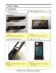
1
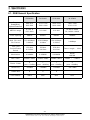
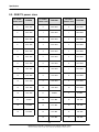
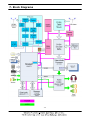
GSM TELEPHONE
SGH-P940
GSM TELEPHONE
CONTENTS
1.
Safety Precautions
2.
Specification
3.
Product Function
4.
Array course control
5.
Exploded View/Disassembly
and Assembly Instructions
6.
MAIN Electrical Parts List
7.
Block Diagrams
8.
PCB Diagrams
9.
Flow Chart of Troubleshooting
10.
Reference data
CONTENTS
1. Safety Precautions
1-1. Repair Precaution......................................................................................................1-1
1-2. ESD(Electrostatically Sensitive Devices) Precaution...............................................1-2
2. Specification
2-1. GSM General Specification.......................................................................................2-1
2-2. GSM Tx Power Class...............................................................................................2-2
3. Product Function
4. Array course control
4-1. Software Adjustments................................................................................................4-1
4-2. Software Downloading...............................................................................................4-2
5. Exploded View/Disassembly & Assembly Instructions
5-1. Cellular phone Exploded View ................................................................................5-1
5-2. Cellular phone Parts list............................................................................................5-2
5-3. Disassembly & Assembly Instructions......................................................................5-4
6. MAIN Electrical Parts List
7. Block Diagrams
8. PCB Diagrams
CONTENTS
9. Flow Chart of Troubleshooting
9-1. Power ON..................................................................................................................9-1
9-2. Initial...........................................................................................................................9-4
9-3. Sim Part.....................................................................................................................9-8
9-4. Speaker Part(Melody)..............................................................................................9-11
9-5. Microphone Part.......................................................................................................9-14
9-6. Key Data Input........................................................................................................9-16
9-7. Receiver Part...........................................................................................................9-17
9-8. Back Light (for Color Main LCD)...........................................................................9-19
9-9. Key Back Light........................................................................................................9-22
9-10. Camera Part...........................................................................................................9-24
9-11. GSM Receiver........................................................................................................9-27
9-12. GSM Transmitter....................................................................................................9-29
9-13. DCS Receiver........................................................................................................9-32
9-14. DCS Transmitter....................................................................................................9-34
9-15. PCS Receiver.........................................................................................................9-37
9-16. PCS Transmitter.....................................................................................................9-39
9-17. WCDMA Receiver..................................................................................................9-42
9-18. WCDMA Transmitter..............................................................................................9-44
9-19. DVB-H.....................................................................................................................9-46
10. Reference data
1. Safety Precautions
1-1. Repair Precaution
― Repair in Shield Box, during detailed tuning.
Take specially care of tuning or test, because specipicty of cellular phone is sensitive for
surrounding interference(RF noise).
― Be careful to use a kind of magnetic object or tool, because performance of parts is damaged by
the influence of magnetic force.
― Surely use a standard screwdriver when you disassemble this product, otherwise screw will be
worn away.
― Use a thicken twisted wire when you measure level.
A thicken twisted wire has low resistance, therefore error of measurement is few.
― Repair after separate Test Pack and Set because for short danger (for example an
overcurrent and furious flames of parts etc) when you repair board in condition of connecting Test
Pack and tuning on.
― Take specially care of soldering, because Land of PCB is small and weak in heat.
― Surely tune on/off while using AC power plug, because a repair of battery charger is dangerous
when tuning ON/OFF PBA and Connector after disassembling charger.
― Don't use as you pleases after change other material than replacement registered on SEC System.
Otherwise engineer in charge isn't charged with problem that you don't keep this rules.
1-1
SAMSUNG Proprietary-Contents may change without notice
This Document can not be used without Samsung's authorization
Safety Precautions
1-2. ESD(Electrostatically Sensitive Devices) Precaution
Several semiconductor may be damaged easily by static electricity. Such parts are called by ESD
(Electrostatically Sensitive Devices), for example IC,BGA chip etc. Read Precaution below.
You can prevent from ESD damage by static electricity.
― Remove static electricity remained your body before you touch semiconductor or parts with
semiconductor. There are ways that you touch an earthed place or wear static electricity prevention
string on wrist.
― Use earthed soldering steel when you connect or disconnect ESD.
― Use soldering removing tool to break static electricity. , otherwise ESD will be damaged by static
electricity.
― Don't unpack until you set up ESD on product. Because most of ESD are packed by box and
aluminum plate to have conductive power,they are prevented from static electricity.
― You must maintain electric contact between ESD and place due to be set up until ESD is
connected completely to the proper place or a circuit board.
1-2
SAMSUNG Proprietary-Contents may change without notice
This Document can not be used without Samsung's authorization
2. Specification
2-1. GSM General Specification
EG SM9 00
DCS1800
PCS1900
W-CDMA
Fr eq.
Band[MHz]
Uplin k/Down link
8 90~915
9 35~960
17 10~178 5
18 05~188 0
18 50~191 0
19 30~199 0
192 0~1980
211 0~2170
ARF CN ra nge
0~ 124 &
97 5~1023
5 12~885
5 12~810
UL:96 12~988 8
DL:105 62~108 38
T x/Rx spacing
45MHz
95MHz
80MHz
1 90MHz
Mo d. Bit r ate/
Bit Period
270 .833kb ps
3 .692u s
270 .833kb ps
3 .692u s
270 .833kb ps
3 .692u s
3.8 4Mcps
Ti me Slo t
Pe rio d/Fr am e
Per iod
5 76.9u s
4. 615ms
5 76.9u s
4. 615ms
5 76.9u s
4. 615ms
Fr ame len gth : 10ms
Modula tion
0 .3G M SK
0 .3G MSK
0 .3G M SK
Q PS K
HQPSK
MS Power
33d Bm~5dBm
30d Bm~0dBm
30d Bm~0dBm
24 dBm ~ - 50dBm
Powe r Class
4
(max +33dBm)
1
(max +30dBm)
1
(max +30dBm)
3
(max + 24dBm)
Se nsitivity
-10 2dBm
-10 0dBm
-10 0dBm
-1 06.7d Bm
TDMA Mu x
8
8
8
Cell Radiu s
35Km
2Km
2Km
2-1
SAMSUNG Proprietary-Contents may change without notice
This Document can not be used without Samsung's authorization
2Km
Specification
2-2. GSM TX power class
TX Power
control level
GSM900
TX Power
DCS1800
control level
TX Power
control level
PCS1800
5
33±2 dBm
0
30±3 dBm
0
30±3 dBm
6
31±2 dBm
1
28±3 dBm
1
28±3 dBm
7
29±2 dBm
2
26±3 dBm
2
26±3 dBm
8
27±2 dBm
3
24±3 dBm
3
24±3 dBm
9
25±2 dBm
4
22±3 dBm
4
22±3 dBm
10
23±2 dBm
5
20±3 dBm
5
20±3 dBm
11
21±2 dBm
6
18±3 dBm
6
18±3 dBm
12
19±2 dBm
7
16±3 dBm
7
16±3 dBm
13
17±2 dBm
8
14±3 dBm
8
14±3 dBm
14
15±2 dBm
9
12±4 dBm
9
12±4 dBm
15
13±2 dBm
10
10±4 dBm
10
10±4 dBm
16
11±3 dBm
11
8±4dBm
11
8±4dBm
17
9±3dBm
12
6±4 dBm
12
6±4 dBm
18
7±3 dBm
13
4±4 dBm
13
4±4 dBm
19
5±3 dBm
14
2±5 dBm
14
2±5 dBm
15
0±5 dBm
15
0±5 dBm
2-2
SAMSUNG Proprietary-Contents may change without notice
This Document can not be used without Samsung's authorization
3. Product Function
Main Function
― 260K Color QVGA Screen (176×320 / 2.15"")
― 6.5K OLED sub Screen (80*64/1.09")
― YAMAHA 64 poly
― Multimedia Message Service (MMS)
― E-mail
― Voice recorder
― Java / WAP2.0
― Quad-band(900/1800/1900/2100MHz)
― Bluetooth (Ver1.2)
― DVB-H
― 2MEGA CAMERA
3-1
SAMSUNG Proprietary-Contents may change without notice
This Document can not be used without Samsung's authorization
Product Function
3-2
SAMSUNG Proprietary-Contents may change without notice
This Document can not be used without Samsung's authorization
4. Array course control
4-1. Software Adjustments
1.
2.
3.
4.
5.
6.
1
2
3
4
5
6
JIG: Download, Trace, Calibration, etc
RF test cable: RF test
Test cable: JIG to phone
TA (Travel Adaptor)
Data Link Cable : USB cable
Serial cable: PC to JIG
4-1
SAMSUNG Proprietary-Contents may change without notice
This Document can not be used without Samsung's authorization
Array course control
4-2. Software Downloading
4-2-1. Downloading Binary Files
• Four binary files for downloading SGH-P940.
– amss.bin : Modem binary for communication function
& Mocha binary for user interface and various application
– Rsrc_P940_Vodafone_Vanilla_Italy: Files need for each application
– Rsrc2_P940(Low).rc2 : Power on/off animation
– FactoryFS_P940_Vodafone_Vanilla_Italy.ffs : Default file system to be put into in
initial production
4-2-2. Pre-requsite for Downloading
• Downloader Program(FastMultiLoader V3.3.exe)
• SGH-P940 Mobile Phone
• USB Data Link Cable
• Binary files
4-2
SAMSUNG Proprietary-Contents may change without notice
This Document can not be used without Samsung's authorization
Array course control
4-2-3. S/W Downloader Program
1. Boot the P940 by pressing ‘Power ON key’ + ‘Number 9 key’ at the same timeIf you do properly, you can see the following message on sub LCD “SGH-P940
DOWNLOAD”
2. Load the binary download program by executing the “FastMultiLoader V3.3.exe”. And
then Check the 6275/6280
4-3
SAMSUNG Proprietary-Contents may change without notice
This Document can not be used without Samsung's authorization
Array course control
3. Select the check box what you want to download.
4. Select the binary file what you want to download
4-4
SAMSUNG Proprietary-Contents may change without notice
This Document can not be used without Samsung's authorization
Array course control
5. Now press the button ‘DownLoad’.
6. When downloading is complete, UE reboot automatically.
- If there is difference in FactoryFs.bin, UE will format file system
automatically.
4-5
SAMSUNG Proprietary-Contents may change without notice
This Document can not be used without Samsung's authorization
Array course control
4-6
SAMSUNG Proprietary-Contents may change without notice
This Document can not be used without Samsung's authorization
5. Exploded View/Disassembly&Assembly Instructions
5-1. Cellular phone Exploded View
QCA01
QKP01
QFU02
QCH01
QME01
QVK02
QMI01
QLC02
QFL02
QFR01
QCR49
QHI01
QMI03
QMP01
QRB01
QFU01
QSH01
QCB01
QMP02
QAN02
QBR04
QCR32
QAN05
QAN01
QMO01
QSP01
QVK01
QCA02
QCR58
QLC01
QSP02
QRE01
QAN04
QIF01
QCK01
QFL01
QRF01
QCR06
QVO01
QCR06
QSC13
QBA01
QCR06
QMW01
QBA00
5-1
SAMSUNG Proprietary-Contents may change without notice
This Document can not be used without Samsung's authorization
Exploded View/Disassembly&Assembly Instructions
5-2. Cellular phone Parts list
Design LOC
QAN01
QAN02
QAN04
QAN05
QBA00
QBA01
QBR04
QCA01
QCA02
QCB01
QCH01
QCK01
QCR06
QCR06
QCR06
QCR32
QCR49
QCR58
QFL01
QFL02
QFR01
QFU01
QFU02
QHI01
QKP01
QLC01
QLC02
QMI03
QMO01
QMP01
QMP02
QMW01
QRB01
QRF01
QSC13
QSH01
QSP01
QSP02
QVK01
QVK02
QVO01
QME01
QRE01
QMI01
QIF01
Description
SEC Code
ANTENNA
INTENNA-SGH P940
FPCB ANTENNA CHIP-SGH P940
ASSY RUBBER-ANT CONTACT
ASSY CASE-BATT
INNER BATTERY PACK-880MAH , BL
ASSY RUBBER-BT
UNIT-CAMERA
UNIT-CAM KEY
COAXIAL CABLE-SGHP940
ASSY HINGE-CAMERA
PMO-CAM KEY
SCREW-MACHINE
SCREW-MACHINE
SCREW-MACHINE
SCREW-MACHINE
SCREW-MACHINE
SCREW-MACHINE
ASSY CASE-FOLDER LOWER
NDC-CASE ARM LOWER V2
ASSY CASE-FRONT
ASSY CASE-FOLDER UPPER
ASSY CASE-ARM UPPER
ASSY-HINGE-SWING HINGE
ASSY KEYPAD-(EU/BLK)
LCD-SGH P940 MODULE
LCD-SUB+FPCB
RMO-RUBBER MIC HOLDER V2
MOTOR DC-SGHT209
PBA MAIN-SGH-P940
PBA-SUB SGH P940
ASSY COVER-WINDOW MAIN
PMO-RING BOARD
MPR-TAPE CAP RF
RMO-RUBBER SCREW CAP REAR
ICT-SHIELD COVER
SPEAKER
SPEAKER
UNIT-VOLUME KEY
UNIT-TOUCH KEY
PMO-VOL KEY
UNIT-KEY FPCB
AS-MIC SVC
ASSY CASE-REAR
PMO-COVER TF
GH42-01008A
GH42-01009A
GH42-01074A
GH98-02820A
GH98-03001A
GH43-02666A
GH98-03568A
GH59-03742A
GH59-03077A
GH39-00687A
GH98-01541A
GH72-36399A
6001-001155
6001-001155
6001-001155
6001-001700
6001-001823
6001-001870
GH98-02815A
GH71-06136A
GH98-02814A
GH98-02817A
GH98-02816A
GH98-01141A
GH98-02819A
GH07-01029A
GH07-01005A
GH73-08833A
GH31-00225A
GH92-03106A
GH92-03118A
GH98-02818A
GH72-35386A
GH74-27676A
GH73-08458A
GH70-01894A
3001-001968
3001-001976
GH59-03076A
GH59-03093A
GH72-28866A
GH59-03704A
GH81-05445A
GH98-02999A
GH72-34693A
5-2
SAMSUNG Proprietary-Contents may change without notice
This Document can not be used without Samsung's authorization
Exploded View/Disassembly&Assembly Instructions
Description
SEC Code
BAG PE
CBF INTERFACE-DATA LINK CABLE
ADAPTOR-SGHE690,BLK,EU,A_TYPE
S/W CD-SGHP940 PC LINK CD
UNIT-EARPHONE,20P,B-TYPE
LABEL(P)-IMEI
LABEL(P)-WATER SOAK
LABEL(R)-MAIN(EU)
MANUAL USERS-OMN ITALIAN
BOX-UNIT(EU)
CUSHION-CASE(EU)
NDC-ANT BUSHING
NDC-ANT E RING
NPR-ANT NUT
PMO-DUMMY CARD
PMO-ANT TUBE
MPR-SPK LEADING TAPE
MPR-BOHO VINYL FOLDER
MPR-TAPE MAIN WINDOW
MPR-TAPE FRONT HINGE
MPR-TAPE SCREW CAP FOLDER
MPR-VINYL BOHO ARM
MPR-INSU TAPE FRONT
MPR-GASK TAPE
MPR-GASK TAPE
MPR-GASK TAPE
MPR-GASK TAPE
MPR-TAPE
MPR-TAPE SCREW CAP ARM
MPR-VINYL BOHO TF COVER
MPR-TAPE
MPR-INSU TAPE
MPR-SPONGE
MPR-INSU TAPE
MPR-INSU TAPE
MPR-INSU TAPE
MPR-INSU TAPE
MPR-INSU TAPE
MPR-INSU TAPE
MPR-INSU TAPE
MPR-INSU TAPE
AS-LCD FPCB
AS-SUB LCD SVC
6902-000634
GH39-00444A
GH44-01361A
GH46-00347A
GH59-03883A
GH68-01335D
GH68-02026A
GH68-13074A
GH68-13082A
GH69-04705A
GH69-04706A
GH71-07141A
GH71-07142A
GH71-07144A
GH72-36453A
GH72-36454A
GH74-12322A
GH74-18217A
GH74-24330A
GH74-24337A
GH74-24355A
GH74-26177B
GH74-27674B
GH74-28820A
GH74-29119A
GH74-29120A
GH74-29121A
GH74-29123A
GH74-29416A
GH74-29559A
GH74-29560A
GH74-29717A
GH74-29719A
GH74-29733A
GH74-29734A
GH74-29762A
GH74-29763A
GH74-29764A
GH74-29765A
GH74-29766A
GH74-29767A
GH81-05945A
GH81-06086A
5-3
SAMSUNG Proprietary-Contents may change without notice
This Document can not be used without Samsung's authorization
Exploded View/Disassembly&Assembly Instructions
5-3. Disassembly&Assembly Instructions
1-1. FRONT ASS'Y & REAR DISASSEMBLY
1
2
Remove SCREW CAP 4 POINT
Remove SCREW 6 POINT
RF SHEET
REAR SCREW CAP
(2POINT)
REAR SCREW
CONNECTION POINT
(6POINT)
1) When remove REAR SCREW CAP and R/F SHEET,
When disjoint SCREW, take care lest scratch
1) When use electric motion driver, take care do
not give damage to REAR.
should occur on ejection.
3
Disassemble the Folder Ass'y and
Rear from the bottom of side
③
4
Disassemble giving flow to right and left.
③
UPPER LOCKER
②
MIDDLE LOCKER
LOWER LOCKER
②
③
②
①
①
1) After Disassemble priority REAR lower column
(①), side (②) and REAR Disjoint top portion (③)
sequentially.
1) When disjoint, Take care LOCKING wealth
damage and scratch attention.
2) When disjoint REAR top portion (③), do not inflict
force and disassemble giving flow to right and
left..
5-4
SAMSUNG Proprietary-Contents may change without notice
This Document can not be used without Samsung's authorization
Exploded View/Disassembly&Assembly Instructions
5
6
Separate MAIN PBA & SUB PBA CONN'.
Disjoint FPCBs
KEYPAD FPCB
MAIN / SUB PBA
CAMERA FPCB
CONN'
LCD FPCB
INTENNA
CONN'
1) When disjoint CONN', pays attention to PIN
damage, and avoids for PBA piece part that
1) Disjoint KEYPAD FPCB, CAMERA FPCB,
LCD FPCB, INTENNA CONN'.
effect goes.
7
When is detached, emancipate PBA.
8
Remove Intenna.
GUIDE
GROOVE
1) When disjoint CONN', pays attention to PIN
damage, and avoids for PBA piece part that
effect goes.
1) Disjoint Coaxial CABLE at left side guide groove.
2) Disjoint Intenna from right side on FRONT lower
column.
3) Disjoint COAXIAL CABLE at Intenna
5-5
SAMSUNG Proprietary-Contents may change without notice
This Document can not be used without Samsung's authorization
Exploded View/Disassembly&Assembly Instructions
9
10
Remove TAPE.
DUST PREVENTION TAPE
INTENNA
INSULATION TAPE
1) Remove dust prevention TAPE and insulation
TAPE.
1) When Intenna disjoints, Do not inflict force to do
damage does not go to LOCKER.
2) When disjoint COAXIAL CABLE, Avoid expiring
or deform CABLE and CABLE CONN'.
11
Disjoint FOLDER ASSY'.
12
LEFT
HINGE PRESS POINT
RIGHT
1) Disjoint right side and after extract left FPCB,
Separate FOLDER ASS' Y and FRONT
1) Take care so that do not inflict force perforce.
2) When disjoint FPCB, take care so that FPCB may
not tear.
5-6
SAMSUNG Proprietary-Contents may change without notice
This Document can not be used without Samsung's authorization
Exploded View/Disassembly&Assembly Instructions
1-2. FOLDER DISASSEMBLY
1
2
Remove SCREW CAP & SCREW 4 POINT.
Disjoint LOCKER.
①
②
③
SCREW CAP
& FOLDER SCREW
(4POINT)
④
⑤
1) After disjoint first side LOCKER ( ②, ③, ④),
1) When disjoint SCREW, SCREW CAP, scratch
attention
Disjoint LOCKER (①, ⑤).
2) When disjoint, take care so that damage may not
go to LOCKER.
3
4
Separate FOLDER LOWER / UPPER.
Remove FOLDER UPPER SCREW 4 POINT.
SCREW CONNECTION
4POINT
LCD FPCB
1) When disjoint FPCB, take care lest FPCB should
tear.
1) After FOLDER UPPER SCREW 4 point, Extracting
SUB LCD ASS' Y FPCB through Hole.
2) Separate UPPER and ARM.
5-7
SAMSUNG Proprietary-Contents may change without notice
This Document can not be used without Samsung's authorization
Exploded View/Disassembly&Assembly Instructions
5
6
Separate UPPER and ARM.
1) When remove insulation TAPE, avoid influencing
1) Take care so that FPCB may not tear or fold.
7
for piece part..
8
Separate each parts.
LCD CONN'
Remove INSULATION TAPE.
Remove WINDOW in LOWER.
SPK(R)
DUAL
SPONGE
MOTOR
SAPARATE
SPK(L)
WINDOW
1) Separate CAMERA KEY, VOLUME KEY, SPK,
1) When remove, Scratch Attention.
MOTOR, LCD CONN in FOLDER LOWER.
2) When separate each parts, Avoid
- When remove dust, use alcohol and swab.
parts
interference and FPCB/WIRE tearing or get taken.
5-8
SAMSUNG Proprietary-Contents may change without notice
This Document can not be used without Samsung's authorization
Exploded View/Disassembly&Assembly Instructions
1-3. ARM DISASSEMBLY
1
Remove ARM SCREW SHEET.
2
Disjoint SCREW.
DISJOINT SCREW (6 POINT)
ARM SCREW SHEET
1) REMOVE ARM SCREW SHEET.
3
1) When disjoint SCREW, Scratch Attention.
4
Extract SUB LCD FPCB.
Remove TAPE and Separate ARM
UPPER / LOWER.
1) When extract SUB LCD FPCB, Take care so that
FPCB may not tear.
1) Remove INSULATION TAPE of detached ARM
UPPER's lower column.
2) After disjoint TOUCH KEY FPCB ARM, Separate
perfectly UPPER / LOWER.
3) Take care so that TOUCH KEY FPCB
may not tear.
5-9
SAMSUNG Proprietary-Contents may change without notice
This Document can not be used without Samsung's authorization
Exploded View/Disassembly&Assembly Instructions
5
Separate ARM UPPER's TOUCH
6
KEY FPCB
Disassembly SUB LCD MODULE.
TOUCH KEY FPCB
1) Take care so that TOUCH KEY FPCB
may not tear.
7
Disjoint HINGE DUMMY.
1) Take care so that FPCB may not tear.
8
Extract HINGE.
HINGE DUMMY
HINGE
1) When disjoint HINGE DUMMY, take care so
that
1) Extract HINGE and Cancel CAMERA fixing state.
CAMERA FPCB may not tear.
5-10
SAMSUNG Proprietary-Contents may change without notice
This Document can not be used without Samsung's authorization
Exploded View/Disassembly&Assembly Instructions
9
Separate CAMERA.
FPCB CRACK OCCURRENCE
1) When separate CAMERA, Take care so that
CAMERA FPCB may not tear.
1-4. LCD DISASSEMBLY
1
Separate ARM UPPER's TOUCH KEY FPCB.
2
Disjoint SUB LCD MODULE.
MOTOR
SPK
BONDING PART
VOLUME KEY
CAMERA KEY
SPK
1) Remove SPK & MOTOR's bonding and disjoint
SOLDERING segment.
2) When remove SOLDERING, Do not to effect goes
for neighborhood piece part.
1) Remove and Disjoint SOLDERING part of
VOLUME KEY, CAM KEY.
2) Take care lest FPCB should tear.
5-11
SAMSUNG Proprietary-Contents may change without notice
This Document can not be used without Samsung's authorization
Exploded View/Disassembly&Assembly Instructions
2-1. LCD ASSEMBLY
1
2
KEY FPCB does SOLDERING.
Parts do SOLDERING.
+
+
-
SPEAKER(L) MANUAL
SOLDERING part
MOTOR MANUAL
SOLDERING part
+
1) When SOLDERING, avoid influencing for
neighborhood piece part.
2) First, Do MANUAL SOLDERING to LAND to do
MANUAL SOLDERING.
3
-
1) Do MANUAL SOLDERING Where red WIRE is
FPCB's (+) la and is registered.
(Observe in polarity)
2) When SOLDERING, avoid influencing for
neighborhood piece part.
Do bonding.
+
-
SPEAKER, MOTOR
BONDING
1) Work bonding in SPEAKER WIRE's neck region.
2) Work as do not become excess bonding.
3) Glue works as do not escape GUIDE LINE.
5-12
SAMSUNG Proprietary-Contents may change without notice
This Document can not be used without Samsung's authorization
Exploded View/Disassembly&Assembly Instructions
2-2. ARM ASSEMBLY
1
Insert CAMERA.
2
Remove SCREW 6 POINTs.
HINGE
Press hinge
FPCB CRACK
OCCURENCE
1) Make CAMERA insertion space after press hinge
to outer block.
2) When insert CAMERA, Pull FPCB downward so
that FPCB may not get torn.
3) Take care lest should tear to FPCB and
contracts.
3
Confirm HINGE DUMMY.
1) Does CAMERA insertion and uses hinge, Fix
CAMERA.
4
Confirm CAMERA insertion.
HINGE DUMMY
Agreement
1) Contracts HINGE DUMMY and
Insert perfectly
1) When was inserted, fix HINGE DUMMY and
CAMERA When turn downward, do not return
CAMERA.
2) Observe in FPCB and hinge direction after
CAMERA insertion.
downward at relevant position.
2) When connect hinge DUMMY, Take care lest
should tear to FPCB.
5-13
SAMSUNG Proprietary-Contents may change without notice
This Document can not be used without Samsung's authorization
Exploded View/Disassembly&Assembly Instructions
SUB LCD to ARM LOWER
5
6
safe arrival.
Connect TOUCH KEY FPCB.
SUB WINDOW
Protection vinyl
ATTACH
INSULATION TAPE
SUB WINDOW ATTACH TAPE
FIXING
PROJECTION
1) Attach TOUCH KEY FPCB to ARM UPPER CONN'
1) Attach TOUCH KEY FPCB to ARM UPPER.
2) When Attach TOUCH KEY FPCB, Attach by
projection standard for fixing.
2) Remove SUB WINDOW protection vinyl & SUB
WINDOW attach tape.
3) Do to insert perfectly guide line.
4) Take care so that insulation TAPE may not
get loose.
7
When is detached, separate PBA.
8
Remove Intena.
②
①
SUB LCD FPCB(FRONT)
CAMERA FPCB(BACK)
1) After insert SUB LCD FPCB to HINGE DUMMY
(①), Connect ARM UPPER and ARM LOWER
1) Take care so that FPCB may not tear.
2) SUB LCD FPCB is front, CAMERA FPCB is
(FPCB direction attention)
backward.
5-14
SAMSUNG Proprietary-Contents may change without notice
This Document can not be used without Samsung's authorization
Exploded View/Disassembly&Assembly Instructions
Insert SUB LCD FPCB in ROTATE
9
10
Connect SCREW 6 POINTs.
HINGE
DISJOINT SCREW
(6 POINT)
1) ROTATE HINGE's triangle symbol is combined
to CAMERA. (When direction is not right, do
1) When contract SCREW, Take care so that scratch
does not occur.
not become safe arrival perfectly)
2) Take care lest FPCB should tear.
11
Attach ARM SCREW SHEET.
ARM SCREW SHEET
1) Attach ARM SCREW SHEET.
5-15
SAMSUNG Proprietary-Contents may change without notice
This Document can not be used without Samsung's authorization
Exploded View/Disassembly&Assembly Instructions
2-3. FRONT ASSEMBLY
1
Attach TAPEs.
2
Attach black insulation TAPE.
DUST PREVENTION TAPE
INSULATION
TAPE
1) Central TAPE ( INSULATION TAPE →
1) Sets well in holdfast directrix and attaches
CHALLENGE TAPE → INSULATION TAPE )
INSULATION TAPE.
5-16
SAMSUNG Proprietary-Contents may change without notice
This Document can not be used without Samsung's authorization
Exploded View/Disassembly&Assembly Instructions
2-4. FOLDER ASSEMBLY
1
Inserts parts to case and attaches
Attach WINDOW.
2
TAPE.
DUAL SPONGE
WINDOW
1) Attach WINDOW.
2) When handle to WINDOW, observe in dust
management. ( When remove dust, use alcohol
and swab. )
3
Assemble UPPER and ARM.
1) Insert SPK(L), SPK(R), MOTOR and LCD CONN'.
2) Attach INSULATION TAPE.
3) Take care so that WIRE may gets snarl
and does not drop.
4
CONNECT FOLDER UPPER SCREW
4 POINT
CONNECT SCREW
4POINT
1) Insert SUB LCD ASS' Y's FPCB through
FOLDER UPPER HOLE.
2) Do ROTATE HINGE so that arrive safe to
FOLDER UPPER.
3) When insert FPCB, take care so that FPCB may
not tear.
1) When contract SCREW, Take care so that scratch
does not occur.
5-17
SAMSUNG Proprietary-Contents may change without notice
This Document can not be used without Samsung's authorization
Exploded View/Disassembly&Assembly Instructions
5
Assemble UPPER and ARM.
6
Remove insulation TAPE.
①
②
③
④
⑤
LCD FPCB
VOLUME KEY
CAMERA KEY
1) Assemble in LOCKER's order. ( ① → ② )
1) Assemble LCD FPCB to FOLDER UPPER.
2) Take care so that FPCB may not tear or fold.
2) Assemble VOLUME KEY & CAMERA KEY.
3) Assemble in LOCKER's order. ( ③ → ④ → ⑤ )
4) Observe in VOLUME KEY & CAMERA KEY's
inclination.
7
CONNECT FOLDER SCREW
SCREW CAP
& FOLDER SCREW
(4POINT)
1) Attach FOLDER SCREW CAP (4POINT).
2) When contract SCREW, observe shooting out
scratch.
3) SCREW CAP fix as once more as possible
press.
5-18
SAMSUNG Proprietary-Contents may change without notice
This Document can not be used without Samsung's authorization
Exploded View/Disassembly&Assembly Instructions
2-5. FRONT ASS'Y & REAR ASSEMBLY
2
1
Assemble folder.
①
②
1) Make CAMERA lens turn front side.
3
Extract SUB LCD FPCB.
1) Rush LCD FPCB & CAMERA FPCB to FRONT's
groove.
2) Insert to FRONT from HINGE DUMMY (①).
3) Presses and assembles projected part (②).
4) Opens FOLDER and repeats close of 2 times.
4
Assemble INTENNA to REAR.
INTENNA
OBSERVE on HINGE DUMMY direction
1) Take care so that FPCB may not be chewed.
1) Assembles Intena from left side and right side.
2) At left side assembly Confirm whether was
arrived safe to KEY PCB GND.
3) Take care so that COAXIAL CABLE may not
be chewed.
5-19
SAMSUNG Proprietary-Contents may change without notice
This Document can not be used without Samsung's authorization
Exploded View/Disassembly&Assembly Instructions
5
ASSEMBLE FPCB & INTENNA CONN'
KEYPAD FPCB
6
CAMERA FPCB
ASSEMBLE MAIN / SUB PBA
MAIN / SUB PBA CONN'
LCD FPCB
INTENNA CONN'
1) Insert MAIN PBA to SCREW BOSS's(4ea) HOLE.
2) Assemble INTENNA WIRE, LCD FPCB.
3) Assemble CAMERA FPCB, KEYPAD FPCB.
1) When insert PBA, insert vertically.
8
7
ASSEMBLE
UPPER LOCKER
CONNECT REAR SCREW 6 POINT
REAR.
MIDDLE LOCKER
LOWER LOCKER
CONNECT REAR
SCREW POINT
1) Assemble Left LOCKER, Right LOCKER and
Lower LOCKER.
2) Observe for LOCKING wealth damage.
3) Take care so that RF WIRE may not be chewed
at LOCKER assembly.
1) When contract SCREW, Take care so that scratch
does not occur.
5-20
SAMSUNG Proprietary-Contents may change without notice
This Document can not be used without Samsung's authorization
Exploded View/Disassembly&Assembly Instructions
9
ASSEMBLE
FPCB & INTENNA CONN' .
RF SHEET
REAR SCREW
CAP (2POINT)
1) Insert REAR SCREW CAP to 4 POINTs of picture.
2) Attach R/F SHEET.
5-21
SAMSUNG Proprietary-Contents may change without notice
This Document can not be used without Samsung's authorization
Exploded View/Disassembly&Assembly Instructions
5-22
SAMSUNG Proprietary-Contents may change without notice
This Document can not be used without Samsung's authorization
6. MAIN Electrical Parts List
Design LOC
Description
SEC Code
STATUS
ANT1
BAT900
BTC700
C100
C1000
C1001
C1002
C1003
C1004
C1005
C1006
C1007
C1008
C1009
C101
C1010
C1011
C1012
C1013
C1014
C1017
C1018
C1019
C102
C1020
C1021
C1022
C1023
C1024
C1025
C1026
C1027
C1028
C1029
C103
C1030
C1031
C1032
C1033
C1034
C1035
C1036
C1037
C1038
C1039
C104
C1040
C1041
C1042
C1043
C1044
C1045
C1046
NPR-ANTENNA CONTACT
BATTERY-LI(2ND)
CONNECTOR-BATTERY
C-CER,CHIP
C-CER,CHIP
C-CER,CHIP
C-CER,CHIP
C-CER,CHIP
C-CER,CHIP
C-CER,CHIP
C-CER,CHIP
C-CER,CHIP
C-CER,CHIP
C-CER,CHIP
C-CER,CHIP
C-CER,CHIP
C-CER,CHIP
C-CER,CHIP
C-CER,CHIP
C-CER,CHIP
C-CER,CHIP
C-CER,CHIP
C-CER,CHIP
C-CER,CHIP
C-CER,CHIP
C-CER,CHIP
C-CER,CHIP
C-CER,CHIP
C-CER,CHIP
C-CER,CHIP
C-CER,CHIP
C-CER,CHIP
C-CER,CHIP
C-CER,CHIP
C-CER,CHIP
C-CER,CHIP
C-CER,CHIP
C-CER,CHIP
C-CER,CHIP
C-CER,CHIP
C-CER,CHIP
C-CER,CHIP
C-CER,CHIP
C-CER,CHIP
C-CER,CHIP
C-CER,CHIP
C-CER,CHIP
C-CER,CHIP
C-CER,CHIP
C-CER,CHIP
C-CER,CHIP
C-CER,CHIP
C-CER,CHIP
GH71-06984A
4302-001130
3711-006003
2203-002982
2203-005725
2203-006423
2203-005725
2203-005725
2203-005725
2203-006708
2203-006423
2203-006708
2203-006708
2203-006423
2203-006123
2203-006423
2203-006708
2203-006423
2203-006562
2203-006423
2203-006423
2203-006423
2203-006423
2203-001124
2203-000854
2203-006423
2203-006423
2203-006423
2203-006824
2203-006423
2203-000330
2203-006423
2203-006423
2203-006423
2203-005808
2203-006423
2203-000330
2203-006423
2203-006824
2203-006423
2203-006562
2203-006562
2203-006562
2203-006562
2203-006423
2203-005808
2203-006423
2203-006562
2203-006423
2203-006423
2203-006423
2203-006824
2203-006562
SA
SA
SA
SA
SA
SA
SA
SA
SA
SA
SA
SA
SA
SA
SA
SA
SA
SA
SA
SA
SA
SA
SA
DNA
SA
SA
SA
SA
SA
SA
SA
SA
SA
SA
SA
SA
SA
SA
SA
SA
SA
SA
SA
SA
SA
SA
SA
SA
SA
SA
SA
SA
SA
6-1
SAMSUNG Proprietary-Contents may change without notice
This Document can not be used without Samsung's authorization
Main Electrical Parts List
Design LOC
Description
SEC Code
STATUS
C1047
C1048
C1049
C105
C1050
C1051
C1052
C1053
C106
C108
C109
C110
C111
C112
C113
C114
C115
C116
C117
C119
C120
C121
C122
C123
C124
C125
C126
C127
C128
C129
C130
C131
C132
C133
C134
C135
C136
C137
C138
C139
C140
C141
C142
C143
C144
C145
C146
C147
C148
C149
C150
C151
C152
C-CER,CHIP
C-CER,CHIP
C-CER,CHIP
C-CER,CHIP
C-CER,CHIP
C-CER,CHIP
C-CER,CHIP
C-CER,CHIP
C-CER,CHIP
C-CER,CHIP
C-CER,CHIP
C-CER,CHIP
C-CER,CHIP
C-CER,CHIP
C-CER,CHIP
C-CER,CHIP
C-CER,CHIP
C-CER,CHIP
C-CER,CHIP
C-CER,CHIP
C-CER,CHIP
C-CER,CHIP
C-CER,CHIP
C-CER,CHIP
C-CER,CHIP
C-CER,CHIP
C-CER,CHIP
C-CER,CHIP
C-CER,CHIP
C-CER,CHIP
C-CER,CHIP
C-CER,CHIP
C-CER,CHIP
C-CER,CHIP
C-CER,CHIP
C-CER,CHIP
C-CER,CHIP
C-CER,CHIP
C-CER,CHIP
C-CER,CHIP
C-CER,CHIP
C-CER,CHIP
C-CER,CHIP
C-CER,CHIP
C-CER,CHIP
C-CER,CHIP
C-CER,CHIP
C-CER,CHIP
C-CER,CHIP
C-CER,CHIP
C-CER,CHIP
C-CER,CHIP
C-CER,CHIP
2203-006562
2203-006824
2203-006708
2203-005806
2203-001432
2203-006708
2203-006824
2203-000854
2203-005682
2203-006423
2203-005682
2203-005682
2203-006423
2203-005719
2203-005682
2203-006423
2203-006379
2203-005736
2203-005682
2203-006423
2203-005806
2203-005682
2203-005808
2203-005682
2203-006556
2203-005682
2203-005682
2203-006556
2203-005682
2203-005808
2203-005717
2203-006423
2203-005682
2203-005717
2203-000725
2203-000836
2203-005682
2203-006423
2203-006423
2203-005682
2203-000438
2203-005682
2203-005719
2203-000812
2203-006838
2203-000812
2203-005682
2203-006208
2203-006423
2203-005729
2203-000254
2203-005729
2203-005732
SA
SA
SA
SNA
SA
SA
SA
SA
SA
SA
SA
SA
SA
SA
SA
SA
SA
SA
SA
SA
SNA
SA
SA
SA
SA
SA
SA
SA
SA
SA
SA
SA
SA
SA
SA
SA
SA
SA
SA
SA
SA
SA
SA
SA
SA
SA
SA
SA
SA
SA
SA
SA
SA
6-2
SAMSUNG Proprietary-Contents may change without notice
This Document can not be used without Samsung's authorization
Main Electrical Parts List
Design LOC
Description
SEC Code
STATUS
C153
C154
C155
C156
C157
C158
C160
C200
C201
C202
C203
C204
C205
C206
C207
C208
C209
C210
C211
C212
C214
C216
C217
C218
C219
C220
C221
C222
C223
C224
C225
C226
C227
C228
C229
C230
C231
C232
C233
C234
C235
C236
C237
C238
C239
C300
C301
C302
C303
C304
C305
C306
C307
C-CER,CHIP
C-CER,CHIP
C-CER,CHIP
C-CER,CHIP
C-CER,CHIP
C-CER,CHIP
C-CER,CHIP
C-CER,CHIP
C-CER,CHIP
C-CER,CHIP
C-CER,CHIP
C-CER,CHIP
C-CER,CHIP
C-CER,CHIP
C-CER,CHIP
C-CER,CHIP
R-CHIP
C-CER,CHIP
C-CER,CHIP
C-CER,CHIP
R-CHIP
C-CER,CHIP
C-CER,CHIP
C-CER,CHIP
C-CER,CHIP
C-CER,CHIP
C-CER,CHIP
C-CER,CHIP
C-CER,CHIP
C-CER,CHIP
C-CER,CHIP
C-CER,CHIP
C-CER,CHIP
C-CER,CHIP
C-CER,CHIP
C-CER,CHIP
C-CER,CHIP
C-CER,CHIP
C-CER,CHIP
C-CER,CHIP
C-CER,CHIP
C-CER,CHIP
C-CER,CHIP
C-CER,CHIP
C-CER,CHIP
C-CER,CHIP
C-CER,CHIP
C-CER,CHIP
C-CER,CHIP
C-CER,CHIP
C-CER,CHIP
C-CER,CHIP
C-CER,CHIP
2203-000254
2203-002443
2203-000311
2203-001033
2203-000995
2203-006423
2203-001153
2203-005736
2203-006194
2203-005736
2203-005968
2203-006324
2203-006194
2203-000233
2203-000386
2203-000854
2007-000171
2203-005382
2203-000330
2203-002668
2007-000171
2203-000386
2203-006194
2203-005736
2203-005808
2203-006423
2203-005806
2203-006194
2203-005736
2203-005719
2203-006423
2203-006305
2203-006846
2203-005806
2203-000330
2203-006423
2203-006846
2203-005806
2203-005682
2203-006556
2203-005736
2203-006423
2203-006423
2203-006305
2203-006305
2203-006423
2203-006617
2203-006423
2203-005725
2203-005725
2203-006668
2203-006423
2203-006617
SA
SA
SA
SA
SA
SA
SA
SA
SA
SA
SA
SA
SA
SA
SA
SA
SA
SA
SA
SA
SA
SA
SA
SA
SA
SA
SNA
SA
SA
SA
SA
SA
SA
SNA
SA
SA
SA
SNA
SA
SA
SA
SA
SA
SA
SA
SA
SA
SA
SA
SA
SA
SA
SA
6-3
SAMSUNG Proprietary-Contents may change without notice
This Document can not be used without Samsung's authorization
Main Electrical Parts List
Design LOC
Description
SEC Code
STATUS
C308
C309
C310
C311
C312
C313
C314
C315
C316
C317
C318
C319
C320
C321
C322
C323
C324
C325
C326
C327
C328
C329
C330
C331
C332
C333
C334
C335
C336
C337
C338
C339
C340
C341
C342
C343
C344
C345
C346
C347
C348
C349
C350
C351
C352
C353
C354
C355
C356
C357
C358
C359
C360
C-CER,CHIP
C-CER,CHIP
C-CER,CHIP
C-CER,CHIP
C-CER,CHIP
C-CER,CHIP
C-CER,CHIP
C-CER,CHIP
C-CER,CHIP
C-CER,CHIP
C-CER,CHIP
C-CER,CHIP
C-CER,CHIP
C-CER,CHIP
C-CER,CHIP
C-CER,CHIP
C-CER,CHIP
C-CER,CHIP
C-CER,CHIP
C-CER,CHIP
C-CER,CHIP
C-CER,CHIP
C-CER,CHIP
C-CER,CHIP
C-CER,CHIP
C-CER,CHIP
C-CER,CHIP
C-CER,CHIP
C-CER,CHIP
C-CER,CHIP
C-CER,CHIP
C-CER,CHIP
C-CER,CHIP
C-CER,CHIP
C-CER,CHIP
C-CER,CHIP
C-CER,CHIP
C-CER,CHIP
C-CER,CHIP
C-CER,CHIP
C-CER,CHIP
C-CER,CHIP
C-CER,CHIP
C-CER,CHIP
C-CER,CHIP
C-CER,CHIP
C-CER,CHIP
C-CER,CHIP
C-CER,CHIP
C-CER,CHIP
C-CER,CHIP
C-CER,CHIP
C-CER,CHIP
2203-006423
2203-006194
2203-006462
2203-006423
2203-006423
2203-006423
2203-006562
2203-006562
2203-006708
2203-006423
2203-006423
2203-006708
2203-005482
2203-006194
2203-006194
2203-000233
2203-005682
2203-006825
2203-005719
2203-005806
2203-005806
2203-006194
2203-006194
2203-006194
2203-006194
2203-006194
2203-006194
2203-006423
2203-005719
2203-005806
2203-005806
2203-006194
2203-006194
2203-005806
2203-005806
2203-006194
2203-006423
2203-005719
2203-006194
2203-006194
2203-006423
2203-006423
2203-006423
2203-006423
2203-006194
2203-006194
2203-006194
2203-006825
2203-006423
2203-006423
2203-006423
2203-006423
2203-006423
SA
SA
SA
SA
SA
SA
SA
SA
SA
SA
SA
SA
SA
SA
SA
SA
SA
SA
SA
SNA
SNA
SA
SA
SA
SA
SA
SA
SA
SA
SNA
SNA
SA
SA
SNA
SNA
SA
SA
SA
SA
SA
SA
SA
SA
SA
SA
SA
SA
SA
SA
SA
SA
SA
SA
6-4
SAMSUNG Proprietary-Contents may change without notice
This Document can not be used without Samsung's authorization
Main Electrical Parts List
Design LOC
Description
SEC Code
STATUS
C361
C400
C401
C402
C403
C404
C405
C406
C407
C408
C409
C410
C411
C412
C413
C414
C415
C416
C417
C418
C419
C420
C421
C422
C423
C424
C425
C426
C427
C428
C429
C430
C431
C432
C433
C434
C435
C436
C437
C438
C439
C440
C441
C442
C443
C444
C445
C446
C447
C448
C449
C450
C451
C-CER,CHIP
C-CER,CHIP
C-CER,CHIP
C-CER,CHIP
C-CER,CHIP
C-CER,CHIP
C-CER,CHIP
C-CER,CHIP
C-CER,CHIP
C-CER,CHIP
C-CER,CHIP
C-CER,CHIP
C-CER,CHIP
C-CER,CHIP
C-CER,CHIP
C-CER,CHIP
C-CER,CHIP
C-CER,CHIP
C-CER,CHIP
C-CER,CHIP
C-CER,CHIP
C-CER,CHIP
C-CER,CHIP
C-CER,CHIP
C-CER,CHIP
C-CER,CHIP
C-CER,CHIP
C-CER,CHIP
C-CER,CHIP
C-CER,CHIP
C-CER,CHIP
C-CER,CHIP
C-CER,CHIP
C-CER,CHIP
C-CER,CHIP
C-CER,CHIP
C-CER,CHIP
C-CER,CHIP
C-CER,CHIP
C-CER,CHIP
C-CER,CHIP
C-CER,CHIP
C-CER,CHIP
C-CER,CHIP
C-CER,CHIP
C-CER,CHIP
C-CER,CHIP
C-CER,CHIP
C-CER,CHIP
C-CER,CHIP
C-CER,CHIP
C-CER,CHIP
C-CER,CHIP
2203-006423
2203-005719
2203-006423
2203-006324
2203-006348
2203-006208
2203-006562
2203-005682
2203-006423
2203-005731
2203-005736
2203-005731
2203-006423
2203-006562
2203-006838
2203-006208
2203-006208
2203-006208
2203-006838
2203-006305
2203-006562
2203-006208
2203-006838
2203-006305
2203-006838
2203-006838
2203-006305
2203-006562
2203-006305
2203-006562
2203-006305
2203-005806
2203-005806
2203-005682
2203-006423
2203-006423
2203-006423
2203-006423
2203-006838
2203-006838
2203-006208
2203-005806
2203-005806
2203-005806
2203-006423
2203-006423
2203-006048
2203-006048
2203-006562
2203-006562
2203-006562
2203-006681
2203-006562
SA
SA
SA
SA
SA
SA
SA
SA
SA
SA
SA
SA
SA
SA
SA
SA
SA
SA
SA
SA
SA
SA
SA
SA
SA
SA
SA
SA
SA
SA
SA
SNA
SNA
SA
SA
SA
SA
SA
SA
SA
SA
SNA
SNA
SNA
SA
SA
SA
SA
SA
SA
SA
SA
SA
6-5
SAMSUNG Proprietary-Contents may change without notice
This Document can not be used without Samsung's authorization
Main Electrical Parts List
Design LOC
Description
SEC Code
STATUS
C452
C453
C455
C502
C504
C506
C507
C508
C509
C510
C513
C515
C517
C518
C519
C520
C522
C524
C525
C526
C528
C530
C531
C532
C533
C534
C535
C536
C538
C539
C540
C541
C542
C544
C545
C547
C551
C556
C559
C560
C561
C562
C563
C564
C565
C567
C568
C569
C570
C571
C572
C573
C574
C-CER,CHIP
C-CER,CHIP
C-TA,CHIP
C-CER,CHIP
C-CER,CHIP
C-CER,CHIP
C-CER,CHIP
C-CER,CHIP
C-CER,CHIP
C-CER,CHIP
C-CER,CHIP
C-CER,CHIP
C-CER,CHIP
C-CER,CHIP
C-CER,CHIP
C-CER,CHIP
C-CER,CHIP
C-CER,CHIP
C-CER,CHIP
C-CER,CHIP
C-CER,CHIP
C-CER,CHIP
C-CER,CHIP
C-CER,CHIP
C-CER,CHIP
C-CER,CHIP
C-CER,CHIP
C-CER,CHIP
C-CER,CHIP
C-CER,CHIP
C-CER,CHIP
C-CER,CHIP
C-CER,CHIP
C-CER,CHIP
C-CER,CHIP
C-CER,CHIP
C-CER,CHIP
C-CER,CHIP
C-CER,CHIP
C-CER,CHIP
C-CER,CHIP
C-CER,CHIP
C-CER,CHIP
C-CER,CHIP
C-CER,CHIP
C-CER,CHIP
C-CER,CHIP
C-CER,CHIP
C-CER,CHIP
C-CER,CHIP
C-CER,CHIP
C-CER,CHIP
C-CER,CHIP
2203-006562
2203-006562
2404-001225
2203-000812
2203-006562
2203-006423
2203-006423
2203-006708
2203-006423
2203-006423
2203-000386
2203-006562
2203-006648
2203-006562
2203-006562
2203-006562
2203-006648
2203-006423
2203-006556
2203-005057
2203-006423
2203-006423
2203-006556
2203-005057
2203-006648
2203-006648
2203-000654
2203-000654
2203-005344
2203-006668
2203-005736
2203-006562
2203-005344
2203-005383
2203-000812
2203-000386
2203-006648
2203-006648
2203-005682
2203-001259
2203-001259
2203-005682
2203-005682
2203-001259
2203-005383
2203-005383
2203-005683
2203-005683
2203-005683
2203-005682
2203-001259
2203-001259
2203-005682
SA
SA
SA
SA
SA
SA
SA
SA
SA
SA
SA
SA
SA
SA
SA
SA
SA
SA
SA
SA
SA
SA
SA
SA
SA
SA
SA
SA
SA
SA
SA
SA
SA
SA
SA
SA
SA
SA
SA
SA
SA
SA
SA
SA
SA
SA
SA
SA
SA
SA
SA
SA
SA
6-6
SAMSUNG Proprietary-Contents may change without notice
This Document can not be used without Samsung's authorization
Main Electrical Parts List
Design LOC
Description
SEC Code
STATUS
C575
C576
C577
C601
C602
C603
C604
C605
C606
C607
C608
C609
C610
C611
C612
C613
C614
C615
C616
C617
C618
C619
C620
C621
C622
C623
C625
C626
C627
C628
C629
C630
C631
C632
C633
C634
C635
C703
C704
C705
C707
C708
C709
C710
C711
C712
C800
C801
C802
C803
C804
C805
C806
C-CER,CHIP
C-CER,CHIP
C-CER,CHIP
C-CER,CHIP
C-CER,CHIP
C-CER,CHIP
C-CER,CHIP
C-CER,CHIP
C-CER,CHIP
C-CER,CHIP
C-CER,CHIP
C-CER,CHIP
C-CER,CHIP
C-CER,CHIP
C-CER,CHIP
C-CER,CHIP
C-CER,CHIP
C-CER,CHIP
C-CER,CHIP
C-CER,CHIP
C-CER,CHIP
C-CER,CHIP
C-CER,CHIP
C-CER,CHIP
C-CER,CHIP
C-CER,CHIP
C-CER,CHIP
C-CER,CHIP
C-CER,CHIP
C-CER,CHIP
C-CER,CHIP
C-CER,CHIP
C-CER,CHIP
C-CER,CHIP
C-CER,CHIP
C-CER,CHIP
C-CER,CHIP
C-CER,CHIP
C-CER,CHIP
C-CER,CHIP
C-CER,CHIP
C-CER,CHIP
C-CER,CHIP
C-CER,CHIP
C-CER,CHIP
C-CER,CHIP
C-CER,CHIP
C-CER,CHIP
C-CER,CHIP
C-CER,CHIP
C-CER,CHIP
C-CER,CHIP
C-CER,CHIP
2203-005682
2203-001259
2203-006681
2203-006423
2203-006423
2203-006423
2203-006423
2203-006423
2203-006423
2203-006423
2203-006708
2203-006708
2203-006708
2203-005725
2203-000278
2203-006838
2203-006838
2203-006423
2203-006562
2203-006562
2203-006562
2203-006562
2203-000278
2203-000278
2203-006423
2203-006423
2203-006423
2203-006423
2203-006423
2203-006423
2203-006423
2203-006423
2203-006708
2203-006423
2203-006838
2203-006423
2203-000438
2203-005736
2203-005682
2203-006423
2203-002709
2203-006562
2203-006562
2203-006562
2203-000438
2203-006423
2203-006562
2203-006562
2203-006562
2203-005682
2203-005682
2203-006562
2203-005682
SA
SA
SA
SA
SA
SA
SA
SA
SA
SA
SA
SA
SA
SA
SA
SA
SA
SA
SA
SA
SA
SA
SA
SA
SA
SA
SA
SA
SA
SA
SA
SA
SA
SA
SA
SA
SA
SA
SA
SA
SA
SA
SA
SA
SA
SA
SA
SA
SA
SA
SA
SA
SA
6-7
SAMSUNG Proprietary-Contents may change without notice
This Document can not be used without Samsung's authorization
Main Electrical Parts List
Design LOC
Description
SEC Code
STATUS
C807
C808
C809
C810
C811
C812
C813
C814
C815
C816
C901
C902
C903
C905
C906
C908
C909
C910
C911
C912
C913
C914
C915
C916
CD900
D1000
D401
D402
D403
DUF200
F101
F201
F202
F800
F801
F802
F803
F804
F805
F806
HDC300
HDC700
HDC800
HDC801
HDC802
IFC700
L100
L1000
L1001
L1002
L1003
L1004
L1005
C-CER,CHIP
C-CER,CHIP
C-CER,CHIP
C-CER,CHIP
C-CER,CHIP
C-CER,CHIP
C-CER,CHIP
C-CER,CHIP
C-CER,CHIP
C-CER,CHIP
C-CER,CHIP
C-CER,CHIP
C-CER,CHIP
C-CER,CHIP
C-CER,CHIP
C-CER,CHIP
C-CER,CHIP
C-CER,CHIP
C-CER,CHIP
C-CER,CHIP
C-CER,CHIP
C-CER,CHIP
C-CER,CHIP
C-CER,CHIP
CONNECTOR-CARD EDGE
DIODE-TVS
DIODE-SCHOTTKY
DIODE-SCHOTTKY
DIODE-ARRAY
DUPLEXER-SAW
DUPLEXER-FEM
FILTER-SAW
FILTER-SAW
FILTER-EMI SMD
FILTER-EMI SMD
FILTER-EMI SMD
FILTER-EMI SMD
FILTER-EMI SMD
FILTER-EMI SMD
FILTER-EMI SMD
HEADER-BOARD TO BOARD
HEADER-BOARD TO BOARD
HEADER-BOARD TO BOARD
HEADER-BOARD TO BOARD
HEADER-BOARD TO BOARD
SOCKET-INTERFACE
INDUCTOR-SMD
INDUCTOR-SMD
INDUCTOR-SMD
INDUCTOR-SMD
INDUCTOR-SMD
INDUCTOR-SMD
INDUCTOR-SMD
2203-005682
2203-006423
2203-006423
2203-006423
2203-005682
2203-005682
2203-005682
2203-005682
2203-006423
2203-006423
2203-002709
2203-002709
2203-002709
2203-006208
2203-000233
2203-000812
2203-000812
2203-002709
2203-005725
2203-006423
2203-006423
2203-006872
2203-006872
2203-006872
3709-001392
0406-001239
0404-001245
0404-001245
0407-001002
2910-000010
2911-000070
2904-001658
2904-001623
2901-001409
2901-001409
2901-001409
2901-001409
2901-001409
2901-001409
2901-001409
3711-005550
3711-006016
3711-006016
3711-005643
3711-005659
3710-002442
2703-002207
2703-002774
2703-002774
2703-001235
2703-001180
2703-001235
2703-001235
SA
SA
SA
SA
SA
SA
SA
SA
SA
SA
SA
SA
SA
SA
SA
SA
SA
SA
SA
SA
SA
SA
SA
SA
SA
SA
SA
SA
SA
SA
SA
SA
SA
SA
SA
SA
SA
SA
SA
SA
SA
SA
SA
SA
SA
SA
SA
SA
SA
SA
SA
SA
SA
6-8
SAMSUNG Proprietary-Contents may change without notice
This Document can not be used without Samsung's authorization
Main Electrical Parts List
Design LOC
Description
SEC Code
STATUS
L1006
L101
L102
L103
L104
L105
L106
L107
L108
L109
L110
L111
L112
L113
L114
L115
L118
L201
L202
L203
L204
L205
L206
L207
L208
L209
L210
L400
L401
L402
L403
L600
L700
L800
L801
L802
L803
L804
OSC1000
OSC1001
OSC300
OSC400
OSC600
PAM100
PAM200
Q200
R100
R1000
R1001
R1002
R1003
R1004
R1005
INDUCTOR-SMD
ICT-SHIELD FRAME
INDUCTOR-SMD
BEAD-SMD
C-CER,CHIP
BEAD-SMD
INDUCTOR-SMD
INDUCTOR-SMD
BEAD-SMD
INDUCTOR-SMD
INDUCTOR-SMD
INDUCTOR-SMD
INDUCTOR-SMD
INDUCTOR-SMD
BEAD-SMD
BEAD-SMD
BEAD-SMD
INDUCTOR-SMD
INDUCTOR-SMD
INDUCTOR-SMD
INDUCTOR-SMD
INDUCTOR-SMD
INDUCTOR-SMD
INDUCTOR-SMD
INDUCTOR-SMD
INDUCTOR-SMD
INDUCTOR-SMD
BEAD-SMD
BEAD-SMD
INDUCTOR-SMD
INDUCTOR-SMD
INDUCTOR-SMD
BEAD-SMD
BEAD-SMD
BEAD-SMD
BEAD-SMD
BEAD-SMD
BEAD-SMD
CRYSTAL-SMD
CRYSTAL-SMD
RESONATOR-CERAMIC
CRYSTAL-SMD
CRYSTAL-SMD
IC-POWER AMP
IC-POWER AMP
TR-DIGITAL
R-CHIP
R-CHIP
R-CHIP
R-CHIP
R-CHIP
R-CHIP
R-CHIP
2703-001235
GH70-01895A
2703-002958
3301-001756
2203-005288
3301-001756
2703-002819
2703-002205
3301-001756
2703-002819
2703-002819
2703-002819
2703-002207
2703-002199
3301-001756
3301-001756
3301-001756
2703-003004
2703-003004
2703-002906
2703-002267
2703-002198
2703-002906
2703-002313
2703-003004
2703-003004
2703-002205
3301-001534
3301-001534
2703-002840
2703-002840
2703-002782
3301-001729
3301-001534
3301-001534
3301-001534
3301-001534
3301-001534
2801-004037
2801-004555
2802-001182
2801-004339
2801-003603
1201-002446
1201-002305
0504-001151
2007-007491
2007-007943
2007-007483
2007-000170
2007-009212
2007-009212
2007-007943
SA
SA
SA
SA
SA
SA
SA
SA
SA
SA
SA
SA
SA
SA
SA
SA
SA
SA
SA
SA
SA
SA
SA
SA
SA
SA
SA
SA
SA
SA
SA
SA
SA
SA
SA
SA
SA
SA
SA
SA
SA
SA
SA
SA
SA
SA
SA
SA
SA
SA
SA
SA
SA
6-9
SAMSUNG Proprietary-Contents may change without notice
This Document can not be used without Samsung's authorization
Main Electrical Parts List
Design LOC
Description
SEC Code
STATUS
R1006
R1008
R1009
R101
R1010
R1013
R1014
R1015
R1016
R1017
R1018
R1019
R102
R1020
R1022
R1023
R103
R104
R105
R107
R109
R111
R112
R113
R114
R115
R116
R117
R118
R119
R120
R121
R122
R123
R200
R201
R202
R203
R204
R205
R206
R300
R301
R302
R303
R304
R305
R306
R307
R308
R310
R311
R312
R-CHIP
R-CHIP
R-CHIP
R-CHIP
R-CHIP
R-CHIP
R-CHIP
R-CHIP
R-CHIP
R-CHIP
R-CHIP
R-CHIP
R-CHIP
R-CHIP
R-CHIP
R-CHIP
R-CHIP
R-CHIP
R-CHIP
R-CHIP
R-CHIP
R-CHIP
R-CHIP
R-CHIP
R-CHIP
R-CHIP
R-CHIP
R-CHIP
R-CHIP
R-CHIP
R-CHIP
R-CHIP
R-CHIP
R-CHIP
R-CHIP
R-CHIP
R-CHIP
R-CHIP
R-CHIP
R-CHIP
R-CHIP
R-CHIP
R-CHIP
R-CHIP
R-CHIP
R-CHIP
R-CHIP
R-CHIP
R-CHIP
R-CHIP
R-CHIP
R-CHIP
R-CHIP
2007-007943
2007-008056
2007-000171
2007-007136
2007-008055
2007-000148
2007-000148
2007-008055
2007-001292
2007-007627
2007-008055
2007-000163
2007-008045
2007-008055
2007-000171
2007-008542
2007-007136
2007-008419
2007-007798
2007-007316
2007-000145
2007-007798
2007-008045
2007-008785
2007-009201
2007-008579
2007-008579
2007-008045
2007-008581
2007-008581
2007-000138
2007-008806
2007-001292
2007-000141
2007-008542
2007-008263
2007-001217
2007-007741
2007-008045
2007-008045
2007-007491
2007-008516
2007-009170
2007-008516
2007-009170
2007-008516
2007-008055
2007-008049
2007-008419
2007-008516
2007-008516
2007-000171
2007-000171
SA
SA
SA
SA
SA
SA
SA
SA
SA
SA
SA
SA
SA
SA
SA
SA
SA
SA
SA
SA
SA
SA
SA
SNA
SA
SA
SA
SA
SNA
SNA
SA
SA
SA
SA
SA
SA
SA
SA
SA
SA
SA
SA
SA
SA
SA
SA
SA
SA
SA
SA
SA
SA
SA
6-10
SAMSUNG Proprietary-Contents may change without notice
This Document can not be used without Samsung's authorization
Main Electrical Parts List
Design LOC
Description
SEC Code
STATUS
R313
R314
R315
R316
R317
R318
R319
R320
R321
R322
R323
R324
R325
R326
R327
R328
R329
R330
R331
R334
R335
R336
R400
R401
R402
R403
R404
R405
R406
R407
R408
R409
R410
R411
R412
R413
R414
R500
R501
R502
R505
R506
R507
R508
R512
R513
R514
R515
R516
R517
R518
R519
R520
R-CHIP
R-CHIP
R-CHIP
R-CHIP
R-CHIP
R-CHIP
R-CHIP
R-CHIP
R-CHIP
R-CHIP
R-CHIP
R-CHIP
R-CHIP
R-CHIP
R-CHIP
R-CHIP
R-CHIP
R-CHIP
R-CHIP
R-CHIP
R-CHIP
R-CHIP
R-CHIP
R-CHIP
R-CHIP
R-CHIP
R-CHIP
R-CHIP
R-CHIP
R-CHIP
R-CHIP
R-CHIP
R-CHIP
R-CHIP
R-CHIP
R-CHIP
R-CHIP
R-CHIP
R-CHIP
R-CHIP
R-CHIP
R-CHIP
R-CHIP
R-CHIP
R-CHIP
R-CHIP
R-CHIP
R-CHIP
R-CHIP
R-CHIP
R-CHIP
R-CHIP
R-CHIP
2007-008516
2007-007318
2007-007135
2007-007314
2007-008542
2007-008542
2007-008542
2007-008542
2007-009171
2007-009171
2007-009171
2007-009171
2007-009171
2007-008542
2007-008516
2007-008542
2007-008055
2007-009170
2007-009171
2007-008052
2007-008055
2007-008052
2007-000148
2007-008483
2007-008806
2007-007468
2007-000165
2007-008055
2007-008055
2007-008055
2007-007316
2007-007468
2007-009409
2007-008055
2007-000932
2007-008483
2007-008055
2007-008542
2007-008542
2007-008516
2007-008419
2007-008548
2007-003006
2007-003006
2007-008588
2007-008786
2007-008786
2007-008786
2007-008808
2007-008786
2007-008808
2007-007313
2007-008798
SA
SA
SA
SA
SA
SA
SA
SA
SA
SA
SA
SA
SA
SA
SA
SA
SA
SA
SA
SA
SA
SA
SA
SA
SA
SA
SA
SA
SA
SA
SA
SA
SA
SA
SA
SA
SA
SA
SA
SA
SA
SA
SA
SA
SA
SA
SA
SA
SA
SA
SA
SA
SNA
6-11
SAMSUNG Proprietary-Contents may change without notice
This Document can not be used without Samsung's authorization
Main Electrical Parts List
Design LOC
Description
SEC Code
STATUS
R521
R522
R523
R524
R525
R526
R527
R528
R600
R601
R603
R604
R605
R606
R607
R608
R609
R612
R613
R614
R615
R618
R619
R620
R621
R700
R701
R702
R703
R704
R705
R706
R707
R708
R800
R801
R900
R901
R902
R903
R904
R905
R906
R907
R908
R909
R910
R911
R912
R913
R914
R916
R917
R-CHIP
R-CHIP
R-CHIP
R-CHIP
R-CHIP
R-CHIP
R-CHIP
R-CHIP
R-CHIP
R-CHIP
R-CHIP
R-CHIP
R-CHIP
R-CHIP
R-CHIP
R-CHIP
R-CHIP
R-CHIP
R-CHIP
R-CHIP
R-CHIP
R-CHIP
R-CHIP
R-CHIP
R-CHIP
R-CHIP
R-CHIP
R-CHIP
R-CHIP
R-CHIP
R-CHIP
R-CHIP
R-CHIP
R-CHIP
R-CHIP
R-CHIP
R-CHIP
R-CHIP
R-CHIP
R-CHIP
R-CHIP
R-CHIP
R-CHIP
R-CHIP
R-CHIP
R-CHIP
R-CHIP
R-CHIP
R-CHIP
R-CHIP
R-CHIP
R-CHIP
R-CHIP
2007-008798
2007-008516
2007-008516
2007-003001
2007-008419
2007-003001
2007-008548
2007-008588
2007-008055
2007-008055
2007-008055
2007-008055
2007-008055
2007-008055
2007-007981
2007-008403
2007-008055
2007-008055
2007-009170
2007-000170
2007-008055
2007-008055
2007-008542
2007-008542
2007-000171
2007-008055
2007-008516
2007-008419
2007-008419
2007-008548
2007-008419
2007-008419
2007-009111
2007-009084
2007-008516
2007-008516
2007-000148
2007-000148
2007-000148
2007-008055
2007-000162
2007-000148
2007-000172
2007-000172
2007-000172
2007-000162
2007-000172
2007-000172
2007-000153
2007-007148
2007-000151
2007-008055
2007-009171
SNA
SA
SA
SA
SA
SA
SA
SA
SA
SA
SA
SA
SA
SA
SA
SA
SA
SA
SA
SA
SA
SA
SA
SA
SA
SA
SA
SA
SA
SA
SA
SA
SA
SA
SA
SA
SA
SA
SA
SA
SA
SA
SA
SA
SA
SA
SA
SA
SA
SA
SA
SA
SA
6-12
SAMSUNG Proprietary-Contents may change without notice
This Document can not be used without Samsung's authorization
Main Electrical Parts List
Design LOC
Description
SEC Code
STATUS
RFS101
RFS102
SIM900
SOC900
TA100
TA511
TA512
TA514
TA537
TA548
TA600
TA601
TA700
TA701
TA702
TA703
TA900
TCX200
TH300
TR400
TR401
U100
U1000
U1001
U1002
U1003
U200
U201
U300
U301
U401
U402
U403
U404
U405
U500
U501
U502
U600
U601
U602
U603
U700
U701
U702
U704
U705
U707
U708
U709
U710
U711
U900
CONNECTOR-COAXIAL
CONNECTOR-COAXIAL
CONNECTOR-CARD EDGE
SOCKET-BOARD TO BOARD
C-TA,CHIP
C-TA,CHIP
C-TA,CHIP
C-TA,CHIP
C-TA,CHIP
C-TA,CHIP
C-TA,CHIP
C-TA,CHIP
C-TA,CHIP
C-TA,CHIP
C-TA,CHIP
C-TA,CHIP
C-TA,CHIP
OSCILLATOR-VCTCXO
THERMISTOR-NTC
TR-DIGITAL
TR-DIGITAL
IC-TRANSCEIVER
IC-DECODER
IC-DC/DC CONVERTER
RF-MODULE
IC-POSI.FIXED REG.
IC-RECEIVER
IC-DETECTOR
DIODE-ARRAY
IC-SWITCH
IC-SWITCH
IC-POSI.FIXED REG.
IC-POSI.FIXED REG.
IC-MULTI REG.
IC-BATTERY
IC-POSI.FIXED REG.
IC-MELODY
IC-CMOS LOGIC
IC-DC/DC CONVERTER
IC-GRAPHIC CONT.
IC-MULTI REG.
IC-CMOS LOGIC
IC-ANALOG SWITCH
IC-HALL EFFECT S/W
IC-ANALOG SWITCH
C-CER,CHIP
R-CHIP
C-CER,CHIP
IC-POWER SUPERVISOR
C-TA,CHIP
C-CER,CHIP
IC-ANALOG MULTIPLEX
BLUETOOTH MODULE
3705-001339
3705-001358
3709-001447
3710-002446
2404-001474
2404-001422
2404-001225
2404-001422
2404-001406
2404-001225
2404-001377
2404-001377
2404-001381
2404-001450
2404-001474
2404-001381
2404-001474
2809-001280
1404-001224
0504-000168
0504-000168
1205-002645
1204-002625
1203-004018
4709-001459
1203-003812
1205-002781
1209-001577
0407-001038
1205-002784
1205-002568
1203-003815
1203-003523
1203-003748
1203-004024
1203-003815
1204-002587
0801-003031
1203-004161
0904-002159
1203-003778
0801-002970
1001-001336
1009-001027
1001-001359
2203-006562
2007-008052
2203-006423
1203-004102
2404-001339
2203-001259
1001-001405
4709-001398
SNA
SA
SA
SA
SA
SA
SA
SA
SA
SA
SA
SA
SA
SA
SA
SA
SA
SA
SA
SA
SA
SA
SA
SA
SA
SA
SA
SA
SA
SA
SA
SA
SA
SA
SA
SA
SA
SA
SA
SA
SA
SA
SA
SA
SA
SA
SA
SA
SA
SA
SA
SA
SA
6-13
SAMSUNG Proprietary-Contents may change without notice
This Document can not be used without Samsung's authorization
Main Electrical Parts List
Design LOC
Description
SEC Code
STATUS
U901
UCP300
UME1000
UME300
V800
VCO100
ZD701
ZD702
ZD703
ZD800
ZD801
ZD802
IC-CMOS LOGIC
IC-MODEM
IC-SRAM
IC-MCP
VARISTOR
OSCILLATOR-VCO
DIODE-TVS
DIODE-TVS
DIODE-ZENER
DIODE-TVS
DIODE-TVS
DIODE-TVS
0801-003076
1205-002790
1106-001538
1108-000072
1405-001177
2806-001380
0406-001197
0406-001197
0403-001547
0406-001237
0406-001237
0406-001237
SA
SA
SA
SA
SA
SA
SA
SA
SA
SNA
SNA
SNA
6-14
SAMSUNG Proprietary-Contents may change without notice
This Document can not be used without Samsung's authorization
7. Block Diagrams
7-1
Block Diagrams
7-2
8. PCB Diagrams
Top
8-1
PCB Diagrams
Bottom
8-2
9. Flow Chart of Troubleshooting
9-1. Power On
power on does not work
Yes
Check the Battery Voltage
No
change the batteryt
is more than 3.3V
Yes
U708 pin57(PS_HOLD)
No
=2.6V
Check the PMIC related to
PS_HOLD
Yes
Check the clock at
No
Resolder OSC400
osc400=32KHz
Yes
C415(VREG_MSMC)=1.3V
No
Check the PMIC
Yes
C416(VREG_MSME)=1.8V
C414(VREG_MSMP)=2.6V
No
Check the PMIC
C420(VREG_MSMA)=2.6V
C428(VREG_TCXO)=2.8V
Yes
No
Check for the clock at
c228=19.2Mhz
Check the clock generation
curcuit (related to TCX200)
Yes
Check the initial operation
Yes
END
9-1
SAMSUNG Proprietary-Contents may change without notice
This Document can not be used without Samsung's authorization
Flow Chart of Troubleshooting
Power On
9-2
SAMSUNG Proprietary-Contents may change without notice
This Document can not be used without Samsung's authorization
Flow Chart of Troubleshooting
9-3
SAMSUNG Proprietary-Contents may change without notice
This Document can not be used without Samsung's authorization
Flow Chart of Troubleshooting
9-2. Initial
Initial Failure
Yes
OSC600= 13 MHz?
No
Check the SC15 (U601)
Yes
Is HDC400 pin 13
(LCD RESET) OK?
No
Check the LCD RESET Circuit
Yes
END
9-4
SAMSUNG Proprietary-Contents may change without notice
This Document can not be used without Samsung's authorization
Flow Chart of Troubleshooting
9-5
SAMSUNG Proprietary-Contents may change without notice
This Document can not be used without Samsung's authorization
Flow Chart of Troubleshooting
9-6
SAMSUNG Proprietary-Contents may change without notice
This Document can not be used without Samsung's authorization
Flow Chart of Troubleshooting
9-7
SAMSUNG Proprietary-Contents may change without notice
This Document can not be used without Samsung's authorization
Flow Chart of Troubleshooting
9-3. Sim Part
Phone can't access SIM Card
Yes
No
SIM900 pin 1 = "H"?
Check the SIM POWER
Yes
No
After Power ON,
Check SIM_CLK Signal on
SIM900 pin3 in a few second
Check the 32KHz OSC
Yes
No
After SIM card insert,
SIMP900 pin 2 = "H(SIM_RST)"?
Replace PBA
Yes
Check the SIM Card
Yes
END
9-8
SAMSUNG Proprietary-Contents may change without notice
This Document can not be used without Samsung's authorization
Flow Chart of Troubleshooting
9-9
SAMSUNG Proprietary-Contents may change without notice
This Document can not be used without Samsung's authorization
Flow Chart of Troubleshooting
9-10
SAMSUNG Proprietary-Contents may change without notice
This Document can not be used without Samsung's authorization
Flow Chart of Troubleshooting
9-4. Speaker Part(Melody)
Speaker does not work
Yes
No
C520(AVDD) = 3.0V?
Resolder or replace U500
Yes
No
Check the Clock signal at
Pin 4 of U502 (19.2MHz)
Check the clock generation circuit
(related to 501)
Yes
No
C524 ≒ 1.5V?
(When UCP300 operate)
Resolder U501
Yes
No
Is Speaker working?
Change the Speaker
Yes
END
9-11
SAMSUNG Proprietary-Contents may change without notice
This Document can not be used without Samsung's authorization
Flow Chart of Troubleshooting
Speaker
9-12
SAMSUNG Proprietary-Contents may change without notice
This Document can not be used without Samsung's authorization
Flow Chart of Troubleshooting
9-13
SAMSUNG Proprietary-Contents may change without notice
This Document can not be used without Samsung's authorization
Flow Chart of Troubleshooting
9-5. Microphone Part
Microphone does not work
Yes
No
Check the connection
from MIC
Resolder MIC
Yes
No
Resolder the
Check the circuit
from UCP300 to MIC
R505,R506,R512,C517,C522,C559,C562,
C563,C560,C710,C564
Yes
No
Replace the MIC
Check the MIC
Yes
END
9-14
SAMSUNG Proprietary-Contents may change without notice
This Document can not be used without Samsung's authorization
Flow Chart of Troubleshooting
Microphone
9-15
SAMSUNG Proprietary-Contents may change without notice
This Document can not be used without Samsung's authorization
Flow Chart of Troubleshooting
9-6. Key Data Input
Check Initial Operation
Yes
No
When one of the keys is
pushed,
is it displayed on LCD?
Check the Dome sheet & Key Pad
Yes
No
When one of the keys is
pushed,
KEY_IO signal is OK?
Replace the PBA
Yes
END
9-16
SAMSUNG Proprietary-Contents may change without notice
This Document can not be used without Samsung's authorization
Flow Chart of Troubleshooting
9-7. Receiver Part
Receiver does not work
Yes
Check soldering of the
HDC800 pin40, pin42
No
Replace HDC800
Yes
Check the soldering of the
RCV wire
No
Modify the RCV wire soldering
Yes
No
Replace the Receiver
Is Receiver working?
Yes
END
9-17
SAMSUNG Proprietary-Contents may change without notice
This Document can not be used without Samsung's authorization
Flow Chart of Troubleshooting
9-18
SAMSUNG Proprietary-Contents may change without notice
This Document can not be used without Samsung's authorization
Flow Chart of Troubleshooting
9-8. Back Light (for Color Main LCD)
Backlight does not work
Yes
No
Is BACKLIGHT set
"15second ON" in the Menu?
Set BACKLIGHT on "15second ON"
Yes
No
Replace or Resolder U401
L800 >= 3.3V?
Yes
Replace the LCD Module
Yes
END
9-19
SAMSUNG Proprietary-Contents may change without notice
This Document can not be used without Samsung's authorization
Flow Chart of Troubleshooting
9-20
SAMSUNG Proprietary-Contents may change without notice
This Document can not be used without Samsung's authorization
Flow Chart of Troubleshooting
9-21
SAMSUNG Proprietary-Contents may change without notice
This Document can not be used without Samsung's authorization
Flow Chart of Troubleshooting
9-9. Key Back Light
Key Backlight does not work
Yes
No
Is BACKLIGHT set
"15second ON" in the Menu?
Set BACKLIGHT on "15second ON"
Yes
No
Change the battery
L803 > =3.3V ?
Yes
Replace the KEY PBA
Yes
END
9-22
SAMSUNG Proprietary-Contents may change without notice
This Document can not be used without Samsung's authorization
Flow Chart of Troubleshooting
9-23
SAMSUNG Proprietary-Contents may change without notice
This Document can not be used without Samsung's authorization
Flow Chart of Troubleshooting
9-10. Camera part
"Camera" function does not work
Yes
Check the Camera
connector
No
Connect the camera module
Yes
L801 = 1.5V?
L802,L804=2.8V
No
Replace or Resolder U403,U404
Yes
HDC801 pin 4 =
40.32MHz?
No
Replace U100
Yes
Is there another problem?
Yes
Replace the camera
module
END
9-24
SAMSUNG Proprietary-Contents may change without notice
This Document can not be used without Samsung's authorization
Flow Chart of Troubleshooting
9-25
SAMSUNG Proprietary-Contents may change without notice
This Document can not be used without Samsung's authorization
Flow Chart of Troubleshooting
9-26
SAMSUNG Proprietary-Contents may change without notice
This Document can not be used without Samsung's authorization
Flow Chart of Troubleshooting
9-11. GSM Receiver
RX ON
RF input : CH center freq +67.7kHz
Amp : -50dBm
Yes
No
C130
>= -65dBm
Resolder F101
(FEM)
Yes
Resolder U100
(RTR 6250)
Yes
END
9-27
SAMSUNG Proprietary-Contents may change without notice
This Document can not be used without Samsung's authorization
Flow Chart of Troubleshooting
9-28
SAMSUNG Proprietary-Contents may change without notice
This Document can not be used without Samsung's authorization
Flow Chart of Troubleshooting
9-12. GSM Transmitter
TX ON (5Level)
Yes
PAM100(PAM) Pin6
>= 1V
No
Resolder PAM100
(PAM)
Yes
VCO100(TXVCO)
pin1
>= 2dBm
No
Resolder VCO100
(TXVCO)
Yes
PAM100(PAM) pin9
>= 20dBm
No
Resolder PAM100
Yes
No
F101
pin11
>= 25dBm
Resolder F101
Yes
Check UCP300
(MSM6275)
END
9-29
SAMSUNG Proprietary-Contents may change without notice
This Document can not be used without Samsung's authorization
Flow Chart of Troubleshooting
9-30
SAMSUNG Proprietary-Contents may change without notice
This Document can not be used without Samsung's authorization
Flow Chart of Troubleshooting
9-31
SAMSUNG Proprietary-Contents may change without notice
This Document can not be used without Samsung's authorization
Flow Chart of Troubleshooting
9-13. DCS Receiver
RX ON
RF input : CH center freq +67.7kHz
Amp : -50dBm
Yes
No
C117
>= -65dBm
Resolder F101
(FEM)
Yes
Resolder U100
(RTR 6250)
Yes
END
9-32
SAMSUNG Proprietary-Contents may change without notice
This Document can not be used without Samsung's authorization
Flow Chart of Troubleshooting
9-33
SAMSUNG Proprietary-Contents may change without notice
This Document can not be used without Samsung's authorization
Flow Chart of Troubleshooting
9-14. DCS Transmitter
TX ON (0Level)
Yes
PAM100(PAM) Pin6
>= 1V
No
Resolder PAM100
(PAM)
Yes
VCO100(TXVCO)
pin5
>= 2dBm
No
Resolder VCO100
(TXVCO)
Yes
PAM100(PAM) pin16
>= 18dBm
No
Resolder PAM100
Yes
No
F101
pin11
>= 22dBm
Resolder F101
Yes
Check UCP300
(MSM6275)
END
9-34
SAMSUNG Proprietary-Contents may change without notice
This Document can not be used without Samsung's authorization
Flow Chart of Troubleshooting
9-35
SAMSUNG Proprietary-Contents may change without notice
This Document can not be used without Samsung's authorization
Flow Chart of Troubleshooting
9-36
SAMSUNG Proprietary-Contents may change without notice
This Document can not be used without Samsung's authorization
Flow Chart of Troubleshooting
9-15. PCS Receiver
RX ON
RF input : CH center freq +67.7kHz
Amp : -50dBm
Yes
No
C126
>= -65dBm
Resolder F101
(FEM)
Yes
Resolder U100
(RTR 6250)
Yes
END
9-37
SAMSUNG Proprietary-Contents may change without notice
This Document can not be used without Samsung's authorization
Flow Chart of Troubleshooting
9-38
SAMSUNG Proprietary-Contents may change without notice
This Document can not be used without Samsung's authorization
Flow Chart of Troubleshooting
9-16. PCS Transmitter
TX ON (0Level)
Yes
PAM100(PAM) Pin6
>= 1V
No
Resolder PAM100
(PAM)
Yes
VCO100(TXVCO)
pin5
>= 2dBm
No
Resolder VCO100
(TXVCO)
Yes
PAM100(PAM) pin16
>= 18dBm
No
Resolder PAM100
Yes
No
F101
pin11
>= 22dBm
Resolder F101
Yes
Check UCP300
(MSM6275)
END
9-39
SAMSUNG Proprietary-Contents may change without notice
This Document can not be used without Samsung's authorization
Flow Chart of Troubleshooting
9-40
SAMSUNG Proprietary-Contents may change without notice
This Document can not be used without Samsung's authorization
Flow Chart of Troubleshooting
9-41
SAMSUNG Proprietary-Contents may change without notice
This Document can not be used without Samsung's authorization
Flow Chart of Troubleshooting
9-17. WCDMA Receiver
RX ON
RF input : CH center freq
Amp : -50dBm
Yes
No
C207
>= -60dBm
Check & Resolder F101
Yes
No
C200
>= -65dBm
Resolder DUF200
(DPLX)
Yes
No
C227
>= -60dBm
Resolder F202
(WRX SAW)
Yes
Resolder U200
(RFR6250)
Yes
END
9-42
SAMSUNG Proprietary-Contents may change without notice
This Document can not be used without Samsung's authorization
Flow Chart of Troubleshooting
WCDMA RX PART
9-43
SAMSUNG Proprietary-Contents may change without notice
This Document can not be used without Samsung's authorization
Flow Chart of Troubleshooting
9-18. WCDMA Transmitter
TX ON (PDM for 23dBm)
Yes
C210
>= -5Bm
No
Check & Resolder U100
(RTR6250)
No
Resolder F201
(WTX SAW)
Yes
C211
>= -5dBm
Yes
PAM200 pin8
>= 20dBm
No
Check & Resolder PAM200
(WPAM)
Yes
C207
>= 20dBm
No
Resolder DUF200
(DPLX)
Yes
C112
>= 20dBm
No
Check & Resolder F101
Yes
END
9-44
SAMSUNG Proprietary-Contents may change without notice
This Document can not be used without Samsung's authorization
Flow Chart of Troubleshooting
WCDMA TX Part
9-45
SAMSUNG Proprietary-Contents may change without notice
This Document can not be used without Samsung's authorization
Flow Chart of Troubleshooting
9-19. DVB-H
DVB-H PLAY ON
YES
SUB_EN_DVB_PWR=
2.6V
NO
Check the connector(SOC900)
YES
C1005=1.2V,
C1007=2.775V
C1051=1.8V ?
NO
Check & Replace U1001 , U1003
YES
NO
OSC1001=36MHZ?
Check & Resolder OSC1001
YES
Replace SUB PBA
YES
END
9-46
SAMSUNG Proprietary-Contents may change without notice
This Document can not be used without Samsung's authorization
Flow Chart of Troubleshooting
9-47
SAMSUNG Proprietary-Contents may change without notice
This Document can not be used without Samsung's authorization
Flow Chart of Troubleshooting
9-48
SAMSUNG Proprietary-Contents may change without notice
This Document can not be used without Samsung's authorization
10. Reference data
Reference Abbreviate
― AAC: Advanced Audio Coding.
― AVC : Advanced Video Coding.
― BER : Bit Error Rate
― BPSK: Binary Phase Shift Keying
― CA : Conditional Access
― CDM : Code Division Multiplexing
― C/I : Carrier to Interference
― DMB : Digital Multimedia Broadcasting
― EN : European Standard
― ES : Elementary Stream
― ETSI: European Telecommunications Standards Institute
― MPEG: Moving Picture Experts Group
― PN : Pseudo-random Noise
― PS : Pilot Symbol
― QPSK: Quadrature Phase Shift Keying
― RS : Reed-Solomon
― SI : Service Information
― TDM : Time Division Multiplexing
― TS : Transport Stream
10-1
SAMSUNG Proprietary-Contents may change without notice
This Document can not be used without Samsung's authorization
Reference data
10-2
SAMSUNG Proprietary-Contents may change without notice
This Document can not be used without Samsung's authorization
This Service Manual is a property of Samsung Electronics Co.,Ltd.
Any unauthorized use of Manual can be punished under applicable
International and/or domestic law.
ⓒ Samsung Electronics Co.,Ltd.
2007. 01. Rev.1.0