1
MiCOM P115
Dual / CT-Powered Overcurrent Relay
P115/EN M/B41
Software Version 1D
Hardware Suffix A
Technical Manual
Note:
The technical manual for this device gives instructions for its installation, commissioning, and operation.
However, the manual cannot cover all conceivable circumstances or include detailed information on all
topics. In the event of questions or specific problems, do not take any action without proper authorization.
Contact the appropriate Schneider Electric technical sales office and request the necessary information.
Any agreements, commitments, and legal relationships and any obligations on the part of
Schneider Electric including settlements of warranties, result solely from the applicable purchase contract,
which is not affected by the contents of the technical manual.
This device MUST NOT be modified. If any modification is made without the express permission of
Schneider Electric, it will invalidate the warranty, and may render the product unsafe.
The Schneider Electric logo and any alternative version thereof are trademarks and service marks of Schneider Electric.
MiCOM is a registered trademark of Schneider Electric. All trade names or trademarks mentioned herein whether
registered or not, are the property of their owners.
This manual is provided for informational use only and is subject to change without notice.
© 2011, Schneider Electric. All rights reserved.
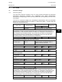
CONTENTS
Safety Section
Pxxx/EN SS/G11
Update Documentation
SS
N/A
Section 1
Introduction
P115/EN IT/A41
IT
Section 2
Technical Data
P115/EN TD/A41
TD
Section 3
Getting Started
P115/EN GS/A41
GS
Section 4
Settings
P115/EN ST/A41
ST
Section 5
Operation
P115/EN OP/B41
OP
Section 6
Application Notes
P115/EN AP/A41
Section 7
Measurements and Recording
P115/EN MR/A41
Section 8
Commissioning
P115/EN CM/A41
Section 9
Maintenance
P115/EN MT/A41
Section 10
Troubleshooting
P115/EN TS/A41
Section 11
Symbols and Glossary
P115/EN SG/A41
Section 12
Installation
P115/EN IN/B41
Section 13
Communication Database
P115/EN CT/A41
Section 14
Firmware and Service Manual
Version History
P115/EN VH/A41
AP
MR
CM
MT
TS
SG
IN
CT
VH
Pxxx/EN SS/G11
SAFETY SECTION
Pxxx/EN SS/G11
Safety Section
Page 1/8
STANDARD SAFETY STATEMENTS AND EXTERNAL
LABEL INFORMATION FOR SCHNEIDER ELECTRIC
EQUIPMENT
1.
INTRODUCTION
3
2.
HEALTH AND SAFETY
3
3.
SYMBOLS AND EXTERNAL LABELS ON THE EQUIPMENT
4
3.1
Symbols
4
3.2
Labels
4
4.
INSTALLING, COMMISSIONING AND SERVICING
4
5.
DECOMMISSIONING AND DISPOSAL
7
6.
TECHNICAL SPECIFICATIONS FOR SAFETY
8
6.1
Protective fuse rating
8
6.2
Protective Class
8
6.3
Installation Category
8
6.4
Environment
8
Pxxx/EN SS/G11
Page 2/8
Safety Section
BLANK PAGE
Pxxx/EN SS/G11
Safety Section
1.
Page 3/8
INTRODUCTION
This guide and the relevant equipment documentation provide full information on safe
handling, commissioning and testing of this equipment. This Safety Guide also includes
descriptions of equipment label markings.
Documentation for equipment ordered from Schneider Electric is despatched separately from
manufactured goods and may not be received at the same time. Therefore this guide is
provided to ensure that printed information which may be present on the equipment is fully
understood by the recipient.
The technical data in this safety guide is typical only, see the technical data section of the
relevant product publication(s) for data specific to a particular equipment.
Before carrying out any work on the equipment the user should be familiar with the
contents of this Safety Guide and the ratings on the equipment’s rating label.
Reference should be made to the external connection diagram before the equipment is
installed, commissioned or serviced.
Language specific, self-adhesive User Interface labels are provided in a bag for some
equipment.
2.
HEALTH AND SAFETY
The information in the Safety Section of the equipment documentation is intended to ensure
that equipment is properly installed and handled in order to maintain it in a safe condition.
It is assumed that everyone who will be associated with the equipment will be familiar with
the contents of that Safety Section, or this Safety Guide.
When electrical equipment is in operation, dangerous voltages will be present in certain parts
of the equipment. Failure to observe warning notices, incorrect use, or improper use may
endanger personnel and equipment and also cause personal injury or physical damage.
Before working in the terminal strip area, the equipment must be isolated.
Proper and safe operation of the equipment depends on appropriate shipping and handling,
proper storage, installation and commissioning, and on careful operation, maintenance and
servicing. For this reason only qualified personnel may work on or operate the equipment.
Qualified personnel are individuals who:
•
Are familiar with the installation, commissioning, and operation of the equipment and
of the system to which it is being connected;
•
Are able to safely perform switching operations in accordance with accepted safety
engineering practices and are authorised to energize and de-energize equipment and
to isolate, ground, and label it;
•
Are trained in the care and use of safety apparatus in accordance with safety
engineering practices;
•
Are trained in emergency procedures (first aid).
The equipment documentation gives instructions for its installation, commissioning, and
operation. However, the manual cannot cover all conceivable circumstances or include
detailed information on all topics. In the event of questions or specific problems, do not take
any action without proper authorization. Contact the appropriate Schneider Electric technical
sales office and request the necessary information.
Pxxx/EN SS/G11
Page 4/8
3.
Safety Section
SYMBOLS AND EXTERNAL LABELS ON THE EQUIPMENT
For safety reasons the following symbols and external labels, which may be used on the
equipment or referred to in the equipment documentation, should be understood before the
equipment is installed or commissioned.
3.1
Symbols
Caution: refer to equipment documentation
Caution: risk of electric shock
Protective Conductor (*Earth) terminal
Functional/Protective Conductor (*Earth)
terminal.
Note: This symbol may also be used for a
Protective Conductor (Earth) Terminal if that
terminal is part of a terminal block or subassembly e.g. power supply.
*NOTE:
3.2
THE TERM EARTH USED THROUGHOUT THIS GUIDE IS THE
DIRECT EQUIVALENT OF THE NORTH AMERICAN TERM
GROUND.
Labels
See Safety Guide (SFTY/4L M/G11) for equipment labelling information.
4.
INSTALLING, COMMISSIONING AND SERVICING
Equipment connections
Personnel undertaking installation, commissioning or servicing work for this
equipment should be aware of the correct working procedures to ensure safety.
The equipment documentation should
commissioning, or servicing the equipment.
be
consulted
before
installing,
Terminals exposed during installation, commissioning and maintenance may
present a hazardous voltage unless the equipment is electrically isolated.
The clamping screws of all terminal block connectors, for field wiring, using M4
screws shall be tightened to a nominal torque of 1.3 Nm.
Equipment intended for rack or panel mounting is for use on a flat surface of a
Type 1 enclosure, as defined by Underwriters Laboratories (UL).
Any disassembly of the equipment may expose parts at hazardous voltage, also
electronic parts may be damaged if suitable electrostatic voltage discharge (ESD)
precautions are not taken.
If there is unlocked access to the rear of the equipment, care should be taken by
all personnel to avoid electric shock or energy hazards.
Voltage and current connections shall be made using insulated crimp terminations
to ensure that terminal block insulation requirements are maintained for safety.
Watchdog (self-monitoring) contacts are provided in numerical relays to indicate
the health of the device. Schneider Electric strongly recommends that these
contacts are hardwired into the substation's automation system, for alarm
purposes.
Pxxx/EN SS/G11
Safety Section
Page 5/8
To ensure that wires are correctly terminated the correct crimp terminal and tool
for the wire size should be used.
The equipment must be connected in accordance with the appropriate connection
diagram.
Protection Class I Equipment
-
Before energizing the equipment it must be earthed using the protective
conductor terminal, if provided, or the appropriate termination of the
supply plug in the case of plug connected equipment.
-
The protective conductor (earth) connection must not be removed since
the protection against electric shock provided by the equipment would be
lost.
-
When the protective (earth) conductor terminal (PCT) is also used to
terminate cable screens, etc., it is essential that the integrity of the
protective (earth) conductor is checked after the addition or removal of
such functional earth connections. For M4 stud PCTs the integrity of the
protective (earth) connections should be ensured by use of a locknut or
similar.
The recommended minimum protective conductor (earth) wire size is 2.5 mm²
(3.3 mm² for North America) unless otherwise stated in the technical data section
of the equipment documentation, or otherwise required by local or country wiring
regulations.
The protective conductor (earth) connection must be low-inductance and as short
as possible.
All connections to the equipment must have a defined potential. Connections that
are pre-wired, but not used, should preferably be grounded when binary inputs
and output relays are isolated. When binary inputs and output relays are
connected to common potential, the pre-wired but unused connections should be
connected to the common potential of the grouped connections.
Before energizing the equipment, the following should be checked:
-
Voltage rating/polarity (rating label/equipment documentation),
-
CT circuit rating (rating label) and integrity of connections,
-
Protective fuse rating,
-
Integrity of
applicable),
-
Voltage and current rating of external wiring, applicable to the application.
the
protective
conductor
(earth)
connection
(where
Accidental touching of exposed terminals
If working in an area of restricted space, such as a cubicle, where there is a risk of
electric shock due to accidental touching of terminals which do not comply with
IP20 rating, then a suitable protective barrier should be provided.
Equipment use
If the equipment is used in a manner not specified by the manufacturer, the
protection provided by the equipment may be impaired.
Removal of the equipment front panel/cover
Removal of the equipment front panel/cover may expose hazardous live parts,
which must not be touched until the electrical power is removed.
Pxxx/EN SS/G11
Page 6/8
Safety Section
UL and CSA/CUL Listed or Recognized equipment
To maintain UL and CSA/CUL Listing/Recognized status for North America the
equipment should be installed using UL or CSA Listed or Recognized parts for
the following items: connection cables, protective fuses/fuseholders or circuit
breakers, insulation crimp terminals and replacement internal battery, as
specified in the equipment documentation.
For external protective fuses a UL or CSA Listed fuse shall be used. The Listed
type shall be a Class J time delay fuse, with a maximum current rating of 15 A
and a minimum d.c. rating of 250 Vd.c., for example type AJT15.
Where UL or CSA Listing of the equipment is not required, a high rupture
capacity (HRC) fuse type with a maximum current rating of 16 Amps and a
minimum d.c. rating of 250 Vd.c. may be used, for example Red Spot type NIT or
TIA.
Equipment operating conditions
The equipment should be operated within the specified electrical and
environmental limits.
Current transformer circuits
Do not open the secondary circuit of a live CT since the high voltage produced
may be lethal to personnel and could damage insulation. Generally, for safety,
the secondary of the line CT must be shorted before opening any connections to
it.
For most equipment with ring-terminal connections, the threaded terminal block
for current transformer termination has automatic CT shorting on removal of the
module. Therefore external shorting of the CTs may not be required, the
equipment documentation should be checked to see if this applies.
For equipment with pin-terminal connections, the threaded terminal block for
current transformer termination does NOT have automatic CT shorting on removal
of the module.
External resistors, including voltage dependent resistors (VDRs)
Where external resistors, including voltage dependent resistors (VDRs), are fitted
to the equipment, these may present a risk of electric shock or burns, if touched.
Battery replacement
Where internal batteries are fitted they should be replaced with the recommended
type and be installed with the correct polarity to avoid possible damage to the
equipment, buildings and persons.
Insulation and dielectric strength testing
Insulation testing may leave capacitors charged up to a hazardous voltage. At the
end of each part of the test, the voltage should be gradually reduced to zero, to
discharge capacitors, before the test leads are disconnected.
Insertion of modules and pcb cards
Modules and PCB cards must not be inserted into or withdrawn from the
equipment whilst it is energized, since this may result in damage.
Insertion and withdrawal of extender cards
Extender cards are available for some equipment. If an extender card is used,
this should not be inserted or withdrawn from the equipment whilst it is energized.
This is to avoid possible shock or damage hazards. Hazardous live voltages may
be accessible on the extender card.
Pxxx/EN SS/G11
Safety Section
Page 7/8
External test blocks and test plugs
Great care should be taken when using external test blocks and test plugs such
as the MMLG, MMLB and MiCOM P990 types, hazardous voltages may be
accessible when using these. *CT shorting links must be in place before the
insertion or removal of MMLB test plugs, to avoid potentially lethal voltages.
*Note: When a MiCOM P992 Test Plug is inserted into the MiCOM P991 Test
Block, the secondaries of the line CTs are automatically shorted, making
them safe.
Fiber optic communication
Where fiber optic communication devices are fitted, these should not be viewed
directly. Optical power meters should be used to determine the operation or
signal level of the device.
Cleaning
The equipment may be cleaned using a lint free cloth dampened with clean water,
when no connections are energized. Contact fingers of test plugs are normally
protected by petroleum jelly, which should not be removed.
5.
DECOMMISSIONING AND DISPOSAL
De-commissioning
The supply input (auxiliary) for the equipment may include capacitors across the
supply or to earth. To avoid electric shock or energy hazards, after completely
isolating the supplies to the equipment (both poles of any dc supply), the
capacitors should be safely discharged via the external terminals prior to
de-commissioning.
Disposal
It is recommended that incineration and disposal to water courses is avoided.
The equipment should be disposed of in a safe manner. Any equipment
containing batteries should have them removed before disposal, taking
precautions to avoid short circuits. Particular regulations within the country of
operation, may apply to the disposal of the equipment.
Pxxx/EN SS/G11
Page 8/8
6.
Safety Section
TECHNICAL SPECIFICATIONS FOR SAFETY
Unless otherwise stated in the equipment technical manual, the following data is applicable.
6.1
Protective fuse rating
The recommended maximum rating of the external protective fuse for equipments is 16A,
high rupture capacity (HRC) Red Spot type NIT, or TIA, or equivalent. Unless otherwise
stated in equipment technical manual, the following data is applicable. The protective fuse
should be located as close to the unit as possible.
CAUTION -
6.2
Protective Class
IEC 60255-27: 2005
EN 60255-27: 2006
6.3
CTs must NOT be fused since open circuiting them may
produce lethal hazardous voltages.
Class I (unless otherwise specified in the equipment
documentation). This equipment requires a protective
conductor (earth) connection to ensure user safety.
Installation Category
IEC 60255-27: 2005
Installation Category III (Overvoltage Category III):
EN 60255-27: 2006
Distribution level, fixed installation.
Equipment in this category is qualification tested at
5 kV peak, 1.2/50 µs, 500 Ω, 0.5 J, between all
supply circuits and earth and also between
independent circuits.
6.4
Environment
The equipment is intended for indoor installation and use only. If it is required for use in an
outdoor environment then it must be mounted in a specific cabinet or housing which will
enable it to meet the requirements of IEC 60529 with the classification of degree of
protection IP54 (dust and splashing water protected).
Pollution Degree - Pollution Degree 2
Altitude - Operation up to 2000m
IEC 60255-27:2005
EN 60255-27: 2006
Compliance is demonstrated by reference
to safety standards.
Introduction
P115/EN IT/A41
MiCOM P115
IT
INTRODUCTION
Date:
20th February 2009
Hardware Suffix:
A
Software Version:
1D
Connection Diagrams:
10P11504
P115/EN IT/A41
Introduction
MiCOM P115
IT
Introduction
P115/EN IT/A41
MiCOM P115
(IT) 1-1/8
CONTENTS
1.
MiCOM DOCUMENTATION STRUCTURE
3
2.
INTRODUCTION TO MiCOM
5
3.
PRODUCT SCOPE
6
3.1
Key for the manual
6
3.2
Functional overview
6
3.3
Ordering options
8
FIGURES
Figure 1:
Functional diagram of P115 with all ordering options included
7
IT
P115/EN IT/A41
(IT) 1-2/8
IT
Introduction
MiCOM P115
Introduction
P115/EN IT/A41
MiCOM P115
1.
(IT) 1-3/8
MiCOM DOCUMENTATION STRUCTURE
The manual provides a functional and technical description of the MiCOM protection relay
and a comprehensive set of instructions for the relay’s use and application.
The section contents are summarized below:
P115/EN IT
Introduction
A guide to the MiCOM range of relays and the documentation structure. Also a general
functional overview of the relay and brief application summary are given.
P115/EN TD Technical Data
Technical data including setting ranges, accuracy limits, recommended operating conditions,
ratings and performance data. Compliance with norms and international standards is quoted
where appropriate.
P115/EN GS Getting Started
A guide to the different user interfaces of the protection relay describing how to start using it.
This section provides detailed information regarding the communication interfaces of the
relay, including a detailed description of how to access the settings database stored within
the relay.
P115/EN ST Settings
List of all relay settings, including ranges, step sizes and defaults, together with a brief
explanation of each setting.
P115/EN OP Operation
A comprehensive and detailed functional description of all protection and non-protection
functions.
P115/EN AP Application Notes
This section includes a description of common power system applications of the relay,
calculation of suitable settings, some typical worked examples, and how to apply the settings
to the relay.
P115/EN MR Measurements and Recording
Detailed description of the relays recording and measurements functions.
P115/EN CM Commissioning
Instructions on how to commission the relay, comprising checks on the calibration and
functionality of the relay.
P115/EN MT Maintenance
A general maintenance policy for the relay is outlined.
P115/EN TS Troubleshooting
Advice on how to recognize failure modes and the recommended course of action. Includes
guidance on who at Schneider Electric to contact for advice.
P115/EN SG Symbols and Glossary
List of common technical abbreviations found within the product documentation.
P115/EN IN
Installation
Recommendations on unpacking, handling, inspection and storage of the relay. A guide to
the mechanical and electrical installation of the relay is provided, incorporating earthing
recommendations. All external wiring connections to the relay are indicated.
IT
P115/EN IT/A41
(IT) 1-4/8
Introduction
MiCOM P115
P115/EN CM Communication Database
This section provides an overview regarding the SCADA communication interfaces of the
relay.
P115/EN VH Firmware and Service Manual Version History
History of all hardware and software releases for the product.
IT
Introduction
P115/EN IT/A41
MiCOM P115
2.
(IT) 1-5/8
INTRODUCTION TO MiCOM
MiCOM is a comprehensive solution capable of meeting all electricity supply requirements. It
comprises a range of components, systems and services from Schneider Electric.
Central to the MiCOM concept is flexibility.
MiCOM provides the ability to define an application solution and, through extensive
communication capabilities, integrate it with your power supply control system.
The components within MiCOM are:
−
P range protection relays;
−
C range control products;
−
M range measurement products for accurate metering and monitoring;
−
S range versatile PC support and substation control packages.
MiCOM products include extensive facilities for recording information on the state and
behaviour of the power system using disturbance and fault records. They can also provide
measurements of the system at regular intervals for a control center enabling remote
monitoring and control to take place.
For up-to-date information on any MiCOM product, visit our website:
www.schneider-electric.com
IT
P115/EN IT/A41
Introduction
(IT) 1-6/8
3.
MiCOM P115
PRODUCT SCOPE
P115 is a 3 phase and earth fault non-directional overcurrent CT-powered and/or auxiliary
voltage powered protection relay (depends on the ordering option. Refer to chapter 3.3)
The scope of P115 applications covers:
IT
•
industry and distribution MV networks;
•
back-up protection in HV applications,
The relay protects one, two or three-phase applications against earth fault and phase-tophase short-circuit faults. It was especially developed for compact MV switchboards with
circuit breakers. Thanks to a built-in USB port, fault records, events and relay settings can be
downloaded to a local PC.
Settings of the protection elements are made using the front panel keyboard, with verification
via the display or using MiCOM S1 setting software.
3.1
Key for the manual
P115 relays are available with different hardware versions: number of outputs, type of a
case, different rated currents (1A or 5A), auxiliary voltage ranges, communication protocols,
etc.
Please refer to the commercial publication for further information on the product features and
application arrangements.
3.2
Functional overview
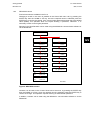
The P115 relay offers a wide variety of protection functions.
The protection features are summarized below:
PROTECTION FUNCTIONS OVERVIEW
50/51
Three non-directional overcurrent stages are provided for each phase. The
first (I>) and the second stage (I>>) may be set to Inverse Definite Minimum
Time (IDMT) or Definite Time (DT); the third stage (I>>>) may be set to DT
only.
50N/51N
Two non-directional overcurrent stages are provided. The first stage (IN>)
may be set to Inverse Definite Minimum Time (IDMT) or Definite Time (DT);
the second stage (IN>>) may be set to DT only.
46
Asymmetry overcurrent stage is provided with Definite Time (DT)
The P115 also offers the following relay management functions in addition to the functions
listed above.
•
Up to 5 last Fault Records and 100 Events available via the USB port or rear optional
communication port (RS485)
•
Readout of actual settings available via the USB port or rear communication port
(RS485)
•
Control of CB via a rear communication port (RS485) or the front panel
•
Two binary inputs
•
External trip function via binary input
•
Up to 4 output contacts (ordering option)
•
Energy output for CB low energy coil (ordering option)
Introduction
P115/EN IT/A41
MiCOM P115
(IT) 1-7/8
•
Energy output for Flag Indicator
•
3 phase current inputs
•
Earth fault current input
•
Circuit Breaker Fail (CBF) function
•
Start and trip counters
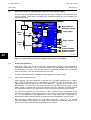
Application overview
Figure 1:
Functional diagram of P115 with all ordering options included
IT
P115/EN IT/A41
Introduction
(IT) 1-8/8
3.3
MiCOM P115
Ordering options
Information Required with Order
Relay Type
P115
746
Number of output contacts
IT
2 c/o contacts
4 c/o contacts
0
1
Energy output for CB trip
Without
Low energy CB coil: 24VDC, 0.1J
Low energy CB coil: 12VDC, 0.02J
0
1
2
Type of the case
Wall mounting
Flush mounting
0
1
Rear communication port (RS485)
Without
RS485, Switchable protocol: Modbus RTU/IEC103 (Vx and CT powering only)
0
1
Auxiliary voltage Vx range
(Vx: common for auxiliary supply voltage and binary inputs)
Vx and CT powering;
Vx= 60-240VAC/60-250VDC
Vx and CT powering;
Vx= 24-48AC/DC
CT powering only;
Vx= 60-240VAC/60-250VDC
CT powering only;
Vx= 24-48VAC/DC
0
1
2
3
E/F nominal current, setting range
(Setting range given for DT characteristic, for
IDMT refer to technical data chapter)
Ien=1A, settings: 0.01 – 2 Ien
Ien=1A, settings: 0.05 – 10 Ien
Ien=1A, settings: 0.2 – 40 Ien
Ien=5A, settings: 0.01 – 2 Ien
Ien=5A, settings: 0.05 – 10 Ien
Ien=5A, settings: 0.2 – 40 Ien
0
1
2
3
4
5
Phase nominal current, setting range
(Setting range given for DT characteristic, for
IDMT refer to technical data chapter)
In=1A, settings: 0.2 – 40 In
In=5A, settings: 0.2 – 40 In
0
1
Languages
English/Polish/German/French/Spanish
English/Czech/Slovak/Hungarian/Turkish
1
2
Technical Data
P115/EN TD/A41
MiCOM P115
TD
TECHNICAL DATA
Date:
20th February 2009
Hardware Suffix:
A
Software Version:
1D
Connection Diagrams:
10P11504
P115/EN TD/A31
(TD) 2-2/8
TD
Technical Data
MiCOM P115
Technical Data
P115/EN TD/A41
MiCOM P115
(TD) 2-1/8
Technical Data
Ratings
Mechanical Specifications
AC Measuring Inputs
Nominal frequency of fundamental harmonic:
50 to 60 Hz
(fn):
Operating range of fundamental harmonic:
40 to 70 Hz
Design
Wall mounting case or flush mounting case.
Enclosure Protection
EN 60529: 1991
IP 40 Protection for relay housing
IP 20 Protection for terminals.
IP 52 Protection (front panel) against dust and
dripping water for flash mounted case.
Connection: refer to section 12 of P115
Installation chapter (P115/EN IN)
Weight
approx. 1 kg
Nominal burden per phase:
In=1A: < 2.5 VA at In
In=5A: < 3 VA at In
Thermal withstand:
Continuous 3 In
for 10 s: 30 In
for 1 s; 100 In
Terminals
AC Current Input Terminals
Threaded M3 screw-type plug-in terminals,
with wire protection for conductor cross-section
(i) 0.2 - 6 mm2 single-core
(ii) 0.2 - 4 mm2 finely stranded
General Input/Output Terminals
For power supply, binary and contact inputs,
output contacts and COM for rear
communications.
Threaded M3 screw-type plug-in terminals,
with wire protection for conductor cross-section
(i) 0.2 - 4 mm2 single-core
(ii) 0.2 - 2.5 mm2 finely stranded
Local communication
USB port
Cable Type: USB 2.0
Connectors:
(i) PC: type A male
(ii) P115: type mini B male
Rear Communications Port
EIA(RS)485 signal levels, two wire
Connections located on general purpose block,
M3 screw
For screened twisted pair cable, distance to be
bridged: multi-endpoint link: max. 100 m
Isolation to SELV level.
Phase current
Nominal current (In): 1 or 5 A (ordering option)
RMS measurement in range: 40 Hz -1 kHz
Earth fault current
Nominal current (Ien): 1 or 5 A (ordering
option)
RMS measurement in range:
40 Hz -70 Hz
Nominal burden:
In=1A: < 2.5 VA at Ien
In=5A: < 3 VA at Ien
Thermal withstand:
Continuous: 3 Ien
for 10 s: 30 Ien
for 1 s: 100 Ien
Minimum level of current required for relay
powering
Phase current <0.2In, approx.:
- one phase:
0.17 In
- two phases:
0.1 In
- three phases: 0.06 In
Earth fault current: <0.2 Ien, approx. 0.17 Ien
Note: depends on connection to the terminals,
the earth fault input supplies P115 (connection:
terminals 7 and 9) or does not supply P115
(connection: terminals 8 and 9) (refer to
Installation chapter: P115/EN IN)
Note: if the sum of the currents (which power
the P115) is below 0.5In (example of sum
equal to 0.5In= Ia: 0.25In + Ib: 0.25In+ Ic: 0In +
IN: 0Ien) the LED indications, the display and
the RS485 comms are switched off. RL2, RL3,
RL4 are not energized. Depending on the
setting, the earth current is included or not in
the above sum (refer to Settings chapter:
P115/EN ST).
TD
P115/EN TD/A41
Technical Data
(TD) 2-2/8
MiCOM P115
Binary Inputs
Power Supply
The binary inputs can be powered with both
DC and AC voltage as binary input control
voltage
Nominal Auxiliary Voltage Vx
Two ordering options:
(i) Vx: 24 to 48 Vdc, and 24 to
48 Vac (50/60 Hz)
Binary input type:
(ii) Vx: 60 to 250 Vdc, and 60 to
240 Vac (50/60 Hz)
TD
Operating Range
(i) 19 to 58 V (dc), 19 to 53V (ac)
(ii) 48 to 300 V (dc), 48 to 265 V (ac)
With a tolerable ac ripple of up to 12% for a dc
supply, per IEC 60255-11: 1979.
Nominal Burden
Auxiliary Power Supply Vx
Note:
(i) Initial position: no output nor LED
energized.
(ii) Active position: all outputs and LEDs
energized.
(i) for ac max. approx.:
Vx
V
24-48Vac
60-240Vac
24
48
48
60
100/110
220/230
264
S
VA
Initial
position
3.1
2.4
2.6
2.7
3.1
5.1
6.1
Active
position
5.5
6.0
5.5
5.2
5.7
7.4
8.4
(ii) for dc Vx voltage (24-48Vdc
and 60-250Vdc ) max. approx:
Initial position: 1.5W
Active position: 3.7W
Power-up Time for Auxiliary Supply Voltage
only
Time to power up via auxiliary supply only (not
powered by CT): < 0.04 s.
Auxiliary Power Supply Voltage Interruption
(without powering by CT)
IEC 60255-11: 1979
The relay will withstand a 50 ms interruption
of the DC auxiliary supply within the auxiliary
supply range, without de-energizing.
EN 61000-4-11: 1997
The relay will withstand a 50 ms interruption
in an AC auxiliary supply, without
de-energizing.
Current transformer
Detailed information and CT requirements are
given in the Application chapter (P115/EN AP)
Optically isolated
Rated nominal voltage: the same as Vx
Operating range:
the same as Vx
Withstand:
300 Vdc or 275 Vac
Nominal pick-up and reset thresholds:
(i) for DC:
- Vx=24-48Vac/dc:
- Pick-up:
approx. 12 Vdc
- Reset:
approx. 11 Vdc
- Vx=60-240Vac/dc:
- Pick-up:
approx. 21 Vdc
- Reset:
approx. 20 Vdc
(ii) for AC:
- Vx=24-48Vac/dc:
- Pick-up:
approx. 16 Vac
- Reset:
approx. 11 Vac
- Vx=60-240Vac/dc:
- Pick-up:
approx. 26 Vac
- Reset:
approx. 19 Vac
Recognition time: <20 ms
Energy consumption of binary inputs:
Resistance of binary inputs:
(i) 24 to 48 Vac/dc: 5,5kΩ ±5%
(ii) 60 to 240 Vac/dc: 100kΩ ±5%
For 220Vdc: (220Vdc)2 x 100kΩ±5% =
0.484W±5%
Outputs
Impulse Output for the tripping coil
(ordering option)
Trip energy:
- Hardware version P115746x1xxxxxx:
E ≥ 0.1 J, 24 Vdc -0% to +10%
- Hardware version P115746x2xxxxxx::
E ≥ 0.02 J, 12 Vdc -0% to +10%
Impulse Output for flag indicator or
auxiliary relay
Trip energy: E ≥ 0.01 J
Voltage: 24 Vdc -0% to +10%
Note: The tripping energy for the tripping
coil/flag indicator is stored by a capacitor
built into the protection relay. The
capacitors are loaded by a current or the
auxiliary voltage. The duration of the trip
pulse is 50 ms. The pause between the
individual pulses depends on the
impedance of the tripping coil/flag
indicator coil/flag indicator and on the
current level. The pulse lasts as long as
the activation threshold is exceeded.
Technical Data
MiCOM P115
P115/EN TD/A41
(TD) 2-3/8
Output Contacts
General purpose relay outputs for signaling,
tripping and alarming:
Rated voltage:
250 V
Continuous current:
5A
Short-duration current: 25 A for 3 s
Making capacity:
150 A for 30 ms
Breaking capacity:
DC: 50 W resistive
DC: 25 W inductive (L/R = 40 ms)
AC: 1250 VA resistive (cos φ = unity)
AC: 1250 VA inductive (cos φ = 0.7)
Response to command: < 10 ms
Durability:
Loaded contact: 10 000 operations
minimum,
Unloaded contact: 100 000 operations
minimum.
Impulse Voltage Withstand Test
EN 60255-27:2005,
Front time: 1.2 µs, Time to half-value: 50 µs,
Peak value: 5 kV
Source Characteristics: 500 Ohm, 0.5J.
Common and differential mode - power supply,
terminal block (excluding RS485), binary
inputs, relays.
Environmental Conditions
Immunity to Electrostatic Discharge
IEC 60255-22-2: 1996, Class 3,
8kV discharge in air to all communication
ports.
6kV point contact discharge to any part of
the front of the product.
Ambient Temperature Range
EN 60255-6: 1994
Operating temperature range:
-20°C to +60°C (or -4°F to +140°F).
Temporary permissible temperature -40°C to
+85°C (-85°F to +185°F) with additional errors
Storage and transit:
-25°C to +70°C (or -13°F to +158°F).
Ambient Humidity Range
IEC 60068-2-78: 2001:
56 days at 93% relative humidity and +40°C
Per EN 60068-2-30: 2005:
Damp heat cyclic, six (12 + 12) hour cycles,
93% RH, +25 to +55°C
Type Tests
Insulation
EN 60255-5: 2001
Insulation resistance > 100MΩ at 500 Vdc
(Using only electronic/brushless insulation
tester).
Creepage Distances and Clearances
EN 60255-27:2005
Pollution degree 2,
Overvoltage category III,
Impulse test voltage 5 kV.
High Voltage (Dielectric) Withstand
EN 60255-27:2005, 2 kV r ms AC, 1 minute:
Between all case terminals connected
together, and the case earth.
Between all terminals of independent circuits
with terminals on each independent circuit
connected together.
Electromagnetic Compatibility
(EMC)
1 MHz Burst High Frequency Disturbance
Test
IEC 60255-22-1: 2005, Class III,
Common-mode test voltage: 2.5 kV,
Differential test voltage: 1.0 kV,
Test duration: 2s, Source impedance: 200Ω
Electrical Fast Transient or Burst
Requirements
EN 60255-22-4: 2002. Test severity Class III:
Amplitude: 2 kV, burst frequency 5 kHz
(Class III),
Surge Immunity Test
EN60255-22-5:2002; EN 61000-4-5: 2006
Level 3,
Time to half-value: 1.2/50 µs,
Amplitude: 2kV between all groups and case
earth,
Amplitude: 1kV between terminals of each
group.
Immunity to Radiated Electromagnetic
Energy
EN 60255-22-3: 2000, Class III:
Test field strength, frequency band 80 to
1000 MHz:
10 V/m,
Test using AM: 1 kHz / 80%,
Radiated Immunity from Digital Radio
Telephones
EN 60255-22-3:2000
10 V/m, 900 MHz 100% AM, 200 Hz/50%
square wave
Immunity to Conducted Disturbances
Induced by Radio Frequency Fields
EN 61000-4-6: 1996, Level 3,
Disturbing test voltage: 10 V, 150 Hz to
80 MHz, 80% AM, 1 kHz
TD
P115/EN TD/A41
Technical Data
(TD) 2-4/8
Power Frequency Magnetic Field Immunity
IEC 61000-4-8: 1994, Level 4,
30 A/m applied continuously,
300 A/m applied for 3 s.
Conducted Emissions
EN 55022: 2006
0.15 - 0.5 MHz, 79 dBμV (quasi peak)
66 dBμV (average)
0.5 - 30 MHz, 73 dBμV (quasi peak)
60 dBμV (average).
TD
Radiated Emissions
EN 55022: 2006
30 - 230 MHz, 40 dBμV/m at 10 m
measurement distance
230 - 1 GHz, 47 dBμV/m at 10 m
measurement distance.
EU Directives
EMC Compliance
2004/106/EC:
Compliance to the European Commission
Directive on EMC is claimed. Product Specific
Standards were used to establish conformity:
EN50263: 2000
Product Safety
2006/95/EC:
Compliance with European Commission Low
Voltage Directive.
Compliance is demonstrated by reference to
product safety standard:
EN60255-27:2005
Mechanical Robustness
Vibration Test
EN 60255-21-1: 1996
Response Class 1
Endurance Class 1
Shock and Bump
EN 60255-21-2: 1996
Shock response Class 1
Shock withstand Class 1
Bump Class 1
MiCOM P115
Protection Functions
Note: All settings and measurements are given
as a multiple of the In (Ien) current value
(ordering option)
Operation time
The typical operation time, if the P115 is
supplied from Vx or if the current is above
0.2 In (Ien): ≤ 40ms
If the pre-fault current is below 0.2 In (Ien) in all
phases and that there is no Vx on the 11 -12
terminals, additional time correction should be
applied for the operation time (measured on
the outputs contacts):
(i) Hardware ver. P115746x0xxxxxx
(without energy output for low energy
tripping coil) for all types of fault
(1, 2, 3-phases):
≤ 25mA,
except 1-phase fault, where the current
is below 1.6 In (Ien)
≤ 30mA,
(ii) Hardware ver. P115746x1xxxxxx (with
energy output for low energy tripping coil
24VDC 0.1Ws) and P115746x2xxxxxx
(with energy output for low energy
tripping coil 12VDC 0.02Ws):
- for faults where the current is ≤ 0.6 In
(Ien):
1-phase fault: ≤ 60ms
2-phase fault: ≤ 60ms
3-phase fault: ≤ 30ms
- for all types of fault where the current is
> 0.6 In (Ien) (1, 2, 3-phases): ≤ 30ms
The correction time measured on energy
outputs is 6ms shorter than that measured on
output contacts.
Note: The tripping time in case of a fault if the
pre-fault current is below 0.2 In and
there is no auxiliary voltage (Vx) on
terminals 11 -12 is the sum of the set
time delay, the operation time and the
correction time (see above).
Protection Accuracy
Note:
1. All data below are given for inception of
fault from currents above 0.2 In (Ien) at
least in 1 phase or if the P115 is powered
from the Vx auxiliary voltage supply.
If the pre-fault current is below 0.2 In (Ien)
in all phases and that there is no Vx on
terminals 11 -12 additional time correction
should be taken into account (see above)
2. Reference Conditions:
Sinusoidal signals with nominal frequency
fn, total harmonic distortion ≤ 2 %, ambient
temperature 20 °C and nominal auxiliary
voltage Vx
Technical Data
P115/EN TD/A41
MiCOM P115
Three-Phase Overcurrent I>, I>>
(i) Pick-up: Setting ±5%
in the temperature range -20°C to +60°C
(ii) Pick-up: Setting ±7.5%
in the temperature range -40°C to +85°C
Drop-off: 0.95 x setting ±5%
Minimum IDMT level:
1.05 x setting ±5%
IDMT curve: ±7.5% or 30 ms whichever is
greater
DT operation: ±2% or 30 ms, whichever is
greater
DT reset: ±7.5% or 30 ms, whichever is greater
(TD) 2-5/8
(ii) Setting ±7.5%
in the temperature range -40°C to +85°C
DT operation:
±2% or 30 ms whichever is greater
DT reset: ±7.5% or 30 ms, whichever is
greater
Measured Data Acquisition
Reference Conditions:
Sinusoidal signals with nominal frequency fn
total harmonic distortion ≤2 %, ambient
temperature 20 °C and nominal auxiliary
voltage Vx.
Three-Phase Overcurrent I>>>
(i) Pick-up: Setting ±5%
in the temperature range -20°C to +60°C
(ii) Pick-up: Setting ±7.5%
in the temperature range -40°C to +85°C
Deviation relative to the relevant nominal value
under reference conditions
Drop-off: 0.95 x setting ±5%
DT operation: ±2% or 30 ms, whichever is
greater
DT reset: ±7.5% or 30 ms, whichever is greater
Phase and earth current:
Asymmetry current:
Operating Data
For current up to 3 In (Ien):
±3%
±5%
Fault Data
Earth Fault IN>
(i) Pick-up: Setting ±5%
in the temperature range -20°C to +60°C
Phase and earth current :
For current ≤ 3 In (Ien):
±5%
For current > 3 In (Ien):
±5% of
measured current value
(ii) Pick-up: Setting ±7.5%
in the temperature range -40°C to +85°C
Communications
Drop-off: 0.95 x setting ±5%
Minimum IDMT level:
1.05 x setting ±5%
IDMT curve: ±7.5% or 30 ms whichever is
greater
DT operation: ±2% or 30 ms, whichever is
greater
DT reset: ±7.5% or 30 ms, whichever is greater
USB:
USB port for local communications with a PC
Protocol: MODBUS RTU
The virtual COM port for USB comms should
be set in as follows:
(i) Address: 1
(ii) Baud Rate: 115.2 kbits/s
Earth Fault IN>>
Pick-up:
(i) Setting ±5%
in the temperature range -20°C to +60°C
(iii) Comms. Mode:
Data Bit: 8
Stop bit: 1
Parity: none
(ii) Setting ±7.5%
in the temperature range -40°C to +85°C
RS485:
DT operation:
±2% or 30 ms whichever is greater
DT reset: ±10% or 30 ms, whichever is greater
Asymmetry Overcurrent Protection
Measurement criteria based on the maximum
deviation of the phase current to the average
value of the three-phase current
Pick-up:
(i) Setting ±5%
in the temperature range -20°C to +60°C
Protocol (ordering option):
- MODBUS RTU
- IEC 103
Physical Link: Copper; RS485 half duplex
Comms. Mode:
Data Bits: 8
Stop bit: 1 or 2
(default: 1)
Parity: no parity/Odd parity/Even parity
(default: Even parity)
Address: 1 to 127 (default: 1)
Baud Rate: 4.8 kbits/s to 115.2 kbits/s
(default: 19.2 kbit/s)
TD
P115/EN TD/A41
Technical Data
(TD) 2-6/8
Settings, Measurements and
Records List
Ground Overcurrent
(Earth Fault)
Settings
Stages:
IN> Function:
Phase Overcurrent
DT, TD time delay:
0.00 s to 200 s; steps: 0.01 s,
I>, I>> Function:
TMS: 0.02 s to 1.6 s: steps: 0.01 s
DT, TD time-delay:
0.02 s to 200 s; steps: 0.01 s,
TMS: 0.02 s to 1.6 s: steps: 0.01 s
TD
MiCOM P115
Type of characteristics:
(i) DT
(ii) IEC S Inverse
(iii) IEC V Inverse
(iv) IEC E Inverse
(iii) UK LT Inverse
(iv) RC
(vi) RI
(vii) UK ST Inverse
(viii) UK Rectifier Inverse
(ix) IEEE M Inverse
(x) IEEE V Inverse
(xi) IEEE E Inverse
(xii) US CO2
(xiii) US CO8
The mathematical formulae and curves for the
twelve Inverse Time characteristics available
with the P115 are presented in the Operation
chapter (P115/EN OP) of this manual.
IDMT accuracy is ensured up to 20 x In
Reset time:
- DT delayed
- IDMT delayed for IEEE, US, IEC stages
only: according to the mathematical
formulae presented in Operation chapter
(P115 EN OP) of this manual
I>, I>> Current Set: 0.2 to 4 In steps: 0.01 In
I>>> Function:
Type of characteristic: DT
DT time delay: 0.00 s to 200 s; steps: 0.01 s
I>>> Current Set: 0.2 to 40 In steps: 0.01 In
Type of characteristic:
(i)
DT
(ii)
IEC S Inverse
(iii) IEC V Inverse
(iv) IEC E Inverse
(v) UK LT Inverse
(vi) RC
(vi) RI
(xiv) UK ST Inverse
(xv) UK Rectifier Inverse
(xvi) IEEE M Inverse
(xvii) IEEE V Inverse
(xviii) IEEE E Inverse
(xix) US CO2
(xx) US CO8
The mathematical formulae and curves for the
twelve Inverse Time characteristics available
with the P115 are presented in the Operation
chapter (P115/EN OP) of this manual
Reset time:
- DT delayed
- IDMT delayed for IEEE, US, IEC stages
only: according to the mathematical
formulae presented in Operation chapter
(P115 EN OP) of this manual
IN> Current Set (ordering option):
(i) 0.01 to 0.2 Ien step 0.01 Ien
(ii) 0.05 to 1 Ien steps: 0.01 Ien,
(iii) 0.2 to 4 Ien steps: 0.01 Ien,
IDMT accuracy is ensured up to 20 x current
setting
IN>> Function:
Type of characteristic: DT
DT time delay: 0.00 s to 200 s steps: 0.01 s
IN>> Current Set:
(i) 0.01 to 2 Ien steps: 0.01 Ien
(ii) 0.05 to 10 Ien steps: 0.01 Ien
(iii) 0.2 to 40 Ien steps: 0.1 Ien
Minimum earth current to supply P115: 0.2 Ien
Technical Data
MiCOM P115
P115/EN TD/A41
(TD) 2-7/8
Asymmetry Overcurrent
Iasym> Function:
Iasym> Current Set: 0.08 to 4 In steps: 0.01 In
DT time delay:
0.02s to 200 s steps: 0.01 s
Circuit Breaker Fail
CB Fail Timer: 0.00 to10.00 s steps: 0.01 s
I< Current Set: 0.05 to 4 In steps: 0.01 In
IN< Current Set: 0.05 to 4 Ien steps: 0.01 Ien,
CBF Prot. Reset:
I< and IN<
Measurements List
Measurements
IA, IB, IC, IN
TD
P115/EN TD/A41
(TD) 2-8/8
TD
Technical Data
MiCOM P115
Getting Started
P115/EN GS/A41
MiCOM P115
GS
GETTING STARTED
Date:
20th February 2009
Hardware Suffix:
A
Software Version:
1D
Connection Diagrams:
10P11504
P115/EN GS/A41
Getting Started
MiCOM P115
GS
Getting Started
MiCOM P115
P115/EN GS/A41
(GS) 3-1/24
CONTENTS
1.
GETTING STARTED
3
1.1
User interfaces and menu structure
3
1.2
Introduction to the relay
3
1.2.1
Front panel
3
1.3
Relay connection and power-up
6
1.3.1
Auxiliary Supply Voltage (Vx) connection
7
1.3.2
Current inputs
7
1.3.3
Tripping coil output (ordering option)
7
1.3.4
Flag indicator output
7
1.3.5
Earthing
8
1.3.6
Output contacts
8
1.3.7
Binary inputs
8
1.4
Introduction to the user interfaces and settings options
8
1.5
Changing parameters via the front panel.
8
1.5.1
SETTING CHANGE MODE
10
1.6
P115 Menu description
13
1.6.1
Headers
13
1.6.2
ALARM STATUS column
13
1.6.3
RECORDS column
15
1.6.4
SETTTING GROUP columns
16
1.6.5
GLOBAL SETTINGS column
17
1.6.6
COMMISIONING column
17
1.6.7
SETTING CHANGE MODE column
18
1.6.8
Menu Map
19
GS
P115/EN GS/A41
(GS) 3-2/24
Getting Started
MiCOM P115
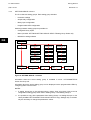
FIGURES
GS
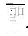
Figure 1: P115 front panel
5
Figure 2: Rear view of the P115
6
Figure 3: Column headers
13
Figure 4: ALARM column
14
Figure 5: RECORDS column
15
Figure 6: SETTING GROUP 1 columns
16
Figure 7: GLOBAL SETTINGS column
17
Figure 8: COMMISSIONING column
17
Figure 9: SETTING CHANGE MODE column
18
Figure 10: P115 Menu Map - Page 1
19
Figure 11: P115 Menu Map - Page 2
20
Figure 12: P115 Menu Map - Page 3
21
Figure 13: P115 Menu Map - Page 4
22
Figure 14: P115 Menu Map - Page 5
23
Figure 15: P115 Menu Map - Page 6
24
Getting Started
P115/EN GS/A41
MiCOM P115
1.
(GS) 3-3/24
GETTING STARTED
Before carrying out any work on the equipment, the user should be familiar
with the contents of the Safety Guide SFTY/4L M/E11 or later issue, OR
the safety and technical data section of the technical manual and also the
ratings on the equipment rating label.
For safety reasons, no work must be carried out on the P115 until all
power sources to the unit have been disconnected.
1.1
User interfaces and menu structure
The settings and functions of the MiCOM protection relay can be accessed both from the
front panel keypad and LCD, and via the front and rear communication ports. Information on
each of these methods is given in this section to describe how to start using the relay.
1.2
Introduction to the relay
1.2.1
Front panel
The front panel of the relay is shown in Figure 1.
The front panel of the relay includes:
-
a 16-character by 2-line alphanumeric liquid crystal display (LCD)
-
a 7-key keypad comprising 4 arrow keys, an enter key, a clear key, a read key,
-
8 LEDs
a USB port for local communication.
1.2.1.1
Indications
Fixed Function LEDS:
Healthy – Powering of microprocessor and no hardware problems detected (green LED)
Trip – Any Trip by protection criteria
And 6 programmable LEDS for the following functions (OR logic):
I> –
Start of the first phase overcurrent stage
I>> –
Start of the second phase overcurrent stage
I>>>–
Start of the third phase overcurrent stage
IN> –
Start of the first e/f overcurrent stage
IN>> –
Start of the second e/f overcurrent stage
Iasym> – Start of the asymmetry overcurrent stage
AUX1 –
Trigger of AUX1 timer (via a binary input)
AUX2 –
Trigger of AUX2 timer (via a binary input)
tI> –
Trip of the first phase overcurrent stage (flashing: start)
tI>> –
Trip of the second phase overcurrent stage (flashing: start)
tI>>> –
Trip of the third phase overcurrent stage (flashing: start)
tIN> –
Trip of the first e/f overcurrent stage (flashing: start)
GS
P115/EN GS/A41
Getting Started
(GS) 3-4/24
MiCOM P115
tIN>> –
Trip of the second e/f overcurrent stage (flashing: start)
tIasym> –
Trip of the asymmetry overcurrent stage (flashing: start)
tAUX1 –
Time delay tAUX1 elapsed (flashing: start)
tAUX2 –
Time delay tAUX1 elapsed (flashing: start)
CBF fail –
Trip of Circuit Breaker Failure function
CB ext. –
Trigger of external trip
tCB not Healthy –
Input configured to this function detects a problem with CB (for
example spring problem, too low pressure etc.). Signaling is active
after settable time delay (tCB; GLOBAL SETTINGS/CIRCUIT
BREAKER/ tCB not Healthy)
Setting Group 1 (2) – Setting Group 1 (2) active
GS
Start Phase A –
Start of the phase overcurrent stage (set to trip) in phase A
Start Phase B –
Start of the phase overcurrent stage (set to trip) in phase B
Start Phase C –
Start of the phase overcurrent stage (set to trip) in phase C
Start Earth –
Start of the e/f overcurrent stage (set to trip)
Every LED can be configured to be latching or self-resetting (SETTING GROUP 1/ LEDS
CONFIGURATION G1/ Latched LEDs)
If LED is configured for latching, the resetting mode can be set:
-
LEDs reset by manual reset (GLOBAL SETTINGS/LOC/LEDs Reset by Start 0:No)
-
LEDs reset by any protection start (set for CB tripping) or manual reset (GLOBAL
SETTINGS/LOC/LEDs Reset by Start 1:Yes)
External indication of a fault can be made via an external Flag Indicator (available in
Schneider Electric offer: FI10) which should be connected to terminals 27-28.
Getting Started
P115/EN GS/A41
MiCOM P115
(GS) 3-5/24
1
2
3
4
5
6
7
8
9
10
11
12
13
1 - Green “Healthy” LED.
2 - Red “Trip” LED Any trip of protection
3, 4, 5, 6, 7, 8 - Red programmable LED.
9 - 16-character by 2-line alphanumeric liquid crystal display (LCD)
10 - A clear key
11 - A read key,
12 - 4 arrow keys, an enter key
13 - USB port for local connection
Figure 1: P115 front panel
GS
P115/EN GS/A41
Getting Started
(GS) 3-6/24
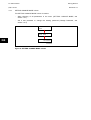
MiCOM P115
14
15
GS
16
17
rd
14 - 3 terminal block: Auxiliary voltage supply, Binary inputs, Binary
outputs, Flag indicator energy output, Low energy trip coil,
nd
15 - 2 terminal block: RS485
st
16 - 1 terminal block: phase and e/f current inputs
17 - PCT Protective (Earth) Conductor terminal
Figure 2: Rear view of the P115
1.3
Relay connection and power-up
The relay can be powered from the following sources:
-
Current input phase L1 (A)
-
Current input phase L2 (B)
-
Current input phase L3 (C)
-
E/F Current input (N) (depends on connection on the terminals)
-
Auxiliary voltage Vx (terminals 11-12)
-
USB port (some electronic boards only, to ensure HMI, USB and/or RS485
communication only)
Getting Started
P115/EN GS/A41
MiCOM P115
1.3.1
(GS) 3-7/24
Auxiliary Supply Voltage (Vx) connection
Before applying the auxiliary supply voltage to the relay, check that the rated nominal ac or
dc voltage is appropriate for the application and that it will be connected to the correct
terminals (11&12). The relay's serial number, current rating, and power rating information
can be viewed on the upper side of the case. The ac or dc supply voltage must be within the
corresponding nominal range of the device, as indicated in the table below, for the
appropriate nominal rating of the equipment:
Nominal ranges of auxiliary
voltage Vx
Operative dc Range
Operative ac Range
24 to 48 Vac/dc
19 to 58 Vdc
19 to 53 Vac
60 to 250 Vdc and
60 to 240 Vac
48 to 300 Vdc
48 to 265 Vac
Once the ratings have been verified for the application, connect the equipment to an external
power source capable of delivering the requirements specified on the label, to perform the
relay familiarization procedures. Please refer to the wiring diagrams in the Installation
section for complete installation details, ensuring that the correct polarities are observed in
the case of dc supply.
Note:
1.3.2
The label specifies Vx for both the P115 supply input and binary
inputs.
Current inputs
The measuring current inputs of the P115 should be connected to the secondary wires of the
power system CTs as shown in the connection diagrams in section 8 of P115 Installation
chapter P115/EN IN.
The parameters of the CTs which can be connected to the P115’s current input terminals are
detailed in section 3 of chapter P115/EN AP - Applications.
1.3.3
Tripping coil output (ordering option)
Terminals 29 and 30 (3rd block terminal) are used for the connection of the CB's low energy
tripping coil (ordering option)
The trip energy is provided by capacitors built into the P115. The trip command is a 50 ms
pulse and its repetition depends on the tripping coil's impedance and on the current value.
Repetition continues until the tripping current criteria are reset.
The trip voltage on terminals 29 and 30 depends on the ordering option:
1.3.4
-
24 Vdc, trip energy ≥ 0.1 Ws
-
12 Vdc, trip energy ≥ 0.02 Ws
Flag indicator output
Terminals 27 and 28 (3rd block terminal) are used for the connection of an external flag
indicator.
The flag indicator can be used for trip signaling. The flag indicator output is supplied from a
built -in capacitor different from the trip coil output (terminals 29 and 30).
The trip command is a 50ms pulse, its repetition depends on the external relay's impedance
(flag indicator coil) and on the current value. Repetition continues until the tripping current
criteria are reset.
The voltage on terminals 27 and 28 is greater than 24 Vdc. The trip energy is greater than
0.01 Ws.
GS
P115/EN GS/A41
Getting Started
(GS) 3-8/24
1.3.5
MiCOM P115
Earthing
Terminal “PCT” is the Protective (Earth) Conductor Terminal which must be permanently
connected for safety reasons (refer to Figure 2).
1.3.6
Output contacts
P115 has 2 or 4 output contacts depending on ordering option.
P115 is delivered with the following default factory settings for outputs:
GS
-
output RL1 (N/O: 16-17, N/C: terminals 16-18) is configured to Protection Trip, without
latching of output
-
output RL2 (N/O: 19-20, N/C: terminals 19-21 ) is not configured
-
output RL3 (N/O: terminals 22-23) (optional) is not configured.
-
output RL4 (N/O: 24-25 terminals) (optional) is not configured.
To change the output configuration refer to section 1.2.3 of chapter P115/EN ST - Settings .
The output connection diagram is shown in section 8 of chapter P115/EN IN - Installation.
1.3.7
Binary inputs
The P115 has 2 binary inputs: L1 (terminals 13-15) and L2 (terminals 14-15)
The P115 is delivered with the following default factory settings for inputs:
-
input L1 is not configured.
-
input L2 is not configured.
To change input configuration refer to section 1.2.3 of chapter P115/EN ST - Settings.
The input connection diagram is shown in section 8 of chapter P115/EN IN - Installation.
1.4
Introduction to the user interfaces and settings options
The relay has a USB user interface for MiCOM S1 software.
By using this interface it is possible to download the setting values, last 5 fault records and
make a full configuration of P115
NOTE:
After connection to the USB port the “Healthy” LED is lit. If the LED is
not lit refer to chapter P115/EN TS - Troubleshooting.
The USB port integrates electronic boards only to allow communications with the P115 via
the HMI/RS485/USB interfaces.
1.5
Changing parameters via the front panel.
Changing of all parameters is password-protected.
After restart or applying of power supply, the P115 is in Protection Mode. This means that all
settings are the same as in the relay's operation system and are available on the front
panel.
To change any parameters, it is necessary to switch the P115 to the SETTING CHANGE
MODE.
The SETTING CHANGE MODE is indicated by the sequential flashing of the programmable
LEDs (from 3 up to 8 LEDs) on the front panel.
Until it is switched back from the SETTING CHANGE MODE to the PROTECTION MODE, or
restarted by disconnecting then reconnecting the power supply, the P115 uses the setting
parameters that were active before the SETTING CHANGE MODE was entered (previous
settings).
Getting Started
P115/EN GS/A41
MiCOM P115
(GS) 3-9/24
Press the ENTER key after changing a chosen parameter (confirmation of change). The new
value is saved in FRAM memory but the P115 still uses the setting value which was active
before the SETTING CHANGE MODE was entered (previous settings). The new value will
be available in the operation system only after the firmware has been reset. When the
firmware is reset, all the settings stored in FRAM memory are loaded into the P115 system.
When switching from the SETTING CHANGE MODE to the PROTECTION MODE, a warm
reset is applied.
The P115 therefore applies the new parameters to the relay's operation system.
Afterwards, the settings available on the front panel those used by the operation system are
coherent.
NOTE:
While the LEDs are flashing (SETTING CHANGE MODE) there can
be a mismatch between the settings displayed on the front panel and
those used by the operating system.
The password protection of the relay comprises three levels:
•
Administrator (Without limits)
•
Protection setting (Protection only)
•
Control only (Test control)
Administrator rights: all the menu settings may be changed.
Protection setting rights: it is possible to change settings in the PROTECTION column, CB
control and reset of the counters are also possible.
Control rights: CB control from the front panel only.
For each level the password consists of 5 digits (0 to 9)
The default password is 00000.
If the first password is different, this means that the ‘Administrator’ password has been
changed.
The Protection setting password is still 00000. Therefore, to protect settings against
unauthorized access it is necessary to change the Protection setting password by first
entering 00000 then a new value.
The Control password is still 00000. Therefore, if it is necessary to change it, first enter
00000 then the new value (Control right) of the password.
NOTES:
1.
If the Protection setting rights have not been changed, or if it has been
set to the default value (00000), it is possible to change all the settings
in the PROTECTION column, reset the counters and control the CB
without entering a password, simply by pressing the ENTER key. This
makes it possible to change a chosen parameter by automatically
switching the P115 to the SETTING CHANGE MODE (the
programmable LEDs are flashing).
This means that even after changing only one parameter it is
necessary to switch the P115 back to PROTECTION MODE in order
to activate the new settings (warm restart).
2.
If the Control rights password has not been changed or if it has been
set to the default value (00000) it is possible to control the CB or
choose the older faults in Fault Record column without password
protection.
GS
P115/EN GS/A41
Getting Started
(GS) 3-10/24
1.5.1
MiCOM P115
SETTING CHANGE MODE
The SETTING CHANGE MODE should be used to change settings.
Using the SETTING CHANGE MODE ensures that all changed parameters will be applied
simultaneously so as to avoid any problems caused by possible setting inconsistencies.
The SETTING CHANGE MODE makes it possible to change settings while the relay is active
without any risk (the P115 continues to use the previous settings).
After exiting the SETTING CHANGE MODE a warm reset of firmware is applied so that all
the protection counters are reset.
NOTE:
Latched LEDs and outputs are not reset (stored values are not
cleared during a P115 reset)
To switch the P115 to SETTING CHANGE MODE navigate to the SETTING CHANGE
MODE main header (see Figure 9), then press the DOWN key:
GS
Edit settings?
Enter PSWD
Press ENTER key
Edit settings?
Enter PSWD 00000
The 0 digit furthest to the right is flashing.
Enter the password:
1. If the digit is flashing, change the digit to the required value by pressing the DOWN key
or the UP key.
2. Change the flashing digit by pressing the left key or right key.
3. Continue as above to set the whole password (5 digits)
4. If the correct password is set, press the ENTER key
The LCD displays 'OK' during approximately 1 second, then the new SETTING CHANGE
cell is displayed:
If the password entered is for:
- Administrator rights:
Setting change:
Without limits
- Protection settings:
Setting change:
Without limits
- Control only:
Setting change:
Test control
The screen displays the scope of the current modification rights. To indicate that the P115 is
in SETTING CHANGE MODE the programmable LEDs are flashing.
At this time it is possible to start changing the setting parameters.
Getting Started
P115/EN GS/A41
MiCOM P115
(GS) 3-11/24
NOTE:
The parallel pressing: UP and LEFT key it makes jump from any place
to:
Edit settings?
Enter PSWD
the menu cell in which the password can be entered (hot key).
If all settings are changed, it is necessary to return to PROTECTION MODE to apply a warm
reset.
Press the UP and LEFT keys simultaneously to jump to the following cell:
Edit settings?
Exit:press ENTER
Press the ENTER key to apply a warm reset and display the following cell:
Setting change:
Protected
The programmable LEDs do not flash sequentially. The P115 is in PROTECTION MODE
NOTE:
In SETTING CHANGE MODE all functions use the previously stored
settings (before the SETTING CHANGE MODE was entered).
Changing of a single setting parameter
Go to the required setting cell (see section 1.5.1).
Press the ENTER key.
Edit settings?
Enter PSWD 00000
Using the LEFT, RIGHT, UP, DOWN keys, enter the password (see section 1.5.1).
Press ENTER to confirm the password and switch to SETTING CHANGE MODE.
Press ENTER to enter the chosen setting parameter.
Using the LEFT, RIGHT, UP, DOWN keys, set the required value.
Confirm the change by pressing the ENTER key.
Switch from SETTING CHANGE MODE to PROTECTION MODE (see section 1.5.1).
For example, press the LEFT and UP keys simultaneously to display the following cell:
Edit settings?
Exit:press ENTER
Press the ENTER key to switch from SETTING CHANGE MODE to PROTECTION MODE.
The following cell should be displayed:
Setting change:
Protected
The above cell confirms that settings are password-protected, and that the P115 is in
PROTECTION MODE.
Additionally the programmable LEDs do not flash sequentially.
GS
P115/EN GS/A41
(GS) 3-12/24
Getting Started
MiCOM P115
Changing the password
To change the password, first enter the existing password to obtain the appropriate
password protection rights.
Press the DOWN key to display the following cell:
Change Password
Press the ENTER key, to display:
Change Password
00000
Using the LEFT, RIGHT, UP, DOWN keys, enter the new password.
GS
Press ENTER to confirm the new password and jump to the cell displaying information on
protection rights
For example:
Setting change:
Without limits
To exit the SETTING CHANGE MODE (apply a warm reset) press the LEFT and UP keys
simultaneously to display the following cell:
Edit settings?
Exit:press ENTER
Press the ENTER key to confirm switching from SETTING CHANGE MODE to
PROTECTION MODE.
The following cell should be displayed:
Setting change:
Protected
The above cell confirms that the settings are password-protected and that the P115 is in
PROTECTION MODE. Additionally the programmable LEDs do not flash sequentially.
Getting Started
P115/EN GS/A41
MiCOM P115
(GS) 3-13/24
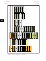
1.6
P115 Menu description
1.6.1
Headers
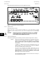
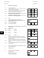
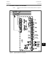
The main headers are shown in Figure 3.
CB status:Opened
CTRL: no operat.
000.0A
000.0A
000.0A
000.0A
MEASUREMENTS
00.00In 00.00In
00.00In 00.00Ien
ALARM STATUS
RECORDS
SETTING GROUP 1
OP PARAMETERS
SETTING CHANGE
MODE
COMMISSIONING
GLOBAL SETTINGS
SETTING GROUP 2
P0857ENa
Figure 3: Column headers
1.6.2
ALARM STATUS column
ALARM STATUS (see Figure 4) information is available if the cause of alarm has been
triggered. Therefore, if after pressing the DOWN key no the new cell is displayed, it means
that no alarms have been detected.
Depending on the P115 configuration an alarm signal is self-resetting (no cause of alarm –
no alarm signal; GLOBAL SETTINGS/LOC/Alarm Display 0: Self-Reset) or manually
resettable (alarm signal latched; GLOBAL SETTINGS/LOC/Alarm Display 1: Manual Reset).
Default setting: 0: Self-Reset. This means that if an alarm signal has disappeared no
information is available in the ALARM STATUS column.
If Manual Reset is set, this means that if an alarm signal has disappeared the corresponding
information is still available in the ALARM STATUS column up until it is reset in the ALARM
STATUS/ Alarm Reset cell.
Alarm information is always available in the event recorder. However, the programmable
LEDs can be used to store causes of alarm if required.
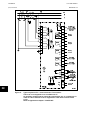
Figure 4 shows all causes of alarms (if alarms have been enabled in the main configuration
column of the protection function).
GS
P115/EN GS/A41
Getting Started
(GS) 3-14/24
MiCOM P115
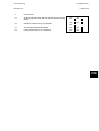
ALARM STATUS
Alarm
I>
Alarm
I>>
Alarm
I>>>
Alarm
IN>
Alarm
GS
IN>>
Alarm
Iasym>
Alarm
CB Fail
Alarm
tAUX1
Alarm
tAUX2
Alarm
CB not Healthy
Alarm
Hardware Warning
Alarm Reset
No operation
P0858ENb
Figure 4: ALARM column
Getting Started
P115/EN GS/A41
MiCOM P115
1.6.3
(GS) 3-15/24
RECORDS column
Five fault records are available in the P115.
Changing a record in the menu is possible in the Record Nb menu cell, by pressing the
ENTER key then the DOWN or UP key. Once the required record is selected, press the
ENTER key to confirm the change. If the Control rights password has been set to the default
value (00000), this operation does not require entering a password, otherwise it is
necessary to enter Control rights password.
Records in the Fault Recorder can be reset using the MiCOM S1 communication software or
via the RS485 link.
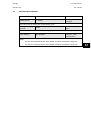
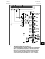
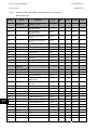
RECORDS
FAULT RECORDS
COUNTERS
Record Nb
1:Fault 1
Trips Nb
Trip
Fault Trips Nb
00000
No fault
GS
00000
Fault Time
00:00:00.000
Fault Start Nb
00000
Fault Date
01/01/08
Alarm Nb
Active Set Group
Group 1
HW Warnings Nb
00000
Fault Origin
None
Counter Reset [C]
No operation
IA=
IB=
0000.0A
0000.0A
IC=
IN=
0000.0A
0000.0A
00000
P0859ENa
Figure 5: RECORDS column
Counters can be reset in the Counter Reset cell of the menu, by pressing the ENTER key
then the DOWN or UP key. Once the required record is selected, press the ENTER key to
confirm the change. This operation requires entering an Administrator password.
In addition, counters can be reset using the MiCOM S1 communication software or via the
RS485 link.
P115/EN GS/A41
Getting Started
(GS) 3-16/24
1.6.4
MiCOM P115
SETTTING GROUP columns
The P115 has two setting groups. Each setting group includes:
-
Protection settings
-
Output relay configuration
-
Binary input configuration
-
Programmable LED configuration
Switching between setting groups is possible via:
GS
-
Configured binary inputs
-
Menu (GLOBAL SETTINGS/SETTING GROUP SELECT/Setting Group Select cell)
-
MiCOM S1 setting software
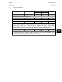
SETTING GROUP 1
PROTECTION G1
PHASE O/C G1
[50/51]
OUTPUT RELAYS
CONFIGURATION G1
INPUTS
CONFIGURATION G1
LEDS
CONFIGURATION G1
Latched
outputs
Reverse
Input Logic
21
00
Latched
LEDs
876543
000000
Reverse
4321
outp. logic 0000
Blocked
Outputs
21
00
Protect.
Trip
876543
000000
Protect.
Trip
TF4321
000000
Reset
Latchd LEDs
21
00
Alarm
876543
000000
Any Trip
(pulse)
F4321
00000
Reset
Latchd Outp
21
00
Start
I>
876543
000000
4321
0000
E/GND FAULT G1
[50/51N]
ASYMMETRY G1
[46]
CB Fail
[50BF]
G1
AUX TIMERS
G1
P0860ENa
Figure 6: SETTING GROUP 1 columns
Information about the active setting group is available in menu: OP PARAMETERS/
Active Set Group cell.
Information about the active setting group can be displayed via the programmable LEDs by
configuring them to that function.
NOTES:
1. If setting groups are to be switched using a binary input, this binary input must be
configured to setting group switch both in Setting Group 1 and Setting Group 2.
2. It is possible to copy all the parameters from Setting Group 1 to Setting Group 2 or vice
versa (GLOBAL SETTINGS/SETTING GROUP SELECT/Copy Settings cell). It will then
only be necessary to change the parameters' values.
Getting Started
P115/EN GS/A41
MiCOM P115
1.6.5
(GS) 3-17/24
GLOBAL SETTINGS column
Global Settings include all general settings, such as:
-
Localization (LOC)
-
Setting Group operation (SETTING GROUP SELECT)
-
Current transformer parameters (CT RATIO)
-
Time settings related to Circuit Breaker control or monitoring (CIRCUIT BREAKER)
-
RS485 communication parameters (COMMUNICATION)
GLOBAL SETTINGS
LOC
SETTING GROUP
SELECT
CT RATIO
CIRCUIT BREAKER
COMMUNICATION
Language
0: English
Setting Group
1: Group 1
Line CT primary
00000A
tOpen pulse min
00.00s
Protocol
0:Modbus
Default Display
0: Meas. In
t Change Setting
G1->G2
000.00s
Line CT Sec
In=1A
tClose Pulse
0.00s
Relay Address
001
Copy settings
No operation
E/Gnd CT Primary
00000A
tP Pulse
Baud Rate
0:4800
00000min
P0861ENb
Figure 7: GLOBAL SETTINGS column
It is possible to Copy all parameters from Setting Group 1 to Setting Group 2 and inversely in
Copy settings cell by pressing the ENTER key. Choose the required operation by pressing
the UP or DOWN key (Copy G1 Æ G2 or Copy G2 Æ G1). Confirm the change by pressing
the ENTER key.
Note: The setting group change time-delay, from Setting Group 1 to Setting Group 2
(t Change Setting cell), applies to changes effected via a binary input only.
1.6.6
COMMISIONING column
In the COMISSIONING column displays the active binary input and binary output status.
COMMISSIONING
Opto I/P
Status
21
00
Relay O/P TF4321
Status
000000
Test
Pattern
TF4321
000000
Test outputs
0: no operation
P0862ENb
Figure 8: COMMISSIONING column
GS
P115/EN GS/A41
Getting Started
(GS) 3-18/24
1.6.7
MiCOM P115
SETTING CHANGE MODE column
The SETTING CHANGE MODE column is used to:
-
Allow changing of all parameters in the menu (SETTING CHANGE MODE, see
section 1.5.1)
-
Set a new password or change the existing password (Change Password, see
section 1.5.3)
SETTING CHANGE
MODE
Edit settings?
Enter PSWD
GS
Setting change:
Protected
P0863ENa
Figure 9: SETTING CHANGE MODE column
21
00
Figure 10: P115 Menu Map (Firmware: 1D) - Page 1
TF4321
000000
Test outputs
0: no operation
Test
Pattern
Relay O/P TF4321
Status
000000
Opto I/P
Status
COMMISSIONING
Setting change:
Protected
Edit settings?
Enter PSWD
SETTING CHANGE
MODE
000.0A
00.00In
000.0A
00.00Ien
000.0A
00.00In
IC=
IN=
Iasym=
Hardware Version
00
Active Set Group
1:Group 1
13:15:33
06/08/01
00.00In 00.00In
00.00In 00.00Ien
000.0A
000.0A
Alarm Reset
No operation
ALARM STATUS
MiCOM P115
Time
Date
Schneider
Electric
AREVA
Software Version
1D
000.0A
00.00In
000.0A
00.00In
IA=
MEASUREMENTS
IB=
Reference
Description
P115
OP PARAMETERS
000.0A
000.0A
1.6.8
CB status:Opened
CTRL: no operat.
Getting Started
P115/EN GS/A41
(GS) 3-19/24
Menu Map
GS
Figure 11: P115 Menu Map (Firmware: 1D) - Page 2
0000.0A
0000.0A
Counter Reset
No operation
Fault Origin
None
IC=
IN=
HW Warnings Nb
00000
Active Set Group
Group 1
0000.0A
0000.0A
00000
Alarm Nb
Fault Date
06/08/01
IA=
IB=
Fault Start Nb
00000
000.00s
2: Alarm
000.00s
000.00s
tIN>>
000.00s
IN>> Threshold
0.00Ien
IN>> ?
1:Trip
DMT tReset
IN>
000.00s
Reset Delay Type
IN>
0: DMT
IN> TMS
tIasym>
Delay Type
IN> 1: IEC SI
000.00s
Iasym> Threshold
0.00In
Iasym>?
2: Alarm
IN> Threshold
0.00Ien
IN> ?
1:Trip
ASYMMETRY G1
[46]
G1
IN< Threshold
CBF
0.00Ien
I< Threshold
CBF
0.00In
CB Fail Time tBF
00.00s
CB Fail?
1: Trip
CB Fail
[50BF]
G1
000.00s
tAUX2?
000.00s
AUX2?
2: Alarm
tAUX1
AUX1?
2: Alarm
AUX TIMERS
(GS) 3-20/24
tI>>>
I>>> Threshold
00.00In
I>>>?
I>>?
0: Disabled
DMT tReset
I>
000.00s
Reset Delay Type
I>
0: DMT
tI>
Delay Type
I>
0: DMT
I> Threshold
00.00In
1: Trip
E/GND FAULT G1
[50/51N]
GS
Fault Time
12:05:23:42
I>?
Fault Trips Nb
00000
Trip
No fault
PHASE O/C G1
[50/51]
Trips Nb
Record Nb
1:Fault 1
00000
PROTECTION G1
COUNTERS
SETTING GROUP 1
FAULT RECORDS
RECORDS
P115/EN GS/A41
Getting Started
MiCOM P115
tAUX1
TF4321
000000
tI>>
tI>>>
F4321
00000
F4321
00000
4321
0000
4321
0000
4321
0000
4321
0000
4321
0000
4321
0000
Any Trip
(pulse)
Alarm
Start
I>
Start
I>>
Start
I>>>
Start
IN>
Figure 12: P115 Menu Map (Firmware: 1D) - Page 3
Start
IN>>
Start
Iasym>
CBF ext.
CB Fail
tIasym>
tIN>>
tIN>
tI>
TF4321
000000
Protect.
Trip
Start
Earth
Start
Phase C
4321
0000
4321
0000
4321
0000
Start
Phase B
TF4321
000000
TF4321
000000
4321
0000
F4321
00000
F4321
00000
TF4321
000000
4321
0000
4321
0000
TF4321
000000
Start
Phase A
Hardware
Warning
tCB not
Healthy
Trip
CB
Close
CB
Trip
pulse tP
tAUX2
TF4321
000000
TF4321
000000
TF4321
000000
TF4321
000000
TF4321
000000
TF4321
000000
4321
0000
Start
AUX2
Reverse
4321
outp. logic 0000
Blocking
Iasym>
Blocking
IN>>
Blocking
IN>
Blocking
I>>>
Blocking
I>>
Blocking
I>
Reset
Latchd Outp
Reset
Latchd LEDs
Blocked
Outputs
21
00
21
00
21
00
21
00
21
00
21
00
21
00
21
00
21
00
21
00
Reverse
Input Logic
4321
0000
Start
AUX1
Latched
outputs
4321
0000
INPUTS
CONFIGURATION G1
OUTPUT RELAYS
CONFIGURATION G1
876543
000000
876543
000000
Alarm
Start
I>
Start
I>>
Start
I>>>
21
00
21
00
21
00
21
00
21
00
21
00
21
00
21
00
AUX1
AUX2
CBF ext.
CB status
52A
CB status
52B
CB not
Healthy
Setting
Group 2
Start
Earth
876543
000000
876543
000000
tI>>
tI>>>
876543
000000
876543
000000
Start
Phase C
876543
000000
Start
AUX2
tI>
876543
000000
Start
AUX1
876543
000000
876543
000000
Setting
Group 1
Start
Phase B
876543
000000
tCB not
Healthy
876543
000000
876543
000000
tAUX2
876543
000000
876543
000000
876543
000000
876543
000000
876543
000000
876543
000000
876543
000000
876543
000000
876543
000000
876543
000000
tAUX1
CBF ext.
CB Fail
tIasym>
tIN>>
tIN>
Start
Phase A
Start
Iasym>
Start
IN>>
Start
IN>
876543
000000
876543
000000
876543
000000
Blocking
CB Fail
Protect.
Trip
21
00
876543
000000
Blocking
AUX2
Latched
LEDs
21
00
Blocking
AUX1
LEDS
CONFIGURATION G1
Getting Started
P115/EN GS/A41
MiCOM P115
(GS) 3-21/24
GS
Figure 13: P115 Menu Map (Firmware: 1D) - Page 4
2: Alarm
000.00s
tIN>>
000.00s
IN>> Threshold
0.00Ien
IN>> ?
1:Trip
DMT tReset
IN>
000.00s
Reset Delay Type
IN>
0: DMT
G2
IN< Threshold
CBF
0.00Ien
I< Threshold
CBF
0.00In
CB Fail Time
00.00s
CB Fail?
1: Trip
CB Fail
[50BF]
G2
000.00s
tAUX2?
000.00s
AUX2?
2: Alarm
tAUX1
AUX1?
2: Alarm
AUX TIMERS
(GS) 3-22/24
tI>>>
I>>> Threshold
00.00In
I>>>?
I>>?
0: Disabled
DMT tReset
I>
000.00s
Reset Delay Type
I>
0: DMT
000.00s
IN> TMS
000.00s
tI>
000.00s
tIasym>
Delay Type
IN> 1: IEC SI
Delay Type
I>
0: DMT
Iasym>?
2: Alarm
Iasym> Threshold
0.00In
IN> ?
1:Trip
ASYMMETRY G2
[46]
IN> Threshold
0.00Ien
1: Trip
E/GND FAULT G2
[50/51N]
GS
I> Threshold
00.00In
I>?
PHASE O/C G2
[50/51]
PROTECTION G2
SETTING GROUP 2
P115/EN GS/A41
Getting Started
MiCOM P115
tAUX1
TF4321
000000
tI>>
tI>>>
F4321
00000
F4321
00000
4321
0000
4321
0000
4321
0000
4321
0000
4321
0000
4321
0000
Any Trip
(pulse)
Alarm
Start
I>
Start
I>>
Start
I>>>
Start
IN>
Figure 14: P115 Menu Map (Firmware: 1D) - Page 5
Start
IN>>
Start
Iasym>
CBF ext.
CB Fail
tIasym>
tIN>>
tIN>
tI>
TF4321
000000
Protect.
Trip
Start
Earth
Start
Phase C
4321
0000
4321
0000
4321
0000
Start
Phase B
TF4321
000000
TF4321
000000
4321
0000
F4321
00000
F4321
00000
TF4321
000000
4321
0000
4321
0000
TF4321
000000
Start
Phase A
Hardware
Warning
tCB not
Healthy
Trip
CB
Close
CB
Trip
pulse tP
tAUX2
TF4321
000000
TF4321
000000
TF4321
000000
TF4321
000000
TF4321
000000
TF4321
000000
4321
0000
Start
AUX2
Reverse
4321
outp. logic 0000
Blocking
Iasym>
Blocking
IN>>
Blocking
IN>
Blocking
I>>>
Blocking
I>>
Blocking
I>
Reset
Latchd Outp
Reset
Latchd LEDs
Blocked
Outputs
21
00
21
00
21
00
21
00
21
00
21
00
21
00
21
00
21
00
21
00
Reverse
Input Logic
4321
0000
Start
AUX1
Latched
outputs
4321
0000
INPUTS
CONFIGURATION G2
OUTPUT RELAYS
CONFIGURATION G2
876543
000000
876543
000000
Alarm
Start
I>
Start
I>>
Start
I>>>
21
00
21
00
21
00
21
00
21
00
21
00
21
00
21
00
AUX1
AUX2
CBF ext.
CB status
52A
CB status
52B
CB not
Healthy
Setting
Group 2
Start
Earth
876543
000000
876543
000000
tI>>
tI>>>
MiCOM P115
876543
000000
876543
000000
Start
Phase C
876543
000000
Start
AUX2
tI>
876543
000000
Start
AUX1
876543
000000
876543
000000
Setting
Group 2
Start
Phase B
876543
000000
tCB not
Healthy
876543
000000
876543
000000
tAUX2
876543
000000
876543
000000
876543
000000
876543
000000
876543
000000
876543
000000
876543
000000
876543
000000
876543
000000
876543
000000
tAUX1
CBF ext.
CB Fail
tIasym>
tIN>>
tIN>
Start
Phase A
Start
Iasym>
Start
IN>>
Start
IN>
876543
000000
876543
000000
876543
000000
Blocking
CB Fail
Protect.
Trip
21
00
876543
000000
Blocking
AUX2
Latched
LEDs
21
00
Blocking
AUX1
LEDS
CONFIGURATION G2
Getting Started
P115/EN GS/A41
(GS) 3-23/24
GS
Figure 15: P115 Menu Map (Firmware: 1D) - Page 6
E/Gnd CT Primary
00000A
Copy settings
No operation
LEDs Reset by
Start 0:No
IN connection
0:terminals:7-9
E/Gnd CT Sec
Ien=1A
Line CT Sec
In=1A
t Change Setting
G1->G2
000.00s
Default Display
0: Meas. In
Alarm Display
0: Self-Reset
Line CT primary
00000A
Setting Group
1: Group 1
CT RATIO
Language
0: English
SETTING GROUP
SELECT
tCB not Healthy
000s
tP Pulse
00000min
tClose Pulse
0.00s
tOpen pulse min
00.00s
CIRCUIT BREAKER
GS
LOC
GLOBAL SETTINGS
0:Modbus
Stop bits
0:one stop bit
Parity
0:No parity
Baud Rate
2:19200
Relay Address
001
Protocol
COMMUNICATION
P115/EN GS/A41
Getting Started
(GS) 3-24/24
MiCOM P115
Settings
P115/EN ST/A41
MiCOM P115
ST
SETTINGS
Date:
20th February 2009
Hardware Suffix:
A
Software Version:
1D
Connection Diagrams:
10P11504
P115/EN ST/A41
Settings
MiCOM P115
ST
Settings
P115/EN ST/A41
MiCOM P115
(ST) 4-1/32
CONTENTS
1.
GENERAL INFORMATION
3
2.
SETTINGS
5
2.1
Protection settings
5
2.1.1
Phase O/C [50/51]
5
2.1.2
E/Gnd Fault [50N/51N]
7
2.1.3
Asymmetry [46]
8
2.1.4
CB Fail [50BF]
9
2.1.5
AUX Timers
10
2.2
Configuration of the output relays
11
2.3
Configuration of the inputs
17
2.4
Configuration of the LEDs
20
3.
GLOBAL SETTINGS
24
3.1
LOC
24
3.2
SETTING GROUP SELECT
25
3.3
CT RATIO
26
3.4
CIRCUIT BREAKER
27
3.5
COMMUNICATION
28
4.
COMMISIONING
29
5.
SETTING CHANGE MODE
30
6.
OP PARAMETERS
31
ST
P115/EN ST/A41
(ST) 4-2/32
ST
Settings
MiCOM P115
Settings
P115/EN ST/A41
MiCOM P115
1.
(ST) 4-3/32
GENERAL INFORMATION
The P115 must be configured to the system and application by means of the appropriate
settings. This section gives instructions for determining the settings, which are located in the
folder entitled, Schneider Electric in the menu tree. The order in which the settings are listed
and described in this chapter is: the protection settings, control and configuration settings
(see section P115/EN GS for the detailed relay menu map). The relay is supplied with a
factory-set configuration of default settings.
All current settings refer to nominal current (ordering option: 1 A or 5 A). The nominal
current can be defined separately for phase (In) and earth (Ien) currents in the ordering
process (ordering hardware option).
MiCOM S1 can be used to download and upload protection and configuration setting values
via the relay's USB port.
The protection and I/O settings include all the following items that become active once
enabled in the configuration column of the relay menu database:
−
Protection element settings.
−
Output settings
−
Input settings
−
LED settings
There are two groups of protection and I/O settings, with each group containing the same
setting cells. One group of protection and I/O settings is selected as the active group, and is
used by the protection elements. The settings for group 1 are shown. The settings are
discussed in the same order in which they are displayed in the menu.
The menu structure is as follows:
- DEFAULT WINDOW (Currents in multiples of In, currents in Amps, CB Control window)
- ALARM STATUS
- RECORDS
- FAULT RECORDS
- COUNTERS
- SETTING GROUP 1
- PROTECTION G1
- PHASE O/C G1 [50/51]
- E/GND FAULT G1 [50N/51N]
- ASYMMETRY G1 [46]
- CB FAIL G1 [50BF]
- AUX TIMERS G1
- OUTPUT RELAY CONFIGURATION G1
- INPUTS CONFIGURATION G1
- LEDS CONFIGURATION G1
ST
P115/EN ST/A41
Settings
(ST) 4-4/32
MiCOM P115
- SETTING GROUP 2
- PROTECTION G2
- PHASE O/C G2 [50/51]
- E/GND FAULT G2 [50N/51N]
- ASYMMETRY G2 [46]
- CB FAIL G2 [50BF]
- AUX TIMERS G2
- OUTPUT RELAY CONFIGURATION G2
- INPUTS CONFIGURATION G2
- LEDS CONFIGURATION G2
- GLOBAL SETTINGS
- LOC
ST
- SETTING GROUP SELECT
- CT RATIO
- CIRCUIT BREAKER
- COMMUNICATION
- COMMISIONING
- SETTING CHANGE MODE
- OP PARAMETERS
- MEASUREMENTS
Settings
P115/EN ST/A41
MiCOM P115
(ST) 4-5/32
2.
SETTINGS
2.1
Protection settings
2.1.1
Phase O/C [50/51]
The overcurrent protection included in the P115 relay provides three-stage non-directional
three-phase overcurrent protection with independent time delay characteristics.
All overcurrent settings apply to all of the three phases but are independent for each of the
three stages.
The first two overcurrent stages have time-delayed characteristics which are selectable
between inverse definite minimum time (IDMT), or definite time (DMT). The third stage has
definite time characteristics only.
Menu Text
I> ?
Setting Range
Default Setting
Disabled
Min.
Max.
Step Size
Disabled, Enable Trip, Enable Alarm
Setting for Disable or enable of protection element.
It is possible to enable for tripping CB (Enable Trip) or enable for an Alarm signal only
(Enable Alarm). If the protection element is “Enable Trip” configured it means that it is set
to the General Trip Command ("Protect. Trip"), which can be used in I/O configuration.
If the protection element is “Enable Alarm” it means that it is set to the General Alarm
Command ("Alarm"), which can be used in I/O configuration.
I> Threshold
1.4 x In
0.2 x In
4.0 x In
0.01 x In
Pick-up setting for first stage of the overcurrent element.
I> Delay Type
IEC SI
DMT, IEC SI, IEC VI, IEC EI, UK LTI,
UK STI, UK RC, RI, IEEE MI, IEEE VI,
IEEE EI, US CO2, US CO8
Setting for the tripping characteristic for the first stage overcurrent element.
tI>
1s
0.02s
200s
0.01s
Setting for the time-delay for the definite time setting if selected for first stage element.
I> TMS
1
0.02
1.6
0.01
Setting for the time multiplier setting to adjust the operating time of the IEC, UK, and RI
IDMT characteristic
I> Time Dial
1
0.02
200
0.01
Setting for the time multiplier setting to adjust the operating time of the IEEE/US IDMT
curves.
Reset Delay Type I>
DMT
DMT or IDMT
N/A
Setting to determine the type of reset/release characteristic of the IEEE/US curves.
DMT tReset I>
0s
0s
200s
0.01s
Setting that determines the reset/release time for definite time reset characteristic.
I>> ?
Disabled
Disabled, Enable Trip, Enable Alarm
Setting for Disable or enable of protection element.
It is possible to enable for tripping CB (Enable Trip) or enable for an Alarm signal only
(Enable Alarm). If the protection element is “Enable Trip” configured it means that it is set
to the General Trip Command ("Protect. Trip"), which can be used in I/O configuration.
If the protection element is “Enable Alarm” it means that it is set to the General Alarm
Command ("Alarm"), which can be used in I/O configuration.
I>> Threshold
1.4 x In
0.2 x In
Pick-up setting for second stage of the overcurrent element.
4.0 x In
0.01 x In
ST
P115/EN ST/A41
Settings
(ST) 4-6/32
MiCOM P115
Menu Text
Delay Type I>>
Setting Range
Default Setting
IEC SI
Min.
Max.
Step Size
DMT, IEC SI, IEC VI, IEC EI, UK LTI, UK
STI, UK RC, RI, IEEE MI, IEEE VI, IEEE
EI, US CO2, US CO8
Setting for the tripping characteristic for this stage overcurrent element.
tI>>
1
0.02
200
0.01
Setting for the time-delay for the definite time setting if selected for this stage element.
I>> TMS
1
0.02
1.6
0.01
Setting for the time multiplier setting to adjust the operating time of the IEC, UK, and RI
IDMT characteristic.
I>> Time Dial
1
0.02
200
0.01
Setting for the time multiplier setting to adjust the operating time of the IEEE/US IDMT
curves.
ST
Reset Delay Type
I>>
DMT
DMT or IDMT
N/A
Setting to determine the type of reset/release characteristic of the IEEE/US curves.
DMT tReset I>>
0s
0s
200s
0.01s
Setting that determines the reset/release time for definite time reset characteristic.
I>>> ?
Disabled
Disabled, Enable Trip, Enable Alarm
Setting for Disable or enable of protection element.
It is possible to enable for tripping CB (Enable Trip) or enable for an Alarm signal only
(Enable Alarm). If the protection element is “Enable Trip” configured it means that it is set
to the General Trip Command ("Protect. Trip"), which can be used in I/O configuration.
If the protection element is “Enable Alarm” it means that it is set to the General Alarm
Command ("Alarm"), which can be used in I/O configuration.
I>>> Threshold
4 x In
0.2 x In
40.0 x In
0.1 x In
200s
0.01s
Pick-up setting for third stage of the overcurrent element.
tI>>>
0.1s
0s
Setting for the time-delay for the definite time setting if selected for this stage element.
Settings
P115/EN ST/A41
MiCOM P115
2.1.2
(ST) 4-7/32
E/Gnd Fault [50N/51N]
The earth fault element operates from earth fault current that is measured directly from the
system; either by means of a separate CT located in a power system earth connection or via
a residual connection of the three line CT's.
All overcurrent settings are independent for each of the two stages.
The first stage of e/f non-directional overcurrent protection has time-delayed characteristics
which are selectable between inverse definite minimum time (IDMT), or definite time (DMT).
The second stage has definite time characteristics only.
Menu Text
IN> ?
Setting Range
Default Setting
Disabled
Min.
Step Size
Max.
Disabled, Enable Trip, Enable Alarm
Setting for Disable or enable of protection element.
It is possible to enable for tripping CB (Enable Trip) or enable for an Alarm signal only
(Enable Alarm). If the protection element is “Enable Trip” configured it means that it is set
to the General Trip Command ("Protect. Trip"), which can be used in I/O configuration.
If the protection element is “Enable Alarm” it means that it is set to the General Alarm
Command ("Alarm"), which can be used in I/O configuration.
IN> Threshold
0.1 x Ien
0.01 x Ien
0.2 x Ien
0.01 x Ien
Pick-up setting for first stage e/f overcurrent element.
For dynamic range (ordering option): 0.01-2Ien, where Ien: nominal current for e/f input.
IN> Threshold
0.5 x Ien
0.05 x Ien
1.0 x Ien
0.01 x Ien
Pick-up setting for first stage overcurrent element.
For dynamic range (ordering option): 0.05-10Ien, where Ien: nominal current for e/f input.
IN> Threshold
1 x Ien
0.2 x Ien
4.0 x Ien
0.01 x Ien
Pick-up setting for first stage e/f overcurrent element.
For dynamic range (ordering option): 0.2-40Ien, where Ien: nominal current for e/f input.
Delay Type IN>
IEC SI
DMT, IEC SI, IEC VI, IEC EI, UK LTI,
UK STI, UK RC, RI, IEEE MI, IEEE VI,
IEEE EI, US CO2, US CO8
Setting for the tripping characteristic for the first stage e/f overcurrent element.
tIN>
1s
0.02s
200s
0.01s
Setting for the time-delay for the definite time setting if selected for first e/f stage element.
IN> TMS
1
0.02
1.6
0.01
Setting for the time multiplier setting to adjust the operating time of the IEC, UK, and RI
IDMT characteristic.
IN> Time Dial
1
0.02
200
0.01
Setting for the time multiplier setting to adjust the operating time of the IEEE/US IDMT
curves.
Reset Delay Type
IN>
DMT
DMT or IDMT
N/A
Setting to determine the type of reset/release characteristic of the IEEE/US curves.
DMT tReset IN>
0s
0s
200s
0.01s
Setting that determines the reset/release time for definite time reset characteristic.
ST
P115/EN ST/A41
Settings
(ST) 4-8/32
MiCOM P115
Menu Text
IN>> ?
Setting Range
Default Setting
Disabled
Min.
Max.
Step Size
Disabled, Enable Trip, Enable Alarm
Setting for Disable or enable of protection element.
It is possible to enable for tripping CB (Enable Trip) or enable for an Alarm signal only
(Enable Alarm). If the protection element is “Enable Trip” configured it means that it is set
to the General Trip Command ("Protect. Trip"), which can be used in I/O configuration.
If the protection element is “Enable Alarm” it means that it is set to the General Alarm
Command ("Alarm"), which can be used in I/O configuration.
IN>> Threshold
0.5 x Ien
0.01 x Ien
2.0 x Ien
0.01 x Ien
Pick-up setting for second stage of the e/f overcurrent element.
For dynamic range (ordering option): 0.01-2Ien, where Ien: nominal current for e/f input.
IN>> Threshold
2.5 x Ien
0.05 x Ien
10.0 x Ien
0.01 x Ien
Pick-up setting for second stage of the overcurrent element.
For dynamic range (ordering option): 0.05-10Ien, where Ien: nominal current for e/f input.
ST
IN>> Threshold
5 x Ien
0.2 x Ien
40.0 x Ien
0.1 x Ien
Pick-up setting for second stage of the e/f overcurrent element.
For dynamic range (ordering option): 0.2-40Ien, where Ien: nominal current for e/f input.
tIN>>
0.1s
0s
200s
0.01s
Setting for the time-delay for the definite time setting if selected for this stage.
2.1.3
Asymmetry [46]
Menu Text
Iasym> ?
Setting Range
Default Setting
Disabled
Min.
Max.
Disabled, Enable Trip,
Enable Alarm
Step Size
N/A
Setting for Disable or enable of asymmetry element.
It is possible to enable for tripping CB (Enable Trip) or enable for an Alarm signal only
(Enable Alarm).
If the protection element is “Enable Trip” configured it means that it is set to the General
Trip Command ("Protect. Trip"), which can be used in I/O configuration.
If the protection element is “Enable Alarm” it means that it is set to the General Alarm
Command ("Alarm"), which can be used in I/O configuration.
Iasym> Threshold
0.2 x In
0.08 x In
4 x In
0.01 x In
200 s
0.01 s
Pick-up setting for the asymmetry overcurrent element.
tIasym
10 s
0s
Setting for the operating time-delay for the asymmetry overcurrent element.
Settings
P115/EN ST/A41
MiCOM P115
2.1.4
(ST) 4-9/32
CB Fail [50BF]
This function consists of a circuit breaker fail function that can be initiated by:
•
Current based protection elements
•
External protection element: CBF ext..
For current-based protection, the reset condition is based on undercurrent operation to
determine whether the CB has opened.
It is common practice to use low set undercurrent elements in protection relays to indicate
that circuit breaker poles have interrupted the fault or load current, as required.
Menu Text
CBF ?
Setting Range
Default Setting
Disabled
Min.
Max.
Step Size
Disabled, Enable Trip, Enable Alarm
Setting to enable or disable the circuit breaker supervision function.
CB Fail Time tBF
0.2 s
0s
10 s
0.01 s
Setting for the circuit breaker fail timer stage for which the initiating condition must be valid.
I< Threshold CBF
0.1 x In
0.05 x In
4 x In
0.01 x In
Setting that determines the circuit breaker fail timer reset current for overcurrent based
protection circuit breaker fail initiation.
IN< Threshold CBF
0.1 x Ien
0.01 x Ien
2 x Ien
0.01 x Ien
Setting that determines the circuit breaker fail timer reset current for earth fault current
based protection circuit breaker fail initiation.
For dynamic range (ordering option): 0.01-2Ien, where Ien: nominal current for e/f input
IN< Threshold CBF
0.1 x Ien
0.05 x Ien
10 x Ien
0.01 x Ien
Setting that determines the circuit breaker fail timer reset current for earth fault current
based protection circuit breaker fail initiation.
For dynamic range (ordering option): 0.05-10Ien, where Ien: nominal current for e/f input
IN< Threshold CBF
0.1 x Ien
0.05 x Ien
4 x Ien
0.01 x Ien
Setting that determines the circuit breaker fail timer reset current for earth fault current
based protection circuit breaker fail initiation.
For dynamic range (ordering option): 0.2-40Ien, where Ien: nominal current for e/f input.
ST
P115/EN ST/A41
Settings
(ST) 4-10/32
2.1.5
MiCOM P115
AUX Timers
Menu Text
AUX1 ?
Setting Range
Default Setting
Disabled
Min.
Max.
Disabled, Enable Trip,
Enable Alarm
Step Size
N/A
Setting for Disable or enable of AUX1 element.
It is possible to enable for tripping CB (Enable Trip) or enable for an Alarm signal only
(Enable Alarm).
If the protection element is “Enable Trip” configured it means that it is set to the General
Trip Command ("Protect. Trip"), which can be used in I/O configuration.
If the protection element is “Enable Alarm” it means that it is set to the General Alarm
Command ("Alarm"), which can be used in I/O configuration.
tAUX1
10
0s
200s
0.01s
Setting for the operating time-delay for AUX1 function.
AUX2 ?
ST
Disabled
Disabled, Enable Trip,
Enable Alarm
N/A
Setting for Disable or enable of AUX2 element.
It is possible to enable for tripping CB (Enable Trip) or enable for an Alarm signal only
(Enable Alarm).
If the protection element is “Enable Trip” configured it means that it is set to the General
Trip Command ("Protect. Trip"), which can be used in I/O configuration.
If the protection element is “Enable Alarm” it means that it is set to the General Alarm
Command ("Alarm"), which can be used in I/O configuration.
tAUX2
10 s
0s
Setting for the operating time-delay for AUX2 function.
200 s
0.01 s
Settings
P115/EN ST/A41
MiCOM P115
2.2
(ST) 4-11/32
Configuration of the output relays
Output settings define which signal is connected with P115 outputs.
Matrix configuration allows the free configuration of functions to the outputs.
Menu Text
Description of bits:
Latched Outputs
Default Setting
Setting Range
RL4,RL3,RL2,RL1
RL4,RL3,RL2,RL1
0000
0-1,0-1,0-1,0-1
Step Size
1
Every output can be configured with latching of output or without.
Default Setting: “0100” means that:
RL4: “0” – output RL4 is not latched. The high state of the function configured to the output
determines the high state of RL4. The low state of this function determines the
low state RL4
RL3: “0” – output RL3 is not latched. The high state of the function configured to the output
determines the high state of RL3. The low state of this function determines the
low state of RL3
RL2: “0” – output RL2 is not latched. The high state of the function configured to the output
determines the high state of RL2. The low state of this function determines the
low state RL2
RL1: “0” – output RL1 is not latched. The high state of the function configured to the output
determines the high state of RL1. The low state of this function determines the
low state RL1
The high state of the function configured to the output determines the high state
of the output relay. The low state of this function does not change the state of
the output relay. For the low state of an output relay, it is necessary to activate
the Reset of Latched Output function (via a Binary Input, the front panel or the
communication port)
Description of bits:
RL4,RL3,RL2,RL1
RL4,RL3,RL2,RL1
Reverse outp.logic
0000
0-1,0-1,0-1,0-1
1
Reverse logic gives more flexibility of application. If reverse logic for the output is chosen,
after the P115 is powered (current, auxiliary voltage) the output contacts close contact.
Any high state function connected with this output will open the contacts of the output
relay.
Default Setting: “0000” means that:
RL4: “0” – output RL4 is without reverse logic.
The state of the output is in line with the state of the function
RL3: “0” – output RL3 is without reverse logic.
The state of the output is in line with the state of the function
RL2: “0” – output RL2 is without reverse logic.
The state of the output is in line with the state of the function
RL1: “0” – output RL1 is without reverse logic.
The state of the output is the same as the state of the function
ST
P115/EN ST/A41
Settings
(ST) 4-12/32
MiCOM P115
Menu Text
Description of bits:
Protection Trip
Default Setting
Setting Range
TC,FI,RL4,RL3,RL2,RL1
TC,FI,RL4,RL3,RL2,RL1
110000
0–1,0-1, 0-1,0-1,0-1, 0-1
Step Size
1
Protection trip is high if any protection element configured: “Enable Trip” is high (Current
based protection elements and external protection elements: AUX1, AUX2, CBF re-trip).
Default Setting: “110000” means that:
TC: “1” – the Low Energy Tripping Coil output for is configured to the Protection trip
function
FI: “1” – the Flag Indicator output is configured to the Protection trip function
RL4: “0” – output RL4 is not configured to the Protection trip function
RL3: “0” – output RL3 is not configured to the Protection trip function
RL2: “0” – output RL2 is not configured to the Protection trip function
RL1: “1” – output RL1 is configured to the Protection trip function
ST
Description of bits:
Any Trip (pulse)
RL4,RL3,RL2,RL1
RL4,RL3,RL2,RL1
0001
0-1,0-1,0-1,0-1
1
Any Trip is high if either Protection Trip (see above), Operation Trip via the
communication port or Operation Trip from the front panel is high when the tP time-delay
(tOpen pulse duration set in GLOBAL SETTINGS/CIRCUIT BREAKER/tOpen pulse min)
elapses.
Default Setting: “0001” means that:
RL4: “0” – output RL4 is not configured to the Any Trip function.
RL3: “0” – output RL3 is not configured to the Any Trip function.
RL2: “0” – output RL2 is not configured to the Any Trip function.
RL1: “1” – output RL1 is configured to the Any Trip function.
Note:
The Low Energy Tripping Coil output and Flag Indicator output is not
with this function.
Description of bits:
Alarm
FI,RL4,RL3,RL2,RL1
FI,RL4,RL3,RL2,RL1
00000
0-1,0-1,0-1,0-1, 0-1
connected
1
Alarm function is high if any protection element configured: “Enable Alarm” is high
(Current based protection elements and external protection elements: AUX1, AUX2).
Default Setting: “00000” means that:
FI: “0” – output for Flag Indicator is not configured to Alarm function
RL4: “0” – output RL4 is not configured to Alarm function
RL3: “0” – output RL3 is not configured to Alarm function
RL2: “0” – output RL2 is not configured to Alarm function
RL1: “0” – output RL1 is not configured to Alarm function
Note:
The Low Energy Tripping Coil output is not connected with this function.
Settings
P115/EN ST/A41
MiCOM P115
(ST) 4-13/32
Menu Text
Description of bits:
Start I>
Default Setting
Setting Range
RL4,RL3,RL2,RL1
RL4,RL3,RL2,RL1
0000
0-1,0-1,0-1,0-1
Step Size
1
Start I> function is high if I> protection element is energized (current is above set I>>
threshold)
Description of bits:
Start I>>
RL4,RL3,RL2,RL1
RL4,RL3,RL2,RL1
0000
0-1,0-1,0-1,0-1
1
Start I>> function is high if I>> protection element is energized (current is above set I>>
threshold)
Description of bits:
Start I>>>
RL4,RL3,RL2,RL1
RL4,RL3,RL2,RL1
0000
0-1,0-1,0-1,0-1
1
Start I>>> function is high if I>>> protection element is energized (current is above set
I>>> threshold)
Description of bits:
Start IN>
RL4,RL3,RL2,RL1
RL4,RL3,RL2,RL1
0000
0-1,0-1,0-1,0-1
1
Start IN> function is high if IN> protection element is energized (e/f current is above set
IN> threshold)
Description of bits:
Start IN>>
RL4,RL3,RL2,RL1
RL4,RL3,RL2,RL1
0000
0-1,0-1,0-1,0-1
1
Start IN>> function is high if IN>> protection element is energized (e/f current is above set
IN>> threshold)
Description of bits:
Start Iasym>
RL4,RL3,RL2,RL1
RL4,RL3,RL2,RL1
0000
0-1,0-1,0-1,0-1
1
Start Iasym> function is high if Iasym> protection element is energized (asymmetry
current is above set Iasym> threshold)
Description of bits:
Start AUX1
RL4,RL3,RL2,RL1
RL4,RL3,RL2,RL1
0000
0-1,0-1,0-1,0-1
1
Start AUX1 function is high if AUX1 protection element is high
Description of bits:
Start AUX2
RL4,RL3,RL2,RL1
RL4,RL3,RL2,RL1
0000
0-1,0-1,0-1,0-1
Start AUX2 function is high if AUX2 protection element is high
1
ST
P115/EN ST/A41
Settings
(ST) 4-14/32
MiCOM P115
Menu Text
Description of bits:
tI>
Default Setting
Setting Range
TC,FI,RL4,RL3,RL2,RL1
TC,FI,RL4,RL3,RL2,RL1
000000
0-1,0-1,0-1,0-1,0-1, 0-1
Step Size
1
tI> function is high if the set time delay of I> element has elapsed
Description of bits:
tI>>
TC,FI,RL4,RL3,RL2,RL1
TC,FI,RL4,RL3,RL2,RL1
000000
0-1,0-1,0-1,0-1,0-1, 0-1
1
tI>> function is high if the set time delay of I>> element has elapsed
Description of bits:
tI>>>
ST
TC,FI,RL4,RL3,RL2,RL1
TC,FI,RL4,RL3,RL2,RL1
000000
0-1,0-1,0-1,0-1,0-1, 0-1
1
tI>>> function is high if the set time delay of I>>> element has elapsed
Description of bits:
tIN>
TC,FI,RL4,RL3,RL2,RL1
TC,FI,RL4,RL3,RL2,RL1
000000
0-1,0-1,0-1,0-1,0-1, 0-1
1
tIN> function is high if the set time delay of IN> element has elapsed
Description of bits:
tIN>>
TC,FI,RL4,RL3,RL2,RL1
TC,FI,RL4,RL3,RL2,RL1
000000
0-1,0-1,0-1,0-1,0-1, 0-1
1
tIN>> function is high if the set time delay of IN>> element has elapsed
Description of bits:
tIasym>
TC,FI,RL4,RL3,RL2,RL1
TC,FI,RL4,RL3,RL2,RL1
000000
0-1,0-1,0-1,0-1,0-1, 0-1
1
tIasym> function is high if the set time delay of Iasym> element has elapsed
Description of bits:
CB Fail
TC,FI,RL4,RL3,RL2,RL1
TC,FI,RL4,RL3,RL2,RL1
000000
0-1,0-1,0-1,0-1,0-1, 0-1
1
CB Fail function is high if the set time delay of CBF protection function is elapsed
Description of bits:
CB ext.
TC,FI,RL4,RL3,RL2,RL1
TC,FI,RL4,RL3,RL2,RL1
000000
0-1,0-1,0-1,0-1,0-1, 0-1
1
CB ext function is high if the logic function CB ext. is triggered via binary input. CB ext .
function trigger CB Fail function. It is used if CB Fail should be start via external
protection relay.
Description of bits:
tAUX1
TC,FI,RL4,RL3,RL2,RL1
TC,FI,RL4,RL3,RL2,RL1
000000
0-1,0-1,0-1,0-1,0-1, 0-1
tAUX1 function is high if the set time delay of AUX1 element has elapsed
1
Settings
P115/EN ST/A41
MiCOM P115
(ST) 4-15/32
Menu Text
Description of bits:
tAUX2
Default Setting
Setting Range
TC,FI,RL4,RL3,RL2,RL1
TC,FI,RL4,RL3,RL2,RL1
000000
0-1,0-1,0-1,0-1,0-1, 0-1
Step Size
1
tAUX2 function is high if the set time delay of AUX2 element has elapsed
Description of bits:
Trip pulse tP
RL4,RL3,RL2,RL1
RL4,RL3,RL2,RL1
0000
0-1,0-1,0-1, 0-1
1
Any Trip is high if Protection Trip is high when the tP time-delay elapses (tP: trip pulse
duration set in GLOBAL SETTINGS/CIRCUIT BREAKER/tP pulse)
Description of bits:
Close CB
RL4,RL3,RL2,RL1
RL4,RL3,RL2,RL1
0000
0-1,0-1,0-1, 0-1
1
The Close CB function is high by the set time if the Operation Close Command is
executed (Communication port, Binary Input, front panel)
(the close pulse is set in GLOBAL SETTINGS/CIRCUIT BREAKER/ tClose Pulse)
Description of bits:
Trip CB
TC,FI,RL4,RL3,RL2,RL1
TC,FI,RL4,RL3,RL2,RL1
000000
0-1,0-1,0-1,0-1,0-1, 0-1
ST
1
The Trip CB function is high by the set time if the Operation Trip Command is executed
(Communication port, front panel)
(the trip pulse is configured in GLOBAL SETTINGS/CIRCUIT BREAKER/ tOpen pulse
min)
Description of bits:
CB not Healthy
FI,RL4,RL3,RL2,RL1
FI,RL4,RL3,RL2,RL1
00000
0-1,0-1,0-1,0-1, 0-1
1
CB not Heathy is high if the time delay of the tCB not Healthy function has elapsed.
(the tCB not Healthy pulse is configured in GLOBAL SETTINGS/CIRCUIT BREAKER/ tCB
not Healthy)
Description of bits:
FI,RL4,RL3,RL2,RL1
FI,RL4,RL3,RL2,RL1
Hardware Warning
00000
0-1,0-1,0-1,0-1, 0-1
1
The Hardware Warning function is high if any problems with the P115's hardware are
detected.
Note:
To use the watchdog function it is necessary to set the chosen relay to reverse
logic and use an NC contact. The above function is useful if the P115 is dualpowered (supplied from the auxiliary voltage supply).
Description of bits:
Start Phase A
RL4,RL3,RL2,RL1
RL4,RL3,RL2,RL1
0000
0-1,0-1,0-1, 0-1
1
The Start Phase A function is high if the phase overcurrent stage (set to trip) in phase A
has started (current in phase A above the phase current thresholds)
P115/EN ST/A41
Settings
(ST) 4-16/32
MiCOM P115
Menu Text
Description of bits:
Start Phase B
Default Setting
Setting Range
RL4,RL3,RL2,RL1
RL4,RL3,RL2,RL1
0000
0-1,0-1,0-1, 0-1
Step Size
1
The Start Phase B function is high if the phase overcurrent stage (set to trip) in phase B
has started (current in phase B above the phase current thresholds)
Description of bits:
Start Phase C
RL4,RL3,RL2,RL1
RL4,RL3,RL2,RL1
0000
0-1,0-1,0-1, 0-1
1
The Start Phase C function is high if the phase overcurrent stage (set to trip) in phase C
has started (current in phase C above the phase current thresholds)
Description of bits:
ST
Start Earth
RL4,RL3,RL2,RL1
RL4,RL3,RL2,RL1
0000
0-1,0-1,0-1, 0-1
1
The Start Earth function is high if the earth overcurrent element (set to trip) has started
(earth current above the earth current thresholds)
Settings
P115/EN ST/A41
MiCOM P115
2.3
(ST) 4-17/32
Configuration of the inputs
Binary Input settings define which signal is connected with Binary Input of P115.
Matrix configuration allows the free configuration of functions to the inputs.
Menu Text
Default Setting
Setting Range
L2, L1
L2, L1
00
0-1,0-1
Description of bits:
Reverse Input Logic
Step
Size
1
Reverse logic provides extra flexibility to the application. Reverse logic means that the
high state of binary input causes the corresponding logic signal to be in low state.
Default Setting: “00” means that:
L2: “0” – input L2 is without reverse logic.
The state of L2 logic input is in line with the state of L2 binary input
L1: “0” – input L1 is without reverse logic.
The state of L1 logic input is in line with the state of L1 binary input
Description of bits:
Blocked Outputs
L2, L1
L2, L1
00
0-1,0-1
ST
1
The high state of this logic input moves functions configured to all outputs to their low state
Description of bits:
L2, L1
L2, L1
Reset Latchd LEDs
00
0-1,0-1
1
The high state of this logic input resets all latched LEDs
Description of bits:
Reset Latchd Outputs
L2, L1
L2, L1
00
0-1,0-1
1
The high state of this logic input resets all latched contact outputs
Description of bits:
Blocking I>
L2, L1
L2, L1
00
0-1, 0-1
1
The high state of this logic input disables the I> protection element and resets its time
delay
Description of bits:
Blocking I>>
L2, L1
L2, L1
00
0-1, 0-1
1
The high state of this logic input disables the I>> protection element and resets its time
delay
Description of bits:
Blocking I>>>
L2, L1
L2, L1
00
0-1, 0-1
1
The high state of this logic input disables the I>>> protection element and resets its time
delay
P115/EN ST/A41
Settings
(ST) 4-18/32
MiCOM P115
Menu Text
Description of bits:
Blocking IN>
Default Setting
Setting Range
L2, L1
L2, L1
00
0-1, 0-1
Step
Size
1
The high state of this logic input disables the IN> protection element and resets its time
delay
Description of bits:
Blocking IN>>
L2, L1
L2, L1
00
0-1, 0-1
1
The high state of this logic input disables the IN>> protection element and resets its time
delay
Description of bits:
ST
Blocking Iasym>
L2, L1
L2, L1
00
0-1, 0-1
1
The high state of this logic input disables the Iasym> element and resets its time delay
Description of bits:
Blocking AUX1
L2, L1
L2, L1
00
0-1, 0-1
1
The high state of this logic input disables the AUX1 protection element with and its time
delay
Description of bits:
Blocking AUX2
L2, L1
L2, L1
00
0-1, 0-1
1
The high state of this logic input disables the AUX2 protection element and resets its time
delay
Description of bits:
Blocking CB Fail
L2, L1
L2, L1
00
0-1, 0-1
1
The high state of this logic input disables the CB Fail protection function and resets its time
delay
Description of bits:
AUX1
L2, L1
L2, L1
00
0-1, 0-1
1
This logic input energizes the AUX1 function
Description of bits:
AUX2
L2, L1
L2, L1
00
0-1, 0-1
1
This logic input energizes the AUX2 function
Description of bits:
CBF ext.
L2, L1
L2, L1
00
0-1, 0-1
This logic input energizes the CB ext. function
1
Settings
P115/EN ST/A41
MiCOM P115
(ST) 4-19/32
Menu Text
Description of bits:
CB Status 52A
Default Setting
Setting Range
L2, L1
L2, L1
00
0-1, 0-1
Step
Size
1
This logic input gives information about the closed state of the CB. Information for
communication system only.
Description of bits:
CB Status 52B
L2, L1
L2, L1
00
0-1, 0-1
1
This logic input gives information about the open state of the CB. Information for
communication system only.
Description of bits:
CB not Healthy
L2, L1
L2, L1
00
0-1, 0-1
1
After moving the logic input's state from low to high this function blocks a close command
and initiates the “tCB not Healthy” time delay. If this time has elapsed the Alarm signal is
high.
Description of bits:
Setting group 2
L2, L1
L2, L1
00
0-1, 0-1
1
The high state of this logic input switches the active setting group to Setting Group 2.
Setting Group 1 is active from the low state of Logic Input.
ST
P115/EN ST/A41
Settings
(ST) 4-20/32
2.4
MiCOM P115
Configuration of the LEDs
LED configuration settings define which signal is connected with P115 LEDs.
Matrix configuration allows the free configuration of functions to the LEDs.
Menu Text
Description of bits:
Latched LEDs
Default Setting
Setting Range
LED: 8,7,6,5,4,3
LED: 8,7,6,5,4,3
111111
0–1,0-1, 0-1,0-1,0-1, 0-1
Step
Size
1
Every LED can be configured with latching or without.
Default Setting: “1111” means that:
LED8: “1” – LED 8 is latched up to LEDs reset (Binary Input, Front panel, communication
system)
LED7: “1” – LED 7 is latched up to LEDs reset (Binary Input, Front panel, communication
system)
ST
LED6: “1” – LED 6 is latched up to LEDs reset (Binary Input, Front panel, communication
system)
LED5: “1” – LED 5 is latched up to LEDs reset (Binary Input, Front panel, communication
system)
LED4: “1” – LED 4 is latched up to LEDs reset (Binary Input, Front panel, communication
system)
LED3: “1” – LED 3 is latched up to LEDs reset (Binary Input, Front panel, communication
system)
Description of bits:
Protect. Trip
LED: 8,7,6,5,4,3
LED: 8,7,6,5,4,3
000000
0–1,0-1, 0-1,0-1,0-1, 0-1
1
This LED is lit if any protection element is configured: “Trip” is high (current-based
protection elements and external protection elements: AUX1, AUX2, CBF re-trip).
Default Setting: “000000” means that:
LED8: “0” – LED 8 is not configured to Protection trip function
LED7: “0” – LED 7 is not configured to Protection trip function
LED6: “0” – LED 6 is not configured to Protection trip function
LED5: “0” – LED 5 is not configured to Protection trip function
LED4: “0” – LED 4 is not configured to Protection trip function
LED3: “0” – LED 3 is not configured to Protection trip function
Description of bits:
Alarm
LED: 8,7,6,5,4,3
LED: 8,7,6,5,4,3
000000
0–1,0-1, 0-1,0-1,0-1, 0-1
1
This LED is lit if any protection element set to “Alarm” is high (Current based protection
elements and external protection elements: AUX1, AUX2, or CB not Healthy function).
Description of bits:
Start I>
LED: 8,7,6,5,4,3
LED: 8,7,6,5,4,3
000000
0–1,0-1, 0-1,0-1,0-1, 0-1
This LED is lit if the phase the current exceed I> stage
Description of bits:
LED: 8,7,6,5,4,3
LED: 8,7,6,5,4,3
1
Settings
P115/EN ST/A41
MiCOM P115
(ST) 4-21/32
Menu Text
Start I>>
Default Setting
Setting Range
Step
Size
000000
0–1,0-1, 0-1,0-1,0-1, 0-1
1
This LED is lit if the phase current exceeds the I>> stage
Description of bits:
Start I>>>
LED: 8,7,6,5,4,3
LED: 8,7,6,5,4,3
000000
0–1,0-1, 0-1,0-1,0-1, 0-1
1
This LED is lit if the phase current exceeds the I>>> stage
Description of bits:
Start IN>
LED: 8,7,6,5,4,3
LED: 8,7,6,5,4,3
000000
0–1,0-1, 0-1,0-1,0-1, 0-1
1
This LED is lit if the ground current exceeds the IN> stage
Description of bits:
Start IN>>
LED: 8,7,6,5,4,3
LED: 8,7,6,5,4,3
000000
0–1,0-1, 0-1,0-1,0-1, 0-1
ST
1
This LED is lit if the ground current exceeds the IN>> stage
Description of bits:
Start Iasym>
LED: 8,7,6,5,4,3
LED: 8,7,6,5,4,3
000000
0–1,0-1, 0-1,0-1,0-1, 0-1
1
This LED is lit if the unbalance current exceeds the Iasym> stage
Description of bits:
Start AUX1
LED: 8,7,6,5,4,3
LED: 8,7,6,5,4,3
000000
0–1,0-1, 0-1,0-1,0-1, 0-1
1
This LED is lit if the AUX1 timer is energized
Description of bits:
Start AUX2
LED: 8,7,6,5,4,3
LED: 8,7,6,5,4,3
000000
0–1,0-1, 0-1,0-1,0-1, 0-1
1
This LED is lit if the AUX1 timer is energized
Description of bits:
tI>
LED: 8,7,6,5,4,3
LED: 8,7,6,5,4,3
000000
0–1,0-1, 0-1,0-1,0-1, 0-1
1
This LED is lit if the set time delay for the I> element has elapsed
Description of bits:
tI>>
LED: 8,7,6,5,4,3
LED: 8,7,6,5,4,3
000000
0–1,0-1, 0-1,0-1,0-1, 0-1
1
This LED is lit if the set time delay for the I>> element has elapsed
Description of bits:
tI>>>
LED: 8,7,6,5,4,3
LED: 8,7,6,5,4,3
000000
0–1,0-1, 0-1,0-1,0-1, 0-1
This LED is lit if the set time delay for the I>>> element has elapsed
1
P115/EN ST/A41
Settings
(ST) 4-22/32
MiCOM P115
Menu Text
Description of bits:
tIN>
Default Setting
Setting Range
LED: 8,7,6,5,4,3
LED: 8,7,6,5,4,3
000000
0–1,0-1, 0-1,0-1,0-1, 0-1
Step
Size
1
This LED is lit if the set time delay for the IN> element has elapsed
Description of bits:
tIN>>
LED: 8,7,6,5,4,3
LED: 8,7,6,5,4,3
000000
0–1,0-1, 0-1,0-1,0-1, 0-1
1
This LED is lit if the set time delay for the IN>> element has elapsed
Description of bits:
tIasym>
ST
LED: 8,7,6,5,4,3
LED: 8,7,6,5,4,3
000000
0–1,0-1, 0-1,0-1,0-1, 0-1
1
This LED is lit if the set time delay for the Iasym> element has elapsed
Description of bits:
CB Fail
LED: 8,7,6,5,4,3
LED: 8,7,6,5,4,3
000000
0–1,0-1, 0-1,0-1,0-1, 0-1
1
This LED is lit if the set time delay of the CBF protection function has elapsed
Description of bits:
CBF ext.
LED: 8,7,6,5,4,3
LED: 8,7,6,5,4,3
000000
0–1,0-1, 0-1,0-1,0-1, 0-1
1
This LED is lit if the CBF ext. function is enabled by the appropriate binary input
Description of bits:
tAUX1
LED: 8,7,6,5,4,3
LED: 8,7,6,5,4,3
000000
0–1,0-1, 0-1,0-1,0-1, 0-1
1
This LED is lit if the set time delay for the AUX1 element has elapsed
Description of bits:
tAUX2
LED: 8,7,6,5,4,3
LED: 8,7,6,5,4,3
000000
0–1,0-1, 0-1,0-1,0-1, 0-1
1
This LED is lit if the set time delay for the AUX2 element has elapsed
Description of bits:
tCB not Healthy
LED: 8,7,6,5,4,3
LED: 8,7,6,5,4,3
0000
0-1,0-1,0-1, 0-1
1
This LED is lit if the time delay for the CB not Healthy function has elapsed .
Setting Group 1
0000
0-1,0-1,0-1, 0-1
1
This LED is lit if P115 works on the first setting group .
Description of bits:
Start Phase A
LED: 8,7,6,5,4,3
LED: 8,7,6,5,4,3
000000
0-1,0-1,0-1,0-1,0-1,0-1
1
The Start Phase A LED is illuminated if the phase overcurrent stage (set to trip) in phase A
has started (current in phase A above the phase current thresholds)
Settings
P115/EN ST/A41
MiCOM P115
(ST) 4-23/32
Menu Text
Description of bits:
Start Phase B
Default Setting
Setting Range
LED: 8,7,6,5,4,3
LED: 8,7,6,5,4,3
000000
0-1,0-1,0-1,0-1,0-1,0-1
Step
Size
1
The Start Phase B LED is illuminated if the phase overcurrent stage (set to trip) in phase B
has started (current in phase B above the phase current thresholds)
Description of bits:
Start Phase C
LED: 8,7,6,5,4,3
LED: 8,7,6,5,4,3
000000
0-1,0-1,0-1,0-1,0-1,0-1
1
The Start Phase C LED is illuminated if the phase overcurrent stage (set to trip) in phase
C has started (current in phase C above the phase current thresholds)
Description of bits:
Start Earth
LED: 8,7,6,5,4,3
LED: 8,7,6,5,4,3
000000
0-1,0-1,0-1,0-1,0-1,0-1
1
The Start Earth LED is illuminated if the earth overcurrent protection (set to trip) has
started (earth current above the earth current thresholds)
ST
P115/EN ST/A41
Settings
(ST) 4-24/32
MiCOM P115
3.
GLOBAL SETTINGS
3.1
LOC
Menu Text
Language
Default Setting
0: ENGLISH
Available Settings
0:ENGLSH/
1:GERMAN/
2: POLISH/
3:FRENCH/
4:SPANISH/
5:REGIONAL
This cell is used to change the language of the menu.
The REGIONAL language is used if it is necessary to change labels in the P115's menus.
For example: the CB Fail label instead of the AUX1 label . To change labels in the P115's
menu, the Menu Creator Software is used. All available P115 language versions can be
used as a template for the Regional menu.
ST
Default Display
0:Meas. In
0:Meas. In/
1: Meas.A
2: Control
This cell is used to change the default display window
0: Measurements referred to In
1: Measurements referred to Amps
2: CB control window for control of CB (close and trip command)
LEDs Reset by Start
0:No
0:No
1:Yes
This cell is used to change the resetting mode of latched LEDs.
0:No - Reset of latched LEDs via manual reset only (C clear key, input, USB, RS485)
1:Yes - Reset of latched LEDs via any protection start (set for CB tripping) or manual reset
Alarm Display
0: Self-Reset
0: Self-Reset
1:Manual Reset
This cell is used to change the resetting mode of the Alarm indication cell (ALARM
STATUS/)
0: Self-Reset - This option means that if an alarm signal has disappeared no information
is available in the ALARM STATUS column
1:Manual Reset – this option means that if an alarm signal has disappeared information is
still available in the ALARM STATUS column until it is reset in the ALARM STATUS/ Alarm
Reset cell.
Settings
P115/EN ST/A41
MiCOM P115
3.2
(ST) 4-25/32
SETTING GROUP SELECT
Menu Text
Setting Group
Default Setting
1: Group 1
Available Settings
1:Group 1/
2:Group2
This cell is used to change the current setting group
t Change Settings
G1ÆG2
0.00s
0.00 to 200s, step
0.01s
This cell is used to set the time delay changing between the setting Group 1 and Group 2
Copy Settings
No Operation
No Operation/
Copy G1-->G2/
Copy G2ÆG1
When:
-
the ‘G1ÆG2 command in this cell is issued, G1 will be copied to the G2 group
-
the ‘G2ÆG1 command in this cell is issued, G2 will be copied to the G1 group
ST
P115/EN ST/A41
Settings
(ST) 4-26/32
3.3
MiCOM P115
CT RATIO
Menu Text
Line CT Primary
Setting Range
Default Setting
1.000 A
Min.
1
Step Size
Max.
30k
1
In=1A: Sets the phase current transformer input's primary current rating.
Line CT Primary
5.000 A
5
30k
1
In=5A: Sets the phase current transformer input's primary current rating.
Line CT Sec
1.000 A
N/A
N/A
N/A
In=1A: Sets the phase current transformer input's secondary current rating.
Line CT Sec
5.000 A
N/A
N/A
N/A
In=5A: Sets the phase current transformer input's secondary current rating.
E/Gnd CT Primary
ST
1.000 A
1
30k
1
Ien=1A: Sets the earth fault current transformer input's primary current rating.
E/Gnd CT Primary
5.000 A
5
30k
1
Ien=5A: Sets the earth fault current transformer input's primary current rating.
E/Gnd CT Sec
1.000 A
N/A
N/A
N/A
Ien=1A: Sets the earth fault current transformer input's secondary current rating.
E/Gnd CT Sec
5.000A
N/A
N/A
N/A
Ien=5A: Sets the earth fault current transformer input's secondary current rating.
IN connection
0:terminals:7-9
0:terminals:7-9
1:terminals 8-9
This cell is used to inform the P115 about the IN connection: with or without powering of
the P115.
The above information is used by the P115 to reduce its energy consumption for low
currents if the auxiliary supply is not connected to the 11-12 terminals.
Reducing its energy consumption allows the P115 to lower its burden on the primary MV
CT.
The minimum current required to power the P115 via the CT is 0.2In, but if the CT's energy
is low, the P115 switches off its LCD display, LEDs and RS485 communications when a
fixed energy threshold is reached. The remaining functionalities of the P115 remain active
(inputs, event recorder, fault recorder, counters, latching of LEDs and output contacts, etc).
The value used by this low energy threshold is calculated as a sum of the currents which
supply the P115.
If the sum of the currents exceeds 0.5In (for example the sum: 0.5In= Ia:0.25In +
Ib:0.25In+ Ic:0In + IN:0Ien) the LCD display, LEDs and RS485 are switched back on.
Depending on the IN connection setting: the earth current is included in the above sum
(0:terminals:7-9) or not (1:terminals 8-9)
In a typical application, every type of fault with current values greater than 0.25In, gives a
sum greater than 0.5In (phase to phase or phase to earth fault).
Note: if the energy level is below 0.5In, RL2, RL3, RL4 are not energized either, but if they
are set as latching, when the P115 is powered again the latched RL2, RL3 and RL4 relays
will remain energized until they are reset. The same applies to latched LEDs.
Settings
P115/EN ST/A41
MiCOM P115
3.4
(ST) 4-27/32
CIRCUIT BREAKER
Menu Text
tOpen Pulse min
Setting Range
Default Setting
0.5 s
Min.
Max.
Step Size
0.01 s
10 s
0.01 s
0.01 s
5s
0.01 s
1 mn
65000 mn
1 mn
Defines the duration of the trip pulse
tClose Pulse min
0.5 s
Defines the duration of the close pulse
tP pulse
5760 mn (4 days)
Defines the duration of the trip pulse. This pulse can be used for longer signaling of trips.
Note: E.g RL4 configured to this function can be used to switch on an auxiliary voltage
supply after tripping, for a fixed period (for example four days). Thus ensuring
communication and signaling facilities. After the fixed period Auxiliary Voltage can be
disconnected from the P115's terminals automatically to save a substation battery.
CB not Healthy
16 s
1s
200 s
1s
A settable time delay is included for manual closure with this circuit breaker check. If the
circuit breaker does not indicate a healthy condition in this time period following a close
command, then the relay will lockout and set off an alarm.
ST
P115/EN ST/A41
Settings
(ST) 4-28/32
3.5
MiCOM P115
COMMUNICATION
Menu Text
Setting Range
Default Setting
Protocol
Min.
Step Size
Max.
0:Modbus
0:Modbus
1:IEC103
This cell sets the protocol used by the RS485 communications:
0: Modbus RTU protocol
1:IEC103 protocol
Relay Address
1
1
127
1
This cell sets the unique address for the relay so that only one relay is accessed by the
master station's software.
Baud Rate
ST
19200 bits/s
4800 bits/s , 9600 bits/s, 19200 bits/s,
38400 bits/s, 5760 bits/s, 115200 bits/s
This cell controls the communication speed between relay and master station.
important that both the relay and the master station have the same speed setting.
Parity
No parity
It is
No parity, Odd parity, Even parity
This cell controls the parity format used in the data frames. It is important that both the
relay and the master station have the same parity setting.
Stop bits
One stop bit
One stop bit, Two stop bits
This cell controls the stop bit format used in the data frames. It is important that both the
relay and the master station have the same stop bits setting.
NOTE:
The above parameters are applicable to the RS485 port only.
The USB port's parameters are fixed:
(i)
(ii)
(iii)
(iv)
Protocol: Modbus RTU
Address: 1
Baud Rate: 115.2 kbits/s
Comms. Mode:
Data Bit: 8
Stop bit: 1
Parity: none
Settings
P115/EN ST/A41
MiCOM P115
4.
(ST) 4-29/32
COMMISIONING
This column contains menu cells which allow the status of the opto-isolated inputs, output
relay contacts to be monitored. Additionally there are cells to test the operation of the output
contacts, user-programmable LEDs.
Menu Text
Default Setting
Description of bits:
Opto I/P Status
Available Settings
L2, L1
00
This menu cell displays the status of the relay’s opto-isolated inputs as a binary string, a ‘1’
indicating an energized opto-isolated input and a ‘0’ a de-energized one
Description of bits:
Relay O/P Status
RL4,RL3,RL2,RL1
0000
This menu cell displays the status of the digital signals that result in energization of the
output relays as a binary string, a ‘1’ indicating an operated state and ‘0’ a non-operated
state.
Description of bits:
Test Pattern
TC,FI,RL4,RL3,RL2,RL1
000000
This menu cell is used to set outputs for testing. A ' 1 ' in this cell means that the
corresponding output will be energized when the test command is issued.
When the test is applied (COMMISSIONING/Test outputs cell) the outputs set to ' 1 ' in this
cell will be energized and will remain so for the duration of the tOpen time (GLOBAL
SETTINGS/CIRCUIT BREAKER/tOpen pulse min).
Description of bits:
Test outputs
RL4,RL3,RL2,RL1
0: no operation
0: no operation
1: Apply test
This menu cell is used to apply a test to the outputs set in the Test Pattern cell.
To apply the output test: Press enter, change a setting option from 0 to 1 (1: Apply test)
and confirm this action by pressing the ENTER key. The outputs (set in the Test Pattern
cell) are then energized and will remain so for the duration of the tOpen time (GLOBAL
SETTINGS/CIRCUIT BREAKER/tOpen pulse min).
Note: if the Test control password is not equal to 0 before an option is changed (from 0 to
1), the Test control password should be entered (as for every other P115 setting).
ST
P115/EN ST/A41
Settings
(ST) 4-30/32
5.
MiCOM P115
SETTING CHANGE MODE
This column contains menu cells which allow the settings and configuration to be changed.
Before any change of settings it is necessary to set a P115's Edit Setting Mode to “Without
limits” or “Protection only”. If Changing parameters is allowed, the LEDs light one by one
until the “Setting Change status” cell is in the “Protected” state.
In the “Without limits” state, it is possible to change all settings.
In the “Protection only” state, it is only possible to change protection settings
(“PROTECTION” columns)
In the “Control” state, it is possible to control the CB in the default window and reset the
counters in the Counter column. If the password is set to 0, no password is necessary to
control the CB.
In the “Protected” state, settings are password-protected.
Menu Text
ST
Edit Settings?
Default Setting
Enter PSWD
Available Settings
00000 - 99999
This cell is used to switch the P115 to Edit Settings in order to allow changing the settings.
Setting Change
Protected
Protected/Without
limits/Protection
only/Test Control
This cell displays the level of rights to change settings.
Change Password
00000 - 99999
This cell is displayed if the password is entered. To change the password it is necessary to
press the “Enter” key and enter the new password. After that it is necessary to press enter
to save the new password.
To access the Edit Setting Menu window faster, press the left and up keys at the same time.
This action makes the menu jump to the Edit Setting Window.
Then press the Enter key, a password will be requested.
Enter the password (the default factory password is “00000”)
All the LEDs will then light up, in rapid sequence. This indicates that the P115 is operating in
Edit Mode: the parameters can be changed in this state.
After having set all the required parameters, press simultaneously the Left and Up keys, then
press the Enter key once.
Settings
P115/EN ST/A41
MiCOM P115
6.
(ST) 4-31/32
OP PARAMETERS
This column contains menu cells to show some of the P115's parameters
Menu Text
Description
Default Setting
P115
Available Settings
Read only
This cell is used to show the type of relay.
Software Version
1.D
Read only
This cell is used to show the software version (firmware)
Hardware Version
11
Read only
This cell is used to show the hardware version ordered
Active setting group
Group 1
Read only
This cell is used to show the active setting group
Date
01/01/08
00/00/00 – 99/99/99
This cell is used to set the date of the internal clock
Time
00:00:00
00:00:00 – 23/59/59
This cell is used to set the time of the internal clock
NOTES:
1. A back-up clock capacitor is charged from an auxiliary voltage supply (terminals 11-12)
only. The capacitor's energy allows storage of real time information for up to 2 days.
When the back-up capacitor is completely discharged, it takes less than 10 minutes to
recharge it completely
2. If the clock has no real time information (the back-up capacitor is recharged) and the
current exceeds the minimum current required for operation, the real time is set to
01/01/2008 00:00:00. Therefore events are dated with reference to this start time value.
ST
P115/EN ST/A41
(ST) 4-32/32
ST
Settings
MiCOM P115
Operation
P115/EN OP/B41
MiCOM P115
OP
OPERATION
Date:
20th February 2009
Hardware Suffix:
A
Software Version:
1D
Connection Diagrams:
10P11504
P115/EN OP/B41
Operation
MiCOM P115
OP
Operation
P115/EN OP/B41
MiCOM P115
(OP) 5-1/12
CONTENTS
1.
HARDWARE OPERATION
3
2.
OPERATION OF INDIVIDUAL PROTECTION FUNCTIONS
5
2.1
Overcurrent protection
5
2.2
Earth fault protection
10
2.3
Unbalance protection
11
2.4
External Trip via Opto Input
11
2.5
Blocked overcurrent scheme logic
11
2.6
Reset of latched LEDs and outputs
11
2.7
Circuit Breaker Failure Function (CBF)
11
OP
P115/EN OP/B41
(OP) 5-2/12
OP
Operation
MiCOM P115
Operation
P115/EN OP/B41
MiCOM P115
1.
(OP) 5-3/12
HARDWARE OPERATION
The P115 is supplied from power system CTs or/and from auxiliary voltage supply
(terminals: 11-12). In case of loss of auxiliary voltage on the 11-12 terminals, the operation of
the P115 requires a minimum current flowing in one of the three phases or earth fault input
(7-9 terminals). The minimum current required for operation is 20% of the nominal current of
the relay (Technical Data Section P115/EN TD).
The energy taken from the current and/or from auxiliary voltage supply is used to charge up
the integrated capacitors: trip outputs and relay outputs (flag indicator). If any protection
function trips, the energy is provided to the 29-30 (CB coil output) and 27-28 (flag indicator
output) terminals. The output signal is a pulse, the repetition of which is dependent on the
trip coil's impedance and on the current level.
If the current in one of the three phases or at earth fault input (7-9 terminals) is above 0.2 In
(Ien), the following functions:
-
output contact: RL1,
-
all inputs (L1, L2),
-
event recording,
-
fault record recording,
-
memorizing of latched LEDs and outputs information,
-
memorizing of counter information,
are operational, even if there is no auxiliary voltage on 11-12 terminals.
If the sum of the currents which supply P115 is below 0.5In (for example the sum: 0.5In=
Ia:0.25In + Ib:0.25In+ Ic:0.00In + IN:0.00Ien) when a loss of auxiliary voltage supply occurs,
the following functions are no longer available:
- the RS485 communication port is switched off (no communication with the control
system via the RS485 link),
-
the LCD display is switched off,
-
the LEDs are switched off. If after a switch-on-to-fault operation, the P115 is supplied
again (currents above 0.5 In or auxiliary power or USB), the stored LED information will
be displayed until it is reset,
-
RL2, RL3, RL4 are not energized. If after a switch-on-to-fault operation, the P115 is
supplied again (currents above 0.5 In or auxiliary power or USB), the stord output relay
information will be energized until it is reset.
Depending on the IN connection setting: the earth current is a part of the above sum
(0:terminals:7-9) or not (1:terminals 8-9)
In a typical application, every type of a fault with current values greater than 0.25In gives a
sum greater than 0.5In (phase to phase or phase to earth fault).
NOTE:
1.
A back-up clock capacitor is charged from an auxiliary voltage supply
(terminals 11-12) only. The capacitor's energy allows storage of real
time information for up to 2 days. When the back-up capacitor is
completely discharged, it takes less than 10 minutes to recharge it
completely.
2.
If the clock has no real time information (the back-up capacitor is
recharged) and the current exceeds the minimum current required for
operation, the real time is set to 01/01/2008 00:00:00. Therefore
events are dated with reference to this start time value.
OP
P115/EN OP/B41
Operation
(OP) 5-4/12
OP
MiCOM P115
3.
If RS485 communications are required, it is recommended to supply
P115 from the auxiliary voltage in order to ensure that real time
information is used in the event and fault recorders.
4.
The FRAM memory (settings, events, fault records, latched LEDs and
outputs information) is a non-volatile memory.
5.
The USB port integrates electronic boards only to allow
communications with the P115 via the user interface (HMI) or the
setting software. Therefore the status of inputs and outputs is not read
via the P115 system. The status information available on the menu is
set to its default value. Healthy information available on the Healthy
LED refers to the electronic part supplied via the USB port.
6.
In case of any hardware problems the “Healthy LED” is blinking. If the
“Healthy LED” is not lit, this means that no source of supply is
available or that P115 is not healthy. For CT powered relays it is not
possible to differentiate between the above conditions. Output
contacts can also be configured to the “Healthy” function (Setting
Section P115/EN ST).
Operation
P115/EN OP/B41
MiCOM P115
2.
(OP) 5-5/12
OPERATION OF INDIVIDUAL PROTECTION FUNCTIONS
The following sections detail the individual protection functions.
2.1
Overcurrent protection
The overcurrent protection included in the P115 relays provides three-stage non-directional
three-phase overcurrent protection with independent time delay characteristics.
All
overcurrent settings apply to all three phases but are independent for each of the three
stages.
The first (I>) and second (I>>) stage of overcurrent protection has time-delayed
characteristics which are selectable between inverse definite minimum time (IDMT), or
definite time (DMT). The third (I>>>) stage has a definite time characteristic only.
Various methods are available to achieve correct relay co-ordination on a system; by means
of time alone, current alone or a combination of both time and current. Grading by means of
current is only possible where there is an appreciable difference in fault level between the
two relay locations. Grading by time is used by some utilities but can often lead to excessive
fault clearance times at or near source substations where the fault level is highest. For these
reasons the most commonly applied characteristic in coordinating overcurrent relays is the
IDMT type.
The inverse time delayed characteristics indicated above comply with the following formulae:
IEC curves:
t = TMS ⋅
IEEE/ANSI curves:
β
M α −1
t = TD ⋅ (
OP
;
β
α
M −1
+ L) ;
where:
t
=
Operating time in [s]
β
=
Constant
M =
I
Is
Ι
=
Measured current in [A]
Ιs
=
Current threshold setting [A]
TMS
=
Time multiplier setting for IEC curves [s]
TD
=
Time dial setting for IEEE/US curves [s]
α
=
Constant
L
=
ANSI/IEEE Constant
P115/EN OP/B41
Operation
(OP) 5-6/12
MiCOM P115
Standard
β
α
L
Standard Inverse Time (SI)
IEC
0.14
0.02
0
Very Inverse Time (VI)
IEC
13.5
1
0
Extremely Inverse Time (EI)
IEC
80
2
0
Long Time Inverse (LTI)
Short Time Inverse (STI)
UK
120
1
0
UK
0.05
0.04
0
Rectifier (Rect)
UK
45900
5.6
0
Moderately Inverse Time (MI)
IEEE
0.0515
0.02
0.114
Very Inverse Time (VI)
IEEE
19.61
2
0.491
Extremely Inverse Time (EI)
IEEE
28.2
2
0.1217
Time Inverse (CO8)
US
5.95
2
0.18
Short Time Inverse (CO2)
US
0.16758
0.02
0.11858
Type of Curve
A time multiplier setting TMS is used to adjust the operating time of IEC & UK IDMT curves.
A time multiplier setting TD is used to adjust the operating time of IEEE/ANSI or US IDMT
curves.
OP
Standard Inverse IEC
Very Inverse IEC
100
100
10
A
B
Time [s]
Time [s]
10
A
1
B
C
C
1
D
0.1
D
E
E
0.1
0.01
0 1 2 3 4 5 6 7 8 9 10 11 12 13 14 15 16 17 18 19 20
0 1 2 3 4 5 6 7 8 9 10 11 12 13 14 15 16 17 18 19 20
Multiples of pickup setting: I/Is
Multiples of pickup setting: I/Is
E: TMS=0.05
B: TMS=1
D: TMS=0.2
A: TMS=2
C: TMS=0.5
E: TMS=0.05
B: TMS=1
D: TMS=0.2
A: TMS=2
C: TMS=0.5
Operation
P115/EN OP/B41
MiCOM P115
(OP) 5-7/12
Extremely Inverse IEC
RI Inverse Time
100
100
10
Time [s]
A
1
B
A
C
1
B
0.1
D
C
D
E
E
0.01
0.1
0 1 2 3 4 5 6 7 8 9 10 11 12 13 14 15 16 17 18 19 20
0 1 2 3 4 5 6 7 8 9 10 11 12 13 14 15 16 17 18 19 20
Multiples of pickup setting: I/Is
Multiples of pickup setting: I/Is
E: TMS=0.05
D: TMS=0.2
B: TMS=1
A: TMS=2
C: TMS=0.5
E: TMS=0.05
D: TMS=0.2
B: TMS=1
A: TMS=2
C: TMS=0.5
OP
Short Time Inverse
Long Time Inverse UK
100
1000
10
A
10
B
Time [s]
100
Time [s]
Time [s]
10
1
A
B
C
D
1
C
0.1
D
E
0.1
E
0.01
0 1 2 3 4 5 6 7 8 9 10 11 12 13 14 15 16 17 18 19 20
Multiples of pickup setting: I/Is
E: TMS=0.05
B: TMS=1
D: TMS=0.2
A: TMS=2
C: TMS=0.5
0 1 2 3 4 5 6 7 8 9 10 11 12 13 14 15 16 17 18 19 20
Multiples of pickup setting: I/Is
E: TMS=0.05
D: TMS=0.2
B: TMS=1
A: TMS=2
C: TMS=0.5
P115/EN OP/B41
Operation
(OP) 5-8/12
MiCOM P115
Moderately Inverse IEEE
Rectifier
100
100
10
Time [s]
Time [s]
TimeTime
[s] [s]
10
1
A
1
B
C
D
0.1
0.1
E
E
0.01
D
C
B
A
0.01
0 1 2 3 4 5 6 7 8 9 10 11 12 13 14 15 16 17 18 19 20
0 1 2 3 4 5 6 7 8 9 10 11 12 13 14 15 16 17 18 19 20
Multiples of pickup setting: I/Is
Multiples of pickup setting: I/Is
OP
E: TMS=0.05
D: TMS=0.2
B: TMS=1
A: TMS=2
C: TMS=0.5
Very Inverse IEEE
E: TD=0.05
D: TD=0.2
B: TD=1
A: TD=2
C: TD=0.5
Extremely Inverse IEEE
100
100
10
A
1
B
C
D
0.1
TimeTime
[s] [s]
Time [s]
Time [s]
10
1
A
B
0.1
C
D
E
0.01
0.01
0 1 2 3 4 5 6 7 8 9 10 11 12 13 14 15 16 17 18 19 20
Multiples of pickup setting: I/Is
E: TD=0.05
D: TD=0.2
B: TD=1
A: TD=2
C: TD=0.5
E
0 1 2 3 4 5 6 7 8 9 1011121314151617181920
Multiples of pickup setting: I/Is
E: TD=0.05
D: TD=0.2
B: TD=1
A: TD=2
C: TD=0.5
Operation
P115/EN OP/B41
MiCOM P115
(OP) 5-9/12
Short Time Inverse (CO2) US
Inverse (CO8) US
100
100
10
B
Time [s]
A
Time [s]
Time [s] Time [s]
10
1
A
C
B
1
0.1
C
D
D
E
E
0.01
0 1 2 3 4 5 6 7 8 9 10 11 12 13 14 15 16 17 18 19 20
0.1
0 1 2 3 4 5 6 7 8 9 10 11 12 13 14 15 16 17 18 19 20
Multiples of pickup setting: I/Is
E: TD=0.05
B: TD=1
D: TD=0.2
A: TD=2
C: TD=0.5
Multiples of pickup setting: I/Is
E: TD=0.05
B: TD=1
D: TD=0.2
A: TD=2
C: TD=0.5
OP
Reset Characteristic
IEEE/US/IEC
The IEEE/US/IEC curves may have an inverse time reset characteristic or instantaneous
reset. The following equation can used to calculate the inverse reset time for IEEE/US/IEC
curves:
IEC:
reset time = TMS ⋅
tr
1− M 2
IEEE and US:
reset time = TD ⋅
tr
1− M 2
where:
TD
=
Time dial setting for IEEE/US curves [s]
TMS =
Time multiplier setting for IEC curves [s]
Is
=
Current threshold setting [A]
M
=
Ι/Ιstr
tr
=
Constant
P115/EN OP/B41
Operation
(OP) 5-10/12
MiCOM P115
Type of Curve
Standard
tr
Standard Inverse Time (SI)
IEC
12.1
Very Inverse Time (VI)
IEC
43.2
Extremely Inverse Time (EI)
IEC
80
Long Time Inverse (LTI)
UK
0
Short Time Inverse (STI)
UK
0
Rectifier (Rect)
UK
0
Moderately Inverse Time (MI)
IEEE
4.9
Very Inverse Time (VI)
IEEE
21.6
Extremely Inverse Time (EI)
IEEE
29.1
Time Inverse (CO8)
US
5.95
Short Time Inverse (CO2)
US
2.261
RI curve
The RI curve (electromechanical) has been included in the first stage characteristic setting
options for phase overcurrent and earth fault protections. The curve is represented by the
following equation.
OP
RI-Inverse Time: t = TMS ⋅
Inverse Time: t = TMS ⋅
2.2
1
0.236
0.339 −
M
1
0.236
0.339 −
M
;
;
Earth fault protection
The Earth fault element operates from a measured earth fault current quantity.
The first stage of overcurrent protection has time-delayed characteristics which are
selectable between inverse definite minimum time (IDMT), or definite time (DMT). The
second stage has a definite time characteristic only.
The type of characteristics are the same as for phase protection elements:
-
IEC SI: Standard Inverse Time
-
IEC VI: Very Inverse Time
-
IEC EI: Extremely Inverse Time
-
UK LI: Long Time Inverse
-
UK STI: Short Time Inverse
-
UK Rect: Rectifier
-
RI: Electromechanical Inverse
-
IEEE MI: Moderately Inverse Time
-
IEEE VI: Very Inverse Time
-
IEEE EI: Extremely Inverse Time
-
US CO2: Short Time Inverse
-
US CO8: Time Inverse
Operation
P115/EN OP/B41
MiCOM P115
(OP) 5-11/12
The mathematical formulae and curves for the twelve Inverse Time characteristics available
with the P115 are presented in section 1.1 of this chapter.
The IEEE/US/IEC curves may have an inverse time reset characteristic, DMT delayed or
instantaneous reset (refer to section 1.1 of this chapter).
Depending on the connection of the e/f CT to the current terminals, e/f current can supply
P115 (terminals 7 and 9) or not supply the P115 (terminals 8 and 9) (refer to section 8 of the
Installation chapter of this manual).
2.3
Unbalance protection
The unbalance element is based on the difference of phase currents in relation to the
average value of the 3-phase current.
The unbalanced overcurrent protection has definite time (DMT) time-delayed characteristics.
Current unbalance ( Iasym ) is derived from the 3 phase currents in the following way:
Iasym = max( I A −
I A + I B + IC
I + I B + IC
I + I B + IC
, IB − A
, IC − A
)
3
3
3
Where:
I A : RMS value in phase A,
I B : RMS value in phase B,
I C : RMS value in phase C,
2.4
External Trip via Opto Input
For some applications it is necessary to issue a CB trip via a binary input. Any input
configured to AUX1 or AUX2 can be used to that effect.
Tripping is instantaneous.
Auxiliary voltage connected to such a configured Input energizes output relays configured for
any trip or AUX1 and/or AUX2 function.
The Low Energy Trip Coil is activated and configured to any trip or AUX1 and/or AUX2
function.
2.5
Blocked overcurrent scheme logic
Each stage of the phase protection element can be blocked via an appropriately configured
binary input set to “Blocking scheme” function.
2.6
Reset of latched LEDs and outputs
How latched LEDs and outputs are reset is determined by the inputs assigned to the
resetting of latched LED. Output resets can be made via external inputs, pressing the "C"
clear key on the P115's front panel if LCD display shows default window or via the
communication port.
2.7
Circuit Breaker Failure Function (CBF)
Protection current stages configured to trip - tI>, tI>>, tI>>>, tIN>, tIN>>, tIasym> and CBF
Ext. (binary input) - starts the set time delay. Resetting of the CBF timer is done via
undercurrent criteria and protection reset criteria.
OP
P115/EN OP/B41
(OP) 5-12/12
OP
Operation
MiCOM P115
Application Notes
P115/EN AP/A41
MiCOM P115
AP
APPLICATION NOTES
Date:
20th February 2009
Hardware Suffix:
A
Software Version:
1D
Connection Diagrams:
10P11504
P115/EN AP/A41
Application Notes
MiCOM P115
AP
Application Notes
MiCOM P115
P115/EN AP/A41
(AP) 6-1/22
CONTENTS
1.
INTRODUCTION
3
1.1
Protection of feeders
3
2.
APPLICATION OF INDIVIDUAL PROTECTION FUNCTIONS
4
2.1
Overcurrent protection
4
2.1.1
Transformer magnetizing inrush
4
2.1.2
Application of timer hold facility for IEC/IEEE/US IDMT characteristics
5
2.1.3
Setting guidelines
6
2.1.4
DT threshold
7
2.1.5
IDMT threshold
7
2.2
Protection of silicon rectifiers
8
2.3
Earth fault protection
9
2.3.1
Calculation of the required E/F settings
9
2.4
External trip
9
2.5
Blocked overcurrent protection
9
2.6
Circuit breaker fail protection (CBF)
11
2.6.1
Reset mechanisms for breaker fail timers
11
2.6.2
Typical settings
12
2.7
Minimum tripping time
13
3.
CT REQUIREMENTS
14
3.1
Recapitulation of the current transformer's characteristics
14
3.1.1
Characterization of a current transformer
14
3.1.2
Equivalent diagram of a current transformer
16
3.1.3
How to calculate the rated burden, in VA, of a CT based on its characteristic quantities
(Vk, Rct)
16
3.1.4
Definition equivalence for common CTs
17
3.1.5
How to calculate the knee-point voltage Vk of a CT defined in class P
17
3.2
Consumption of MiCOM P115 relays
17
3.3
Calculation of required CT for MiCOM P115
18
AP
P115/EN AP/A41
Application Notes
(AP) 6-2/22
MiCOM P115
4.
POSSIBLE CONNECTIONS OF CTS AT THE P115'S INPUT
21
4.1
Connection to 3 phase CTs + core balanced CT
21
4.1.1
Core balanced CT connected to the measurement earth current input (terminals 8 – 9)
21
4.1.2
Core balanced CT connected to the self-powered earth current input (terminals 7 - 9)
21
4.1.3
Connection to 2 phases CTs + core balanced CT
21
4.2
The earth current input is connected to the summation of the 3 phase CTs
21
5.
AUXILIARY SUPPLY FUSE RATING
22
FIGURES
AP
Figure 1:
P115 single-line functional diagram (all options are included)
4
Figure 2:
Protection of silicon rectifiers
8
Figure 3:
Matching curve to load and thermal limit of rectifier
8
Figure 4:
Simple busbar blocking scheme
10
Figure 5:
Time grading in the simple busbar blocking scheme
10
Figure 6:
Definition of the magnetizing curve's knee-point
15
Figure 7:
Equivalent diagram of a current transformer
16
Application Notes
P115/EN AP/A41
MiCOM P115
(AP) 6-3/22
1.
INTRODUCTION
1.1
Protection of feeders
The secure and reliable distribution of power within a network is heavily dependent upon the
integrity of the underground cables which link the various sections of the network together.
As such, the associated protection system must also provide both secure and reliable
operation.
The most common fault conditions, on both MV transformers and cables, are short circuit
faults. Such faults may occur between phases but will most often involve one or more
phases becoming short circuit to earth. Faults of this nature require the fastest possible fault
clearance times but at the same time allowing suitable co-ordination with other downstream
protection devices.
The effect of fault resistance is more pronounced on lower voltage systems, resulting in
potentially lower fault currents, which in turn increases the difficulty in the detection of high
resistance faults. In addition, many distribution systems use earthing arrangements
designed to limit the passage of earth fault current. Methods such as resistance earthing,
Petersen Coil earthing or insulated systems make the detection of earth faults difficult.
Special protection requirements are often used to overcome these problems.
The CT-powered P115 is used in MV switchboards with circuit breakers to protect
distribution transformers, feeders, and lines in local and industrial power systems. The small
compact case allows this relay to be used in these situations.
Due to the dual powered function, P115 can be used as back-up protection of HV/MV
transformers.
Before carrying out any work on the equipment, the user should be
familiar with the contents of the Safety Guide SFTY/4L M/E11 or later
issue, OR the safety and technical data section of the technical manual
and also the ratings on the equipment rating label.
For safety reasons, no work must be carried out on the P115 until all
power sources to the unit have been disconnected.
AP
P115/EN AP/A41
Application Notes
(AP) 6-4/22
2.
MiCOM P115
APPLICATION OF INDIVIDUAL PROTECTION FUNCTIONS
The following sections detail individual protection functions in addition to where and how they
may be applied. Each section provides some worked examples on how the settings are
applied to the relay.
low energy
trip output
52
Phase
CTs
DC DC
Output for flag
indicator
Flag indicator
DC DC
Auxiliary supply
3
Vx
AC DC
50
V1
V2
51
P1
46
Earth
CT
Logic inputs
P2
optional P3
AC DC
50N 51N
Logic outputs
optional P4
DC DC
USB
P114Dport
RS48
5
Local
communication
Optional Remote
communication
P0801ENa
AP
Figure 1: P115 single-line functional diagram (all options are included)
2.1
Overcurrent protection
Overcurrent relays are the most commonly used protective devices in any industrial or
distribution power system. They provide main protection to both feeders and busbars when
unit protection is not used. They are also commonly applied to provide back-up protection
when unit systems, such as pilot wire schemes, are used.
There are a few application considerations when applying overcurrent relays.
2.1.1
Transformer magnetizing inrush
When applying overcurrent protection to the MV side of a power transformer it is usual to
apply a high set instantaneous overcurrent element in addition to the time delayed low-set, to
reduce fault clearance times for MV fault conditions. Typically, this will be set to
approximately 1.3 times the LV fault level, so that it will only operate for MV faults. A 30%
safety margin is sufficient due to the low transient overreach. Transient overreach defines
the response of a relay to DC components of fault current and is quoted as a percentage.
The second requirement for this element is that it should remain inoperative during
transformer energization, when a large primary current flows for a short period during switchon. In most applications, the requirement to set the relay above the LV fault level will
automatically result in settings that will be above the level of magnetizing inrush current.
Both overcurrent stages operate on True RMS component. Hence, for the second
overcurrent stage in P115 relays, it is possible to apply settings corresponding to 35% of the
peak inrush current, whilst maintaining stability for the condition.
Application Notes
P115/EN AP/A41
MiCOM P115
2.1.2
(AP) 6-5/22
Application of timer hold facility for IEC/IEEE/US IDMT characteristics
This feature may be useful in certain applications, for example when grading with upstream
electromechanical overcurrent relays, which have inherent reset time delays. Setting the
hold timer to a value other than zero, delays the resetting of the protection element timers for
this period, thus allowing the element to behave similarly to an electromechanical relay.
Another possible situation where the timer hold facility may be used to reduce fault clearance
times is where intermittent faults may be experienced. An example of this may occur in a
plastic insulated cable. In this application it is possible that the fault energy melts and
reseals the cable insulation, thereby extinguishing the fault. This process repeats to give a
succession of fault current pulses, each of increasing duration with reducing intervals
between the pulses, until the fault becomes permanent.
When the reset time of the overcurrent relay is instantaneous, the relay will be repeatedly
reset and unable to trip until the fault becomes permanent. By using the Timer Hold facility
for IDMT characteristics the relay will integrate the fault current pulses, thereby reducing fault
clearance time.
For IDMT it is possible to set the timer hold facility based on the following formulae:
IEC: reset time = TMS ⋅
tr
1− M 2
IEEE and US: reset time = TD ⋅
tr
1− M 2
where:
AP
I
M =
Is
I
=
Measured current in [A]
TMS =
Time setting [s]
Is
Current threshold setting [A]
=
Type of Curve
Standard
tr
SI - Standard Inverse Time Characteristic
IEC
12.1
VI - Very Inverse Time Characteristic
IEC
43.2
EI - Extremely Inverse Time Characteristic
IEC
80
LTI - Long Time Inverse Characteristic
UK
0
STI - Short Time Inverse Characteristic
Schneider
Electric
0
UK
0
MI - Medium Inverse Time Characteristic
IEEE
4.9
VI - Very Inverse Time Characteristic
IEEE
21.6
EI - Extremely Inverse Time Characteristic
IEEE
29.1
CO8 - Short Time Inverse Characteristic
US
5.95
CO2 - Inverse Characteristic
US
2.261
Rect - Rectifier Characteristic
Table 1: The value of “tr” for IDMT characteristics
P115/EN AP/A41
Application Notes
(AP) 6-6/22
2.1.3
MiCOM P115
Setting guidelines
When applying the overcurrent protection provided in the P115 relays, standard principles
should be applied in calculating the necessary current and time settings for co-ordination
The Network Protection and Automation Guide (NPAG) textbook offers further assistance.
The example detailed below shows a typical setting calculation and describes how the
settings are applied to the relay.
Assume the following parameters for a relay feeding an LV switchboard:
CT Ratio
=
500 A/1 A
Full load current of circuit
=
440 A
Slowest downstream protection
=
100 A Fuse
The current setting employed on the P115 relay must account for both the maximum load
current and the reset ratio of the relay itself:
I> must be greater than: (440 A/0.95)/500 A = 0.9263 In
I> must be greater than: 0.9263 In
For setting range 0.2-4 In step is 0.01 In, so the closest I> set value=0.93 In:
A suitable time delay characteristic can now be chosen. When coordinating with
downstream fuses, the applied relay characteristic should be closely matched to the fuse
characteristic. Therefore, assuming IDMT co-ordination is to be used, an IEC Extremely
Inverse (EI) time characteristic would normally be chosen.
AP
Finally, a suitable time multiplier setting (TMS) must be calculated and entered.
MV/LV transformer application
Example:
Transformer:
Snom = 1000 kVA
Unom = 6 kV
CT ratio : 100 A/1 A
I nom =
S nom
3 ⋅ U nom
=
1000kVA
3 ⋅ 6kV
= 96 A
Where:
I nom
- nominal current of the transformer
S nom
- nominal power of the transformer
U nom
- nominal phase-phase voltage
Short circuit I>>
Primary value setting: 1.5kA
I>> current stage: I >> = 1500 A / 100 A = 15 [ In]
I >> _ set _ value : 15In
Application Notes
MiCOM P115
P115/EN AP/A41
(AP) 6-7/22
Where:
I >> _ set _ value : setting value of the short-circuit overcurrent stage
Overcurrent I>
Overcurrent stage I> should be set above the normal load current
If the primary setting value of I> is equal to 172 A, the set value is calculated as follows:
I > = 172 A / 100 A = 1.72 ⋅ In
2.1.4
DT threshold
The first and the second stage of the overcurrent characteristic for phase current (I>, I>>)
and e/f current (IN>) can be configured with a definite time (DT) delay or an IDMT
characteristic.
The third O/C stage (I>>>) and the second e/f (IN>>) stage are DT only.
2.1.5
IDMT threshold
The first and the second phase (I>, I>>) and e/f (IN>) overcurrent threshold can be selected
with an independent definite maximum time (IDMT) characteristic.
The time delay in relay operation is calculated with a mathematical formula which depends
on the relay current and TMS (IEC and UK) or TD (IEEE/ANSI and US) values.
There are twelve inverse time characteristics available:
•
SI: Standard Inverse Time Characteristic (IEC)
•
VI: Very Inverse Time Characteristic (IEC)
•
EI: Extremely Inverse Time Characteristic (IEC)
•
LTI: Long Time Inverse Characteristic (UK)
•
STI: Short Time Inverse Characteristic (Schneider Electric)
•
RC: Rectifier Characteristic (UK)
•
MI: Medium Inverse Time Characteristic (IEEE/ANSI)
•
VI: Very Inverse Time Characteristic (IEEE/ANSI)
•
EI: Extremely Inverse Time Characteristic (IEEE/ANSI)
•
CO2: Short Time Inverse Characteristic (US)
•
CO8: Inverse Characteristic (US)
•
RI: Electromechanical Inverse Characteristic
The mathematical formulae and curves for the twelve Inverse Time characteristics available
with the P115 are presented in chapter OP (“Operation”).
AP
P115/EN AP/A41
Application Notes
(AP) 6-8/22
2.2
MiCOM P115
Protection of silicon rectifiers
Figure 2:
Protection of silicon rectifiers
10000
AP
Tim e [s]
1000
Typical load area
Instantaneous o/c
Protection curves
Typical thermal limit
100
10
1
0,1
1
2
3
4
5
6
7
8
Multiple of r ated cur r ent
P0802ENa
Figure 3:
Matching curve to load and thermal limit of rectifier
The rectifier protection feature is based upon the inverse time/current characteristic as used
in the MCTD01 (Silicon Rectifier Protection Relay) and the above diagrams show a typical
application.
The protection of a rectifier differs from the more traditional overcurrent applications in that
many rectifiers can withstand relatively long overload periods without damage, typically
150% for 2 hours and 300% for 1 min.
The I> setting should be set to typically 110% of the maximum allowable continuous load of
the rectifier. The relay gives start indications when the I> setting has been exceeded, but
this is of no consequence, as this function is not used in this application. The rectifier curve
should be chosen for the inverse curve as it allows for relatively long overloads even with a
110% I> setting.
Typical settings for the TMS are:
Light industrial service TMS = 0.025
Medium duty service TMS = 0.1
Heavy duty traction
TMS = 0.8
Application Notes
MiCOM P115
P115/EN AP/A41
(AP) 6-9/22
The high set is typically set at 8 times rated current as this ensures HV AC protection will
discriminate with faults covered by the LV protection. However, it has been known for the
high set to be set to 4 or 5 times where there is more confidence in the AC protection. Use of
the thermal element to provide protection between 70% and 160% of rated current could
enhance the protection. It is also common practice to provide restricted earth fault protection
for the transformer feeding the rectifier. See the appropriate section dealing with restricted
earth fault protection.
2.3
Earth fault protection
Earth fault (E/F) current is measured on the e/f input.
Depending on the connection on the terminals e/f input can supply P115 (terminals 7 and 9)
or not supply the P115 (terminals 8 and 9).
Two stages are available: IN> and IN>>. The first stage has IDMT or DT characteristics.
The types of characteristics are the same as for I> (refer to section 2.1.5).
If the e/f CT is connected to terminals 7 and 9 and auxiliary voltage supply is not connected
to terminals 11-12, the current on e/f input has to be greater than 0.2Ien to supply P115.
2.3.1
Calculation of the required E/F settings
The setting value of E/F overcurrent protection should be greater (with safety margin) than
the charging currents flowing in the protected line to prevent an earth fault in other parts of
the system tripping the relay. The value of the safety coefficient depends on the application
and accuracy of obtained earth fault current value (typically : 1.5 to 2.5).
2.4
External trip
Binary Input can be configured to CB trip by using AUX1 or AUX2 functions.
AUX1 and AUX2 functions have a timer so a trip can be time-delayed.
tAUX1 and tAUX2 can be configured to:
-
RL1,
-
RL2,
-
RL3,
-
RL4,
-
Trip (protection trip),
-
Alarm signal,
-
Programmable LEDs.
If it is configured to Trip (protection trip), tAUX1 and/or tAUX2 lit “Trip” LED.
2.5
Blocked overcurrent protection
Blocked overcurrent protection involves the use of start contacts from downstream relays
wired onto blocking inputs of upstream relays. This allows identical current and time settings
to be employed on each of the relays involved in the scheme, as the relay nearest to the
fault does not receive a blocking signal and hence trips discriminatively. This type of
scheme therefore reduces the amount of required grading stages and consequently fault
clearance times.
The principle of blocked overcurrent protection may be extended by setting fast acting
overcurrent elements on the incoming feeders to a substation which can then be blocked by
start contacts from the relays protecting the outgoing feeders. The fast acting element is
thus allowed to trip for a fault condition on the busbar but is stable for external feeder faults
by means of the blocking signal. This type of scheme therefore provides much reduced fault
clearance times for busbar faults than would be the case with conventional time graded
overcurrent protection. The availability of multiple overcurrent and earth fault stages means
that back-up time graded overcurrent protection is also provided. This is shown in Figures 4
AP
P115/EN AP/A41
Application Notes
(AP) 6-10/22
MiCOM P115
and 5. In incomer for blocking of higher stage I>> input L1 should be used, configured to
“blocking I>>” function.
The feeder start contact should be configured to the I>> stage.
Block highset element
P115
P115
P115
P115
P115
O/P
from
start
contact
Feeder 1
Feeder 2
Feeder 3
Feeder 4
P0803ENa
AP
Figure 4:
Simple busbar blocking scheme
Figure 5:
Time grading in the simple busbar blocking scheme
For further guidance on the use of blocked overcurrent schemes refer to Schneider Electric.
Any binary input can be configured to block the following protection functions:
I>, I>>, I>>>, IN>, IN>>, AUX1, AUX2 and CBF.
The programmed binary input blocks the timer and start signals.
Application Notes
MiCOM P115
2.6
P115/EN AP/A41
(AP) 6-11/22
Circuit breaker fail protection (CBF)
Following the inception of a fault one or more main protection devices will operate and issue
a trip output to the circuit breaker(s) associated with the faulted circuit. Operation of the
circuit breaker is essential to isolate the fault, and prevent damage / further damage to the
power system. For transmission/sub-transmission systems, slow fault clearance can also
threaten system stability. It is therefore common practice to implement circuit breaker failure
protection, which monitors that the circuit breaker has opened within a reasonable time.
If the fault current has not been interrupted following a set time delay from the circuit
breaker's trip initiation, breaker failure protection (CBF) will operate.
CBF operation can be used to back-trip upstream circuit breakers to ensure that the fault is
isolated correctly. CBF operation can also resets all start output contacts, ensuring that any
blocks asserted on upstream protection are removed.
2.6.1
Reset mechanisms for breaker fail timers
It is common practice to use low set undercurrent elements in protection relays to indicate
that the circuit breaker's poles have cleared the fault or load current, as required.
This covers the following situations:
•
Where a circuit breaker's auxiliary contacts are defective, or cannot be relied upon to
definitely indicate that the breaker has tripped.
•
Where a circuit breaker has started to open but has become jammed. This may result in
continued arcing at the primary contacts, with an additional arcing resistance in the fault
current path. Should this resistance severely limit fault current, the initiating protection
element may reset. Thus, reset of the element may not give a reliable indication that the
circuit breaker has opened fully.
For any protection function requiring current to operate, the relay uses operation of
undercurrent elements (I<) to detect that the necessary circuit breaker poles have tripped
and reset the CB fail timers. However, the undercurrent elements may not be reliable
methods of resetting circuit breaker fail in all applications. For example:
•
With non-current operated protection, such as CB Ext. Here, I< only gives a reliable
reset method if the protected circuit would always have load current flowing. Detecting
drop-off of the initiating protection element might be a more reliable method.
•
With non-current operated protection, such as CB Ext. Again using I< would rely upon
the feeder normally being loaded. Also, tripping the circuit breaker may not remove the
initiating condition from the busbar, and hence drop-off of the protection element may not
occur. In such cases, the position of the circuit breaker auxiliary contacts may give the
best reset method.
Resetting of the CBF is possible from a breaker open indication (from the relay’s pole dead
logic) or from a protection reset. In these cases resetting is only allowed provided the
undercurrent elements have also reset.
AP
P115/EN AP/A41
Application Notes
(AP) 6-12/22
MiCOM P115
2.6.2
Typical settings
2.6.2.1
Breaker fail timer settings
Typical timer settings to use are as follows:
CB fail reset mechanism
tBF time delay
Typical delay for 2 cycle
circuit breaker
Initiating element reset
CB interrupting time + element
reset time (max.) + error in tBF
timer + safety margin
50 + 50 + 10 + 50 = 160 ms
CB open
CB auxiliary contacts
opening/ closing time (max.) +
error in tBF timer + safety margin
50 + 10 + 50 = 110 ms
Undercurrent elements
CB interrupting time +
undercurrent element (max.) +
safety margin operating time
50 + 25 + 50 = 125 ms
Note that all the CB Fail resetting methods involve the operation of the undercurrent
elements. Where element reset or CB open resetting is used the undercurrent time setting
should still be used if this proves to be the worst case.
The examples above consider direct tripping of a circuit breaker. Note that where auxiliary
tripping relays are used, an additional 10-15ms must be added to allow for trip relay
operation.
AP
2.6.2.2
Breaker fail undercurrent settings
The phase undercurrent settings (I<) must be set less than load current, to ensure that I<
operation indicates that the circuit breaker pole is open. A typical setting for overhead line or
cable circuits is 20% In, with 5% In common for generator circuit breaker CBF.
The standard earth fault undercurrent element must be set to less than the trip setting,
typically as follows:
IN<
= (IN> trip) / 2
Application Notes
P115/EN AP/A41
MiCOM P115
2.7
(AP) 6-13/22
Minimum tripping time
The minimum tripping time when the relay is switched on to a fault is subject to the fault
current level.
When the current is greater than the fault current level by 0.2 x In (Ien) ("hot start") the
minimum trip time can be defined as follows:
Time delay setting + Operation time (measuring algorithm time delay + time to decision +
energizing time of output contact ).
Typical operation time: ≤ 40 ms
The minimum setting for the DT time delay (I>>>) is: 0 ms for overcurrent and 0 ms for earth
fault. For I>, I>> and IN>>, the minimum time delay setting is 0.02 s.
The minimum tripping time for the “hot start” (capacitors are charged within the unit) for 0ms
set time delay is: 0 ms + 40 ms = 40 ms
If there was no current flowing through the relay terminals before the occurrence of a fault
and that a fault condition occurs, or if the current in all the analog inputs is lower than 0.2 In
(0.2 Ien), the minimum tripping time from the “cold start” (capacitors not charged) with a
40 ms set time delay is equal to 0 ms + 40 ms + time correction value.
Time correction value (measured at the output contacts):
(i) Hardware version P115746x0xxxxxx (without energy output for the low energy tripping
coil)
•
for all types of fault (1, 2, 3-phase):
•
except 1-phase fault currents below 1.6 In (Ien):
≤ 25 mA,
≤ 30 mA,
(ii) Hardware version P115746x1xxxxxx (with energy output for the low energy tripping coil,
24 Vdc: 0.1 W) and P115746x2xxxxxx (with energy output for the low energy tripping coil,
12Vdc: 0.02W):
•
•
for faults currents below 0.6 In (Ien):
1-phase fault:
2-phase fault:
3-phase fault:
≤ 60 ms
≤ 60 ms
≤ 30 ms
for all types of fault currents above 0.6 In (Ien) (1, 2, 3-phases):
≤ 30 ms
For P115 without low energy tripping coil output (P115746x0xxxxxx) the minimum tripping
time from the “cold start” with a 0 ms set time delay is equal to
< 0 ms + 40 ms + 30 ms= 70 ms
Typically it is around 65 ms.
The correction time measured on the energy outputs is 6ms shorther than the time
measured on the output contacts.
AP
P115/EN AP/A41
Application Notes
(AP) 6-14/22
3.
MiCOM P115
CT REQUIREMENTS
For the conventional case of a resistive load, the voltage at the secondary winding of the
transformer is proportional to the primary current, therefore the error remains constant.
In the case of a MiCOM P115 self-powered protection relay, this no longer applies, since the
voltage at the input of the protection circuit is in a non-proportional ratio to the input current.
The best solution to check whether the MiCOM P115 relay is adapted to a given CT is to
have available the magnetization curve and the internal resistance of the CT in question.
To guarantee good accuracy at low current levels, the magnetizing current of the CT must be
low. In other words, the input voltage of the relay must be sufficiently low compared with the
knee-point voltage Vk of the CT.
The following sections show the ac burden of the P115 MiCOM relay and, taking into
account the magnetizing curve of a CT, it is then possible to determine the accuracy of the
system as a whole for the entire current range: P115 + associated CT.
3.1
Recapitulation of the current transformer's characteristics
3.1.1
Characterization of a current transformer
The characteristics of a protection relay CT are based on:
AP
•
Its rated output burden expressed in VA, its relevant accuracy class (5P or 10P) and the
accuracy limit current (5 In, 10 In, 15 In, 20 In). The accuracy limit factor (K) is the
ratio between the precision limit current and the nominal current rating.
•
Naturally, the transformation ratio of the CT is to be added to this. This ratio is the ratio
of the primary current to the secondary current I1/I2. The secondary current rating is
generally 1 A or 5 A.
•
Other characteristics such as the insulating voltage or the thermal behavior are also
taken into account.
Standard BS 3938 proposes a specification identical to that of IEC 185 for class P
transformers. The CT is characterized in accordance with a second class known as X class
(Cx) which, in addition to the calculated ratio, requires a knee-point voltage Vk and an
internal resistance Rct.
The following quantities are associated with the magnetization curve of a CT:
•
The knee-point voltage Vk, which is determined by the point on the curve V=f (Im )
beyond which an increase of 10% in the voltage V results in a 50% increase of the
magnetizing current.
•
The voltage related to the accuracy limit of the CT.
- For a 5PK CT (accuracy class 5P, accuracy limit factor K):
At the saturation voltage Vs1 we will have a 5% accuracy on the current K * In.
- For a 10PK TC (accuracy class 10P, accuracy limit factor K):
At the saturation voltage Vs2 we will have a 10% accuracy on the current K * In.
Application Notes
P115/EN AP/A41
MiCOM P115
(AP) 6-15/22
Knee
Figure 6:
Definition of the magnetizing curve's knee-point
With the materials generally used to manufacture current transformers, we have:
Vk corresponds to 1.4 tesla
Vs1 corresponds to 1.6 tesla
Vs2 corresponds to 1.9 tesla
AP
P115/EN AP/A41
Application Notes
(AP) 6-16/22
3.1.2
MiCOM P115
Equivalent diagram of a current transformer
The equivalent diagram of a CT is indicated below:
•
CT ratio: n2/n1
•
Lm : magnetization self-induction coil of the CT
•
Im : magnetizing current
•
I1 : primary current
•
I2 : secondary current = I1 * n2 /n1
•
Is : secondary current passing through the load resistance Rp. : I S = I 2 − I m
•
Rct : secondary winding resistance of CT (ohms)
AP
Figure 7:
Equivalent diagram of a current transformer
The magnetizing current Im of the transformer depends on the voltage generated at the
secondary windings of the transformer.
It is this current that introduces an error signal into the measurement. If the CT were perfect,
the magnetizing current would be null.
3.1.3
How to calculate the rated burden, in VA, of a CT based on its characteristic quantities (Vk,
Rct)
The saturation voltage is derived using the following formula: Vs = (Rct + Rp ) Is
The nominal load impedance of the CT is Rp = Pn /In2
We have Vs = (Rct + Pn /In2 ) Is
Hence: Pn = (Vs/Is - Rct ) In2
•
For a transformer with in a 5P accuracy class: Vs1/Vk = 1.6/1.4
Thus: Vs1 = 1.6/1.4 * Vk, at Is1 equals K * In
Hence: Pn = [(1.6/1.4 * Vk )/K * In - Rct ] * In2
Application Notes
P115/EN AP/A41
MiCOM P115
•
(AP) 6-17/22
For a transformer with a 10P accuracy class: Vs2/Vk = 1.9/1.4
thus Vs2 = 1.9/1.4 * Vk, at Is2 equals K * In
Hence: Pn = [(1.9/1.4 * Vk )/K * In - Rct ] * In2
3.1.4
Definition equivalence for common CTs
Since the only constants of a CT are its magnetizing curve, its Rct resistance and its
transformation ratio, it is possible to replace a transformer which Pn1 power in VA is of the
5PK1 type with a transformer which Pn2 power in VA is of the 5PK2 type.
Given that the values of Vs1 and Rct are known:
Vs1 = (Rct +Pn1/In2 )*K1 * In = (Rct + Pn2/In2 )*K2 *In
Pi = Rct * In2 (ohmic loss of CT)
(Pi +Pn1) * K1 = (Pi + Pn2 ) * K2
Hence K2 = [(Rct * In2 + Pn1 )/ (Rct * In2 + Pn2 )] * K1
3.1.5
How to calculate the knee-point voltage Vk of a CT defined in class P
•
For a transformer with accuracy class of 5P : Vs1/Vk = 1.6/1.4
Pn = [(1.6/1.4 * Vk )/K* In - Rct ] * In2
Hence Vk = 1.4/1.6 (Pn/In2 + Rct) K * In
•
For a transformer with a precision class 10P : Vs2/Vk = 1.9/1.4
Pn = [(1.9/1.4 * Vk )/K* In - Rct ] * In
2
Hence Vk = 1.4/1.9 (Pn/In2 + Rct) K * In.
3.2
Consumption of MiCOM P115 relays
The MiCOM P115's self- and dual-powered hardware versions (with identical ac burden at
their current inputs) have a minimum self-supply starting current of 0.2 In. This minimum
level of current is needed on at least one phase in order to enable the MiCOM relay to be
correctly self-powered and thus ensure the full capability of its protection functions:
CAUTION:
THE FOLLOWING ARE THERMAL CHARACTERISTICS
•
3 In continuous rating
•
40 In during 100 s
•
100 In during 1 s
AP
P115/EN AP/A41
Application Notes
(AP) 6-18/22
MiCOM P115
The P115's current input resistance depends on the value of the current. Table 2 shows the
resistance for a single current input per P115: In = 1 A / 5 A, and common connection for a
single current input per P115 + current transformer WA-25. For phase-phase and phaseearth fault analysis it is necessary to take into account a double value of the resistance, as
shown in Table 2.
Rp
for a single current input
I
In=1 A
In
0.2
0.3
0.4
0.5
1
10
20
40
28.9
11.5
6.6
3.8
0.63
0.28
0.28
0.28
In=5 A
(In=1 A)+WA25
Ohms
1.0
0.36
0.27
0.22
0.12
0.056
0.056
0.056
21.9
16.7
6.8
3.8
2.5
2.2
2.2
2.2
Table 2: P115 current input resistance
3.3
Calculation of required CT for MiCOM P115
It is not possible to recommend any CT without detailed information. The decision needs to
be based on calculation.
AP
The following parameters have to be considered:
•
Type of CT (nominal power, nominal current and current ratio, internal resistance,
nominal accuracy limit factor, class and construction),
•
Resistance of wiring (length, cross section, specific resistance of material),
•
Resistance of P115 current inputs (as per table 2 in section 3.2).
Two critical cases have to be checked for different types of faults:
•
the lowest set current threshold value at which the relay has to operate (minimum
current).
•
the highest possible short-circuit current, which depends on the maximum short-circuit
power on the busbar of the substation (maximum current).
The following equation is used for dimensioning a current transformer:
V sal = n n ⋅ I sn ⋅ (Rct + Rbn ) ≥
I psc
Kn
⋅ (Rct + Rb )
The current transformer can be dimensioned for the minimum required secondary accuracy
limiting voltage acc. to IEC 60044-1, 2.3.4:
Vsal ≥
I psc
≥
I psc
Kn
I pn
⋅ (Rct + Rb )
⋅ I sn ⋅ (Rct + Rb )
Vsal ≥ K ssc ⋅ I sn ⋅ (Rct + Rb )
Application Notes
P115/EN AP/A41
MiCOM P115
(AP) 6-19/22
Alternatively, the current transformer can also be dimensioned for the minimum required
rated accuracy limit factor acc. to IEC 60044-1, 2.3.3:
(Rct + Rb )
(Rct + Rbn )
I sn
I psc (Rct + Rb )
≥
⋅
I pn (Rct + Rbn )
nn ≥
n n ≥ K ssc ⋅
I psc K n
⋅
(Rct + Rb ) K (Pct + Pb )
=
⋅
(Rct + Rbn ) ssc (Pct + Pbn )
The actual secondary connected burden Rb is given as follows:
Rb = 2 ⋅ Rl + 2 ⋅ Rrel
• • For phase-to-ground faults:
•
Rb = Rl + R rel
• For phase-to-phase faults:
The relay’s burden Rrel is per table 2 (see section 3.2).
The lead resistance Rl is to be calculated from wire length, cross section and specific
resistance.
The relation between secondary accuracy limiting voltage acc. to IEC 60044-1, 2.3.4 and
rated accuracy limit factor acc. to IEC 60044-1, 2.3.3 is given as follows:
⎛P
⎞
Vsal = nn ⋅ ⎜⎜ bn + Isn ⋅ R ct ⎟⎟
⎝ Isn
⎠
AP
Sample calculation
The following application data are given:
CT ratio 100/1 A
CT nominal power 2.5 VA (Rbn = 2.5 Ohm)
CT internal burden RCT = 0.5 Ohm
Lead resistance Rl = 0.01774 Ohm (2m one way, 2.5mm2 Cu)
Max. short-circuit current: phase-ground = 2 kA = 20 Inom: Rrel = 0.28 Ohm
phase-phase = 10 kA = 100 Inom: Rrel = 0.28 Ohm
Relay minimum operating current:
IN> = 0.2 Inom:
I> = 1 Inom:
Rrel = 28.9 Ohm
Rrel = 0.63 Ohm
Phase-ground fault, minimum current:
n n ≥ K d ⋅ K ssc ⋅
(Rct + Rb ) = 0.2 ⋅ 0.5 + 2 ⋅ (0.01774 + 28.9) = 3.9
0 .5 + 2 .5
(Rct + Rbn )
Phase-ground fault, maximum current:
n n ≥ K d ⋅ K ssc ⋅
(Rct + Rb ) = 20 ⋅ 0.5 + 2 ⋅ (0.01774 + 0.28) = 7,3
0.5 + 2.5
(Rct + Rbn )
Phase-phase fault, minimum current:
n n ≥ K d ⋅ K ssc ⋅
(Rct + Rb ) = 1.0 ⋅ 0.5 + 0.01774 + 0.63 = 0.38
0.5 + 2.5
(Rct + Rbn )
P115/EN AP/A41
Application Notes
(AP) 6-20/22
MiCOM P115
Phase-phase fault, maximum current:
n n ≥ K d ⋅ K ssc ⋅
(Rct + Rb ) = 100 ⋅ 0.5 + 0.01774 + 0.28 = 26.6
0 .5 + 2 .5
(Rct + Rbn )
Overall, a minimum rated accuracy limit factor of 26.6 is required. A typical (standard) value
thus would be nn = 30.
AP
Application Notes
P115/EN AP/A41
MiCOM P115
4.
(AP) 6-21/22
POSSIBLE CONNECTIONS OF CTs AT THE P115's INPUT
Connection diagrams are given in the Installation chapter (P115/EN IN) of this manual.
4.1
Connection to 3 phase CTs + core balanced CT
4.1.1
Core balanced CT connected to the measurement earth current input (terminals 8 – 9)
This application can be used in systems with a small value of e/f current (isolated or with
Petersen coil). To ensure that the P115 is powered during earth fault conditions, the auxiliary
voltage supply should be connected to terminals 11 and 12 (Vx). Typically phase to phase ac
voltage from substation auxiliary transformer or VT is applied. For the above types of
system, the phase to phase voltage does not disappear during earth faults. For phase to
phase faults P115 is supplied from the CTs only.
Refer to Application chapter: P115/EN AP, Figure 4.
Advantage:
In this case, a typical core balanced CT can be used.
The earth fault current value has no influence on the CB tripping.
Disadvantage:
Additional Vx powering from an ac voltage source is required to trip in case of an e/f.
4.1.2
Core balanced CT connected to the self-powered earth current input (terminals 7 - 9)
Advantage:
This connection is advantageous when the transformation ratio of the core CT is less than
that of the phase CTs (greater sensitivity demand on the earth range). This enables the fault
at the earth current input of the protection to be perceived even if this fault is not of sufficient
level (0.2 In) to supply the protection via the phase currents, in which case the fault could
self-power the protection through the earth current input.
Disadvantage:
The core CT must be appropriately dimensioned, that is it must have few turns, to ensure
good sensitivity.
4.1.3
Connection to 2 phases CTs + core balanced CT
Refer to Application chapter: P115/EN AP, Figure 5.
Advantage:
Only 2 CTs are used, resulting in saving one phase CT. The third phase is reformed by the
wiring.
Disadvantage:
The phase and earth CTs must be suitably overdimensioned. The core CT must be
connected to the supply input of the earth current input (terminals 7 - 9).
We assume that the system is balanced.
4.2
The earth current input is connected to the summation of the 3 phase CTs
Refer to Application chapter: P115 EN AP, Figure 3.
Advantage:
In this case, the earth current is detected by summing the 3 phase currents, the use of a
core CT is therefore not required. The summing operation is performed at terminals 8 - 9 of
the earth current input.
It is not necessary to supply the relay via the earth current input. However, an additional
supply (shown Figure 3) via the earth fault current will provide more energy to the P115.
Therefore the CT starts supplying the P115 when the current drops below 0.2 Ien (refer to
the Technical Data chapter P115/EN TD).
Disadvantage:
Less sensitivity than the core CT connection.
AP
P115/EN AP/A41
Application Notes
(AP) 6-22/22
5.
MiCOM P115
AUXILIARY SUPPLY FUSE RATING
In the Safety section of this manual, the maximum allowable fuse rating of 16A is quoted. To
allow time grading with fuses upstream, a lower fuse link current rating is often preferable.
Use of standard ratings of between 6A and 16A is recommended. Low voltage fuse links,
rated at 250V minimum and compliant with IEC60269-2 general application type gG, with
high rupturing capacity are acceptable. This gives equivalent characteristics to HRC "red
spot" fuses type NIT/TIA often specified historically.
The table below recommends advisory limits on relays connected per fused spur. This
applies to the MiCOM P115, as these have inrush current limitation on switch-on, to
conserve the fuse-link.
Maximum Number of MiCOM P115 Relays Recommended Per Fuse
Battery Nominal Voltage
6A
10 A Fuse
15 or 16 A Fuse
Fuse Rating > 16 A
24 to 48 Vac/dc
2
4
6
Not permitted
60 to 240 Vac/
60 to 250 Vdc
6
10
16
Not permitted
Alternatively, miniature circuit breakers (MCB) may be used to protect the auxiliary supply
circuits.
AP
Measurements and Recording
P115/EN MR/A41
MiCOM P115
MEASUREMENTS AND
RECORDING
Date:
20th February 2009
Hardware Suffix:
A
Software Version:
1D
Connection Diagrams:
10P1150D
MR
P115/EN MR/A31
(MR) 7-2/4
MR
Measurements and Recording
MiCOM P115
Measurements and Recording
MiCOM P115
P115/EN MR/A41
(MR) 7-1/4
CONTENTS
1.
MEASUREMENTS AND RECORDING
3
1.1
Introduction
3
1.2
Event records
3
1.3
Fault records
4
1.4
Measurements
4
MR
P115/EN MR/A41
(MR) 7-2/4
MR
Measurements and Recording
MiCOM P115
Measurements and Recording
P115/EN MR/A41
MiCOM P115
(MR) 7-3/4
1.
MEASUREMENTS AND RECORDING
1.1
Introduction
The P115 is equipped with integral fault recording facilities suitable for analysis of complex
system disturbances. Fault records can be read out by setting software MiCOM S1 via the
USB port accessible on the P115 front panel. The USB port offers a communications facility
to the P115.
Communications can be established via the USB port even if the P115 is supplied neither by
the CT nor by the auxiliary voltage.
Access to the USB port is protected by means of a plastic cover.
1.2
Event records
The relay records and time tags up to 100 events and stores them in non-volatile FRAM
memory. This enables the system operator to establish the sequence of events that
occurred within the relay following a particular power system condition, switching sequence
etc. When the available space is exhausted, the oldest event is automatically overwritten by
the most recent.
The real time clock within the relay provides the time tag for each event, to a resolution of
1 ms.
The event records are available for remote viewing, via the communications ports RS485 or
USB.
For extraction from a remote source via communications ports, refer to the SCADA
Communications section (P115/EN CT), where the procedure is fully explained.
Types of event
An event may be a change of state of a control input or output relay, a trip condition, etc.
The following sections show the various items that constitute an event:
Change of state of binary inputs
If one or more of the binary inputs has changed state since the last time that the protection
algorithm ran, the new status is logged as an event. The information is available if the event
is extracted and viewed via a PC.
Change of state of one or more output relay contacts
If one or more of the output relay contacts have changed state since the last time that the
protection algorithm ran, then the new status is logged as an event. The information is
available if the event is extracted and viewed via PC.
Relay alarm conditions
Any alarm conditions generated by the relays will also be logged as individual events.
The following table shows examples of some of the alarm conditions and how they appear in
the event list:
Alarm Condition
Event Text
Event Value
Auxiliary Supply Fail
Vx Fail ON/OFF
Bit position 0 in 32 bit field
CT Supply Fail
CT Supply Fail ON/OFF
Bit position 1 in 32 bit field
The above table shows the abbreviated description that is given to the various alarm
conditions and also a corresponding value between 0 and 31. This value is appended to
each alarm. It is used by the event extraction software, such as MiCOM S1, to identify the
alarm. Either ON or OFF is shown after the description to signify whether the particular
condition is operational or has reset.
MR
P115/EN MR/A41
Measurements and Recording
(MR) 7-4/4
MiCOM P115
Protection element trips
Any operation of protection elements,(a trip condition) will be logged as an event record,
consisting of a text string indicating the operated element and an event value. Again, this
value is intended for use by the event extraction software, such as MiCOM S1.
1.3
Fault records
Each fault record is generated with time stamp.
The following data is recorded for any relevant elements that operated during a fault, and
can be viewed in each of the last 5 fault records:
(i) Event Text (the reason for a trip):
Phase Overcurrent:
I> trip
I>> trip
I>>> trip
IN> trip
IN>> trip
Iasym> trip
CB Fail trip
AUX1 trip
AUX2 trip
CB Ext. trip (binary input configured to start the CB Fail logic)
(ii) Event Value:
Per phase record of the current value during the fault: Iϕ and measured IN
Fault records are stored in non-volatile memory (FRAM memory). This type of memory does
not require any maintenance (no battery inside the P115). Fault records are stored without
any time limitation even if the P115 is not supplied from any power source.
MR
1.4
Measurements
The relay produces a variety of directly measured power system quantities:
IA, IB, IC
-
RMS values
IN
-
measured fundamental harmonic only (E/F analogue input)
Iasym
-
calculated maximal difference between phase current and average value
from 3 phase current
The above quantities are used by the protection criteria and by the fault recorder.
Commissioning
P115/EN CM/A41
MiCOM P115
COMMISSIONING
CM
Date:
20th February 2009
Hardware Suffix:
A
Software Version:
1D
Connection Diagrams:
10P11504
P115/EN CM/A41
Commissioning
MiCOM P115
CM
Commissioning
MiCOM P115
P115/EN CM/A41
(CM) 8-1/32
CONTENTS
1.
INTRODUCTION
3
2.
SETTING FAMILIARIZATION
4
3.
EQUIPMENT REQUIRED FOR COMMISSIONING
5
3.1
Minimum equipment required
5
4.
PRODUCT CHECKS
6
4.1
With the relay de-energized
6
4.1.1
Visual inspection
6
4.1.2
Insulation
6
4.1.3
External wiring
7
4.1.4
Auxiliary supply voltage (Vx)
7
4.2
With the relay energized
7
4.2.1
Light emitting diodes (LEDs)
7
4.2.2
Binary inputs
9
4.2.3
Output relays
10
4.2.4
Rear communications port
10
4.2.5
USB communications port
11
4.2.6
Current inputs
11
5.
SETTING CHECKS
13
5.1
Apply application-specific settings
13
5.2
Demonstrate correct relay operation
13
5.2.1
Overcurrent protection testing
13
6.
COMMISSIONING TEST RECORD
16
7.
SETTING RECORD
21
CM
P115/EN CM/A41
(CM) 8-2/32
CM
Commissioning
MiCOM P115
Commissioning
P115/EN CM/A41
MiCOM P115
1.
(CM) 8-3/32
INTRODUCTION
The MiCOM P115 feeder protection relays are fully numerical in design, implementing all
protection and non-protection functions in software. The relays employ a high degree of selfmonitoring. The commissioning tests do not need to be as extensive as with non-numeric
electronic or electro-mechanical relays.
In the commissioning of numeric relays, it is only necessary to verify that the hardware is
functioning correctly and that the application-specific software settings have been applied to
the relay. It is considered unnecessary to test every function of the relay if the settings have
been verified by one of the following methods:
•
Extracting the settings applied to the relay using appropriate setting software (preferred
method)
•
Via the operator interface
Unless previously agreed to the contrary, the customer will be responsible for determining
the application-specific settings applied to the relay and for testing of any scheme logic
applied by external wiring.
Blank commissioning test and setting records are provided at the end of this chapter for
completion as required.
Before carrying out any work on the equipment, the user should be
familiar with the contents of the safety guide SFTY/4L M/E11 or later
issue, or the safety and technical data section of the technical manual
and also the ratings on the equipment rating label.
For safety reasons, no work must be carried out on the P115 until all
power sources to the unit have been disconnected.
CM
P115/EN CM/A41
(CM) 8-4/32
2.
Commissioning
MiCOM P115
SETTING FAMILIARIZATION
When commissioning a MiCOM P115 relay for the first time, sufficient time should be
allowed to enable the user to become familiar with the method by which the settings are
applied.
The Getting Started chapter (P115/EN GS) contains a detailed description the P115 relay.
Via the front panel all the settings can be changed (refer to Settings chapter P115 /EN ST of
this manual), LEDs and alarms reset, and fault and event records cleared. However, menu
cells which have access levels higher than the default level will require the appropriate
password to be entered, before changes can be made.
Alternatively, if a portable PC is available together with suitable setting software (such as
MiCOM S1), the menu can be viewed a page at a time to display a full column of data and
text. This PC software also allows settings to be entered more easily, saved to a file on disk
for future reference or printed to produce a setting record. Refer to the PC software user
manual for details. If the software is being used for the first time, allow sufficient time to
become familiar with its operation.
.
CM
Commissioning
P115/EN CM/A41
MiCOM P115
(CM) 8-5/32
3.
EQUIPMENT REQUIRED FOR COMMISSIONING
3.1
Minimum equipment required
Multifunctional dynamic current injection test set.
Multimeter with suitable ac current range.
Ensure that the multimeter fuse is not open-circuited if used for CT current
measurement.
Multimeter with maximum value recording of the dc voltage (to measure the dc magnitude of
the trip pulse).
Continuity tester (if not included in multimeter).
NOTE:
Modern test equipment may contain many of the above features in
one unit.
CM
P115/EN CM/A41
Commissioning
(CM) 8-6/32
4.
MiCOM P115
PRODUCT CHECKS
These product checks cover all aspects of the relay and should be carried out to ensure that
the unit has not been physically damaged prior to commissioning, that it is functioning
correctly and that all input quantity measurements are within the stated tolerances.
If the application-specific settings have been applied to the relay prior to commissioning, it is
advisable to make a copy of the settings to allow their restoration later. This could be done
by:
4.1
•
Obtaining a setting file from the customer.
•
Extracting the settings from the relay itself (this again requires a portable PC with
appropriate setting software);
•
Manually creating a setting record. This could be done using a copy of the setting
record located at the end of this chapter to record the settings. As the relay’s menu is
scrolled through sequentially via the front panel user interface.
With the relay de-energized
The following group of tests should be carried out without powering the P115 and with the
trip circuit and flag indicator isolated.
The current transformer connections must be isolated from the relay for these
operations to be carried out.
WARNING:
NEVER OPEN CIRCUIT THE SECONDARY CIRCUIT OF A CURRENT
TRANSFORMER SINCE THE HIGH VOLTAGE PRODUCED MAY BE
LETHAL AND COULD DAMAGE INSULATION.
The line current transformers should be short-circuited and disconnected from the relay
terminals, using the isolating trip circuit and flag indicator provided. If this is not possible to
complete this operation, the wiring to these circuits must be disconnected and the exposed
ends suitably short circuited to prevent a safety hazard.
CM
4.1.1
Visual inspection
The rating information given under the top access cover on the front of the relay
should be checked. Check that the relay being tested is correct for the protected
line/circuit. Ensure that the circuit reference and system details are entered onto the
setting record sheet. Double-check the CT primary current rating, and be sure to
record the actual CT setting used.
Carefully examine the relay to check that no physical damage has occurred since
installation.
4.1.2
Insulation
Insulation resistance tests are only necessary during commissioning and if they have not
been performed during installation.
Isolate all wiring from the earth and test the insulation with an electronic or brushless
insulation tester at a dc voltage not exceeding 500V. Terminals of the grouped circuits
should be temporarily connected together.
The main groups of relay terminals are:
a)
Current transformer circuits,
b)
Trip coil and flag indicator outputs
c)
Auxiliary voltage supply
d)
Binary control inputs (L1 and L2: one circuit)
e)
Relay contacts
Commissioning
P115/EN CM/A41
MiCOM P115
(CM) 8-7/32
f)
EIA(RS)485 communication port
g)
Case earth
The insulation resistance should be greater than 100MΩ at 500V.
On completion of the insulation resistance tests, ensure all external wiring is correctly
reconnected to the relay.
4.1.3
External wiring
Check that the external wiring is correct when compared to the relevant relay and
scheme diagram. Ensure as far as practical that the phase sequence is as expected.
The relay diagram number appears on the rating label on the upper side of the case.
The connections should be checked against the scheme (wiring) diagram.
4.1.4
Auxiliary supply voltage (Vx)
The relay can be operated from either a dc only or ac/dc auxiliary supply depending on the
relay’s nominal supply rating. The incoming voltage must be within the operating range
specified in Table 1.
Without energizing the relay measure the auxiliary supply to ensure it is within the operating
range.
Nominal Supply Rating DC [AC rms]
DC Operating Range
AC Operating Range
24 - 48V
[24 - 48V]
19 to 58V
19 to 53V
60 - 250V
[60 - 240V]
48 to 300V
48 to 265V
Table 1:
Operational range of auxiliary supply Vx
It should be noted that the relay can withstand an ac ripple of up to 12% of the upper rated
voltage on the dc auxiliary supply.
Do not energize the relay or interface unit using the battery charger with the battery
disconnected as this can irreparably damage the relay’s power supply circuitry.
Energize the relay only if the auxiliary supply is within the specified operating ranges. If a
test block is provided, it may be necessary to link across the front of the test plug to connect
the auxiliary supply to the relay.
NOTE:
4.2
Vx nominal supply rating is common to auxiliary voltage supply and
binary control inputs
With the relay energized
The following group of tests verifies that the relay hardware and software are functioning
correctly and should be carried out while the P115 is powered.
MV isolators should be opened and the MV side should be connected to the earth to allow
safe operation of the CB.
4.2.1
Light emitting diodes (LEDs)
On power up the green LED should have lit up and stayed on indicating that the relay is
healthy. The relay has non-volatile memory which remembers the state (on or off) of the
alarm, trip and, if configured to latch, LED indicators when the relay was last energized from
an auxiliary supply. Therefore these indicators may also lit up when the auxiliary supply is
applied.
Latching of LEDs can be configured via MiCOM S1 setting software (USB port) or manually
by the front panel
CM
P115/EN CM/A41
Commissioning
(CM) 8-8/32
MiCOM P115
Default configuration of LEDs latching:
•
P115 ordering option with auxiliary voltage supply: with latching up to reset via Binary
Input appropriately configured or via communication port
•
P115 ordering option without auxiliary voltage supply: without latching
NOTE:
Above default cofiguration can be changed using MiCOM S1 setting
software (USB port)
The eight LEDs are on the front panel of the relay:
CM
•
The green Healthy LED indicates that the P115 is powered and no internal faults are
detected. A flashing LED indicates a hardware problem on the P115.
•
Red Trip LED: indicates that the time-delay of the protection element set to trip has
elapsed
•
The red LEDs 3 to 8 are programmable to the following signals:
-
Protection Trip: Trip of any protection element configured to trip
-
Alarm: Indicates that the time-delay of a protection element configured to alarm has
elapsed
-
Start I>: start of the first o/c protection stage
-
Start I>>: start of the second o/c protection stage
-
Start I>>>: start of the third o/c protection stage
-
Start IN>: start of the first e/f protection stage
-
Start IN>>: start of the second e/f protection stage
-
Start Iasym>: start of the asymmetry protection element
-
Start AUX1: start of AUX1 function activated via a binary control input configured to
this function
-
Start AUX2: start of AUX2 function activated via a binary control input configured to
this function
-
tI>: time-delay of the first o/c stage
-
tI>>: time-delay of the second o/c stage
-
tI>>>: time-delay of the third o/c stage
-
tIN>: time-delay of the first e/f stage
-
tIN>>: time-delay of the second e/f stage
-
tIasym>: time-delay of the asymmetry protection element
-
CB Fail: the time elapsed of the CB Fail function
-
CB Ext.: triggered binary input configured to CB Ext. function
-
tAUX1: time-delay of AUX1 function activated via binary input configured to this
function
-
tAUX2: time-delay of AUX2 function activated via binary input configured to this
function
-
tCBF: time-delay of the Circuit Breaker Failure protection element
- CB not healthy: binary input configured to the CB not healthy . function, which trigger
is delayed beyond the settable tCB not healthy time delay (GLOBAL
SETTINGS/CIRCUIT BREAKER)
-
Setting Group 1: P115 works on Setting Group 1 (for Setting Group 1 column)
-
Setting Group 2: P115 works on Setting Group 2 (for Setting Group 2 column)
Commissioning
P115/EN CM/A41
MiCOM P115
(CM) 8-9/32
- Start Phase A –
Indicates that the fault is in phase A (starting of o/c element)
- Start Phase B –
Indicates that the fault is in phase B (starting of o/c element)
- Start Phase C –
Indicates that the fault is in phase C (starting of o/c element)
- Start Earth –
Indicates the earth fault (starting of e/f element)
After establishing the connection between PC and P115 via the USB port, the green Healthy
LED should be lit permanently (it means that the P115 is powered), even if P115 is not
connected to auxiliary voltage supply.
The remaining LEDs can be checked via the “LEDs Reset” function. This function can be set
to L1 or L2 input.
Ensuring that the correct opto input L1 (terminals 13 and 15) or L2 (terminals 14 and 15)
nominal voltage is applied and correct polarity, connect the field supply voltage to the
appropriate terminals for the input being tested.
All red LEDs should be lit within 1 s.
Default LEDs setting (both Setting Groups):
4.2.2
-
LED3: not configured
-
LED4: not configured
-
LED5: not configured
-
LED6: not configured
-
LED7: not configured
-
LED8: not configured
Binary inputs
This test checks that all the binary inputs on the relay are functioning correctly.
The binary inputs should be energized one at a time, see external connection diagrams
(P115/EN IN) for terminal numbers.
The P115 has a display so it is possible to see the state of the binary inputs, by going to
theCOMMISSIONING/Opto I/P Status window in the menu, or by using MiCOM S1/S&R
Modbus/ Measurement Viewer software. Refer to the MiCOM S1 software user manual for
details.
If it is not possible to use Measuring Viewer software, it is necessary to check the binary
inputs by means of a functional test of the entire configuration.
Ensuring that the correct opto input nominal voltage is applied and correct polarity, connect
the field supply voltage to the appropriate terminals for the input being tested
NOTE:
The binary inputs may be energized from an external dc auxiliary
supply (e.g. the substation battery) in some installations. Check that
this is not the case before connecting the field voltage, otherwise
damage to the relay may result. If an external 24/27 V, 30/34 V,
48/54 V, 110/125 V, 220/250 V supply is being used it will be directly
connected to the relays optically isolated inputs . If an external supply
is being used then it must be energized for this test but only if it has
been confirmed that it is suitably rated with less than 12% ac ripple.
Default factory settings:
-
L1 binary input: not configured
-
L2 binary input: not configured
Reverse Input Logic indicates the low state of the Binary Input triggered by a programmable
function.
CM
P115/EN CM/A41
Commissioning
(CM) 8-10/32
4.2.3
MiCOM P115
Output relays
To check output contacts it is necessary to carry out a functional test of the entire
configuration.
NOTE:
It should be ensured that thermal ratings of anything connected to the
output relays during the contact test procedure are not exceeded by
the associated output relay being operated for too long. It is therefore
advised that the time between application and removal of the contact
test is kept to the minimum.
Default factory settings:
-
RL1 output: Any Trip, no latching, no Reverse output logic
-
RL2 output: not configured
-
RL3 output: not configured
-
RL4 output: not configured
Reverse Output Logic means that after powering the P115, n/o contacts are closed. Output
triggering via a programmable function opens the contacts (rest position).
4.2.4
Rear communications port
This test should only be performed where the relay is to be accessed from a remote location
and will vary depending on the communications standard adopted.
It is not the intention of the test to verify the operation of the complete system from the relay
to the remote location, just the relay’s rear communications port and any protocol converter
necessary.
4.2.4.1
CM
IEC60870-5-103 (VDEW) communications
IEC60870-5-103/VDEW communication systems are designed to have a local Master Station
and this should be used to verify that the relay’s EIA(RS)485 port, is working.
The relay address and baud rate settings for EIA(RS)485 can be set by using local
communication via the USB port (setting software) or via the relay's front panel.
Default Factory Setting:
-
Baud Rate: 19.2bps
-
Parity: No parity
-
Stop Bits: one stop bit
-
Data Bits: 8 (fixed)
After that ensure that the relay address and baud rate settings in the application software are
set the same as was set via USB port.
Check that, using the Master Station, communications with the relay can be established.
Commissioning
MiCOM P115
4.2.4.2
P115/EN CM/A41
(CM) 8-11/32
MODBUS communications
Connect a portable PC running the appropriate MODBUS Master Station software to the
relay’s first rear EIA(RS)485 port via an EIA(RS)485 to EIA(RS)232 interface converter. The
terminal numbers for the relays EIA(RS)485 port are up to 31.
The relay address, Parity and Baud Rate settings for EIA(RS)485 are set by using local
communication via USB port (MiCOM S1 software).
Default Factory Setting:
-
Baud Rate: 19.2bps
-
Parity: None
-
Stop Bits: one stop bit
-
Data Bits: 8 (no settable)
Ensure that the relay's address and baud rate settings in the application software are the
same as those set via USB port.
Check that communications with the relay can be established.
4.2.5
USB communications port
The USB port is used for local communications between a PC and the P115.
The USB port integrates electronic boards only to allow communications with the P115 via
the HMI/RS485/USB interfaces. Input (binary and current) and Output boards are not
supplied.
For local communications, the MiCOM S1 setting software is used.
USB parameters (not settable in the P115):
4.2.6
-
Protocol: Modbus RTU
-
Address: 1
-
Baud Rate: 115.2kbits/s
-
Data Bits: 8
-
Stop bit: 1
-
Parity: None
Current inputs
This test verifies that the accuracy of current measurement is within the acceptable
tolerances.
The P115 measures the RMS value
Apply current equal to the line current transformer secondary winding rating to each current
transformer input of the corresponding rating, in turn, see Table 1 or external connection
diagram (P115/EN IN) for appropriate terminal numbers, checking its magnitude using a
multimeter/test set readout. The corresponding reading can then be checked in the
MEASUREMENT column of the menu or via MiCOM S1/S&R Modbus/Measurement Viewer
connected to P115 via USB port. Refer to the PC software user manual for details.
If the use of MiCOM S1 is not possible, it is necessary to test the protection stages to
measure the accuracy of analogue inputs.
CM
P115/EN CM/A41
Commissioning
(CM) 8-12/32
MiCOM P115
Measuring accuracy of the relay:
Reference Conditions:
Sinusoidal signals with nominal frequency fn total harmonic distortion ≤2 %, ambient
temperature 20 °C and nominal auxiliary voltage Vx.
Deviation relative to the relevant nominal values under reference conditions
Operating Data
For current up to 3 In (Ien):
Phase and earth current:
±3%
Asymmetry current:
±5%
Fault Data
Phase and earth current:
For current ≤ 3 In (Ien):
±5%
For current > 3 In (Ien):
±5% of measured current value
However, an additional allowance must be made for the accuracy of the test equipment
being used.
CM
Commissioning
P115/EN CM/A41
MiCOM P115
5.
(CM) 8-13/32
SETTING CHECKS
The setting checks ensure that all of the application-specific relay settings (i.e. the relay’s
functions), for the particular installation, have been correctly applied to the relay.
NOTE:
5.1
The trip circuit should remain isolated during these checks to prevent
accidental operation of the associated circuit breaker.
Apply application-specific settings
There are two methods of applying the settings to the relay:
Downloading them from a pre-prepared setting file to the relay using a portable PC running
the MiCOM S1 support software. Communication between the PC and the P115 is done via
the relay’s USB front port, located at the bottom of front panel, or rear communications port.
This method is preferred for transferring function settings as it is much faster and there is
less margin for error.
If a setting file has been created for the particular application and is available on an external
memory disk, this will further reduce the commissioning time.
Enter them manually via the relay’s operator interface.
Application notes for the setting values are given in Application Notes chapter P115/EN AP
of this manual.
5.2
Demonstrate correct relay operation
The above tests have already demonstrated that the relay is within calibration, thus the
purpose of these tests is as follows:
5.2.1
−
To determine that the primary protection functions of the relay, overcurrent, earth-fault
etc. can trip according to the correct application settings.
−
To verify the correct assignment of the CB trip outputs and of the flag indicator output,
by monitoring the response to a selection of fault injections.
Overcurrent protection testing
This test, performed on stage 1 of the overcurrent protection function, demonstrates that the
relay is operating correctly at the application-specific settings.
5.2.1.1
Connection and preliminaries
The testing current is fed via terminals: 1-2, 3-4, 5-6,7-8-9 connected to CTs. The type of
connection is shown in Figure 1. The external connection diagram is also available on the
front panel of P115.
Ensure that I> is configured to RL1 output.
NOTE:
The Low Energy Trip output and the Flag Indicator outputs are
activated by any protection elements set to trip.
Disconnect auxiliary voltage supply from P115 terminals 11 and 12.
Connect the trip output or flag indicator output so that its operation will trip the test set and
stop the timer.
NOTE:
During tripping, the trip and flag indicator outputs output energy on
terminals is::
-
trip coil output: 0.1 Ws 24 Vdc or 0.02 Ws 12 V (ordering option)
-
flag indicator output: 0.01 Ws 24 Vdc
The timer should be compatible with the above outputs.
Connect the current output of the test set to the “A” phase of the relay current transformer
input (terminals 1 and 2).
CM
P115/EN CM/A41
Commissioning
(CM) 8-14/32
MiCOM P115
Ensure that the timer starts when the current is applied to the relay.
Figure 1: P115 external connection diagram
5.2.1.2
Perform the test
Ensure that the timer is reset.
Apply to the relay a current of twice the setting for I> to the relay (refer to chapter
P115/EN ST of this manual) and make a note of the time displayed when the chronometer
stops.
WARNING:
CM
5.2.1.3
NEVER OPEN CIRCUIT THE SECONDARY CIRCUIT OF A CURRENT
TRANSFORMER SINCE THE HIGH VOLTAGE PRODUCED MAY BE
LETHAL AND COULD DAMAGE INSULATION.
Check the operating time
Check that the operating time recorded by the timer is within the range shown in Table 2.
NOTES:
Except for the definite time characteristic, the operating times given in
Table 2 are for a time multiplier or time dial setting of 1. Therefore, to
obtain the operating time at other time multiplier or time dial settings,
the time given in Table 2 must be multiplied by the setting for IDMT
characteristics.
In addition, for definite time and inverse characteristics there is an
additional delay of up to 0.03 seconds that may need to be added to
the relay’s acceptable range of operating times.
If the P115 is not connected to an auxiliary voltage supply (Vx) it is
necessary to add an additional start-up time delay. The value of this
delay depends on the ratio: value current/0.2In. Refer to the
Application chapter of this manual (P115/EN AP) or the Technical
Data chapter of this manual (P115/EN TD)
For all characteristics, allowance must be made for the accuracy of
the test equipment being used.
Commissioning
P115/EN CM/A41
MiCOM P115
Characteristic
(CM) 8-15/32
Operating Time at Twice Current Setting and Time Multiplier/Time
Dial Setting of 1.0
Nominal (Seconds)
Range (Seconds)
tI> Time Delay Setting
Setting ±5%
IEC S Inverse
10.03
9.28 – 11.78
IEC V Inverse
13.50
12.49 – 14.51
IEC E Inverse
26.67
24.67 – 29.67
UK LT Inverse
120.00
111.00 – 129.00
UK ST Inverse
1.78
1.65 – 1.91
IEEE M Inverse
3.8
3.52 – 4.08
IEEE V Inverse
7.03
6.51 – 7.55
IEEE E Inverse
9.52
8.81 – 10.23
US Inverse
2.16
2.00 – 2.32
US ST Inverse
12.12
11.22 – 13.02
RI Inverse
4.52
4.19 – 4.86
DT
Table 2: Characteristic operating times for I>
Reconfigure to test a B phase fault. Repeat the test in section 5.2.1.2, this time ensuring
that the breaker trip output relative to B phase operation, trips correctly. Record the phase B
trip time. Repeat for C phase fault.
5.2.1.4
Check the outputs
5.2.1.4.1 CB coil output
Ensure that the CB coil is connected to terminals 29 (+) and 30 (-).
Ensure that I> stage is configured to trip (refer to chapter P115/EN ST of this manual)
Close the CB.
Connect a multimeter with recording of maximum dc voltage value to terminals 29 and 30.
Apply a current of twice the setting for I>.. The CB will open when the tI> time delay elapses.
Record the maximum voltage value measured by the multimeter. The value should be
greater than:
(i) 24 Vdc to 26.4 Vdc: for ordering option 24 Vdc 0.1 Ws
(ii) 12 Vdc to 13.2 Vdc: for ordering option 12 Vdc 0.02 Ws
P115 should trip CB.
5.2.1.4.2 Flag indicator output
Ensure that the Flag indicator is connected to terminals 27 (+) and 28 (-).
Reset the Flag indicator.
Connect a multimeter with recording of maximum dc voltage value to terminals 27 and 28.
Apply a current of twice the setting for I> . The Flag indicator will be triggered when the tI>
time delay elapses.
Record the maximum voltage value measured by the multimeter.
The value should be: 24 Vdc to 26.4 Vdc.
Flag indicator should be tripped.
CM
P115/EN CM/A41
Commissioning
(CM) 8-16/32
6.
MiCOM P115
COMMISSIONING TEST RECORD
Date:
Engineer:
Station:
Circuit:
System Frequency:
Hz
P115 Front Plate Information
Overcurrent protection relay
MiCOM P115
Model number
Serial number
Test Equipment Used
This section should be completed to allow future identification of protective devices that have
been commissioned using equipment, that is later found to be defective or incompatible, but
may not be detected during the commissioning procedure.
Injection test set
Insulation tester
CM
Setting software:
Model:
Serial No:
Model:
Serial No:
Type:
Version:
Commissioning
P115/EN CM/A41
MiCOM P115
(CM) 8-17/32
*Delete as appropriate
Have all relevant safety instructions been followed?
Yes*
No*
1.
Product Checks
1.1
With the relay de-energized
1.1.1
Visual inspection
1.1.1.1
Relay damaged?
Yes*
No*
1.1.1.2
Rating information correct for installation?
Yes*
No*
1.1.1.3
Case earth installed?
Yes*
No*
1.1.2
Insulation resistance >100MΩ at 500V dc
Yes*
No*
1.1.3
External wiring
1.1.3.1
Wiring checked against diagram?
1.1.4
Measured auxiliary voltage supply
Not Tested*
Yes*
No*
V ac*
CM
P115/EN CM/A41
Commissioning
(CM) 8-18/32
CM
MiCOM P115
1.2
With the relay energized
1.2.1
Light emitting diodes
1.2.1.1
Connect auxiliary voltage supply to terminals 11 and 12.
Green Healthy LED working?
Yes*
No*
1.2.1.2
Supply P115 with current above self-powering level
(0.2In). Green Healthy LED working?
Yes*
No*
1.2.1.3
Establish connection between PC and P115 via USB
port. Green Healthy LED working?
Yes*
No*
1.2.1.4
Reset LEDs by pressing the C key on the P115's front
panel. Red “I>” LED flashing rapidly?
Yes*
No*
1.2.2
Inputs
1.2.2.1
Auxiliary voltage for binary control inputs:
Value measured (see: COMMISSIONING/Opto I/P
Status window of menu)
1.2.2.2
L1 binary input working?
Yes*
No*
1.2.2.3
L2 binary input working?
Yes*
No*
1.2.3
Outputs (for tests, COMMISSIONING/ Test outputs cell
can be used)
1.2.3.1
Output Relays
1.2.3.1.1
Relay 1
working?
Yes*
No*
1.2.3.1.2
Relay 2
working?
Yes*
No*
1.2.3.1.3
Relay 3
working?
Yes*
No*
1.2.3.1.4
Relay 4
working?
1.2.3.2
Maximum voltage value measured on Low Energy
Tripping Coil output (29 and 30) during trip signal (note:
50ms pulse signal)
V dc
1.2.3.3
Maximum voltage value measured on Flag Indicator
output (27 and 28) during trip signal (note: 50ms pulse
signal)
V dc
1.2.3.4
Close CB, after which apply current above setting value.
CB has opened?
Yes*
No*
1.2.4
Communications between PC and MiCOM S1 setting
software established?
Yes*
No*
2.
Setting Checks
2.1
Protection function timing tested?
Yes*
No*
V dc
N/A*
No*
Yes*
N/A*
Applied current
A
Expected operating time
s
Measured operating time
s
Commissioning
P115/EN CM/A41
MiCOM P115
(CM) 8-19/32
3.
Final Checks
3.1
All test equipment, leads, shorts and test blocks removed
safely?
3.2
Disturbed customer wiring re-checked?
3.3
All commissioning tests disabled?
Yes*
No*
3.4
Fault records reset (via S1 software)?
Yes*
No*
Yes*
No*
Yes*
No*
N/A*
CM
P115/EN CM/A41
Commissioning
(CM) 8-20/32
MiCOM P115
COMMENTS #
CM
(# Optional, for site observations or utility-specific notes).
Commissioning Engineer
Date:
Customer Witness
Date:
Commissioning
P115/EN CM/A41
MiCOM P115
7.
(CM) 8-21/32
SETTING RECORD
Date:
Engineer:
Station:
Circuit:
System Frequency:
Hz
CT Ratio (tap in use):
/
A
Front Plate Information
Overcurrent protection relay
MiCOM P115
Model number
Serial number
Rated phase current In
Rated e/f current Ien
*Delete as appropriate
Column
OP PARAMETERS
Column
GLOBAL
SETTINGS/
CT RATIO
GLOBAL
SETTINGS/
CIRCUIT
BREAKER
Identification of Relay
Firmware version
Hardware version
Global Setting Data
Line CT primary
A
E/Gnd CT primary
A
IN connection
CM
0:terminals:7-9*
tOpen pulse min
s
tClose Pulse
s
tP pulse.
s
t CB not Healthy
s
1:terminals 8-9*
Relay Address RS485
Baud Rate RS485
GLOBAL
SETTINGS/
Parity RS485
COMMUNICATION
StopBits RS485
Protocol RS485
Modbus RTU*
IEC103*
P115/EN CM/A41
Commissioning
(CM) 8-22/32
MiCOM P115
Column
Global Setting Data
Language
GLOBAL
SETTINGS/
LOC
Column
Default Display
0: English*
1: German*
2: Polish*
3: French*
4: Spanish*
5: Regional*
0: Meas. In *
1: Meas. A*
2: Control*
LEDs Reset by Start
0:No*
1:Yes*
Alarm Display
0: Self-Reset *
1:Manual Reset*
Setting Group
GLOBAL Active Setting Group
SETTINGS/
SETTING T Change Setting
GROUP
G1ÆG2
SELECT
Group 1*
Group 2*
s
OVERCURRENT G1
SETTING GROUP 1/ PROTECTION G1/PHASE O/C G1
Settings
0: Disabled*
1
I> ?
1: Trip*
2: Alarm*
CM
2
I> Threshold
3
Delay Type I>
4
tI>/TMS/TD
5
Reset Delay Type I>
6
DMT tReset I>
In
s
s
0: Disabled*
7
I>> ?
1: Trip*
2: Alarm*
8
I>> Threshold
9
Delay Type I>>
10
tI>>/TMS/TD
11
Reset Delay Type I>>
12
DMT tReset I>>
In
s
s
0: Disabled*
13
I>>> ?
1: Trip*
2: Alarm*
14
I>>> Threshold
In
15
tI>>>
s
Commissioning
P115/EN CM/A41
MiCOM P115
(CM) 8-23/32
EARTH FAULT (Measured) G1
SETTING GROUP 1/ PROTECTION G1 / E/GND FAULT G1
Settings
0: Disabled*
1
IN> ?
1: Trip*
2: Alarm*
2
IN> Threshold
3
Delay Type IN>
4
tIN>/TMS/TD
5
Reset Delay Type IN>
6
DMT tReset IN>
Ien
s
s
0: Disabled*
7
IN>> ?
1: Trip*
2: Alarm*
8
IN>> Threshold
9
tIN>>
s
ASYMMETRY G1
SETTING GROUP 1/ PROTECTION G1 / ASYMMETRY G1
Settings
0: Disabled*
1
Iasym> ?
1: Trip*
2: Alarm*
CM
2
Iasym> Threshold
In
3
tIasym>
s
[50BF] CB Fail G1
SETTING GROUP 1/ PROTECTION G1 / ASYMMETRY G1
Settings
0: Disabled*
1
CB Fail ?
1: Trip*
2: Alarm*
2
CB Fail Time tBF
s
3
I< Threshold
In
4
IN< Threshold
Ien
P115/EN CM/A41
Commissioning
(CM) 8-24/32
MiCOM P115
AUX TIMERS G1
SETTING GROUP 1/ PROTECTION G1 / AUX TIMERS G1
Group 1 Settings
0: Disabled*
1
AUX1 ?
1: Trip*
2: Alarm*
2
tAUX1
s
0: Disabled*
3
AUX2 ?
1: Trip*
2: Alarm*
4
tAUX2
s
OUTPUT RELAYS CONFIGURATION G1
SETTING GROUP 1/ OUTPUT
RELAY CONFIGURATION G1
CM
1
Latched outputs
2
Reverse outp. logic
3
Protection Trip
4
Any Trip (pulse)
5
Alarm
6
start I>
7
start I>>
8
start I>>>
9
start IN>
10
start IN>>
11
start Iasym>
12
start AUX1
13
start AUX2
14
tI>
15
tI>>
16
tI>>>
17
tIN>
18
tIN>>
19
tIasym>
20
tCBF
21
CBF ext.
22
tAUX1
23
tAUX2
24
Trip pulse tP
25
Close CB
RL1
RL2
RL3
RL4
FI
TC
Commissioning
P115/EN CM/A41
MiCOM P115
(CM) 8-25/32
OUTPUT RELAYS CONFIGURATION G1
26
Trip CB
27
CB not Healthy
28
Hardware Warning
29
Start Phase A
30
Start Phase B
31
Start Phase C
32
Start Earth
INPUTS CONFIGURATION G1
SETTING GROUP 1/ INPUT CONFIGURATION G1
1
Reverse Input Logic
2
Blocked outputs
3
Reset Latched LEDs
4
Reset Latched Outputs
5
Blocking I>
6
Blocking I>>
7
Blocking I>>
8
Blocking IN>
9
Blocking IN>>
10
Blocking Iasym>
11
Blocking AUX1
12
Blocking AUX2
13
Blocking CBF
14
AUX1
15
AUX2
16
CBF ext.
17
CB Status 52A
18
CB Status 52B
19
CB not Healthy
20
Setting Group 2
Input L1
Input L2
CM
P115/EN CM/A41
Commissioning
(CM) 8-26/32
MiCOM P115
LEDs CONFIGURATION G1
SETTING GROUP 1/ LEDs
CONFIGURATION G1
CM
1
Latched LEDs
2
Protection Trip
3
Alarm
4
Start I>
5
Start I>>
6
Start I>>>
7
Start IN>
8
Start IN>>
9
Start Iasym>
10
Start AUX1
11
Start AUX2
12
tI>
13
tI>>
14
tI>>>
15
tIN>
16
tIN>>
17
tIasym>
18
CB Fail
19
CB ext.
20
tAUX1
21
tAUX2
22
CB not Healthy
23
Setting Group 1
24
Start Phase A
25
Start Phase B
26
Start Phase C
27
Start Earth
LED3
LED4
LED5
LED6
LED7
LED8
Commissioning
P115/EN CM/A41
MiCOM P115
(CM) 8-27/32
OVERCURRENT G2
SETTING GROUP 2 PROTECTION G2PHASE O/C G2
Settings
0: Disabled*
1
I> ?
1: Trip*
2: Alarm*
2
I> Threshold
3
Delay Type I>
4
tI>/TMS/TD
5
Reset Delay Type I>
6
DMT tReset I>
In
s
s
0: Disabled*
7
I>> ?
1: Trip*
2: Alarm*
8
I>> Threshold
9
Delay Type I>>
10
tI>>/TMS/TD
11
Reset Delay Type I>>
12
DMT tReset I>>
In
s
s
0: Disabled*
13
I>>> ?
1: Trip*
2: Alarm*
14
I>>> Threshold
In
15
tI>>>
s
CM
P115/EN CM/A41
Commissioning
(CM) 8-28/32
MiCOM P115
EARTH FAULT (Measured) G2
SETTING GROUP 2 PROTECTION G2/ E/GND FAULT G2
Settings
0: Disabled*
1
IN> ?
1: Trip*
2: Alarm*
2
IN> Threshold
3
Delay Type IN>
4
tIN>/TMS/TD
5
Reset Delay Type IN>
6
DMT tReset IN>
Ien
s
s
0: Disabled*
7
IN>> ?
1: Trip*
2: Alarm*
8
IN>> Threshold
9
tIN>>
s
ASYMMETRY G2
SETTING GROUP 2 PROTECTION G2/ ASYMMETRY G2
Settings
0: Disabled*
1
Iasym> ?
1: Trip*
2: Alarm*
CM
2
Iasym> Threshold
In
3
tIasym>
s
[50BF] CB Fail G2
SETTING GROUP 2/ PROTECTION G2 / ASYMMETRY G2
Settings
0: Disabled*
1
CB Fail ?
1: Trip*
2: Alarm*
2
CB Fail Time tBF
s
3
I< Threshold
In
4
IN< Threshold
Ien
Commissioning
P115/EN CM/A41
MiCOM P115
(CM) 8-29/32
AUX TIMERS G2
SETTING GROUP 2/ PROTECTION G2 / AUX TIMERS G2
Group 1 Settings
0: Disabled*
1
AUX1 ?
1: Trip*
2: Alarm*
2
tAUX1
s
0: Disabled*
3
AUX2 ?
1: Trip*
2: Alarm*
4
tAUX2
s
OUTPUT RELAYS CONFIGURATION G2
SETTING GROUP 2/ OUTPUT
RELAY CONFIGURATION G2
1
Latched outputs
2
Reverse outp. logic
3
Protection Trip
4
Any Trip (pulse)
5
Alarm
6
start I>
7
start I>>
8
start I>>>
9
start IN>
10
start IN>>
11
start Iasym>
12
start AUX1
13
start AUX2
14
tI>
15
tI>>
16
tI>>>
17
tIN>
18
tIN>>
19
tIasym>
20
tCBF
21
CBF ext.
22
tAUX1
23
tAUX2
24
Trip pulse tP
25
Close CB
RL1
RL2
RL3
RL4
FI
TC
CM
P115/EN CM/A41
Commissioning
(CM) 8-30/32
MiCOM P115
OUTPUT RELAYS CONFIGURATION G2
26
Trip CB
27
CB not Healthy
28
Hardware Warning
29
Start Phase A
30
Start Phase B
31
Start Phase C
32
Start Earth
INPUTS CONFIGURATION G2
SETTING GROUP 2/ INPUT CONFIGURATION G2
CM
1
Reverse Input Logic
2
Blocked outputs
3
Reset Latched LEDs
4
Reset Latched Outputs
5
Blocking I>
6
Blocking I>>
7
Blocking I>>
8
Blocking IN>
9
Blocking IN>>
10
Blocking Iasym>
11
Blocking AUX1
12
Blocking AUX2
13
Blocking CBF
14
AUX1
15
AUX2
16
CBF ext.
17
CB Status 52A
18
CB Status 52B
19
CB not Healthy
20
Setting Group 2
Input L1
Input L2
Commissioning
P115/EN CM/A41
MiCOM P115
(CM) 8-31/32
LEDs CONFIGURATION G2
SETTING GROUP 2/ LEDs
CONFIGURATION G2
1
Latched LEDs
2
Protection Trip
3
Alarm
4
Start I>
5
Start I>>
6
Start I>>>
7
Start IN>
8
Start IN>>
9
Start Iasym>
10
Start AUX1
11
Start AUX2
12
tI>
13
tI>>
14
tI>>>
15
tIN>
16
tIN>>
17
tIasym>
18
CB Fail
19
CB ext.
20
tAUX1
21
tAUX2
22
CB not Healthy
23
Setting Group 2
24
Start Phase A
25
Start Phase B
26
Start Phase C
27
Start Earth
LED3
LED5
LED6
LED7
LED8
CM
Commissioning Engineer
Date:
LED4
Customer Witness
Date:
P115/EN CM/A41
(CM) 8-32/32
CM
Commissioning
MiCOM P115
Maintenance
P115/EN MT/A41
MiCOM P115
MAINTENANCE
MT
Date:
20th February 2009
Hardware Suffix:
A
Software Version:
1D
Connection Diagrams:
10P11504
P115/EN MT/A41
Maintenance
MiCOM P115
MT
Maintenance
P115/EN MT/A41
MiCOM P115
(MT) 9-1/4
CONTENTS
1.
MAINTENANCE
3
1.1
Maintenance period
3
1.2
Maintenance checks
3
1.2.1
Binary Inputs
3
1.2.2
Outputs
3
1.2.3
Measurement accuracy
3
1.3
Method of repair
4
1.4
Cleaning
4
MT
MT
P115/EN MT/A41
Maintenance
(MT) 9-2/4
MiCOM P115
Maintenance
P115/EN MT/A41
MiCOM P115
(MT) 9-3/4
1.
MAINTENANCE
1.1
Maintenance period
It is recommended that products supplied by Schneider Electric receive periodic monitoring
after installation. In view of the critical nature of protective relays and their infrequent
operation, it is desirable to confirm that they are operating correctly, at regular intervals.
Schneider Electric protective relays are designed for a life in excess of 20 years.
MiCOM relays are self-monitoring and so require less maintenance than earlier designs of
relay. Most problems will set off an alarm so that remedial action can be taken. However,
some periodic tests should be carried out to ensure that the relay is functioning correctly and
that the external wiring is intact.
1.2
Maintenance checks
Although some functionality checks can be performed from a remote location by utilizing the
communications ability of the relays, these are predominantly restricted to checking that the
relay is measuring the applied currents accurately. Therefore it is recommended that
maintenance checks are performed locally (i.e. at the substation itself).
Before carrying out any work on the equipment, the user should be
familiar with the contents of the Safety Guide SFTY/4L M/E11 or later
issue, OR the safety and technical data section of the technical
manual and also the ratings on the equipment rating label.
For safety reasons, no work must be carried out on the P115 until
all power sources to the unit have been disconnected.
1.2.1
Binary Inputs
Binary inputs can be checked to ensure that the relay responds to its energization by
repeating the commissioning test detailed in section 4.2.2 of the Commissioning chapter
(P115/EN CM).
1.2.2
Outputs
The output relays can be checked to ensure that they operate by repeating the
commissioning test detailed in section 5.2.1.4 of the Commissioning chapter (P115/EN CM).
1.2.3
Measurement accuracy
If the power system is energized, the values measured by the relay can be compared with
known system values to check that they are in the approximate expected range.. If they are,
then the analogue/digital conversion and calculations are being performed correctly by the
relay. Suitable test methods can be found in sections 4.2.6 of the Commissioning chapter
(P115/EN CM).
Alternatively, the values measured by the relay can be checked against known values
injected into the relay via the test block, if fitted, or injected directly into the relay terminals.
These tests will prove the calibration accuracy is being maintained.
MT
P115/EN MT/A41
Maintenance
(MT) 9-4/4
MiCOM P115
1.3
Method of repair
It is recommended that the P115 relay is returned to an Schneider Electric service centre for
repair.
Before carrying out any work on the equipment, the user should be
familiar with the contents of the Safety Guide SFTY/4L M/E11 or later
issue, OR the safety and technical data section of the technical
manual and also the ratings on the equipment rating label.
For safety reasons, no work must be carried out on the P115 until
all power sources to the unit have been disconnected.
1.4
Cleaning
Before cleaning the equipment ensure that all current transformers and voltage input
connections are isolated to prevent any possibility of an electric shock whilst cleaning.
The equipment may be cleaned using a lint-free cloth moistened with clean water.
The use of detergents, solvents or abrasive cleaners is not recommended as they may
damage the relay’s surface and leave a conductive residue.
MT
Troubleshooting
P115/EN TS/A41
MiCOM P115
TROUBLESHOOTING
TS
Date:
20th February 2009
Hardware Suffix:
A
Software Version:
1D
Connection Diagrams:
10P11504
P115/EN TS/A41
Troubleshooting
MiCOM P115
TS
Troubleshooting
MiCOM P115
P115/EN TS/A41
(TS) 10-1/8
CONTENTS
1.
INTRODUCTION
3
2.
INITIAL PROBLEM IDENTIFICATION
3
3.
POWER UP ERRORS
4
4.
MALOPERATION OF THE RELAY DURING TESTING
5
4.1
Failure of binary inputs
5
4.2
Failure of output contacts
5
5.
REPAIR AND MODIFICATION PROCEDURE
6
TS
P115/EN TS/A41
(TS) 10-2/8
TS
Troubleshooting
MiCOM P115
Troubleshooting
P115/EN TS/A41
MiCOM P115
1.
(TS) 10-3/8
INTRODUCTION
Before carrying out any work on the equipment, the user should be
familiar with the contents of the Safety Guide SFTY/4L M/E11 or later
issue, OR the safety and technical data section of the technical
manual and also the ratings on the equipment rating label.
For safety reasons, no work must be carried out on the P115 until
all power sources to the unit have been disconnected.
The purpose of this section of the service manual is to allow an error condition on the relay
to be identified so that appropriate corrective action can be taken.
In cases where a faulty relay is being returned to the manufacturer or one of their approved
service centers, a completed copy of the Repair/Modification Return Authorization Form
located at the end of this section should be included.
2.
INITIAL PROBLEM IDENTIFICATION
Consult the table below to find the description that best matches the problem experienced,
then consult the section referenced to perform a more detailed analysis of the problem.
Symptom
Refer To
Relay fails to power up
Section 3
Maloperation of the relay during testing
Section 4
Table 1:
Problem identification
TS
P115/EN TS/A41
Troubleshooting
(TS) 10-4/8
3.
MiCOM P115
POWER UP ERRORS
P115 can be powered up in the following ways:
-
USB connection to PC .
-
Auxiliary voltage (Vx)
-
Current inputs
If the relay does not appear to power up then the following procedure can be used to
determine whether the fault is in the external wiring or in the power supply module of the
relay.
Test
1
2
Check
Action
1. Connect the P115 to a PC via
the USB port.
(i)
If the green “Healthy” LED and display
are lit then proceed to test 2.
2. Disconnect the PC from the
P115 USB port.
(ii)
If the green “Healthy” LED and display
are not lit then proceed to test 2.
1. Apply a Vx auxiliary voltage on
terminals 11-12 (check the
level on the P115 nominal
label)
(i)
If the green “Healthy” LED and display
are lit then proceed to test 3.
(ii)
If the green “Healthy” LED and display
are not lit then send the relay back to
Schneider Electric repair centre.
(i)
If the green “Healthy” LED and display
are not lit in all four tests, it means that
P115 is damaged. Send the relay back
to Schneider Electric repair centre.
(ii)
If the green “Healthy” LED and display
are lit in test 1 and 2 but not lit in test 3,
check the current circuit wiring.
If all connections are OK, send the relay
and CTs back to Schneider Electric
repair centre.
2. Check whether the green
“Healthy” LED on the P115
front panel is lit.
3. Disconnect the ac auxiliary
voltage from terminals 11-12.
1. Connect the Current Test
equipment to the current input
terminals: 1-2.
2. Apply 0.2 In current
3. Disconnect the Current Test
equipment from current input
terminals: 1-2.
TS
3
Table 2:
4. Repeat procedure for
terminals: 3-4, 5-6 and 7-9
(0.2 Ien)
Failure of relay to power up
(iii) If the green “Healthy” LED and display
are lit in test 1 and 3 but not lit in test 2,
check the auxiliary voltage level on
terminals 11-12 and connections in that
circuit.
If all connections are OK and the
voltage level is in the required range
(refer to Technical Data chapter of this
manual), send the relay back to
Schneider Electric repair centre.
Troubleshooting
P115/EN TS/A41
MiCOM P115
(TS) 10-5/8
4.
MALOPERATION OF THE RELAY DURING TESTING
4.1
Failure of binary inputs
The binary inputs are configured in the SETTING GROUP1 (2)/INPUTS CONFIGURATION
column for each setting group. If an input does not appear to be recognized by the relay scheme
logic the COMMISSIONING/Opto I/P Status menu option can be used to verify whether the
problem is in the binary input itself or the mapping of its signal to the scheme logic functions. If the
binary input appears to be read correctly then it is necessary to examine its configuration.
Ensure the voltage rating for the opto inputs has been configured correctly with applied voltage. If
the binary input state is not read correctly by the relay the applied signal should be tested. Verify
the connections to the binary input using the correct wiring diagram. Next, using a voltmeter verify
that 80% opto setting voltage is present on the terminals of the binary input in the energized state.
If the signal is being correctly applied to the relay then the failure may be on the input card itself.
NOTE:
1. If the P115 is supplied by the USB port only, only part of the P115's
electronics (necessary to the communication facility) is supplied. From
this reason, the inputs' status is in high state (not dependent on the
voltage on the terminals). Any action pertaining to binary inputs is
blocked.
2. The COMMISSIONING /Opto I/P Status cell displays the logical state
of the inputs (not the presence of voltage on their terminals). For
example: if Vx is applied (high state) on the terminals of a binary input
and the Reverse Input Logic is set (function active in binary input low
state), the COMMISSIONING /Opto I/P Status cell displays the logical
state of the input as low (logical state after processing by the Reverse
Input Logic function)
4.2
Failure of output contacts
An apparent failure of the relay output contacts may be caused by the relay configuration; the
following tests should be performed to identify the real cause of the failure. Output testing can be
performed using the COMMISSIONING/Test outputs cell. When the command is executed the set
outputs (COMMISSIONING/Test Pattern) will be energized and will remain so for the duration of
the TOpen pulse (GLOBAL SETTINGS/ CIRCUIT BREAKER/ tOpen pulse min).
Test
1
2
3
4
Table 3:
Check
Is the Out of Service LED
illuminated?
Action
Illumination of this LED may indicate that the
relay is in test mode or that the protection
has been disabled due to a hardware verify
error (see Table 2).
Examine the Test outputs in the
Commissioning section of the
menu.
If the relevant bits of the contact status are
operated then proceed to test 4, if not
proceed to test 3.
Verify by examination of the fault
record whether the protection
element is operating correctly.
If the protection element does not operate verify
whether the test is being correctly applied.
Using the procedure described in
the Commissioning chapter
(P115/EN CM) energize every
output (note the correct external
connection diagram should be
consulted). A continuity tester can
be connected at the rear of the
relay for this purpose.
If the output relay operates then the problem
must be situated in the external wiring to the
relay. If the output relay does not operate
this could indicate a failure of the output
relay contacts (note that the self-tests verify
that the relay coil is being energized).
Ensure that the closed resistance is not too
high for the continuity tester to detect.
Failure of output contacts
If the protection element operates then it is
necessary to check the configuration, to
ensure that the configuration of the
protection element to the contacts is correct.
TS
P115/EN TS/A41
Troubleshooting
(TS) 10-6/8
5.
MiCOM P115
REPAIR AND MODIFICATION PROCEDURE
Please follow these 5 steps to return an Automation product to us:
1. Get the Repair and Modification Authorization Form (RMA)
Find a copy of the RMA form at the end of this section.
¾
To obtain an electronic version of the RMA form for e-mailing, please contact your
local Schneider Electric service.
2. Fill
Fill in only the white part of the form.
Please ensure that all fields marked (M) are completed such as:
¾
Equipment model
¾
Model No. and Serial No.
¾
Description of failure or modification required (please be specific)
¾
Value for customs (in case the product requires export)
¾
Delivery and invoice addresses
¾
Contact details
3. Send RMA form to your local Schneider Electric contact
4. Receive from local service contact, the information required to ship the product
Your local service contact will provide you with all the information:
¾
Pricing details
¾
RMA n°
¾
Repair centre address
If required, an acceptance of the quote must be delivered before going to next stage.
TS
5. Send the product to the repair centre
¾
Address the shipment to the repair centre specified by your local contact
¾
Ensure all items are protected by appropriate packaging: anti-static bag and foam
protection
¾
Ensure a copy of the import invoice is attached with the unit being returned
¾
Ensure a copy of the RMA form is attached with the unit being returned
¾
E-mail or fax a copy of the import invoice and airway bill document to your local
contact.
Symbols and Glossary
P115/EN SG/A41
MiCOM P115
SYMBOLS AND GLOSSARY
SG
Date:
20th February 2009
Hardware Suffix:
A
Software Version:
1D
Connection Diagrams:
10P11504
P115/EN SG/A41
Symbols and Glossary
MiCOM P115
SG
Symbols and Glossary
P115/EN SG/A41
MiCOM P115
(SG) 11-1/2
Logic Symbols
Symbols
Explanation
>
Greater than:
Used to indicate an “over” threshold, such as overcurrent (current overload).
C/O
A changeover contact having normally closed and normally open connections:
Often called a “form C” contact.
CB
Circuit breaker.
CT
Current transformer.
Dly
Time delay.
DT
Abbreviation of “Definite Time”:
An element which always responds with the same constant time delay on operation.
E/F
Earth fault:
Directly equivalent to ground fault.
FLC
Full load current:
The nominal rated current for the circuit.
Flt.
Abbreviation of “Fault”:
Typically used to indicate faulted phase selection.
FN
Function.
Gnd.
Abbreviation of “Ground”:
Used in distance settings to identify settings that relate to ground (earth) faults.
I
Current.
I>
Second stage of phase overcurrent protection:
Could be labeled 51-2 in ANSI terminology.
I>>
Third stage of phase overcurrent protection:
Could be labeled 51-3 in ANSI terminology.
IN>
Earth Fault current:
Equals the neutral current measured at the analog input.
IA
Phase A current:
Might be phase L1, red phase.. or other, in customer terminology.
IB
Phase B current:
Might be phase L2, yellow phase.. or other, in customer terminology.
IC
Phase C current:
Might be phase L3, blue phase.. or other, in customer terminology.
IDMT
Inverse definite minimum time:
A characteristic whose trip time depends on the measured input (e.g. current) according
to an inverse-time curve.
In
The rated nominal current of the CT:
Software selectable as 1 amp or 5 amp to match the line CT input.
Ien
The rated nominal current of the E/F CT:
Software selectable as 1 amp or 5 amp to match the line E/F CT input.
IN
Neutral current, or residual current:
This results from an external summation of the three measured phase currents.
SG
P115/EN SG/A41
Symbols and Glossary
(SG) 12-2/2
MiCOM P115
Symbols
SG
Explanation
Inst.
An element with “instantaneous” operation:
i.e. having no deliberate time delay.
I/O
Abbreviation of “Inputs and Outputs”:
Used in connection with the number of opto-coupled inputs and output contacts within
the relay.
I/P
Abbreviation of “Input”.
LD
Abbreviation of “Level Detector”:
An element responding to a current or voltage below its set threshold.
LED
Light emitting diode:
Red or green indicator on the relay front-panel.
N
Indication of “Neutral” involvement in a fault:
i.e. a ground (earth) fault.
N/A
Not applicable.
N/C
A normally closed or “break” contact:
Often called a “form B” contact.
N/O
A normally open or “make” contact:
Often called a “form A” contact.
O/P
Abbreviation of “output”.
Opto
An opto-coupled logic input:
Alternative terminology: binary input.
PCB
Printed circuit board.
Ph
Abbreviation of “Phase”:
Used in distance settings to identify settings that relate to phase-phase faults.
R
A resistance.
Rx
Abbreviation of “Receive”:
Typically used to indicate a communication receive line/pin.
T
A time delay.
TE
A standard for measuring the width of a relay case:
One inch = 5TE units.
TMS
The time multiplier setting applied to IEC or UK inverse-time curves
TD
The time multiplier setting applied to IEEE or US inverse-time curves
Tx
Abbreviation of “Transmit”:
Typically used to indicate a communication transmit line/pin.
Installation
P115/EN IN/B41
MiCOM P115
INSTALLATION
IN
Date:
20th February 2009
Hardware Suffix:
A
Software Version:
1D
Connection Diagrams:
10P11504
P115/EN IN/B41
Installation
MiCOM P115
IN
Installation
P115/EN IN/B41
MiCOM P115
(IN) 12-1/18
CONTENTS
1.
RECEIPT OF RELAYS
3
2.
HANDLING OF ELECTRONIC EQUIPMENT
3
3.
STORAGE
4
4.
UNPACKING
4
5.
RELAY MOUNTING
4
6.
RELAY WIRING
5
6.1
Terminal block connections
5
6.2
USB port
5
6.3
Rear Communications Port
6
7.
P115 CASE DIMENSIONS
7
8.
EXTERNAL CONNECTION DIAGRAMS
9
9.
APPLICATION CONNECTION DIAGRAMS
12
9.1
Tripping the CB using energy from a tripping transfomer
12
9.2
Tripping CB using energy provided by an external capacitor unit
12
FIGURES
Figure 1:
Dimensions. P115 wall mounting case
7
Figure 2:
Dimensions. P115 flush mounting case
8
Figure 3:
Typical 3 phase CTs connection
9
Figure 4:
Typical 3 phase CTs + Core balanced CT connection
10
Figure 5:
Typical 2 phase CTs + Core balanced CT connection
11
Figure 6:
Connection example for a P115 powered by a WA 25 O and with a 4 pole connection (A-B-C-N) 13
Figure 7:
Connection example for a P115 powered by a WA 25 O and with a 3 pole connection (A-B-C)
14
Figure 8:
Connection example for a P115 powered by a WA 25 O and with a 2 pole connection (A-C)
15
Figure 9:
Connection example for a P115 powered by an E124 and with a 4 pole connection (A-B-C-N)
16
Figure 10:
Connection example for a P115 powered by an E124 and with a 4 pole connection (A-B-C-N)
17
IN
Installation
(IN) 12-2/18
IN
P115/EN IN/B41
MiCOM P115
Installation
MiCOM P115
1.
P115/EN IN/B41
(IN) 12-3/18
RECEIPT OF RELAYS
Upon receipt, relays should be examined immediately to ensure no external damage has
been sustained in transit. If damage has been sustained, a claim should be made to the
transport contractor and Schneider Electric should be promptly notified.
Relays that are supplied unmounted and not intended for immediate installation should be
returned to their protective polythene bags and delivery carton. Section 3 of P115/EN IN
gives more information about the storage of relays.
2.
HANDLING OF ELECTRONIC EQUIPMENT
A person’s normal movements can easily generate electrostatic potentials of several
thousand volts. Discharge of these voltages into semi-conductor devices when handling
electronic circuits can cause serious damage that, although not always immediately apparent
can reduce the reliability of the circuit. The relay’s electronic circuits are protected from
electrostatic discharge when housed in the case. Do not expose them to risk by removing
the front panel or printed circuit boards unnecessarily.
Each printed circuit board incorporates the highest practicable protection for its semiconductor devices. However, if it becomes necessary to remove a printed circuit board, the
following precautions should be taken to preserve the high reliability and long life for which
the relay has been designed and manufactured.
Before removing a printed circuit board, ensure that you are at the same electrostatic
potential as the equipment by touching the case.
Handle analog input modules by the front panel, frame or edges of the circuit boards.
Printed circuit boards should only be handled by their edges. Avoid touching the electronic
components, printed circuit tracks or connectors.
Do not pass the module to another person without first ensuring you are both at the same
electrostatic potential. Shaking hands achieves equipotential.
Place the module on an anti-static surface, or on a conducting surface that is at the same
potential as you.
If it is necessary to store or transport printed circuit boards removed from the case, place
them individually in electrically conducting anti-static bags.
In the unlikely event that you are making measurements on the internal electronic circuitry of
a relay in service, it is preferable that you are earthed to the case with a conductive wrist
strap. Wrist straps should have a resistance to ground between 500 kΩ to 10 MΩ. If a wrist
strap is not available you should maintain regular contact with the case to prevent a build-up
of electrostatic potential. Instrumentation which may be used for making measurements
should also be earthed to the case whenever possible.
More information on safe working procedures for all electronic equipment can be found in
BS EN 100015: Part 1:1992. It is strongly recommended that detailed investigations on
electronic circuitry or modification work should be carried out in a special handling area such
as described in the British Standard document.
IN
Installation
P115/EN IN/B41
(IN) 12-4/18
3.
MiCOM P115
STORAGE
If relays are not to be installed immediately upon receipt, they should be stored in a place
free from dust and moisture in their original cartons. Where de-humidifier bags have been
included in the packing they should be retained.
Care should be taken on subsequent unpacking that any dust, which has collected on the
carton, does not fall inside. In locations of high humidity the carton and packing may
become impregnated with moisture and the de-humidifier crystals will lose their efficiency.
Prior to installation, relays should be stored at a temperature of between –25˚C to +70˚C
(-13˚F to +158˚F).
4.
UNPACKING
Care must be taken when unpacking and installing the relays so that none of the parts are
damaged and additional components are not accidentally left in the packing or lost. Ensure
that any User’s CDROM or technical documentation is NOT discarded – this should
accompany the relay to its destination substation.
Relays must only be handled by qualified persons.
The site should be well lit to facilitate inspection, clean, dry and reasonably free from dust
and excessive vibration.
5.
RELAY MOUNTING
Individual relays are normally supplied with an outline diagram showing the dimensions.
This information can also be found in the product publication.
Wall-mounting only is available.
The relay is mounted onto a panel by means of four:
-
4.5mm ∅ drill holes: flush mounting case
-
5.5mm ∅ drill holes: wall mounting case
Detailed drawing with all measurements can be found in Figure 1.
IN
Installation
P115/EN IN/B41
MiCOM P115
6.
(IN) 12-5/18
RELAY WIRING
Before carrying out any work on the equipment, the user should be
familiar with the contents of the Safety Guide SFTY/4L M/E11 or later
issue, OR the safety and technical data section of the technical
manual and also the ratings on the equipment rating label.
For safety reasons, no work must be carried out on the P115 until all
power sources to the unit have been disconnected.
The measuring current inputs of the P115 should be connected to the secondary wires of the
power system CTs as shown in the connection diagrams in section 8. ” External Connection
Diagram” of this chapter P115/EN IN.
The CT types which can be connected to the P115’s current input terminals are shown in
section 3 of the Applications chapter P115/EN AP.
6.1
Terminal block connections
AC Current Input Terminals
Threaded M3 screw-type plug-in terminals, with wire protection for conductor cross-section
•
0.2 - 6mm2 single-core
•
0.2 - 4mm2 finely stranded
General Input/Output Terminals
For power supply, binary inputs, output contacts and COM for rear communications.
Threaded M3 screw-type plug-in terminals, with wire protection for conductor cross-section
•
0.2 - 4mm2 single-core
•
0.2 - 2.5mm2 finely stranded
Connections to the equipment must only be made using single strand wire or
stranded wire with the use of insulated crimp terminals to maintain insulation
requirements.
Where UL Listing of the equipment is not required the recommended fuse type for external
wiring is a high rupture capacity (HRC) type with a maximum current rating of 16 Amps and a
minimum d.c. rating of 250 Vdc, for example the Red Spot NIT or TIA type.
To maintain UL and CUL Listing of the equipment for North America a UL Listed fuse shall
be used. The UL Listed type shall be a Class J time delay fuse, with a maximum current
rating of 15 A and a minimum d.c. rating of 250 Vdc, for example type AJT15.
The protective fuse(s) should be located as close to the unit as possible.
6.2
USB port
Connection to the USB port can be made by means of an USB cable. The USB port allows
the user to download settings or fault records from the P115 or change I/O configuration.
To access this port it is necessary to remove the cover plate (protection against
unauthorized setting changes) on the P115 front panel.
IN
Installation
P115/EN IN/B41
(IN) 12-6/18
MiCOM P115
A typical cable specification would be:
•
Type of cable: USB 2.0
•
Connectors:
-
PC: type A male
-
P115: type mini B male
Communication software: MiCOM S1 Studio
The virtual COM port for USB communications should be set in as follows:
Address: 1
Baud rate: 115 200 bits/s
Data bit: 8
Stop bit: 1
Parity: None
6.3
Rear Communications Port
EIA(RS)485 signal levels, two wire
Connections located on general purpose block, M3 screw
For screened twisted pair cable, distance to be bridged: multi-endpoint link: max. 100 m
For Modbus RTU or IEC-103 protocol
Isolation to SELV level
IN
Installation
P115/EN IN/B41
MiCOM P115
7.
(IN) 12-7/18
P115 CASE DIMENSIONS
IN
Figure 1:
Dimensions. P115 wall mounting case
Installation
P115/EN IN/B41
(IN) 12-8/18
MiCOM P115
IN
Figure 2:
Dimensions. P115 flush mounting case
Installation
P115/EN IN/B41
MiCOM P115
8.
(IN) 12-9/18
EXTERNAL CONNECTION DIAGRAMS
NOTE:
The current leads should be connected exactly as shown on Figures 4
and 5.
IN
Figure 3:
Typical 3 phase CTs connection
Installation
(IN) 12-10/18
P115/EN IN/B41
MiCOM P115
IN
Figure 4:
Typical 3 phase CTs + Core balanced CT connection
The P115 is not supplied via a Core Balance CT.
An auxiliary voltage source should be connected to the 11-12 terminals in
order to ensure that the P115 is supplied for earth fault currents below
0.2 In.
Refer to Application chapter: P115/EN AP.
Installation
MiCOM P115
P115/EN IN/B41
(IN) 12-11/18
IN
Figure 5:
Typical 2 phase CTs + Core balanced CT connection.
The P115 is not supplied via a Core Balance CT.
An auxiliary voltage source should be connected to the 11-12 terminals in
order to ensure that the P115 is supplied for earth fault currents below
0.2 In.
If the phase to phase voltage can’t be applied (11-12 terminals), a core
balanced CT can be connected to 7-9 terminal to supply P115. But this
application requires a Core Balanced CT which can provide enough
energy to supply the P115 (refer to Application chapter: P115/EN AP).
Installation
P115/EN IN/B41
(IN) 12-12/18
MiCOM P115
9.
APPLICATION CONNECTION DIAGRAMS
9.1
Tripping the CB using energy from a tripping transfomer
Design of the Main Current Transformers
The main current transformer load is composed essentially of the P115’s power
consumption, the consumption of the supply conductors wiring, and, in the event of
transformer current tripping, the consumption of the tripping transformer that is normally
short-circuited on the secondary side. In the event of transformer current tripping the
maximum load occurs during closing of the tripping device. The CT requirements of the P115
are given in the technical data chapter. When selecting the main current transformers one
should keep in mind that the impedances of the protection device and of the tripping
transformer decrease when the current increases, due to saturation. The current
transformers rating matching the overcurrent factor and the short-circuit withstand capability
can be based on the corresponding low loads. These main current transformers can be
considerably overburdened in the nominal current range even when the fault does not
exceed the accuracy class rating. Typically, main current transformers having a nominal
power rating of 15 VA 10 P10 or 30 VA10 P5 should be provided, but in any case, the
required parameters of the main current transformers must be defined as a result of
calculation analysis (refer to Application chapter: P115/EN AP).
Connecting the Tripping Transformers
The measured variable is fed into the P115 through the primary winding of the tripping
transformer, WA 25 O. During fault-free operation the secondary side of the tripping
transformer is short-circuited via one of the P115’s contacts. In the event of a trip the contact
opens and the circuit breaker is actuated (see Figures 6 to 9).
9.2
Tripping CB using energy provided by an external capacitor unit
Connecting an E124 Capacitor Trip Unit
The MiCOM E124 capacitor trip unit is an auxiliary device typically used to provide energy to
the trip coil of a circuit breaker in distribution systems. The trip unit can be used in all cases
where a battery and charger would otherwise be necessary to trip the circuit breaker. Such is
the case in substations where there is no auxiliary supply, and where protection relays draw
their auxiliary power from current and voltage transformer circuits. The easiest way to store
the energy for trip coils is in a capacitor trip unit (see Figure 11).
Serially connected with a protection relay, it will release its full energy (300V / 59J) to the trip
coil upon closure of the relay's trip contact.
E124 auxiliary supply: 48-230Vac or 48-250Vdc.
E124 key features:
IN
•
Extended autonomy (over 8 days without recharge)
•
- Two independent capacitor banks, monitored by a microprocessor to guarantee two
consecutive trips at maximum power (300V / 59J) without recharge
•
Connection in parallel possible to control the trip coil if it requires more than 59J.
•
Available output power: 118J (2*59J)
•
Output impedance (per capacitor bank): 10 Ohms
•
Capacitance: two capacitor banks of 1320 μF each
•
Power consumption to charge the capacitors (under 100V): <5 VA or 2.5W
•
Power consumption when the capacitors are charged (under 100V): <1.5 VA or 0.25 W
NOTE:
The current leads should be connected exactly as shown in Figures 7
to 10.
Installation
MiCOM P115
Figure 6:
P115/EN IN/B41
(IN) 12-13/18
Connection example for a P115 powered by a WA 25 O and with a 4 pole
connection (A-B-C-N)
IN
Installation
(IN) 12-14/18
IN
Figure 7:
P115/EN IN/B41
MiCOM P115
Connection example for a P115 powered by a WA 25 O and with a 3 pole
connection (A-B-C)
Installation
MiCOM P115
Figure 8:
P115/EN IN/B41
(IN) 12-15/18
Connection example for a P115 powered by a WA 25 O and with a 2 pole
connection (A-C)
IN
Installation
(IN) 12-16/18
Figure 9:
IN
P115/EN IN/B41
MiCOM P115
Connection example for a P115 powered by an E124 and with a 4 pole
connection (A-B-C-N). The earth input supplies the relay (refer to
Application chapter: P115/EN AP).
Installation
MiCOM P115
P115/EN IN/B41
(IN) 12-17/18
Figure 10: Connection example for a P115 powered by an E124 and with a 4 pole
connection (A-B-C-N). The P115 is not supplied via the earth input.
(refer to Application chapter: P115/EN AP).
IN
Installation
(IN) 12-18/18
IN
P115/EN IN/B41
MiCOM P115
Communication Database
P115/EN CT/A41
MiCOM P115
COMMUNICATION
DATABASE
CT
Date:
20th February 2009
Hardware Suffix:
A
Software Version:
1D
Connection Diagrams:
10P11504
P115/EN CT/A41
Communication Database
MiCOM P115
CT
Communication Database
MiCOM P115
P115/EN CT/A41
(CT) 13-1/40
CONTENTS
1.
INTRODUCTION
3
1.1
Purpose of this document
3
1.2
Glossary
3
2.
MODBUS PROTOCOL
4
2.1
Technical characteristics of the MODBUS connection
4
2.1.1
Parameters of the MODBUS connection
4
2.1.2
Synchronisation of exchanges messages
4
2.1.3
Message validity check
4
2.1.4
Address of the MiCOM relays
4
2.2
MODBUS functions of the MiCOM relays
5
2.3
Presentation of the MODBUS protocol
6
2.3.1
Format of frames sent by the MiCOM relay
6
2.3.2
Messages validity check
7
2.4
MiCOM P115 Dual-powered relay database organisation
8
2.4.1
Description of the application mapping
8
2.4.2
Page 0h: Product information, remote signalling, measurements
10
2.4.3
Page 1h, MiCOM P115: general remote parameters
12
2.4.4
Page 2h: setting Group 1
13
2.4.5
Page 3h: setting Group 2
17
2.4.6
Page 4h: remote controls
21
2.4.7
Pages 5h/6h
21
2.4.8
Page 7h
21
2.4.9
Page 8h: time synchronisation
21
2.4.10
Mapping access characteristics
22
2.4.11
Page 35h (addresses 3500h to 354Ah): event record data (9 words)
23
2.4.12
Page 36h
24
2.4.13
Page 37h: fault record value data
25
2.4.14
Page 3Eh: most older Fault record value data
26
2.4.15
Description of the mapping format, MiCOM P115 Dual-powered
27
CT
Communication Database
(CT) 13-2/40
CT
P115/EN CT/A41
MiCOM P115
2.4.16
Request to retrieve the oldest non-acknowledge event
32
2.4.17
Request to retrieve a dedicated event
32
2.4.18
Modbus request definition used to retrieve the fault records
32
3.
IEC60870-5-103 INTERFACE
34
3.1
Physical connection and link layer
34
3.2
Initialisation
34
3.3
Time synchronisation
34
3.4
Spontaneous events
35
3.5
General interrogation
35
3.6
Cyclic measurements
35
3.7
Commands
35
3.8
Disturbance records
35
3.9
Blocking of monitor direction
35
3.10
Spontaneous messages managed by MiCOM P115
35
3.11
List of data contained in General Interrogation
37
3.12
Processed Commands
38
3.13
Relay re initialization
39
3.14
Cyclic Messages (ASDU9)
39
Communication Database
MiCOM P115
P115/EN CT/A41
(CT) 13-3/40
1.
INTRODUCTION
1.1
Purpose of this document
This document describes the characteristics of the different communication protocol of
MiCOM P115 relay.
The available communication protocols of MiCOM P115 relay are as follows:
1.2
•
MODBUS
•
IEC 60870-5-103
Glossary
Ir, Is, It
: currents measured on the concerned phases (r, s, t)
IE
: residual current measured by earth input (= 3.I zero sequence)
pf
: soft weight of a word of 16 bits
PF
: heavy weight of a word of 16 bits
CT
Communication Database
P115/EN CT/A41
(CT) 13-4/40
2.
MiCOM P115
MODBUS PROTOCOL
MiCOM P115 relay can communicate by a RS 485 link behind the unit following the
MODBUS RTU protocol.
2.1
Technical characteristics of the MODBUS connection
2.1.1
Parameters of the MODBUS connection
The different parameters of the MODBUS connection are as follows:
•
Isolated two-point RS485 connection (2kV 50Hz)
•
MODBUS line protocol in RTU mode
•
Communication speed can be configured by an operator dialog in the front panel of the
relay:
Baud rate
4800
9600
38400
57600
115200
Transmission mode of the configured characters by operator dialog:
Mode
1 start / 8 bits / 1 stop: total 10 bits
1 start / 8 bits / even parity / 1 stop: total 11 bits
1 start / 8 bits / odd parity / 1 stop: total 11 bits
1 start / 8 bits / 2 stop: total 11 bits
2.1.2
Synchronisation of exchanges messages
All character received after a silence on the line with more or equal to a transmission time of
3 characters is considered as a firm start.
2.1.3
Message validity check
The frame validity is working with a cyclical redundancy code CRC with 16 bits. The
generator polynomial is:
1 + x² + x15 + x16 = 1010 0000 0000 0001 binary = A001h
CT
2.1.4
Address of the MiCOM relays
The address of the MiCOM relay on a same MODBUS network is situated between 1 and
255. The address 0 is reserved for the broadcast messages
Communication Database
P115/EN CT/A41
MiCOM P115
2.2
(CT) 13-5/40
MODBUS functions of the MiCOM relays
The MODBUS functions implemented on the MiCOM relays are:
Function 3 or 4:
Reading of n words
Function 5:
Writing of 1 bit
Function 6:
Writing of 1 word
Function 16:
Writing of n words
CT
Communication Database
P115/EN CT/A41
(CT) 13-6/40
2.3
MiCOM P115
Presentation of the MODBUS protocol
Master slave protocol, all exchange understands a master query and a slave response
Frame size received from MiCOM P115 Dual-powered relay
Frame transmitted by the master ( query):
Slave number
Function code
1 byte
1 byte
0 à FFh
1 à 10h
Information
n bytes
CRC1 6
2 bytes
Slave number:
The slave number is situated between 1 and 255.
A frame transmitted with a slave number 0 is globally addressed to all pieces of equipment
(broadcast frame )
Function code:
Requested MODBUS function (1 to 16)
Information:
Contains the parameters of the selected function.
CRC16:
Value of the CRC16 calculated by the master.
Note:
2.3.1
The MiCOM relay does not respond to globally broadcast frames sent
out by the master.
Format of frames sent by the MiCOM relay
Frame sent by the MiCOM relay ( response)
Slave number
Function code
1 byte
1 byte
1 à FFh
1 à 10h
Data
n bytes
Slave number:
The slave number is situated between 1 and 255.
Function code:
Processed MODBUS function (1 to 16) .
Data:
CT
Contains reply data to master query .
CRC 16:
Value of the CRC 16 calculated by the slave.
CRC16
2 bytes
Communication Database
P115/EN CT/A41
MiCOM P115
2.3.2
(CT) 13-7/40
Messages validity check
When MiCOM P115 relay receive a master query, it validates the frame:
•
If the CRC is false, the frame is invalid. MiCOM P115 relay do not reply to the query. The
master must retransmit its query. Excepting a broadcast message, this is the only case
of non-reply by MiCOM P115 relay to a master query.
•
If the CRC is good but the MiCOM relay can not process the query, it sends an exception
response.
Warning frame sent by the MiCOM relay (response)
Slave number
Function code
Warning code
CRC16
1 byte
1 byte
1 byte
2 bytes
1 to FFh
81h or 83h or 8Ah or 8Bh
pf ... PF
Slave number:
The slave number is situated between 1 and 255.
Function code:
The function code returned by the MiCOM relay in the warning frame is the code in which the
most significant bit (b7) is forced to 1.
Warning code:
On the 8 warning codes of the MODBUS protocol, the MiCOM relay manages two of them:
•
code 01: function code unauthorised or unknown.
•
code 03: a value in the data field is unauthorised ( incorrect data ).
Control of pages being read
Control of pages being written
Control of addresses in pages
Length of request messages
CRC16:
Value of the CRC16 calculated by the slave.
CT
Communication Database
P115/EN CT/A41
(CT) 13-8/40
MiCOM P115
2.4
MiCOM P115 Dual-powered relay database organisation
2.4.1
Description of the application mapping
2.4.1.1
Settings
MiCOM P115 application mapping has 9 pages of parameters.
Page 0h:
Product information, remote signalling, measurements
Page 1h:
General remote parameters
Page 2h:
Setting group 1 remote parameters
Page 3h:
Setting group 2 remote parameters
Page 4h:
Remote controls
Pages 5h/6h: Reserved pages
2.4.1.2
Pages 7h:
Quick reading byte
Pages 8h:
Time synchronisation
Event records
To upload the event records two requests are allowed:
Page 35h: Request to upload an event record without acknowledge of this event.
Used addresses:
3500h: EVENT 1
.....
3563h: EVENT 100
Page 36h: Request to upload the non-acknowledged oldest stored event record.
Two modes are available for the acknowledgement: automatic acknowledgement or manual
acknowledgement.
The mode depends of the state of bit 12 of telecommand word (address 400 h).
If this bit is set, then the acknowledgement is manual else the acknowledgement is
automatic.
In automatic mode, the reading of the event acknowledges the event.
In manual mode, it is necessary to write a specific command to acknowledge the oldest
event.
(set the bit 13 of control word 400 h )
2.4.1.3
CT
Fault records
Page 37h: Page dedicated to upload fault record
Used addresses:
3700h: FAULT 1
3701h: FAULT 2
.....
3704h: FAULT 5
Page 3Eh: Request to upload the non-acknowledged oldest stored fault record.
Two modes are available for the acknowledgement: automatic acknowledgement or manual
acknowledgement.
Communication Database
P115/EN CT/A41
MiCOM P115
(CT) 13-9/40
The mode depends of the state of bit 12 of telecommand word (address 400 h).
If this bit is set, then the acknowledgement is manual else the acknowledgement is
automatic.
In automatic mode, the reading of the fault acknowledges automatically the event.
In manual mode, it is necessary to write a specific command to acknowledge the oldest fault.
(set the bit 14 of control word 400 h )
2.4.1.4
Characteristics
Page 0h can only be read through communication.
Pages 1h, 2h, 3h and 4h can be read and write.
Page 7h can be access in quick reading only.
Page 8h can be write.
They are describe more precisely in the following chapters.
CT
Communication Database
P115/EN CT/A41
(CT) 13-10/40
2.4.2
MiCOM P115
Page 0h: Product information, remote signalling, measurements
Read access only
Address
0000
Group
Product
Information
Description
Values
range
Step
Unit
Default
Value
Format
Relay description
characters 1 and 2
32-127
1
-
F10
P1
0001
Relay description
characters 3 and 4
32-127
1
-
F10
15
0002
Relay description
characters 5 and 6
32-127
1
-
F10
0003
Unit reference characters
1 and 2
32-127
1
-
F10
AR
0004
Unit reference characters
3 and 4
32-127
1
-
F10
EV
0005
Software Version
10 to 99
-
F15
12
0006
Hardware Version
0 to 3
-
F17
0007
Line CT Sec
0 to 1
-
F23
0008
E/Gnd CT Sec
0 to 1
-
F31
0009
Active Set Group
0 to 1
000A
Reserved
000B
Hardware Warning
000C-000F
Reserved
0010
Remote
signalling
-
F32
0
F26
0
0 to 15
bits
-
Logical inputs
0 to 15
1
bits
F11
0011
Protection disable status
0 to 15
1
bits
F12
0012
Output contacts
0 to 15
1
bits
F24
0013
Logical LEDs status
0 to 15
1
bits
F25
0014
Output information: Protection 0 to 15
starting status
1
bits
F28
0015
Output information: Protection 0 to 16
trip status
1
bits
F29
0016
CB status
0 to 15
1
-
F30
0017-0018
Reserved
0019
Output information: I>
0 to 15
1
bits
F37
001A
Output information: I>>
0 to 15
1
bits
F37
001B
Output information: I>>>
0 to 15
1
bits
F37
001C
Output information: IN>
0 to 15
1
bits
F50
Output information: IN>>
0 to 15
1
bits
F50
001E
Output information: Iasym>
0 to 15
1
bits
F51
001F
Output information: AUX1
0 to 15
1
bits
F51
0020
Output information: AUX2
0 to 15
1
bits
F51
0021
Output information: CB Fail
0 to 15
1
bits
F51
0022
Output information: CB ext.
0 to 15
1
bits
F51
0023 to
002F
Reserved
CT 001D
Communication Database
P115/EN CT/A41
MiCOM P115
Address
0030
(CT) 13-11/40
Group
Remote
measurements
Description
Values
range
Step
Unit
Format
Phase A current RMS value
0 to
60 000
1
[A]/100
F1
0031
Phase B current RMS value
0 to
60 000
1
[A]/100
F1
0032
Phase C current RMS
value
0 to
60 000
1
[A]/100
F1
0033
Earth current RMS value
0 to
60 000
1
[A] x 100 F1
0034
Asymmetry current RMS value 0 to
60 000
0035-004F
Reserved
0050
Phase A current RMS value
0 to
60 000
0051
Phase B current RMS value
0 to
60 000
0052
Phase C current RMS
value
0053
Earth current RMS value
Default
Value
[A] x 100 F1
[In]
F1
1
[In]
F1
0 to
60 000
1
[In]
F1
0 to
60 000
1
[Ien]
F1
0054
Asymmetry current RMS value 0 to
60 000
1
[In]
F1
0055-00FF
Reserved
CT
Communication Database
P115/EN CT/A41
(CT) 13-12/40
2.4.3
MiCOM P115
Page 1h, MiCOM P115: general remote parameters
Read and write access
Address
0100
Group
Remote
parameters
Description
Values
range
Step
Address
1 to 127
1
0101
Protocol for RS485
0 to 1
1
0002-010F
Reserved
0 to 65535
1
0110
Counters
Trips Nb
Unit
-
Default
Value
Format
F1
1
F56
0
-
F1
0
-
F1
0111
Reserved
0112
Fault Trips Nb
0 to 65535
1
-
F1
0
0113
Fault Start Nb
0 to 65535
1
-
F1
0
0114
Alarm Nb
0 to 65535
1
-
F1
0
0115
HW Warnings Nb
0 to 65535
1
-
F1
0
0116-011F
Reserved
1 to 30000
1
A
F1
1 to 30000
1
A
F1
Baud Rate
0 to 5
1
-
F19
2
0131
Parity
0 to 2
1
-
F20
0
0132
Stop bits
0 to 1
1
-
F22
0
0133-013F
Reserved
0 to 5
1
-
F52
0
0120
CT Ratio
Line CT primary
0121
Reserved
0122
E/Gnd CT Primary
0123-012F
Reserved
0130
0140
RS485 Settings
General Settings Language
0141
Default display
0 to 2
1
-
F53
0
0142
LEDs Reset by
0 to 1
1
-
F54
0
0143
Alarm Display Reset
0 to 1
1
-
F55
0
0144-014F
Reserved
0150
Setting group change
0 to 1
1
-
F32
0
0151-017F
Reserved
0180
tOpen pulse min
1 to 1000
1
1/100 s
F1
50
0181
tClose Pulse
1 to 1000
1
1/100 s
F1
50
0182
tP Pulse
1 to 65000
1
mn
F1
1
0183
tCB not Healthy
1 to 200
1
s
F1
16
t Change Setting G1->G2
0 to 20000
1
1/100 s
F13
0
CT 0184
0185-01FF
Reserved
Communication Database
P115/EN CT/A41
MiCOM P115
2.4.4
(CT) 13-13/40
Page 2h: setting Group 1
Access in reading and in writing
Address
0200
Group
Setting group 1
Protection
Description
Values
range
Step
Unit
Format
Default
Value
I> ?
0-2
1
-
F16
1
0201
I> threshold
20 to 4000
1
In/100
F1
140
0202
ItI>/TMS/TD
2 to 20000
1
1/100 s
F1
100
0203
I> Delay Type
0 to 12
1
-
F18
1
0204
I> Reset Delay Type
0 -1
25
-
F41
0
0205
I> DMT tReset
0 to 20000
5
1/100 s
F1
0
0206-020F
Reserved
0210
I>>?
0-2
1
-
F16
0
0211
I>> Threshold
20 to 4000
5
In/100
F1
140
0212
tI>>/TMS/TD
2 to 20000
1
1/100 s
F1
100
0213
I>> Delay Type
0 to 12
-
F18
1
0214
I>> Reset Delay Type
0 -1
-
F41
0
0215
I>> DMT tReset
0 to 20000
1/100 s
F1
0
0216-021F
Reserved
0220
I>>>?
0-2
-
F16
0
0221
I>>> Threshold
20 to 4000
5
In/100
F1
400
0222
tI>>>
0 to 20000
1
1/100 s
F1
100
0223-022F
Reserved
0230
IN>?
0-2
1
-
F16
0
0231
IN> Threshold
1
Ien/100
F1
10
50
100
0232
tIN>/TMS/TD
2 to 20000
1
1/100 s
F1
100
0233
IN> Delay Type
0 to 12
25
-
F18
1
0234
IN> Reset Delay Type
0 -1
5
-
F41
0
0235
IN> DMT tReset
0 to 20000
1
1/100 s
F1
0
0236-023F
Reserved
0240
IN>>?
0-2
0-2
-
F16
0
0241
IN>> Threshold
4 to
10000
1
Ien/100
F1
options
0242
tIN>>
0 to 20000
1
1/100 s
F1
10
0243 to
024F
Reserved
0250
Iasym>?
0-2
1
-
F16
0
0251
Iasym> Threshold
8 to 4000
1
In/100
F1
20
0252
tIasym>
0 to 20000
1
1/100 s
F1
1000
0253 to 025F
Reserved
0260
AUX1?
0-2
1
-
F16
0
CT
Communication Database
P115/EN CT/A41
(CT) 13-14/40
Address
MiCOM P115
Group
Description
0261
tAUX1
0262-0269
Reserved
026A
Values
range
Step
Unit
Format
Default
Value
0 to 20000
5
1/100 s
F1
1000
AUX2?
0-2
1
-
F16
0
026B
tAUX2
0 to 20000
5
1/100 s
F1
1000
026C-026F
Reserved
0270
CB Fail?
0-2
1
-
F16
0
0271
CB Fail Time tBF
0 to 1000
1
1/100 s
F1
20
0272
I< Threshold CBF
5 to 400
1
In/100
F1
10
0273
IN< Threshold CBF
5 to 1000
1
Ien/100
F1
10
0274-028F
Reserved
Reverse Input Logic
0 to 1
1
bits
F35
00
0291
Blocked Outputs
0 to 1
1
bits
F35
00
0292
Reset Latchd LEDs
0 to 1
1
bits
F35
00
0293
Reset Latchd Outp
0 to 1
1
bits
F35
00
0294
Blocking
I>
0 to 1
1
bits
F35
00
0295
Blocking
I>>
0 to 1
1
bits
F35
00
0296
Blocking
I>>>
0 to 1
1
bits
F35
00
0297
Blocking
IN>
0 to 1
1
bits
F35
00
0298
Blocking
IN>>
0 to 1
1
bits
F35
00
0299
Blocking
Iasym>
0 to 1
1
bits
F35
00
029A
Blocking AUX1
0 to 1
1
bits
F35
00
029B
Blocking AUX2
0 to 1
1
bits
F35
00
029C
Blocking CB Fail
0 to 1
1
bits
F35
00
029D
AUX1
0 to 1
1
bits
F35
00
029E
AUX2
0 to 1
1
bits
F35
00
029F
CBF ext.
0 to 1
1
bits
F35
00
02A0
CB status 52A
0 to 1
1
bits
F35
00
02A1
CB status 52B
0 to 1
1
bits
F35
00
02A2
CB not Healthy
0 to 1
1
bits
F36
00
02A3
Setting Group 2
0 to 1
1
bits
F36
00
02A4-02AF
Reserved
Latched outputs
0 to 1
1
bits
F36
0100
02B1
Reverse outp. Logic
0 to 1
1
bits
F36
0000
02B2
Protect. Trip
0 to 1
1
bits
F40
110000
02B3
Trip (pulse)
0 to 1
1
bits
F33
00001
02B4
Alarm
0 to 1
1
bits
F33
00000
02B5
Start I>
0 to 1
1
bits
F36
0000
02B6
Start I>>
0 to 1
1
bits
F36
0000
02B7
Start I>>>
0 to 1
1
bits
F36
0000
02B8
Start IN>
0 to 1
1
bits
F36
0000
0290
CT 02B0
Setting group 1
Inputs
Setting group 1
Outputs
Communication Database
P115/EN CT/A41
MiCOM P115
Address
(CT) 13-15/40
Group
Description
Values
range
Step
Unit
Format
Default
Value
02B9
Start IN>>
0 to 1
1
bits
F36
0000
02BA
Start Iasym>
0 to 1
1
bits
F36
0000
02BB
Start AUX1
0 to 1
1
bits
F36
0000
02BC
Start AUX2
0 to 1
1
bits
F36
0000
02BD
tI>
0 to 1
1
bits
F40
0000
02BE
tI>>
0 to 1
1
bits
F40
0000
02BF
tI>>>
0 to 1
1
bits
F40
0000
02C0
tIN>
0 to 1
1
bits
F40
0000
02C1
tIN>>
0 to 1
1
bits
F40
0000
02C2
tIasym>
0 to 1
1
bits
F40
0000
02C3
CB Fail
0 to 1
1
bits
F40
0000
02C4
CBF ext.
0 to 1
1
bits
F40
0000
02C5
tAUX1
0 to 1
1
bits
F40
0000
02C6
tAUX2
0 to 1
1
bits
F40
0000
02C7
Trip pulse tP
0 to 1
1
bits
F36
0000
02C8
Close CB (remote or from HMI)
0 to 1
1
bits
F36
0000
02C9
Trip CB (remote or from HMI)
0 to 1
1
bits
F40
0000
02CA
tCB not Healthy
0 to 1
1
bits
F33
0000
02CB
Hardware Warning
0 to 1
1
bits
F33
0000
02CC
Start Phase A
0 to 1
1
bits
F36
0000
02CD
Start Phase B
0 to 1
1
bits
F36
0000
02CE
Start Phase C
0 to 1
1
bits
F36
0000
02CF
Start Earth
0 to 1
1
bits
F36
0000
0 to 1
1
bits
F39
111111
02E0
Setting group 1 LEDs Latched LEDs
02E1
Protect. Trip
0 to 1
1
bits
F39
000000
02E2
Alarm
0 to 1
1
bits
F39
000000
02E3
Start I>
0 to 1
1
bits
F39
000000
02E4
Start I>>
0 to 1
1
bits
F39
000000
02E5
Start I>>>
0 to 1
1
bits
F39
000000
02E6
Start IN>
0 to 1
1
bits
F39
000000
02E7
Start IN>>
0 to 1
1
bits
F39
000000
02E8
Start Iasym>
0 to 1
1
bits
F39
000000
02E9
Start AUX1
0 to 1
1
bits
F39
000000
02EA
Start AUX2
0 to 1
1
bits
F39
000000
02EB
tI>
0 to 1
1
bits
F39
000000
02EC
tI>>
0 to 1
1
bits
F39
000000
02ED
tI>>>
0 to 1
1
bits
F39
000000
02EE
tIN>
0 to 1
1
bits
F39
000000
02EF
tIN>>
0 to 1
1
bits
F39
000000
02F0
tIasym>
0 to 1
1
bits
F39
000000
02F1
CB Fail
0 to 1
1
bits
F39
000000
02F2
CBF ext.
0 to 1
1
bits
F39
000000
02F3
tAUX1
0 to 1
1
bits
F39
000000
02F4
tAUX2
0 to 1
1
bits
F39
000000
02F5
CB not Healthy
0 to 1
1
bits
F39
000000
02F6
Setting Group 1
0 to 1
1
bits
F39
000000
CT
Communication Database
P115/EN CT/A41
(CT) 13-16/40
Address
CT
MiCOM P115
Group
Description
Values
range
Step
Unit
Format
Default
Value
02F7
Start Phase A
0 to 1
1
bits
F39
000000
02F8
Start Phase B
0 to 1
1
bits
F39
000000
02F9
Start Phase C
0 to 1
1
bits
F39
000000
02FA
Start Earth
0 to 1
1
bits
F39
000000
02FB-02FF
Reserved
Communication Database
P115/EN CT/A41
MiCOM P115
2.4.5
(CT) 13-17/40
Page 3h: setting Group 2
Access in reading and in writing
Address
0300
Group
Setting group 1
Protection
Description
Values
range
Step
Unit
Format
Default
Value
I> ?
0-2
1
-
F16
1
0301
I> threshold
20 to 4000
1
In/100
F1
110
0302
ItI>/TMS/TD
2 to 20000
1
1/100 s
F1
100
0303
I> Delay Type
0 to 12
1
-
F18
1
0304
I> Reset Delay Type
0 -1
25
F41
0
0305
I> DMT tReset
0 to 20000
5
F1
0
0306-030F
Reserved
0310
I>>?
0-2
1
-
F16
0
0311
I>> Threshold
20 to 4000
5
In/100
F1
140
0312
tI>>/TMS/TD
2 to 20000
1
1/100 s
F13
100
0313
I>> Delay Type
0 to 12
-
F18
1
0314
I>> Reset Delay Type
0 -1
-
F41
0
0315
I>> DMT tReset
0 to 20000
1/100 s
F1
0
0316-031F
Reserved
0320
I>>>?
0-2
-
F16
1
0321
I>>> Threshold
20 to 4000
5
In/100
F1
400
0322
tI>>>
0 to 20000
1
1/100 s
F1
100
0323-032F
Reserved
0330
IN>?
0-2
1
-
F16
1
0331
IN> Threshold
1
Ien/100
F1
10
50
100
0332
tIN>/TMS/TD
2 to 20000
1
1/100 s
F1
100
0333
IN> Delay Type
0 to 12
25
-
F18
1
0334
IN> Reset Delay Type
0 -1
5
-
F41
0
0335
IN> DMT tReset
0 to 20000
1
1/100 s
F1
0
0336-033F
Reserved
0340
IN>>?
0-2
0-2
-
F16
1
0341
IN>> Threshold
4 to 10000
1
Ien/100
F1
50
0342
tIN>>
0 to 20000
1
1/100 s
F1
10
0343 to
034F
Reserved
0350
Iasym>?
0-2
1
-
F16
0
0351
Iasym> Threshold
8 to 4000
1
In/100
F1
20
0352
tIasym>
0 to 20000
1
1/100 s
F1
1000
0353 to
035F
Reserved
0360
AUX1?
0-2
1
-
F16
0
1/100 s
CT
Communication Database
P115/EN CT/A41
(CT) 13-18/40
Address
MiCOM P115
Group
Description
0361
tAUX1
0362-0369
Reserved
036A
Values
range
Step
Unit
Format
Default
Value
0 to 20000
5
1/100 s
F1
1000
AUX2?
0-2
1
-
F16
0
036B
tAUX2
0 to 20000
5
1/100 s
F1
1000
036C-036F
Reserved
0370
CB Fail?
0-2
1
-
F16
0
0371
CB Fail Time tBF
0 to 1000
1
1/100 s
F13
20
0372
I< Threshold CBF
5 to 400
1
In/100
F13
10
0373
IN< Threshold CBF
5 to 1000
1
Ien/100
F13
10
0374-038F
Reserved
Reverse Input Logic
0 to 1
1
bit
F35
00
0391
Blocked Outputs
0 to 1
1
bit
F35
00
0392
Reset Latchd LEDs
0 to 1
1
bit
F35
10
0393
Reset Latchd Outp
0 to 1
1
bit
F35
10
0394
Blocking
I>
0 to 1
1
bit
F35
00
0395
Blocking
I>>
0 to 1
1
bit
F35
01
0396
Blocking
I>>>
0 to 1
1
bit
F35
00
0397
Blocking
IN>
0 to 1
1
bit
F35
00
0398
Blocking
IN>>
0 to 1
1
bit
F35
00
0399
Blocking
Iasym>
0 to 1
1
bit
F35
00
039A
Blocking AUX1
0 to 1
1
bit
F35
00
039B
Blocking AUX2
0 to 1
1
bit
F35
00
039C
Blocking CB Fail
0 to 1
1
bit
F35
00
039D
AUX1
0 to 1
1
bit
F35
00
039E
AUX2
0 to 1
1
bit
F35
00
039F
CBF ext.
0 to 1
1
bit
F35
00
03A0
CB status 52A
0 to 1
1
bit
F35
00
03A1
CB status 52B
0 to 1
1
bit
F35
00
03A2
CB not Healthy
0 to 1
1
bit
F36
00
03A3
Setting Group 2
0 to 1
1
bit
F36
00
03A4-03AF
Reserved
Latched outputs
0 to 1
1
bit
F36
0100
03B1
Reverse outp. Logic
0 to 1
1
bit
F36
0000
03B2
Protect. Trip
0 to 1
1
bit
F40
0111
0390
CT 03B0
Setting group 2
Inputs
Setting group 2
Outputs
03B3
Trip (pulse)
0 to 1
1
bit
F33
0000
03B4
Alarm
0 to 1
1
bit
F33
0000
03B5
Start I>
0 to 1
1
bit
F36
0000
03B6
Start I>>
0 to 1
1
bit
F36
0000
03B7
Start I>>>
0 to 1
1
bit
F36
0000
03B8
Start IN>
0 to 1
1
bit
F36
0000
Communication Database
P115/EN CT/A41
MiCOM P115
Address
(CT) 13-19/40
Group
Description
Values
range
Step
Unit
Format
Default
Value
03B9
Start IN>>
0 to 1
1
bit
F36
0000
03BA
Start Iasym>
0 to 1
1
bit
F36
0000
03BB
Start AUX1
0 to 1
1
bit
F36
0000
03BC
Start AUX2
0 to 1
1
bit
F36
0000
03BD
tI>
0 to 1
1
bit
F40
0000
03BE
tI>>
0 to 1
1
bit
F40
0000
03BF
tI>>>
0 to 1
1
bit
F40
0000
03C0
tIN>
0 to 1
1
bit
F40
0000
03C1
tIN>>
0 to 1
1
bit
F40
0000
03C2
tIasym>
0 to 1
1
bit
F40
0000
03C3
CB Fail
0 to 1
1
bit
F40
0000
03C4
CBF ext.
0 to 1
1
bit
F40
0000
03C5
tAUX1
0 to 1
1
bit
F40
0000
03C6
tAUX2
0 to 1
1
bit
F40
0000
03C7
Trip pulse tP
0 to 1
1
bit
F36
0000
03C8
Close CB
(remote or from HMI)
0 to 1
1
bit
F36
0000
03C9
Trip CB (remote or from HMI)
0 to 1
1
bit
F40
0000
03CA
tCB not Healthy
0 to 1
1
bit
F33
0000
03CB
Hardware Warning
0 to 1
1
bit
F33
0000
03CC
Start Phase A
0 to 1
1
bit
F36
03CD
Start Phase B
0 to 1
1
bit
F36
03CE
Start Phase C
0 to 1
1
bit
F36
03CF
Start Phase Earth
0 to 1
1
bit
F36
Latched LEDs
0 to 1
1
bit
F39
111111
03E1
Protect. Trip
0 to 1
1
bit
F39
000000
03E2
Alarm
0 to 1
1
bit
F39
000000
03E3
Start I>
0 to 1
1
bit
F39
000000
03E4
Start I>>
0 to 1
1
bit
F39
000000
03E5
Start I>>>
0 to 1
1
bit
F39
000000
03E6
Start IN>
0 to 1
1
bit
F39
000000
03E7
Start IN>>
0 to 1
1
bit
F39
000000
03E8
Start Iasym>
0 to 1
1
bit
F39
000000
03E9
Start AUX1
0 to 1
1
bit
F39
000000
03EA
Start AUX2
0 to 1
1
bit
F39
000000
03D0-03DF
03E0
Reserved
Setting group 2
LEDs
03EB
tI>
0 to 1
1
bit
F39
000000
03EC
tI>>
0 to 1
1
bit
F39
000000
03ED
tI>>>
0 to 1
1
bit
F39
000000
03EE
tIN>
0 to 1
1
bit
F39
000000
03EF
tIN>>
0 to 1
1
bit
F39
000000
03F0
tIasym>
0 to 1
1
bit
F39
000000
03F1
CB Fail
0 to 1
1
bit
F39
000000
03F2
CBF ext.
0 to 1
1
F39
000000
03F3
tAUX1
0 to 1
1
bit
bit
F39
000000
03F4
tAUX2
0 to 1
1
bit
F39
000000
CT
Communication Database
P115/EN CT/A41
(CT) 13-20/40
Address
CT
MiCOM P115
Group
Description
Values
range
Step
Unit
Format
Default
Value
03F5
CB not Healthy
0 to 1
1
F39
000000
1
bit
bit
03F6
Setting Group 2
0 to 1
F39
000000
03F7
Start Phase A
0 to 1
1
bit
F39
000000
03F8
Start Phase B
0 to 1
1
bit
F39
000000
03F9
Start Phase C
0 to 1
1
bit
F39
000000
03FA
Start Phase Earth
0 to 1
1
bit
F39
000000
03F7
Reserved
Communication Database
P115/EN CT/A41
MiCOM P115
2.4.6
(CT) 13-21/40
Page 4h: remote controls
Access in writing
Address
Group
Remote control
0400
2.4.7
Description
Values
range
Remote control word 1
0 to 15
Step
1
Unit
-
Format
F38
Default
Value
0
Pages 5h/6h
These pages are reserved
2.4.8
Page 7h
Access in quick reading only (MODBUS 07 function)
Address
Group
Quick reading
byte
0700
2.4.9
Description
Values
range
Relay status description
Step
1
Unit
-
Format
F49
Default
Value
0
Page 8h: time synchronisation
Access in writing for n words (function 16). The time synchronisation format is based on 8
bits (4 words) (Inverted IEC 870-5-4 CP56Time2a):
Timer
Address
(hex)
Nb bytes
Mask (hex)
Values range
Unit
1 (Hi)
0800
Year
1 (Lo)
7F
0 – 99
(2000-2093)
Year
Month
1 (Hi)
0F
1 - 12
month
1 (Lo)
E0
1–7
(Monday – Sunday)
Day
day of month
1 (Lo)
1F
1 – 31
Day
Season
1 (Hi)
80
0–1
(summer-winter)
Day of week
0801
Not used
Hour
0802
1 (Hi)
1F
0-23
Invalidity
1 (Lo)
80
0 -1 (valid – invalid)
Minute
1 (Lo)
3F
0-59
Minute
2
FFFF
0 – 59999
ms
Millisecond pF+pf
0803
Hour
CT
Communication Database
P115/EN CT/A41
(CT) 13-22/40
2.4.10
MiCOM P115
Mapping access characteristics
•
Description of accessible addresses in reading of words (function 03 and 04).
PAGE 00h
0000h to 0054h
PAGE 01h
0100h to 0184h
PAGE 02h
0200h to 02FAh
PAGE 03h
0300h to 03F6h
•
Definition of accessible addresses in writing of 1 word (function 06).
PAGE 01h
0100h to 0184h
•
PAGE 02h
0200h to 02FAh
PAGE 03h
0300h to 03FAh
Definition of accessible addresses in writing of n words (function 16).
PAGE 01h
0100h to 0184h
PAGE 02h
0200h to 02FAh
PAGE 03h
0300h to 03FAh
PAGE 08h
0800h to 0803h
•
Definition of accessible addresses in reading of bits (function 01 and 02).
Not available
•
Definition of accessible addresses in writing of 1 bit (function 05).
WARNING:
CT
THE BITS NUMBER MUST NOT BE HIGHER THAN 16.
Communication Database
P115/EN CT/A41
MiCOM P115
2.4.11
(CT) 13-23/40
Page 35h (addresses 3500h to 354Ah): event record data (9 words)
Word n° 1:
Event meaning
Word n° 2:
MODBUS associated value
Word n° 3:
MODBUS address
Word n° 4:
Reserved
Words n° 5 & 6 & 7 & 8:
Event date is Inverted IEC 870-5-4 CP56Time2a:
See format Page 8h
Word n° 9:
Code
Acknowledge
0=event non acknowledged
1= event acknowledged)
Meaning of the event
Type
MODBUS
address
00
No event
-
01
Remote & front panel closing
F38
0400h (bit 15)
02
Remote & front panel tripping
F38
0400h (bit 7)
03
Delatch outputs
F38
0400h (bit 2)
04
Delatch LEDs
F38
0400h (bit 1)
05
Delatch outputs and LEDs
F38
0400h (bit 3)
06
Clear Fault Recorder
F38
0400h (bit 4)
07
Clear Event Recorder
F38
0400h (bit 5)
08
Setting change
F32↑↓
0009h
09
Reserved
10
Reserved
11
Protection disable startus
F12↑↓
0011h
12
I>
F37↑↓
0019h (bit 0)
13
I>>
F37↑↓
001Ah (bit 0)
14
IN>
F50 ↑↓
001Ch (bit 0)
15
IN>>
F50 ↑↓
001Dh (bit 0)
16
tI>
F37↑↓
0019h (bit 6)
17
tI>>
F37↑↓
001Ah (bit 6)
18
tIN>
F50 ↑↓
001Ch (bit 6
19
tN>>
F50 ↑↓
001Dh (bit 6)
20
tAUX1
F51 ↑↓
001Fh (bit 6)
21
52a
F37 ↑↓
0016h (bit 5)
22
52b
F37 ↑↓
0016h (bit 6)
23
52
F17 ↑↓
0016h (bit 7)
24
52 not defined
F17 ↑↓
0016h (bit 8)
25
CB not healthy
F17 ↑↓
0016h (bit 10)
26
Start CB Fail
F51 ↑↓
0021h (bit 0)
CT
Communication Database
P115/EN CT/A41
(CT) 13-24/40
MiCOM P115
Code
Meaning of the event
Type
MODBUS
address
27
Change of binary input state
F11 ↑↓
0010h
28
Change of output state
F24 ↑↓
0012h
29
I>>>
F37↑↓
001Bh (bit 0)
30
tI>>>
F37↑↓
001Bh (bit 6)
31
Iasym>
F50 ↑↓
001Eh (bit 0)
32
tIasym>
F50 ↑↓
001Eh (bit 6)
33
tAUX2
F51 ↑↓
0020 (bit 6)
34
CB Fail
F51 ↑↓
0021h (bit 6)
35
Setting Group 1 active
F32
0009h (bit 0)
36
Setting Group 2 active
F32
0009h (bit 1)
37
tI> Alarm
F37↑↓
0019h (bit 4)
38
tI>> Alarm
F37↑↓
001Ah (bit 4)
39
tI>>> Alarm
F37↑↓
001Bh (bit 4)
40
tIN> Alarm
F50 ↑↓
001Ch (bit 4)
41
tIN>> Alarm
F50 ↑↓
001Dh (bit 4)
42
tAUX1 Alarm
F51 ↑↓
001Fh (bit 4)
43
tAUX2 Alarm
F51 ↑↓
0020 (bit 4)
44
Iasym> Alarm
F50 ↑↓
001Eh (bit 4)
45
CB Fail Alarm
F51 ↑↓
0021h (bit 4)
46
Aux1
F51 ↑↓
001Fh (bit 0)
47
Aux2
F51 ↑↓
0020 (bit 0)
48
tAUX1 Trip
F29
014h (bit 12)
49
tAUX2 Trip
F29
014h (bit 13)
The double arrow ↑↓ means the event is generated on event
occurrence (↑) and on event disappearance (↓).
NOTE:
On event occurrence, the corresponding bit of the associated format is set to «1 ».
On event disappearance, the corresponding bit of the associated format is set to
«0 ».
2.4.12
CT
Page 36h
Most older event data
Access in word reading (function 03)
Address
3600h
Contents
Most older event data
Communication Database
P115/EN CT/A41
MiCOM P115
2.4.13
(CT) 13-25/40
Page 37h: fault record value data
Access in word reading (function 03)
Address
Contents
3700h
Fault value record n°1
3701h
Fault value record n°2
3702h
Fault value record n°3
3703h
Fault value record n°4
3704h
Fault value record n°5
Word n° 1:
Fault number
Words n° 2 & 3: Fault date (second) number of seconds since 01/01/94
Words n° 4 & 5: Fault date (millisecond)
Word n° 6:
Fault date (season)
0= winter (not available in P115)
1= summer (not available in P115)
2= undefined (default value in P115)
Word n° 7:
Active setting group during the fault (1 or 2)
Word n° 8:
Fault origin
0= none
1= phase A
2= phase B
3= phase C
4= phases A-B
5= phases A-C
6= phases B-C
7= phases A-B-C
8= earth
Word n° 9:
Fault recording starting origin
Fault nature code meaning
Code
Fault origin
00
Null event
01
Remote trip
02
Reserved
03
tI> trip
04
tI>> trip
05
tI>>> trip
06
tlN> trip
07
tlN>> trip
08
Reserved
09
Reserved
10
Reserved
11
t Aux 1 trip
12
t Aux 2 trip
CT
Communication Database
P115/EN CT/A41
(CT) 13-26/40
MiCOM P115
Code
Fault origin
13
tIasym> trip
14
Reserved
15
Reserved
16
Reserved
17
Braker Failure trip
18
Reserved
19
Reserved
20
CBext trip
Word n° 10:
Fault value current (nominal value)
Word n° 11:
Phase A current value (nominal value)
Word n° 12:
Phase B current value (nominal value)
Word n° 13:
Phase C current value (nominal value)
Word n° 14:
Earth current value (nominal value)
Word n° 15:
Acknowledge of fault
0: fault non-acknowledged
1: fault acknowledged
2.4.13.1 Calculation formula for phase current values
Line phase current value (primary value) = phase sampled value (e.g. word 10, 11, 12 or 13)
* {line primary CT ratio (address 0120h)/Line CT sec (address 0121h)} A/10.
2.4.13.2 Calculation formula for earth current values
The formula depends of nominal earth current:
0.01 to 2 Ien and 0.05-10Ien range
Line earth current value (primary value) = earth sampled value (e.g. word 10 or 14) * {line
primary CT ratio (address 0122h)/Line CT sec (address 0123h)} A/1000.
0.2 to 40 Ien range
Line earth current value (primary value) = earth sampled value (e.g. word 10 or 14) * {line
primary CT ratio (address 0122h)/Line CT sec (address 0123h)} A/10.
CT
2.4.14
Page 3Eh: most older Fault record value data
Access in word reading (function 03)
Address
3E00h
Contents
Most older Fault record
Communication Database
P115/EN CT/A41
MiCOM P115
2.4.15
(CT) 13-27/40
Description of the mapping format, MiCOM P115 Dual-powered
CODE
DESCRIPTION
F1
Unsigned integer – numerical data: 1 – 65535
F10
Characters ASCII
byte 1: ASCII character 32-127
byte 2: ASCII character 32-127
F11
Unsigned integer -Binary input status
bit 0: binary input 1
bit 1: binary input 2
bit: 2-15 reserved
F12
Unsigned integer - Protection disable status
bits: 0 to 4 reserved
bit 5: I> disabled
bit 6: I>> disabled
bit 7: I>>> disabled
bit 8: IN> disabled
bit 9: IN>> disabled
bit 10: Iasym> disabled
bit 11: AUX1 disabled
bit 12: AUX2 disabled
bit 13: CB Fail disabled
bit 14 to 15: reserved
F15
Two-digit decimal number - Firmware version
1st digit - major version
2nd digit - minor version
10: 1A
11: 1B
12: 1C
13: 1D
etc
F16
Unsigned integer – Configuration
0: disabled
1: enable Trip
2: enable Alarm
F17
Unsigned integer - Hardware version
: 00: 2BO, no RS485
: 01: 2BO; RS485
: 10: 4BO, no RS485
: 11: 4B0, RS485
F18
Unsigned integer – curves type
0: DTM
1: STI (IEC)
2: SI (IEC)
3: VI (IEC)
4: LTI (IEC)
5: STI (IEC)
6: RC Rectifier curve
7: RI curve
8: MI (ANSI)
9: VI (ANSI)
10: EI (ANSI)
11: STI (C02)
12: LTI (CO8)
CT
Communication Database
P115/EN CT/A41
(CT) 13-28/40
MiCOM P115
CODE
CT
DESCRIPTION
F19
Unsigned integer - Baud rate value
0: 4800 baud
1: 9600 baud
2: 19200 baud
3: 38400 baud
4: 57600 baud
5: 115200 baud
F20
Unsigned integer – Parity
0: NONE
1: EVEN
2: ODD
F22
Unsigned integer – Stop
0: 1 stop
1: 2 stop
F23
Unsigned integer
0: 1A
1: 5A
F24
Unsigned integer - Logical output status
bit 0: logic output RL1
bit 1: logic output RL2
bit 2: logic output RL3
bit 3: logic output RL4
bit 4-15: reserved
F25
Unsigned integer - Logical LED status
bit 0: Healthy
bit 1: Trip
bit 2: LED3
bit 3: LED4
bit 4: LED5
bit 5: LED6
bit 6: LED7
bit 7: LED8
bit 8-15: reserved
F26
Unsigned integer - Logical heathy status
bit 0 to 3 reserved
bit 4: Healthy
bit10-15: reserved
F27
Unsigned Integer
F28
Unsigned integer - Protection start status
bit 0: Any Start
bit 1: starting in phase A
bit 2: starting in phase B
bit 3: starting in phase C
bit 4: starting in N
bit 5: I>
bit 6: I>>
bit 7: I>>>
bit 8: IN>
bit 9: IN>>
bit 10: reserved
bit 11: Iasym>
bit 12: AUX1
bit 13: AUX2
bit 14: CB Fail
bit 15: CB ext
Communication Database
P115/EN CT/A41
MiCOM P115
(CT) 13-29/40
CODE
DESCRIPTION
F29
Unsigned integer - Protection trip status
bit 0: Any Trip
bit 1: Trip in phase A
bit 2: Trip in phase B
bit 3: Trip in phase C
bit 4: Trip in N
bit 5: tI>
bit 6: tI>>
bit 7: tI>>>
bit 8: tIN>
bit 9: tIN>>
bit 10: reserved
bit 11: tIasym>
bit 12: tAUX1
bit 13: tAUX2
bit 14: tCB Fail
bit 15: CB ext
F30
Unsigned integer - CB status
0: 52A
1: 52B
2: 52 faulty
3: 52 not defined
F31
Unsigned integer - E/Gnd CT Sec
0: Ien=1A, 0.01-2Ien;
1: Ien=1A, 0.05-10Ien;
2: In=1A, 0.2-40In
3: 5A, 0.01-2In
4: In=5A, 0.05-10In
5: In=6A, 0.2-40In
F32
Unsigned integer -Setting group
0: Setting group 0
1: Setting group 1
F33
Unsigned integer –Output Configuration
bit 0: RL1
bit 1: RL2
bit 2: RL3 (refer to hardware ver.)
bit 3: RL4 (refer to hardware ver.)
bit 4: Flag indicator
bit 5-15: reserved
F35
Unsigned integer -Input configuration
bit 0: Input L1
bit 1: Input L2
bit 2-15: reserved
F36
Unsigned integer -Output configuration
bit 0: RL1
bit 1: RL2
bit 2: RL3 (refer to hardware ver.)
bit 3: RL4 (refer to hardware ver.)
bit 4-15: reserved
F37
Unsigned integer: Phase Threshold Information Status
bit 0: information thresold exceeded (I>, I>>, I>>>)
bit 1: Instantaneous IA
bit 2: Instantaneous IB
bit 3: Instantaneous IC
bit 4: reserved
bit 5: Instantaneous i I> or I>> or I>>> (after blocking)
bit 6: Tripping information tI> or tI>> or tI>>>
bit 7 to 15: reserved
CT
Communication Database
P115/EN CT/A41
(CT) 13-30/40
MiCOM P115
CODE
CT
DESCRIPTION
F38
Unsigned integer - Remote Control Word
bit 0: Warm restart
bit 1: Reset LEDs
bit 3: Reset LEDs and Outputs
bit 4: Clear fault recorder
bit 5: Clear event recorder
bit 7: CB open
bit 8-11: Reserved
bit 12: Local maintenace acknowledge
bit 13: Oldest event acknowledge
bit 14: Oldest fault acknowledge
bit 15: CB close
F39
Unsigned integer - LED Function
bit 0: LED3
bit 1: LED4
bit 2: LED5
bit 3: LED6
bit 4: LED7
bit 5: LED8
bit 6-15: reserved
F40
Unsigned integer -Output Configuration (bit fields)
bit 0: RL1
bit 1: RL2
bit 2: RL3 (refer to hardware ver.)
bit 3: RL4 (refer to hardware ver.)
bit 4: Trip Output
bit 5: Flag indicator
bit 6-15: reserved
F41
Unsigned integer - Curve Type
0: DT
1: IDMT
F49
Unsigned integer - Relay Status
bit 0: Relay status (major alarms)
bit 1: Minor hardware alarm
bit 2: Presence of non-acknowledged event
bit 3: Synchronisation state
bit 4: reserved
bit 5: Presence of non-acknowledged fault record
bit 6-15: reserved
F50
Unsigned integer: Earth Threshold Information Status
bit 0: information threshold exceeded (IN> or IN>> or Iasym>)
bit 1-4: reserved
bit 5: Instantaneous IN> or IN>> or Iasym> (after blocking)
bit 6: Tripping information tIN> or tIN>> or tIasym>
bit 7 to 15: reserved
F51
Unsigned integer: Information Status about Additional Protection
bit 0: start AUX1 or AUX2 or CB Fail or CBF ext.
bit 1-4: reserved
bit 5: start (after blocking) AUX1 or AUX2 or CB Fail or CBF ext.
bit 6: tripping information tAUX1 or tAUX2 or tCB Fail or CBF ext
bit 7 to 15: reserved
Communication Database
P115/EN CT/A41
MiCOM P115
(CT) 13-31/40
CODE
DESCRIPTION
F52
Unsigned integer: Menu Language Information
0: English
1: German
2: Polish
3: French
4: Spanish
5: Regional
F53
Unsigned integer: Measurements Display in the menu
0: Measurements refered to In or Ien
1: Measurements refered to A
2: Control window
F54
Unsigned integer: LEDs Reset by Protection Start
0: No
1: Yes
F55
Unsigned integer: Alarm Display Reset
0: Self-Reset
1: Manual Reset
F56
Unsigned integer: Protocol
0: Modbus
1: IEC103
F60
Inverted CP56Time2a Format
F80
Unsigned integer - Event code / value
byte 0: event code (see: Events Mapping)
byte 1: associated value
CT
Communication Database
P115/EN CT/A41
(CT) 13-32/40
2.4.16
MiCOM P115
Request to retrieve the oldest non-acknowledge event
Slave number
xx
Function code
03h
Word address
36h
00
Word number
00
09h
CRC
xx
xx
This event request may be answered an error message with the error code:
EVT_EN_COURS_ECRIT (5):
An event is being written into the saved FRAM.
Note:
On event retrieval, two possibilities exist regarding the event
record acknowledgement:
a) Automatic event record acknowledgement on event retrieval.
b) Non automatic event record acknowledgement on event
retrieval.
a) Automatic event record acknowledgement on event retrieval:
The bit12 of the remote order frame (format F38 – mapping address 0400h) shall be set to 0.
On event retrieval, this event record is acknowledged.
b) Non automatic event record acknowledgement on event retrieval:
The bit12 of the remote order frame (format F38 – mapping address 0400h) shall be set to 1.
On event retrieval, this event record is not acknowledged.
To acknowledge this event, an other remote order shall be sent to the relay. The bit 13 of
this frame (format F38 – mapping address 0400h) shall be set to 1.
2.4.17
Request to retrieve a dedicated event
Slave number
xx
Function code
03h
Word address
Refer
mapping
Word number
to 00
09h
CRC
xx
xx
This event request may be answered an error message with the error code:
EVT_EN_COURS_ECRIT (5):
An event is being written into the saved FRAM.
Note:
2.4.18
This event retrieval does not acknowledge this event.
Modbus request definition used to retrieve the fault records
Two ways can be followed to retrieve a fault record:
•
Send a request to retrieve the oldest non-acknowledge fault record.
•
Send a request to retrieve a dedicated fault record.
2.4.18.1 Request to retrieve the oldest non-acknowledge fault record
Slave number
CT
xx
Function code
03h
Note:
Word address
3Eh
00
Word number
00
0Fh
CRC
xx
xx
On fault retrieval, two possibilities exist regarding the fault
record acknowledgement:
a) Automatic fault record acknowledgement on event retrieval.
b) Non automatic fault record acknowledgement on event retrieval.
a) Automatic fault record acknowledgement on fault retrieval:
The bit12 of the remote order frame (format F38 – mapping address 0400h) shall be set to 0.
On fault retrieval, this fault record is acknowledged.
Communication Database
P115/EN CT/A41
MiCOM P115
(CT) 13-33/40
b) Non automatic fault record acknowledgement on fault retrieval:
The bit12 of the remote order frame (format F38 – mapping address 0400h) shall be set to 1.
On fault retrieval, this fault record is not acknowledged.
To acknowledge this fault, an other remote order shall be sent to the relay. The bit 14 of this
frame (format F38 – mapping address 0400h) shall be set to 1.
2.4.18.2 Request to retrieve a dedicated fault record
Slave number
xx
Function code
03h
Note:
Word address
Refer
mapping
Word number
to 00
0Fh
CRC
xx
xx
This fault value retrieval does not acknowledge this fault record.
CT
Communication Database
P115/EN CT/A41
(CT) 13-34/40
3.
MiCOM P115
IEC60870-5-103 INTERFACE
The IEC60870-5-103 interface is a master/slave interface with the relay as the slave device.
This protocol is based on the VDEW communication protocol. The relay conforms to
compatibility level 2, compatibility level 3 is not supported.
The following IEC60870-5-103 facilities are supported by this interface:
3.1
•
Initialisation (Reset)
•
Time Synchronisation
•
Event Record Extraction
•
General Interrogation
•
Cyclic Measurements
•
General Commands
Physical connection and link layer
Connection is available for IEC60870-5-103 through the rear RS485 port. It is possible to
select both the relay address and baud rate using the front panel interface. Following a
change, a reset command is required to re-establish communications.
The parameters of the communication are the following:
3.2
•
Even Parity
•
8 Data bits
•
1 stop bit
•
Data rate 9600 or 19200 bauds
Initialisation
Whenever the relay has been powered up, or if the communication parameters have been
changed a reset command is required to initialise the communications. The relay will
respond to either of the two reset commands (Reset CU or Reset FCB), the difference being
that the Reset CU will clear any unsent messages in the relay's transmit buffer.
The relay will respond to the reset command with an identification message ASDU 5, the
Cause Of Transmission COT of this response will be either Reset CU or Reset FCB
depending on the nature of the reset command. The following information will be contained
in the data section of this ASDU:
Manufacturer Name:
Schneider Electric
The Software Identification Section will contain the first four characters of the relay model
number to identify the type of relay, eg P115.
In addition to the above identification message, if the relay has been powered up it will also
produce a power up event.
CT
3.3
Time synchronisation
The relay time and date can be set using the time synchronisation feature of the IEC608705-103 protocol. The relay will correct for the transmission delay as specified in IEC60870-5103. If the time synchronisation message is sent as a send/confirm message then the relay
will respond with a confirm. Whether the time synchronisation message is sent as a send
confirm or a broadcast (send/no reply) message, a time synchronisation message will be
returned as Class 1 data.
Communication Database
P115/EN CT/A41
MiCOM P115
3.4
(CT) 13-35/40
Spontaneous events
The events created by the relay will be passed using the standard function type/information
numbers to the IEC60870-5-103 master station. Private codes are not used, thus any events
that cannot be passed using the standardised messages will not be sent.
Events are categorised using the following information:
•
Common Address
•
Function Type
•
Information number
3.10-3.14 contains a complete listing of all events produced by the relay. The common
address is used to differentiate in circumstances where the relay produces more events of a
certain type than can be passed using the standardised messages. For example if the relay
produces starts and trips for three stages of overcurrent only two stages can be passed
using the standardised messages.
Using the different common address for two of the overcurrent stages allows each stage to
be indicated. 3.10-3.14 shows the common address as an offset value. The common
address offset will be added to the station address in order to pass these events.
3.5
General interrogation
The GI request can be used to read the status of the relay, the function numbers, information
numbers and common address offsets that will be returned during the GI cycle are indicated
in 3.10-3.14.
3.6
Cyclic measurements
The relay will produce measured values using ASDU 9 on a cyclical basis, this can be read
from the relay using a Class 2 poll (note ADSU 3 is not used).
It should be noted that the measurands transmitted by the relay are sent as a proportion of
2.4 times the rated value of the analogue value. The selection of 2.4 for a particular value is
indicated in 3.10-3.14.
3.7
Commands
A list of the supported commands is contained in 3.10-3.14. The relay will respond to other
commands with an ASDU 1, with a cause of transmission (COT) of negative
acknowledgement of a command.
3.8
Disturbance records
The relay does not support a facility for disturbance records in the Monitor direction.IEC
60870-5-103 DATABASES.
3.9
Blocking of monitor direction
The relay does not support a facility to block messages in the Monitor direction.IEC 60870-5103 DATABASES.
3.10
Spontaneous messages managed by MiCOM P115
These messages includes a sub-assembly of events which are generated on the relay,
because some generated events are not registered in VDEW. They are the most priority
messages.
An event is always generated on the rising edge of the information.
Some events can be generated on the rising or lowering edge.
In the list below, events only generated on rising edge will be tagged with a ‘*’.
CT
Communication Database
P115/EN CT/A41
(CT) 13-36/40
MiCOM P115
ASDU 1 (time-tagged message) is generated for events.
The following list of processed events is the list with the private messages option active,
for all Overcurrent protection functions, with the associated FUNCTION Type,
INFORMATION NUMBER, ASDU TYPE, CAUSE OF TRANSMISSION and COMMON
ADDRESS OF ASDU (The corresponding numbers with private messages option inactive
are given just below).
FUN <160>: Function type in Public range for Overcurrent Protections (compatible).
FUN <168>: Function type in Private range (Reserved for Overcurrent Protections).
Status indications in monitor direction: Availability
CT
•
LEDs reset: FUN<160>;INF <19>; TYP <1>; COTLED; <ADDR>,↑↓
•
Setting Group number 1 active: FUN<160>;INF <23>; TYP <1>; COT<1>,<ADDR>
•
Setting Group number 2 active: FUN<160>;INF <24>; TYP <1>; COT<1>,<ADDR>
•
Auxiliary input 1: FUN<160>;INF <27>; TYP <1>; COT<1>,<ADDR>
•
Auxiliary input 2: FUN<160>;INF <28>; TYP <1>; COT<1>,<ADDR>
•
Logical input 1: FUN<168>;INF <160>; TYP <1>; COT<1>,<ADDR
•
Logical input 2: FUN<168>;INF <161>; TYP <1>; COT<1>,<ADDR>
•
Logical output 1: FUN<168>;INF <176>; TYP <1>; COT<1>,<ADDR>
•
Logical output 2: FUN<168>;INF <177>; TYP <1>; COT<1>,<ADDR>
•
Logical output 3: FUN<168>;INF <178>; TYP <1>; COT<1>,<ADDR>
•
Logical output 4: FUN<168>;INF <179>; TYP <1>; COT<1>,<ADDR>
•
Supervision Indications in monitor direction: Availability
•
Start / pick-up I>: FUN<168>;INF <9>; TYP <2>; COT<1>,<ADDR>
•
Start / pick-up I>>: FUN<168>;INF <10>; TYP <2>; COT<1>,<ADDR>
•
Start / pick-up I>>>: FUN<168>;INF <11>; TYP <2>; COT<1>,<ADDR>
•
Start / pick-up IN>: FUN<168>;INF <12>; TYP <2>; COT<1>,<ADDR>
•
Start / pick-up IN>>: FUN<168>;INF <13>; TYP <2>; COT<1>,<ADDR>
•
Trip I>: FUN<160>;INF <90>; TYP <2>; COT<1>,<ADDR>,↑↓
•
Trip I>>: FUN<160>;INF <91>; TYP <2>; COT<1>,<ADDR>,↑↓
•
Trip I>>>: FUN<168>;INF <19>; TYP <2>; COT<1>,<ADDR>,↑↓
•
Trip IN>: FUN<160>;INF <92>; TYP <2>; COT<1>,<ADDR>,↑↓
•
Trip IN>>: FUN<160>;INF <93>; TYP <2>; COT<1>,<ADDR>,↑↓
•
CB in O/O («closed ») position: FUN<168>;INF <33>; TYP <1>;COT<1>,<ADDR
•
CB in F/O («open ») position: FUN<168>;INF <34>; TYP <1>;COT<1>,<ADDR>
Notes:
1. The double arrow ↑↓ means that the event generated on event
occurrence and another event is generated on event disappearing.
2. COTLED can be LOCAL (COT<11>) or REMOTE (COT<12>)
Communication Database
MiCOM P115
3.11
P115/EN CT/A41
(CT) 13-37/40
List of data contained in General Interrogation
It is given in the answer to the General Interrogation (GI).
Relay state information are Class 1 data, they are systematically sent to the master station,
during a General Interrogation.
The list of processed data, following a General Interrogation, is given below: it is a subassembly of the spontaneous message list, so like spontaneous messages, these data are
generated on rising and lowering edge.
Status indications (monitor direction): Availability
•
Leds reset: FUN<160>;INF <19>; TYP <1>; COT<9>,<ADDR>,↑↓
•
Setting Group number 1 active: FUN<160>;INF <23>; TYP <1>; COT<9>,<ADDR>
•
Setting Group number 2 active: FUN<160>;INF <24>; TYP <1>; COT<9>,<ADDR>
•
Auxiliary input 1: FUN<160>;INF <27>; TYP <1>; COT<9>,<ADDR>
•
Auxiliary input 2: FUN<160>;INF <28>; TYP <1>; COT<9>,<ADDR>
•
Logical input 1: FUN<168>;INF <160>; TYP <1>; COT<9>,<ADDR>
•
Logical input 2: FUN<168>;INF <161>; TYP <1>; COT<9>,<ADDR>
•
Logical output 1: FUN<168>;INF <176>; TYP <1>; COT<9>,<ADDR>
•
Logical output 2: FUN<168>;INF <177>; TYP <1>; COT<9>,<ADDR>
•
Logical output 3: FUN<168>;INF <178>; TYP <1>; COT<9>,<ADDR>
•
Logical output 4: FUN<168>;INF <179>; TYP <1>; COT<9>,<ADDR>
•
CB in O/O (“closed”) position: FUN<168>;INF <33>; TYP <1>; COT<9>,<ADDR>
•
CB in F/O (“open”) position: FUN<168>;INF <34>; TYP <1>; COT<9>,<ADDR>
CT
Communication Database
P115/EN CT/A41
(CT) 13-38/40
3.12
MiCOM P115
Processed Commands
System Commands: Availability
Synchronization Command (ASDU 6): FUN<255>,INF <0>; TYP <6>;COT<8>
This command can be sent to a specific relay, or global. The time sent by master is the time
of the first bit of the frame. The relay synchronizes with this time, corrected by the frame
transmission delay. After updating its time, the relay send back an acknowledge to the
master, by giving its new current time.
This acknowledge message will be an event of ASDU 6 type.
General Interrogation Initialization command (ASDU 7):
FUN<255>;INF <0>;TYP <7>; COT<9>
This command starts the relay interrogation:
The relay then sends a list of data containing the relay state (see list described above).
The GI command contains a scan number which will be included in the answers of the GI
cycle generated by the GI command.
If a data has just changed before extracted by the GI, the new state is sent to the master
station.
When an event is generated during the GI cycle, the event is sent in priority, and the GI cycle
is temporarily interrupted. The end of the GI consists in sending an ASDU 8 to the master
station.
If, during a General Interrogation cycle, another GI Initialization command is received, the
precedent answer is stopped, and the new GI cycle started.
General Commands (ASDU 20) (Control direction): Availability
•
LEDs Reset: This command acknowledge all alarms on Front Panel on MiCOM P115
products:
FUN<160>;INF<19>, TYP<20>, COT <20>,<ADDR>
•
Setting group number 1: FUN<160>;INF<23>, TYP<20>, COT <20>,<ADDR>
•
Setting group number 2: FUN<160>;INF<24>, TYP<20>, COT <20>,<ADDR>
•
Trip TC: FUN<168>;INF <1>; TYP <20>; COT<20>,<ADDR>
•
Close TC: FUN<168>;INF <2>; TYP <20>; COT<20>,<ADDR>
After executing one of these commands, the relay sends an acknowledge message, which
contains the result of command execution.
If a state change is the consequence of the command, it must be sent in a ASDU 1 with COT
12 (remote operation).
CT
If the relay receive another command message from the master station before sending the
acknowledge message, it will be discarded.
Commands which are not processed by the relay are rejected with a negative acknowledge
message.
Communication Database
P115/EN CT/A41
MiCOM P115
3.13
(CT) 13-39/40
Relay re initialization
In case of relay re initialization, the relay send to the master station: Availability
A message indicating relay start/restart (FUN<160>;INF <5>; TYP <5> COT <5>) or a
message indicating Reset CU (FUN<160>;INF <5>; TYP <3> COT <4>) or a message
indicating Reset FCB (FUN<160>;INF <5>; TYP <2> COT <3>).
Each identification message of the relay (ASDU 5) contains the manufacturer name in 8
ASCII characters et 4 free characters containing: «P115 ».
3.14
Cyclic Messages (ASDU9)
Only measurands can be stored in these messages.
The measurands values are stored in lower levels of communication, before polling by
master station.
Several of the fields in the ASDU 9 (FUN<160>,INF <148>) and ASDU 3
(FUN<160>,INF<147>) are unused in the P115 relay. Only Ia, Ib, Ic values are stored (with
a rate such as: 2,4 * nominal value = 4096).
CT
Communication Database
(CT) 13-40/40
CT
P115/EN CT/A41
MiCOM P115
Firmware and Service Manual
Version History
MiCOM P115
P115/EN VH/A41
FIRMWARE AND SERVICE
MANUAL
VERSION HISTORY
VH
Date:
20th February 2009
Hardware Suffix:
A
Software Version:
1D
Connection Diagrams:
10P11504
VH
P115/EN VH/A41
VH
Firmware and Service Manual
Version History
MiCOM P115
Software
Version
Hardware
Suffix
Original
Date of Issue
Major
Minor
1
A
A
November 2007
1
B
A
April 2008
1
C
A
September 2008
Description of Changes
9
Original Issue
9
Added: Protection start in LEDs' configuration
9
Added: German language
9
Added: IEC103 protocol
9
Added: French language
9
Added: Spanish Language
S1
Compatibility
Technical
Documentation
V2.12
P115/EN M/A31
V2.12
P115/EN M/A21
V2.12
P115/EN M/A31
Firmware and Service Manual
Version History
MiCOM P115
Relay type: P115 …
P115/EN VH/A41
(VH) 14-1/4
VH
VH
Major
1
Hardware
Suffix
Original
Date of Issue
Description of Changes
S1
Compatibility
Technical
Documentation
Minor
D
A
February 2009
Added: Polish language
9
Added: Regional language
9
Added: Switchable Modbus/IEC protocol
9
Added: Output tests (COMMISSIONING/ Test Pattern and
COMMISSIONING/ Test outputs cells)
9
Added: self-reset of latched LEDs by starting of protection
(GLOBAL SETTINGS/ LOC/LEDs Reset by Start)
9
Added: latching of Alarm indication in ALARM column
(GLOBAL SETTINGS/ LOC/Alarm Display).
9
Added: remaining latched Alarms cells (ALARM STATUS/
Alarm Reset )
9
Modified a start of switching on the LCD display logic.
Added a setting pertaining to the IN connection (GLOBAL
SETTINGS/ CIRCUIT BREAKER/ IN connection)
9
Added: Flag indicator and Tripping Coil option are
configurable for functions chosen in Outputs configuration
9
Added: new functions: Start Phase A, Start Phase B, Start
Phase C, Start Earth In outputs and LEDs configuration
columns
P115/EN M/A41
Firmware and Service Manual
Version History
MiCOM P115
9
P115/EN VH/A41
Software
Version
(VH) 14-2/4
Relay type: P115 …
Setting File Software Version
1B
1C
1A
9
9
9
1B
9
9
9
1C
9
9
9
1D
9
9
9
9
1A
1D
Firmware and Service Manual
Version History
MiCOM P115
Relay Software Version
P115/EN VH/A41
(VH) 14-3/4
VH
VH
P115/EN VH/A41
(VH) 14-4/4
Firmware and Service Manual
Version History
MiCOM P115
Customer Care Centre
© 2011 Schneider Electric. All rights reserved.
http://www.schneider-electric.com/CCC
Schneider Electric
35 rue Joseph Monier
92506 Rueil-Malmaison
FRANCE
Phone:
Fax:
+33 (0) 1 41 29 70 00
+33 (0) 1 41 29 71 00
www.schneider-electric.com
Publication: P115/EN M/B41
Publishing: Schneider Electric
05/2011