1
Service
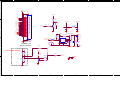
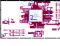
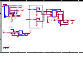
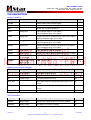
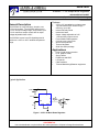
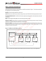
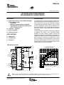
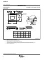
1. Schematic Circuit Diagram
2. Critical Commpoents List
3. IC Date Sheet & IC Description
4. Service Tools and Equipment
Manual
#+,
)
&
!&
&
)
!&
&
$
#
" )!
! "#
&
)
#
'
&&
)
"# )
#+,
&
&
&
&
)
&
&
)
& #
&
! "#
! "#
%
*
%
!&
%
%
$%
!&
(#
)
(#
'
&
)
'
'
'
.
! "#
! "#
! "#
! "#
'
)
&
)
&
&
&&
&)
)
"#
"#
! "#
%
)
&
.
.
-
&
#
#
!
-
" "
#
$% $ "&! %
$ '% (
%
# %
#
#
)
&
!"
$
$
&
)
$#
$
$
! "
#
!
!
!
!
#
#
'
&
$%&
&
&
&
&
&
&
)
)
)&
))
)
)
)
)
)
)
"# )!
)
&
%
!
%
!
#
'
%
#
#
))
! "#
!
&
&
)
)
)
&
#
#
#
)
&
! "#
.
.
#
'
! "#
)
#
! "#
)
&
.
.
%
)
&
)
&
)
! "#
&
&
'
(#
)
)
'
! "#
/
&
! "#
&
'
"#
"#
!
!
)
&
&
! "#
#
)
! "#
)
&
)
! "#
)
#
)&
! "#
#
' &
&"# )!
)
&
)
&
&
)
&
#
#
&
&
&
'
)
&
%
%
)
)
%
%
#
#
#
#
#
#
! "
)
! "
&
! "
))
)& &
&
.
! "#
.
'
(#
(#
&
)
' &
&
)
! "#
.
! "
! "
! "
&
' &
%
1
1
! "#
1
&
(#
(#
&
& &
! "#
&
)
&
! "#
)
!
"#
"#
#$
"
#
! "#
'
)
"# )
)! !
! "#
)
"#
)
&
)
%
)
.
%
&
&
)
.
)
"#
)
%
.
&
! &"#
%
.
(#
(#
)
&
(#
)
%
! !
&
.
,
,
)
&
! &"#
)
.
)
"# )
)! !
)
!
"#
!
"#
) *
*
&
"#
&
)
&
#$
"
2
2
2
#$
&
)
&
)
"# )
)! !
&
"# )
)! !
&
#
)
)
$
#
#
! "#
&"4
(
) *+
*,-./*.0
&
)
#
)
! "#
'
)
&
" )!
)! !
&
)
)
! "#
#
)
$
&
&
! "#
) *
*
%
'
! "#
) *
*
এᥝ
#$
% &'
'
&"
! "#
'
#
"
3
! "#
&
" )!
&
)
&
#$
# )
-
)
+,
&
)! "
%
&
)
54677892 +6:;
'
"
)!
"
)!
%
! "
&
&
!
,#
!
'
&
)
&
! ,
&
1
1
2 2/
& "#
&
#
"# )!
'
)
! "
.
'
&
.
.
.
! "#
&" )!
! "#
)
! "#
$
$
$
$
$
$
$)
$&
&
'
"
&
)
.
)
&
.
)
&
)
&
#
)
&
.
.
)
&
)
&
&
#
#
)*
#
#
"# )!
! !
#
"#
'
#
! "#
,7;,,=
("
<#
#
(#
.#
#
&!)
-
#
"#
! !
(#
#&
&
)*
%
%
("
#
! "#
#
#)
#& ! "#
#
#
%
%
(
#
&#
#
)#
#
#)
! "#
)
)*
&
#
#
#
#
#
#
'
(
#
! "#
#
! "#
#
! "#
<
2<
<
<
)
<
<
<
&
)
<
&
)
&
#
!
!
$&
"
'
!
'
"# )!
&"#
!
>
&"# )!
!
!
! "#
"# )!
'
! "#
&
)?
"#
&
) 8
! "#
#
"# )
)
'
8
) ! "#
"#
$
* ,
,
5$ '
6
5$ ' .
6
.
#-
&"
&
+'
+'
'
+
'
, , -
/
! "#
.
.
'
)
)
! "#
&"# )!
#
#
&
$ !0 0
"- 4"
)
%
(
&
+
(
,
)
'
&
#
-
#
-
! "#
"#
! "#
#
)
)
! "#
! "#
)
)
,#
&
"# )
)
&
#
0&
! .
-
1
!
1.
"
, -
! "#
! "#
)
! "#
&
! "#
! "#
,#
! "#
0&
! .
1 .1 + , 0 2!34 0 "
#
- -!&4 !
7!
"3!
!
"
#
'
( $
$
%
&
$
" % $$
$%
+,$
!
$
$
$
$
)
+
!
*
MST720A/MST720A-A
Small Size LCD TV Processor with Video Decoder
Preliminary Data Sheet Version 0.1
FEATURES
n
n
n
n
Video Decoder
Ÿ Supports NTSC, PAL and SECAM video input
formats
Ÿ 2D NTSC and PAL comb-filter for Y/C
separation of CVBS input
Ÿ Single CVBS and S-video input
Ÿ Supports Closed-caption and V-chip
Ÿ ACC, AGC, and DCGC (Digital Chroma Gain
Control)
Color Engine
Ÿ Brightness, contrast, saturation, and hue
adjustment
Ÿ 9-tap programmable multi-purpose FIR (Finite
Impulse Response) filter
Ÿ Differential 3-band peaking engine
Ÿ Luminance Transient Improvement (LTI)
Ÿ Chrominance Transient Improvement (CTI)
Ÿ Black Level Extension (BLE)
Ÿ White Level Extension (WLE)
Ÿ Favor Color Compensation (FCC)
Ÿ 3-channel gamma curve adjustment
Scaling Engine/TCON
Ÿ Supports analog panels with the resolution of
960x234, 1200x234, 1400x234, and more
Ÿ Supports various displaying modes
Ÿ Supports horizontal panorama scaling
Digital PWM Controller
Ÿ Integrated general purpose digital PWM
control loop
Version 0.1
n
Ÿ Programmable startup operating frequency
and period with output voltage regulation
Ÿ Programmable output current regulation;
40KHz~70KHz switching frequency, sync. to
HSYNC possible
Ÿ Burst-mode or continuous-mode for output
current regulation; 150Hz~300Hz burst-mode
frequency, sync. to VSYNC possible
Ÿ Programmable protection level for input
voltage and fault detection
Miscellaneous
Ÿ Built-in MCU
Ÿ 3-wire serial bus interface for configuration
setup
Ÿ Built-in step-down PWM circuits for input 2.5V
Ÿ Built-in VCOM DC level adjusting circuits
Ÿ Built-in internal OSD with 256 programmable
fonts, 16-color palettes, and 12-bit color
resolution
Ÿ 3-channel low-power 8-bit DAC integration for
RGB output, dynamic range 0.1-4.9V
Ÿ Built-in VCOM DC/AC level adjustment circuit
Ÿ Spread spectrum clocks
Ÿ Optional 3.3V / 5V output pads with
programmable driving current
Ÿ 100-pin LQFP package
-1Copyright © 2005 MStar Semiconductor, Inc. All rights reserved.
11/22/2005
MST720A/MST720A-A
Small Size LCD TV Processor with Video Decoder
Preliminary Data Sheet Version 0.1
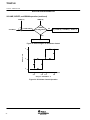
BLOCK DIAGRAM
CVBS
S-Video
SY/CVBS
Switch
SC
2-Channel
AFE
Video Decoder
Timing Generator
YC Separation
2D Comb Filter
3x3 Color Space
Conversion
MACE
Scaling Engine
OSD
Gamma
Display Unit
MCU
BIU
Flash Memory or
EEPROM
Chroma
Demodulator
M
U
X
CSC
(RGB to YCbCr)
TCON
DPWM Controller
Display
Device
DPWM
Output
Feedback Voltage
External MCU
SYSTEM APPLICATION DIAGRAM
Y/CVBS1
C/CVBS2
Version 0.1
Flash / ROM
2.5V
Power Supply
MicroController
PWM
Step-Down
DPWM
Controller
Video
Decoder
TCON
Deinterlacer
/ Scaler
RGB Amplifer
To Analog Panel
-2Copyright © 2005 MStar Semiconductor, Inc. All rights reserved.
11/22/2005
MST720A/MST720A-A
Small Size LCD TV Processor with Video Decoder
Preliminary Data Sheet Version 0.1
GENERAL DESCRIPTION
The MST720A is a high quality ASIC for NTSC/PAL/SECAM car TV application. It receives analog
NTSC/PAL/SECAM CVBS and S-Video inputs from TV tuners, DVD or VCR sources, including weak and distorted
signals. Automatic gain control (AGC) and 8-bit 3-channel A/D converters provide high resolution video
quantization. With automatic video source and mode detection, users can easily switch and adjust variety of
signal sources. Multiple internal adaptive PLLs precisely extract pixel clock from video source and perform
sharp color demodulation. Built-in line-buffer supports adaptive 2-D comb-filter, 2-D sharpening, and
synchronization stabler in a condense manner. The output format of MST720A supports 3.5”~7” analog
TFT-LCD modules.
Version 0.1
-3Copyright © 2005 MStar Semiconductor, Inc. All rights reserved.
11/22/2005
MST720A/MST720A-A
Small Size LCD TV Processor with Video Decoder
Preliminary Data Sheet Version 0.1
76
77
78
79
80
81
82
VR
AVDD_OPLL
GND
GND
VDDC
ROM_EN
INT_OUT
GND
VDDP
83
84
85
86
87
88
89
90
91
92
93
94
95
96
97
98
AVDD_MPLL
GND
HSYNCIN
HSYNCIN
XIN
XOUT
AVDD_DAC
VCOMOUT
VCOMDC
VREP_DAC
VREM_DAC
GND
VB
AVDD_DAC
VG
GND
99
100
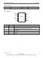
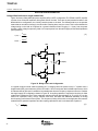
PIN DIAGRAM (MST720A)
GND
VCLAMP
REFM
REFP
AVDD_ADC
1
75
2
74
C1INP
C1INM
YS1INP
YS1INM
CVBS1P
CVBS1M
AVDD_GMC
VIN
FAULTZ
FB2_DPWM
FB1_DPWM
AVDD_SAR
AVSS_SAR
AVSS_DPWM
AVDD_DPWM
Q2
Q1
VDDC
GND
AVDD_PWM
Pin 1
3
73
4
72
5
71
6
70
7
69
8
68
9
67
10
66
11
65
MST720A
XXXXXXXXXXX
XXXXX
12
13
14
15
16
17
64
63
62
61
60
59
50
49
48
47
46
45
44
43
42
41
40
39
38
37
36
35
PWMOUT2
FB2
SENSE2
PWMOUT1
FB1
SENSE1
CP2_FB
CP2_N
CP2_P
CP1_FB
CP1_N
CP1_P
REF_PWM
PGOOD
SAR0
SAR1
SAR2
SCK
SDI
SDO
CSN
PWMD4
INT
SDA
SCL
34
51
33
52
25
32
53
24
31
54
23
30
55
22
29
56
21
28
57
20
27
58
19
26
18
TCON15
TCON14
TCON13
TCON12
TCON11
TCON10
TCON9
TCON8
TCON7
TCON6
TCON5
TCON4
TCON3
TCON2
TCON1
VDDP
GND
GPIO_P01
GPIO_P00
GPIO_P02
RESET
PWMD1
PWMD2
GND
POWER_ON_RSTN/CS
Version 0.1
-4Copyright © 2005 MStar Semiconductor, Inc. All rights reserved.
11/22/2005
MST720A/MST720A-A
Small Size LCD TV Processor with Video Decoder
Preliminary Data Sheet Version 0.1
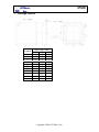
PIN DESCRIPTION
Analog Interface
Pin Name
Pin Type
Function
Pin
VCLAMP
CVBS/YC Mode Clamp Voltage Bypass
2
REFM
Internal ADC Bottom De-coupling Pin
3
REFP
Internal ADC Top De-coupling Pin
4
6
C1INP
Analog Input
Analog Chroma Input for TV S-Video1 /
Analog Composite Input of TV CVBS4
C1INM
Analog Input
Reference Ground for Analog Chroma Input of TV S-Video1 7
/ Analog Composite Input of TV CVBS4
YS1INP
Analog Input
Analog Luma Input of TV S-Video1 /
Analog Composite Input of TV CVBS3
8
YS1INM
Analog Input
Reference Ground for Analog Luma Input of TV S-Video1 /
Analog Composite Input of TV CVBS3
9
CVBS1P
Analog Input
Analog Composite Input for TV CVBS1
10
CVBS1M
Analog Input
Reference Ground for Analog Composite Input of TV CVBS1 11
HSYNCIN
Schmitt Trigger Input
w/ 5V-tolerant
HSYNC / Composite Sync for VGA Input
98
VSYNCIN
Schmitt Trigger Input
w/ 5V-tolerant
VSYNC for VGA Input
97
Analog Panel Output Interface
Pin Name
Pin Type
Function
Pin
VR
Analog Output
Red Channel Output 4.0 Vp-p
84
VG
Analog Output
Green Channel Output 4.0 Vp-p
86
VB
Analog Output
Blue Channel Output 4.0 Vp-p
88
REFM_DAC
DAC Bottom Reference Voltage Decoupling Cap. 1uF to
Ground
90
REFP_DAC
DAC Top Reference Voltage Decoupling Cap. 1uF to
Ground
91
TCON Output
75-61
TCON[15:1]
Output
VCOM Interface
Pin Name
Pin Type
Function
Pin
VCOMDC
Analog Output
Reference DC Voltage Output for Common Amplifier
92
VCOMOUT
Analog Output
Pulse Output for Common Voltage.
93
Version 0.1
-5Copyright © 2005 MStar Semiconductor, Inc. All rights reserved.
11/22/2005
MST720A/MST720A-A
Small Size LCD TV Processor with Video Decoder
Preliminary Data Sheet Version 0.1
Switching Power and PWM Interface
Pin Name
Pin Type
Function
Pin
PWMOUT2
Output
Switching Pulse Output for DC-DC Converter
26
FB2
Analog Input
Error Voltage Feedback Input Pin for PWM2;
voltage = 1.2V
27
SENSE2
Analog Input
Sense Circuit Connection for PWM2
28
PWMOUT1
Output
Switching Pulse Output for DC-DC Converter
29
FB1
Analog Input
Error Voltage Feedback Input Pin for PWM1;
voltage = 1.2V
30
SENSE1
Analog Input
Sense Circuit Connection for PWM1
31
CP2_FB
Analog Input
Error Voltage Feedback Input Pin for CP2; voltage = 1.2V
32
CP2_N
Output
Charge Pump Negative Pulse for DC-DC Negative Voltage
Converter
33
CP2_P
Output
Charge Pump Positive Pulse for DC-DC Negative Voltage
Converter
34
CP1_FB
Analog Input
Error Voltage Feedback Input Pin for CP1; voltage = 1.2V
35
CP1_N
Output
Charge Pump Negative Pulse for DC-DC Positive Voltage
Converter
36
CP1_P
Output
Charge Pump Positive Pulse for DC-DC Positive Voltage
Converter
37
PWM Reference; voltage = 2.4V
38
Power Good Detector
39
REF_PWM
PGOOD
Output
Internal MCU Interface with Serial Flash Memory
Pin Name
Pin Type
Function
Pin
SAR2
Analog Input
SAR Low Speed ADC Input 2
42
SAR1
Analog Input
SAR Low Speed ADC Input 1
41
SAR0
Analog Input
SAR Low Speed ADC Input 0
40
SCK
Output
SPI Interface Sampling Clock
43
SDI
Output
SPI Interface Data-In
44
SDO
Input w/ 5V-tolerant
SPI Interface Data-Out
45
CSN
Output
SPI Interface Chip Select
46
GPIO_P00
I/O w/ 5V-tolerant
General Purpose Input/Output; 4mA driving strength
57
GPIO_P01
I/O w/ 5V-tolerant
General Purpose Input/Output; 4mA driving strength
58
GPIO_P05
I/O w/ 5V-tolerant
General Purpose Input/Output; 4mA driving strength
56
INT
Input
Interrupt Input for IR Receiver
48
SDA
I/O w/ 5V-tolerant
3-Wire Serial Bus Data
49
Version 0.1
-6Copyright © 2005 MStar Semiconductor, Inc. All rights reserved.
11/22/2005
MST720A/MST720A-A
Small Size LCD TV Processor with Video Decoder
Preliminary Data Sheet Version 0.1
Pin Name
Pin Type
Function
Pin
SCL
Input w/ 5V-tolerant
3-Wire Serial Bus Clock
50
POWER_ON_RSTN/CS
Input w/ 5V-tolerant
Power On Reset Signal /
Chip Selection for 3-wire Serial
51
Digital PWM Interface
Pin Name
Pin Type
Function
Pin
Q1
Output
DPWM Output 1
22
Q2
Output
DPWM Output 2
21
FB1_DPWM
Analog Input
st
Input for 1 Feedback Loop
nd
16
FB2_DPWM
Analog Input
Input for 2
Feedback Loop
15
FAULTZ
Analog Input
Fault Detection (Low Enable)
14
VIN
Analog Input
System Input Voltage Detection
13
Misc. Interface
Pin Name
Pin Type
Function
Pin
RESET
Schmitt Trigger Input
w/ 5V-tolerant
Hardware Reset; active high
55
XIN
Analog Input
Crystal Oscillator Input
96
XOUT
Analog Output
Crystal Oscillator Output
95
PWMD4
Output
Pulse Width Modulation Output; 4mA driving strength 47
PWMD2
Output
Pulse Width Modulation Output; 4mA driving strength 53
PWMD1
Output
Pulse Width Modulation Output; 4mA driving strength 54
INT_OUT
Output
Mode Detection Interrupt Output
78
ROM_EN
Input
Internal ROM Enable.
0: Disable.
1: Enable.
79
Power Pins
Pin Name
Pin Type
Function
Pin
AVDD_ADC
2.5V Power
ADC Power
5
AVDD_GMC
5V Power
GMC Power
12
AVDD_SAR
5V Power
SAR Power
17
AVDD_DPWM
5V Power
DPWM Power
20
AVDD_PWM
5V Power
PWM Power
25
AVDD_OPLL
2.5V Power
OPLL Power
83
AVDD_DAC
5V Power
Voltage DAC Power
87, 94
Version 0.1
-7Copyright © 2005 MStar Semiconductor, Inc. All rights reserved.
11/22/2005
MST720A/MST720A-A
Small Size LCD TV Processor with Video Decoder
Preliminary Data Sheet Version 0.1
Pin Name
Pin Type
Function
Pin
AVDD_MPLL
2.5V Power
MPLL Power
100
VDDC
2.5V Power
Digital Core Power
23, 80
VDDP
3.3V/5V Power
Digital Input/Output Power
60, 76
AVSS_SAR
Ground
SAR Ground
18
AVSS_DPWM
Ground
DPWM Ground
19
GND
Ground
Ground
1, 24, 52, 59, 81, 82, 85,
89, 99
Version 0.1
-8Copyright © 2005 MStar Semiconductor, Inc. All rights reserved.
11/22/2005
MST720A/MST720A-A
Small Size LCD TV Processor with Video Decoder
Preliminary Data Sheet Version 0.1
ELECTRICAL SPECIFICATIONS
Absolute Maximum Ratings
Parameter
Symbol
Min
5.0V Supply Voltages
VVDD_50
3.3V Supply Voltages
Typ
Max
Units
-0.3
5.5
V
VVDD_33
-0.3
3.6
V
2.5V Supply Voltages
VVDD_25
-0.3
2.75
V
Input Voltage (5V tolerant inputs)
VIN5Vtol
-0.3
5.0
V
Input Voltage (non 5V tolerant inputs)
VIN
-0.3
VVDD_33
V
Ambient Operating Temperature (commercial use)
TA
0
70
°C
Ambient Operating Temperature (extended temp. range)
TA
-20
80
°C
Storage Temperature
TSTG
-40
125
°C
Junction Temperature
TJ
125
°C
Thermal Resistance (Junction to Air) Natural Conversion
θJA
TBD
°C/W
Thermal Resistance (Junction to Case) Natural Conversion
θJC
TBD
°C/W
Note: Stress above those listed under Absolute Maximum Rating may cause permanent damage to the device. This is a
stress rating only; functional operation of the device at these or any other conditions outside of those indicated in the
operation sections of this specification is not implied. Exposure to absolute maximum ratings for extended periods may
affect device reliability.
ORDERING GUIDE
Model
MARKING INFORMATION
Temperature
Package
Package
Range
Description
Option
MST720A
0°C to +70°C
LQFP
100
MST720A-A
-20°C to +80°C
LQFP
100
MST720A-LF
0°C to +70°C
LQFP
100
MST720A-A-LF
-20°C to +80°C
LQFP
100
MST720A/MST720A-A
Part Number
Lot Number
Operation Code A
Operation Code B
Date Code (YYWW)
Note: Product suffix “-LF” represents lead-free version
and “-A” represents extended temperature range.
DISCLAIMER
MSTAR SEMICONDUCTOR RESERVES THE RIGHT TO MAKE CHANGES WITHOUT FURTHER NOTICE
TO ANY PRODUCTS HEREIN TO IMPROVE RELIABILITY, FUNCTION OR DESIGN.
NO
RESPONSIBILITY IS ASSUMED BY MSTAR SEMICONDUCTOR ARISING OUT OF THE APPLICATION
OR USER OF ANY PRODUCT OR CIRCUIT DESCRIBED HEREIN; NEITHER DOES IT CONVEY ANY
LICENSE UNDER ITS PATENT RIGHTS, NOR THE RIGHTS OF OTHERS.
Electrostatic charges accumulate on both test equipment and human body and can discharge
without detection. MST720A comes with ESD protection circuitry; however, the device may be
permanently damaged when subjected to high energy discharges. The device should be handled
with proper ESD precautions to prevent malfunction and performance degradation.
REVISION HISTORY
Document
Description
Date
MST720A_ds_v01
Ÿ Initial release
Nov 2005
Version 0.1
-9Copyright © 2005 MStar Semiconductor, Inc. All rights reserved.
11/22/2005
MST720A/MST720A-A
Small Size LCD TV Processor with Video Decoder
Preliminary Data Sheet Version 0.1
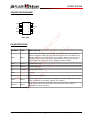
MECHANICAL DIMENSIONS
D
D1
A
A2
A1
θ1
θ2
θ
0.25mm
Seating Plane
θ3
b
L
Version 0.1
c
R1
R2
Gauge Plane
Symbol
L1
S
E2
E1
E
D2
Millimeter
e
Inch
Symbol
Min. Nom. Max. Min. Nom. Max.
Millimeter
Inch
Min. Nom. Max. Min. Nom. Max.
-
0.063
θ
0°
3.5°
7°
0°
3.5°
7°
-
0.006
θ1
0°
-
-
0°
-
-
1.45 0.053 0.055 0.057
θ2
11°
12°
13°
11°
12°
13°
11°
12°
13°
A
-
-
1.60
-
A1
0.05
-
0.15 0.002
A2
1.35
1.40
D
16.00 BSC.
0.630 BSC.
θ3
11°
12°
13°
D1
14.00 BSC.
0.551 BSC.
b
0.17
0.20
0.27 0.007 0.008 0.011
D2
12.00
0.472
c
0.09
-
E
16.00 BSC.
0.630 BSC.
e
E1
14.00 BSC.
0.551 BSC.
L
E2
12.00
0.472
L1
R1
0.08
-
R2
0.08
-
-
0.003
-
-
0.20 0.003
-
0.008
S
0.20 0.004
0.50 BSC.
0.45
0.60
0.008
0.020 BSC.
0.75 0.018 0.024 0.030
1.00 Ref
0.20
-
-
- 10 Copyright © 2005 MStar Semiconductor, Inc. All rights reserved.
0.039 Ref
-
0.008
-
-
11/22/2005
AOZ1041
EZBuck™ 1.5A Simple Buck Regulator
ADVANCED DATASHEET
(Specifications subject to change)
Features
General Description
The AOZ1041 is a high efficiency, simple to use,
1.5A buck regulator. The AOZ1041 works from a
4.5V to 16V input voltage range, and provides up to
1.5A of continuous output current with an output
voltage adjustable down to 0.8V.
The AOZ1041 comes in an SO-8 package and is
rated over a -40°C to +85°C ambient temperature
range.
4.5V to 16V operating input voltage range
130 mΩ internal PFET switch for high
efficiency: up to 95%
Internal Schottky Diode
Internal soft start
Output voltage adjustable to 0.8V
1.5A continuous output current
Fixed 500kHz PWM operation
Cycle-by-cycle current limit
Short-circuit protection
Thermal shutdown
Small size SO-8 package
Applications
Point of load dc/dc conversion
PCIe graphics cards
Set top boxes
DVD drives and HDD
LCD panels
Cable modems
Telecom/Networking/Datacom equipment
Typical Application
Figure 1. 3.3V/1.5A Buck Down Regulator
AOZ1041 Datasheet Rev 0.4
CONFIDENTIAL
Not to be distributed or copied without the written permission of Alpha & Omega Semiconductor
1
Alpha & Omega Semiconductor
AOZ1041
Ordering Information
Part Number
AOZ1041AI
Ambient Temperature Range
-40°C to +85°C
Package
SO-8
Environmental
RoHS Compliant
Pin Configuration
Pin Number
1
2
3
Pin Name
PGND
VIN
AGND
4
FB
5
6
COMP
EN
7,8
LX
8
LX
7
LX
3
6
EN
4
5
COMP
PGND
1
VIN
2
AGND
FB
SO-8
Pin Function
Power ground. Electrically needs to be connected to AGND.
Supply voltage input. When VIN rises above the UVLO threshold the device starts up.
Reference connection for controller section. Also used as thermal connection for
controller section. Electrically needs to be connected to PGND
The FB pin is used to determine the output voltage via a resistor divider between the
output and GND.
External loop compensation pin.
The enable pin is active high. Connect EN pin to VIN if not used. Do not leave the EN
pin floating.
PWM output connection to inductor. Thermal connection for output stage.
AOZ1041 Datasheet Rev 0.4
CONFIDENTIAL
Not to be distributed or copied without the written permission of Alpha & Omega Semiconductor
2
Alpha & Omega Semiconductor
AOZ1041
Absolute Maximum Ratings(1)
Recommend Operating Ratings(2)
Supply Voltage (VIN) ......................................... 18V
LX to AGND.................................-0.7V to VIN+0.3V
EN to AGND ................................-0.3V to VIN+0.3V
FB to AGND...........................................-0.3V to 6V
COMP to AGND ....................................-0.3V to 6V
PGND to AGND................................-0.3V to +0.3V
Junction Temperature (TJ)...........................+150°C
Storage Temperature (TS) ............ -65°C to +150°C
Supply Voltage (VIN)............................. 4.5V to 16V
Output Voltage Range ........................... 0.8V to VIN
Ambient Temperature (TA)..............-40°C to +85°C
Package Thermal Resistance
SO-8 (ΘJA)......................................87°C/W
Electrical Characteristics
TA = 25°C, VIN = VEN = 12V, VOUT = 3.3V unless otherwise specified. Specifications in BOLD indicate a ambient temperature range of -40°C
to +85°C.
Parameter
Supply Voltage
Input under-voltage
lockout threshold
Symbol
VIN
VUVLO
Supply current
(Quiescent)
IIN
Shutdown supply current
IOFF
Feedback Voltage
VFB
Load regulation
Line regulation
Feedback voltage input
current
EN input threshold
EN input hysteresis
Modulator
Frequency
Maximum Duty Cycle
Minimum Duty Cycle
Error amplifier voltage
gain
Error amplifier
transconductance
Protection
Current Limit
Over-temperature
shutdown limit
Soft Start Interval
Output Stage
High-side switch onresistance
Conditions
MIN
4.5
VIN rising
VIN falling
IOUT = 0, VFB = 1.2V,
VEN >1.2V
VEN = 0V
0.782
TYP
MAX
16
4.00
3.70
2
3
UNITS
V
V
V
mA
3
20
µA
0.8
0.818
V
200
%
%
nA
0.5
1
IFB
VEN
Off threshold
On threshold
0.8
V
V
mV
580
500
kHz
%
%
V/V
200
µA/V
2.0
VHYS
100
fO
DMAX
DMIN
380
100
480
6
ILIM
2.0
TJ rising
TJ falling
155
100
4
VIN = 12V
VIN = 5V
97
166
tSS
3.6
A
°C
°C
ms
130
200
mΩ
mΩ
Notes:
1.
2.
3.
Exceeding the Absolute Maximum ratings may damage the device.
The device is not guaranteed to operate beyond the Maximum Operating ratings.
Devices are inherently ESD sensitive, handling precautions are required. Human body model rating: 1.5KΩ in series with 100pF.
AOZ1041 Datasheet Rev 0.4
CONFIDENTIAL
Not to be distributed or copied without the written permission of Alpha & Omega Semiconductor
3
Alpha & Omega Semiconductor
AOZ1041
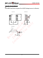
Functional Block Diagram
Vin
UVLO
&
POR
REFERENCE
&
BIAS
0.8V
FB
5V LDO
Internal +5V
REGULATOR
OTP
+
ISEN
SOFTSTART
Q1
ILIMIT
+
+
EAMP
-
PWM
– COMP
PWM
CONTROL
LOGIC
+
LEVEL SHIFTER
+
FET DRIVER
EN
LX
LX
D1
COMP
500Khz
OSCILLATOR
AGND
PGND
AOZ1041 Datasheet Rev 0.4
CONFIDENTIAL
Not to be distributed or copied without the written permission of Alpha & Omega Semiconductor
4
Alpha & Omega Semiconductor
AOZ1041
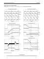
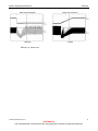
Typical Performance Characteristics
Circuit of figure 1. TA = 25°C, VIN = VEN = 12V, VOUT = 3.3V unless otherwise specified.
Light load (DCM) operation
Full load (CCM) operation
1us/div
1us/div
Start up to full load
Full load to turn off
1ms/div
1ms/div
Load transient
Light load to turn off
100us/div
1s/div
AOZ1041 Datasheet Rev 0.4
CONFIDENTIAL
Not to be distributed or copied without the written permission of Alpha & Omega Semiconductor
5
Alpha & Omega Semiconductor
AOZ1041
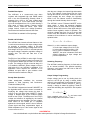
Short circuit protection
Short circuit recovery
100us/div
1ms/div
Efficiency vs. load current
AOZ1041 Datasheet Rev 0.4
CONFIDENTIAL
Not to be distributed or copied without the written permission of Alpha & Omega Semiconductor
6
Alpha & Omega Semiconductor
Detailed Description
The AOZ1041 is a current-mode step down
regulator with integrated high side PMOS switch
and a low side freewheeling Schottky diode. It
operates from a 4.5V to 16V input voltage range
and supplies up to 1.5A of load current. The duty
cycle can be adjusted from 6% to 100% allowing a
wide range of output voltage. Features include
enable control, Power-On Reset, input under
voltage lockout, output over voltage protection,
fixed internal soft-start and thermal shut down.
The AOZ1041 is available in SO-8 package.
AOZ1041
than the error voltage, the internal high-side switch
is on. The inductor current flows from the input
through the inductor to the output. When the current
signal exceeds the error voltage, the high-side
switch is off. The inductor current is freewheeling
through the internal Schottky diode to output.
The AOZ1041 uses a P-Channel MOSFET as the
upper switch. It saves the bootstrap capacitor
normally seen in a circuit which is using an NMOS
switch. It allows 100% turn-on of the upper switch to
achieve linear regulation mode of operation. The
minimum voltage drop from VIN to VO is the load
current times DC resistance of MOSFET plus DC
resistance of buck inductor. It can be calculated by
equation below:
Enable and Soft Start
The AOZ1041 has internal soft start feature to limit
in-rush current and ensure the output voltage ramps
up smoothly to regulation voltage. A soft start
process begins when the input voltage rises to 4.0V
and voltage on EN pin is HIGH. In soft start process,
the output voltage is ramped to regulation voltage in
typically 4ms. The 8ms soft start time is set
internally.
The EN pin of the AOZ1041 is active high. Connect
the EN pin to VIN if enable function is not used. Pull
it to ground will disable the AOZ1041. Do not leave
it open. The voltage on EN pin must rise above 2.0
V to enable the AOZ1041. When voltage on EN pin
falls below 0.8V, the AOZ1041 is disabled. If an
application circuit requires the AOZ1041 to be
disabled, an open drain or open collector circuit
should be used to interface to EN pin.
VO _ MAX = VIN − I O × RDS ( ON )
Where VO_MAX is the maximum output voltage;
VIN is the input voltage from 4.5V to 16V;
IO is the output current from 0A to 1.5A;
RDS(ON) is the on resistance of internal
MOSFET, the value is between 97mΩ and
200mΩ depending on input voltage and
junction temperature;
Switching Frequency
The AOZ1041 switching frequency is fixed and set
by an internal oscillator. The practical switching
frequency could range from 380 kHz to 580 kHz
due to device variation.
Output Voltage Programming
Steady-State Operation
Under steady-state conditions, the converter
operates in fixed frequency and ContinuousConduction Mode (CCM).
The AOZ1041 integrates an internal P-MOSFET as
the high-side switch. Inductor current is sensed by
amplifying the voltage drop across the drain to
source of the high side power MOSFET. Output
voltage is divided down by the external voltage
divider at the FB pin. The difference of the FB pin
voltage and reference is amplified by the internal
transconductance error amplifier. The error voltage,
which shows on the COMP pin, is compared
against the current signal, which is sum of inductor
current signal and ramp compensation signal, at
PWM comparator input. If the current signal is less
Output voltage can be set by feeding back the
output to the FB pin by using a resistor divider
network. In the application circuit shown in Figure 1.
The resistor divider network includes R1 and R2.
Usually, a design is started by picking a fixed R2
value and calculating the required R1 with equation
below.
VO = 0.8 × (1 +
R1
)
R2
Some standard value of R1, R2 and most used
output voltage values are listed in Table 1.
AOZ1041 Datasheet Rev 0.4
CONFIDENTIAL
Not to be distributed or copied without the written permission of Alpha & Omega Semiconductor
7
Alpha & Omega Semiconductor
Table 1.
Vo (V)
R1 (kΩ)
R2 (kΩ)
0.8
1.0
open
1.2
4.99
10
1.5
10
11.5
1.8
12.7
10.2
2.5
21.5
10
3.3
31.1
10
5.0
52.3
10
Combination of R1 and R2 should be large enough
to avoid drawing excessive current from the output,
which will cause power loss.
Since the switch duty cycle can be as high as 100%,
the maximum output voltage can be set as high as
the input voltage minus the voltage drop on upper
PMOS and inductor.
Protection Features
The AOZ1041 has multiple protection features to
prevent system circuit damage under abnormal
conditions.
Over Current Protection (OCP)
The sensed inductor current signal is also used for
over current protection. Since the AOZ1041
employs peak current mode control, the COMP pin
voltage is proportional to the peak inductor current.
The COMP pin voltage is limited to be between
0.4V and 2.5V internally. The peak inductor current
is automatically limited cycle by cycle.
When the output is shorted to ground under fault
conditions, the inductor current decays very slow
during a switching cycle because of Vo=0V. To
prevent catastrophic failure, a secondary current
limit is designed inside the AOZ1041. The
measured inductor current is compared against a
preset voltage which represents the current limit,
between 2.5A and 3.6A. When the output current is
more than current limit, the high side switch will be
turned off and EN pin will be pulled down. The
converter will initiate a soft start once the overcurrent condition disappears.
Power-On Reset (POR)
A power-on reset circuit monitors the input voltage.
When the input voltage exceeds 4V, the converter
starts operation. When input voltage falls below
3.7V, the converter will be shut down.
AOZ1041
Thermal Protection
An internal temperature sensor monitors the
junction temperature. It shuts down the internal
control circuit and high side PMOS if the junction
temperature exceeds 155ºC. The regulator will
restart automatically under the control of soft-start
circuit when the junction temperature decreases to
100ºC.
Application Information
The basic AOZ1041 application circuit is show in
Figure 1. Component selection is explained below.
Input capacitor
The input capacitor must be connected to the VIN
pin and PGND pin of the AOZ1041 to maintain
steady input voltage and filter out the pulsing input
current. The voltage rating of input capacitor must
be greater than maximum input voltage plus ripple
voltage.
The input ripple voltage can be approximated by
equation below:
∆VIN =
IO
V
V
× (1 − O ) × O
f × C IN
VIN
VIN
Since the input current is discontinuous in a buck
converter, the current stress on the input capacitor
is another concern when selecting the capacitor.
For a buck circuit, the RMS value of input capacitor
current can be calculated by:
I CIN _ RMS = I O ×
VO
V
(1 − O )
VIN
VIN
if we let m equal the conversion ratio:
VO
=m
VIN
The relation between the input capacitor RMS
current and voltage conversion ratio is calculated
and shown in Fig. 2 below. It can be seen that when
VO is half of VIN, CIN is under the worst current
stress. The worst current stress on CIN is 0.5·IO.
AOZ1041 Datasheet Rev 0.4
CONFIDENTIAL
Not to be distributed or copied without the written permission of Alpha & Omega Semiconductor
8
Alpha & Omega Semiconductor
AOZ1041
The inductor takes the highest current in a buck
circuit. The conduction loss on inductor need to be
checked for thermal and efficiency requirements.
0.5
0.5
0.4
0.3
I CIN_RMS ( m)
IO
0.2
0.1
0
0
0
0
0.5
m
1
1
Figure 2. ICIN vs. voltage conversion ratio
For reliable operation and best performance, the
input capacitors must have current rating higher
than ICIN-RMS at worst operating conditions. Ceramic
capacitors are preferred for input capacitors
because of their low ESR and high current rating.
Depending on the application circuits, other low
ESR tantalum capacitor may also be used. When
selecting ceramic capacitors, X5R or X7R type
dielectric ceramic capacitors should be used for
their better temperature and voltage characteristics.
Note that the ripple current rating from capacitor
manufactures are based on certain amount of life
time. Further de-rating may be necessary in
practical design.
Inductor
The inductor is used to supply constant current to
output when it is driven by a switching voltage. For
given input and output voltage, inductance and
switching frequency together decide the inductor
ripple current, which is,
∆I L =
VO
V
× (1 − O )
f ×L
VIN
The peak inductor current is:
I Lpeak = I O +
Surface mount inductors in different shape and
styles are available from Coilcraft, Elytone and
Murata. Shielded inductors are small and radiate
less EMI noise. But they cost more than unshielded
inductors. The choice depends on EMI requirement,
price and size.
∆I L
2
High inductance gives low inductor ripple current
but requires larger size inductor to avoid saturation.
Low ripple current reduces inductor core losses. It
also reduces RMS current through inductor and
switches, which results in less conduction loss.
Usually, peak to peak ripple current on inductor is
designed to be 20% to 30% of output current.
When selecting the inductor, make sure it is able to
handle the peak current without saturation even at
the highest operating temperature.
Table below lists some inductors for typical output
voltage design.
Table 2.
Vout L1
5.0 V Unshielded, 4.7uH
LQH55DN4R7M03
Shielded, 4.7uH
LQH66SN4R7M03
Shield, 5.8uH
ET553-5R8
Un-shielded, 4.7uH
DO3316P-472MLD
3.3 V Unshielded, 4.7uH
LQH55DN3R3M03
Shield, 4.7uH
LQH66SN3R3M03
Shield, 3.3uH
ET553-3R3
Un-shielded, 4.7uH
DO3316P-472MLD
Un-shielded, 4.7uH
DO1813P-472HC
1.8 V Unshielded, 2.2uH
LQH55DN1R5M03
Shield, 2.2uH
LQH66SN1R5M03
Shield, 2.2uH
ET553-2R2
Un-shielded, 2.2uH
DO3316P-222MLD
Un-shielded, 2.2uH
DO1813P-222HC
Manufacture
MURATA
MURATA
ELYTONE
Coilcraft
MURATA
MURATA
ELYTONE
Coilcraft
Coilcraft
MURATA
MURATA
ELYTONE
Coilcraft
Coilcraft
Output Capacitor
The output capacitor is selected based on the DC
output voltage rating, output ripple voltage
specification and ripple current rating.
The selected output capacitor must have a higher
rated voltage specification than the maximum
desired output voltage including ripple. De-rating
needs to be considered for long term reliability.
AOZ1041 Datasheet Rev 0.4
CONFIDENTIAL
Not to be distributed or copied without the written permission of Alpha & Omega Semiconductor
9
Alpha & Omega Semiconductor
Output ripple voltage specification is another
important factor for selecting the output capacitor.
In a buck converter circuit, output ripple voltage is
determined by inductor value, switching frequency,
output capacitor value and ESR. It can be
calculated by the equation below:
∆VO = ∆I L × ( ESRCO
1
+
)
8 × f × CO
where CO is output capacitor value and ESRCO is
the Equivalent Series Resistor of output capacitor.
When low ESR ceramic capacitor is used as output
capacitor, the impedance of the capacitor at the
switching frequency dominates. Output ripple is
mainly caused by capacitor value and inductor
ripple current. The output ripple voltage calculation
can be simplified to:
∆VO = ∆I L ×
1
8 × f × CO
If the impedance of ESR at switching frequency
dominates, the output ripple voltage is mainly
decided by capacitor ESR and inductor ripple
current. The output ripple voltage calculation can be
further simplified to:
∆VO = ∆I L × ESRCO
For lower output ripple voltage across the entire
operating temperature range, X5R or X7R dielectric
type of ceramic, or other low ESR tantalum are
recommended to be used as output capacitors.
In a buck converter, output capacitor current is
continuous. The RMS current of output capacitor is
decided by the peak to peak inductor ripple current.
It can be calculated by:
I CO _ RMS =
∆I L
12
Usually, the ripple current rating of the output
capacitor is a smaller issue because of the low
current stress. When the buck inductor is selected
to be very small and inductor ripple current is high,
output capacitor could be overstressed.
Loop Compensation
The AOZ1041 employs peak current mode control
for easy use and fast transient response. Peak
current mode control eliminates the double pole
effect of the output L&C filter. It greatly simplifies
the compensation loop design.
AOZ1041
With peak current mode control, the buck power
stage can be simplified to be a one-pole and onezero system in frequency domain. The pole is
dominant pole can be calculated by:
f P1 =
1
2π × CO × RL
The zero is a ESR zero due to output capacitor and
its ESR. It is can be calculated by:
f Z1 =
1
2π × CO × ESRCO
Where CO is the output filter capacitor;
RL is load resistor value;
ESRCO is the equivalent series resistance
of output capacitor;
The compensation design is actually to shape the
converter control loop transfer function to get
desired gain and phase. Several different types of
compensation network can be used for AOZ1041.
For most cases, a series capacitor and resistor
network connected to the COMP pin sets the polezero and is adequate for a stable high-bandwidth
control loop.
In the AOZ1041, FB pin and COMP pin are the
inverting input and the output of internal
error
amplifier. A series R and C compensation network
connected to COMP provides one pole and one
zero. The pole is:
f P2 =
GEA
2π × CC × GVEA
Where GEA is the error amplifier transconductance,
which is 200·10-6 A/V;
GVEA is the error amplifier voltage gain,
which is 500 V/V;
CC is compensation capacitor;
The zero given by the external compensation
network, capacitor CC and resistor RC, is located at:
fZ2 =
1
2π × CC × RC
To design the compensation circuit, a target
crossover frequency fC for close loop must be
selected. The system crossover frequency is where
control loop has unity gain. The crossover is the
AOZ1041 Datasheet Rev 0.4
CONFIDENTIAL
Not to be distributed or copied without the written permission of Alpha & Omega Semiconductor
10
Alpha & Omega Semiconductor
also called the converter bandwidth. Generally a
higher bandwidth means faster response to load
transient. However, the bandwidth should not be
too high because of system stability concern. When
designing the compensation loop, converter stability
under all line and load condition must be
considered.
Usually, it is recommended to set the bandwidth to
be equal or less than 1/10 of switching frequency.
The AOZ1041 operates at a fixed 500kHz switching
frequency. It is recommended to choose a
crossover frequency equal or less than 50kHz.
f C = 50kHz
The strategy for choosing RC and CC is to set the
cross over frequency with RC and set the
compensator zero with CC. Using selected
crossover frequency, fC, to calculate RC:
RC = f C ×
VO
2π × CO
×
VFB GEA × GCS
where fC is desired crossover frequency. For best
performance, fc is set to be about 1/10 of
switching frequency;
VFB is 0.8V;
GEA is the error amplifier transconductance,
which is 200·10-6 A/V;
GCS is the current sense circuit
transconductance, which is 6.68 A/V;
The compensation capacitor CC and resistor RC
together make a zero. This zero is put somewhere
close to the dominate pole fp1 but lower than 1/5 of
selected crossover frequency. CC can is selected by:
1.5
CC =
2π × RC × f P1
Equation above can also be simplified to:
C × RL
CC = O
RC
An easy-to-use application software which helps to
design and simulate the compensation loop can be
found at www.aosmd.com.
AOZ1041
Thermal management and layout consideration
In the AOZ1041 buck regulator circuit, high pulsing
current flows through two circuit loops. The first
loop starts from the input capacitors, to the VIN pin,
to the LX pins, to the filter inductor, to the output
capacitor and load, and then return to the input
capacitor through ground. Current flows in the first
loop when the high side switch is on. The second
loop starts from inductor, to the output capacitors
and load, to the PGND pin of the AOZ1041, to the
LX pins of the AOZ1041. Current flows in the
second loop when the low side diode is on.
In PCB layout, minimizing the two loops area
reduces the noise of this circuit and improves
efficiency. A ground plane is strongly recommended
to connect input capacitor, output capacitor, and
PGND pin of the AOZ1041.
In the AOZ1041 buck regulator circuit, the two
major power dissipating components are the
AOZ141 and output inductor. The total power
dissipation of converter circuit can be measured by
input power minus output power.
Ptotal = VIN ⋅ I IN − VO ⋅ I O
The power dissipation of inductor can be
approximately calculated by output current and
DCR of inductor.
Pindcutor = I O ⋅ Rinductor ⋅ 1.1
2
The actual junction temperature can be calculated
with power dissipation in the AOZ1041 and thermal
impedance from junction to ambient.
T junction = ( Ptotal − Pinductor ) ⋅ Θ JA
The maximum junction temperature of AOZ1041 is
150ºC, which limits the maximum load current
capability. Please see the thermal de-rating curves
for the maximum load current of the AOZ1041
under different ambient temperature.
The thermal performance of the AOZ1041 is
strongly affected by the PCB layout. Extra care
should be taken by users during design to ensure
that the IC will operate under the recommended
environmental conditions.
Several layout tips are listed below for the best
electric and thermal performance:
1. Do not use thermal relief connection to the VIN
and the PGND pin. Pour a maximized copper
AOZ1041 Datasheet Rev 0.4
CONFIDENTIAL
Not to be distributed or copied without the written permission of Alpha & Omega Semiconductor
11
Alpha & Omega Semiconductor
2.
3.
4.
5.
6.
7.
AOZ1041
area to the PGND pin and the VIN pin to help
thermal dissipation.
Input capacitor should be connected to the VIN
pin and the PGND pin as close as possible.
A ground plane is preferred. If a ground plane
is not used, separate PGND from AGND and
connect them only at one point to avoid the
PGND pin noise coupling to the AGND pin.
Make the current trace from LX pins to L to Co
to the PGND as short as possible.
Pour copper plane on all unused board area
and connect it to stable DC nodes, like VIN,
PGND or SGND.
Keep sensitive signal trace away from
switching node, LX. The copper pour area
connected to the LX pin should be as small as
possible to avoid the switching noise on the LX
pin coupling to other part of circuit.
The AOZ1041-EVA document provides an
example of proper layout techniques.
AOZ1041 Datasheet Rev 0.4
CONFIDENTIAL
Not to be distributed or copied without the written permission of Alpha & Omega Semiconductor
12
Monolithic Digital Stereo FM Transmitter
Radio-Station-on-a-Chip™
KT0801
Xtal1
Features
Professional Grade System-on-a-Chip (SoC) HighFidelity Stereo Audio FM Transmitter:
SNR ≥ 68 dB
Stereo Separation > 50dB
International compatible 76MHz ~ 108MHz
Minimal External Component Requirement:
Crystal optional (in lieu of direct feeding
of an external clock)
Ultra-Low Power Consumption:
< 12.6 mA operation current
< 1 µA standby current
Dual Reference Clock Setup:
Supports both 7.6MHz and 15.2MHz
Small Form factor:
24-pin 4x4x0.9 mm QFN (Pb-free and
RoHS Compliant)
Simple Interface:
Single 1.8V (in lieu of 1.6~3.6V regulator
feed)
2
Industry standard 2-wire I C MCU
interface compatible
Advanced Digital Audio Signal Processing:
On-chip 20-bit ∆Σ Audio ADC
On-chip DSP core
On-chip 24dB PGA
Automatic calibration against process
and temperature
On-Chip LDO (low-drop-out) regulator:
Accommodates 1.6V ~ 3.6V supply
Programmable transmit level
Programmable pre-emphasis (50/75 µs)
Applications
MP3 Players
Cellular Phones
PDAs
Portable Personal Media player
Laptop Computers
Wireless Speakers
Xtal2
KTAT0801 Block Diagram
XTAL
Left In
PGA/ADC
Pre-Emph
Digital MPX
Right In
PGA/ADC
SDA
SCL
I2C
KTM proprietary
Frequency Synthesizer
& FM modulator
Pre-Emph
Channel
Selector
Control
Register
Bandgap &
Reference
RF
Power
Amp
Calibration
RF Out
Figure 1: KT0801 System Diagram
General Description
The KT Micro KT0801 Monolithic Digital FM Transmitter
is designed to process high-fidelity stereo audio signal and
transmit modulated FM signal over a short range. The
modulated stereo FM signal can be intercepted and played
back using any FM radio worldwide.
The KT0801 features dual 20-bit ΔΣ audio ADCs, a highfidelity digital stereo audio processor and a fully integrated
radio frequency (RF) transmitter. An on-chip low-drop-out
regulator (LDO) allows the chip to be integrated in a wide
range of low-voltage battery-operated systems with power
supply ranging from 1.6V to 3.6V.
The KT0801 is configured as an I2C slave and programmed
through the industry standard 2-wire MCU interface.
Thanks to its high integration level, the KT0801 is mounted
in a generic 24-pin 4x4 QFN package and only requires a
single low-voltage supply and a small-form-factor crystal
(7.6MHz or 15.2MHz) or an external clock to operate.
No external tuning is required that makes design-in effort
minimum.
Rev. 1.1
Information furnished by KT Micro is believed to be accurate
and reliable. However, no responsibility is assumed by KT
Micro for its use, nor for any infringements of patents or
other rights of third parties which may result from its use. No
license is granted by implication or otherwise under any
patent or patent rights of KT Micro.
KT Micro Inc., 22391 Gilberto, Suite D
Rancho Santa Margarita, CA 92688
Tel: 949.713.4000
www.ktmicro.com
Fax: 949.713.404
Copyright ©2006, KT Micro Inc.
KT0801
Operation Condition
Table 1: Operation Condition
Parameter
Symbol
Operating Condition
Min
Typ
1.8V Analog Supply1 VDD
Relative to GND
1.6
1.8
IO/Regulator Supply IOVDD
Relative to GND
1.6
Operating Temp
TA
Ambient Temperature
-30
25
Note: 1. When LDO enabled, no external voltage should be applied to this 1.8V supply.
Max
2.0
3.6
85
Units
V
V
°C
Specifications and Features
Table 2: FM Transmitter Functional Parameters (Unless otherwise noted TA = -30~85 oC,
IOVDD=1.6~3.6 V with LDO enabled, Fin = 1 kHz)
Parameter
Symbol Test/Operating
Min
Nom
Condition
FM Frequency Range
Ftx
Pin 19
76
Current Consumption
IVDD
Pin 1 with PA (power
10
amp.) at default power
mode
Standby Current
Istand
Pin 1
0.1
Signal to Noise Ratio
SNR
Vin = 0.7 Vp-p, Gin = 0
68
Total Harmonic Distortion
THD
Vin = 0.7 Vp-p, Gin = 0
0.1
Left/Right Channel Balance
BAL
Vin = 0.7 Vp-p, Gin = 0
-0.2
Stereo Separation (Left<->Right) SEP
Vin = 0.7 Vp-p, Gin = 0
50
60
Sub Carrier Rejection Ratio
SCR
Vin = 0.7 Vp-p, Gin = 0
Input Swing1
Vin
Single-ended input
0.3
PGA Range for Audio Input
Gin
-12
0
PGA Gain Step for Audio Input
Gstep
4
Required Input Common-Mode
Vcm
Pin 4, 6
0
0.8
Voltage when DC-coupled
Power Supply Rejection2
PSRR
IOVDD = 1.9 ~ 3.6 V
40
Ground Bounce Rejection2
GSRR
IOVDD = 1.9 ~ 3.6 V
40
Input Resistance (Audio Input)
Rin
Pin 4, 6
120
150
Input Capacitance (Audio Input) Cin
Pin 4, 6
0.5
0.8
Audio Input Frequency Band
Fin
Pin 4, 6
20
Transmit Level
Vout
Spectrum analyzer (50
93
99
Ω)
Channel Step
STEP
100
Pre-emphasis Time Constant
Tpre
SIG_PROC<1> = 1
50
SIG_PROC<0> = 0
75
Crystal/External Clock
CLK
Dual-frequency setup
7.6 or
15.2
2-wire I2C Clock
SCL
Pin 17
0
100
High Level Input Voltage
VIH
Pin 3, 9, 10, 12, 13, 16,
0.75 x
17, 24
IOVDD
Low Level Input Voltage
VIL
Pin 3, 9, 10, 12, 13, 16,
- 0.25
17, 24
Notes:
1. Maximum is given on the condition of PGA gain = -12dB.
2. Fin = 20 ~ 15k Hz.
Copyright ©2006, KT Micro, Inc.
Max
Units
108
MHz
12.6
mA
1
-
μA
dB
%
dB
dB
dB
VRMS
dB
dB
0.2
-60
1.2
12
1.8
V
180
1.2
15k
dB
dB
kΩ
pF
Hz
104
dBµV
-
kHz
µs
µs
-
MHz
400
IOVDD
+ 0.25
0.25 x
IOVDD
kHz
V
V
KT0801
Package and Pin List
A 24-pin QFN package is used. The chip IO pin-out is listed in Table 3.
Table 3 KT0801 Pin-Out
Pin Index Name
1
IOVDD
2, 14, 18, VDD
22
3
HF
4
5, 11, 15,
20, 21
6
7
8
9
10
12
13
16
17
19
23
24
I/O Type
Power
Power
INL
GND
Analog Input
Ground
Function
1.6~3.3V external logic IOVDD or Regulator high supply input.
1.8V supply. No external voltage shall be applied with regulator
enabled. All four pins shall be shorted on the PCB.
“1” to enable 15.2MHz XTAL mode. Default “0”, 7.6MHz
XTAL mode.
Left channel audio input.
Ground.
INR
NC1
NC2
SW1
SW2
RSTB
ADDR
SDA
SCL
PA_OUT
XI
XO/RCLK
Analog Input
N/A
N/A
Digital Input
Digital Input
Digital Input
Digital Input
Digital I/O
Digital I/O
Analog Output
Analog I/O
Analog I/O
Right channel audio input.
Reserved. Do not connect.
Reserved. Do not connect.
Control bit. Chip enable, supply mode and clock source.
Control bit. Chip enable, supply mode and clock source.
Reset (active low).
Set the 4th I2C address bit (MSB being the 1st bit).
Serial data I/O.
Serial clock input.
FM RF output.
Crystal input.
Crystal input or external reference clock input.
Digital Input
Copyright ©2006, KT Micro, Inc.
KT0801
XO/CLK
XI
VDD
GND
GND
PA_OUT
24
23
22
21
20
19
IOVDD
VDD
HF
INL
GND
INR
1
18
2
17
3
16
Top View
4
15
5
14
6
13
VDD
SCL
SDA
GND
VDD
ADDR
7
8
9
10
11
12
NC1
NC2
SW1
SW2
GND
RSTB
Figure 2: KT0801 Pin-out: 4x4 24-Pin QFN Package.
Copyright ©2006, KT Micro, Inc.
KT0801
I2C Compatible 2-Wire Serial Interface
General Descriptions
The serial interface consists of a serial controller and registers. An internal address decoder transfers the
content of the data into appropriate registers. Both the write and read operations are supported according to
the following protocol:
The write operation is accomplished via a 3-byte sequence:
Serial address with write command
Register address
Register data
The read operation is accomplished via a 4-byte sequence:
Serial address with write command
Register address
Serial address with read command
Register data
RANDOM REGISTER WRITE PROCEDURE
S 0 1 1 x 1 1 0 WA
7 bit address
START condition
A
register address
Acknowledge
WRITE command
AP
data
Acknowledge
STOP condition
Acknowledge
RANDOM REGISTER READ PROCEDURE
S 0 1 1 x 1 1 0 WA
7 bit address
START condition
register address
Acknowledge
WRITE command
AS 0 1 1 x 1 1 0 R A
7 bit address
Acknowledge
AP
data
Acknowledge
READ condition
NO Acknowledge
STOP condition
Figure 3: Serial Interface Protocol
th
The x is the optional 4 MSB bit address code that is set by the ADDR pin and is provided to allow a dualtransmitter-single-controller configuration that will enable multi-channel surround sound applications.
ADDR must be externally tied to ground or IOVDD for low or high setup, respectively. The serial
controller supports slave mode only. Any register can be addressed randomly.
Slave Mode Protocol
With reference to the clocking scheme shown in Figure 4, the serial interface operates in the following
manner:
Copyright ©2006, KT Micro, Inc.
KT0801
8-bit
8-bit
Slave Address & R/W
DATA
Acknowledge
Start
Condtion
Acknowledge
Stop
Condtion
Figure 4: Serial Interface Slave Mode Protocol
A START condition is defined as a HIGH to LOW transition on the data line while the SCLK line is held
high. After this has been transmitted by the controller (Master), the bus is considered busy. The next byte of
data transmitted after the start condition contains the address of the slave in the first 7 bits and the 8th bit
tells whether the master is receiving data from the slave or transmitting data to the slave. When ADDR is
set to “0” (i.e. tied to ground), the I2C write address is 0x6C and the read address is 0x6D.
Data transfer with acknowledge is obligatory. The transmitter must release the SDA line during the
acknowledge pulse. The receiver must then pull the SDA line LOW so that it remains stable during the
HIGH period of the acknowledge clock pulse. A receiver that has been addressed is obligated to generate
an acknowledge signal after each byte of data has been received.
Register Bank
The register bank stores channel frequency codes, calibration parameters, operation status, mode and power
controls, which can be accessed by the internal digital controller, state machines and external micro
controllers through the serial interface.
All registers are 8 bits wide. Control logics are active high unless specifically noted.
CH_SEL0 (Address: 0x00, Default: 0x81)
Bits
Type
Default
Label
Description
FM Channel Selection[7:0]
7:0
RW
0x81
CHSEL[7:0]
CHSEL[10:0] definition : Channel selection code. 0 to 108 MHz with 100 kHz step. 0x000 corresponds to
0Hz; 0x001 corresponds to 100 kHz, and so on.
CH_SEL1 (Address: 0x01, Default: 0x03)
Bits
7:6
Type
RW
Default
0x0
Label
RFGAIN[1:0]
Description
Transmission Range Adjust
00: Lowest Range
01: Low Range
10: High Range
11: Highest Range
Copyright ©2006, KT Micro, Inc.
KT0801
Bits
5:3
Type
RW
Default
0x0
Label
PGA[2:0]
2:0
RW
0x3
CHSEL[10:8]
Description
Input Audio Gain Control
111: 12dB
110: 8dB
101: 4dB
100: 0dB
000: 0dB
001: -4dB
010: -8dB
011: -12dB
FM Channel Selection[10:8]
SIG_PROC (Address: 0x02, Default: 0x00)
Bits
7:4
3
Type
RW
RW
Default
0x0
0
Label
NA
MUTE
2
RW
0
PLTADJ
1
0
RW
RW
0
0
NA
PHTCNST
Description
Reserved
Software control of Mute
1: MUTE Enable
0: MUTE Disable
Pilot Tone Amplitude Adjustment
1: Amplitude high
0: Amplitude low
Reserved
Pre-Emphasis Time-Constant Set
1: 50uS (Europe, Australia)
0: 75uS (USA, Japan)
PA_PWR (Address: 0x13, Default: 0x00)
Bits
7
Type
RW
Default
0
Label
PA_HI_PW
6:0
RW
0x0
NA
Description
PA (Power amplifier) power (combined with
CH_SEL1<7:6> to set up transmission range)
1: Enable high power
0: Disable high power
Reserved
Chip Enable and Mode Control (Pin 9 and 10)
There are 2 external Pins SW1 and SW2 (Pin 9 and 10) which enable chip and define the supply voltage
level and clock source of the chip. The definition is shown in Table 4.
Table 4: Pin SW1 and SW2 vs. Chip Supply and Clock Source
Input
Chip Mode
Chip Supply
Clock
Source
Disabled
Bypass XTAL
LDO Disabled
LDO Enabled
N/A
Lo-V (1.6~2.0V)
Lo-V (1.6~2.0V)
Hi-V (1.6~3.6V)
External
External
XTAL
XTAL
SW1/2
00
01
10
11
Application note 1: In low supply mode (1.6 ~ 2.0V) and operate with LDO disabled, tie SW2 to ground
and use SW1 as the chip enable. For high supply mode and operate with LDO enabled, short SW2 to SW1
and use both as chip enable.
Copyright ©2006, KT Micro, Inc.
KT0801
Application note 2: In low supply mode, IOVDD (Pin 1) shall be tied to the system supply which is equal
to the logic level “High” from the MCU/system.
Typical Application Circuits
The KTAT08001 can be integrated in a wide range of systems by requiring only a single power supply.
Figure 5 shows a configuration with zero external components. Figure 6 and Figure 7 show two typical
configurations in 1.8V and 3.3Vsystems, respectively.
MCU
(1.8V CMOS Logic)
I 2C
SDA SCL
POR
On/Off
RSTB
SW1 SW2
INL
Stereo Audio
Line Input
Antenna
PA_OUT
KT0801
INR
HF
Other
VDDs IOVDD GND
1.8V
XI
XO
7.6MHz
Clock
Figure 5: Zero external components configuration in 1.8V systems.
Copyright ©2006, KT Micro, Inc.
KT0801
MCU
(1.8V CMOS Logic)
I 2C
POR
On/Off
Optional
SDA SCL
33nF
SW1 SW2
RSTB
INL
Stereo Audio
Line Input
Antenna
PA_OUT
KT0801
INR
33nF
HF
Other
VDDs IOVDD GND
1.8V
XI
XO
7.6MHz
XTAL
15pF
15pF
Figure 6: Typical Application configuration in 1.8V systems.
MCU
(3.3V CMOS Logic)
I 2C
Optional
SDA SCL
33nF
POR
On/Off
RSTB
Antenna
SW1 SW2
INL
PA_OUT
Stereo Audio
Line Input
KT0801
INR
HF
33nF
Other
VDDs
0.1uF
IOVDD GND
XI
3.3V
15pF
XO
15.2MHz
XTAL
15pF
Figure 7: Typical Application configuration in 3.3V system.
Copyright ©2006, KT Micro, Inc.
KT0801
Package Outline
Symbols
A
A1
b
C
D
D2
E
E2
e
L
y
(MILLIMETERS)
MIN NOM MAX
0.80
0.85
0.90
0.00
0.02
0.05
0.20
0.25
0.30
0.19
0.20
0.25
3.95
4.00
4.05
2.65
2.70
2.75
3.95
4.00
4.05
2.65
2.70
2.75
0.5
0.30
0.40
0.50
0.00
0.076
Copyright ©2006, KT Micro, Inc.
PS25LV512 / PS25LV010
512 Kbit / 1 Mbit 3.0 Volt-only, Serial Flash Memory
With 33 MHz SPI Bus Interface
FEATURES
Block Write Protection
- The Block Protect (BP1, BP0) bits allow part or entire
of the memory to be configured as read-only.
Single Power Supply Operation
- Voltage range: 3.0V - 3.6V
• Memory Organization
- PS25LV512: 64K x 8 (512 Kbit)
- PS25LV010: 128K x 8 (1 Mbit)
Hardware Data Protection
- Write Protect (WP#) pin will inhibit write operations
to the status register
Cost Effective Sector/Block Architecture
- Uniform 4 Kbyte sectors
- Uniform 32 Kbyte blocks (8 sectors per block)
- Two blocks with 32 Kbytes each (512 Kbit)
- Four blocks with 32 Kbytes each (1 Mbit)
- 128 pages per block
Ms
ta
In fo r
te r Co
rn Ho nf
al ne id
e
s
Us ta nt
e r ia
l
On
ly
• Page Program (up to 256 Bytes)
- Typical 3 ms per page program time
• Sector, Block and Chip Erase
- Typical 60 ms sector/block/chip erase time
Single Cycle Reprogramming for Status Register
- Build-in erase before programming
Serial Peripheral Interface (SPI) Compatible
- Supports SPI Modes 0 (0,0) and 3 (1,1)
High Product Endurance
- Guarantee 10,000 program/erase cycles per single
sector
- Minimum 10 years data retention
High Performance Read
- 33MHz clock rate (max) for NORMAL READ
- 33MHz clock rate (max) for FAST READ
Page Mode for Program Operations
- 256 bytes per page
Industrial Standard Pin-out and Package
- 8-pin JEDEC SOIC
- Optional lead-free (Pb-free) packages
GENERAL DESCRIPTION
The PS25LV512/010 are 512 Kbit/1 Mbits 3.0 Volt-only serial Flash memories. These devices are designed to use
a single low voltage, range from 3.0 Volt to 3.6 Volt, power supply to perform read, erase and program operations.
The devices can be programmed in standard EPROM programmers as well.
The device is optimized for use in many commercial applications where low-power and low-voltage operation are
essential. The PS25LV512/010 is enabled through the Chip Enable pin (CE#) and accessed via a 3-wire interface
consisting of Serial Data Input (Sl), Serial Data Output (SO), and Serial Clock (SCK). All write cycles are completely self-timed.
Block Write protection for top 1/4, top 1/2 or the entire memory array (1M) or entire memory array (512K) is enabled
by programming the status register. Separate write enable and write disable instructions are provided for additional
data protection. Hardware data protection is provided via the WP pin to protect against inadvertent write attempts
to the status register. The HOLD pin may be used to suspend any serial communication without resetting the serial
sequence.
Programmable Microelectronics Corp.
1
Issue Date: September, 2005, Rev: 1.0
PS25LV512/010
CONNECTION DIAGRAMS
1
8
Vcc
SO
2
7
HOLD#
WP#
3
6
SCK
GND
4
5
SI
Ms
ta
In fo r
te r Co
rn Ho nf
al ne id
e
s
Us ta nt
e r ia
l
On
ly
CE#
8-Pin SOIC
PIN DESCRIPTIONS
S YMB OL
T YP E
D E S C R IP T ION
CE#
INP UT
C hip E nable: C E # goes low activates the device's internal circuitries for
device operation. C E # goes high deselects the device and switches into
standby m ode to reduce the power consumption. W hen the device is not
selected, data will not be accepted via the serial input pin (S l), and the
serial output pin (S O) will remain in a high im pedance state.
SCK
INP UT
S erial D ata C lock
SI
INP UT
S erial D ata Input
SO
OUTP UT
S erial D ata Output
GND
Ground
V cc
D evice P ower S upply
WP#
INP UT
W rite P rotect: W hen the W P # pin brought to low and W P E N bit is "1", all
write operations to the status register are inhibited.
HOLD #
INP UT
Hold: P ause serial communication with the master device without
resetting the serial sequence.
Programmable Microelectronics Corp.
2
Issue Date: September, 2005, Rev: 1.0
PS25LV512/010
PRODUCT ORDERING INFORMATION
PS25LVxxx
-33
S
C
E
Environmental Attribute
E = Lead-free (Pb-free) Package
Blank = Standard Package
Temperature Range
C = Commercial (0°C to +85°C)
Ms
ta
In fo r
te r Co
rn Ho nf
al ne id
e
s
Us ta nt
e r ia
l
On
ly
Package Type
S = 8-pin SOIC (8S)
Operating Speed
-33 : 33MHz (max) for Normal and Fast read
Products Device Number
PS25LV512 (512 Kbit)
PS25LV010 (1 Mbit)
Part Number
Operating Frequency (MHz)
Package
Temperature Range
33
8S
Commercial
o
o
(0 C to + 85 C)
PS25LV512-33SC
PS25LV512-33SCE
PS25LV010-33SC
PS25LV010-33SCE
Programmable Microelectronics Corp.
3
Issue Date: September, 2005, Rev: 1.0
PS25LV512/010
BLOCK DIAGRAM
SPI Chip Block Diagram
High Voltage
Generator
Control Logic
Ms
ta
In fo r
te r Co
rn Ho nf
al ne id
e
s
Us ta nt
e r ia
l
On
ly
Instruction Decoder
Serial /Parallel convert Logic
Y-DECODER
Address Latch
& Counter
2KBit Page Buffer
Status
Register
Memory Array
X-DECODER
Programmable Microelectronics Corp.
4
Issue Date: September, 2005, Rev: 1.0
PS25LV512/010
SERIAL INTERFACE DESCRIPTION
PS25LV512/010 can be driven by a microcontroller on the SPI bus as shown in Figure 1. The serial communication
term definitions are in the following section.
MASTER: The device that generates the serial clock.
SLAVE: Because the Serial Clock pin (SCK) is always an input, the PS25LV512/010 always operates as a slave.
Ms
ta
In fo r
te r Co
rn Ho nf
al ne id
e
s
Us ta nt
e r ia
l
On
ly
TRANSMITTER/RECEIVER: The PS25LV512/010 has separate pins designated for data transmission (SO) and
reception (Sl).
MSB: The Most Significant Bit (MSB) is the first bit transmitted and received.
SERIAL OP-CODE: After the device is selected with CE# going low, the first byte will be received. This byte
contains the op-code that defines the operations to be performed.
INVALID OP-CODE: If an invalid op-code is received, no data will be shifted into the PS25LV512/010, and the serial
output pin (SO) will remain in a high impedance state until the falling edge of CE# is detected again. This will
reinitialize the serial communication.
Figure 1. Bus Master and SPI Memory Devices
SDO
SPI Interface with
(0, 0) or (1, 1)
SDI
SCK
SCK
SO
SCK SO
SI
SI
SCK
SO
SI
Bus Master
SPI Memory
Device
CS3
SPI Memory
Device
SPI Memory
Device
CS2 CS1
CE#
WP# HOLD# CE#
WP# HOLD# CE#
WP# HOLD#
Note: 1. The Write Protect (WP#) and Hold (HOLD#) si gnals should be driven, High or Low as appropriate.
Programmable Microelectronics Corp.
5
Issue Date: September, 2005, Rev: 1.0
PS25LV512/010
SERIAL INTERFACE DESCRIPTION (CONTINUED)
SPI MODES
available from the falling edge of Serial Clock (SCK).
These devices can be driven by microcontroller with its
SPI peripheral running in either of the two following modes:
Mode 0 = (0, 0)
Mode 3 = (1, 1)
Ms
ta
In fo r
te r Co
rn Ho nf
al ne id
e
s
Us ta nt
e r ia
l
On
ly
For these two modes, input data is latched in on the
rising edge of Serial Clock (SCK), and output data is
The difference between the two modes, as shown in
Figure 2, is the clock polarity when the bus master is in
Stand-by mode and not transfering data:
- Clock remains at 0 (SCK = 0) for Mode 0 (0, 0)
- Clock remains at 1 (SCK = 1) for Mode 3 (1, 1)
Figure 2. SPI Modes
Mode 0 (0
0) S C K
Mode 3 (1
1) S C K
SI
SO
Programmable Microelectronics Corp.
6
Issue Date: September, 2005, Rev: 1.0
PS25LV512/010
DEVICE OPERATION
The PS25LV512/010 is designed to interface directly with the synchronous serial peripheral interface (SPI) of the
6800 type series of microcontrollers.
The PS25LV512/010 utilizes an 8-bit instruction register. The list of instructions and their operation codes are
contained in Table 1. All instructions, addresses, and data are transferred with the MSB first and start with a highto-low transition.
Write is defined as program and/or erase in this specification. The following commands, PAGE PROGRAM,
SECTOR ERASE, BLOCK ERASE, CHIP ERASE, and WRSR are write instructions for PS25LV512/010.
Ms
ta
In fo r
te r Co
rn Ho nf
al ne id
e
s
Us ta nt
e r ia
l
On
ly
Table 1. Instruction Set for the PS25LV512/010
Instruction N ame
Instruction Format
H ex C ode
Operation
WREN
0000 0110
06h
Set Write Enable Latch
WRD I
0000 0100
04h
Reset Write Enable Latch
RDSR
0000 0101
05h
Read Status register
WRSR
0000 0001
01h
Write Status Register
READ
0000 0011
03h
Read Data from Memory Arrary
FAST_READ
0000 1011
0Bh
Read Data from Memory at Higher Speed
PG_ PROG
0000 0010
02h
Program D ata Into Memory Array
SEC TOR_ERASE
1101 0111
D 7h
Erase One Sector in Memory Array
BLOC K_ERASE
1101 1000
D 8h
Erase One Block in Memory Array
C HIP_ERASE
1100 0111
C 7h
Erase Entire Memory Array
RDID
1010 1011
ABh
Read Manufacturer and Product ID
READ PRODUCT ID (RDID): The RDID instruction allows the user to read the manufacturer and product ID of the
device. The instruction code is followed by three dummy bytes, each bit being latched-in on Serial Data Input (SI)
during the rising edge of Serial Clock (SCK). Then the first manufacturer ID (9Dh) is shifted out on Serial Data
Output (SO), followed by the device ID (7Bh = PS25LV512; 7Ch = PS25LV010) and the second manufacturer ID
(7Fh), each bit been shifted out during the falling edge of Serial Clock (SCK).
Table 2. Product Identification
Product Identification
Data
Manufacturer ID
9Dh
Device ID:
PS25LV512
7Bh
PS25LV010
7Ch
Programmable Microelectronics Corp.
7
Issue Date: September, 2005, Rev: 1.0
PS25LV512/010
WRITE ENABLE (WREN): The device will power up in the write disable state when Vcc is applied. All write
instructions must therefore be preceded by the WREN instruction.
WRITE DISABLE (WRDI): To protect the device against inadvertent writes, the WRDI instruction disables all write
commands. The WRDI instruction is independent of the status of the WP# pin.
READ STATUS REGISTER (RDSR): The RDSR instruction provides access to the status register. The READY/
BUSY and write enable status of the device can be determined by the RDSR instruction. Similarly, the Block Write
Protection bits indicate the extent of protection employed. These bits are set by using the WRSR instruction.
During internal write cycles, all other commands will be ignored except the RDSR instruction.
Ms
ta
In fo r
te r Co
rn Ho nf
al ne id
e
s
Us ta nt
e r ia
l
On
ly
Table 3. Status Register Format
Bit 7
Bit 6
Bit 5
Bit 4
Bit 3
Bit 2
Bit 1
Bit 0
WPEN
X
X
X
BP1
BP0
WEN
RDY
Table 4. Read Status Register Bit Definition
Bit
Definition
Bit 0 (RDY)
Bit 0 = 0 indicates the device is READY.
Bit 0 = 1 indicates the write cycle is in progress and the device is
BUSY.
Bit 1 (WEN)
Bit 1 = 0 indicates the device is not WRITE ENABLED.
Bit 1 = 1 indicates the device is WRITE ENABLED.
Bit 2 (BP0)
See Table 5.
Bit 3 (BP1)
See Table 5.
Bits 4-6 are 0s when device is not in an internal write cycle.
Bit 7 (WPEN)
WPEN = 0 blocks the function of Write Protect pin (WP#).
WPEN = 1 activates the Write Protect pin (WP#).
See Table 6 for details.
Bits 0-7 are 1s during an internal write cycle.
WRITE STATUS REGISTER (WRSR): The WRSR instruction allows the user to select one of four levels of protection for the PS25LV010. The PS25LV010 is divided into four blocks where the top quarter (1/4), top half (1/2), or all
of the memory blocks can be protected (locked out) from write. The PS25LV512 is divided into 2 blocks where all of
the memory blocks can be protected (locked out) from write. Any of the locked-out blocks will therefore be READ
only. The locked-out block and the corresponding status register control bits are shown in Table 5.
The three bits, BP0, BP1, and WPEN, are nonvolatile cells that have the same properties and functions as the
regular memory cells (e.g., WREN, RDSR).
Programmable Microelectronics Corp.
8
Issue Date: September, 2005, Rev: 1.0
PS25LV512/010
Table 5. Block Write Protect Bits
Status Register Bits
BP1
BP0
0
0
0
1(1/4)
0
1
2(1/2)
1
0
3(All)
1
1
Array Addresses
Locked Out
PS25LV010
Locked-out
Block(s)
None
None
All Blocks
(1 - 2)
000000-00FFFF
Array Addresses
Locked Out
Locked-out
Block(s)
None
None
018000 - 01FFFF
Block 4
010000 - 01FFFF
Block 3, 4
000000 - 01FFFF
All Blocks
(1 - 4)
Ms
ta
In fo r
te r Co
rn Ho nf
al ne id
e
s
Us ta nt
e r ia
l
On
ly
Level
PS25LV512
The WRSR instruction also allows the user to enable or disable the Write Protect (WP#) pin through the use of the
Write Protect Enable (WPEN) bit. Hardware write protection is enabled when the WP# pin is low and the WPEN bit
is "1". Hardware write protection is disabled when either the WP# pin is high or the WPEN bit is "0." When the
device is hardware write protected, writes to the Status Register, including the Block Protect bits and the WPEN
bit, and the locked-out blocks in the memory array are disabled. Write is only allowed to blocks of the memory
which are not locked out. The WRSR instruction is self-timed to automatically erase and program BP0, BP1, and
WPEN bits. In order to write the status register, the device must first be write enabled via the WREN instruction.
Then, the instruction and data for the three bits are entered. During the internal write cycle, all instructions will be
ignored except RDSR instructions. The PS25LV512/010 will automatically return to write disable state at the
completion of the WRSR cycle.
Note: When the WPEN bit is hardware write protected, it cannot be changed back to "0", as long as the WP# pin
is held low.
Table 6. WPEN Operation
WPEN
WP
WEN
ProtectedBlocks
UnprotectedBlocks
Status Register
0
X
0
Protected
Protected
Protected
0
X
1
Protected
Writable
Writable
1
Low
0
Protected
Protected
Protected
1
Low
1
Protected
Writable
Protected
X
High
0
Protected
Protected
Protected
X
High
1
Protected
Writable
Writable
Programmable Microelectronics Corp.
9
Issue Date: September, 2005, Rev: 1.0
PS25LV512/010
READ: Reading the PS25LV512/010 via the SO (Serial Output) pin requires the following sequence. After the CE#
line is pulled low to select a device, the READ instruction is transmitted via the Sl line followed by the byte address
to be read (Refer to Table 7). Upon completion, any data on the Sl line will be ignored. The data (D7-D0) at
the specified address is then shifted out onto the SO line. If only one byte is to be read, the CE# line should be
driven high after the data comes out. The READ instruction can be continued since the byte address is automatically incremented and data will continue to be shifted out. For the PS25LV512/010, when the highest address is
reached, the address counter will roll over to the lowest address allowing the entire memory to be read in one
continuous READ instruction.
Ms
ta
In fo r
te r Co
rn Ho nf
al ne id
e
s
Us ta nt
e r ia
l
On
ly
FAST_READ: The device is first selected by driving CE# low. The FAST READ instruction is followed by a 3-byte
address (A23-A0) and a dummy byte, each bit being latched-in during the rising edge of SCK (Serial Clock). Then
the memory contents, at that address, is shifted out on SO (Serial Output), each bit being shifted out, at a
maximum frequency fFR, during the falling edge of SCK (Serial Clock).
The first byte addressed can be at any location. The address is automatically incremented to the next higher
address after each byte of data is shifted out. When the highest address is reached, the address counter will roll
over to the lowest address allowing the entire memory to be read with a single FAST READ instruction. The FAST
READ instruction is terminated by driving CE# high.
PAGE PROGRAM (PG_PROG): In order to program the PS25LV512/010, two separate instructions must be executed.
First, the device must be write enabled via the WREN instruction. Then the PAGE PROGRAM instruction can be
executed. Also, the address of the memory location(s) to be programmed must be outside the protected address
field location selected by the Block Write Protection Level. During an internal self-timed programming cycle, all
commands will be ignored except the RDSR instruction.
The PAGE PROGRAM instruction requires the following sequence. After the CE# line is pulled low to select the
device, the PAGE PROGRAM instruction is transmitted via the Sl line followed by the address and the data (D7-D0)
to be programmed (Refer to Table 7). Programming will start after the CE# pin is brought high. The low-to-high
transition of the CE# pin must occur during the SCK low time immediately after clocking in the D0 (LSB) data bit.
The READY/BUSY status of the device can be determined by initiating a RDSR instruction. If Bit 0 = 1, the program
cycle is still in progress. If Bit 0=0, the program cycle has ended. Only the RDSR instruction is enabled during the
program cycle. A single PROGRAM instruction programs 1 to 256 consecutive bytes within a page if it is not write
protected. The starting byte could be anywhere within the page. When the end of the page is reached, the address
will wrap around to the beginning of the same page. If the data to be programmed are less than a full page, the data
of all other bytes on the same page will remain unchanged. If more than 256 bytes of data are provided, the address
counter will roll over on the same page and the previous data provided will be replaced. The same byte cannot be
reprogrammed without erasing the whole sector/block first. The PS25LV512/010 will automatically return to the
write disable state at the completion of the PROGRAM cycle.
Note:
If the device is not write enabled (WREN) the device will ignore the Write instruction and will return to the
standby state, when CE# is brought high. A new CE# falling edge is required to re-initiate the serial
communication.
Table 7. Address Key
Address
PS25LV512
PS25LV010
AN
A15 - A0
A16 - A0
Don't Care Bits
A23 - A 16
A23 - A 17
Programmable Microelectronics Corp.
10
Issue Date: September, 2005, Rev: 1.0
PS25LV512/010
SECTOR_ERASE, BLOCK_ERASE: Before a byte can be reprogrammed, the sector/block which contains the
byte must be erased. In order to erase the PS25LV512/010, two separate instructions must be executed. First, the
device must be write enabled via the WREN instruction. Then the SECTOR ERASE or BLOCK ERASE instruction
can be executed.
Table 8. Block Addresses
PS25LV512 Block
PS25LV010 Block
000000 to 007FFF
Block 1
Block 1
008000 to 00FFFF
Block 2
Block 2
010000 to 017FFF
N/A
Block 3
Ms
ta
In fo r
te r Co
rn Ho nf
al ne id
e
s
Us ta nt
e r ia
l
On
ly
Block Address
018000 to 01FFFF
N/A
Block 4
The BLOCK ERASE instruction erases every byte in the selected block if the block is not locked out. Block
address is automatically determined if any address within the block is selected. The BLOCK ERASE instruction
is internally controlled; it will automatically be timed to completion. During this time, all commands will be ignored,
except RDSR instruction. The PS25LV512/010 will automatically return to the write disable state at the completion
of the BLOCK ERASE cycle.
CHIP_ERASE: As an alternative to the SECTOR and BLOCK ERASE, the CHIP ERASE instruction will erase
every byte in all blocks that are not locked out. First, the device must be write enabled via the WREN instruction.
Then the CHIP ERASE instruction can be executed. The CHIP ERASE instruction is internally controlled; it will
automatically be timed to completion. The CHIP ERASE cycle time maximum is 100 miliseconds. During the
internal erase cycle, all instructions will be ignored except RDSR. The PS25LV512/010 will automatically return to
the write disable state at the completion of the CHIP ERASE.
HOLD: The HOLD# pin is used in conjunction with the CE# pin to select the PS25LV512/010. When the device is
selected and a serial sequence is underway, HOLD# pin can be used to pause the serial communication with the
master device without resetting the serial sequence. To pause, the HOLD# pin must be brought low while the SCK
pin is low. To resume serial communication, the HOLD# pin is brought high while the SCK pin is low (SCK may still
toggle during HOLD). Inputs to the Sl pin will be ignored while the SO pin is in the high impedance state.
HARDWARE WRITE PROTECT: The PS25LV512/010 has a write lockout feature that can be activated by asserting
the write protect pin (WP#). When the lockout feature is activated, locked-out sectors will be READ only. The write
protect pin will allow normal read/write operations when held high. When the WP# is brought low and WPEN bit is
"1", all write operations to the status register are inhibited. WP# going low while CE# is still low will interrupt a write
to the status register. If the internal status register write cycle has already been initiated, WP# going low will have
no effect on any write operation to the status register. The WP# pin function is blocked when the WPEN bit in the
status register is "0". This will allow the user to install the PS25LV512/010 in a system with the WP# pin tied to
ground and still be able to write to the status register. All WP# pin functions are enabled when the WPEN bit is set
to "1".
Programmable Microelectronics Corp.
11
Issue Date: September, 2005, Rev: 1.0
PS25LV512/010
ABSOLUTE MAXIMUM RATINGS (1)
Temperature Under Bias
-65oC to +125oC
Storage Temperature
-65oC to +125oC
Standard Package
240oC 3 Seconds
Lead-free Package
260oC 3 Seconds
Surface Mount Lead Soldering Temperature
Input Voltage with Respect to Ground on All Pins
(2)
-0.5 V to VCC + 0.5 V
-0.5 V to VCC + 0.5 V
Ms
ta
In fo r
te r Co
rn Ho nf
al ne id
e
s
Us ta nt
e r ia
l
On
ly
All Output Voltage with Respect to Ground
V CC
(2)
-0.5 V to +6.0 V
Notes:
1. Stresses under those listed in “Absolute Maximum Ratings” may cause permanent damage
to the device. This is a stress rating only. The functional operation of the device or any other
conditions under those indicated in the operational sections of this specification is not
implied. Exposure to absolute maximum rating condition for extended periods may affected
device reliability.
2. Maximum DC voltage on input or I/O pins are VCC + 0.5 V. During voltage transitioning
period, input or I/O pins may overshoot to VCC + 2.0 V for a period of time up to 20 ns.
Minimum DC voltage on input or I/O pins are -0.5 V. During voltage transitioning period,
input or I/O pins may undershoot GND to -2.0 V for a period of time up to 20 ns.
DC AND AC OPERATING RANGE
Part Number
PS25LV512/010
Operating Temperature
0oC to 85oC
Vcc Power Supply
3.0 V - 3.6 V
Programmable Microelectronics Corp.
12
Issue Date: September, 2005, Rev: 1.0
PS25LV512/010
DC CHARACTERISTICS
Applicable over recommended operating range from:
TAC = 0°C to +85°C, VCC = +3.0 V to +3.6 V (unless otherwise noted).
Symbol
Parameter
Condition
Min
Typ
Max
Units
ICC1
Vcc Active Read Current
VCC = 3.6V at 33 MHz, SO = Open
10
15
mA
ICC2
Vcc Program/Erase Current
VCC = 3.6V at 33 MHz, SO = Open
15
30
mA
ISB1
Vcc Standby Current CMOS
VCC = 3.6V, CE# = VCC
50
µA
ISB2
Vcc Standby Current TTL
VCC = 3.6V, CE# = VIH to VCC
3
mA
ILI
Input Leakage Current
VIN = 0V to VCC
1
µA
1
µA
Ms
ta
In fo r
te r Co
rn Ho nf
al ne id
e
s
Us ta nt
e r ia
l
On
ly
0.05
o
o
VIN = 0V to VCC, TAC = 0 C to 85 C
ILO
Output Leakage Current
VIL
Input Low Voltage
-0.5
0.8
V
VIH
Input HIgh Voltage
0.7VCC
VCC + 0.3
V
VOL
Output Low Voltage
0.45
V
VOH
Output High Voltage
Programmable Microelectronics Corp.
2.7V < VCC < 3.6V
13
IOL = 2.1 mA
IOH = -100 µA
VCC - 0.2
V
Issue Date: September, 2005, Rev: 1.0
PS25LV512/010
AC CHARACTERISTICS
Applicable over recommended operating range from TA = 0°C to +85°C, VCC = +3.0 V to +3.6 V
CL = 1TTL Gate and 30 pF (unless otherwise noted).
Parameter
fFR
Clock Frequency for
FAST_READ
fR
Clock Frequency for READ instructions
tRI
tFI
Min
Typ
Max
Units
0
33
MHz
0
33
MHz
Input Rise Time
20
ns
Input Fall Time
20
ns
Ms
ta
In fo r
te r Co
rn Ho nf
al ne id
e
s
Us ta nt
e r ia
l
On
ly
Symbol
tCKH
SCK High Time
15
ns
tCKL
SCK Low Time
15
ns
tCEH
CE High Time
25
ns
tCS
CE Setup Time
25
ns
tCH
CE Hold Time
25
ns
tDS
Data In Setup Time
5
ns
tDH
Data in Hold Time
5
ns
tHS
Hold Setup Time
15
ns
tHD
Hold Time
15
ns
tV
Output Valid
tOH
Output Hold Time
tLZ
Hold to Output Low Z
200
ns
tHZ
Hold to Output High Z
200
ns
tDIS
Output Disable Time
100
ns
tEC
Secter/Block/Chip Erase Time
60
100
ms
tpp
Page Program Time
2
5
ms
tw
Write Status Register time
40
100
ms
Programmable Microelectronics Corp.
15
0
14
ns
ns
Issue Date: September, 2005, Rev: 1.0
PS25LV512/010
AC CHARACTERISTICS (CONTINUED)
AC WAVEFORMS(1)
tC E H
V IH
CE#
V IL
tC S
tC H
V IH
SCK
tC K H
V IL
tD H
Ms
ta
In fo r
te r Co
rn Ho nf
al ne id
e
s
Us ta nt
e r ia
l
On
ly
tD S
tC K L
V IH
SI
VALID IN
V IL
tV
V OH
SO
tO H
HI-Z
tD I S
HI-Z
V OL
Note: 1. For SPI Mode 0 (0,0)
OUTPUT TEST LOAD
INPUT TEST WAVEFORMS
AND MEASUREMENT LEVEL
3.3 V
3.0 V
1.8 K
Input
OUTPUT PIN
1.5 V
AC
Measurement
Level
0.0 V
1.3 K
Programmable Microelectronics Corp.
30 pF
15
Issue Date: September, 2005, Rev: 1.0
PS25LV512/010
AC CHARACTERISTICS (CONTINUED)
HOLD Timing
CE#
tH D
tH D
SCK
tH S
Ms
ta
In fo r
te r Co
rn Ho nf
al ne id
e
s
Us ta nt
e r ia
l
On
ly
tH S
HOLD#
tH Z
SO
tL Z
PIN CAPACITANCE ( f = 1 MHz, T = 25°C )
Typ
Max
Units
Conditions
CIN
4
6
pF
VIN = 0 V
COUT
8
12
pF
VOUT = 0 V
Note: These parameters are characterized but not 100% tested.
Programmable Microelectronics Corp.
16
Issue Date: September, 2005, Rev: 1.0
PS25LV512/010
TIMING DIAGRAMS
RDID Timing
CE#
0
1
7
8
9
38
31
46
39
47
54
SCK
INSTRUCTION
SI
3 Dummy Bytes
Ms
ta
In fo r
te r Co
rn Ho nf
al ne id
e
s
Us ta nt
e r ia
l
On
ly
1010 1011b
HIGH IMPEDANCE
SO
Manufacture ID1
Device ID
Manufacture ID2
WREN Timing
CE#
SCK
SI
INSTRUCTION = 0000 0110b
HI-Z
SO
WRDI Timing
CE#
SCK
SI
INSTRUCTION = 0000 0100b
HI-Z
SO
nnnnnnN
Programmable Microelectronics Corp.
17
Issue Date: September, 2005, Rev: 1.0
PS25LV512/010
RDSR Timing
CE#
1
0
2
3
5
4
7
6
9
8
10
11
12
13
14
SCK
SI
Ms
ta
In fo r
te r Co
rn Ho nf
al ne id
e
s
Us ta nt
e r ia
l
On
ly
INSTRUCTION = 0000 0101b
DATA OUT
HIGH IMPEDANCE
SO
7
6
5
4
3
2
1
13
14
15
2
1
0
0
MSB
WRSR Timing
CE#
0
SCK
1
2
3
4
5
6
7
8
9
10
11
12
DATA IN
SI
INSTRUCTION = 0000 0001b
7
6
5
3
4
HIGH IMPEDANCE
SO
READ Timing
CE#
0
1
2
3
4
5
6
7
8
9
10 11
28 29
30
31 32 33 34
1
0
35 36 37 38
SCK
3-BYTE ADDRESS
SI
SO
INSTRUCTION = 0000 0011b
23 22 21
...
HIGH IMPEDANCE
Programmable Microelectronics Corp.
3
2
7
18
6
5
4
3
2
1
0
Issue Date: September, 2005, Rev: 1.0
PS25LV512/010
FAST READ Timing
CE#
0
1
2
3
4
5
6
7
8
9
10 11
28 29
30
31
1
0
SCK
3-BYTE ADDRESS
SI
23 22 21
...
3
2
Ms
ta
In fo r
te r Co
rn Ho nf
al ne id
e
s
Us ta nt
e r ia
l
On
ly
INSTRUCTION = 0000 1011b
HIGH IMPEDANCE
SO
CE#
32
33
34 35 36
37 38
39 40
41 42 43
44 45
46
47
SCK
DUMMY BYTE
7
SI
6
5
3
4
2
1
0
DATA OUT 1
HIGH IMPEDANCE
SO
7
6
5
4
3
DATA OUT 2
2
1
0
7
6
5
4
3
2
1
0
PAGE PROGRAM Timing
4
5
6
7
8
9
10 11 28 29 30 31 32 33 34
2079
3
2078
2
2077
1
2076
0
2075
CE#
SCK
256th BYTE DATA-IN
1st BYTE DATA-IN
3-BYTE ADDRESS
SI
INSTRUCTION = 0000 0010b
23 22 21
3
2
1
0
7
6
5
4
3
2
1
0
HIGH IMPEDANCE
SO
Programmable Microelectronics Corp.
19
Issue Date: September, 2005, Rev: 1.0
PS25LV512/010
SECTOR ERASE Timing
CE#
0
1
2
3
4
5
6
7
8
9
10
11
28
29
30
31
1
0
SCK
3-BYTE ADDRESS
SI
23
22
21
...
3
2
Ms
ta
In fo r
te r Co
rn Ho nf
al ne id
e
s
Us ta nt
e r ia
l
On
ly
INSTRUCTION = 1101 0111b
SO
HIGH IMPEDANCE
BLOCK ERASE Timing
CE#
0
1
2
3
4
5
6
7
8
9
10
11
28
29
30
31
1
0
SCK
3-BYTE ADDRESS
SI
SO
23
INSTRUCTION = 1101 1000b
22
21
...
3
2
HIGH IMPEDANCE
CHIP ERASE Timing
CE#
0
1
2
3
4
5
6
7
SCK
SI
SO
Programmable Microelectronics Corp.
INSTRUCTION = 1100 0111b
HIGH IMPEDANCE
20
Issue Date: September, 2005, Rev: 1.0
PS25LV512/010
PROGRAM/ERASE PERFORMANCE
Parameter
Unit
Typ
Max
Remarks
Sector Erase Time
ms
60
100
From writing erase command to erase completion
Block Erase Time
ms
60
100
From writing erase command to erase completion
Chip Erase Time
ms
60
100
From writing erase command to erase completion
Page Programming Time
ms
3
5
Ms
ta
In fo r
te r Co
rn Ho nf
al ne id
e
s
Us ta nt
e r ia
l
On
ly
From writing program command to program
completion
Note: These parameters are characterized and are not 100% tested.
RELIABILITY CHARACTERISTICS (1)
Parameter
Endurance
Data Retention
ESD - Human Body Model
ESD - Machine Model
Latch-Up
Min
Typ
(2)
Unit
Test Method
Cycles
JEDEC Standard A117
10
Years
JEDEC Standard A103
2,000
Volts
JEDEC Standard A114
200
Volts
JEDEC Standard A115
100 + ICC1
mA
10,000
JEDEC Standard 78
Note: 1. These parameters are characterized and are not 100% tested.
2. Preliminary specification only and will be formalized after cycling qualification test.
Programmable Microelectronics Corp.
21
Issue Date: September, 2005, Rev: 1.0
PS25LV512/010
PACKAGE TYPE INFORMATION
8S
8-Pin JEDEC Small Outline Integrated Circuit (SOIC) Package (measure in millimeters)
Top View
Side View
0.51
0.33
Ms
ta
In fo r
te r Co
rn Ho nf
al ne id
e
s
Us ta nt
e r ia
l
On
ly
5.00
4.80
1.27 BSC
4.00
3.80
0.25
0.10
6.20
5.80
1.75
1.35
End View
45º
0.25
0.19
1.27
0.40
Programmable Microelectronics Corp.
22
Issue Date: September, 2005, Rev: 1.0
PS25LV512/010
REVISION HISTORY
Date
1.0
Page No.
Normal Production Spec
All
Ms
ta
In fo r
te r Co
rn Ho nf
al ne id
e
s
Us ta nt
e r ia
l
On
ly
September, 2005
Revision No. Description of Changes
Programmable Microelectronics Corp.
23
Issue Date: September, 2005, Rev: 1.0
TPA6011A4
SLOS392 – FEBRUARY 2002
2-W STEREO AUDIO POWER AMPLIFIER
WITH ADVANCED DC VOLUME CONTROL
FEATURES
D Advanced DC Volume Control With 2-dB Steps
D
D
D
DESCRIPTION
The TPA6011A4 is a stereo audio power amplifier that
drives 2 W/channel of continuous RMS power into a 3-Ω
load. Advanced dc volume control minimizes external
components and allows BTL (speaker) volume control
and SE (headphone) volume control. Notebook and
pocket PCs benefit from the integrated feature set that
minimizes external components without sacrificing
functionality.
To simplify design, the speaker volume level is adjusted
by applying a dc voltage to the VOLUME terminal.
Likewise, the delta between speaker volume and
headphone volume can be adjusted by applying a dc
voltage to the SEDIFF terminal. To avoid an unexpected
high volume level through the headphones, a third
terminal, SEMAX, limits the headphone volume level
when a dc voltage is applied. Finally, to ensure a smooth
transition between active and shutdown modes, a fade
mode ramps the volume up and down.
From –40 dB to 20 dB
– Fade Mode
– Maximum Volume Setting for SE Mode
– Adjustable SE Volume Control Referenced
to BTL Volume Control
2 W Into 3-Ω Speakers
Stereo Input MUX
Differential Inputs
APPLICATIONS
D Notebook PC
D LCD Monitors
D Pocket PC
APPLICATION CIRCUIT
Right
Speaker
ROUT+
1
PGND
SE/BTL
CS
2
3
Power Supply
VDD
24
23
DC VOLUME CONTROL
CC
30
100 kΩ
20
ROUT–
HP/LINE
22
100 kΩ
10
1 kΩ
PVDD
RHPIN
Ci
5
Right Line
Audio Source
21
SEDIFF
RIN
SEMAX
VDD
AGND
20
Ci
6
CS
–10
VOLUME
RLINEIN
19
In From DAC
or
Potentiometer
(DC Voltage)
VDD
7
Ci
8
LIN
Headphones
18
C(BYP)
BYPASS
Left Line
Audio Source
9
LLINEIN
Ci
10
Left HP
Audio Source
11
Power Supply
CS
12
FADE
LHPIN SHUTDOWN
PVDD
LOUT–
LOUT+
PGND
CC
16
–20
–30
SE Volume,
SEDIFF [Pin 20] = 0 V
–40
–50
17
Ci
Volume – dB
4
BTL Volume
0
Ci
Right HP
Audio Source
1 kΩ
SE Volume,
SEDIFF [Pin 20] = 1 V
–60
–70
15
14
13
System
Control
BTL Volume (dB) ∝ Volume (V)
SE Volume (dB) ∝ Volume (V) – SEDIFF (V)
–80
Left
Speaker
–90
0
0.5
1
1.5
2
2.5
3
3.5
4
4.5
5
Volume [Pin 21] – V
Please be aware that an important notice concerning availability, standard warranty, and use in critical applications of
Texas Instruments semiconductor products and disclaimers thereto appears at the end of this data sheet.
Copyright 2002, Texas Instruments Incorporated
PRODUCTION DATA information is current as of publication date.
Products conform to specifications per the terms of Texas Instruments
standard warranty. Production processing does not necessarily include
testing of all parameters.
www.ti.com
1
TPA6011A4
SLOS392 – FEBRUARY 2002
AVAILABLE OPTIONS
PACKAGE
TA
24-PIN TSSOP (PWP)
– 40°C to 85°C
TPA6011A4PWP
NOTE: The PWP package is available taped and reeled. To order a taped
and reeled part, add the suffix R to the part number (e.g.,
TPA6011A4PWPR).
absolute maximum ratings over operating free-air temperature (unless otherwise noted)†
Supply voltage, VDD, PVDD . . . . . . . . . . . . . . . . . . . . . . . . . . . . . . . . . . . . . . . . . . . . . . . . . . . . . . . . . . . . . . –0.3 V to 6 V
Input voltage, VI . . . . . . . . . . . . . . . . . . . . . . . . . . . . . . . . . . . . . . . . . . . . . . . . . . . . . . . . . . . . . . . . . –0.3 V to VDD+0.3 V
Continuous total power dissipation . . . . . . . . . . . . . . . . . . . . . . . . . . . . . . . . . . . . . . . . . . See Dissipation Rating Table
Operating free-air temperature range, TA . . . . . . . . . . . . . . . . . . . . . . . . . . . . . . . . . . . . . . . . . . . . . . . . . –40°C to 85°C
Operating junction temperature range, TJ . . . . . . . . . . . . . . . . . . . . . . . . . . . . . . . . . . . . . . . . . . . . . . . –40°C to 150°C
Storage temperature range, Tstg . . . . . . . . . . . . . . . . . . . . . . . . . . . . . . . . . . . . . . . . . . . . . . . . . . . . . . . –65°C to 150°C
Lead temperature 1,6 mm (1/16 inch) from case for 10 seconds . . . . . . . . . . . . . . . . . . . . . . . . . . . . . . . . . . . . . 260°C
† Stresses beyond those listed under “absolute maximum ratings” may cause permanent damage to the device. These are stress ratings only, and
functional operation of the device at these or any other conditions beyond those indicated under “recommended operating conditions” is not
implied. Exposure to absolute-maximum-rated conditions for extended periods may affect device reliability.
DISSIPATION RATING TABLE
PACKAGE
TA ≤ 25°C
POWER RATING
DERATING FACTOR
ABOVE TA = 25°C
TA = 70°C
POWER RATING
TA = 85°C
POWER RATING
PWP
2.7 mW
21.8 mW/°C
1.7 W
1.4 W
recommended operating conditions
MIN
Supply voltage, VDD, PVDD
SE/BTL, HP/LINE, FADE
High level input voltage
High-level
voltage, VIH
SHUTDOWN
SHUTDOWN
Operating free-air temperature, TA
2
–40
www.ti.com
5.5
0.8×VDD
2
SE/BTL, HP/LINE, FADE
Low level input voltage,
voltage VIL
Low-level
MAX
4.0
UNIT
V
V
V
0.6×VDD
0.8
V
85
°C
V
TPA6011A4
SLOS392 – FEBRUARY 2002
electrical characteristics, TA = 25°C, VDD = PVDD = 5.5 V (unless otherwise noted)
PARAMETER
| VOO |
TEST CONDITIONS
Output offset voltage (measured differentially)
MAX
UNIT
30
mV
VDD = 5.5 V, Gain = 20 dB,
SE/BTL = 0 V
50
mV
Power supply rejection ratio
VDD = PVDD = 4.0 V to 5.5 V
| IIH |
High-level input current (SE/BTL, FADE, HP/LINE,
SHUTDOWN, SEDIFF, SEMAX, VOLUME)
VDD=PVDD = 5.5 V,
VI = VDD = PVDD
| IIL |
Low-level input current (SE/BTL, FADE, HP/LINE,
SHUTDOWN, SEDIFF, SEMAX, VOLUME)
VDD = PVDD = 5.5 V,
Supply current,
current no load
TYP
VDD = 5.5 V, Gain = 0 dB,
SE/BTL = 0 V
PSRR
IDD
MIN
–42
–70
VI = 0 V
dB
1
µA
1
µA
VDD=PVDD = 5.5 V,
SE/BTL = 0 V, SHUTDOWN = 2 V
6.0
7.5
9.0
VDD=PVDD = 5.5 V,
SE/BTL = 5.5 V, SHUTDOWN = 2 V
3.0
5
6
IDD
Supply current, max power into a 3-Ω load
VDD= 5 V = PVDD,SE/BTL = 0 V,
SHUTDOWN = 2 V, RL = 3Ω,
PO = 2 W, stereo
IDD(SD)
Supply current, shutdown mode
SHUTDOWN = 0.0 V
mA
1.5
1
ARMS
20
µA
operating characteristics, TA = 25°C, VDD = PVDD = 5 V, RL = 3 Ω, Gain = 6 dB (unless otherwise noted)
PARAMETER
TEST CONDITIONS
MIN
PO
THD+N
Output power
THD = 1%, f=1 kHz
Total harmonic distortion + noise
VOH
VOL
High-level output voltage
PO=1 W, RL=8 Ω, f=20 Hz to 20 kHz
RL = 8 Ω, Measured between output and VDD
Low-level output voltage
RL = 8 Ω, Measured between output and GND
VBypass
BOM
Bypass voltage (Nominally VDD/2)
Measured at pin 17, No load, VDD = 5.5 V
Maximum output power bandwidth
THD=5%
Supply ripple rejection ratio
f = 1 kHz, Gain = 0 dB,
C(BYP) = 0.47 µF
Noise output voltage
f = 20 Hz to20 kHz, Gain = 0 dB,
C(BYP) = 0.47 µF
Input impedance (see figure 25)
VOLUME = 5.0 V
ZI
www.ti.com
TYP
MAX
2
UNIT
W
<0.4%
2.65
2.75
700
mV
400
mV
2.85
V
>20
kHz
BTL
–63
dB
SE
–57
dB
BTL
36
µVRMS
14
kΩ
3
TPA6011A4
SLOS392 – FEBRUARY 2002
PWP PACKAGE
(TOP VIEW)
1
2
3
4
5
6
7
8
9
10
11
12
PGND
ROUT–
PVDD
RHPIN
RLINEIN
RIN
VDD
LIN
LLINEIN
LHPIN
PVDD
LOUT–
24
23
22
21
20
19
18
17
16
15
14
13
ROUT+
SE/BTL
HP/LINE
VOLUME
SEDIFF
SEMAX
AGND
BYPASS
FADE
SHUTDOWN
LOUT+
PGND
Terminal Functions
TERMINAL
NAME
PGND
NO.
I/O
DESCRIPTION
1, 13
–
Power ground
LOUT–
12
O
Left channel negative audio output
PVDD
LHPIN
3, 11
–
Supply voltage terminal for power stage
10
I
Left channel headphone input, selected when HP/LINE is held high
LLINEIN
9
I
Left channel line input, selected when HP/LINE is held low
LIN
8
I
Common left channel input for fully differential input. AC ground for single-ended inputs.
VDD
RIN
7
–
Supply voltage terminal
6
I
Common right channel input for fully differential input. AC ground for single-ended inputs.
RLINEIN
5
I
Right channel line input, selected when HP/LINE is held low
RHPIN
4
I
Right channel headphone input, selected when HP/LINE is held high
ROUT–
2
O
Right channel negative audio output
ROUT+
24
O
Right channel positive audio output
SHUTDOWN
15
I
Places the amplifier in shutdown mode if a TTL logic low is placed on this terminal
FADE
16
I
Places the amplifier in fade mode if a logic low is placed on this terminal; normal operation if a logic high is
placed on this terminal
BYPASS
17
I
Tap to voltage divider for internal midsupply bias generator used for analog reference
AGND
18
–
Analog power supply ground
SEMAX
19
I
Sets the maximum volume for single ended operation. DC voltage range is 0 to VDD.
SEDIFF
20
I
Sets the difference between BTL volume and SE volume. DC voltage range is 0 to VDD.
VOLUME
21
I
Terminal for dc volume control. DC voltage range is 0 to VDD.
HP/LINE
22
I
Input MUX control. When logic high, RHPIN and LHPIN inputs are selected. When logic low, RLINEIN and
LLINEIN inputs are selected.
SE/BTL
23
I
Output MUX control. When this terminal is high, SE outputs are selected. When this terminal is low, BTL
outputs are selected.
LOUT+
14
O
Left channel positive audio output.
4
www.ti.com
TPA6011A4
SLOS392 – FEBRUARY 2002
functional block diagram
RHPIN
RLINEIN
R
MUX
_
_
+
HP/LINE
ROUT+
+
RIN
BYP
BYP
+
_
_
ROUT–
+
EN
BYP
SE/BTL
HP/LINE
SE/BTL
MUX
Control
Power
Management
VOLUME
32-Step
Volume
Control
SEDIFF
SEMAX
LHPIN
BYPASS
SHUTDOWN
AGND
FADE
LLINEIN
PVDD
PGND
VDD
L
MUX
_
_
HP/LINE
+
LOUT+
+
LIN
BYP
BYP
+
_
_
LOUT–
+
BYP
EN
SE/BTL
NOTE: All resistor wipers are adjusted with 32 step volume control.
www.ti.com
5
TPA6011A4
SLOS392 – FEBRUARY 2002
Table 1. DC Volume Control (BTL Mode, VDD = 5 V)
VOLUME (PIN 21)
FROM (V)
TO (V)
0.00
0.26
GAIN OF AMPLIFIER
(Typ)
–85†
0.33
0.37
–40
0.44
0.48
–38
0.56
0.59
–36
0.67
0.70
–34
0.78
0.82
–32
0.89
0.93
–30
1.01
1.04
–28
1.12
1.16
–26
1.23
1.27
–24
1.35
1.38
–22
1.46
1.49
–20
1.57
1.60
–18
1.68
1.72
–16
1.79
1.83
–14
1.91
1.94
–12
2.02
2.06
–10
2.13
2.17
2.25
2.28
–8
–6†
2.36
2.39
–4
2.47
2.50
–2
2.58
2.61
0
2.70
2.73
2
2.81
2.83
4
2.92
2.95
6
3.04
3.06
8
3.15
3.17
10
3.26
3.29
12
3.38
3.40
14
3.49
3.51
16
3.60
3.63
3.71
5.00
18
20†
† Tested in production. Remaining gain steps are specified by design.
NOTE: For other values of VDD, scale the voltage values in the table by a factor of VDD/5.
6
www.ti.com
TPA6011A4
SLOS392 – FEBRUARY 2002
Table 2. DC Volume Control (SE Mode, VDD = 5 V)
SE_VOLUME = VOLUME – SEDIFF or SEMAX
FROM (V)
TO (V)
0.00
0.26
GAIN OF AMPLIFIER
(Typ)
–85†
0.33
0.37
–46
0.44
0.48
–44
0.56
0.59
–42
0.67
0.70
–40
0.78
0.82
–38
0.89
0.93
–36
1.01
1.04
–34
1.12
1.16
–32
1.23
1.27
–30
1.35
1.38
–28
1.46
1.49
–26
1.57
1.60
–24
1.68
1.72
–22
1.79
1.83
–20
1.91
1.94
–18
2.02
2.06
–16
2.13
2.17
–14
2.25
2.28
–12
2.36
2.39
–10
2.47
2.50
2.58
2.61
–8
–6†
2.70
2.73
–4
2.81
2.83
2.92
2.95
–2
0†
3.04
3.06
2
3.15
3.17
3.26
3.29
4
6†
3.38
3.40
8
3.49
3.51
10
3.60
3.63
12
3.71
5.00
14
† Tested in production. Remaining gain steps are specified by design.
NOTE: For other values of VDD, scale the voltage values in the table by a factor of VDD/5.
www.ti.com
7
TPA6011A4
SLOS392 – FEBRUARY 2002
TYPICAL CHARACTERISTICS
Table of Graphs
FIGURE
THD N
THD+N
Total harmonic distortion plus noise (BTL)
THD+N
Total harmonic distortion plus
lus noise (SE)
vs Frequency
1, 2 3
vs Output power
6, 7, 8
vs Frequency
9
vs Output voltage
10
Closed loop response
8
4, 5
vs Output power
11, 12
vs Temperature
13
ICC
Supply current
vs Supply voltage
14, 15, 16
PD
PO
Power Dissipation
vs Output power
17, 18
Output power
vs Load resistance
Crosstalk
vs Frequency
20, 21
19
HP/LINE attenuation
vs Frequency
22
PSRR
Power supply ripple rejection (BTL)
vs Frequency
23
PSRR
Power supply ripple rejection (SE)
vs Frequency
24
ZI
Vn
Input impedance
vs BTL gain
25
Output noise voltage
vs Frequency
26
www.ti.com
TPA6011A4
SLOS392 – FEBRUARY 2002
TOTAL HARMONIC DISTORTION + NOISE (BTL)
vs
FREQUENCY
10
VDD = 5 V
RL = 3 Ω
Gain = 20 dB
BTL
5
2
1
0.5
PO = 0.5 W
0.2
0.1
PO = 1 W
0.05
0.02
PO = 1.75 W
0.01
20
100
1k
f – Frequency – Hz
THD+N – Total Harmonic Distortion + Noise (BTL) – %
THD+N – Total Harmonic Distortion + Noise (BTL) – %
TYPICAL CHARACTERISTICS
TOTAL HARMONIC DISTORTION + NOISE (BTL)
vs
FREQUENCY
10
VDD = 5 V
RL = 4 Ω
Gain = 20 dB
BTL
5
2
1
PO = 1.5 W
0.5
PO = 0.25 W
0.2
0.1
0.05
PO = 1 W
0.02
0.01
10 k 20 k
20
50
100 200
Figure 1
VDD = 5 V
RL = 8 Ω
Gain = 20 dB
BTL
1
PO = 0.25 W
0.5
PO = 0.5 W
0.2
0.1
0.05
0.02
0.01
PO = 1 W
20
50 100 200
500
20 k
1k 2k
5 k 10 k 20 k
TOTAL HARMONIC DISTORTION + NOISE (SE)
vs
FREQUENCY
THD+N – Total Harmonic Distortion + Noise (SE) – %
THD+N – Total Harmonic Distortion + Noise (BTL) – %
10
2
5 k 10 k
Figure 2
TOTAL HARMONIC DISTORTION + NOISE (BTL)
vs
FREQUENCY
5
500 1 k 2 k
f – Frequency – Hz
f – Frequency – Hz
10
VDD = 5 V
RL = 32 Ω
Gain = 14 dB
SE
5
2
1
0.5
0.2
0.1
0.05
PO = 75 mW
0.02
0.01
20
50 100 200
500
1k 2k
5 k 10 k 20 k
f – Frequency – Hz
Figure 3
Figure 4
www.ti.com
9
TPA6011A4
SLOS392 – FEBRUARY 2002
TYPICAL CHARACTERISTICS
10
VDD = 5 V
RL = 10 kΩ
Gain = 14 dB
SE
5
2
1
0.5
0.2
0.1
0.05
VO = 1 VRMS
0.02
0.01
20
50 100 200
500 1 k 2 k
f – Frequency – Hz
5 k 10 k 20 k
TOTAL HARMONIC DISTORTION + NOISE (BTL)
vs
OUTPUT POWER
THD+N – Total Harmonic Distortion + Noise (BTL) – %
THD+N – Total Harmonic Distortion + Noise (SE) – %
TOTAL HARMONIC DISTORTION + NOISE (SE)
vs
FREQUENCY
10
5
2
VDD = 5 V
RL = 3 Ω
Gain = 20 dB
BTL
1
f = 20 kHz
0.5
0.2
f = 1 kHz
0.1
0.05
f = 20 Hz
0.02
0.01
0.01
0.1
1
PO – Output Power – W
Figure 5
Figure 6
5
VDD = 5 V
RL = 4 Ω
Gain = 20 dB
BTL
2
1
20 kHz
0.5
0.2
1 kHz
0.1
20 Hz
0.05
0.02
0.01
0.02
0.05 0.1 0.2
0.5
1
PO – Output Power – W
2
5
TOTAL HARMONIC DISTORTION + NOISE (BTL)
vs
OUTPUT POWER
THD+N – Total Harmonic Distortion + Noise (BTL) – %
THD+N – Total Harmonic Distortion + Noise (BTL) – %
TOTAL HARMONIC DISTORTION + NOISE (BTL)
vs
OUTPUT POWER
10
Figure 7
10
10
10
5
2
VDD = 5 V
RL = 8 Ω
Gain = 20 dB
BTL
1
0.5
20 kHz
0.2
0.1
1 kHz
0.05
20 Hz
0.02
0.01
0.02
0.05 0.1 0.2
0.5
1
PO – Output Power – W
Figure 8
www.ti.com
2
5
TPA6011A4
SLOS392 – FEBRUARY 2002
TYPICAL CHARACTERISTICS
TOTAL HARMONIC DISTORTION + NOISE (SE)
vs
OUTPUT VOLTAGE
THD+N – Total Harmonic Distortion + Noise (SE) – %
10
VDD = 5 V
RL = 32 Ω
Gain = 14 dB
SE
5
2
1
0.5
0.2
20 Hz
0.1
20 kHz
0.05
0.02
1 kHz
0.01
10 m
50 m
100 m
PO – Output Power – W
10
5
VDD = 5 V
RL = 10 kΩ
Gain = 14 dB
SE
2
1
0.5
0.2
0.1
20 kHz
0.05
0.02
0.01
1 kHz
0.005
20 Hz
0.002
0.001
0
200 m
500 m
1
1.5
VO – Output Voltage – rms
Figure 9
Figure 10
CLOSED LOOP RESPONSE
20
Closed Loop Gain – dB
10
VDD = 5 Vdc
RL = 8 Ω
Mode = BTL
Gain = 0 dB
Gain
CLOSED LOOP RESPONSE
40
150
30
120
20
120
90
10
90
0
60
–10
30
0
60
–10
30
–20
0
Phase
–30
–30
–60
–90
–50
–60
–120
–60
–70
–150
–70
100
1k
10 k
100 k
0
Phase
–30
–50
–180
1M
150
Gain
–20
–40
–80
10
180
180
Phase – Degrees
Closed Loop Gain – dB
40
30
2
–30
–40
–80
10
–60
–90
VDD = 5 Vdc
RL = 8 Ω
Mode = BTL
Gain = 20 dB
100
–120
–150
1k
10 k
f – Frequency – Hz
f – Frequency – Hz
Figure 11
Figure 12
www.ti.com
Phase – Degrees
THD+N – Total Harmonic Distortion + Noise (SE) – %
TOTAL HARMONIC DISTORTION + NOISE (SE)
vs
OUTPUT POWER
100 k
–180
1M
11
TPA6011A4
SLOS392 – FEBRUARY 2002
TYPICAL CHARACTERISTICS
SUPPLY CURRENT
vs
FREE-AIR TEMPERATURE
10
10
VDD = 5 V
Mode = BTL
SHUTDOWN = VDD
9
8
Mode = BTL
SHUTDOWN = VDD
9
TA = 125°C
8
I DD – Supply Current – mA
I DD – Supply Current – mA
SUPPLY CURRENT
vs
SUPPLY VOLTAGE
7
6
5
4
3
7
6
TA = 25°C
5
4
3
TA = –40°C
2
2
1
1
0
0
–40 –25 –10
5
20 35
50 65
80 95
–1
110 125
0.5
0
TA – Free-Air Temperature – °C
1
1.5
Figure 13
3
3.5
4
4.5
5 5.5
SUPPLY CURRENT
vs
SUPPLY VOLTAGE
7
450
5
4
TA = 25°C
3
Mode = SD
SHUTDOWN = 0 V
400
TA = 125°C
I DD – Supply Current – nA
Mode = SE
SHUTDOWN = VDD
6
I DD – Supply Current – mA
2.5
Figure 14
SUPPLY CURRENT
vs
SUPPLY VOLTAGE
2
350
TA = 125°C
300
250
200
150
TA = –40°C
100
TA =–40°C
1
TA = 25°C
50
0
0
0
0.5
1 1.5 2 2.5 3 3.5 4 4.5
VDD – Supply Voltage – V
5 5.5
Figure 15
12
2
VDD – Supply Voltage – V
0
0.5
1
1.5 2 2.5 3 3.5
VDD – Supply Voltage – V
Figure 16
www.ti.com
4
4.5
5
TPA6011A4
SLOS392 – FEBRUARY 2002
TYPICAL CHARACTERISTICS
POWER DISSIPATION (PER CHANNEL)
vs
OUTPUT POWER
POWER DISSIPATION (PER CHANNEL)
vs
OUTPUT POWER
200
PD– Power Dissipation (PER CHANNEL) – mW
PD– Power Dissipation (PER CHANNEL) – W
2
VDD = 5 V
BTL
1.8
3Ω
1.6
1.4
4Ω
1.2
1
0.8
0.6
8Ω
0.4
0.2
0
0.2 0.4 0.6 0.8
1
1.2 1.4 1.6 1.8
2
8Ω
160
140
120
100
16 Ω
80
60
32 Ω
40
20
0
0
VDD = 5 V
SE
180
0
PO – Output Power – W
50
100
Figure 17
250
300
CROSSTALK
vs
FREQUENCY
0
2.2
–10
VDD = 5 V
THD+N = 1%
Gain = 20 dB
BTL
2
1.8
–20
–30
1.6
Crosstalk – dB
PO – Output Power – W
200
Figure 18
OUTPUT POWER
vs
LOAD RESISTANCE
1.4
1.2
1
0.8
VDD = 5 V
PO = 1 W
RL = 8 Ω
Gain = 0dB
BTL
–40
–50
–60
–70
–80
0.6
–90
0.4
–100
0.2
–110
0
150
PO – Output Power – mW
0
8
16
24
32
40
48
56
RL – Load Resistance – Ω
64
Figure 19
–120
20
Left to Right
Right to Left
100
1k
f – Frequency – Hz
10 k 20 k
Figure 20
www.ti.com
13
TPA6011A4
SLOS392 – FEBRUARY 2002
TYPICAL CHARACTERISTICS
HP/LINE ATTENUATION
vs
FREQUENCY
CROSSTALK
vs
FREQUENCY
0
0
–10
–10
VDD = 5 V
PO = 1 W
RL = 8 Ω
Gain = 20 dB
BTL
Crosstalk – dB
–30
–20
–40
–50
–60
–70
–80
–90
–30
HP/Line Attenuation – dB
–20
Left to Right
VDD = 5 V
VI = 1 VRMS
RL = 8 Ω
BTL
–40
–50
–60
–70
HP Active
–80
–90
Line Active
–100
–100
–110
Right to Left
–110
–120
20
100
1k
f – Frequency – Hz
–120
20
10 k 20 k
100
Figure 22
POWER SUPPLY REJECTION RATIO (SE)
vs
FREQUENCY
0
PSRR – Power Supply Rejection Ratio (SE) – dB
PSRR – Power Supply Rejection Ratio (BTL) – dB
POWER SUPPLY REJECTION RATIO (BTL)
vs
FREQUENCY
–20
VDD = 5 V
RL = 8 Ω
C(BYP) =0.47 µF
BTL
–30
–40
–50
Gain = 10
–60
Gain = 1
–70
–80
20
100
1k
10 k 20 k
+0
–10
–20
VDD = 5 V
RL = 32 Ω
C(BYP) =0.47 µF
SE
–30
–40
Gain = 0 dB
–50
–60
Gain = 14 dB
–70
–80
–90
–100
20
f – Frequency – Hz
100
1k
f – Frequency – Hz
Figure 23
14
10 k 20 k
f – Frequency – Hz
Figure 21
–10
1k
Figure 24
www.ti.com
10 k 20 k
TPA6011A4
SLOS392 – FEBRUARY 2002
TYPICAL CHARACTERISTICS
INPUT IMPEDANCE
vs
BTL GAIN
90
80
ZI – Input Impedamce – kΩ
70
60
50
40
30
20
10
0
–40
–30
–20
–10
0
10
20
BTL Gain – dB
Figure 25
OUTPUT NOISE VOLTAGE
vs
FREQUENCY
V n – Output Noise Voltage – µ V RMS
180
160
140
VDD = 5 V
BW = 22 Hz to 22 kHz
RL = 8 Ω
BTL
120
Gain = 20 dB
100
80
60
Gain = 0 dB
40
20
0
10
100
1k
10 k 20 k
f – Frequency – Hz
Figure 26
www.ti.com
15
TPA6011A4
SLOS392 – FEBRUARY 2002
APPLICATION INFORMATION
selection of components
Figure 27 and Figure 28 are schematic diagrams of typical notebook computer application circuits.
Right
Speaker
ROUT+
1
PGND
SE/BTL
CS
2
3
Power Supply
VDD
24
23
CC
100 kΩ
ROUT–
HP/LINE
22
100 kΩ
1 kΩ
PVDD
Ci
4
Right HP
Audio Source
RHPIN
Ci
5
Right Line
Audio Source
Ci
CS
6
21
VOLUME
RLINEIN
SEDIFF
RIN
SEMAX
VDD
AGND
20
19
In From DAC
or
Potentiometer
(DC Voltage)
VDD
7
Ci
8
LIN
Headphones
18
C(BYP)
17
BYPASS
Ci
Left Line
Audio Source
9
Ci
10
Left HP
Audio Source
11
Power Supply
CS
NOTE A:
LLINEIN
12
FADE
SHUTDOWN
PVDD
LOUT+
LOUT–
16
15
LHPIN
PGND
CC
14
13
1 kΩ
System
Control
Left
Speaker
A 0.1-µF ceramic capacitor should be placed as close as possible to the IC. For filtering lower-frequency noise signals, a larger
electrolytic capacitor of 10 µF or greater should be placed near the audio power amplifier.
Figure 27. Typical TPA6011A4 Application Circuit Using Single-Ended Inputs and Input MUX
16
www.ti.com
TPA6011A4
SLOS392 – FEBRUARY 2002
APPLICATION INFORMATION
Right
Speaker
ROUT+
1
PGND
SE/BTL
CS
2
3
Power Supply
NC
4
5
Ci
Right Positive
Differential Input Signal
CS
6
23
100 kΩ
HP/LINE
22
100 kΩ
1 kΩ
PVDD
RHPIN
21
VOLUME
RLINEIN
SEDIFF
RIN
SEMAX
VDD
AGND
20
19
In From DAC
or
Potentiometer
(DC Voltage)
VDD
7
Ci
Left Positive
Differential Input Signal
8
LIN
Headphones
18
C(BYP)
17
BYPASS
Ci
Left Negative
Differential Input Signal
9
NC
10
11
Power Supply
CS
NOTE A:
CC
ROUT–
Ci
Right Negative
Differential Input Signal
VDD
24
12
LLINEIN
FADE
SHUTDOWN
PVDD
LOUT+
LOUT–
16
15
LHPIN
PGND
CC
1 kΩ
System
Control
14
13
Left
Speaker
A 0.1-µF ceramic capacitor should be placed as close as possible to the IC. For filtering lower-frequency noise signals, a larger
electrolytic capacitor of 10 µF or greater should be placed near the audio power amplifier.
Figure 28. Typical TPA6011A4 Application Circuit Using Differential Inputs
SE/BTL operation
The ability of the TPA6011A4 to easily switch between BTL and SE modes is one of its most important cost
saving features. This feature eliminates the requirement for an additional headphone amplifier in applications
where internal stereo speakers are driven in BTL mode but external headphone or speakers must be
accommodated. Internal to the TPA6011A4, two separate amplifiers drive OUT+ and OUT–. The SE/BTL input
controls the operation of the follower amplifier that drives LOUT– and ROUT–. When SE/BTL is held low, the
amplifier is on and the TPA6011A4 is in the BTL mode. When SE/BTL is held high, the OUT– amplifiers are in
a high output impedance state, which configures the TPA6011A4 as an SE driver from LOUT+ and ROUT+. IDD
is reduced by approximately one-third in SE mode. Control of the SE/BTL input can be from a logic-level CMOS
source or, more typically, from a resistor divider network as shown in Figure 29. The trip level for the SE/BTL
input can be found in the recommended operating conditions table on page 4.
www.ti.com
17
TPA6011A4
SLOS392 – FEBRUARY 2002
APPLICATION INFORMATION
SE/BTL operation (continued)
4
5
RHPIN
RLINEIN
R
MUX
_
_
ROUT+
+
22
HP/LINE
6
RIN
24
+
Input
MUX
Control
Bypass
Bypass
VDD
+
_
_
ROUT–
2
+
Bypass
100 kΩ
CO
330 µF
1 kΩ
EN
SE/BTL
23
100 kΩ
LOUT+
Figure 29. TPA6011A4 Resistor Divider Network Circuit
Using a 1/8-in. (3,5 mm) stereo headphone jack, the control switch is closed when no plug is inserted. When
closed the 100-kΩ/1-kΩ divider pulls the SE/BTL input low. When a plug is inserted, the 1-kΩ resistor is
disconnected and the SE/BTL input is pulled high. When the input goes high, the OUT– amplifier is shut down
causing the speaker to mute (open-circuits the speaker). The OUT+ amplifier then drives through the output
capacitor (Co) into the headphone jack.
HP/LINE operation
The HP/LINE input controls the internal input multiplexer (MUX). Refer to the block diagram in Figure 29. This
allows the device to switch between two separate stereo inputs to the amplifier. For design flexibility, the
HP/LINE control is independent of the output mode, SE or BTL, which is controlled by the aforementioned
SE/BTL pin. To allow the amplifier to switch from the LINE inputs to the HP inputs when the output switches from
BTL mode to SE mode, simply connect the SE/BTL control input to the HP/LINE input.
When this input is logic high, the RHPIN and LHPIN inputs are selected. When this terminal is logic low, the
RLINEIN and LLINEIN inputs are selected. This operation is also detailed in Table 3 and the trip levels for a logic
low (VIL) or logic high (VIH) can be found in the recommended operating conditions table on page 4.
18
www.ti.com
TPA6011A4
SLOS392 – FEBRUARY 2002
APPLICATION INFORMATION
shutdown modes
The TPA6011A4 employs a shutdown mode of operation designed to reduce supply current (IDD) to the absolute
minimum level during periods of nonuse for battery-power conservation. The SHUTDOWN input terminal
should be held high during normal operation when the amplifier is in use. Pulling SHUTDOWN low causes the
outputs to mute and the amplifier to enter a low-current state, IDD = 20 µA. SHUTDOWN should never be left
unconnected because amplifier operation would be unpredictable.
Table 3. HP/LINE, SE/BTL, and Shutdown Functions
INPUTS†
HP/LINE
SE/BTL
AMPLIFIER STATE
SHUTDOWN
INPUT
OUTPUT
X
X
Low
X
Mute
Low
Low
High
Line
BTL
Low
High
High
Line
SE
High
Low
High
HP
BTL
High
High
High
HP
SE
† Inputs should never be left unconnected.
X = don’t care
NOTE: The Low and High trip levels can be found in the recommended operating conditions table.
FADE operation
For design flexibility, a fade mode is provided to slowly ramp up the amplifier gain when coming out of shutdown
mode and conversely ramp the gain down when going into shutdown. This mode provides a smooth transition
between the active and shutdown states and virtually eliminates any pops or clicks on the outputs.
When the FADE input is a logic low, the device is placed into fade-on mode. A logic high on this pin places the
amplifier in the fade-off mode. The voltage trip levels for a logic low (VIL) or logic high (VIH) can be found in the
recommended operating conditions table on page 4.
When a logic low is applied to the FADE pin and a logic low is then applied on the SHUTDOWN pin, the channel
gain steps down from gain step to gain step at a rate of two clock cycles per step. With a nominal internal clock
frequency of 58 Hz, this equates to 34 ms (1/24 Hz) per step. The gain steps down until the lowest gain step
is reached. The time it takes to reach this step depends on the gain setting prior to placing the device in
shutdown. For example, if the amplifier is in the highest gain mode of 20 dB, the time it takes to ramp down the
channel gain is 1.05 seconds. This number is calculated by taking the number of steps to reach the lowest gain
from the highest gain, or 31 steps, and multiplying by the time per step, or 34 ms.
After the channel gain is stepped down to the lowest gain, the amplifier begins discharging the bypass capacitor
from the nominal voltage of VDD/2 to ground. This time is dependent on the value of the bypass capacitor. For
a 0.47-µF capacitor that is used in the application diagram in Figure 27, the time is approximately 500 ms. This
time scales linearly with the value of bypass capacitor. For example, if a 1-µF capacitor is used for bypass, the
time period to discharge the capacitor to ground is twice that of the 0.47-µF capacitor, or 1 second. Figure 30
below is a waveform captured at the output during the shutdown sequence when the part is in fade-on mode.
The gain is set to the highest level and the output is at VDD when the amplifier is shut down.
When a logic high is placed on the SHUTDOWN pin and the FADE pin is still held low, the device begins the
start-up process. The bypass capacitor will begin charging. Once the bypass voltage reaches the final value
of VDD/2, the gain increases in 2-dB steps from the lowest gain level to the gain level set by the dc voltage applied
to the VOLUME, SEDIFF, and SEMAX pins.
www.ti.com
19
TPA6011A4
SLOS392 – FEBRUARY 2002
APPLICATION INFORMATION
FADE operation (continued)
In the fade-off mode, the amplifier stores the gain value prior to starting the shutdown sequence. The output
of the amplifier immediately drops to VDD/2 and the bypass capacitor begins a smooth discharge to ground.
When shutdown is released, the bypass capacitor charges up to VDD/2 and the channel gain returns
immediately to the value stored in memory. Figure 31 below is a waveform captured at the output during the
shutdown sequence when the part is in the fade-off mode. The gain is set to the highest level, and the output
is at VDD when the amplifier is shut down.
The power-up sequence is different from the shutdown sequence and the voltage on the FADE pin does not
change the power-up sequence. Upon a power-up condition, the TPA6011A4 begins in the lowest gain setting
and steps up 2 dB every 2 clock cycles until the final value is reached as determined by the dc voltage applied
to the VOLUME, SEDIFF, and SEMAX pins.
Device Shutdown
ROUT+
Figure 30. Shutdown Sequence in the Fade-on Mode
Device Shutdown
ROUT+
Figure 31. Shutdown Sequence in the Fade-off Mode
20
www.ti.com
TPA6011A4
SLOS392 – FEBRUARY 2002
APPLICATION INFORMATION
VOLUME, SEDIFF, and SEMAX operation
Three pins labeled VOLUME, SEDIFF, and SEMAX control the BTL volume when driving speakers and the SE
volume when driving headphones. All of these pins are controlled with a dc voltage, which should not exceed
VDD.
When driving speakers in BTL mode, the VOLUME pin is the only pin that controls the gain. Table 1 shows the
gain for the BTL mode. The voltages listed in the table are for VDD = 5 V. For a different VDD, the values in the
table scale linearly. If VDD = 4 V, multiply all the voltages in the table by 4 V/5 V, or 0.8.
The TPA6011A4 allows the user to specify a difference between BTL gain and SE gain. This is desirable to avoid
any listening discomfort when plugging in headphones. When switching to SE mode, the SEDIFF and SEMAX
pins control the singe-ended gain proportional to the gain set by the voltage on the VOLUME pin. When SEDIFF
= 0 V, the difference between the BTL gain and the SE gain is 6 dB. Refer to the section labeled bridged-tied
load versus single-ended load for an explanation on why the gain in BTL mode is 2x that of single-ended mode,
or 6dB greater. As the voltage on the SEDIFF terminal is increased, the gain in SE mode decreases. The voltage
on the SEDIFF terminal is subtracted from the voltage on the VOLUME terminal and this value is used to
determine the SE gain.
Some audio systems require that the gain be limited in the single-ended mode to a level that is comfortable for
headphone listening. Most volume control devices only have one terminal for setting the gain. For example, if
the speaker gain is 20 dB, the gain in the headphone channel is fixed at 14 dB. This level of gain could cause
discomfort to listeners and the SEMAX pin allows the designer to limit this discomfort when plugging in
headphones. The SEMAX terminal controls the maximum gain for single-ended mode.
The functionality of the SEDIFF and SEMAX pin are combined to set the SE gain. A block diagram of the
combined functionality is shown in Figure 32. The value obtained from the block diagram for SE_VOLUME is
a dc voltage that can be used in conjunction with Table 2 to determine the SE gain. Again, the voltages listed
in the table are for VDD = 5V. The values must be scaled for other values of VDD.
Tables 1 and 2 show a range of voltages for each gain step. There is a gap in the voltage between each gain
step. This gap represents the hysteresis about each trip point in the internal comparator. The hysteresis ensures
that the gain control is monotonic and does not oscillate from one gain step to another. If a potentiometer is used
to adjust the voltage on the control terminals, the gain increases as the potentiometer is turned in one direction
and decreases as it is turned back the other direction. The trip point, where the gain actually changes, is different
depending on whether the voltage is increased or decreased as a result of the hysteresis about each trip point.
The gaps in tables 1 and 2 can also be thought of as indeterminate states where the gain could be in the next
higher gain step or the lower gain step depending on the direction the voltage is changing. If using a DAC to
control the volume, set the voltage in the middle of each range to ensure that the desired gain is achieved.
A pictorial representation of the volume control can be found in Figure 33. The graph focuses on three gain steps
with the trip points defined in Table 1 for BTL gain. The dotted line represents the hysteresis about each gain
step.
www.ti.com
21
TPA6011A4
SLOS392 – FEBRUARY 2002
APPLICATION INFORMATION
VOLUME, SEDIFF, and SEMAX operation (continued)
SEDIFF (V)
SEMAX (V)
–
+
VOLUME (V)
Is SEMAX>
(VOLUME–SEDIFF)
?
VOLUME–SEDIFF
NO
SE_VOLUME (V) = VOLUME (V) – SEDIFF (V)
YES
SE_VOLUME (V) = SEMAX (V)
Figure 32. Block Diagram of SE Volume Control
BTL Gain – dB
4
2
0
2.61
2.70
2.73
2.81
Voltage on VOLUME Pin – V
Figure 33. DC Volume Control Operation
22
www.ti.com
TPA6011A4
SLOS392 – FEBRUARY 2002
APPLICATION INFORMATION
input resistance
Each gain setting is achieved by varying the input resistance of the amplifier, which can range from its smallest
value to over six times that value. As a result, if a single capacitor is used in the input high-pass filter, the –3 dB
or cutoff frequency also changes by over six times. If an additional resistor is connected from the input pin of
the amplifier to ground, as shown in the figure below, the variation of the cutoff frequency is much reduced.
Rf
C
Ri
IN
Input Signal
Figure 34. Resistor on Input for Cut-Off Frequency
The input resistance at each gain setting is given in Figure 34.
The –3-dB frequency can be calculated using equation 1.
ƒ *3 dB +
1
2p CR
(1)
i
input capacitor, Ci
In the typical application an input capacitor (Ci) is required to allow the amplifier to bias the input signal to the
proper dc level for optimum operation. In this case, Ci and the input impedance of the amplifier (Ri) form a
high-pass filter with the corner frequency determined in equation 2.
–3 dB
f c(highpass) +
(2)
1
2 p Ri Ci
fc
www.ti.com
23
TPA6011A4
SLOS392 – FEBRUARY 2002
APPLICATION INFORMATION
input capacitor, Ci (continued)
The value of Ci is important to consider as it directly affects the bass (low frequency) performance of the circuit.
Consider the example where Ri is 70 kΩ and the specification calls for a flat-bass response down to 40 Hz.
Equation 2 is reconfigured as equation 3.
Ci +
1
2 p Ri fc
(3)
In this example, Ci is 56.8 nF, so one would likely choose a value in the range of 56 nF to 1 µF. A further
consideration for this capacitor is the leakage path from the input source through the input network (Ci) and the
feedback network to the load. This leakage current creates a dc offset voltage at the input to the amplifier that
reduces useful headroom, especially in high gain applications. For this reason, a low-leakage tantalum or
ceramic capacitor is the best choice. When polarized capacitors are used, the positive side of the capacitor
should face the amplifier input in most applications as the dc level there is held at VDD/2, which is likely higher
than the source dc level. Note that it is important to confirm the capacitor polarity in the application.
power supply decoupling, C(S)
The TPA6011A4 is a high-performance CMOS audio amplifier that requires adequate power supply decoupling
to ensure the output total harmonic distortion (THD) is as low as possible. Power supply decoupling also
prevents oscillations for long lead lengths between the amplifier and the speaker. The optimum decoupling is
achieved by using two capacitors of different types that target different types of noise on the power supply leads.
For higher frequency transients, spikes, or digital hash on the line, a good low equivalent-series-resistance
(ESR) ceramic capacitor, typically 0.1 µF placed as close as possible to the device VDD lead, works best. For
filtering lower-frequency noise signals, a larger aluminum electrolytic capacitor of 10 µF or greater placed near
the audio power amplifier is recommended.
midrail bypass capacitor, C(BYP)
The midrail bypass capacitor (C(BYP)) is the most critical capacitor and serves several important functions.
During start-up or recovery from shutdown mode, C(BYP) determines the rate at which the amplifier starts up.
The second function is to reduce noise produced by the power supply caused by coupling into the output drive
signal. This noise is from the midrail generation circuit internal to the amplifier, which appears as degraded
PSRR and THD+N.
Bypass capacitor (C(BYP)) values of 0.47-µF to 1-µF ceramic or tantalum low-ESR capacitors are recommended
for the best THD and noise performance. For the best pop performance, choose a value for C(BYP) that is equal
to or greater than the value chosen for Ci. This ensures that the input capacitors are charged up to the midrail
voltage before C(BYP) is fully charged to the midrail voltage.
24
www.ti.com
TPA6011A4
SLOS392 – FEBRUARY 2002
APPLICATION INFORMATION
output coupling capacitor, C(C)
In the typical single-supply SE configuration, an output coupling capacitor (C(C)) is required to block the dc bias
at the output of the amplifier, thus preventing dc currents in the load. As with the input coupling capacitor, the
output coupling capacitor and impedance of the load form a high-pass filter governed by equation 4.
–3 dB
f c(high) +
1
2 p R L C (C)
(4)
fc
The main disadvantage, from a performance standpoint, is the load impedances are typically small, which drives
the low-frequency corner higher, degrading the bass response. Large values of C(C) are required to pass low
frequencies into the load. Consider the example where a C(C) of 330 µF is chosen and loads vary from 3 Ω,
4 Ω, 8 Ω, 32 Ω, 10 kΩ, and 47 kΩ. Table 4 summarizes the frequency response characteristics of each
configuration.
Table 4. Common Load Impedances Vs Low Frequency Output Characteristics in SE Mode
RL
C(C)
330 µF
Lowest Frequency
3Ω
4Ω
330 µF
120 Hz
8Ω
330 µF
60 Hz
161 Hz
32 Ω
330 µF
Ą15 Hz
10,000 Ω
330 µF
0.05 Hz
47,000 Ω
330 µF
0.01 Hz
As Table 4 indicates, most of the bass response is attenuated into a 4-Ω load, an 8-Ω load is adequate,
headphone response is good, and drive into line level inputs (a home stereo for example) is exceptional.
using low-ESR capacitors
Low-ESR capacitors are recommended throughout this applications section. A real (as opposed to ideal)
capacitor can be modeled simply as a resistor in series with an ideal capacitor. The voltage drop across this
resistor minimizes the beneficial effects of the capacitor in the circuit. The lower the equivalent value of this
resistance, the more the real capacitor behaves like an ideal capacitor.
www.ti.com
25
TPA6011A4
SLOS392 – FEBRUARY 2002
APPLICATION INFORMATION
bridged-tied load versus single-ended lode
Figure 35 shows a Class-AB audio power amplifier (APA) in a BTL configuration. The TPA6011A4 BTL amplifier
consists of two Class-AB amplifiers driving both ends of the load. There are several potential benefits to this
differential drive configuration, but, initially consider power to the load. The differential drive to the speaker
means that as one side is slewing up, the other side is slewing down, and vice versa. This in effect doubles the
voltage swing on the load as compared to a ground referenced load. Plugging 2 × VO(PP) into the power
equation, where voltage is squared, yields 4× the output power from the same supply rail and load impedance
(see equation 5).
V (rms) +
Power +
V O(PP)
(5)
2 Ǹ2
V (rms)
2
RL
VDD
VO(PP)
RL
2x VO(PP)
VDD
–VO(PP)
Figure 35. Bridge-Tied Load Configuration
In a typical computer sound channel operating at 5 V, bridging raises the power into an 8-Ω speaker from a
singled-ended (SE, ground reference) limit of 250 mW to 1 W. In sound power that is a 6-dB improvement, which
is loudness that can be heard. In addition to increased power there are frequency response concerns. Consider
the single-supply SE configuration shown in Figure 36. A coupling capacitor is required to block the dc offset
voltage from reaching the load. These capacitors can be quite large (approximately 33 µF to 1000 µF), so they
tend to be expensive, heavy, occupy valuable PCB area, and have the additional drawback of limiting
low-frequency performance of the system. This frequency limiting effect is due to the high-pass filter network
created with the speaker impedance and the coupling capacitance and is calculated with equation 6.
f (c) +
26
1
2 p RL CC
(6)
www.ti.com
TPA6011A4
SLOS392 – FEBRUARY 2002
APPLICATION INFORMATION
bridged-tied load versus single-ended lode (continued)
For example, a 68-µF capacitor with an 8-Ω speaker would attenuate low frequencies below 293 Hz. The BTL
configuration cancels the dc offsets, which eliminates the need for the blocking capacitors. Low-frequency
performance is then limited only by the input network and speaker response. Cost and PCB space are also
minimized by eliminating the bulky coupling capacitor.
VDD
–3 dB
VO(PP)
C(C)
RL
VO(PP)
fc
Figure 36. Single-Ended Configuration and Frequency Response
Increasing power to the load does carry a penalty of increased internal power dissipation. The increased
dissipation is understandable considering that the BTL configuration produces 4× the output power of the SE
configuration. Internal dissipation versus output power is discussed further in the crest factor and thermal
considerations section.
single-ended operation
In SE mode (see Figure 36), the load is driven from the primary amplifier output for each channel (OUT+).
The amplifier switches single-ended operation when the SE/BTL terminal is held high. This puts the negative
outputs in a high-impedance state, and effectively reduces the amplifier’s gain by 6 dB.
BTL amplifier efficiency
Class-AB amplifiers are inefficient. The primary cause of these inefficiencies is voltage drop across the output
stage transistors. There are two components of the internal voltage drop. One is the headroom or dc voltage
drop that varies inversely to output power. The second component is due to the sinewave nature of the output.
The total voltage drop can be calculated by subtracting the RMS value of the output voltage from VDD. The
internal voltage drop multiplied by the RMS value of the supply current (IDDrms) determines the internal power
dissipation of the amplifier.
An easy-to-use equation to calculate efficiency starts out as being equal to the ratio of power from the power
supply to the power delivered to the load. To accurately calculate the RMS and average values of power in the
load and in the amplifier, the current and voltage waveform shapes must first be understood (see Figure 37).
www.ti.com
27
TPA6011A4
SLOS392 – FEBRUARY 2002
APPLICATION INFORMATION
BTL amplifier efficiency (continued)
IDD
VO
IDD(avg)
V(LRMS)
Figure 37. Voltage and Current Waveforms for BTL Amplifiers
Although the voltages and currents for SE and BTL are sinusoidal in the load, currents from the supply are very
different between SE and BTL configurations. In an SE application the current waveform is a half-wave rectified
shape, whereas in BTL it is a full-wave rectified waveform. This means RMS conversion factors are different.
Keep in mind that for most of the waveform both the push and pull transistors are not on at the same time, which
supports the fact that each amplifier in the BTL device only draws current from the supply for half the waveform.
The following equations are the basis for calculating amplifier efficiency.
Efficiency of a BTL amplifier +
Where:
PL +
PL
P SUP
(7)
2
V Lrms 2
V
V
, and VLRMS + P , therefore, P L + P
Ǹ2
RL
2 RL
and P SUP + V DD I DDavg
I DDavg + 1
p
and
ŕ
p
0
VP
1
sin(t) dt + p
RL
p
VP
[cos(t)] 0 + 2V P
RL
p RL
Therefore,
P SUP +
2 V DD V P
p RL
substituting PL and PSUP into equation 7,
2
Efficiency of a BTL amplifier +
Where:
VP +
VP
2 RL
2 V DD V P
p RL
p VP
4 V DD
Ǹ2 PL RL
Therefore,
h BTL +
p
(8)
Ǹ2 PL RL
4 V DD
PL = Power delivered to load
PSUP = Power drawn from power supply
VLRMS = RMS voltage on BTL load
RL = Load resistance
28
+
VP = Peak voltage on BTL load
IDDavg = Average current drawn from the power supply
VDD = Power supply voltage
ηBTL = Efficiency of a BTL amplifier
www.ti.com
TPA6011A4
SLOS392 – FEBRUARY 2002
APPLICATION INFORMATION
BTL amplifier efficiency (continued)
Table 5 employs equation 8 to calculate efficiencies for four different output power levels. Note that the efficiency
of the amplifier is quite low for lower power levels and rises sharply as power to the load is increased resulting
in a nearly flat internal power dissipation over the normal operating range. Note that the internal dissipation at
full output power is less than in the half power range. Calculating the efficiency for a specific system is the key
to proper power supply design. For a stereo 1-W audio system with 8-Ω loads and a 5-V supply, the maximum
draw on the power supply is almost 3.25 W.
Table 5. Efficiency vs Output Power in 5-V, 8-Ω BTL Systems
Output Power
(W)
Efficiency
(%)
Peak Voltage
(V)
Internal Dissipation
(W)
0.25
31.4
2.00
0.55
0.50
44.4
2.83
0.62
1.00
62.8
4.00
4.47†
0.59
1.25
70.2
† High peak voltages cause the THD to increase.
0.53
A final point to remember about Class-AB amplifiers (either SE or BTL) is how to manipulate the terms in the
efficiency equation to utmost advantage when possible. Note that in equation 8, VDD is in the denominator. This
indicates that as VDD goes down, efficiency goes up.
crest factor and thermal considerations
Class-AB power amplifiers dissipate a significant amount of heat in the package under normal operating
conditions. A typical music CD requires 12 dB to 15 dB of dynamic range, or headroom above the average power
output, to pass the loudest portions of the signal without distortion. In other words, music typically has a crest
factor between 12 dB and 15 dB. When determining the optimal ambient operating temperature, the internal
dissipated power at the average output power level must be used. From the TPA6011A4 data sheet, one can
see that when the TPA6011A4 is operating from a 5-V supply into a 3-Ω speaker, that 4-W peaks are available.
Use equation 9 to convert watts to dB.
P dB + 10Log
PW
P ref
+ 10 Log 4 W + 6 dB
1W
(9)
Subtracting the headroom restriction to obtain the average listening level without distortion yields:
6 dB – 15 dB = –9 dB (15-dB crest factor)
6 dB – 12 dB = –6 dB (12-dB crest factor)
6 dB – 9 dB = –3 dB (9-dB crest factor)
6 dB – 6 dB = 0 dB (6-dB crest factor)
6 dB – 3 dB = 3 dB (3-dB crest factor)
www.ti.com
29
TPA6011A4
SLOS392 – FEBRUARY 2002
APPLICATION INFORMATION
crest factor and thermal considerations (continued)
To convert dB back into watts use equation 10.
P W + 10 PdBń10
P ref
(10)
= 63 mW (18-db crest factor)
= 125 mW (15-db crest factor)
= 250 mW (12-db crest factor)
= 500 mW (9-db crest factor)
= 1000 mW (6-db crest factor)
= 2000 mW (3-db crest factor)
This is valuable information to consider when attempting to estimate the heat dissipation requirements for the
amplifier system. Comparing the worst case, which is 2 W of continuous power output with a 3-dB crest factor,
against 12-dB and 15-dB applications significantly affects maximum ambient temperature ratings for the
system. Using the power dissipation curves for a 5-V, 3-Ω system, the internal dissipation in the TPA6011A4
and maximum ambient temperatures is shown in Table 6.
Table 6. TPA6011A4 Power Rating, 5-V, 3-Ω Stereo
PEAK OUTPUT POWER
(W)
AVERAGE OUTPUT POWER
POWER DISSIPATION
(W/Channel)
MAXIMUM AMBIENT
TEMPERATURE
4
2 W (3 dB)
1.7
4
1 W (6 dB)
1.6
6°C
4
500 mW (9 dB)
1.4
24°C
4
250 mW (12 dB)
1.1
51°C
4
125 mW (15 dB)
0.8
78°C
4
63 mW (18 dB)
0.6
96°C
– 3°C
Table 7. TPA6011A4 Power Rating, 5-V, 8-Ω Stereo
PEAK OUTPUT POWER (W)
AVERAGE OUTPUT POWER
POWER DISSIPATION
(W/Channel)
MAXIMUM AMBIENT
TEMPERATURE
2.5
1250 mW (3-dB crest factor)
0.55
100°C
2.5
1000 mW (4-dB crest factor)
0.62
94°C
2.5
500 mW (7-dB crest factor)
0.59
97°C
2.5
250 mW (10-dB crest factor)
0.53
102°C
The maximum dissipated power (PD(max)) is reached at a much lower output power level for an 8-Ω load than
for a 3-Ω load. As a result, this simple formula for calculating PD(max) may be used for an 8-Ω application.
P D(max) +
2V 2
DD
(11)
p 2R L
However, in the case of a 3-Ω load, the PD(max) occurs at a point well above the normal operating power level.
The amplifier may therefore be operated at a higher ambient temperature than required by the PD(max) formula
for a 3-Ω load.
30
www.ti.com
TPA6011A4
SLOS392 – FEBRUARY 2002
APPLICATION INFORMATION
crest factor and thermal considerations (continued)
The maximum ambient temperature depends on the heat-sinking ability of the PCB system. The derating factor
for the PWP package is shown in the dissipation rating table. Use equation 12 to convert this to ΘJA.
Θ JA +
1
1
+
0.022
Derating Factor
+ 45°CńW
(12)
To calculate maximum ambient temperatures, first consider that the numbers from the dissipation graphs are
per channel, so the dissipated power needs to be doubled for two channel operation. Given ΘJA, the maximum
allowable junction temperature, and the total internal dissipation, the maximum ambient temperature can be
calculated using equation 13. The maximum recommended junction temperature for the TPA6011A4 is 150°C.
The internal dissipation figures are taken from the Power Dissipation vs Output Power graphs.
T A Max + T J Max * Θ JA P D
+ 150 * 45 (0.6 2) + 96°C (15-dB crest factor)
(13)
NOTE:
Internal dissipation of 0.6 W is estimated for a 2-W system with 15-dB crest factor per channel.
Tables 6 and 7 show that some applications require no airflow to keep junction temperatures in the specified
range. The TPA6011A4 is designed with thermal protection that turns the device off when the junction
temperature surpasses 150°C to prevent damage to the IC. Table 6 and 7 were calculated for maximum listening
volume without distortion. When the output level is reduced the numbers in the table change significantly. Also,
using 8-Ω speakers increases the thermal performance by increasing amplifier efficiency.
www.ti.com
31
TPA6011A4
SLOS392 – FEBRUARY 2002
MECHANICAL DATA
PWP (R-PDSO-G**)
PowerPAD PLASTIC SMALL-OUTLINE
20 PINS SHOWN
0,30
0,19
0,65
20
0,10 M
11
Thermal Pad
(See Note D)
4,50
4,30
0,15 NOM
6,60
6,20
Gage Plane
1
10
0,25
A
0°–ā8°
0,75
0,50
Seating Plane
0,15
0,05
1,20 MAX
PINS **
0,10
14
16
20
24
28
A MAX
5,10
5,10
6,60
7,90
9,80
A MIN
4,90
4,90
6,40
7,70
9,60
DIM
4073225/F 10/98
NOTES: A.
B.
C.
D.
All linear dimensions are in millimeters.
This drawing is subject to change without notice.
Body dimensions do not include mold flash or protrusions.
The package thermal performance may be enhanced by bonding the thermal pad to an external thermal plane.
This pad is electrically and thermally connected to the backside of the die and possibly selected leads.
E. Falls within JEDEC MO-153
PowerPAD is a trademark of Texas Instruments.
32
www.ti.com
IMPORTANT NOTICE
Texas Instruments Incorporated and its subsidiaries (TI) reserve the right to make corrections, modifications,
enhancements, improvements, and other changes to its products and services at any time and to discontinue
any product or service without notice. Customers should obtain the latest relevant information before placing
orders and should verify that such information is current and complete. All products are sold subject to TI’s terms
and conditions of sale supplied at the time of order acknowledgment.
TI warrants performance of its hardware products to the specifications applicable at the time of sale in
accordance with TI’s standard warranty. Testing and other quality control techniques are used to the extent TI
deems necessary to support this warranty. Except where mandated by government requirements, testing of all
parameters of each product is not necessarily performed.
TI assumes no liability for applications assistance or customer product design. Customers are responsible for
their products and applications using TI components. To minimize the risks associated with customer products
and applications, customers should provide adequate design and operating safeguards.
TI does not warrant or represent that any license, either express or implied, is granted under any TI patent right,
copyright, mask work right, or other TI intellectual property right relating to any combination, machine, or process
in which TI products or services are used. Information published by TI regarding third–party products or services
does not constitute a license from TI to use such products or services or a warranty or endorsement thereof.
Use of such information may require a license from a third party under the patents or other intellectual property
of the third party, or a license from TI under the patents or other intellectual property of TI.
Reproduction of information in TI data books or data sheets is permissible only if reproduction is without
alteration and is accompanied by all associated warranties, conditions, limitations, and notices. Reproduction
of this information with alteration is an unfair and deceptive business practice. TI is not responsible or liable for
such altered documentation.
Resale of TI products or services with statements different from or beyond the parameters stated by TI for that
product or service voids all express and any implied warranties for the associated TI product or service and
is an unfair and deceptive business practice. TI is not responsible or liable for any such statements.
Mailing Address:
Texas Instruments
Post Office Box 655303
Dallas, Texas 75265
Copyright 2002, Texas Instruments Incorporated
!
"
#
$
% !