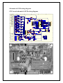
1
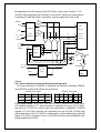
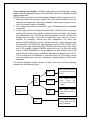
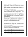
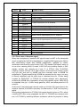
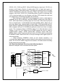
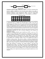
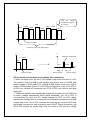
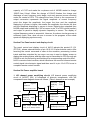
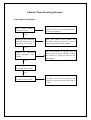
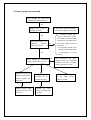
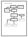
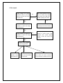
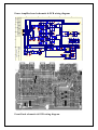
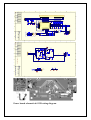
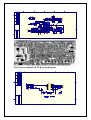
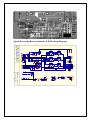
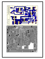
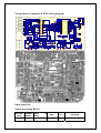
AV250T Service Manual
Contents
chapter One Brief Introduction to Product
General description
Chapter Two Operating Principle
Section One Overall structure
Section Two Volume board
Section Three Signal processing board
Section Four CPU board
Section Five Panel control and display circuit
Section Six Power amplifier board
Section Seven Power board
Section Eight Video board
Chapter Three Servicing Process
1. No output for Karaoke
2. Power supply not connected
3. No on screen display (OSD)
4. No output
Schematic & PCB wiring diagram
Spare parts list
Chapter One Brief Introduction to Product
General Description
AV110T is a 5.1CH audio power amplifier for home theatre usage, with the
main features and functions shown as follows:
1) Two-way audio signal input: VCD, DVD;
2) With 5.1CH input terminal, capable of connection with AC-3, DTS decode
output signal;
3) One way subwoofer signal line output, capable of connecting with active
subwoofer speaker;
4) Automatically signal search when power on;
5) 6CH digital volume control and separate channel level adjustment;
6) Three sound field modes: Hi-Fi, Standard and Cyber Logic;
7) Six preset EQ modes, multi-band electronic equalization adjustment snd
scene surround function;
8) Save/Call of user-set parameter;
9) Digital Karaoke, with microphone volume, echo and delay adjustment;
10) Auto mute function;
11) Dynamic display screen; multiple spectrum display modes; English
intelligent operation interface;
12) Bass enhancer function;
13) Digital tuning function;
14) Video switch function;
15) Headphone output function;
16) Full remote control operation.
Chapter Two Operating Principle
Section One Overall structure
The whole unit of AV250T is mainly composed of the following parts:
2.1.1 Volume board: input selection, Cyber Logic and bass enhancer control.
2.1.2 Signal processing board: Karaoke signal processing and front stage
amplifying of 5.1Ch signal.
2.1.3 CPU board: whole machine control unit, breadth sampling circuit and
auto searching circuit.
2.1.4 Control panel: VFD display, remote control and keyboard scanning and
fulfill man-machine conversation function.
2.1.5 Power amplifier board: perform power amplifying for 5.1CH signal or
other analog signals.
2.1.6 Power board: supply the working voltage required by each unit circuit,
and over-current/over-voltage protection unit.
2.1.7 Digital tuner: receive radio signal and then send to power amplifier to
perform signal-amplifying processing.
2.1.8 Video input and output board: fulfill video input/output and video switch
function.
Section Two Volume board
AV250T has 4 kinds of input modes in all: FM/AM, VCD, DVD and 5.1CH.
By sampling from L/R channel of AV250T, after Cyber Logic function, C, SL
and SW channel signals are achieved. In this circuit, electronic analog switch
is adopted to fulfill the switch in all states, and the signal flow chart is as
FM/AM
L
VCD
N106
CD4052
CD
5.l
15
M62446
Input
input
selection
L, R
Channel
5.1 input
R
13
SW
C
6
11
SR
8
SL
C, SR, SL
channel
SL
CD4053
SR
Electronic
c
Electronic
volume
adjustment
9
N108B
switch
N103A
N103B
5.1 input
SW CH
SW
CD4053
SEARCH
Send to L/R
Electronic
SW1
N100
CPU
switch
follows:
2.2.1 Input selection and sound field processing mode
The input selection of AV250T is achieved via electronic switches CD4052
and CD4053, and the truth tables are as follows:
CD4052 Truth table
CD4053 Truth table
Tuner
VCD
DVD
5.1
A
X
B
Y
C
Z
A
0
0
1
1
0
X0
0
Y0
0
Z0
B
0
1
0
1
1
X1
1
Y1
1
Z1
5.1CH input mode: Now A/B/5.1CH control pins of M62446 are in high level.
L/R channel signals of 5.1 input terminal is outputted from pin 3/13 of N101
and sent to IC N106 for volume and tone adjustment; meanwhile, C/SR/SL
signals of 5.1CH input terminal are outputted from pin 14/15/4 of N102 and
then respectively sent to IC N106 for independent volume adjustment. And SW
signal of 5.1CH is outputted via pin 4 of N103 and then sent to M62446 after
being amplified by N107A.
Three analog input modes: AV250T totally has three analog input modes:
digital tuning demodulation signal, VCD and DVD, which are controlled via A/B
signal respectively.
AV250T totally has three sound field modes: Standard, Cyber Logic and Hi-Fi.
1. Standard: Under the control of overall CPU, when bass enhancer is off, L/R
channel and subwoofer output are available; when bass enhancer is on,
only L/R channel output is available.
2. Hi-Fi: Under the control of overall CPU, only L/R channel output is available
to M62446.
3. Cyber Logic: Pin 9/10 of electronic switch N101 (CD4052) select a group of
analog L/R channel input signals according to the truth table. L/R signals
are outputted from pin 13/3 via the internal electronic switch of N101, and
divided into two ways. One way is respectively sent into pin 13/15 of
M62446 for electronic volume and tone adjustment. The other way
produces SW/S-SR/S-SL and S-C signals via buffer, adder-subtractor and
low-pass filter. S-C/S-SR/S-SL signals are sent to pin 12/2/5 of N102. N102
select Cyber Logic signal input (see CD4053 truth table) from Cyber Logic
and 5.1Ch signals, outputs C/SR/SL signals from pin 14/15/4 and sends
into pin 11/8/9 of M62446 for volume adjustment. Still another way of SW
signal directly sends to pin 6 of M62446 after being outputted from N107A.
5.1CH signal sent into M62446 is outputted from pin 31-36 after volume
and tone adjustment, and then outputted to signal board by XS20 power
distributor.
The relation between sound sources in input circuit and sound processing
modes is as the following figure.
Only L/R channel output.
Hi-Fi
Sound field and EQ setup
invalid
Two
analog
input
Only
Standard
modes
L/R/SW
output.
channel
Concert
hall
sound field and EQ setup
available
Press
INPUT
button to select
Cyber
circularly
Logic
5.1 input
mode
6CH
output.
Theatre
sound field and EQ setup
available
6CH output. Theatre
sound field and EQ
setup available
2.2.2 Control circuit
Pin 23/26/27 of CPU (N100) output data, PVST and clock signals send to pin
39/40/41 of M62446, control pin 1/2/3/4 of M62446 output control level, so as
to select input signal and spectrum sampling signal. It is worth noting that
PVST signal is a latch control signal. When data and clock of CPU are sent to
M62446, an identification signal will be added, indicating that this signal can
only be used by M62446 while other IC of I2C bus cannot use current data and
clock signal.
2.2.3 Frequency spectrum sampling circuit
Only S-C/S-SR/S-SL/SW signals are sampled during frequency spectrum
sampling in AV250T and added to pin 14 of N103 via a 150K sampling resistor.
Another S-C cyber logic signal is added to pin 1 of N103, called S-C'. 5.1CH
and LR-T of M62446 select sampling signals. When cyber logic is selected, the
control signal of 5.1CH is of low level while pin 9/11 of N103 is of low level.
According to the truth table, it is known that the outputs are X0/Z0. Sampling
signal is grounded while LR-T is of H level. Select Y1, S-C'signal is outputted
from pin 15 of N103 to N108B, adding to OK-R signal for the amplification of
frequency spectrum signal, and then sent to frequency point gating and auto
search circuits via XS20.
2.2.4 Tuning function
The tuning function directly controls tuner and receives audio frequency signal
mainly via CPU and then outputs after amplification via power amplifier. The
clock and data line of tuner are shared with LM62446 and the other two control
lines are connected to CPU directly. L, R signal processed by the tuner can be
sent to N101 IC CD4052 directly to input the selected channel.
Section Three Signal processing board
The signal processing board superposes, mixes and amplifies 5.1CH signal
sent from the volume board, voice signal from the voice board and Karaoke
signal.
2.3.1 Karaoke circuit of AV250T
This circuit processes human voice through power amplifier and reproduces it
via speaker. It includes human voice beautification circuit, wide sound field
processing circuit, Karaoke echo and delay adjusting circuit.
IC and its functions for Karaoke:
S.N. of IC
Name of IC
Functions of IC
N201
PT2308
Transmittal, pre-amplification for Karaoke signal
N200
PT2315
Karaoke volume control, including tone control
N205
CD4053
Electronic switch
N209
PT2399
Karaoke echo processing
N207
CD4051
Karaoke delay adjustment
N208
CD4051
Karaoke echo adjustment
N204
4558
PT2315 functional pin
S.N.
Name of pin
1
REF
2
VDD
3
AGND
4
TREB L
5
TREB R
6
RIN
7
LOUD-R
9
LOUD-L
11
LIN
12
BIN L
13
BOUT L
14
BIN R
15
BOUT R
16
RFOUT
17
LFOUT
18
DGND
19
DATA
20
LCK
8,10
NC
Phase inverter
Description
Reference voltage (1/2VDD)
Power supply
Analog
Treble control pin of L/R channel
R channel input
Loudness control pin of R channel
Loudness control pin of LR channel
L channel input
Bass control input/output pin of L channel
Bass control input/output pin of R channel
R channel output
L channel output
Digital
Control data of sequence transmission (DATA)
Clock input of sequence transmission
Not connected
2.3.2 Flow chart of Karaoke signal
When the microphone is inserted, MIC signal is sent via MIC to the transmittal
circuit combined by N201A for amplification. Amplified MIC signal gives CPU a
MIC identification signal after N202A amplification, followed by VD201
rectification and filtering control triode V200. CPU sends PKM signal, which is
of low level, causing cutoff of triode V103/V105 and enabling output of MIC
signals; another way reaches pin 6 and 11 of PT2315 after C219/C222
coupling, outputs from pin 16/17 after internal volume and tone control, mixed
into one way and sent to N202B and then reversely send to N203B for
amplification. Signals amplified by N203B are divided into two ways: one way
is directly outputted; and the other way is outputted from pin 14 after being
coupled by R222/C247 to PT2399 for internal delayed echo adjustment,
reversed by N204B and outputted by mixing with karaoke signal. While OK-R
is outputted from pin 14 after being gated by N205 and superposed to L/R
channel.
In this circuit, the bass boost network made up of triode V201 connected to the
negative terminal of N202B is primarily for bass boost of 75HZ low frequency
signal.
During delay adjustment for PT2399, first control signal is given to CPU, which
controls N207 after being expanded via N211 IC CD4094 and connects with
pin 6 of PT2399 by selecting different resistance values for purpose of delay
adjustment.
Echo control is to change the resistance value at the connection point to R229,
so as to change the superposition on through connect signal for echo control.
The wide sound field processing control signal of SOK’s karaoke is in wide
sound field mode when it is high level, and now the signal of OK-R is the OK
signal inverted by N204A.
A sense signal of OK-SW on the MIC plug detection together with the network
made up of V200. When MIC is not plugged, it is low level; when plugged, it is
of high level.
Karaoke auto mute function is also available. When P-KT fails to detect signal
for a continuous period, CPU will send a P-KM signal to mute karaoke and
avoid MIC receiving noise, which may affect on sound effect.
Signal flow chart of scene mode
AV250T has a special function that switching between 5 scene modes is
available without karaoke, which is fulfilled through part of karaoke.
When pin 9/10 of N205 are of high level, sampled L/R/C signals are outputted
via pin 3 through N205 gating. After amplification by N203, one way is
connected directly; and another way is sent to internal of PT2399 for echo
delay adjustment (controlled by IC CD4049), with the adjusted effect
superposed to L/R/C channel to form different scene modes.
In this circuit, MIC shall not be inserted and is only available in 5.1CH mode.
N203A is for the purpose of reversal.
In addition, this device is added headphone output function. PHSW is low level
and each channel has output when headphone is not inserted. But when
headphone is inserted, PHSW will be high level for the mechanical settings
thus LRM and SCM signals change into high level at the same time to realize
muting in each channel, so the signal is only outputted from headphone, that is,
there is not signal output with each channel when connecting with headphone
output.
2.3.3 Bass enhancer circuit
P-BURST is the switch signal of bass enhancer. When it is of high level and
added to the base electrode of V102, V102 will be switched into conduction.
When the collector electrode outputs low level, V107 will be cutoff; when the
collector electrode is of low level, V100 will also be cutoff. SW signal is
normally outputted to external terminal. Meanwhile, the high level signal of
P-BURST is added to the emitter electrode of V108. V108 is positively biased
and switched into conduction. The collector electrode adds high level to the
base electrode of V101. V101 is positively biased and switched into conduction,
and ground SW signal, not superposing it to L/R signal.
In reverse, when P-BURST is of high level, V100 will be switched into
conduction and SWM cannot be outputted from external terminal. Meanwhile,
V101 is cut off and SW signal is superposed to L/R channel signal.
The bass enhancer of AV250T can be divided into three steps. This principle is
to change the volume of bass enhancer by changing the SW output volume of
M62446.
2.3.4 Mixing and amplification circuit of 5.1 signal and karaoke signal
When L/R channel signal of 5.1 signal is superposed with SW signal and
amplified by N101B/N100B, it is sent to the reverse phase of N101A/N100A.
Meanwhile, OK-R/OK-L signals are also respectively added to the reverse
phases of N101A/N100A. After mixing and amplification by N100A/N101A,
they are respectively outputted from pin 1 of N100A/N101A to power
amplification circuit for power amplification.
Meanwhile, the C-1 signal sent by volume board is added to the reverse phase
of pin 6 of N102B and added to the reverse phase of N102A after amplification.
Now C1-1 signal after electronic echo processing is also added to the reverse
phase of N102A and sent to power amplification circuit after mixing and
amplification.
SR-1/SL-1 of another volume board is also added to the reverse phase of
N103B and N104B for amplification and then sent to N103A and N104A for
further amplification, and later sent to power amplification circuit.
One way of 5.1 signal after being mixed and amplified is sent to power
amplification circuit passing through XS9, and the other way forms DIST
(distortion
error
detecting
signal)
signal
passing
through
R111-R113/R142/R145/VD100-VD104, which will be added to CPU for
automatic gain adjustment, so as to control volume output.
Section Four CPU board
2.4.1 CPU control unit
N100, the overall CPU, is the overall control center, inputting all kinds of
control instructions to controlled circuits to achieve all kinds of control functions.
It adopts +5V supply with pin 40 as its supply pin. Pin 18 and pin 19 connect
externally with 12M crystal oscillator to provide working clock frequency for
itself. Pin 9 is its reset pin. When starting, +5V charges C106 via R100. The
voltage of two ends of capacitance cannot be mutated, thus B-pole of triode
V100 is low level, that is, V100 conduction gives a high-level reset signal to
CPU. When capacitance C106 finishes charge, V100 stops and then reset
finishes. The form of this reset circuit is to reset high level and keep low level.
When the machine is working, the static information of Power-on logo on
screen and Chinese characters are stored in CPU internal static memory.
N101, a status memory, can record the current working status of machine
when powering off and show the status when next time power on, avoiding
users to re-adjust. The sound field mode set by users is also stored in it and
can be called when necessary.
2.4.2 Detect input signal and automatically search circuit
DISPLAY signal from volume board is sent to N103A to amplify and limit level,
and then sent to inverse end of voltage comparator N103B after capacitance
coupling. It inputs from pin 7 of N103B and then is sent to pin 16 of CPU via
VD103, V101, R109 and R107. When N103B inputs a high level, VD103 is in
reverse cut-off status, B-pole of switch tube V101 is high level and is in
conducting status, then gets an about +5V high level (signal input) to CPU after
VD101’s stabilization and stop searching. When the output end of N103B
outputs a low level, VD103 is in conducting status, B-pole of switching tube
V101 is low level and is in cut-off status, and then CPU detects the low level
(no signal input). Its working principles are as follows:
① After starting up, under CPU internal program’s control, a data signal is
outputted via pin 23 to M62446, and then M62446 scans each input port of
N101, N102 and N103 by emitting high and low levels. When the input ports
have no signal input, it automatically becomes standby status. When any of
ports has signal input, channel paths of input N101, N102 and N103 has A/C
signal which is amplified and limited level by N108B and N103A of CPU board,
then compares with pin 5 of N103B and gets plus-minus level close to supply
power. The co-phase voltage of N103B is about 0.1V. After the direct current
voltage is over 0.1V, the output end of N103B outputs low level is close to
negative-power voltage, VD103 positive-bias conducts, switch tube V101
(S9014) stops, emitter outputs a low level to pin 16 of CPU which by controlling
IC M62446 makes search level lock on the port through which signal inputs, to
enter normal play.
② When pressing “SEARCH” button on the remote controller, it is
converted from optical signal to electric signal by the remote control receiver of
panel. Pin 14 of CPU emits a high level to conduct V102 and search according
to the same previous process.
2.4.3 Spectrum Analysis Circuit (see the following figure)
Spectrum analysis circuit is divided into three parts:
N105C
DISPLAY
35HZ
3
N104
N108
.
+
134HZ
300HZ
CD4051
1KHZ
Auto
2.2KHZ
and
gain
CPU
Frequency
point
spectru
m
}
CD4051
6.3KHZ
}
adjustme
gating
3
16KHZ
CPU
7-segment
band-pass
N102A
V105
+
.
Pin 12 of CPU
+5V
V103
V104
Pin 28 of CPU
A/D conversion
Automatic spectrum gain adjustment circuit: To avoid two situations that
spectrum display amplitude is too low when input signal is too weak or
spectrum display is in full screen when input signal is too strong, AV250T sets
automatic spectrum gain adjustment circuit, using a single-track
one-from-eight electronic analog switch, its true value diagram is as follows:
CD4051Truth table
X0
X1
X2
X3
X4
X5
X6
X7
A
0
1
0
1
0
1
0
1
B
0
0
1
1
0
0
1
1
C
0
0
0
0
1
1
1
1
Its main working principle is to change the value of inverse ground resistance
of transmittal N104 to change the transmittal gain multiple. Let’s see the
detailed work of the whole circuit. We’ve referred that spectrum analysis signal
source (DISPLAY) is sent to the co-phase input end of transmittal N105C to
amplify. Its amplification factor is determined by the value of the resistance
connecting with the electronic switch of its inverse end N104. When the main
volume is large, CPU will automatically increase the value of ground resistance
and decrease the amplification factor; when the main volume is small, CPU will
automatically decrease the value of ground resistance and increase the
amplification factor.
Amplitude sampling circuit: signal amplified by N105C is sent via C115
coupling to seven band-pass filters composed of transmittals. By setting its
capacity of feedback capacitance, its frequency-band range can be determined.
The frequency value of superscript of the output points is the central
frequency-point of the frequency band. The output end of each band-pass filter
is connected with a half-wave rectifier circuit. The amplified A/C signal is
rectified to direct current. The circuit is mainly to achieve frequency-point
sample. It can display the amplitude of all frequency-points of the whole sound
signal via direct-current voltage. If the low frequency of sound signal is stronger,
the current voltage of output end of 35HZ and 100HZ band-pass filter is higher.
When high frequency is stronger, the current voltage of 10K and 16K
band-pass filter is higher. The output ends of the seven band-pass filter are
connected with the seven input ends of electronic switch N108 (CD4051).
These electronic switches will quickly circularly-switch among frequency points
(referring to previous true value diagram). Pin 3 output end of N108 will output
a string voltage value representing frequency point signal amplitude (see next
diagram).
Note:
V
the
voltage
amplitude in diagram
35HZ
100HZ
1KHZ
300HZ
10KHZ
3KHZ
is uncertain.
16KHZ
35HZ
T
Interval of switch
Frequency point cycle gating period
V
V
Discharge of high level
100HZ
35H
35H
100HZ
T
T
Interval of switch
Time for charge
Time for charge
A/D conversion and output circuit display (two situations):
1. When no signal input, pin 28 of CPU sends a high level to B-pole of V104.
The positive end of N102B is low voltage, the inverse end of N102B gets
partial voltage of R189 and R172, making N102B output a low level, that is,
triode V105 stops and C-pole of V105 will give a high level to pin 12 of CPU to
let CPU not conduct AD conversion (pin 6/7/8 of CPU are inactive and keep
high level).
2. When the machine has detected the signal (the inverse end of N102B has
a current voltage representing 35HZ signal amplitude), pin 28 of CPU is
converted into low level and +5V voltage charges for C137 via V103. When
reaching the voltage value of inverse end, the comparator converts and N102B
outputs high level. Once CPU receives low-level signal, it stops 35HZ level
gating and converts into next frequency point 100HZ. During conversion, pin
28 of CPU outputs an instant high level to conduct V104, leak the voltage
capacity of C137 and make the co-phase end of N102B restart to charge
100HZ from 0-level. When the charge of 100HZ finishes, the charge and
discharge of next frequency point begin, and such process occurs circularly
under the control of CPU. The charge time form 0-level to the occurrence of
output conversion represents the signal amplitude of current frequency
point—the larger the amplitude, the longer the time and the amplitude
displaying in screen is higher; the smaller the amplitude, the shorter the time
and the amplitude displaying in screen is lower. Digital pulse outputted from
N102B output end is added by V105’s inverse to pin 12 of CPU which handle it
and output to panel to display dynamic frequency in screen. The display of
original frequency points is sequential. However, the above circular process is
extremely quick, thus, what we see in screen is the progress of the whole
spectrum displaying synchronously.
Section Five Panel control and display circuit
The panel control and display circuit of AV110 adopts the special IC 101
(PT6311), whose external buttons of pin 10/11/12/13 scan buttons matrix. After
receiving the control command of users to the machine, processing is done
inside and then outputted by two ways: one way is sent to display screen to
display the working status; and the other way is transmitted to CPU through pin
5/6/8/9 to ask for performing and finishing the corresponding control function.
N102 is remote control receiver, which transforms the received infrared remote
control signal into electronic signal and then send it to pin 13 of CPU so as to
complete remote control function.
Section Six Power amplifier board
1. L/R channel power amplifying circuit: L/R channel power amplifying
circuit of AV250T (RU) is composed of discrete components, with the
composed frame diagram shown as follows. (Take L channel as an example)
AC
negative
feedback
Voltage
amplifying
Differential
amplifying
V101
V102, V103
stage
power
amplifying
V132,
V112
R121, R108, C105
L-in
Composite
stage
V105
.
Temperature
compensation
stage
Speaker
V106
V115
Relay
Mute
Mirror image constant source
V104, V107, VD102, VD103
Composite
power
amplifying V133, V113
L channel signal is sent to pole B of differential amplifying stage V102 after
being coupled by R101, R103 and C101; V102 and V103 compose single
ended input/output differential amplifying circuit. Sound signal outputs from
pole C of V102 to pole B of voltage amplifying stage V105, and then outputs to
composite power amplifying stage after voltage amplifying. V104, V107,
VD102 and VD103 compose mirror image constant source circuit. VD102,
VD103 provide V104, V107 with constant base electrode current. Emitter
resistor of V104 determines working current of differential amplifying stage;
and emitter resistor of V107 determines working current of voltage amplifying
stage. V132 and V112 compose multiple unit tube amplifying to supply strong
current amplifying capacity for final stage of power amplifier, which composes
waveform positive half cycle amplifying. V133 and V113 compose waveform
negative half cycle amplifying and the circuit structure is the same with the
above. The function of temperature compensation tube V106 in circuit has two:
it is the base bias of geminate transistors firstly and its working state
determines the static working current of composite power amplifying stage,
that is, through adjusting the gating degree of V106, we may set the static
working point of composite power amplifying stage. The usual means is to
change the base electrode resistor of V107; it may also automatically adjust
the working state of composite power amplifying stage after the temperature
increases, with the adjustment process shown as follows:
Total current of output stage = working current + leakage current
When temperature increases, the increase of leakage current leads to drift
of static working point, and meanwhile leakage current of V106 increases. The
decrease of Uce makes the bias current of output stage decrease, the working
state change and the working current of back stage decrease to achieve the
function of temperature compensation.
Introduce voltage negative feedback into power amplifier circuit of AV250T,
composed of R121, R109, C105, which is capable of stabilizing static working
point of differential stage. AV250T adopts direct output means and R111, C116
connected to output terminal compose Joubert Network, capable of avoiding
high frequency self-excitation caused by the AC inductive reactance of
speakers voice coil.
Mote control: when pressing MUTE button on remote controller, a mute
signal, achieved through signal photoelectric conversion performed by remote
control receiver, is sent to CPU, and then a high level mute order is outputted
from pin 35, 36 of CPU to make V115, V101 and V116 on, left/right channel
signal has short circuit to ground to fulfill mute control function.
C, SR, SL power amplifying circuit: compared with the former models,
the three channels of AV250T adopt special power amplifiers LM1876 and IC
LM1875. As for LM1876, it has 15 pins in all, in which pin 2, 15, 4 are its
positive/negative power pin; and pin 7, 8, 12, 13 are its in-phase or reverse
input terminal. The rated output power of each channel of this power IC may be
up to 20W, with auto mute function when power on; as for 1875, it has 5 pins in
all. It is a good performance power amplifying IC, with very simple application
circuit and 15W power output in rated state. Pin 5 and 3 are positive and
negative power supply pin.
Section Seven Power board
Power board supplies working voltage required by each unit circuit and
over-current/over-voltage protection unit. Protection unit circuit is emphasized
here.
The protection means of L, R, and C channel is fulfilled through
disconnecting relay Y100 when starting up so as to disconnect the output. SR
and SL channel achieves protection function through mute. AV250T is with
power-on protection, central point over-voltage-over-current protection and
standby protection.
1. Power-on delay attracting protection circuit:
The working of circuit is unstable when power on and the generated
percussive current does great harm to speaker and power amplifying circuit, so
delay attracting protection circuit is set. This circuit is divided into two steps:
1) C, L, R. The working process is: a 22V voltage is achieved after AC
outputted by transformer being rectified and filtered by VD113, C110, and
then charges C115 through R108 to make VD111 struck through reversely
and make V105 and V104 in-phase on to finally make Y100 attract to reach
delay effect.
2) Surround left and right channels perform anti-percussion protection when
power on: after machine system resets, pin 33 of CPU outputs a high level
to pin 9, 14 of LM1876 through R164 to make LM1876 output mute. After
delay start-up of machine succeeds, pin 33 of CPU converses to low level
immediately and outputs normally through SL/SR channel.
2. Central point over-voltage protection:
An over-voltage sampling resistor is connected to the output terminal of
each channel. L channel is R116, R channel is R117, C is R118, SR and SL
channels are R119 and R120 respectively. Only when one channel’s central
point voltage is above +3.5V or below -3.5V, V101 or V102 is on to make their
C pole voltage decrease, then V103 on, relay disconnected and protection
circuit start up finally.
Over-voltage
sampling resistor
is connected to
each channel
When
L
above
C
+3.5V
channel
is R116
Relay
V101 on
pole
voltage
When below
+3.5V
V102 on
decrease
disconnect
V103
on
and protection
start up
Over-current and short circuit protection:
An over-current sampling triode is connected to the output load resistor of
L/R channel. Sampling tube of L channel is V114 and load resistance is R126
and R127. The other three channels’ power amplifying IC is with over-current
protection inside. Only L channel appears over current, the pressure drop
produced on R126 and R127 will increase quickly. Once the pressure drop on
R129 is above 0.7V, V114 will be on, and V103 is also on. Finally relay
disconnects and protection circuit starts up.
Pressure drop
Over-current
sampling
L
triode
is
channel
connected
to
is V114
each channel
on
R126,
R127
increases
when
over
Relay
V114
C
is on
voltage
pole
decrease
V103
is on
disconnects
and protection
starts up
current
The same, when R channel has over current, voltage on R159 will be above
0.7V to make V129 on, and then V103 on. Finally relay disconnects to reach
the purpose of protecting speaker.
4. Standby protection:
When standby time is up to 10 minutes and standby by force is needed,
PRC signal outputted from pin 34 of CPU is high level, which makes V100
saturated and on through VD108, R101 to make V103 on. Finally relay
disconnects to reach the result of standby and energy saving.
Section Eight Video board
Video board fulfills the functions of input, output and switch of the video, with
the schematic diagram shown as the following figure:
This switch function is realized through an electronic switch IC CD4051. When
high and low level of control signal A and B are changing, IC CD4051 switches
between VCD and DVD, and video signal is outputted by pin 3 VOUT.
Chapter Three Servicing Process
1. No output for Karaoke
Firstly
confirm
Note: For MIC size is disordered on the market,
whether
that MIC is too long or too short will both lead to
microphone is good.
no output of microphone.
Yes
Whether the pre-amplification
Note:
here
please
check
whether
the
circuit and checking circuit of
microphone checking signal P-KT is able to
microphone work normally.
overturn when signal output is available.
Yes
Whether
volume
the
microphone
adjustment
works
normally.
Note: check whether the periphery circuit of
volume boost IC2315 or IC M62429 is normal,
and whether the voltage and data line has
abnormalities.
Yes
Whether high/low frequency
boost circuit works normally.
Yes
Whether
mute
circuit
microphone works normally.
of
Note:
check
whether
the
triode
in
the
microphone mute circuit has damage, and
whether the mute control signal line P-KM is
normal.
2. Power supply not connected
Check whether the power cord
socket has been well connected.
Yes
Whether
fuse
FL100
is
No
complete and good.
In most cases, primary short-circuit
of transformer will burn out this fuse.
1. If primary internal short
Yes
circuit of transformer occurs,
the resistance numerical value
will decrease, fuse will be burnt
Check the primary coil
resistance
No
numerical
and power supply will not be
connected.
value of transformer.
2. The primary internal circuit
opening of transformer leads
Yes
to disconnection of power
supply.
Check whether the secondary
No
voltage of transformer is normal.
The
short-circuit
and
circuit
opening inside the transformer
secondary coil lead to abnormal
output of secondary voltage.
Whether the input and
output of three-terminal
voltage regulator are
abnormal.
Whether
secondary
the
fuse
is
complete and good.
Whether power supply
Whether
the
output
voltage of pin 40 of CPU
voltage of rectifier tube
is normal.
is normal.
Whether the control panel
IC
and
display
voltage is normal.
screen
3. No on screen display (OSD)
Check
whether
filament
the
voltage
Note: If display screen has
No
of
display screen is normal.
air leakage, it will cause no
OSD and now the filament
No
voltage is close to be low.
Yes
Note: The abnormality of
the
secondary
voltage
of
output
No
transformer
may probably cause no
Whether the power of
control
panel
IC
is
normal.
OSD.
Yes
Check whether the data line
No
between CPU and control
Whether CPU power
panel drive IC and clock line
supply is normal.
signals are normal.
Yes
Yes
Whether signals from control
panel drive IC to display screen
No
pin are normal.
the badness of control
panel drive IC.
Can
Can
judge
that
display screen is
not good.
judge
that
the
problem occurs in CPU
board.
Yes
May probably cause
Yes
4. No output
Check whether the analog
electronic switch IC can be
Note: check whether IC power
No
cord is normal, and signal
gated in this path when there
cords P-INA and P-INB which
is signal input.
control IC gating are normal.
Yes
Yes
Check whether tone adjustment
Check
whether
power-on
IC62446 or 75347 front stage
checking circuit works normally.
has signal input.
Yes
Check periphery circuit of IC is
Check whether tone adjustment
No
normal; IC power supply; and
IC62446 or 75347 front stage
whether
CPU
control
signals
has signal input.
P-VDA, P-VCK and P-VST are
normal.
Yes
Whether power amplifier
board has signal input.
Whether power
Check whether power
Whether main channel mute control
amplifier board
tube has abnormalities
line P-LRM and center surround
has signal input.
of punch hole.
mute control line P-CSM are normal.
Schematic & PCB wiring diagram
CPU board schematic & PCB wiring diagram
A
B
C
D
E
F
更 改
设 计
154
14
VD114
1N4148
R165
1K
N106D
LM324
35Hz
C151 103
+12V
C132
R159
100K
9
10
R158
4.7K
R181
100
683
C131
683
R157
10K
DIST
VD113
1N4148
8
R160
1K
N106C
LM324
C129
223
11
N106A
LM324
300Hz
R156
10K
C130
2.21u/50V
4
VD111
1N4148
7
R151
1K
日 期
批 准
N106B
LM324
-12V
1KHz
R186
10K
C127
2.2u/50V
C123
472
C122
472
VD110
1N4148
7
5
R146
1K
N105B
LM324
R209
2.2KHz
C124
2.2u/50V
R193
+5V
11
C145
103
-12V
N105A
LM324
R142
10K
+12V
14
VD108
1N4148
N105D
LM324
X0
14
R136
1K
16KHz
R137
10K
X2
12
1
12
27K
R125
1
5
4.3K
R123
2
2.2K
R122
1.5K
4
VCC
X2
X3
GND
INH
X4
VEE
A
B
C
X7
N104
CD4051
R173
11
10
9
0.22u/16V
C137
0.1u
P_ADSELA
P_ADSELB
P_ADSELC
VD115
R178
10K
7
P_KCK
6
P_KDA
5
TEST
A1
SCL
A2
SDA
VSS
2
R104
0
3
4
24C02
V103
2N5401
5.6K
+5V
A
B
C
C138
V105
9014
1
VD116
1N4148 1N4148
R174
4.7K
V104
9014
R175
P_CHARGE
2.2K
R+5V
C113
10P
16
8
+6.8V
R118
470/0.25W
+12V
VD106
6.8V
C111
10u/16V
8
6
R117
+12V
+12V
103
N103A
3
4558
C110
4.7u/16V
1
6
2
C112
10u/16V
C150
VD107
6.8V
11
10
9
-6.8V
R119
470/0.25W
-12V
VD103
N103B
4558
7
1N4148
C109
2.2u/50V
R110
22K
-12V
R116
C105
103
V101
9014
5
10K
R111
4.7K
R113
180K
470k
-12V
P_SELECT
VD102
1N4148
R100
22K
C107
104
RESET
R112
2.2K
9014
V100
9014
R109
15K
R107
V102
R114
1.5K
P_GNA
P_GNB
P_GNC
R101
4.7K
+12V
47K
R115
103
7
X5
X6
-12V
103
R177
1K
R172
10K
C148
-6.8V
1N4148
7
A0
R211
4.3K
C106
4.7u/16V
P_SEARCH
100
VD101
4.7V
R108
10K
R189
10K
6
6
版次:1.0
10K
R124
X1
8
6
7
P_ADINT0
VD118
N102B
4558
6
5
C149
3
4
共 1 张
15
75K
R126
VEE
VD117
3.3V
R170
1K
VDD
5
第 1 张
BBK
5
东莞市步步高视听电子有限公司
14
180K
R127
X
GND
INH
X4
X7
470K
X0
R169
470K
N102A
3
100K
+6.8V
N101
CD4051
R130
13
C154
221
8
C108
104
9
R131
10K
10u/16V
470K
R128
X3
X6
4
8
22K
R129
R194 100
+5V
R179
10K
1
16
X5
2
N105C
LM324
10
3
CON15
RR101
8*4.7K
+12V
R1672
VCC
5
R132
X
X1
15
C118
2.2u/50V
C115
10u/16V
C114
P_VCK
P_VST
P_KM
P_HOLD
P_VDA
P_KCK
P_KDA
1
2
3
4
5
6
7
8
9
10
11
12
13
14
15
4
4
12
N108
13
R135
100K
C156
221
P_CHARGE
R199
470
R195
470
R196
470
R192
470
R191
470
R198
470
R197
470
+5V
4558
DISP
DIST
P_CSM
P_LRM
P_RC
P_RLY
P_SCART
P_VCK
P_VST
P_KM
P_KCK
P_KDA
P_LDA
P_HOLD
P_VDA
P_GNA
P_GNB
P_GNC
P_CSM
P_LRM
P_RC
P_RLY
P_SCART
470
470
100
+5V'
C147
C121
2.2u/50V
561
13
DISPLAY
P_KT
R168 10K
C104
30P
12M
103
C117
C116
561
R134
4.7K
6.3KHz
+12V
103
R133
10K
R141
1K
8
C146
R187
XP101
R202
R201
R200
G100
C103 30P
4
R139
4.7K
1M
40
39
38
37
36
35
34
33
32
31
30
29
28
27
26
25
24
23
22
21
10K
VD109
1N4148
1
3
+5V
R140
100K
2
4
C119
152
R138
10K
22
R210
P_LDA
4.7K
152
P10(T2)
Vcc
P11(T2) P00(AD0)
P12
P01(AD1)
P13
P02(AD2)
P14
P03(AD3)
P15
P04(AD4)
P16
P05(AD5)
P17
P06(AD6)
RST
P07(AD7)
P30(RXD) EA/Vpp
P31(TXD)
ALE
P32(INT0)
PSEN
P33(INT1) P27(A15)
P34(T0) P26(A14)
P35(T1) P25(A13)
P36(WR) P24(A12)
P37(RD) P23(A11)
XTAL2
P22(A10)
XTAL1
P21(A9)
GND
P20(A8)
8
7
6
5
4
3
2
1
0
R147
10K
C120
1
2
3
4
5
6
7
8
9
0 10
470 11
12
13
14
15
16
17
18
19
20
470
470
470
470
P_ADINT0
P_REM
P_SELECT
P_DIST
P_SEARCH
P_LDA
CON15
R145
100K
6
R144
4.7K
104
3
3
R143
10K
C155
C142
103
8*4.7K
R203
P_DST1
R204
P_DST2
R205
P_DDA
R206
P_DCK
P_KT
P_ADSELA
P_ADSELB
P_ADSELC
RESET
P_BURSTR207
P_BCK R208
-12V
GND
+12V
D+5V
GND
R+5V
P_DST1
P_DST2
P_DDA
P_DCK
P_KT
P_GNC
P_BURST
P_BCK
P_REM
1
2
3
4
5
6
7
8
9
10
11
12
13
14
15
C141
100u/16V
R150
100K
+5V
L101
N100
W78E58
XP100
C140
100u/16V
+12V
5
C102
104
RH-357508
22K
+12V
C126
6
R149
4.7K
C100
47u/16V
100uH
R183
+12V
R155
1K
103
C125
103
L100
RR100
VD112
1N4148
C144
R148
10K
D+5V
220
1
103
P_DIST
R185
4.7K
1N4148
C152 103
R182
100K
3
N107A
4558
-12V
-12V
2
R153
4.7K
2
R180
22K
C133
2.2u/50V
R154
C128 103
223 C143
R152
10K
R184
5.6K
VD119
1
C139
22u/25V
134Hz
R161
10K
3
2
2
数 量
更 改 单 号
签 名
审 核
标 准 化
C136
2.2u/50V
R166
10K
0
1
2
3
4
5
6
7
8
12
R163
4.7K
8
R164
100K
13
4
154
1
1
李林存
10-Mar-2006
C135
C134
R162
10K
R120
0
A
B
C
D
E
F
Power Amplifer board schematic & PCB wiring diagram
A
B
C
D
E
F
更 改
设 计
1
R117
R106
2K
V132
R113
150
VD104
V112
2SC5200
2SC5248
1N4148
R128
R103
10K
1K
R102
100K
C101
10u/16V
V102
2N5551
V103
2N5551
R104
47K
C104
220p
R108
47
R107 47
1
2
3
4
5
6
7
CON7
XP13
日 期
批 准
1
2
3
4
5
R109 1K
C105
100u/16V
SWM
L1
R1
C1
SL1
SR1
GND
C109
47n
C107
47u/100V
C110
0.47u/16V
33K
R122
100/0.25W
V107
2N5551
1K
VD102
1N4148
R126 R129
0.25/7W 1.5K
R121
R112
V104
2N5551
4.3K
R120
100/0.25W
4.7K
R127
0.25/7W
R130
4.3K
R110
510 VD103
1N4148
R116
150
V133
V113
2SA1943
2SA1964
Vs+
R183
Vc-
C113
47u/100V
R147
Vc+
V134
2SC5248
R131
10K
R133
1K
R162
10K V116
S8050
VD107
V127
2SC5200
1N4148
R158
V115
2N5401
C121
22u/16V
R143
150
R132
100K
C111
10u/16V
V117
2N5551
R134
47K
C114
220p
V118
2N5551
R138
47
R137
47
R139 1K
C115
100u/16V
R141 R144
33K/0.5W
V121
2N5551
R145
2.2K
R142
V119
2N5551
1K
VD105
1N4148
4.7K
Vs-
R156 R159
0.25/7W 1.5K
R184
2
Vin
47/3W
V129
2N5551
4.3K
R150
100/0.25W
C149
100u/16V
C139
47n
Vs+
R163
R164
10K
R166
10K
VD111
1N5404
C141
4700u/35V
VD112
33K
R152
100/0.25W
V122
2N5551
R157
0.25/7W
C159
V135
1N5404
V128
2SA1943
2SA1964
R155
C140
C142
47n 4700u/35V
Vs-
TC101
10u/16V
V137
R187
C9015
100K
R189
10K
R188
22K
R186
10K
VsR190
22K
TC104
1N4148
10u/16V
V131
S8050
V130
2N5401
R168
10K
2
R169
47K
C125
4.7u/16V
33K
820
C126
68p
7
S/M
IN
VD114
1N5404
FL102
T6.3A250V
C161
473
XS8
L2
R2
C2
SL2
SR2
GND
+Vs
N/P
4
3
2
R193
47K
C160
22p
TC105
Vc+
Vc-
47u/35V
1
2
3
4
5
6
7
8
9
CON9
TC106 47u/35V
1
TDA7298
C128
Vs-
-Vs
N/M
OUT
R192
22K
N104
LM1875
R171
R170
820
6
3
共 12 张
C122
22u/16V
V136
S8050
TC103
0.47u/50V
4
4.7K
VD115
47n
1
5
R191
3.3U/16V
Vs-
5
C124
1
2
3
N105
TC102
10u/25V
C127
R167
CON3
5
第 5 张
5
Vs+
C162
473
Vs-
C164
473
N106
R194
22K
47n
TC110
3.3U/16V
版次:0.0
TC109
0.47u/50V
5
R195
820
6
7
-Vs
N/M
S/M
IN
+Vs
N/P
OUT
R196
22K
TDA7298
4
3
2
TC107
47u/35V
TC108
47u/35V
Vs+
C165
473
1
6
6
东莞市步步高视听电子有限公司
BBK
VD116
1N4148
XS5
C144
0.1u
Vc-
10K
10K
C143
0.1u
1N5404
VD113
10u/100V
R160
R185
R165
4.7K
FL101
T6.3A250V
R151
C119
47n
R146
150
Vs+
1
2
3
4
CON4
3
Vout
N102
L7912
C120
0.47u/16V
220/0.5W
Vs+
+12V
DGND
DGND
-12V
C151
47n
4.3K
R140
510 VD106
1N4148
XP6
C150
47n
4
4
C117
47u/100V
V120
2N5401
C118
33p/500V
C147
220u/35V
3
3
R161
4.7K
CON5
R136
2K
3 100u/16V
Vout
220u/35V
220/0.5W
R135
2K
C148
Vin
C146
220/0.5W
GND
P_Rly
P_RC
P_LRM
P_CSM
N101
L7812
1
47/3W
R125
12
XP9
V105
2N5401
C108
33p/500V
R111 R114
33K/0.5W
V106
2N5551
R115
2.2K
1
2
3
4
CON4
V114
2N5551
GND
R101
V101
S8050
VD101
1N4148
XS7
2
2
数 量
更 改 单 号
签 名
审 核
标 准 化
SWM
Rly0
P_RC
Over
Vc+
220/0.5W
R105
2K
GND
1
卢建强
11-Mar-2006
C103
47u/100V
R197
C163
A
B
C
D
E
F
Front Panel schematic & PCB wiring diagram
47K
22p
A
B
C
D
E
F
1
45
46
F
F
G15
G14
G13
G12
G11
G10
G9
G8
G7
G6
G5
G4
G3
G2
G1
29
30
31
32
33
34
35
36
37
38
39
40
41
42
43
P13
P12
P11
P10
P9
P8
P7
P6
P5
P4
P3
P2
P1
4
5
6
7
8
9
10
11
12
13
14
15
16
F
F
G15
G14
G13
G12
G11
G10
G9
G8
G7
G6
G5
G4
G3
G2
G1
签 名
5
4
3
2
1
2
CON5
R101
2.2/0.25W
VD101
5.6V
R102
4.7k/0.25W
26
25
24
23
22
21
20
19
18
17
16
15
14
日 期
Ve
VD103
30V
C110
47u/35V
C101
47n
G1
G2
G3
G4
G5
+5V
Ve
G6
G7
G8
G9
G10
27
28
29
30
31
32
33
34
35
36
37
38
39
SG13/GR16
SG14/GR15
SG15/GR14
SG16/GR13
SG17/GR12
SG18/GR11
VDD
VEE
SG19/GR10
SG20/GR10
GR8
GR7
GR6
13
12
11
10
9
8
7
6
5
4
3
2
1
K4
K3
K2
K1
STB
CLK
NC
DIN
DOUT
SW4
SW3
SW2
SW1
S101
KEY
S102
KEY
S103
KEY
S104
KEY
S105
KEY
R104
100
R106
10k
R105
100
R107
10k
R111
100
R112
10k
+5V
C103
221
R108
10k
C104
221
R109
10k
C105
221
R110
10k
G11
G12
G13
G14
G15
40
41
42
43
44
45
46
47
48
49
50
51
52
4
4
N101
PT6311
C102
47n
3
3
R103 270/0.5W
C109
100u/35V
SG12/KS12
SG11/KS11
SG10/KS10
SG9/KS9
SG8/KS8
SG7/KS7
SG6/KS6
SG5/KS5
SG4/KS4
SG3/KS3
SG2/KS2
SG1/KS1
VDD
批 准
+5V
VD102
1N4004
GR5
GR4
GR3
GR2
GR1
VDD
LED5
LED4
LED3
LED2
LED1
GND
OSC
2
标 准 化
更改单号
审 核
数 量
XS101
1
2
设 计
更 改
1
李林存
10-Mar-2006
VFD101
VFD210T
+5V
R117
+5V
VD104
LED
XP103
1
2
3
CON3
共 12 张
VD105
LED
R118
180
180
R116
XS103
1
2
3
+5V
CON3
R114
180
R115
180
180
2
VS
XP102
OUT
8
7
6
5
4
3
2
1
1
GND
VD108
LED
+5V
VD107
LED
C107
47n
C108
47u/16V
REM
CK3
DA3
ST3
ST4
DGND
+5V
5
BBK
第 10 张
5
东莞市步步高视听电子有限公司
C106
47u/16V
R113
N102
REMOT
3
47k
CON8
VD106
LED
6
版次: 0.0
6
A
A
B
D
B
D
E
C
E
F
C
F
设
更 改
1
计
1
李林存
10-Mar-2006
8
审
数 量
D+5V
C106 330u/16V
1
C103
2
R103 4.7K
R109
47K
4
R101
47K
10u/16V
2
2
签
标 准 化
更改单号
核
N100A
PT2308
3
D+5V
X100
XP24
名
R105
47K
日
批
D+5V
DGND
R
L
PH_SW
1
2
3
4
5
期
准
PH_R
PH_L
C105 10u/16V
CON5
R106
47K
C102
100u/16V
MIC
N100B
PT2308
C107
3
3
5
7
6
330u/16V
C104 10u/16V
R102
47K
R110
47K
R108 10K
PH_SW
4
4
AV110T咪座板原理图
R104 4.7K
9
8
7
6
5
4
3
2
1
R107 10K
C100 103
C101 103
5
BBK
第 1 张
5
XP12
共 1 张
4
3
2
1
MIC1
GND
GND
MIC-DET
CON4
6
版次: 1.0
6
东莞市步步高视听电子有限公司
R100 22K
MIC1
A
B
C
D
E
F
Power board schematic & PCB wiring diagram
A
B
C
D
E
F
1
设
更 改
1
计
审
数 量
C100
22n
VD100
1N5404
核
VD101
1
2
VD102
1N5404
From TRANS
CON2
XS3
CON2
22n
FL101
C103
0.22u
XS4
~V1
0
~V1
V-RLY
TO TRANS
CON2
1
2
3
4
T8AL250V
Vc+
C108
8200u/63V
VD103
1N5404
C106
0.1u
VD104
1N5404
C104
0.22u
CON4
签 名
标 准 化
~220V 50HZ
C102
CT7 472
TO SWITCH
2
2
更改单号
C101
1
2
T6.3AL250V
2
1
1N5404
XS2
FL100
XS1
C109
8200u/63V
VD105
1N5404
FL102
T8AL250V
C105
22n
C111
22n
C107
0.1u
Vc-
VD106
C123
1N5404
批
VD113
From AMP
IN4148
R101
10K
C122
104
R104
R106
4.7K
3
准
日 期
3
1K
RLY0
SWM
C112
IN4148
R102
VD108
4
3
2
1
103
1N5404
VD110
47/3W
XP7
OVER
P_RC
RLY0
SWM
VD107
C110
100u/35V
R100
1N4004
103
R108
100K
10K
C126
2.2u/16V
R107
V100
C9014
100K
R105
10K
R103
47K
VD111
CON4
R110
56K
5.1V
V103
C9015
V101
C9014
C113
220u/16V
V102
C9014
C115
47U/25V
C121
103
R109
10k
4
C114
220u/16V
4
R111
4.7/1W
R116
C116
0.1u
C117
0.1u
4.7/1W
0.7UH
From AMP
4.7/1W
VC+
4.7/1W
VC-
张
4.71W
11
C119
0.1u
C120
0.1u
7
4
12
R119
8
56K
R115
CON9
6
3
47K
0.1u
1
XL100A
XL100A
2
2
2
1
13
2
56K
WP6
1
WP4
SWM
RLY0
14
V105
2
C9014
RELAY-4
XL101A
WP6
共
R122
2K/0.25W
WP4
1
R120
R121
2K/0.25W
XL101A
1
5
2
R118
R114
1
10
51K
0.7UH
C118
Y100
9
R117
L101
R113
5
BBK
第
5
XL101A
WP6
V104
C8050
VD112
1N4148
张
6
6
版次:
东莞市步步高视听电子工业有限公司
L2
R2
C2
SL2
SR2
VC+
GND
GND
VC-
1
2
3
4
5
6
7
8
9
51K
L100
R112
XP8
A
B
C
D
E
F
Video board schematic & PCB wiring diagram
1
4
5
6
A
数 量
B
签 名
标 准 化
更改单号
审 核
B
3
更 改
设 计
A
2
日 期
批 准
XC101
VCD
N101 CD4051
1
13
2
DVD
C
R101 100
3
VCD
14
DVD
15
4
12
R102 100
5
VOUT
1
TC103
6
R107 10k
5
+5V
VOUT
AV3
2
220u/16V
R105
100
4
X0
XCOM
X1
VDD
X2
VSS
INH
X3
X4
VEE
3
16
+5V
R103
XS101
22
8
6
7
X5
R104 100
X6
A(0)
B(1)
C(2)
X7
C
1
2
3
4
5
6
DGND
INH
V-A
V-B
-12V
CON6
11
10
9
+5V
D
D
TC101
V101
A1015
100u/16V
C102
R106
22K
C103
103
C101
103
TC104
220u/16V
103
张
BBK
第
C104
R108
E
1
103
共
张 版次:
F
广东步步高电子工业有限公司
E
1
F
2
3
4
5
6
Signal Processing Board schematic & PCB wiring diagram
A
B
C
D
E
F
更 改
设 计
1
1
李林存
10-Mar-2006
LINE OUT
数
1
R109
R115
100K
S8050
L-1
R-1
C-1
R121 18K
N100B
4558
R137 12K
7
R139
10K
V102
9014
C115
22u/16V
6
R101 43K
5
R162
10K
-12V
N100A
4558
2
1
C113
4.7u/16V
R1
3
C131 10u/16V
+12V
8
BURST
BURST
R132 20K
R127 82K
XC100
SW-OUT
R100
47K
2
+12V
XS9
SWM
L1
R1
C1
SL1
SR1
C105 47P
SR-1
SL-1
C-1
R-1
L-1
SW1
名
1
2
3
4
5
6
7
8
9
10
R128 20K
C106 47P
R133 20K
R123 18K
R102 43K
C101
R110 1K
R122 82K
日
批
6
V108
2N5401
期
准
R151 2.2K
CON10
N101B
4558
R140 12K
7
5
10u/16V
V101
CON7
L1
3
R116
100K
C132 10u/16V
8
S8050
XS13
+12V
P_RLY
RLYC
LRM
SCM
R163
10K
C108 47P
C107 47P
VD110
V104
S8050
VD111
R118
100K
R129 22K
R134 22K
R124 30K
OK-R
OK-L
OK-L
6
R108 12K
7
5
V103
2N5401
R153
KM
KM
N102B
4558
VD105
V105
S8050
4.7K
-12V
VD100
1N4148
R112 560
N102A
4558
2
1
C118
4.7u/16V
VD101
1N4148
R113 560
C1
3
VD109
VD104
1N4148
SR1
220
R161
R104
47K
SL1
4
4
R158
R143
10K
DIST
VD103
1N4148
+12V
R145 39K
C119
22u/16V
DIST
VD102
1N4148
R142 39K
1N4148 1N4148
C1-1
C1-1
R111 560
R103 22K
4
1N4148 1N4148
CON5
8
OK-R
1
2
3
4
5
P_RLY
RLYC
LRM
SCM
3
3
DISP
DISP
-12V
N101A
4558
2
1
C114
4.7u/16V
1
2
3
4
5
6
7
From AMP Board
XP20
4
2
更 改 单 号
签
核
标 准 化
V100
4
R120 20K
V107
2N5401
1K
R152 2.2K
R169 4.7K
C104 47P
2
量
审
C103 47P
C100
10u/16V
R105
47K
220
XS24
1
2
3
VD108
CON3
1N4148
R167
FAN
V110
9014
4.7K
V109
S8050
R106
22/0.5W
5
第 1 张
XP22
D+5V
+12V
XS23
R170 1
1
1
2
3
CON3
R171 1
+12V
C121
47n
P_TCE
C135
103
C137
103
N107 7805
C130
1000u/16V
VD107 1N4004
C128
47n
Vin
GND
共 1 张
C124
47u/16V
VD106 1N4004
3
Vout
C134
220u/16V
2
5
D+5V
C129
47n
C142 100u/16V
C143
47n
C144
47n
C125
47u/16V
-12V
C138
103
P_TDO
P_CLK
P_DATA
P_LT62446
P_TCE
P_TDO
P_CLK
P_DATA
P_LT62446
A+5V
C122
47n
+12V
-12V
-12V
1
2
3
4
5
6
7
8
9
CON9
6
版次:1.0
6
东莞市步步高视听电子有限公司
BBK
FAN
A
B
C
D
E
F
A
B
C
D
C202 47u/16V
N200 PT2315
1
REF
2
量
审
VD200
9.1V
C211
47n
C225
5.6n
C226
5.6n
C208
100u/16V
R200 39K
AGND
4
RIN
7
C252
R213 2K
4
1
LOUD_L BIN_L
10
R240 220K
BOUT_L
NC
LIN
20
P_SCL
19
P_DATA
18
17
R220 10K
16 C221
10u/16V
15 C227
P_MICDET
ST3
CK3
+12V
名
4
10u/16V
8
XS12
+12V
VD201
N202B
4558
68n
5
13
12
日
批
8
N203B
4558
6
6
P_TCE
P_LT62446
P_DATA
D+5V
R233
200K
R234
200K
R235
200K
L-1
L-1
R-1
R-1
C-1
7
+12v
C234
3.9n
1
2
12
13
R211
1K
R242
330
2
1
期
准
5
3
V201
9014
1N4148
R244
150K
C231
68n
0.47u/16V
R246 R210
39K
1K
R202
20K
R248
2K
R249
2K
R238
10K
6
11
10
9
X0
X1
X
Y0
Y1
Y
Z0
Z1
Z
14
C1-1
OK-L
OK-L
OK-R
OK-R
-12v
15
R253 10K
VDD
INH
A
Vss
B
C
VEE
4
C245 4.7u/16V
16
+6.8V
R250 2K
8
7
3
3
C240
VD203
C1-1
N205
CD4053
+12V
R241
47K
N203A
4558
3
R247 3.9K
C237
103
V200
9014
P_RLY
DISP
DIST
P_CLK
5
R228
100K
11
R209 1K
C205
47u/16V
+12V
R230 15K
7
R216
5.6K
1N4148
R285
10K
DGND
D+5V
DGND
DGND
CON15
R231 47K
68n
3
CON4
CON8
P_TDO
DA3
P_OKT
1
DGND
DGND
+12V
14 C228
-12V
N202A
4558
2
1
2
3
4
8
7
6
5
4
3
2
1
CON15
3
10u/16V
MIC1
GND
GND
MIC-DET
NC
9
N201A
4558
2
ROUT
BOUT_R
LOUD_R BIN_R
8
R207 5.1K
LOUT
TREBR
C236 10P
-12V
DGND
TREBL
5
6
C219 10u/16V
DATA
P_RLY
DISP
DIST
P_OKT
P_CLK
P_TCE
P_LT62446
P_LT4094
P_SCL
P_DATA
1
2
3
4
5
6
7
8
9
10
11
12
13
14
15
XS103
REM
CK3
DA3
ST3
2
2
更 改 单 号
签
核
标 准 化
C200 151
CLK
VDD
3
XS101
+12V
-12V
8
R204
100/0.25W
CON5
C217
1
2
3
4
5
6
7
8
9
10
11
12
13
14
15
+12V
D+5V
D+5V
DGND
R-1
L-1
HEADPHONE
1
数
5
4
3
2
1
4
E
F
更 改
设 计
1
李林存
10-Mar-2006
XS100
XS25
-6.8V
R251 2K
C246 4.7u/16V
-12V
R252 2K
N210 CD4094
STR
DATA
CLK
Qs
Q`s
VSS
OUTB
VDD
Q1
Q2
Q3
Q4
Q5
Q6
Q7
Q8
4
5
6
7
14
13
12
11
R236 510
FAN
BURST
RELAY
LRM
SCM
KM
+6.8V
BURST
RELAY
LRM
SCM
KM
C247 4.7u/16V
Q1
Q2
Q3
Q4
Q5
Q6
Q7
Q8
R263
220/0.5W
4
5
6
7
14
13
12
11
A+5V
C206 47u/16V
VD202
5.1V
2
C212
47n
3
C207
C239
103
47u/16V
R258
56K
4
5
6
共 1 张
R218 20K
R223 27K
14
15
12
R260 30K
R255 36K
R256 62K
5
2
4
XCOM
X1
INH
X2
VDD
X3
VSS
X4
VEE
X5
A(0)
X6
B(1)
X7
C(2)
R257 120K
C213
0.22u
C214
0.22u
N208 CD4051
3
13
R259
6
16
R215
11
10
9
2K
+6.8V
R272 3.3K
8
7
1
R270 6.8K
-6.8V
R266 8.2K
R271 12K
R261 18K
14
15
12
1
5
2
4
X0
XCOM
X1
INH
X2
VDD
X3
VSS
X4
VEE
X5
A(0)
X6
B(1)
X7
C(2)
3
7
8
REF F1-O
AG F2-O
DG
F2-I
CLK P2-O
VCO P2-I
CC1 P1-I
CC0 P1-O
R221 12K
16
15
R222 10K
C216
10u/16V
R274
680
R273 510
C248 4.7u/16V
-6.8V
14
13
R264
4.7K
R225 10K
R268 10K
C233
R226 15K
0.1u
10
9
6
+12V
C251
R232 15K
561
12
11
-12V
R284 22K
C250
R224 10K
561
C232
0.1u
C243
5.6n
R267 10K
C238
103
C235
101
C249
4.7u/16V
+12V
C203
47u/16V
C209
47n
C204
47u/16V
C210
47n
16
R227
10K
-12V
-12V
-12v
+6.8V
6
N204B
4558
2
7
5
8
7
N204A
4558
-6.8V
1
3
R229
100K
11
XS6
+12V
-12V
+12v
+12V
DGND
DGND
-12V
1
2
3
4
CON4
10
9
6
6
版次:1.0
R262 43K
1
X0
VCC F1-I
4
N207 CD4051
13
R254 15K
C242
5.6n
N209
PT2399
1
5
第 1 张
5
东莞市步步高视听电子有限公司
BBK
D+5V
STR
DATA
CLK
Qs
Q`s
VSS
OUTB
VDD
R239
680
+12V
N211 CD4094
1
2
3
9
10
8
15
16
+12V
C215
10u/16V
4
4
D+5V
1
2
3
9
10
8
15
16
8
P_LT4094
P_DATA
P_CLK
R269 33K
A
B
C
D
E
F
Volume Board schematic & PCB wiring diagram
A
B
C
D
E
F
更
设
改
计
数
TUNER_L
审
量
XC101A
R
3
2
L
XC101B
R
1
6
L
4
XC102A
名
R
3
2
L
批
日
准
期
XC102B
R
1
6
5
4
R
9
8
L
7
47K
R197
1K
R111
1K
R112
47K
R113
47K
R114
N101
CD4052
12
14
15
11
VCD-R
DVD-R
5.1CH-R
1
5
2
4
6
VCD-L
DVD-L
5.1CH-L
B
B
9
A
A
10
X0
X1
X2
X3
16
VDD
7
VEE
A
A+6.8V
8
VSS
B
R153
22K
3
Y
Y0
Y1
Y2
Y3
INH
A+6.8V
R155
22K
B
1
A
A
2
INH
3
5.1CH
4
5.1CH
1K
R115
1K
R116
47K
R117
47K
R118
1K
R119
1K
R120
47K
R121
47K
R122
1K
R103
1K
R104
47K
R105
47K
R106
1K
R107
1K
R108
47K
R109
47K
R110
1K
C143
47n
R156
22K
B
INH
A-6.8V
R154
22K
OUT4
5
N102
CD4053
12
13
S-C
5.1CH-C
S-SR
5.1CH-SR
2
1
S-SL
5.1CH-SL
5
3
6
11
10
9
5.1CH
X0
X1
X
Y0
Y1
Y
Z0
Z1
INH
A
B
C
C115
47u/16V
14
C116
47n
Z
16
VDD
A+6.8V
R161
8
Vss
7
VEE
R134
150K
2
1
5
3
SW
6
11
10
9
X0
X1
R135
150K
R162
R136
150K
Y0
Y1
Z0
Z1
INH
A
B
C
11
C121
4.7u/16V
13
C122
4.7u/16V
15
100K
R158
14
X
C120
4.7u/16V
100K
A-6.8V
N103
CD4053
100K
R133
150K
15
Y
16
C123
822
100K
C124
15n
A+6.8V
C125
0.33u
8
Vss
7
VEE
DGND
12
SROUT
SLOUT
CIN
ROUT
GNDR
LOUT
AVSS
CL1
LIN
20
21
A-6.8V
C140
C139
101
101
101
R163
100
R164
100
R165
100
CON5
C138
4.7u/16V
C137
4.7u/16V
SR1
4.7u/16V
SL1
34
C136
33
C135
4.7u/16V
C-1
32
C134
4.7u/16V
R-1
31
30
29
C133
4.7u/16V
L-1
11
10
9
8
7
6
5
4
3
2
1
TUNER_L
V-TU
TUNER_R
A-6.8V
C131
47n
CON11
C132
47u/16V
C129
4.7u/16V
BYPASL
18
19
C141
28
27
CL2
CR1
BYPASR
100uH
XS19
36
35
C130
4.7u/16V
GNDL
16
37
COUT
RIN
14
38
SWOUT
SLIN
L101
40
39
AGND
N106
M62446
SRIN
GNDC
17
R159
4
Z
VDD
9
10
100K
AVDD
GNDS
8
C118
4.7u/16V
C119
4.7u/16V
R160
LATCH
SWIN
7
100K
4
5.1CH
12
13
6
C117
4.7u/16V
R157
15
DATA
OUT1
+12V
-12V
41
CLK
OUT2
C142
47u/16V
42
DVDD
OUT3
1
2
3
4
5
6
7
8
9
P_CLK
P_DATA
P_LT62446
D+5V
13
X
LTRE
LBASS3
CR2
RTRE
RBASS3
LBASS2
RBASS2
LBASS1
RBASS1
26
25
24
23
22
3
3
L
XC102C
1K
47K
R152
C128
822
C127
15n
XP101
+5V
GND
INH
A
B
-12V
C126
0.33u
INH
A
B
R174
1
2
3
4
5
6
CON6
47K
V106
S8050
V-TU
R125
1K
+12V
R198
R195
56K
R126
1K
C149
103
47K
1K
R176
C152
47u/16V
C153
47n
47K
VD112
9.1V
C144
103
R175
4
4
R124
1K
C150
103
R177
C154
47u/16V
C148
103
XS20
47K
R178
SR1
SL1
C-1
R-1
L-1
SW1
47K
R196
100K
C114
22P
7
C105
221
R137
56K
R138
56K
R139
100K
22K
R148
30K
R150
C110
4
4558
27K
R140
1
DISP
1
C112
101
6
22K
5
33K
+12V
R170
75K
A-6.8V
4
N105B
4558
27K
7
S-SR
R144
47K
R145
22K
R146
33K
6
N107B
4558
5
A+6.8V
R129
220/0.5W
R168
7
S-SL
R167
100K
27K
R169
C145
10n
68K
-12V
N108A
2
4558
3
C147
1
C102
47n
C101
47u/16V
VD100
6.8V
C103
C104
47u/16V
47n
47u/16V
8
+12V
+12V
A
B
C
D
E
F
Spare parts list
Signal processing Board
MATERIAL MATERIAL SPECS
CODE
0880230 IC
NAME
MODEL
PT2399 DIP
&
R131
220/0.5W
C146
3.9n
101
R147
8
47K
R141
R142
+12V
+12V
R143
C108
47u/16V
CON10
7
5
UNIT
QTY
PCS
1
VD101
6.8V
6
6
版次:1.0
3
C106
221
N108B
4558
6
-12V
101
N104A
2
R191
-12V
N107A
4558
2
3
4.7u/16V
C107
47u/16V
-12V
DISP
OK-R
22K
100K
C111
1
8
共 1 张
C109
3
R149
S-C
-12V
N105A
4558
2
8
4558
4
4
N104B
5
1
2
3
4
5
6
7
8
9
10
5
第 1 张
5
东莞市步步高视听电子有限公司
BBK
C113
221
6
2
5
DVD
签
标 准 化
2
更 改 单 号
核
VCD
R130
R132
1
1
卢建强
10-Mar-2006
XS22
TUNER_R
LOCATION
N209
0880417 IC
CD4053BCN DIP
PCS
1
N205
0881430 IC
CD4053BE DIP
PCS
1
N205
PCS
1
N107
PCS
1
N107
PCS
1
N107
0880379 IC
LM7805
GOLD
SEALED TO-220
MC7805CT
0880247 IC
GOLD
SEALED
TO-220
0880499 IC
L7805CV GOLD
SEALED TO-220
0881743 IC
F4558 DIP
PCS
4
N201~N204
0882161 IC
AZ4558 DIP
PCS
4
N201~N204
0880445 IC
4558C DIP
PCS
4
N201~N204
0880124 IC
NJM4558D DIP
PCS
4
N201~N204
0881393 IC
IL4558N DIP
PCS
4
N201~N204
0882223 IC
NE5532 DIP
PCS
3
N100~N102
0880807 IC
PT2315 SOP
PCS
1
N200
0880271 IC
CD4051 DIP
PCS
2
N207,N208
0881428 IC
CD4094BCN DIP
PCS
2
N207,N208
0880444 IC
TC4094BP DIP
PCS
2
N210,N211
PCS
2
N210,N211
PCS
2
N210,N211
PCS
1
C130
PCS
1
R106
CD11
0880654 IC
16V1000U±20%
10×16 5
0882338 IC
1/2W22Ω±5%
SHAPED 12.5
15P
40mm2.54mm
0260030 CD
OUTSIDE
DISTANCE
BETWEEN GLUE
CORE 28.4mm
METAL
0010226
OXIDE
FILM
RESISTOR
NEEDLE
1970064 NETWORK
S
2120296
5P140
2.5
2PLUG
WITH
NEEDLE
10P75
2.5
2PLUG
WITH
NEEDLE
BETWEEN
PCS
2
IN-PHASE
FLAT
9P75 2.5 2PLUG
CABLE
WITH
NEEDLE
XS100~XP100,
BETWEEN
XS101~XP101
PCS
1
XP25
IN-PHASE
2121187
FLAT
3P 2.5mm
PCS
1
XP20
4P 2.5mm
PCS
1
XP22
1940002 SOCKET
7P 2.5mm
PCS
2
XS23,XS24
1940003 SOCKET
8P 2.5mm
PCS
2
XS6,XS12
PCS
1
XS13
2121561
CABLE
FLAT
CABLE
1940004 SOCKET
AV1-8.4-5G
BLACK
1940007 SOCKET
14×8×16 AV130
PCS
1
XS9
1940009 SOCKET
AV100
PCS
1
XS103
PCS
1
XC100
PCS
1
STICK TO 7805(N107)
PCS
2
PCS
2
1910034
TERMINAL H=28.4mm
SOCKET
AV230
HEAT
3580092 RADIATIO BT3×8 NICKEL
N BOARD
3870591
3026724
GROUNDI BT 3×6H WHITE
NG PIECE NICKEL
PLASTIC
3110T-2
BRACKET AV250T(RU) AI
SIGNAL
PROCESSING
BOARD/CPU BOARD
2 PCS FOR PLASTIC
SELF-TAP
4000197 PING
SCREW
BRACKET/SIGNAL
7228-1
AV250T(RU)
PCS
4
PROCESSING BOARD,
2PCS
FOR
PLASTIC
BRACKET/CPU BOARD
SELF-TAP
4000462 PING
PCS
1
PCS
1
PCS
1
UNIT
QTY
SCREW
5447830
5447837
SEMI-FINIS
HED PCB
SEMI-FINIS
HED PCB
MATERIAL MATERIAL
CODE
NAME
SPECS &
MODEL
HEAT
RADIATION
BOARD/IC
LOCATION
W1,W3~W33,W34,W36~
2100003
CONNECTI Φ0.6
SHAPED
ON CORDS 7.5mm
PCS
60
W42,W44~W48,W50,
W52~W59,W78,W82,
W84,W85,W92,W93
2100004
CONNECTI Φ0.6
ON CORDS 10mm
SHAPED
PCS
13
W60~W70,W90,W2
2100007
2100017
CONNECTI Φ0.6
SHAPED
PCS
8
W71~W77,W91
PCS
4
W79~W81,W83
1/6W1Ω±5%
PCS
1
R259
1/6W220Ω±5%
PCS
2
R158,R161
1/6W330Ω±5%
PCS
1
R242
1/6W510Ω±5%
PCS
2
R236,R273
1/6W560Ω±5%
PCS
3
R111~R113
1/6W680Ω±5%
PCS
2
R239,R274
1/6W1K±5%
PCS
5
R110,R109,R209~R211
1/6W2K±5%
PCS
7
R248~R252,R213,R215
1/6W2.2K±5%
PCS
2
R151,R152
1/6W3.3K±5%
PCS
1
R272
1/6W3.9K±5%
PCS
ON CORDS 15mm
CONNECTI Φ0.6
SHAPED
ON CORDS 20mm
CARBON
00000029 FILM
RESISTOR
CARBON
00000119 FILM
RESISTOR
CARBON
00000139 FILM
RESISTOR
CARBON
00000179 FILM
RESISTOR
CARBON
00000189 FILM
RESISTOR
CARBON
00000199 FILM
RESISTOR
CARBON
00000229 FILM
RESISTOR
CARBON
00000269 FILM
RESISTOR
CARBON
00000279 FILM
RESISTOR
CARBON
00000309 FILM
RESISTOR
CARBON
00000329 FILM
RESISTOR
R247
1
CARBON
00000349 FILM
1/6W4.7K±5%
PCS
4
R153,R169,R264,R167
1/6W 5.1K±5%
PCS
1
R207
RESISTOR
CARBON
00000359 FILM
RESISTOR
CARBON
00000369 FILM
1/6W5.6K±5%
PCS
1
R216
1/6W6.8K±5%
PCS
1
R270
1/6W8.2K±5%
PCS
1
R266
RESISTOR
CARBON
00000379 FILM
RESISTOR
CARBON
00000389 FILM
RESISTOR
R139,R220,R222,R238,
CARBON
00000409 FILM
1/6W10K±5%
PCS
13
RESISTOR
R253,R267,R268,R143,
R162,R163,R224,R225,
R227
CARBON
00000419 FILM
1/6W12K±5%
PCS
4
R271,R221,R137,R140
1/6W15K±5%
PCS
4
R232,R254,R226,R230
1/6W18K±5%
PCS
3
R261,R121,R123
1/6W20K±5%
PCS
5
1/6W22K±5%
PCS
4
R284,R132,R133,R134
1/6W27K±5%
PCS
1
R223
1/6W30K±5%
PCS
2
R260,R124
1/6W33K±5%
PCS
1
R269
1/6W39K±5%
PCS
4
R246,R200,R142,R145
1/6W82K±5%
PCS
2
R127,R122
RESISTOR
CARBON
00000439 FILM
RESISTOR
CARBON
00000449 FILM
RESISTOR
CARBON
00000459 FILM
RESISTOR
R202,R129,R218,R120,
R128
CARBON
00000469 FILM
RESISTOR
CARBON
00000489 FILM
RESISTOR
CARBON
00000499 FILM
RESISTOR
CARBON
00000509 FILM
RESISTOR
CARBON
00000519 FILM
RESISTOR
CARBON
00000589 FILM
RESISTOR
CARBON
00000529 FILM
R100,R103,R241,R231,
1/6W47K±5%
PCS
6
1/6W56K±5%
PCS
1
R258
1/6W62K±5%
PCS
1
R256
1/6W100K±5%
PCS
5
1/6W120K±5%
PCS
1
R257
1/6W150K±5%
PCS
1
R244
1/6W200K±5%
PCS
3
R233,R234,R235
1/6W220K±5%
PCS
1
R240
1/4W100Ω±5%
PCS
1
R204
1/6W36K±5%
PCS
1
R255
1/6W43K±5%
PCS
3
R262,R101,R102
1/6W 7.5K±5%
PCS
1
R108
1/2W220Ω±5%
PCS
1
R263
1/4W1Ω±5%
PCS
2
R170,R171
RESISTOR
R104,R105
CARBON
00000549 FILM
RESISTOR
CARBON
00000559 FILM
RESISTOR
CARBON
00000599 FILM
RESISTOR
R115,R116,R228,R229,
R118
CARBON
00000609 FILM
RESISTOR
CARBON
00000629 FILM
RESISTOR
CARBON
00000659 FILM
RESISTOR
CARBON
00000669 FILM
RESISTOR
CARBON
00001759 FILM
RESISTOR
CARBON
00003459 FILM
RESISTOR
CARBON
00003519 FILM
RESISTOR
CARBON
00003609 FILM
RESISTOR
CARBON
00006239 FILM
RESISTOR
METAL
00102289
OXIDE
FILM
RESISTOR
CD11
02600019 CD
16V22U±20%
PCS
2
C119,C115
PCS
8
C124,C125,C202~C207
PCS
1
C134
5×11 C5
CD11
02600029 CD
16V47U±20%
5×11 C5
CD11
02601819 CD
16V220U±20%
6×12 C5
CD11
02601889 CD
16V100U±20%
PCS
6×12 C5
C142,C208
2
CD11
02603909 CD
50V0.47U±20%
PCS
5×11C5
C240
1
CD11
02604379 CD
C131,C100,C101,C132,
16V4.7U±20%
PCS
10
5×11C5
02604389 CD
50V
C215~C217,C219,C221,
C252
47P±10%
SHAPED 5mm
C113,C114,C118,C245~
PCS
8
PCS
6
C103~C108
PCS
1
C235
PCS
6
PCS
1
C236
PCS
2
C250,C251
PCS
1
C200
C249
PORCELAI
02003069
N
50V
101±10%
CAPACITO SHAPED 5mm
R
PORCELAI
02003079
N
50V
103±10%
CAPACITO SHAPED 5mm
R
PORCELAI
02003109
N
50V 10P ± 10 %
CAPACITO SHAPED 5mm
C237~C239,C135,C138,
C137
R
PORCELAI
02003159
N
50V561±10%
CAPACITO SHAPED 5mm
R
PORCELAI
02003299
N
50V151±10%
CAPACITO SHAPED 5mm
R
PORCELAI
02003309
N
100V 683 ±10%
CAPACITO SHAPED 5mm
R
TERYLENE
02100689 CAPACITO
R
TERYLENE
02101439 CAPACITO
R
TERYLENE
02101489 CAPACITO
R
TERYLENE
02102209 CAPACITO
R
TERYLENE
02101579 CAPACITO
R
TERYLENE
02102219 CAPACITO
R
100V392±10%
C5
100V 473 ±10%
SHAPED 5mm
100V
473
±5%
SHAPED 5mm
100V
562±10%
SHAPED 5mm
100V
562±5%
SHAPED 5mm
CL21X100V224
K C5BD
PCS
3
C227,C228,C231
PCS
1
C234
PCS
10
PCS
10
PCS
4
C225,C226,C242,C243
PCS
4
C225,C226,C242,C243
PCS
2
C213,C214
PCS
2
C232,C233
PCS
2
VD106,VD107
C121,C122,C128,C129,
C143,C144,C209~C212
C121,C122,C128,C129,
C143,C144,C209~C212
METAL
POLYESTE
02101049 R
FILM
CAPACITO
CL21X
104K C5
100V
R
METAL
POLYESTE
02101459 R
FILM 1N4004
CAPACITO
R
05700049 DIODE
1N4148
VD201,VD203,VD108,
0570006 DIODE
5.1V 1/2W
PCS
12
VD100~VD105,VD109~
VD111
VOLTAGE
05800069 REGULAT 9.1V 1/2W
PCS
1
VD202
PCS
1
VD200
OR DIODE
VOLTAGE
05800099 REGULAT 2N5401
OR DIODE
07800259 TRIODE
9014C
PCS
3
V103,V107,V108
07800329 TRIODE
8050D
PCS
4
V102,V200,V201,V110
07801389 TRIODE
3110T-2
PCS
5
V105,V101,V104,V100,
V109
01564101 PCB
PCS
1
UNIT
QTY
PCS
1
RR100
PCS
1
L100
PCS
1
L101
PCS
2
R118,R119
PCS
5
PCS
1
C100
PCS
1
C138
PCS
8
PCS
2
C140,C141
PCS
2
C110,C106
PCS
1
C137
CPU Board
MATERIAL MATERIAL SPECS
CODE
NAME
RESISTOR
0100008 NETWOR
K
0390168
INDUCTO
R
&
MODEL
1/6W 4.7K ±5%
9P
LOCATION
100UH ± 10 %
0410
SHAPED
12.5mm
MAGNETI
0390353
C BEADS RH-357508
INDUCTO SHAPED 12.5mm
R
CARBON
0000279 FILM
RESISTOR
1/4W470Ω±5%
SHAPED 10
CD11
0260019 CD
16V10U±20%5×1
12
C111,C112,C114,C115,
C139
CD11
0260025 CD
16V47U±20%5×1
12
CD11
0260049 CD
50V0.22U±20%5×
11 2
CD11
0260067 CD
50V2.2U±20%5×1
12
C118,C121,C124,C127,
C130,C133,C136,C109
CD110
0260096 CD
16V100U±20%6×
12 2.5
CD11
0260127 CD
16V4.7U±20%5×1
12
METAL
CL21X 63V 104±
POLYEST 5% 5
0210111 ER
FILM
CAPACITO
R
VD102,VD103,VD108,
VD109,VD110,VD111,
0570006 DIODE
1N4148
PCS
13
VD112,VD113,VD114,
VD115,VD116,VD118,
VD119
VOLTAGE
05800019 REGULAT 3.3V 1/2W
PCS
1
VD117
PCS
1
VD101
PCS
2
VD106,VD107
V103
OR DIODE
VOLTAGE
05800059 REGULAT 4.7V 1/2W
OR DIODE
VOLTAGE
05800459 REGULAT 6.8V 1/2W
OR DIODE
0780025 TRIODE
2N5401
PCS
1
0780032 TRIODE
9014C
PCS
5
0880013 IC
LM324N DIP
PCS
2
N105,N106
0880271 IC
CD4051 DIP
PCS
2
N104,N108
0881428 IC
CD4051BE DIP
PCS
2
N104,N108
0880664 IC
24C02 DIP
PCS
1
N101
0881743 IC
F4558 DIP
PCS
3
N102,N103,N107
0882161 IC
AZ4558 DIP
PCS
3
N102,N103,N107
0880445 IC
4558C DIP
PCS
3
N102,N103,N107
0880124 IC
NJM4558D DIP
PCS
3
N102,N103,N107
0881393 IC
IL4558N DIP
PCS
3
N102,N103,N107
PCS
1
G100
PCS
1
PCS
1
PCS
1
UNIT
QTY
V101,V104,V102,V105,
V100
CERAMIC
0970002 RESONAT 12.0MHz
OR
SOFTWAR
0890277
E
PROGRA
CPU250T(RU)-0
M CPU
DUAL
1850005 LINE
40P DIP
IC
N100
SOCKET
5447838
SEMI-FINI 7228-1-SMD
SHED PCB AV250T(RU)
MATERIAL MATERIAL SPECS & MODEL
CODE
NAME
LOCATION
0090001
0090004
0090011
0090014
0090016
0090017
0090019
SMD
1/16W
0Ω
±5%
RESISTOR 0603
SMD
1/16W 22Ω ±5%
RESISTOR 0603
SMD
1/16W 470Ω ±5%
RESISTOR 0603
SMD
1/16W
1K
±5%
RESISTOR 0603
SMD
1/16W 1.5K ±5%
RESISTOR 0603
SMD
1/16W 2.2K ±5%
RESISTOR 0603
SMD
1/16W 4.7K ±5%
RESISTOR 0603
PCS
1
R104
PCS
1
R209
PCS
33
R191,R192,R195~R208,
R215~R231
R136,R141,R146,R151,
PCS
9
R155,R160,R165,R170,
R177
PCS
2
R122,R114
PCS
3
R112,R123,R175
R111,R134,R139,R144,
PCS
11
R149,R153,R158,R163,
R174,R185,R101
R108,R117,R125,R131,
R133,R137,R138,R142,
0090023
SMD
1/16W 10K ±5%
RESISTOR 0603
R143,R147,R148,R152,
PCS
26
R156,R157,R161,R162,
R166,R172,R178,R179,
R186,R187,R189,R212,
R213,R214
0090024
0090026
0090027
0090029
0090034
0090109
0090009
0090181
0090184
0090199
SMD
1/16W 15K ±5%
RESISTOR 0603
SMD
1/16W 22K ±5%
RESISTOR 0603
SMD
1/16W 27K ±5%
RESISTOR 0603
SMD
1/16W 47K ±5%
RESISTOR 0603
SMD
1/16W 100K ±5%
RESISTOR 0603
SMD
1/16W 1MΩ ±5%
RESISTOR 0603
SMD
1/16W 330Ω ±5%
RESISTOR 0603
SMD
1/16W 100Ω ±5%
RESISTOR 0603
SMD
1/16W 4.3K ±5%
RESISTOR 0603
SMD
1/16W 180K ±5%
RESISTOR 0603
PCS
1
R109
PCS
4
R100,R110,R132,R183
PCS
1
R126
PCS
2
R115,R180
PCS
8
PCS
1
R210
PCS
1
R182
PCS
2
R107,R181
PCS
2
R124,R211
PCS
2
R128,R113
R135,R140,R145,R150,
R154,R159,R164,R167
0090208
0090225
0090242
SMD
1/16W 470K ±5%
RESISTOR 0603
SMD
1/16W 5.6K ±5%
RESISTOR 0603
SMD
1/16W 75K ±5%
RESISTOR 0603
SMD
0310067 CAPACIT
OR
SMD
0310072 CAPACIT
OR
SMD
0310594 CAPACIT
OR
SMD
0310188 CAPACIT
OR
SMD
50V
152
±10%
0603
PCS
4
R129,R130,R116,R169
PCS
2
R173,R184
PCS
1
R127
PCS
2
C119,C120
C105,C142,C143,C144,
50V
103
±10%
0603
PCS
14
C145,C146,C147,C148,
C149,C150,C125,C126,
C152,C151
25V
104±10%
X7R 0603
50V
10P
±5%
NPO 0603
50V
30P
PCS
4
C102,C107,C108,C155
PCS
1
C113
PCS
2
C103,C104
PCS
2
C116,C117
PCS
2
C122,C123
PCS
2
C128,C129
PCS
2
C131,C132
PCS
2
C134,C135
PCS
1
UNIT
QTY
±5%
0310191 CAPACIT NPO 0603
OR
SMD
0310471 CAPACIT
OR
SMD
0310198 CAPACIT
OR
SMD
0310202 CAPACIT
OR
SMD
0310206 CAPACIT
OR
SMD
50V 561±5% NPO
0603
50V
472
±10%
223
±10%
683
±10%
154
±10%
0603
50V
0603
50V
0603
25V
0310634 CAPACIT X7R 0603
OR
1632936 PCB
7110T-0
Volume Board
MATERIAL MATERIAL SPECS & MODEL
CODE
NAME
LOCATION
0881743 IC
F4558 DIP
PCS
1
N108
0882161 IC
AZ4558 DIP
PCS
1
N108
0880445 IC
4558C DIP
PCS
1
N108
0880124 IC
NJM4558D DIP
PCS
1
N108
0881393 IC
IL4558N DIP
PCS
1
N108
0882223 IC
NE5532 DIP
PCS
3
N104,N105,N107
0880417 IC
CD4053BCN DIP
PCS
2
N103,N102
0881430 IC
CD4053BE DIP
PCS
2
N103,N102
0881429 IC
CD4052BE DIP
PCS
1
N101
0880443 IC
CD4052BCN DIP
PCS
1
N101
PCS
1
N106
PCS
1
L101
PCS
1
XC102
PCS
1
XC101
PCS
1
XS19
PCS
1
XP101
1940029 SOCKET 9P 2.5mm
PCS
1
XS22
1940030 SOCKET 10P 2.5mm
PCS
1
XS20
PCS
2
PCS
1
UNIT
QTY
PCS
73
W1~W73
PCS
3
R163,R164,R165
M62446AFP
0881380 IC
0390425
1910117
1910118
1940072
2120325
3870591
SOP
INDUCTO
R
100UH
0307
±10%
SHAPED
12.5
TERMINA AV6-8.4-13/ES
L SOCKET
TERMINA
L SOCKET
CABLE
SOCKET
AV4-8,4-13/ES
6/5P
1.25mm
DUAL
LINE
STRAIGHT PLUG
FLAT
6P140 2.5 2PLUG
CABLE
WITH NEEDLE
GROUNDI
NG PIECE
SEMI-FINI
5447608 SHED
PCB
AV100
2110T-0
AV110T(RU) AI
MATERIAL MATERIAL
CODE
NAME
CONNECT
2100003 ION
CORDS
00000099
CARBON
FILM
SPECS & MODEL
Φ 0.6
SHAPED
7.5mm
1/6W100Ω±5%
LOCATION
RESISTO
R
CARBON
00000229
FILM
RESISTO
R103,R106,R107,R110,
1/6W1K±5%
PCS
16
R
R111,R114,R115,R118,
R119,R122,R124~R126,
R197,R130,R198
CARBON
00000469
FILM
RESISTO
R141,R145,R149,R150,
1/6W22K±5%
PCS
8
1/6W27K±5%
PCS
3
R143,R147,R168
1/6W30K±5%
PCS
1
R148
1/6W33K±5%
PCS
2
R142,R146
R153,R154,R155,R156
R
CARBON
00000489
FILM
RESISTO
R
CARBON
00000499
FILM
RESISTO
R
CARBON
00000509
FILM
RESISTO
R
CARBON
00000529
FILM
RESISTO
R104,R105,R108,R109,
1/6W47K±5%
PCS
19
R
R112,R113,R116,R120,
R117,R132,R121,R144,
R140,R152,R174~R178
CARBON
00000549
FILM
RESISTO
1/6W56K±5%
PCS
3
R137,R138,R195
1/6W68K±5%
PCS
1
R169
1/6W75K±5%
PCS
1
R170
1/6W100K±5%
PCS
10
1/6W150K±5%
PCS
4
R
CARBON
00000569
FILM
RESISTO
R
CARBON
00000579
FILM
RESISTO
R
CARBON
00000599
FILM
RESISTO
R139,R157~R162,R167,
R191,R196
R
00000629
CARBON
FILM
R133,R134,R135,R136
RESISTO
R
CARBON 1/2W220Ω±5%
00006239
FILM
PCS
RESISTO
2
R129,R131
R
CD11
02600029 CD
C101,C104,C107,C108,
16V47U±20%
PCS
10
5×11 C5
C152,C154
C111,C117,C118,C119,
CD11
02604389 CD
C115,C132,C142,C147,
16V4.7U±20%
PCS
15
5×11C5
C120,C121,C122,C129,
C130,C133,C134,C135,
C138,C136,C137
PORCELA
02003059
IN
50V
22P±10%
CAPACIT SHAPED 5mm
PCS
1
C114
PCS
6
PCS
3
C105,C106,C113
PCS
2
C144,C148
PCS
2
C123,C128
PCS
1
C146
PCS
2
C124,C127
OR
PORCELA
02003079
IN
50V
101±10%
CAPACIT SHAPED 5mm
C109,C110,C112,C139,
C140,C141
OR
PORCELA
02003089
IN
50V
221±10%
CAPACIT SHAPED 5mm
OR
PORCELA
02003109
IN
50V
103±10%
CAPACIT SHAPED 5mm
OR
PORCELA
02003149
IN
50V
822±10%
CAPACIT SHAPED 5mm
OR
TERYLEN 100V392±10% C5
02101439
E
CAPACIT
OR
TERYLEN
02101449
E
100V 153 ±10%
CAPACIT C5
OR
TERYLEN 100V 473 ±10%
02101489 E
CAPACIT
SHAPED 5mm
C102,
PCS
6
C103,C116,C131,C143,
C153
OR
TERYLEN
02102209
E
100V
473
±5%
CAPACIT SHAPED 5mm
C102,
PCS
6
C103,C116,C131,C143,
C153
OR
TERYLEN
02101599
E
100V 103 ±10%
CAPACIT SHAPED 5mm
PCS
1
C145
PCS
1
C145
PCS
2
C125,C126
PCS
2
VD100,VD101
PCS
1
VD112
V106
OR
TERYLEN
02102239
E
100V
103
±5%
CAPACIT SHAPED 5mm
OR
METAL
POLYEST
02101419 ER
FILM
CAPACIT
CL21X100V334K
C5
OR
VOLTAGE
05800459 REGULAT 6.8V 1/2W
OR DIODE
VOLTAGE
05800099 REGULAT 9.1V 1/2W
OR DIODE
07801389 TRIODE
8050D
PCS
1
1564053 PCB
2110T-0
PCS
1
UNIT
QTY
Power Amplifer Board
MATERIAL MATERIAL SPECS
CODE
NAME
CONNECTI
2100003 ON
CORDS
CONNECTI
2100004 ON
CORDS
CONNECTI
2100006 ON
CORDS
2100007
MODEL
Φ0.6
SHAPED
7.5mm
LOCATION
W16,W18,W27,W40,W42
PCS
13
,W43,W54,W55,W61,
W72,W76,W77,W78
W8,W9,W15,W21,W24,
Φ0.6
SHAPED
10mm
PCS
19
W36,W41,W45,W46,W48
,W51,W57,W63,W65,W6
9,W71,W73,W74,W80
Φ0.6
SHAPED
12.5mm
CONNECTI Φ0.6
ON
&
15mm
SHAPED
PCS
7
PCS
10
W3,W20,W35,W59,W62,
W66,W70
W2,W14,W19,W26,W50,
W53,W67,W79,W81,W82
CORDS
CONNECTI
2100010 ON
CORDS
CONNECTI
2100016 ON
CORDS
CONNECTI
2100017 ON
CORDS
CONNECTI
2100024 ON
CORDS
CARBON
0000125 FILM
RESISTOR
CARBON
0000128 FILM
RESISTOR
CARBON
0000129 FILM
RESISTOR
CARBON
0000132 FILM
RESISTOR
CARBON
0000131 FILM
RESISTOR
CARBON
0000133 FILM
RESISTOR
CARBON
0000137 FILM
RESISTOR
CARBON
0000140 FILM
RESISTOR
CARBON
0000141 FILM
RESISTOR
CARBON
0000142 FILM
RESISTOR
Φ0.6
SHAPED
5mm
Φ0.6
SHAPED
18mm
Φ0.6
SHAPED
20mm
Φ0.6
SHAPED
22mm
1/6W510Ω±5%
SHAPED 7.5
1/6W820Ω±5%
SHAPED 7.5
1/6W1K±5%
SHAPED 7.5
1/6W2.2K±5%
SHAPED 7.5
1/6W1.5K±5%
SHAPED 7.5
1/6W4.7K±5%
SHAPED 7.5
1/6W10K±5%
SHAPED 7.5
1/6W22K±5%
SHAPED 7.5
1/6W27K±5%
SHAPED 7.5
1/6W33K±5%
SHAPED 7.5
W1,W33,W47,W49,W60,
PCS
6
PCS
4
W39,W52,W58,W75
PCS
2
W28,W56
PCS
8
W5,W6,W7,W10,W11,
W68
W12,W13,W64
PCS
2
R110,R140
PCS
3
R170,R191,R195
PCS
6
PCS
2
R115,R145
PCS
2
R129,R159
PCS
5
R103,R109,R112,R133,
R139,R142
R161,R167,R114,R144,
R165
R101,R131,R162,R163,
PCS
10
R168,R164,R166,R185,
R186,R189
R190,R192,R194,R196,
PCS
5
PCS
1
R171
PCS
2
R121,R151
R188
CARBON
0000144 FILM
RESISTOR
CARBON
0000146 FILM
RESISTOR
CARBON
0000276 FILM
RESISTOR
1/6W47K±5%
SHAPED 7.5
1/6W100K±5%
SHAPED 7.5
1/4W100Ω±5%
SHAPED 10
R104,R134,R169,R193,
PCS
5
PCS
3
R102,R132,R187
PCS
4
R120,R122,R150,R152
PCS
4
R105,R106,R135,R136
PCS
4
R113,R116,R143,R146
PCS
4
R117,R125,R147,R155
PCS
4
R128,R130,R158,R160
PCS
4
R107,R108,R137,R138
PCS
4
R126,R127,R156,R157
PCS
2
R111,R141
PCS
1
R184
PCS
1
R183
PCS
3
C124,TC103,TC109
PCS
3
C101,C111,TC102
R197
CARBON
0000379 FILM
1/6W6.8K±5%
RESISTOR
CARBON
0000452 FILM
RESISTOR
CARBON
0000533 FILM
1/6W150Ω±5%
SHAPED 7.5
1/2W220Ω±5%
SHAPED
R
RESISTOR 12.5×8
CARBON
0000495 FILM
RESISTOR
CARBON
0000556 FILM
RESISTOR
0040069
CEMENT
RESISTOR
1/6W4.3K±5%
SHAPED 7.5
1/6W47Ω±5%
SHAPED 7.5
7W0.25Ω±5%
SQM SHAPED
R 10×5
METAL
0010321
OXIDE
1/2W33K±5%
FILM
SHAPED 12.5
RESISTOR
METAL
0010210
OXIDE
3W47 Ω ± 5 %
FILM
SHAPED R 20×8
RESISTOR
METAL
0010268
OXIDE
3W22Ω±5%
FILM
SHAPED R 20×8
RESISTOR
0260389 CD
CD1150V0.22U
±20%5×11C5
CD11
CD
0260036
25V10U±20%
5×11 2
CD11
0260021 CD
16V22U±20%
C121,C122,C125,TC104,
PCS
5
PCS
4
C105,C115,C148,C149
PCS
2
C110,C120
PCS
4
C103,C107,C113,C117
PCS
2
C141,C142
PCS
2
C141,C142
PCS
1
C159
PCS
2
C146,C147
PCS
2
C160,C163
PCS
2
C104,C114
PCS
2
C108,C118
5×11 2
TC110
CD11
0260027 CD
16V100U±20%
6×12 2.5
CD11
0260063 CD
50V1U±20%
5×11 2
0260302 CD
0260447 CD
CD11 100V47U±
20%8×15 3.5
LUA 35V4700U±
20%18×35 7.5
CD11
0260234 CD
35V4700U±20%
19×35 7.5
0260465 CD
0260487 CD
CD11 100V10U±
20%6.3×11 2.5
CD11K35V220U±
20% 8×16 3.5
PORCELAI
N
50V 22P ±10%
CAPACITO NPO 2.5mm
0200018 R
PORCELAI
0200066
N
50V
221
±10%
CAPACITO 2.5mm
R
PORCELAI
0200333
N
CAPACITO
R
TERYLENE
0210147 CAPACITO
R
TERYLENE
0210025 CAPACITO
R
500V33P±10%
NPO
SHAPED
5mm
100V 473 ±10%
5mm
100V
C109,C119,C127,C128,
PCS
12
C139,C140,C150,C151,
C161,C162,C164,C165
473
6mm
±5%
C109,C119,C127,C128,
PCS
12
C139,C140,C150,C151,
C161,C162,C164,C165
0570006 DIODE
1N4148
PCS
8
0570020 DIODE
1N5404
PCS
4
0780025 TRIODE
2N5401
PCS
5
VD101~VD107,VD115
VD111,VD112,VD113,
VD114
V105,V115,V120,V130,
V137
V102~V104,V106~V107,
0780026 TRIODE
2N5551
PCS
12
V114,V117~V119,V121~
V122,V129
0780138 TRIODE
8050D
PCS
4
V101,V116,V131,V136
0780070 TRIODE
2SA1964E
PCS
2
V133,V135
0780255 TRIODE
2SA940
PCS
2
V133,V135
0780257 TRIODE
KSA940
PCS
2
V133,V135
0780072 TRIODE
2SC5248E
PCS
2
V132,V134
0780021 TRIODE
2SC2073
PCS
2
V132,V134
0780258 TRIODE
KSC2073
PCS
2
V132,V134
0780097 TRIODE
2SC5200R
PCS
2
V112,V127
0780071 TRIODE
2SC5200O
PCS
2
V112,V127
0780096 TRIODE
2SA1943R
PCS
2
V113,V128
0780069 TRIODE
2SA1943O
PCS
2
V113,V128
PCS
1
N101
PCS
1
N101
PCS
1
N101
TO -
PCS
1
N101
SEALED
PCS
1
N101
PCS
1
N102
PCS
1
N102
PCS
1
N104
PCS
2
N105,N106
0882646 IC
0880131 IC
0880380 IC
CW7812CS
TO-220
L7812CV GOLD
SEALED TO-220
LM7812
GOLD
SEALED TO-220
UA7812C GOLD
0881418 IC
SEALED
220
MC7812CT
0880324
IC
GOLD
TO-220
MC7912CT
0880325
IC
GOLD
SEALED
TO-220
LM7912CT
0880381 IC
GOLD
SEALED
TO-220
0882618
IC
CD1875CZ
TO-220
TDA2052V
0882913 IC
GOLD
SEALED
TO-220
1940003 SOCKET
4P 2.5mm
PCS
1
XS7
1940040 SOCKET
3P 3.96mm
PCS
1
XS5
1940155 SOCKET
9P 3.96mm
PCS
1
XS8
2120267
FLAT
CABLE
4P140
2PLUG
WITH
PCS
1
XP6
PCS
1
XP13
PCS
1
XP9
PCS
2
FL101,FL102
PCS
4
FL101,FL102
PCS
1
SRQ1
PCS
1
STICK TO 7912
PCS
1
NEEDLE
5P
2121182
2.5
125
FLAT
2PLUG
CABLE
NEEDLE
2.5
WITH
IN-PHASE
7P
2121183
145
FLAT
2PLUG
CABLE
NEEDLE
2.5
WITH
IN-PHASE
2300005 FUSE
3870057
T6.3AL 250V
FUSE
0
HOLDER
HEAT
3580085 RADIATIO
N BOARD
15.4×10.7×45
AV220
HEAT
3580092 RADIATIO 14×8×16 AV130
N BOARD
LARGE
HEAT
3580215 RADIATOR
261×128×80
AV250T
3PCS
3870603
PCB
BRACKET
AV130
PCS
3
FOR
POWER
AMPLIFIER
BOARD/HEAT
RADIATOR
4PCS
SELF-TAP
4000516 PING
SCREW
PT 3×12H WHITE
NICKEL
FOR
POWER
PIPE/LARGE
HEAT
RADIATOR;
PCS
7
1PC
CD1875/LARGE
FOR
HEAT
RADIATOR; 2PCS FOR
TDA2052/LARGE HEAT
RADIATOR
3PCS
SELF-TAP
4000453 PING
SCREW
BT 3×8H WHITE
NICKEL
FOR
PCB
BRACKET/HEAT
PCS
4
RADIATOR;
7812/HEAT
1PC
FOR
RADIATION
BOARD
SELF-TAP
4000462 PING
SCREW
3PCS
BT 3×6H WHITE
NICKEL
PCS
4
FOR
PCB
BRACKET/POWER
AMPLIFIER
1PC
FOR
BOARD;
7912/HEAT
RADIATION BOARD
4PCS
FOR
SELF-TAPPING
4450012
SCREW
SPACER
SCREW/POWER
Φ3×7.2×0.5
PCS
7
1PC
FOR
PIPE;
TAPPING
SCREW/CD1875;
FOR
2PCS
TAPPING
SCREW/TDA2052
4PCS
FOR
SELF-TAPPING
4490001
SPRING
SPACER
SCREW/POWER
Φ3
PCS
7
1PC
FOR
PIPE;
TAPPING
SCREW/CD1875;
FOR
2PCS
TAPPING
SCREW/TDA2052
INSULATIO
1PC
5230395 N SPACER Φ3×6×3
PCS
3
CASING
5230979
MIC
SPACER
FOR
CD1875/SELF-TAPPING
SCREW
28×22×0.1
PCS
4
4PCS
FOR
POWER
PIPE/HEAT RADIATOR
1PC
5230928
MICA
SPACER
FOR
CD1875/LARGE
18×13×0.1
PCS
3
HEAT
RADIATOR; 2PCS FOR
TDA2052/LARGE HEAT
RADIATOR
SOFT
5232006 SPONGE
SPACER
1564051 PCB
80×12×1.5
SINGLE-SIDED
CABLE
XP9,
1
PCS
1
UNIT
QTY
PCS
1
R103
PCS
4
R101,R102,R104,R105
PCS
1
R106
SOFT
4320T-0
FLAT
PCS
XP13/HEAT RADIATOR
Video Board
MATERIAL MATERIAL SPECS
CODE
NAME
CARBON
0000120 FILM
RESISTOR
CARBON
0000122 FILM
RESISTOR
0000140
MODEL
1/6W22Ω±5%
SHAPED 7.5
1/6W100Ω±5%
SHAPED 7.5
CARBON 1/6W22K±5%
FILM
SHAPED 7.5
&
LOCATION
RESISTOR
CARBON
0000137 FILM
RESISTOR
CARBON
0000599 FILM
RESISTOR
1/6W10K±5%
SHAPED 7.5
1/6W1Ω±5%
SHAPED 7.5
PCS
1
R107
PCS
3
R108,焊在 PCB 背后
PCS
4
C101,C102,C103,C104
PCS
1
TC101
PCS
2
TC103,TC104
PORCELAI
0200174
N
50V
103
±10%
CAPACITO 2.5mm
R
CD11
0260027 CD
16V100U±20%6×
12 2.5
CD11
0260028
CD
16V220U±20%6×
12 2.5
0880271 IC
CD4051 DIP
PCS
1
N101
0881428 IC
CD4051BE DIP
PCS
1
N101
0780043 TRIODE
2SA1015
PCS
1
V101
1940006 SOCKET
6 芯 2.5mm
PCS
1
XS101
AV3-8.4-14/ES-10
PCS
1
XC101
C210T-0
PCS
1
UNIT
QTY
PCS
1
PCS
1
POWER SWITCH
PCS
1
Q-PLAY
PCS
2
PCS
1
1910239
TERMINAL
SOCKET
1564076 PCB
Front Panel Board
MATERIAL MATERIAL SPECS
CODE
3004192
NAME
SURFACE
CASING
LIGHT
3071946
3071947
3071948
MODEL
AV250T SILVERY
RING 1
WHITE
LIGHT
AV250T
CONDUCT TRANSPARENT
RING 2
WHITE
LIGHT
AV250T
CONDUCT TRANSPARENT
BUTTON
BRACKET
LOCATION
AV250T
CONDUCT TRANSPARENT
STRIP
3071949
&
WHITE
AV250T
PACK
TO
BRACKET
BUTTON
3871823
3071950
MIC
PREFORM
AV250T
DECORATI AV250T
GLASS
ON GLASS FACE
PCS
1
PCS
1
PCS
1
PCS
2
PCS
1
PCS
1
PCS
1
MIC SOCKET/PANEL
ALUMINU
M
3871821
DECORATI AV250T SILVERY
ON
BOARD
ALUMINU
3871822
M
DECORATI
AV250T SILVERY
STICK
TO
LIGHT
CONDUCT STRIP
ON STRIP
ALUMINU
3110527
M-ALLOY AV168
POWER
SILVERY
WHITE
BUTTON
POWER
BUTTON
3110380
DECORATI
ON
AV138
SILVERY
WHITE
CASING
3029205
POWER
BUTTON
AV138
7PCS
SELF-TAP
4000048
PING
SCREW
PB
3×8
COLORFUL ZINC
FOR
PANEL/CONTROL
PCS
9
PANEL;
2PCS
FOR
PANEL/POWER SWITCH
BOARD
SELF-TAP
4000120
PING
SCREW
5447833
5447834
5447835
2PCS
PB
3×10
COLORFUL ZINC
PCS
5
FOR
POWER
SWITCH/PANEL;
FOR
PANEL/MIC
HOLDER PREFORM
SEMI-FINI 6250T-0
SHED PCB AV250T(RU)
SEMI-FINI D250T-0
SHED PCB AV250T(RU)
SEMI-FINI 9250T-0
SHED PCB AV250T(RU)
PCS
1
PCS
1
PCS
1
UNIT
QTY
Power Board
MATERIAL MATERIAL SPECS
CODE
NAME
3PCS
MODEL
&
LOCATION
CONNECTI
2100003 ON
CORDS
CONNECTI
2100004 ON
CORDS
CONNECTI
2100007 ON
CORDS
CONNECTI
2100008 ON
CORDS
CONNECTI
2100017 ON
CORDS
CARBON
0000129 FILM
RESISTOR
CARBON
0000137 FILM
RESISTOR
CARBON
0000144 FILM
RESISTOR
CARBON
0000146 FILM
RESISTOR
Φ 0.6
SHAPED
7.5mm
Φ 0.6
SHAPED
10mm
Φ 0.6
SHAPED
15mm
Φ 0.6
SHAPED
6mm
Φ 0.6
SHAPED
20mm
1/6W1K±5%
SHAPED 7.5
1/6W10K±5%
SHAPED 7.5
1/6W47K±5%
SHAPED 7.5
1/6W100K±5%
SHAPED 7.5
PCS
4
W14,W16,W17,W22
PCS
10
PCS
6
PCS
2
W20,W21
PCS
3
W18,W3,W6
PCS
2
R101,R102
PCS
2
R104,R105
PCS
1
R103
PCS
1
R107
PCS
1
R106
PCS
1
R109
PCS
3
R118,R119,R120
PCS
2
R121,R122
PCS
2
R116,R117
PCS
1
R108
W7,W8,W10,W11,W1,W2
,L102,L103,L104,W13
W5,W12,W15,W4,W9,
W19
CARBON 1/4W4.7K±5%
0000289 FILM
SHAPED 10
RESISTOR
CARBON
0000294 FILM
RESISTOR
1/4W10K±5%
SHAPED 10
CARBON 1/4W47K±5%
0000301 FILM
SHAPED 10
RESISTOR
CARBON
0000436 FILM
RESISTOR
CARBON
0000302 FILM
RESISTOR
0000305
1/4W2K±5%
SHAPED 10
1/4W51K±5%
SHAPED 10
CARBON 1/4W100K±5%
FILM
SHAPED 10
RESISTOR
CARBON
0000476 FILM
RESISTOR
CARBON
0000499 FILM
RESISTOR
CARBON
0000622 FILM
RESISTOR
1/6W56K±5%
SHAPED 7.5
1W4.7
Ω
±5%
SHAPED R 15×9
2W22
Ω
±5%
SHAPED R 20×8
PCS
1
R110
PCS
5
R111~R115
PCS
1
R100
PCS
2
C113,C114
PCS
1
C115
PCS
1
C110
PCS
2
C108,C109
PCS
1
C122
PCS
4
C121,C112,C123,C126
PCS
1
C102
PCS
4
C100,C101,C105,C111
PCS
7
C106,C107,C116~C120
PCS
2
C103,C104
CD11
0260028 CD
16V220U±20%6×
12 2.5
CD11
0260039 CD
25V47U±20%5×1
12
CD11
0260452 CD
35V220U±20%
8×14 3.5
CD293
0260572 CD
63V15000u±20 %
35×70 10
PORCELAI
0200138
N
50V
104
±20%
103
±10%
CAPACITO 5mm
R
PORCELAI
0200174
N
50V
CAPACITO 2.5mm
R
CERAMIC
0200338 CAPACITO
R
CT7 400VAC 472
±20% 2E4 10mm
TERYLEN
0210022
E
100V
223
±5%
104
±5%
CAPACITO 5mm
R
TERYLEN
0210029
E
100V
CAPACITO 7mm
R
0210031
TERYLEN 100V 224 ±10%
E
8mm
CAPACITO
R
TERYLEN
0210213
E
100V
224
±5%
CAPACITO 8mm
PCS
2
C103,C104
PCS
2
L100,L101
R
0410007
INDUCTO 0.7UH
R COIL
SC-0.8×8.0×11.5
0570004 DIODE
1N4004
PCS
1
VD113
0570006 DIODE
1N4148
PCS
3
VD112,VD108,VD110
0570020 DIODE
1N5404
PCS
8
VD100~VD107
PCS
1
VD111
PCS
4
V100,V101,V102,V105
PCS
1
V103
PCS
1
V104
PCS
1
Y100
PCS
1
XP7
9P60 3.96 1PLUG
PCS
1
XP8
1940037 SOCKET
4P 3.96mm
PCS
1
XS4
1940074 SOCKET
2P 7.92mm
PCS
3
XS1~XS3
WP4-10A
PCS
1
XL100
WP6-10A
PCS
1
XL101
2300005 FUSE
T6.3AL 250V
PCS
1
FL100
2300008 FUSE
T8AL 250V
PCS
2
FL101,FL102
BLX-2
PCS
1
FL100
PCS
4
FL101,FL102
PCS
1
VOLTAGE
05800069 REGULAT 5.1V 1/2W
OR DIODE
0780032 TRIODE
0780033 TRIODE
0780138 TRIODE
1250025 RELAY
2120535
2121040
2010003
2010004
3020402
3870057
9014C
9015C(200-600)
TO-92
8050D
JH1806-012-(3H1
+1Z1) DC12V
FLAT
4P60 2.5 2PLUG
CABLE
WITH NEEDLE
FLAT
CABLE
SPEAKER
S CORD
SPEAKER
S CORD
FUSE
HOLDER
FUSE
0
HOLDER
SCREEN-S
3540076 HIEDED
PIECE
AV100
OUTPUT
TERMINAL
3870591
5180263
5180388
GROUNDI
NG PIECE
GLUE
STICKER
GLUE
STICKER
1564105 PCB
AV100
PCS
2
STICK
T8AL 250V
PCS
2
TO
FL101,
BESIDE FL102,
COVER T6.3AL250V
T6.3AL250V 18×3
PCS
1
@5100-5 CQC
PCS
1
STICK BESIDE FL100,
COVER T4AL250V